KR20160121279A - multi antenna unit and wireless charging module having the same - Google Patents
multi antenna unit and wireless charging module having the sameDownload PDFInfo
- Publication number
- KR20160121279A KR20160121279AKR1020150051088AKR20150051088AKR20160121279AKR 20160121279 AKR20160121279 AKR 20160121279AKR 1020150051088 AKR1020150051088 AKR 1020150051088AKR 20150051088 AKR20150051088 AKR 20150051088AKR 20160121279 AKR20160121279 AKR 20160121279A
- Authority
- KR
- South Korea
- Prior art keywords
- pattern
- sheet
- thickness
- circuit board
- antenna unit
- Prior art date
- Legal status (The legal status is an assumption and is not a legal conclusion. Google has not performed a legal analysis and makes no representation as to the accuracy of the status listed.)
- Granted
Links
Images


Classifications
- H—ELECTRICITY
- H01—ELECTRIC ELEMENTS
- H01Q—ANTENNAS, i.e. RADIO AERIALS
- H01Q1/00—Details of, or arrangements associated with, antennas
- H01Q1/36—Structural form of radiating elements, e.g. cone, spiral, umbrella; Particular materials used therewith
- H01Q1/38—Structural form of radiating elements, e.g. cone, spiral, umbrella; Particular materials used therewith formed by a conductive layer on an insulating support
- H—ELECTRICITY
- H01—ELECTRIC ELEMENTS
- H01Q—ANTENNAS, i.e. RADIO AERIALS
- H01Q7/00—Loop antennas with a substantially uniform current distribution around the loop and having a directional radiation pattern in a plane perpendicular to the plane of the loop
- H02J17/00—
Landscapes
- Engineering & Computer Science (AREA)
- Telephone Set Structure (AREA)
- Computer Networks & Wireless Communication (AREA)
- Power Engineering (AREA)
Abstract
Translated fromKoreanDescription
Translated fromKorean본 발명은 안테나유닛 및 이를 포함하는 무선전력 충전모듈에 관한 것으로, 특히, 회로기판의 상,하부면에 각각 배치되는 패턴부와 리드부의 두께가 상이한 안테나유닛 및 이를 포함하는 무선전력 충전모듈에 관한 것이다.The present invention relates to an antenna unit and a wireless power charging module including the antenna unit. More particularly, the present invention relates to an antenna unit having different thicknesses of a pattern portion and a lead portion disposed on upper and lower surfaces of a circuit board, will be.
최근 들어 GPS, PDA, 셀룰러 폰, 무선 노트북 컴퓨터와 같은 통신 단말기들이 널리 보급되고, 이들의 휴대성이 강조됨에 따라 경박단소화에 대한 요구가 더욱 증가되고 있다.2. Description of the Related Art In recent years, communication terminals such as GPS, PDA, cellular phone, and wireless notebook computer have been widely deployed and their portability has been emphasized.
이에 따라, 고유의 다양한 기능을 유지하면서도 통신 단말기의 부피를 줄이기 위한 다양한 기술들이 개발되고 있다.Accordingly, various technologies for reducing the volume of communication terminals while maintaining various inherent functions have been developed.
그 일환으로, 통신 단말기의 필수 부품 중 하나인 안테나도 통신 단말기의 부피를 줄이기 위한 다양한 시도가 이루어지고 있다.As a part of this, various attempts have been made to reduce the volume of the communication terminal, which is one of essential components of the communication terminal.
일반적으로 통신 단말기의 안테나 중 로드 안테나, 헬리컬 안테나와 같은 외장형 안테나는 단말기의 외부로 일정 길이만큼 돌출되기 때문에, 단말기의 소형화가 어려울 뿐만 아니라, 휴대성도 저하되는 문제가 있다. 또한, 통신 단말기의 낙하 시 파손될 수 있는 단점이 있다.In general, an external antenna such as a rod antenna or a helical antenna among the antennas of the communication terminal is protruded to the outside of the terminal by a predetermined length, so that miniaturization of the terminal is difficult and portability is also lowered. In addition, there is a disadvantage that the communication terminal may be damaged when it is dropped.
이와 달리, 통신 단말기의 내부에 실장되는 내장형 안테나는 외장형 안테나와 달리 파손위험이 상대적으로 적으나, 이 역시 그 물리적 크기로 인해 소형화가 어려운 문제가 있다.Unlike the external antenna, the built-in antenna mounted inside the communication terminal has a relatively low risk of damage, but it is also difficult to miniaturize due to its physical size.
일반적으로, 통신 단말기에 사용되는 내장형 안테나는 회로기판의 일면에 무선 통신이나 결제기능과 같은 고유의 기능을 수행하는 패턴부가 형성되고 회로기판의 타면에 단말기 본체와의 전기적인 연결을 위한 리드부를 포함하는 단자부가 구비된다.2. Description of the Related Art In general, a built-in antenna used in a communication terminal includes a pattern unit for performing a unique function such as a wireless communication or a payment function on one side of a circuit board, and a lead unit for electrically connecting the terminal body to the other side of the circuit board. As shown in Fig.
이때, 상기 회로기판의 상,하부면에 각각 형성되는 패턴부 및 리드부는 서로 동일한 두께를 갖도록 구비된다. 이에 따라, 안테나 패턴의 성능을 높이기 위하여 패턴부의 두께를 두껍게 하게 되면, 이에 대응되는 리드부 역시 동일한 두께만큼 두꺼워지고 이는 결국 안테나유닛의 전체적인 두께를 더욱 증가시키는 원인이 되고 있다.At this time, pattern portions and lead portions formed on the upper and lower surfaces of the circuit board are provided so as to have the same thickness. Accordingly, if the thickness of the pattern portion is increased in order to improve the performance of the antenna pattern, the corresponding lead portion is also thickened by the same thickness, thereby increasing the overall thickness of the antenna unit.
이는 통신 단말기를 경박단소화하는데 있어서 걸림돌로 작용하고 있다.This is a stumbling block in the shortening of the communication terminal.
본 발명은 상기와 같은 점을 감안하여 안출한 것으로, 회로기판의 일면에 형성되는 패턴부에 비하여 타면에 형성되는 리드부의 두께를 얇은 두께로 형성함으로써 안테나유닛의 전체적인 두께를 감소시킬 수 있고, 종래의 안테나유닛과 동일한 두께를 갖더라도 종래에 비해 더 우수한 성능을 구현할 수 있는 안테나유닛 및 이를 포함하는 무선전력 충전모듈을 제공하는데 그 목적이 있다.SUMMARY OF THE INVENTION The present invention has been made in view of the above-mentioned problems, and it is an object of the present invention to reduce the overall thickness of the antenna unit by forming the lead portion formed on the other surface of the circuit board, An antenna unit having the same thickness as that of the antenna unit, and a wireless power charging module including the antenna unit.
상술한 목적을 달성하기 위하여 본 발명은 회로기판; 양 단부측에 각각 접속단자가 구비되고, 상기 회로기판의 일면에 고유의 기능을 수행하도록 패턴형성되는 적어도 하나의 패턴부; 및 상기 각각의 접속단자를 연결단자와 전기적으로 연결하는 복수 개의 리드부;를 포함하고, 상기 복수 개의 리드부 중 상기 패턴부와 반대면에 구비되는 리드부는 상기 패턴부의 두께보다 더 얇은 두께를 갖도록 구비되는 안테나유닛을 제공한다.According to an aspect of the present invention, At least one pattern portion provided with connection terminals on both ends and patterned to perform a function inherent to one surface of the circuit board; And a plurality of lead portions electrically connecting each of the connection terminals to the connection terminal, wherein a lead portion of the plurality of lead portions opposite to the pattern portion has a thickness thinner than the thickness of the pattern portion And an antenna unit.
또한, 상기 패턴부는 WPT 패턴, MST 패턴 및 NFC 패턴 중 하나 이상의 패턴을 포함할 수 있다.In addition, the pattern unit may include at least one of a WPT pattern, an MST pattern, and an NFC pattern.
또한, 상기 회로기판의 타면에 구비되는 리드부는 상기 회로기판을 관통하는 비아홀을 통해 상기 접속단자 및 연결단자와 각각 전기적으로 연결될 수 있다.The lead portion provided on the other surface of the circuit board may be electrically connected to the connection terminal and the connection terminal through a via hole passing through the circuit board.
또한, 상기 리드부는 상기 패턴부의 두께에 대하여 1/8~1/10의 두께를 갖도록 형성될 수 있으며, 바람직하게는 상기 리드부는 상기 패턴부의 두께에 대하여 1/9인 두께를 갖도록 형성될 수 있다.The lead portion may be formed to have a thickness of 1/8 to 1/10 of the thickness of the pattern portion. Preferably, the lead portion may be formed to have a thickness of 1/9 of the thickness of the pattern portion .
한편, 본 발명은 안테나유닛; 및 상기 안테나유닛의 일면에 배치되어 자기장을 유기하는 차폐시트;을 포함하는 무선전력 충전모듈을 제공한다.Meanwhile, the present invention provides an antenna unit comprising: an antenna unit; And a shielding sheet disposed on one surface of the antenna unit to induce a magnetic field.
또한, 상기 차폐시트는 비정질 합금의 리본시트 또는 나노 결정립 합금의 리본시트, 페라이트 시트 또는 폴리머 시트일 수 있다.The shielding sheet may be a ribbon sheet of an amorphous alloy or a ribbon sheet of a nano-crystal alloy, a ferrite sheet or a polymer sheet.
또한, 상기 차폐시트는 비정질 합금의 리본시트 또는 나노 결정립 합금의 리본시트가 복수층으로 적층될 수 있다.Further, the shielding sheet may be formed by laminating a ribbon sheet of an amorphous alloy or a ribbon sheet of a nano-crystal alloy into a plurality of layers.
또한, 상기 페라이트 시트는 MnZn 페라이트 또는 NiZn 페라이트로 이루어질 수 있다.Further, the ferrite sheet may be made of MnZn ferrite or NiZn ferrite.
또한, 상기 차폐시트는 복수 개의 미세 조각으로 분리형성될 수 있다.Further, the shielding sheet may be divided into a plurality of fine pieces.
또한, 상기 복수 개의 미세 조각들은 서로 이웃하는 미세 조각들 간에 전체적으로 절연되거나 부분적으로 절연될 수 있다.In addition, the plurality of microparts may be entirely insulated or partially insulated between neighboring microparts.
또한, 상기 복수 개의 미세 조각은 1㎛ ~ 3mm의 크기일 수 있다.In addition, the plurality of fine pieces may have a size of 1 탆 to 3 mm.
또한, 상기 복수 개의 미세 조각은 비정형으로 이루어질 수 있다.In addition, the plurality of micro pieces may be irregular.
본 발명에 의하면, 회로기판의 일면에 형성되는 패턴부에 비하여 타면에 형성되는 리드부의 두께를 얇은 두께로 형성함으로써 안테나유닛의 전체적인 두께를 감소시켜 박형화를 구현할 수 있고, 종래의 안테나유닛과 동일한 두께를 갖더라도 종래에 비해 더 우수한 성능을 구현할 수 있다.According to the present invention, since the thickness of the lead portion formed on the other surface of the circuit board is smaller than that of the pattern portion formed on one surface of the circuit board, the overall thickness of the antenna unit can be reduced, It is possible to realize better performance than in the conventional art.
도 1은 본 발명의 일 실시예에 따른 안테나유닛을 나타낸 도면,
도 2는 도 1의 저면도,
도 3은 도 1에서 A-A 단면도,
도 4는 본 발명의 일 실시예에 따른 안테나유닛에서 복수 개의 패턴부가 구비되는 다양한 형태를 나타낸 개략도,
도 5는 본 발명의 일 실시예에 따른 무선전력 충전모듈을 개략적으로 나타낸 사시도,
도 6은 본 발명의 일 실시예에 따른 무선전력 충전모듈에 적용되는 차폐시트의 세부구성을 나타낸 단면도, 그리고
도 7은 본 발명의 일 실시예에 따른 무선전력 충전모듈이 휴대단말기에 적용된 상태를 나타낸 도면이다.1 shows an antenna unit according to an embodiment of the present invention,
Fig. 2 is a bottom view of Fig. 1,
3 is a sectional view taken along the line AA in Fig. 1,
4 is a schematic view showing various forms in which a plurality of pattern units are provided in an antenna unit according to an embodiment of the present invention;
FIG. 5 is a perspective view schematically illustrating a wireless power charging module according to an embodiment of the present invention. FIG.
6 is a cross-sectional view illustrating a detailed configuration of a shielding sheet applied to a wireless power charging module according to an embodiment of the present invention, and
7 is a diagram illustrating a state in which a wireless power charging module according to an embodiment of the present invention is applied to a portable terminal.
이하, 첨부한 도면을 참고로 하여 본 발명의 실시예에 대하여 본 발명이 속하는 기술분야에서 통상의 지식을 가진 자가 용이하게 실시할 수 있도록 상세히 설명한다. 본 발명은 여러 가지 상이한 형태로 구현될 수 있으며 여기에서 설명하는 실시예에 한정되지 않는다. 도면에서 본 발명을 명확하게 설명하기 위해서 설명과 관계없는 부분은 생략하였으며, 명세서 전체를 통하여 동일 또는 유사한 구성요소에 대해서는 동일한 참조부호를 부가한다.Hereinafter, exemplary embodiments of the present invention will be described in detail with reference to the accompanying drawings, which will be readily apparent to those skilled in the art to which the present invention pertains. The present invention may be embodied in many different forms and is not limited to the embodiments described herein. In order to clearly illustrate the present invention, parts not related to the description are omitted, and the same reference numerals are assigned to the same or similar components throughout the specification.
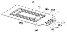
본 발명에 따른 안테나유닛(100)은 도 1 및 도 2에 도시된 바와 같이 회로기판(110), 패턴부(120) 및 리드부(130)를 포함한다.The
먼저, 상기 안테나유닛(100)은 휴대폰, PDA, PMP, 테블릿, 멀티미디어 기기 등과 같은 휴대용 전자기기와 무선 고주파 신호를 송출하거나 수신하여 소정의 기능을 수행토록 하기 위한 것이다.First, the
즉, 상기 안테나유닛(100)은 송출되거나 수신되는 무선 전력 신호를 통해 전자기 유도 현상에 기초한 유도 결합 방식을 이용하여 전력을 전달할 수 있도록 구비되어 수신안테나의 역할을 수행할 수도 있고 전송안테나의 역할을 수행할 수도 있다.That is, the
이러한 안테나유닛(100)은 회로기판(110)의 일면에 소정의 기능을 수행하기 위한 패턴부(120)가 적어도 하나 이상 구비된다.The
즉, 상기 패턴부(120)는 시계방향 또는 반시계 방향으로 권선되는 원형, 타원형, 나선형 또는 사각형상과 같은 다각형상의 형태로 구비될 수 있다. 이와 같은 패턴부(120)는 코일로 구성될 수도 있고 동박 등과 같은 금속박을 에칭하여 구성될 수도 있다.That is, the
여기서, 상기 회로기판(110)은 그 상면에 적어도 하나의 안테나패턴과 회로부가 형성되는 기재가 되는 요소로서, 내열성 및 내압성을 가지며, 가요성(flexible)을 갖는 소재이다. 이러한 소재의 물성을 고려할 때, 상기 회로기판(110)으로서 열경화성 고분자 필름인 PI나 PET 등과 같은 필름이 채용될 수 있다. 특히, 폴리이미드 필름은 통상 영상 400도 이상의 고온이나 영하 269도의 저온을 견디고, 초내열성과 초내한성을 지니고 있으며, 얇고 굴곡성이 뛰어날 뿐만 아니라 내화학성, 내마모성도 강해 열악한 환경에서 안정적인 성능을 유지할 수 있기 때문이다.Here, the
더불어, 상기 회로기판(110)의 일측에는 회로부(미도시) 또는 전자기기와의 전기적인 연결을 위한 연결단자(151a,151b,152a,152b,153a,153b)가 상기 패턴부의 개수와 대응되도록 구비된다.In addition, a
이때, 상기 패턴부(120)는 도 1 및 도 2에 도시된 바와 같이 서로 다른 기능을 수행하는 세 개의 패턴으로 구비될 수 있다. 여기서, 상기 세 개의 패턴은 무선 충전을 위한 WPT(Wireless Power Transfer) 패턴(121), 근거리 통신을 위한 MST(Magnetic secure transmission) 패턴(122) 및 NFC(Near Field Communication) 패턴(123)일 수 있다.In this case, the
여기서, 상기 WPT 패턴은 무선 충전에 사용되는 안테나 패턴이고, 상기 MST 패턴 및 NFC 패턴은 결제와 같은 근거리 통신에 사용되는 안테나 패턴이다.Here, the WPT pattern is an antenna pattern used for wireless charging, and the MST pattern and the NFC pattern are antenna patterns used in short distance communication such as settlement.
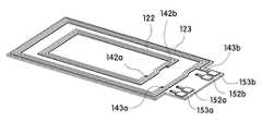
더불어, 상기 패턴부(120)는 상기 회로기판(110)의 일면에 소정의 기능을 수행하는 패턴이 각각 한 개씩 구비될 수도 있고, 도 4에 도시된 바와 같이 서로 다른 역할을 수행하는 2개의 패턴이 조합된 형태일 수 있다.In addition, the
즉, 상기 패턴부(120)는 WPT 패턴(121) 및 MST 패턴(122)의 두 가지 형태로 구비될 수도 있고(도 4a 참조), WPT 패턴(121) 및 NFC 패턴(123)의 두 가지 형태로 구비될 수도 있으며(도 4b 참조), MST 패턴(122) 및 NFC 패턴(123)의 두 가지 형태로 구비될 수도 있다(도 4c 참조).That is, the
여기서, 상기 NFC 패턴(123)과 WPT 패턴(121)이 동시에 구비되는 경우, 상기 NFC 패턴(123)은 WPT 패턴(121) 보다 주파수 대역이 높기 때문에 회로기판(110)의 외곽을 따라 미세한 선폭의 직사각형 형태로 도전성 패턴으로 형성되고, WPT 패턴(121)은 전력 전송이 요구되며 NFC 패턴(123)보다 낮은 주파수 대역을 사용하므로 NFC 패턴(123)의 내측에 NFC 패턴(123)의 선폭보다 넓은 선폭으로 형성될 수 있다.When the
이하에서는, 설명의 편의상 상기 패턴부가 상기 회로기판(110)의 일면에 배선 패턴의 형태로 구비되고, WPT 패턴(121), MST 패턴(122) 및 NFC 패턴(123)의 세 가지 패턴으로 구비되며, 회로기판(110)의 중앙부에서 테두리 측 방향으로 WPT 패턴(121), MST 패턴(122) 및 NFC 패턴(123)이 순차적으로 배열되는 것으로 설명하기로 한다.Hereinafter, for the sake of convenience, the pattern portion is provided on one surface of the
한편, 상기 복수 개의 패턴(121,122,123)의 양 단부에는 상기 회로기판(110)의 일측에 구비된 연결단자(151a,151b,152a,152b,153a,153b)와 전기적인 연결을 위한 접속단자(141a,141b,142a,142b,143a,143b)가 구비된다.At both ends of the plurality of
이때, 상기 접속단자 및 연결단자는 서로 직접 연결될 수도 있지만, 상기 회로기판(110) 상에서 상기 패턴(121,122,123)이 형성되는 면과 반대면에 배치되는 별도의 리드부(130)를 매개로 서로 전기적으로 연결될 수 있다.At this time, the connection terminals and the connection terminals may be directly connected to each other, but they may be electrically connected to each other via a
이는, 복수 개의 안테나 패턴이 구비되는 경우 최외곽측에 배치되는 NFC 패턴(123)의 내측 접속단자(143a)와, 내측에 배치되는 WPT 패턴(121)의 접속단자(141a,141b) 및 MST 패턴(122)의 접속단자(142a,142b)를 동일면 상에서 서로 대응되는 연결단자(151a,151b,152a,152b,153a)와 직접 연결하게 되면 접속단자(141a,141b,142a,142b,143a)와 연결단자(151a,151b,152a,152b,153a) 사이에 각각의 패턴들이 연결 경로 상에 존재하기 때문에 불가능하게 된다.This is because the
이에 따라, 상기 패턴이 형성된 회로기판(110)의 반대면 상에 상기 리드부(130)를 배치하여 접속단자(141a,141b,142a,142b,143a) 및 연결단자(151a,151b,152a,152b,153a)를 서로 전기적으로 연결하여 줌으로써 이러한 문제점을 해결할 수 있게 된다.Accordingly, the
구체적으로 설명하면, 최 내측에 배치되는 상기 WPT 패턴(121)의 내측 접속단자(141a)는 제1리드부(131)를 통해 제1연결단자(151a)와 연결되고, 상기 WPT 패턴(121)의 외측 접속단자(141b)는 제2리드부(132)를 통해 제2연결단자(151b)와 연결된다. 그리고, 상기 WPT 패턴(121) 및 NFC 패턴(123)의 사이에 존재하는 MST 패턴(122)의 내측 접속단자(142a)는 제3리드부(133)를 통해 제3연결단자(152a)와 연결되고, MST 패턴(122)의 외측 접속단자(142b)는 제4리드부(134)를 통해 제4연결단자(152b)와 연결된다. 더불어, 상기 NFC 패턴(123)의 내측 접속단자(143a)는 제5리드부(135)를 통해 제5연결단자(153a)와 연결되며, 상기 NFC 패턴(123)의 외측 접속단자(143b)는 제6연결단자(153b)와 직접 연결된다.More specifically, the
여기서, 상기 제1,2,3,4,5리드부(131,132,133,134,135)는 상기 패턴(121,122,123)들이 형성된 회로기판(110)의 일면과 반대면에 배치되며, 상기 최외곽측에 배치되는 NFC 패턴(123)의 외측 접속단자(143b)는 연결 경로상에 패턴이 존재하지 않으므로 동일평면상에 구비되는 연결단자(153b)와 직접 연결될 수 있게 된다.The first, second, third, fourth, and fifth
또한, 상기 리드부(130)는 상기 접속단자(141a,141b,142a,142b,143a) 및 연결단자(151a,151b,152a,152b,153a)를 전기적으로 연결하기 위한 전도성 브릿지로서, 전도성 페이스트를 통해 패턴인쇄될 수도 있고, 구리 등과 같은 전도성 금속이 도금된 형태일 수 있다.The
더불어, 상기 접속단자(141a,141b,142a,142b,143a) 및 연결단자(151a,151b,152a,152b,153a)는 상기 회로기판(110)을 관통하는 비아홀(161,162)을 통해 상기 리드부(130)의 양 단부측과 각각 전기적으로 연결된다.In addition, the
이때, 상기 접속단자(141a,141b,142a,142b,143a)와 연결단자(151a,151b,152a,152b,153a)를 전기적으로 연결하기 위한 브릿지 역할을 수행하는 리드부(130)의 두께(t2)는 상기 회로기판(110)의 반대면에 형성되는 패턴부(120)의 두께(t1)보다 더 얇은 두께를 갖도록 구비될 수 있다.The thickness t2 of the
즉, 상기 리드부(130)의 두께(t2)는 상기 패턴부(120)의 두께(t1)에 대하여 1/8 ~ 1/10의 두께를 갖도록 형성될 수 있으며, 바람직하게는 상기 리드부(130)의 두께(t2)는 상기 패턴부(120)의 두께(t1)에 대하여 1/9인 두께를 갖도록 형성될 수 있다.That is, the thickness t2 of the
일례로서, 상기 리드부(130)의 두께(t2)는 12㎛의 두께로 형성될 수 있고, 상기 패턴부(120)의 두께(t1)는 108㎛의 두께로 형성될 수 있다.As an example, the thickness t2 of the
이는, 종래의 안테나유닛과 동일한 두께로 본 발명의 안테나유닛(100)을 형성하는 경우, 단순 브릿지 역할을 수행하는 리드부(130)의 두께를 줄여 실질적인 기능을 수행하는 패턴부(120)의 두께를 두껍게 형성시킴으로써 동일 길이에 대하여 단면적을 넓혀줄 수 있게 된다. 이에 따라, 상기 패턴부(120)의 저항을 줄이고 발열량을 줄여줌으로써 전체적인 효율을 높여줄 수 있게 된다.This is because when the
더불어, 상기 패턴부(120)의 두께를 종래와 동일하게 형성하는 경우 상기 리드부(130)에서 줄어든 두께만큼 전체적인 두께가 감소하게 되므로, 본 발명에 따른 안테나유닛(100)이 적용된 전자기기의 전체두께를 줄일 수 있어 박형화를 이루는데 효과적이다.In addition, when the thickness of the
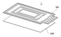
이와 같은 본 발명의 안테나유닛(100)은 무선전력 충전모듈(1)에 적용될 수 있다.The
즉, 도 5 및 도 7에 도시된 바와 같이, 본 발명의 일 실시예에 따른 무선전력 충전모듈(1)은 상기 안테나유닛(100)의 일면에 부착되는 차폐시트(200)를 포함한다.5 and 7, the wireless
상기 차폐시트(200)는 일정면적을 갖는 판상의 부재로 이루어지며, 상기 안테나유닛(100)에서 발생되는 자기장을 유기하는 역할을 수행한다.The
이러한 상기 차폐시트(200)은 단일 종류의 차폐시트가 단층으로 구성되거나 복수 개가 적층된 구조로 이루어질 수 있다.The
일례로, 상기 차폐시트(200)는 100~1000Wb/A·m 범위의 투자율을 갖도록 구비될 수 있다. 그러나 차폐시트(200)의 투자율을 이에 한정하는 것은 아니며 100Wb/A·m 이상의 투자율을 갖는 자성체를 사용하면 무방함을 밝혀둔다.For example, the shielding
이를 위해, 상기 차폐시트(200)는 비정질 합금의 리본시트 또는 나노결정립 합금의 리본시트가 사용될 수 있고, 폴리머 시트 또는 페라이트 시트가 사용될 수 있다.For this purpose, the shielding
여기서, 상기 비정질 합금 또는 나노결정립 합금은 Fe계 또는 Co계 자성 합금이 사용될 수 있다. 더불어, 상기 비정질 합금 및 나노결정립 합금은 3원소 합금 또는 5원소 합금을 포함할 수 있고, 예를 들어, 상기 3원소 합금은 Fe, Si 및 B를 포함하며, 상기 5원소 합금은 Fe, Si, B, Cu 및 Nb를 포함할 수 있다.Here, the amorphous alloy or the nanocrystalline alloy may be an Fe-based or a Co-based magnetic alloy. In addition, the amorphous alloy and the nanocrystalline alloy may include a three-element alloy or a five-element alloy. For example, the three-element alloy may include Fe, Si, and B, B, Cu and Nb.
그리고, 상기 페라이트 시트는 소결 페라이트 시트로 이루어질 수 있으며, MnZn 페라이트 또는 NiZn 페라이트로 이루어질 수 있다. 바람직하게는 상기 페라이트 시트가 NiZn 소결 페라이트로 이루어질 수 있다. 더불어, 상기 폴리머 시트는 비정질 합금 분말, 연자성체 분말, 센더스트와 같은 고투자율의 자성분말과 수지로 이루어질 수 있다.The ferrite sheet may be a sintered ferrite sheet, and may be composed of MnZn ferrite or NiZn ferrite. Preferably, the ferrite sheet may be made of NiZn sintered ferrite. In addition, the polymer sheet may be made of a magnetic powder and a high magnetic permeability resin such as an amorphous alloy powder, a soft magnetic body powder, and a sensor dust.
한편, 상기 차폐시트(200)는 도 6에 도시된 바와 같이 2층 이상의 복수 개의 비정질합금 또는 나노결정립 합금의 리본시트 층(210,220,230)으로 구성될 수도 있음을 밝혀둔다.6, the
더불어, 상기 차폐시트(200)를 위에 언급한 종류로 한정하는 것은 아니며 자성의 성질을 갖는 물질이면 모두 사용될 수 있음을 밝혀둔다.In addition, it should be noted that the
이때, 상기 차폐시트(200)는 와전류의 발생을 억제할 수 있도록 복수 개의 미세 조각으로 분리 형성될 수 있으며, 복수 개의 미세 조각들은 서로 이웃하는 미세 조각들 간에 전체적으로 절연되거나 부분적으로 절연되도록 구비될 수 있다.At this time, the shielding
이때, 상기 복수 개의 미세 조각은 1㎛ ~ 3mm의 크기로 구비될 수 있으며, 각각의 조각들은 비정형으로 랜덤하게 이루어질 수 있다.At this time, the plurality of fine pieces may be formed to have a size of 1 to 3 mm, and each piece may be irregularly randomized.
그리고, 상기 차폐시트(200)가 복수 개의 시트층이 미세조각으로 분리형성되어 적층되는 경우 각각의 시트층 사이에는 비전도성 재질로 이루어진 접착층이 배치되어 서로 적층되는 한 쌍의 시트층 사이에 스며들 수 있도록 함으로써 상기 접착층이 각각의 시트층을 구성하는 복수 개의 미세 조각을 절연하는 역할을 수행할 수도 있다.When the
여기서, 상기 접착층은 접착제로 구비될 수도 있으며 필름 형태의 기재의 일면 또는 양면에 접착제가 도포된 형태로 구비될 수도 있다.Here, the adhesive layer may be formed of an adhesive or may be provided on one side or both sides of a substrate in the form of a film with an adhesive applied thereto.
한편, 상기 차폐시트(200)는 상기 안테나유닛(100)에 서로 다른 역할을 수행하는 복수 개의 패턴(121,122,123)에 대응하여 해당 패턴의 특성을 높여줄 수 있도록 서로 다른 종류의 시트층이 복수 개로 구비될 수도 있음을 밝혀둔다.Meanwhile, the shielding
일례로, 상기 차폐시트(200)는 서로 다른 투자율을 갖는 제1시트층 및 제2시트층이 적층되는 형태로 구비될 수 있고, 상기 제1시트층은 상기 제2시트층보다 상대적으로 높은 투자율을 갖는 재질로 이루어질 수 있다.For example, the shielding
여기서, 상대적으로 높은 투자율을 갖는 제1시트층은 WPT 패턴(121)의 특성을 향상시키기 위한 것이며, 상대적으로 낮은 투자율을 갖는 제2시트층은 NFC 패턴(123)의 특성을 향상시키기 위한 것이다.Here, the first sheet layer having a relatively high permeability is for improving the characteristics of the
이를 위해, 상기 제1시트층은 비정질 합금의 리본시트 또는 나노결정립 합금의 리본시트가 사용될 수 있고, 상기 제2시트층은 폴리머 시트 또는 페라이트 시트가 사용될 수 있다.To this end, the first sheet layer may be a ribbon sheet of an amorphous alloy or a ribbon sheet of a nanocrystalline alloy, and the second sheet layer may be a polymer sheet or a ferrite sheet.
이와 같은 본 발명의 일 실시예에 따른 무선전력 충전모듈(1)은 도 7에 도시된 바와 같이 휴대 단말기(10)의 리어 케이스 또는 백커버(12)의 내측에 설치될 수 있으며, 휴대 단말기에 별도로 장착되는 케이스에 설치될 수도 있다.The wireless
일 실시예로서, 본 발명에 따른 안테나유닛(100)이 무선전력 충전모듈(1)에 적용되는 것으로 도시하고 설명하였지만, 이에 한정하는 것은 아니며, 본 발명에 따른 안테나유닛(100)은 회로기판에 안테나 패턴을 갖는 안테나유닛이 적용되는 다양한 전자기기에 모두 사용될 수 있음을 밝혀둔다. 일례로, 상기 안테나유닛(100)은 셀룰러 폰, PCS 폰, GSM 폰, CDMA 폰과 같은 통상적인 이동 전화기, PMP, PDA, 스마트폰, MBS 폰 일 수 있으며, 디지타이저에도 적용될 수 있다.
Although the
이상에서 본 발명의 일 실시예에 대하여 설명하였으나, 본 발명의 사상은 본 명세서에 제시되는 실시 예에 제한되지 아니하며, 본 발명의 사상을 이해하는 당업자는 동일한 사상의 범위 내에서, 구성요소의 부가, 변경, 삭제, 추가 등에 의해서 다른 실시 예를 용이하게 제안할 수 있을 것이나, 이 또한 본 발명의 사상범위 내에 든다고 할 것이다.While the present invention has been particularly shown and described with reference to exemplary embodiments thereof, it is to be understood that the invention is not limited to the disclosed exemplary embodiments, It will be understood by those skilled in the art that various changes in form and details may be made therein without departing from the spirit and scope of the invention as defined by the appended claims.
1: 무선전력 충전모듈10 : 휴대 단말기
100 : 안테나유닛110 : 회로기판
120 : 패턴부121 : WPT 패턴
122 : MST 패턴123 : NFC 패턴
130 : 리드부131 : 제1리드부
132 : 제2리드부133 : 제3리드부
134 : 제4리드부135 : 제5리드부
141a,141b,142a,142b,143a,143b : 접속단자
151a,151b,152a,152b,153a,154b : 연결단자
161,162 : 비아홀200 : 차폐시트
210,220,230 : 비정질 합금 또는 나노 결정립 합금의 리본시트
240 : 접착층1: wireless power charging module 10: portable terminal
100: antenna unit 110: circuit board
120: pattern part 121: WPT pattern
122: MST pattern 123: NFC pattern
130: lead portion 131: first lead portion
132: second lead portion 133: third lead portion
134: fourth lead portion 135: fifth lead portion
141a, 141b, 142a, 142b, 143a, 143b:
151a, 151b, 152a, 152b, 153a, 154b:
161, 162: via hole 200: shielding sheet
210, 220, 230: ribbon sheet of amorphous alloy or nano-crystal alloy
240: adhesive layer
Claims (13)
Translated fromKorean양 단부측에 각각 접속단자가 구비되고, 상기 회로기판의 일면에 고유의 기능을 수행하도록 패턴형성되는 적어도 하나의 패턴부; 및
상기 각각의 접속단자를 연결단자와 전기적으로 연결하는 복수 개의 리드부;를 포함하고,
상기 복수 개의 리드부 중 상기 패턴부와 반대면에 구비되는 리드부는 상기 패턴부의 두께보다 더 얇은 두께를 갖도록 구비되는 안테나유닛.A circuit board;
At least one pattern portion provided with connection terminals on both ends and patterned to perform a function inherent to one surface of the circuit board; And
And a plurality of lead portions electrically connecting the connection terminals to the connection terminals,
Wherein a lead portion provided on a surface opposite to the pattern portion among the plurality of lead portions is formed to have a thickness thinner than the thickness of the pattern portion.
상기 패턴부는 WPT 패턴, MST 패턴 및 NFC 패턴 중 하나 이상의 패턴을 포함하는 안테나유닛.The method according to claim 1,
Wherein the pattern portion includes at least one of a WPT pattern, an MST pattern, and an NFC pattern.
상기 회로기판의 타면에 구비되는 리드부는 상기 회로기판을 관통하는 비아홀을 통해 상기 접속단자 및 연결단자와 각각 전기적으로 연결되는 안테나유닛.The method according to claim 1,
Wherein a lead portion provided on the other surface of the circuit board is electrically connected to the connection terminal and the connection terminal through a via hole passing through the circuit board.
상기 리드부는 상기 패턴부의 두께에 대하여 1/8~1/10의 두께를 갖도록 형성되는 안테나유닛.The method according to claim 1,
Wherein the lead portion is formed to have a thickness of 1/8 to 1/10 of the thickness of the pattern portion.
상기 리드부는 상기 패턴부의 두께에 대하여 1/9인 두께를 갖도록 형성되는 안테나유닛.5. The method of claim 4,
Wherein the lead portion is formed to have a thickness of 1/9 of the thickness of the pattern portion.
상기 안테나유닛의 일면에 배치되어 자기장을 유기하는 차폐시트;을 포함하는 무선전력 충전모듈.An antenna unit according to any one of claims 1 to 5; And
And a shielding sheet disposed on one surface of the antenna unit to induce a magnetic field.
상기 차폐시트는 비정질 합금의 리본시트 또는 나노 결정립 합금의 리본시트, 페라이트 시트 또는 폴리머 시트인 무선전력 충전모듈.The method according to claim 6,
Wherein the shielding sheet is a ribbon sheet of an amorphous alloy or a ribbon sheet of a nanocrystalline alloy, a ferrite sheet or a polymer sheet.
상기 차폐시트는 비정질 합금의 리본시트 또는 나노 결정립 합금의 리본시트가 복수층으로 적층되는 무선전력 충전모듈.The method according to claim 6,
Wherein the shielding sheet is formed by laminating a ribbon sheet of an amorphous alloy or a ribbon sheet of a nano-crystal alloy into a plurality of layers.
상기 페라이트 시트는 MnZn 페라이트 또는 NiZn 페라이트로 이루어진 무선전력 충전모듈.8. The method of claim 7,
Wherein the ferrite sheet is made of MnZn ferrite or NiZn ferrite.
상기 차폐시트는 복수 개의 미세 조각으로 분리형성되는 무선전력 충전모듈.The method according to claim 6,
Wherein the shielding sheet is divided into a plurality of minute pieces.
상기 복수 개의 미세 조각들은 서로 이웃하는 미세 조각들 간에 전체적으로 절연되거나 부분적으로 절연되는 무선전력 충전모듈.11. The method of claim 10,
Wherein the plurality of microparts are totally insulated or partially insulated between neighboring microparts.
상기 복수 개의 미세 조각은 1㎛ ~ 3mm의 크기인 무선전력 충전모듈.11. The method of claim 10,
Wherein the plurality of microparts have a size of 1 [mu] m to 3 mm.
상기 복수 개의 미세 조각은 비정형으로 이루어지는 무선전력 충전모듈.11. The method of claim 10,
Wherein the plurality of micro-pieces are atypical.
Priority Applications (1)
| Application Number | Priority Date | Filing Date | Title |
|---|---|---|---|
| KR1020150051088AKR102290168B1 (en) | 2015-04-10 | 2015-04-10 | multi antenna unit and wireless charging module having the same |
Applications Claiming Priority (1)
| Application Number | Priority Date | Filing Date | Title |
|---|---|---|---|
| KR1020150051088AKR102290168B1 (en) | 2015-04-10 | 2015-04-10 | multi antenna unit and wireless charging module having the same |
Publications (2)
| Publication Number | Publication Date |
|---|---|
| KR20160121279Atrue KR20160121279A (en) | 2016-10-19 |
| KR102290168B1 KR102290168B1 (en) | 2021-08-17 |
Family
ID=57250478
Family Applications (1)
| Application Number | Title | Priority Date | Filing Date |
|---|---|---|---|
| KR1020150051088AActiveKR102290168B1 (en) | 2015-04-10 | 2015-04-10 | multi antenna unit and wireless charging module having the same |
Country Status (1)
| Country | Link |
|---|---|
| KR (1) | KR102290168B1 (en) |
Cited By (3)
| Publication number | Priority date | Publication date | Assignee | Title |
|---|---|---|---|---|
| US20160308587A1 (en)* | 2015-04-14 | 2016-10-20 | Sang-Hyo Lee | Near field communication package and portable device including the same |
| US20170344999A1 (en)* | 2016-05-30 | 2017-11-30 | Samsung Electronics Co., Ltd. | Payment method and electronic device using loop antennas |
| KR20210157775A (en)* | 2020-06-22 | 2021-12-29 | 주식회사 아모센스 | antenna module |
Citations (3)
| Publication number | Priority date | Publication date | Assignee | Title |
|---|---|---|---|---|
| KR20140109336A (en)* | 2013-03-05 | 2014-09-15 | 주식회사 아모센스 | Composite Sheet for Shielding Magnetic Field and Electromagnetic Wave and Antenna Module Using the Same |
| KR101470131B1 (en)* | 2013-03-15 | 2014-12-05 | 엘지이노텍 주식회사 | Antenna assembly and manufacturing method thereof |
| KR20150011604A (en)* | 2013-07-23 | 2015-02-02 | 삼성전기주식회사 | Wireless charging device |
- 2015
- 2015-04-10KRKR1020150051088Apatent/KR102290168B1/enactiveActive
Patent Citations (3)
| Publication number | Priority date | Publication date | Assignee | Title |
|---|---|---|---|---|
| KR20140109336A (en)* | 2013-03-05 | 2014-09-15 | 주식회사 아모센스 | Composite Sheet for Shielding Magnetic Field and Electromagnetic Wave and Antenna Module Using the Same |
| KR101470131B1 (en)* | 2013-03-15 | 2014-12-05 | 엘지이노텍 주식회사 | Antenna assembly and manufacturing method thereof |
| KR20150011604A (en)* | 2013-07-23 | 2015-02-02 | 삼성전기주식회사 | Wireless charging device |
Cited By (7)
| Publication number | Priority date | Publication date | Assignee | Title |
|---|---|---|---|---|
| US20160308587A1 (en)* | 2015-04-14 | 2016-10-20 | Sang-Hyo Lee | Near field communication package and portable device including the same |
| US10651897B2 (en)* | 2015-04-14 | 2020-05-12 | Samsung Electronics Co., Ltd | Near field communication package and portable device including the same |
| US20170344999A1 (en)* | 2016-05-30 | 2017-11-30 | Samsung Electronics Co., Ltd. | Payment method and electronic device using loop antennas |
| KR20210157775A (en)* | 2020-06-22 | 2021-12-29 | 주식회사 아모센스 | antenna module |
| WO2021261833A1 (en)* | 2020-06-22 | 2021-12-30 | 주식회사 아모센스 | Antenna module |
| US20230238702A1 (en)* | 2020-06-22 | 2023-07-27 | AMOSENSE Co.,Ltd | Antenna module |
| US12206186B2 (en) | 2020-06-22 | 2025-01-21 | Amosense Co., Ltd | Antenna module |
Also Published As
| Publication number | Publication date |
|---|---|
| KR102290168B1 (en) | 2021-08-17 |
Similar Documents
| Publication | Publication Date | Title |
|---|---|---|
| US10658740B2 (en) | Antenna unit and wireless power transmission module including same | |
| CN108184333B (en) | Combined antenna module | |
| US11087912B2 (en) | Magnetic field shield sheet for wireless power transmission and wireless power receiving module comprising same | |
| US10658870B2 (en) | Combo antenna unit and wireless power receiving module comprising same | |
| US9905926B2 (en) | Antenna device and wireless communication apparatus | |
| CN103765675B (en) | Antenna device and communication terminal device | |
| CN106415929B (en) | Multi-antenna and wireless device provided with same | |
| KR102056262B1 (en) | Antenna unit for a wireless charging and wireless charging module having the same | |
| CN107646157B (en) | Shielding unit for wireless charging and wireless power transmission module comprising shielding unit | |
| US11282639B2 (en) | Antenna device and electronic apparatus | |
| US20190252768A1 (en) | Antenna module and electronic device having the same | |
| US20190341692A1 (en) | Antenna device and electronic appliance | |
| CN207926288U (en) | Magnetic field shielding structure and the mobile device for including the magnetic field shielding structure | |
| US20190386389A1 (en) | Antenna device, communication system, and electronic apparatus | |
| KR20160100786A (en) | Shielding unit for combo antenna and wireless charging module having the same | |
| KR20180132205A (en) | wireless power transfer module | |
| KR20160121279A (en) | multi antenna unit and wireless charging module having the same | |
| US10855108B2 (en) | Wireless device | |
| US10903557B2 (en) | Antenna device and electronic device | |
| US10840738B2 (en) | Wireless device | |
| JP2013247554A (en) | Antenna device and communication terminal device | |
| JP2020108102A (en) | Antenna device and electronic equipment | |
| JP6558520B1 (en) | ANTENNA DEVICE AND ELECTRONIC DEVICE | |
| KR102339683B1 (en) | Heat radiation unit for a wireless charging and wireless charging module having the same | |
| CN106684547A (en) | NFC (near field communication) antenna with low-frequency interference for high-frequency antennas |
Legal Events
| Date | Code | Title | Description |
|---|---|---|---|
| PA0109 | Patent application | St.27 status event code:A-0-1-A10-A12-nap-PA0109 | |
| R17-X000 | Change to representative recorded | St.27 status event code:A-3-3-R10-R17-oth-X000 | |
| PG1501 | Laying open of application | St.27 status event code:A-1-1-Q10-Q12-nap-PG1501 | |
| P11-X000 | Amendment of application requested | St.27 status event code:A-2-2-P10-P11-nap-X000 | |
| P13-X000 | Application amended | St.27 status event code:A-2-2-P10-P13-nap-X000 | |
| R15-X000 | Change to inventor requested | St.27 status event code:A-3-3-R10-R15-oth-X000 | |
| R16-X000 | Change to inventor recorded | St.27 status event code:A-3-3-R10-R16-oth-X000 | |
| P22-X000 | Classification modified | St.27 status event code:A-2-2-P10-P22-nap-X000 | |
| P22-X000 | Classification modified | St.27 status event code:A-2-2-P10-P22-nap-X000 | |
| P11-X000 | Amendment of application requested | St.27 status event code:A-2-2-P10-P11-nap-X000 | |
| P13-X000 | Application amended | St.27 status event code:A-2-2-P10-P13-nap-X000 | |
| PA0201 | Request for examination | St.27 status event code:A-1-2-D10-D11-exm-PA0201 | |
| D13-X000 | Search requested | St.27 status event code:A-1-2-D10-D13-srh-X000 | |
| PN2301 | Change of applicant | St.27 status event code:A-3-3-R10-R13-asn-PN2301 St.27 status event code:A-3-3-R10-R11-asn-PN2301 | |
| D14-X000 | Search report completed | St.27 status event code:A-1-2-D10-D14-srh-X000 | |
| E902 | Notification of reason for refusal | ||
| PE0902 | Notice of grounds for rejection | St.27 status event code:A-1-2-D10-D21-exm-PE0902 | |
| E13-X000 | Pre-grant limitation requested | St.27 status event code:A-2-3-E10-E13-lim-X000 | |
| P11-X000 | Amendment of application requested | St.27 status event code:A-2-2-P10-P11-nap-X000 | |
| P13-X000 | Application amended | St.27 status event code:A-2-2-P10-P13-nap-X000 | |
| E701 | Decision to grant or registration of patent right | ||
| PE0701 | Decision of registration | St.27 status event code:A-1-2-D10-D22-exm-PE0701 | |
| GRNT | Written decision to grant | ||
| PR0701 | Registration of establishment | St.27 status event code:A-2-4-F10-F11-exm-PR0701 | |
| PR1002 | Payment of registration fee | St.27 status event code:A-2-2-U10-U11-oth-PR1002 Fee payment year number:1 | |
| PG1601 | Publication of registration | St.27 status event code:A-4-4-Q10-Q13-nap-PG1601 | |
| PN2301 | Change of applicant | St.27 status event code:A-5-5-R10-R13-asn-PN2301 St.27 status event code:A-5-5-R10-R11-asn-PN2301 | |
| PR1001 | Payment of annual fee | St.27 status event code:A-4-4-U10-U11-oth-PR1001 Fee payment year number:4 | |
| PR1001 | Payment of annual fee | St.27 status event code:A-4-4-U10-U11-oth-PR1001 Fee payment year number:5 |