KR20160121059A - Method of forming fine patterns - Google Patents
Method of forming fine patternsDownload PDFInfo
- Publication number
- KR20160121059A KR20160121059AKR1020150050478AKR20150050478AKR20160121059AKR 20160121059 AKR20160121059 AKR 20160121059AKR 1020150050478 AKR1020150050478 AKR 1020150050478AKR 20150050478 AKR20150050478 AKR 20150050478AKR 20160121059 AKR20160121059 AKR 20160121059A
- Authority
- KR
- South Korea
- Prior art keywords
- resist
- regions
- acids
- patterns
- region
- Prior art date
- Legal status (The legal status is an assumption and is not a legal conclusion. Google has not performed a legal analysis and makes no representation as to the accuracy of the status listed.)
- Withdrawn
Links
- 238000000034methodMethods0.000titleclaimsdescription87
- 239000002253acidSubstances0.000claimsabstractdescription100
- 238000009792diffusion processMethods0.000claimsabstractdescription66
- 150000007513acidsChemical class0.000claimsabstractdescription54
- 238000000059patterningMethods0.000claimsabstractdescription12
- 238000000137annealingMethods0.000claimsdescription33
- 239000003960organic solventSubstances0.000claimsdescription31
- 229920000642polymerPolymers0.000claimsdescription24
- 125000006239protecting groupChemical group0.000claimsdescription18
- 239000003513alkaliSubstances0.000claimsdescription13
- 230000002378acidificating effectEffects0.000claimsdescription9
- RTZKZFJDLAIYFH-UHFFFAOYSA-NDiethyl etherChemical compoundCCOCCRTZKZFJDLAIYFH-UHFFFAOYSA-N0.000claimsdescription8
- 230000001737promoting effectEffects0.000claimsdescription8
- WGTYBPLFGIVFAS-UHFFFAOYSA-Mtetramethylammonium hydroxideChemical compound[OH-].C[N+](C)(C)CWGTYBPLFGIVFAS-UHFFFAOYSA-M0.000claimsdescription8
- QTBSBXVTEAMEQO-UHFFFAOYSA-MAcetateChemical compoundCC([O-])=OQTBSBXVTEAMEQO-UHFFFAOYSA-M0.000claimsdescription4
- LFQSCWFLJHTTHZ-UHFFFAOYSA-NEthanolChemical compoundCCOLFQSCWFLJHTTHZ-UHFFFAOYSA-N0.000claimsdescription4
- 150000002148estersChemical class0.000claimsdescription4
- 150000002576ketonesChemical class0.000claimsdescription4
- 239000012298atmosphereSubstances0.000claimsdescription3
- 239000007864aqueous solutionSubstances0.000claimsdescription2
- IXCSERBJSXMMFS-UHFFFAOYSA-Nhcl hclChemical compoundCl.ClIXCSERBJSXMMFS-UHFFFAOYSA-N0.000claims1
- 238000006243chemical reactionMethods0.000description11
- 239000000463materialSubstances0.000description9
- 239000000758substrateSubstances0.000description9
- 239000004065semiconductorSubstances0.000description7
- 239000000243solutionSubstances0.000description7
- 238000010511deprotection reactionMethods0.000description5
- FFUAGWLWBBFQJT-UHFFFAOYSA-NhexamethyldisilazaneChemical compoundC[Si](C)(C)N[Si](C)(C)CFFUAGWLWBBFQJT-UHFFFAOYSA-N0.000description5
- 238000004519manufacturing processMethods0.000description5
- 239000002086nanomaterialSubstances0.000description5
- 239000003795chemical substances by applicationSubstances0.000description3
- 230000009477glass transitionEffects0.000description3
- 125000002887hydroxy groupChemical group[H]O*0.000description3
- 238000000206photolithographyMethods0.000description3
- 239000000047productSubstances0.000description3
- 239000002683reaction inhibitorSubstances0.000description3
- 239000012670alkaline solutionSubstances0.000description2
- 230000015572biosynthetic processEffects0.000description2
- 239000011248coating agentSubstances0.000description2
- 238000000576coating methodMethods0.000description2
- 238000009826distributionMethods0.000description2
- 125000006850spacer groupChemical group0.000description2
- -1t-butyloxycarbonylChemical group0.000description2
- CERQOIWHTDAKMF-UHFFFAOYSA-MMethacrylateChemical compoundCC(=C)C([O-])=OCERQOIWHTDAKMF-UHFFFAOYSA-M0.000description1
- BLRPTPMANUNPDV-UHFFFAOYSA-NSilaneChemical compound[SiH4]BLRPTPMANUNPDV-UHFFFAOYSA-N0.000description1
- 229920006109alicyclic polymerPolymers0.000description1
- 239000006117anti-reflective coatingSubstances0.000description1
- 230000003667anti-reflective effectEffects0.000description1
- 239000002585baseSubstances0.000description1
- 210000000988bone and boneAnatomy0.000description1
- 239000003054catalystSubstances0.000description1
- 238000006555catalytic reactionMethods0.000description1
- 239000007795chemical reaction productSubstances0.000description1
- 238000004140cleaningMethods0.000description1
- 238000011109contaminationMethods0.000description1
- 230000007547defectEffects0.000description1
- 230000008021depositionEffects0.000description1
- 238000005530etchingMethods0.000description1
- 239000012467final productSubstances0.000description1
- 239000000446fuelSubstances0.000description1
- 230000014509gene expressionEffects0.000description1
- 230000002209hydrophobic effectEffects0.000description1
- 230000001939inductive effectEffects0.000description1
- 239000003112inhibitorSubstances0.000description1
- 239000013067intermediate productSubstances0.000description1
- 230000001788irregularEffects0.000description1
- 239000004973liquid crystal related substanceSubstances0.000description1
- 238000001459lithographyMethods0.000description1
- FPYJFEHAWHCUMM-UHFFFAOYSA-Nmaleic anhydrideChemical compoundO=C1OC(=O)C=C1FPYJFEHAWHCUMM-UHFFFAOYSA-N0.000description1
- 239000011159matrix materialSubstances0.000description1
- 238000012986modificationMethods0.000description1
- 230000004048modificationEffects0.000description1
- 239000002070nanowireSubstances0.000description1
- JRZJOMJEPLMPRA-UHFFFAOYSA-NolefinNatural productsCCCCCCCC=CJRZJOMJEPLMPRA-UHFFFAOYSA-N0.000description1
- 230000003287optical effectEffects0.000description1
- 230000010363phase shiftEffects0.000description1
- 229920002120photoresistant polymerPolymers0.000description1
- 238000006862quantum yield reactionMethods0.000description1
- 229910000077silaneInorganic materials0.000description1
- 239000010409thin filmSubstances0.000description1
- 229920003169water-soluble polymerPolymers0.000description1
Images


Classifications
- G—PHYSICS
- G03—PHOTOGRAPHY; CINEMATOGRAPHY; ANALOGOUS TECHNIQUES USING WAVES OTHER THAN OPTICAL WAVES; ELECTROGRAPHY; HOLOGRAPHY
- G03F—PHOTOMECHANICAL PRODUCTION OF TEXTURED OR PATTERNED SURFACES, e.g. FOR PRINTING, FOR PROCESSING OF SEMICONDUCTOR DEVICES; MATERIALS THEREFOR; ORIGINALS THEREFOR; APPARATUS SPECIALLY ADAPTED THEREFOR
- G03F7/00—Photomechanical, e.g. photolithographic, production of textured or patterned surfaces, e.g. printing surfaces; Materials therefor, e.g. comprising photoresists; Apparatus specially adapted therefor
- G03F7/26—Processing photosensitive materials; Apparatus therefor
- G03F7/30—Imagewise removal using liquid means
- G03F7/32—Liquid compositions therefor, e.g. developers
- G03F7/325—Non-aqueous compositions
- G—PHYSICS
- G03—PHOTOGRAPHY; CINEMATOGRAPHY; ANALOGOUS TECHNIQUES USING WAVES OTHER THAN OPTICAL WAVES; ELECTROGRAPHY; HOLOGRAPHY
- G03F—PHOTOMECHANICAL PRODUCTION OF TEXTURED OR PATTERNED SURFACES, e.g. FOR PRINTING, FOR PROCESSING OF SEMICONDUCTOR DEVICES; MATERIALS THEREFOR; ORIGINALS THEREFOR; APPARATUS SPECIALLY ADAPTED THEREFOR
- G03F7/00—Photomechanical, e.g. photolithographic, production of textured or patterned surfaces, e.g. printing surfaces; Materials therefor, e.g. comprising photoresists; Apparatus specially adapted therefor
- G03F7/004—Photosensitive materials
- G03F7/039—Macromolecular compounds which are photodegradable, e.g. positive electron resists
- G03F7/0392—Macromolecular compounds which are photodegradable, e.g. positive electron resists the macromolecular compound being present in a chemically amplified positive photoresist composition
- G—PHYSICS
- G03—PHOTOGRAPHY; CINEMATOGRAPHY; ANALOGOUS TECHNIQUES USING WAVES OTHER THAN OPTICAL WAVES; ELECTROGRAPHY; HOLOGRAPHY
- G03F—PHOTOMECHANICAL PRODUCTION OF TEXTURED OR PATTERNED SURFACES, e.g. FOR PRINTING, FOR PROCESSING OF SEMICONDUCTOR DEVICES; MATERIALS THEREFOR; ORIGINALS THEREFOR; APPARATUS SPECIALLY ADAPTED THEREFOR
- G03F7/00—Photomechanical, e.g. photolithographic, production of textured or patterned surfaces, e.g. printing surfaces; Materials therefor, e.g. comprising photoresists; Apparatus specially adapted therefor
- G03F7/20—Exposure; Apparatus therefor
- G—PHYSICS
- G03—PHOTOGRAPHY; CINEMATOGRAPHY; ANALOGOUS TECHNIQUES USING WAVES OTHER THAN OPTICAL WAVES; ELECTROGRAPHY; HOLOGRAPHY
- G03F—PHOTOMECHANICAL PRODUCTION OF TEXTURED OR PATTERNED SURFACES, e.g. FOR PRINTING, FOR PROCESSING OF SEMICONDUCTOR DEVICES; MATERIALS THEREFOR; ORIGINALS THEREFOR; APPARATUS SPECIALLY ADAPTED THEREFOR
- G03F7/00—Photomechanical, e.g. photolithographic, production of textured or patterned surfaces, e.g. printing surfaces; Materials therefor, e.g. comprising photoresists; Apparatus specially adapted therefor
- G03F7/26—Processing photosensitive materials; Apparatus therefor
- G03F7/30—Imagewise removal using liquid means
- G03F7/32—Liquid compositions therefor, e.g. developers
- G03F7/322—Aqueous alkaline compositions
- G—PHYSICS
- G03—PHOTOGRAPHY; CINEMATOGRAPHY; ANALOGOUS TECHNIQUES USING WAVES OTHER THAN OPTICAL WAVES; ELECTROGRAPHY; HOLOGRAPHY
- G03F—PHOTOMECHANICAL PRODUCTION OF TEXTURED OR PATTERNED SURFACES, e.g. FOR PRINTING, FOR PROCESSING OF SEMICONDUCTOR DEVICES; MATERIALS THEREFOR; ORIGINALS THEREFOR; APPARATUS SPECIALLY ADAPTED THEREFOR
- G03F7/00—Photomechanical, e.g. photolithographic, production of textured or patterned surfaces, e.g. printing surfaces; Materials therefor, e.g. comprising photoresists; Apparatus specially adapted therefor
- G03F7/26—Processing photosensitive materials; Apparatus therefor
- G03F7/40—Treatment after imagewise removal, e.g. baking
- G03F7/405—Treatment with inorganic or organometallic reagents after imagewise removal
- G—PHYSICS
- G03—PHOTOGRAPHY; CINEMATOGRAPHY; ANALOGOUS TECHNIQUES USING WAVES OTHER THAN OPTICAL WAVES; ELECTROGRAPHY; HOLOGRAPHY
- G03F—PHOTOMECHANICAL PRODUCTION OF TEXTURED OR PATTERNED SURFACES, e.g. FOR PRINTING, FOR PROCESSING OF SEMICONDUCTOR DEVICES; MATERIALS THEREFOR; ORIGINALS THEREFOR; APPARATUS SPECIALLY ADAPTED THEREFOR
- G03F9/00—Registration or positioning of originals, masks, frames, photographic sheets or textured or patterned surfaces, e.g. automatically
- G03F9/70—Registration or positioning of originals, masks, frames, photographic sheets or textured or patterned surfaces, e.g. automatically for microlithography
- H—ELECTRICITY
- H01—ELECTRIC ELEMENTS
- H01L—SEMICONDUCTOR DEVICES NOT COVERED BY CLASS H10
- H01L21/00—Processes or apparatus adapted for the manufacture or treatment of semiconductor or solid state devices or of parts thereof
- H01L21/02—Manufacture or treatment of semiconductor devices or of parts thereof
- H01L21/027—Making masks on semiconductor bodies for further photolithographic processing not provided for in group H01L21/18 or H01L21/34
- H01L21/0271—Making masks on semiconductor bodies for further photolithographic processing not provided for in group H01L21/18 or H01L21/34 comprising organic layers
- H01L21/0273—Making masks on semiconductor bodies for further photolithographic processing not provided for in group H01L21/18 or H01L21/34 comprising organic layers characterised by the treatment of photoresist layers
- H—ELECTRICITY
- H01—ELECTRIC ELEMENTS
- H01L—SEMICONDUCTOR DEVICES NOT COVERED BY CLASS H10
- H01L21/00—Processes or apparatus adapted for the manufacture or treatment of semiconductor or solid state devices or of parts thereof
- H01L21/70—Manufacture or treatment of devices consisting of a plurality of solid state components formed in or on a common substrate or of parts thereof; Manufacture of integrated circuit devices or of parts thereof
- H01L21/71—Manufacture of specific parts of devices defined in group H01L21/70
- H01L21/768—Applying interconnections to be used for carrying current between separate components within a device comprising conductors and dielectrics
- H01L21/76801—Applying interconnections to be used for carrying current between separate components within a device comprising conductors and dielectrics characterised by the formation and the after-treatment of the dielectrics, e.g. smoothing
- H01L21/76802—Applying interconnections to be used for carrying current between separate components within a device comprising conductors and dielectrics characterised by the formation and the after-treatment of the dielectrics, e.g. smoothing by forming openings in dielectrics
- H01L21/76816—Aspects relating to the layout of the pattern or to the size of vias or trenches
Landscapes
- Physics & Mathematics (AREA)
- General Physics & Mathematics (AREA)
- Engineering & Computer Science (AREA)
- Computer Hardware Design (AREA)
- Condensed Matter Physics & Semiconductors (AREA)
- Manufacturing & Machinery (AREA)
- Spectroscopy & Molecular Physics (AREA)
- Microelectronics & Electronic Packaging (AREA)
- Power Engineering (AREA)
- Chemical & Material Sciences (AREA)
- Inorganic Chemistry (AREA)
- Organic Chemistry (AREA)
- Photosensitive Polymer And Photoresist Processing (AREA)
Abstract
Translated fromKorean
Description
Translated fromKorean본 출원은 반도체 기술에 관한 것으로서, 보다 상세하게는 미세 패턴 형성 방법에 관한 것이다.The present application relates to semiconductor technology, and more particularly, to a method for forming a fine pattern.
반도체 산업이 급속히 성장되며, 보다 높은 소자 밀도를 갖는 집적 회로를 구현하고자 노력하고 있다. 평면적으로 단위 셀(cell)이 차지는 면적을 감소시켜, 보다 많은 수의 소자들을 제한된 면적 내에 집적시키기 위해서, 수 내지 수십 ㎚의 수준의 나노 스케일(nano scale)의 선폭(CD: Critical Dimension)을 가지는 패턴 구조를 구현하기 위해 다양한 기술들이 시도되고 있다.The semiconductor industry is rapidly growing, and efforts are being made to realize integrated circuits with higher device densities. In order to reduce the area occupied by a unit cell in a planar manner and to integrate a larger number of devices into a limited area, a nano scale critical dimension (CD) of several nanometers to several tens of nanometers A variety of techniques have been attempted to implement the pattern structure.
반도체 소자의 나노 스케일의 미세 패턴을 단순 포토리소그래피(photo lithography) 기술에 의존하여 형성할 때, 리소그래피 장비의 이미지(image) 분해능에 대한 한계로 보다 미세한 크기의 패턴을 구현하는 데 제약이 있다. 포토리소그래피 기술에 사용되는 광원의 파장 및 광학 시스템(system)의 해상 한계로 인한 분해능 제약을 극복하여 미세 패턴들의 배열을 형성하기 위한 방법의 개발이 요구되고 있다.When forming nanoscale fine patterns of semiconductor devices in dependence on simple photo lithography techniques, there is a limitation in implementing finer size patterns due to limitations on the image resolution of lithography equipment. There is a need to develop a method for forming an array of fine patterns that overcomes the resolution limitation due to the wavelength of the light source used in the photolithography technique and the resolution limit of the optical system.
더블 패터닝 기술(double patterning technology)이나 스페이서 패터닝 기술(spacer patterning technology)들이 리소그래피 장비의 분해능을 극복하고자 제시되고 있으나, 다수의 층들의 증착, 노광, 식각, 및 세정 과정들이 요구되고 있어 상당히 복잡한 공정 단계들을 수반하고 있다. 리소그래피 장비의 분해능을 극복하여 보다 미세한 패턴들을 형성하고자 많은 노력들이 시도되고 있다.Double patterning technology or spacer patterning techniques are proposed to overcome the resolution of lithographic equipment, but deposition, exposure, etching, and cleaning processes of multiple layers are required, . Numerous efforts have been made to overcome the resolution of lithographic equipment to form finer patterns.
본 출원은 노광 과정에서의 해상도 한계를 극복하여 미세한 크기의 선폭을 가지는 미세 패턴들을 형성하는 방법을 제시하고자 한다.This application proposes a method of forming fine patterns having a fine line width overcoming the resolution limit in the exposure process.
본 출원의 일 관점은, 화학증폭형 레지스트층(layer of chemically amplified resist)의 제1영역들에 산(acid)들을 발생시키는 노광 단계; 상기 노광된 제1영역들을 제1현상하여 제1오프닝 홀(hole) 형상들을 제공하는 레지스트 제1패턴들을 형성하는 단계; 상기 레지스트 제1패턴들의 측벽 부분들에 잔존하는 상기 산들을 내측으로 확산(diffusion)하고 상기 산들이 확산된 제2영역들이 상호 맞닿도록 연장하여 중앙 부분에 상기 산들이 확산되지 못한 제3영역들을 고립된 섬(isolated island) 형상으로 형성하는 단계; 및 상기 제3영역들을 제2현상하여 상기 제1오프닝 홀 형상들로 둘러싸인 제2오프닝 홀 형상들을 제공하는 레지스트 제2패턴들을 패터닝하는 단계를 포함하는 미세 패턴 형성 방법을 제시한다.One aspect of the present application includes an exposure step of generating acids in first regions of a chemically amplified resist layer; Forming first resist patterns that provide first opening hole shapes by first developing the exposed first areas; Diffusion of the acids remaining in the sidewall portions of the first patterns of resist is extended inward so that the second regions of the acid diffused are mutually abutted and the third regions in which the acids are not diffused in the central portion are isolated Forming an island in an island shape; And patterning the second resist patterns to form second opening hole shapes surrounded by the first opening hole shapes by performing a second development of the third regions.
본 출원의 일 관점은, 화학증폭형 레지스트층(layer of chemically amplified resist)의 제1영역들에 산(acid)들을 발생시키는 노광 단계; 상기 노광된 제1영역들을 제1현상하여 레지스트 제1패턴들을 형성하는 단계; 상기 레지스트 제1패턴들의 측벽 부분들에 잔존하는 상기 산들을 내측으로 확산(diffusion)하여 상기 레지스트 제1패턴들에 상기 산들이 확산된 제2영역들 및 상기 산들이 확산되지 못한 제3영역들을 형성하는 단계; 및 상기 제3영역들을 제2현상하여 레지스트 제2패턴들을 패터닝하는 단계를 포함하는 미세 패턴 형성 방법을 제시한다.One aspect of the present application includes an exposure step of generating acids in first regions of a chemically amplified resist layer; Developing the exposed first regions to form resist first patterns; Diffusion of the acids remaining in the sidewall portions of the resist first patterns into the resist first patterns forms third regions in which the acids are diffused and third regions in which the acids are not diffused ; And patterning the resist second patterns by performing a second development of the third regions.
본 출원의 일 관점은, 화학증폭형 레지스트층(layer of chemically amplified resist)의 제1영역들에 산(acid)들을 발생시키는 노광 단계; 상기 노광된 제1영역들을 제1현상하여 제1오프닝 트렌치(trench) 형상들을 제공하는 레지스트 제1라인(line) 패턴들을 형성하는 단계; 상기 레지스트 제1라인 패턴들의 측벽 부분들에 잔존하는 상기 산들을 내측으로 확산(diffusion)하여 상기 산들이 확산된 제2영역들을 형성하고 상기 제2영역들 사이 중앙 부분에 상기 산들이 확산되지 못한 제3영역들을 라인 형상(line feature)으로 형성하는 단계; 및 상기 제3영역들을 제2현상하여 상기 제1오프닝 트렌치 형상들 사이에 제2오프닝 트렌치 형상들을 제공하는 레지스트 제2패턴들을 패터닝하는 단계를 포함하는 미세 패턴 형성 방법을 제시한다.One aspect of the present application includes an exposure step of generating acids in first regions of a chemically amplified resist layer; Forming first resist line patterns that first develop the exposed first regions to provide first opening trench shapes; The first resist patterns are formed by diffusing the acids remaining in the sidewall portions of the first line patterns to form second regions in which the acids are diffused, 3 regions as line features; And patterning resist second patterns for second development of the third regions to provide second opening trench shapes between the first opening trench shapes.
본 출원의 실시예들에 따르면, 단일 노광 과정 이후에 서로 다른 현상 과정들을 구분되도록 수행하여, 보다 미세한 선폭 크기의 패턴들을 형성할 수 있다.According to the embodiments of the present application, after the single exposure process, different development processes are performed so as to form patterns with finer line width sizes.
도 1 내지 도 8은 일 예에 따른 미세 패턴 형성 방법을 보여주는 단면도들이다.
도 9는 일 예에 따른 미세 패턴 형성 방법을 보여주는 단면도이다.
도 10 및 도 11은 다른 일 예에 따른 미세 패턴 형성 방법을 보여주는 단면도들이다.
도 12 내지 도 16은 일 예에 따른 미세 패턴 형성 방법을 보여주는 사시도들이다.
도 17 내지 도 19는 일 예에 따른 미세 패턴 형성 방법을 보여주는 사시도들이다.FIGS. 1 to 8 are cross-sectional views illustrating a method of forming a fine pattern according to an example.
9 is a cross-sectional view illustrating a method of forming a fine pattern according to an example.
10 and 11 are cross-sectional views showing a method of forming a fine pattern according to another example.
12 to 16 are perspective views showing a method of forming a fine pattern according to an example.
17 to 19 are perspective views showing a method of forming a fine pattern according to an example.
본 출원의 실시예의 기재에서 "제1" 및 "제2"와 같은 기재는 부재를 구분하기 위한 것이며, 부재 자체를 한정하거나 특정한 순서를 의미하는 것으로 사용된 것은 아니다. 또한, 어느 부재의 "상"에 위치하거나 "상부", "하부", "측면" 또는 "내부"에 위치한다는 기재는 상대적인 위치 관계를 의미하는 것이지 그 부재에 직접 접촉하거나 또는 사이 계면에 다른 부재가 더 도입되는 특정한 경우를 한정하는 것은 아니다. 구성 요소들 간의 관계를 설명하는 다른 표현들에서도 마찬가지의 해석이 적용될 수 있다.In the description of the embodiments of the present application, the description such as "first" and "second" is for distinguishing members and is not used to limit members or to denote specific orders. It is also to be understood that the description of a substrate that is located on the "upper" or "upper," " lower, " Lt; RTI ID = 0.0 > a < / RTI > The same interpretation can be applied to other expressions that describe the relationship between the components.
본 출원의 실시예들은 DRAM 소자나, PcRAM 소자나 ReRAM 소자와 같은 집적 회로들을 구현하는 데 적용될 수 있다. 또한, 본 출원의 실시예들은 SRAM, FLASH, MRAM 또는 FeRAM과 같은 메모리 소자나, 논리 집적회로가 집적된 로직(logic) 소자에도 적용될 수 있다.Embodiments of the present application can be applied to implement DRAM devices or integrated circuits such as PcRAM devices or ReRAM devices. Embodiments of the present application can also be applied to memory elements such as SRAM, FLASH, MRAM, or FeRAM, or logic elements in which logic integrated circuits are integrated.
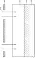
도 1 내지 도 8은 일 예에 따른 미세 패턴 형성 방법을 보여주는 단면도들이다.FIGS. 1 to 8 are cross-sectional views illustrating a method of forming a fine pattern according to an example.
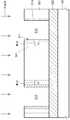
도 1은 레지스트층(300)에 노광 과정을 수행하는 단계를 보여준다.FIG. 1 shows a step of performing an exposure process on the
도 1을 참조하면, 반도체 기판과 같은 공정 과정이 수행될 기판(100) 상에 식각이 수행될 대상층으로 하부층(200)을 형성한다. 하부층(200) 상에 레지스트 물질을 도포하고 소프트 베이크(soft bake)하여 레지스트층(300)을 형성한다. 레지스트 물질을 도포하기 이전에 하부층(200) 표면을 표면 처리하는 과정을 더 수행할 수 있다. 예컨대, 헥사메틸디실라잔(HMDS: HexaMethylDiSilazane)과 같은 실라잔 가스를 이용하여 하부층(200)의 표면을 소수성으로 바꿔줘 레지스트층(300)과의 접착력을 개선할 수 있다. 노광 과정에서의 난반사를 억제하고 노광 정밀성을 개선하기 위해서, 바닥반사방지층(BARC: Bottom Anti-Reflective Coating: 도시되지 않음)을 레지스트층(300)의 하부에 더 형성할 수 있다. 바닥반사방지층은 유기물 또는 비유기물의 ARC를 포함할 수 있다. 레지스트층(300)을 형성한 후 레지스트층(300) 상에 상측 코팅층(top coat layer: 도시되지 않음)을 더 형성할 수도 있다.Referring to FIG. 1, a
레지스트층(300)이 형성된 기판(100)에 포토리소그래피(photolithography) 과정을 따르는 노광(exposure) 과정을 수행한다. 예컨대, 레지스트층(300) 상에 포토 마스크(photomask: 400)를 도입하고 노광 광(410)을 레지스트층(300)의 일부 영역에 조사할 수 있다. 이때, 노광 광(410)은 다양한 광원, 예컨대, ArF 광원에 의해 제공될 수 있다. 경우에 따라 KrF 광원이 사용될 수도 있다. 포토 마스크(400)는 바이너리 마스크(binary mask) 형태 또는 위상반전마스크(phase shift mask)와 같은 투과형 마스크 형태로 도입될 수 있다. 또는 반사형 마스크로 포토 마스크(400)가 도입될 수도 있다.The
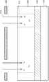
도 2는 노광된 제1영역(310)에 산(H+)들이 형성되는 현상을 보여준다.FIG. 2 shows the phenomenon that acids (H+ ) are formed in the exposed
도 2를 참조하면, 상에 포토 마스크(400)를 사용하는 노광 과정에 의해서, 레지스트층(300)의 노광 제1영역(310)이 노광 광(410)이 입사되어 노광될 수 있다. 노광에 의해 노광된 제1영역(310) 내에서 산(acid: H+)들이 발생될 수 있다. 레지스트층(300)은 화확증폭형 레지스트(CAR: Chemically Amplified Resist)를 포함하여 이루어질 수 있다. 입사되는 노광 광(410)은 화확증폭형 레지스트(CAR)에 함유된 광산발생제(PAG: Photo Acid Generator)가 산(acid: H+)들을 발생시키도록 유도한다. 노광된 제1영역(310)에 산들이 발생되어 노광된 제1영역(310)은 포토 마스크(400)에 형성된 패턴 이미지(pattern image)가 전사(transfer)된 잠상(latent image)이 형성될 수 있다.Referring to FIG. 2, the exposure
화학증폭형 레지스트(CAR)는 양자 수율이 100% 보다 큰 포토 레지스트 물질을 의미할 수 있으며, 프로텍팅-디프로테팅(protecting-deprotecting) 반응으로 노광된 부분과 비노광 부분 사이의 용해도의 차이를 제공하는 레지스트 물질일 수 있다. 화학증폭형 레지스트(CAR)는 매트릭스(matrix) 성분으로 폴리머(polymer)들을 포함하고, 폴리머들은 백본(backbone) 또는 주쇄(main chain)에 프로텍팅 그룹(protecting group)을 가질 수 있다. 폴리머 성분은 폴리하이드록시스티렌(PHS: PolyHydroxyStyrene) 폴리머를 포함할 수 있다. 프로텍팅 그룹은 t-부틸옥시카보닐(tert-Bulyloxycrbonyl: t-BOC)을 포함할 수 있다. 화학증폭형 레지스트는 콘트라스트(contrast)의 향상 또는 용해도의 조절, 산의 확산 정도를 제어 또는 조절하기 위해서 반응 금지제(inhibitor)를 더 포함할 수 있다.A chemically amplified resist (CAR) can refer to a photoresist material having a quantum yield of greater than 100%, and can be used to determine the difference in solubility between the exposed and unexposed portions in a protecting-deprotecting reaction Or the like. The chemically amplified resist (CAR) may include polymers as a matrix component, and the polymers may have a protecting group in a backbone or main chain. The polymer component may comprise a polyhydroxystyrene (PHS) polymer. The protecting group may include t-butyloxycarbonyl (t-BOC). The chemically amplified resist may further include an inhibitor to control or control the contrast enhancement or the control of the solubility or the acid diffusion.
레지스트층(300)을 이루는 화학증폭형 레지스트에 예컨대 엑시머 레이저(excimer laser)로부터 제공되는 노광 광(410)이 입사되는 노광에 의해서, PAG로부터 산이 발생되고 발생된 산이 확산할 수 있다. 노광된 레지스트층(300)에 노광 이후 이어지는 노광 후 베이크(PEB: Post Exposure Bake) 과정을 수행할 수 있다. 노광 후 베이크 과정은 대략 100℃ 내지 110℃의 온도 범위로 수행될 수 있다.An acid is generated from the PAG and the generated acid can be diffused by exposure in which the
노광 후 베이크에서 프로텍팅 그룹을 디프로텍팅시키는 반응이 유도될 수 있다. 프로텍팅 그룹은 t-BOC와 같이, 산(H+)들에 의해 제거될 수 있는 산에 불안정한 기 또는 그룹(acid labile group)을 포함할 수 있다. t-BOC와 같은 프로텍팅 그룹은 산(H+)과의 반응에 의해 수산화기(OH-)로 치환될 수 있다. t-BOC와 같은 프로텍팅 그룹은 폴리머의 주쇄 부분을 보호하여 지용성을 가지도록 유도하지만, 치환된 수산화기는 약 알칼리 용액일 수 있는 현상제(developer)에 대한 상대적 용해도가 높으므로, 이후의 제1현상 과정에 의해서 제1노광 영역(310)이 선택적으로 제거될 수 있다. 프로텍팅 그룹을 수산화기로 치환하는 디프로텍팅 반응으로 화학증폭형 레지스트의 노광 부분을 변성시킴으로써, 포토 마스크(400)에 구비된 패턴 이미지를 따르는 형상으로 제1노광 영역(310)을 변성시킬 수 있다.A reaction may be induced to deprotect the protecting group in the post-exposure bake. The protecting group may include an acid labile group that can be removed by acids (H+ ), such as t-BOC. Protecting groups such as t-BOC can be replaced with hydroxyl groups (OH- ) by reaction with acid (H+ ). Protecting groups such as t-BOC protect the main chain portion of the polymer to induce liposolubility, but since the substituted hydroxyl group has a high solubility in a developer which may be a weakly alkaline solution, The
PAG로부터 생성된 한 분자의 산(H+)이 확산되면서 촉매 반응을 통하여 디프로텍팅 반응, 즉, 탈 보호화 반응을 촉진시킬 수 있다. PEB의 온도와 시간에 따라 산의 확산이 증가되므로, 산의 확산을 조절하고 기타 오염에 따른 패턴의 불량을 억제하기 위해서 염기물을 반응 금지제(inhibitor)로 화학증폭형 레지스트는 더 포함할 수 있다. 화학증폭형 레지스트는 메타아클레이트(methacrylate) 폴리머와 같은 지방족(alicyclic) 폴리머나 COMA(cyclic olefin/maleic anhydride)와 같은 폴리머를 폴리머를 포함하여 이루어질 수 있다.The acid (H+ ) of one molecule generated from the PAG is diffused to promote the deprotecting reaction, that is, the deprotection reaction, through the catalytic reaction. Since diffusion of acid increases with temperature and time of PEB, it is possible to further include a chemically amplified resist as a reaction inhibitor in order to control diffusion of acid and to prevent defects in pattern due to other contamination have. The chemically amplified resist may comprise a polymer such as an alicyclic polymer such as a methacrylate polymer or a polymer such as a cyclic olefin / maleic anhydride (COMA).
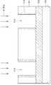
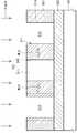
도 3은 제1오프닝 형상(opening feature: 510)을 제공하는 레지스트 제1패턴(301)을 형성하는 단계를 보여준다.FIG. 3 shows the step of forming a
도 3을 참조하면, 디프로텍팅 반응에 의한 탈 보호화 작용에 의해서 알칼리 용액에 대한 용해도가 상대적으로 증가된 노광 제1영역(도 2의 310)을 선택적으로 제거하는 제1현상 과정을 수행한다. 알칼리 현상제를 이용하여 노광 제1영역(310)을 현상 제거하여 제1오프닝 형상(510)이 하부의 하부층(200) 표면을 노출하는 레지스트 제1패턴(301)을 형성한다. 알칼리 현상제는 전형적인 포지티브 현상제(positive tone developer)로 도입될 수 있다. 예컨대, 2.38%의 수산화테트라메틸암모늄(TMAH: Tetramethyl Ammonium Hydroxide) 수용액 현상제를 사용하여 제1현상 과정을 수행할 수 있다.Referring to FIG. 3, a first development process is performed to selectively remove the first exposure region 310 (FIG. 2) in which the solubility of the alkali solution is relatively increased by the deprotecting action due to the deprotonating reaction. The
제1현상 과정으로 패터닝된 레지스트 제1패턴(301)은 포토 마스크(도 2의 400)에 형성된 패턴의 이미지가 전사된 형상으로 제1오프닝 형상(510)들을 제공하는 포지티브 패턴(positive pattern)으로 형성될 수 있다. 제1오프닝 형상(510)의 측벽 부분(314)에는 노광 제1영역(310)을 제거함에 의해 노출되는 측벽 표면을 가지고 노광 제1영역(310)으로부터 확산된 산(H+)들이 일부 잔류할 수 있다.The first resist
도 4 및 도 5는 노광된 제1영역(310)에서의 산(H+)들의 분포를 보여준다.Figures 4 and 5 show the distribution of the acids (H+ ) in the exposed
도 4를 참조하면, 노광 및 노광 후 베이크 과정에서 발생 및 확산된 산(H+)들은 노광 제1영역(310) 내에 분포될 수 있다. 산(H+)들은 노광 제1영역(310)에 입사되는 노광 광(410)에 의해 PAG로부터 발생되고 확산될 수 있다. 또한, 산(H+)들은 노광 후 베이크 과정에서 탈 보호화를 위한 디프로텍팅 반응에 참여하고 확산될 수 있다. 산(H+)들은 분포 곡선(309)로 보여지듯이 대부분 노광 제1영역(310) 내에 분포되고 있지만, 일부(309R)는 노광 제1영역(310)에 인근하는 제1오프닝 형상(도 3의 510)의 측벽 부분(314)로 확산 분포될 수 있다. 도 5에 제시된 바와 같이 노광 제1영역(310)에 인근하는 측벽 부분(314)에도 산(H+)들이 일부 잔류하는 상태가 얻어질 수 있으므로, 도 3에 제시된 바와 같이, 노광 제1영역(310)이 제1현상 제거되면서도 제1오프닝 형상(도 3의 510)의 측벽 부분(314)에는 산(H+)들이 일부 잔류할 수 있다. 제1오프닝 형상(도 3의 510)의 측벽 부분(314)에 잔류하는 산(H+)들은 노광 제1영역(310)에 분포하는 산(H+)에 비해 상대적으로 작은 량 또는 낮은 농도일 수 있어, 측벽 부분(314)은 제1현상에 의해 용해되어 제거되지 않고 잔류할 수 있다.Referring to FIG. 4, the acid (H +) generated and diffused in the exposure and post-exposure baking process may be distributed in the exposure
도 6 및 도 7은 산(H+)들이 확산된 제2영역(340)을 형성하는 단계를 보여준다.6 and 7 illustrate the step of forming a second region 340 in which the acids H+ are diffused.
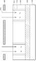
도 6을 참조하면, 제1오프닝 형상(510)을 제공하는 레지스트 제1패턴(301)을 형성된 결과물에 대해 어닐링(annealing)을 수행하여, 레지스트 제1패턴(301)의 측벽 부분(314)에 잔류하는 산(H+)들을 내측으로 확산(diffusion)하는 현상을 유도한다. 어닐링에 의해 인가되는 열에 의해서 레지스트 제1패턴(301)의 측벽 부분(314)에 잔류하는 산(H+)들은 제1오프닝 형상(510)의 측벽 표면(511)에 반대되는 방향인 레지스트 제1패턴(301)의 내측 방향으로 확산되어 확산 영역(341)을 형성할 수 있다. 레지스트 제1패턴(301)의 내측에 형성되는 확산 영역(341)은 어닐링이 진행되는 동안 점차 더 내측으로 확장될 수 있다. 확산 영역(341)을 확장시켜, 도 7에 제시된 바와 같이, 레지스트 제1패턴(301)의 가운데 중앙 부분에까지 산(H+)들의 확산이 미치지 못하여 중앙 부분이 산들의 확산이 미치지 않은 제3영역(311)들로 형성되도록 어닐링 과정을 수행할 수 있다. 산(H+)들의 확산에는 어닐링 시의 온도, 시간, 레지스트 제1패턴(301) 내에 함유된 반응 금지제의 함량 등이 영향을 미칠 수 있다. 따라서, 어닐링 시간을 조절하거나 또는 온도, 반응 금지제로서의 염기물의 첨가량을 조절함으로써, 레지스트 제1패턴(301) 내의 제3영역(311) 및 제2영역(340)의 선폭 크기를 제어할 수 있다.Referring to FIG. 6, the resist
레지스트 제1패턴(301)의 제2영역(340, 341) 내로 확산되는 산(H+)들은, 제2영역(340, 341) 내로 확산되고 또한 제2영역(340, 341) 내의 폴리머 성분에 구비된 프로텍팅 그룹을 디프로텍팅(deprotecting)하는 탈 보호화 작용을 유도할 수 있다. 이러한 탈 보호화 작용에 의해서 레지스트 제1패턴(301)의 제2영역(340, 341) 내의 폴리머 성분은 알칼리 현상제(alkaline developer)에 대한 용해도가 증가하며 또한 유기 용매에 대해 내성을 가져 저항성(resistance to organic solvent)을 가지도록 변성될 수 있다. 레지스트 제1패턴(301)의 제3영역(311)은 산(H+)의 확산이 미치지 못한 영역으로, 제3영역(311) 내의 레지스트 물질은 폴리머가 프로텍팅 그룹에 의해 보호되고 있는 상태, 즉, 알칼리 용액에 대한 내성을 가지나 유기 용매에 대한 상대적 용해도가 제2영역(340, 341) 보다는 큰 상태로 유지될 수 있다. 레지스트 제1패턴(301)의 제2영역(340, 341)은 디프로텍팅 반응에 의해 알칼리 용액에 대한 용해도가 증가하여, 상대적으로 유기 용매에 대한 용해도 제3영역(311) 보다 낮아진 상태로 변성될 수 있다. 이에 따라, 레지스트 제1패턴(301)의 제2영역(340, 341)과 제3영역(311)은 유기 용매에 대한 용해도가 서로 다른 상태를 가질 수 있다. 레지스트 제1패턴(301)의 제2영역(340, 341)은 제3영역(311)의 유기 용매에 대한 용해도 보다 낮은 유기 용매에 대한 용해도를 가질 수 있다. 이러한 유기 용매에 대한 용해도 차이를 유도함으로써, 후속 과정에서 별도의 추가적인 노광 과정을 도입하지 않고서도 제2현상 과정을 수행할 수 있다.The acids H+ diffused into the
어닐링 과정은 노광 후 베이크 과정에 설정된 베이크 온도 보다 높은 확산 온도로 수행될 수 있다. 어닐링 온도는 베이크 온도와 유사한 온도로 설정될 수도 있으나, 베이크 온도로 설정된 어닐링 과정에서 산(H+)들의 확산 거리는 상대적으로 낮게 제한되는 제약이 수반될 수 있다. 산(H+)들의 확산 거리를 보다 길게 하고 또한 산(H+)들의 확산 속도를 보다 빠르게 유도하기 위해서, 어닐링 온도로 설정되는 확산 온도는 베이크 온도 보다 높은 온도, 예컨대, 베이크 온도 보다 20℃ 내지 30℃ 높은 온도로 설정될 수 있다. 어닐링 시 확산 온도는 120℃ 내지 140℃ 온도로 설정될 수 있다. 어닐링 시 확산 온도는 폴리머 성분의 유리전이 온도(Tg)와 유사한 온도 범위로 설정될 수도 있다. 폴리머 성분의 백본(back bone)의 유리 전이 온도(Tg)는 대략 110℃ 내지 130℃일 수 있으며, 어닐링 시 확산 온도는 이러한 유리전이 온도(Tg)와 유사한 온도 범위로 설정될 수도 있다. 이러한 경우, 산(H+)들의 확산 시 레지스트 플로우(resist flow)를 수반하여 확산을 보다 효율적으로 유도할 수 있다.The annealing process can be performed at a diffusion temperature higher than the bake temperature set in the post-exposure bake process. The annealing temperature may be set to a temperature similar to the bake temperature, but the diffusion distance of the acids (H+ ) in the annealing process set to the bake temperature may be constrained to be relatively low. Longer than the diffusion length of the acid (H+) and also in order to more quickly lead to the diffusion rate of the acid (H+), the diffusion temperature is set to the annealing temperature is 20 ℃ to a higher temperature than the baking temperature, for example, baking temperature The temperature can be set to a high temperature of 30 [deg.] C. The diffusion temperature at the time of annealing may be set to a temperature of 120 캜 to 140 캜. The diffusion temperature at annealing may be set to a temperature range similar to the glass transition temperature (Tg) of the polymer component. The glass transition temperature (Tg) of the back bone of the polymer component may be approximately 110 ° C to 130 ° C, and the diffusion temperature at annealing may be set to a temperature range similar to this glass transition temperature (Tg). In this case, diffusion of acids (H+ ) can be accompanied by a resist flow to more effectively induce diffusion.
도 8은 제1오프닝 형상(510) 및 제2오프닝 형상(511)을 제공하는 레지스트 제2패턴(340P)을 형성하는 단계를 보여준다.FIG. 8 shows the step of forming a second resist
도 8을 참조하면, 레지스트 제1패턴(도 7의 301)의 제3영역(도 7의 311)을 선택적으로 제거하는 제2현상 과정을 수행한다. 레지스트 제1패턴(301)의 제2영역(도 7의 340)은 산(H+)에 의한 디프로텍팅 반응의 탈 보호화 작용에 의해서 알칼리 용액에 대한 용해도가 상대적으로 증가되고, 제3영역(311) 보다 유기 용매에 대한 용해도가 낮은 상태로 변성된 상태일 수 있다. 레지스트 제1패턴(310)의 제2영역(340)과 제3영역(311)의 유기 용매에 대한 용해도 차이를 이용하여, 제3영역(311)을 선택적으로 제2현상하여 제2오프닝 형상(511)들을 형성한다. 제2현상은 유기 용매(organic solvent)를 포함하는 유기 현상제를 사용하여 수행될 수 있다. 예컨대, 아세테이트, 알코올, 에테르, 에스테르 또는 케톤을 포함하는 유기 용매를 사용하여 레지스트 제1패턴(301)의 제3영역(311)을 선택적으로 용해 현상할 수 있다.Referring to FIG. 8, a second developing process for selectively removing the third region (311 in FIG. 7) of the resist first pattern (301 in FIG. 7) is performed. The second region (340 in FIG. 7) of the resist
제2현상에서 레지스트 제1패턴(301)의 제3영역(311)이 제거되며, 제3영역(311) 위치에 제2오프닝 형상(511)들이 제공되는 레지스트 제2패턴(340P)가 패터닝될 수 있다. 레지스트 제1패턴(301)의 제2영역(340)은 어닐링에 의한 산(H+)의 확산에 의해 그 영역의 폭이 설정되고, 제1오프닝 형상(510)들의 측벽 부분(도 7의 341)들로부터 산(H+)들이 서로 마주보는 방향으로 확산되므로, 양측의 제1오프닝 형상(510)들로부터 실질적으로 등간격을 가지는 중간 부분에 제2오프닝 형상(511)이 위치할 수 있다. 레지스트 제1패턴(301)의 제3영역(311)을 노광하는 과정없이 산(H+)의 확산과 유기 현상제를 이용한 제2현상으로 제2오프닝 형상(511)을 형성할 수 있다. 레지스트 제1패턴(301)의 제3영역(311)을 노광하는 과정없이 제2오프닝 형상(511)이 형성될 수 있으므로, 별도의 정렬 과정없이 제2오프닝 형상(511)이 제1오프닝 형상(510)들 사이의 중간 부분이 정렬되도록 위치할 수 있다. 따라서, 더블 패터닝이나 스페이서 패터닝 기술들에서와 같이 복수의 노광 과정들 사이에서 요구되는 정밀한 정렬 과정이 생략될 수 있다.The third region 311 of the resist
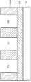
도 10 및 도 11은 일 예에 따른 미세 패턴 형성 방법의 어닐링 단계를 보여준다.10 and 11 show an annealing step of the method for forming a fine pattern according to an example.
도 10 및 도 11을 참조하면, 제1오프닝 형상(510)을 제공하는 레지스트 제1패턴(301)을 형성된 결과물에 대해 어닐링을 수행하기 이전에, 레지스트 제1패턴(301)의 측벽 표면(511)을 덮는 확산 촉진층(diffusion promotion layer: 650)을 더 형성할 수 있다. 확산 촉진층(650)은 레지스트 제1패턴(301)의 측벽 부분(314)에 잔류하는 산(H+)들을 내측으로 확산(diffusion)하는 현상을 상대적으로 더 활발히 촉진되는 현상을 유도하기 위해서 도입될 수 있다. 확산 촉진층(650)이 레지스트 제1패턴(301)을 덮도록 형성된 상태에서 어닐링을 수행하여 잔류하는 산(H+)들을 확산시킬 수 있다.10 and 11, a resist
확산 촉진층(650)은 pH 7 보다 낮은 산성도를 가지는 층으로 도입될 수 있다. 확산 촉진층(650)은 pH 7 보다 낮은 산성도를 가지는 수용성 폴리머를 코팅(coating)하여 형성될 수 있다. 확산 촉진층(650)은 pH 7 보다 낮은 산성도를 가지는 평균 무게 분자량(Mw)이 8000 이하의 폴리머를 코팅(coating)하여 형성될 수 있다. 확산 촉진층(650)은 산성의 환경을 제공하여, 레지스트 제1패턴(301)의 측벽 부분(314)에 잔류하는 산(H+)들이 표면(511) 외측으로 확산되는 것을 억제하여 표면(511)과 반대 방향으로 산(H+)들이 보다 더 확산되도록 유도할 수 있다. 이에 따라, 산(H+)들의 확산 거리를 증가시키고 확산 속도를 보다 더 높일 수 있다.The
도 12 내지 도 16은 다른 일 예에 따른 미세 패턴 형성 방법을 보여준다.12 to 16 show a method of forming a fine pattern according to another example.
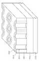
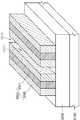
도 12 및 도 13은 제1오프닝 홀 형상(opening hole feature: 2510)을 제공하는 레지스트 제1패턴(2301)을 형성하는 단계를 보여준다.FIGS. 12 and 13 show steps of forming a resist
도 12를 참조하면, 반도체 기판(2100) 상에 식각이 수행될 대상층으로 하부층(2200)을 형성한다. 하부층(2200) 상에 레지스트 물질을 도포하고 소프트 베이크(soft bake)하여 레지스트층을 형성하고, 노광(exposure) 과정을 수행하고, 노광 제1영역을 선택적으로 제거하는 제1현상 과정을 수행한다. 알칼리 현상제를 이용하여 노광 제1영역을 현상 제거하여 제1오프닝 홀 형상(2510)들이 하부의 하부층(2200) 표면을 노출하는 레지스트 제1패턴(2301)을 형성한다.Referring to FIG. 12, a
제1현상 과정으로 패터닝된 레지스트 제1패턴(2301)은 포토 마스크에 형성된 패턴의 이미지가 전사된 형상으로 제1오프닝 홀 형상(2510)들을 제공하는 포지티브 패턴으로 형성될 수 있다. 도 13에 제시된 바와 같이, 제1오프닝 홀 형상(2510)의 측벽 부분(2314)에는 노광 제1영역을 제거함에 의해 노출되는 측벽 표면을 가지고 노광 제1영역으로부터 확산된 산(H+)들이 일부 잔류할 수 있다. 제1오프닝 홀 형상(2510)의 측벽 부분(2314)에 잔류하는 산(H+)들은 노광 제1영역에 분포된 산(H+)들에 비해 상대적으로 작은 량 또는 낮은 농도일 수 있어, 측벽 부분(2314)은 제1현상에 의해 용해되어 제거되지 않고 잔류할 수 있다.The resist
도 14 및 도 15는 산(H+)들이 확산된 제2영역(2340)을 형성하는 단계를 보여준다.Figs. 14 and 15 show the step of forming a
도 14를 참조하면, 제1오프닝 홀 형상(2510)을 제공하는 레지스트 제1패턴(2301)을 형성된 결과물에 대해 어닐링을 수행하여, 레지스트 제1패턴(2301)의 측벽 부분(2314)에 잔류하는 산(H+)들을 내측으로 확산하는 현상을 유도한다. 어닐링에 의해 인가되는 열에 의해서 레지스트 제1패턴(2301)의 측벽 부분(2314)에 잔류하는 산(H+)들은 제1오프닝 홀 형상(2510)의 측벽 표면에 반대되는 방향인 레지스트 제1패턴(2301)의 내측 방향으로 확산되어 확산 영역(2341)을 형성할 수 있다. 레지스트 제1패턴(2301)의 내측에 형성되는 확산 영역(2341)은 어닐링이 진행되는 동안 점차 더 내측으로 확장될 수 있다. 확산 영역(2341)을 계속 확장시켜 확산 영역(2341)들의 외측 경계가 상호 간에 맞닿도록 유도한다. 서로 다른 이격된 제1오프닝 홀 형상(2510)들로부터 확장되는 확산 영역(2341)들은 계속 확산되어 그 영역을 확장하면, 도 15에 제시된 바와 같이, 확산 영역(도 14의 2341)들이 상호 맞닿아 연결된 제2영역(2340)들이 설정될 수 있다. 제2영역(2340)은 제1오프닝 홀 형상(2510)들 사이의 중앙 부분의 레지스트 제1패턴(2301) 부분에 산(H+)들의 확산이 미치지 않은 제3영역(2311)들이 설정되도록 유도될 수 있다. 제2영역(2340)은 레지스트 제1패턴(2301)의 가운데 중앙 부분, 즉, 이웃하는 네 개의 제1오프닝 홀 형상(2510)들의 사이 가운데 중앙 부분이 산(H+)들의 확산이 미치지 않은 제3영역(2311)으로 설정되도록 형성될 수 있다. 또는, 제2영역(2340)은 레지스트 제1패턴(2301)의 이웃하는 세 개의 제1오프닝 홀 형상(2510)들 사이 가운데 중앙 부분이 산(H+)들의 확산이 미치지 않은 제3영역(2311)으로 설정되도록 형성될 수 있다. 제3영역(2311)은 제2영역(2340)에 에워싸인 고립된 섬(isolated island) 형상으로 설정될 수 있다.Referring to FIG. 14, a resist
레지스트 제1패턴(2301)의 제2영역(2340, 2341) 내로 확산되는 산(H+)들은, 제2영역(2340, 2341) 내로 확산되고 또한 제2영역(2340, 2341) 내의 폴리머 성분에 구비된 프로텍팅 그룹을 디프로텍팅하는 탈 보호화 작용을 유도할 수 있다. 이러한 탈 보호화 작용에 의해서 레지스트 제1패턴(2301)의 제2영역(2340, 2341) 내의 폴리머 성분은 알칼리 현상제에 대한 용해도가 증가하며 유기 용매에 대해 내성을 가져 저항성(resistance to organic solvent)을 가지도록 변성될 수 있다. 레지스트 제1패턴(2301)의 제3영역(2311)은 산(H+)의 확산이 미치지 못한 영역으로, 제3영역(2311) 내의 레지스트 물질은 폴리머가 프로텍팅 그룹에 의해 보호되고 있는 상태, 즉, 알칼리 용액에 대한 내성을 가지나 유기 용매에 대한 상대적 용해도가 제2영역(2340, 2341) 보다는 큰 상태로 유지될 수 있다.The acids H+ diffused into the
레지스트 제1패턴(2301)의 제3영역(2311)을 설정하도록 제2영역(2340)을 산(H+)의 확산을 통해 형성하는 어닐링 과정은, 도 9를 참조하여 설명한 바와 같은 산성 분위기 가스를 사용하는 어닐링 과정을 적용하여 수행될 수 있다. 레지스트 제1패턴(2301)의 제3영역(2311)을 설정하도록 제2영역(2340)을 산(H+)의 확산을 통해 형성하는 어닐링 과정은, 도 10 및 도 11을 참조하여 설명한 바와 같은 산성의 확산 촉진층(도 11의 650)을 적용한 어닐링 과정으로 수행될 수 있다.The annealing process for forming the
도 16은 제1오프닝 홀 형상(2510) 및 제2오프닝 홀 형상(2511)을 제공하는 레지스트 제2패턴(2340P)을 형성하는 단계를 보여준다.Figure 16 shows the step of forming a second resist
도 16을 참조하면, 레지스트 제1패턴(도 15의 2301)의 제3영역(도 15의 2311)을 선택적으로 제거하는 제2현상 과정을 수행한다. 레지스트 제1패턴(2301)의 제2영역(도 15의 2340)은 산(H+)에 의한 디프로텍팅 반응의 탈 보호화 작용에 의해서 알칼리 용액에 대한 용해도가 상대적으로 증가되고, 제3영역(2311) 보다 유기 용매에 대한 용해도가 낮은 상태로 변성된 상태일 수 있다. 레지스트 제1패턴(2310)의 제2영역(2340)과 제3영역(2311)의 유기 용매에 대한 용해도 차이를 이용하여, 제3영역(2311)을 선택적으로 제2현상하여 제2오프닝 홀 형상(2511)들을 형성한다. 제2현상은 유기 용매(organic solvent)를 포함하는 유기 현상제를 사용하여 수행될 수 있다. 예컨대, 아세테이트, 알코올, 에테르, 에스테르 또는 케톤을 포함하는 유기 용매를 사용하여 레지스트 제1패턴(2301)의 제3영역(2311)을 선택적으로 용해 현상할 수 있다.Referring to FIG. 16, a second developing process for selectively removing the third region 2311 (FIG. 15) of the resist first pattern 2301 (FIG. 15) is performed. The solubility in the alkali solution is relatively increased due to the deprotecting action of the difluorinating reaction by the acid (H+ ), and the second region (2340 of FIG. 15) 2311) may be in a state in which the solubility of the organic solvent is lowered. The
제2현상에서 레지스트 제1패턴(2301)의 제3영역(2311)이 제거되며, 제3영역(2311) 위치에 제2오프닝 홀 형상(2511)들이 제공되는 레지스트 제2패턴(2340P)가 패터닝될 수 있다. 제1오프닝 홀 형상(2510)들은 제2오프닝 홀 형상(2511)을 중앙 부분에 두고 제2오프닝 홀 형상(2511)을 4개의 제1오프닝 홀 형상(2510)들이 에워싸도록 배치될 수 있다. 또는, 제1오프닝 홀 형상(2510)들은 제2오프닝 홀 형상(2511)을 중앙 부분에 두고 제2오프닝 홀 형상(2511)을 3개의 제1오프닝 홀 형상(2510)들이 에워싸도록 배치될 수 있다. 또는, 제1오프닝 홀 형상(2510)들은 제2오프닝 홀 형상(2511)을 중앙 부분에 두고 제2오프닝 홀 형상(2511)을 네 개보다 더 많은 다수의 제1오프닝 홀 형상(2510)들이 에워싸도록 배치될 수 있다.The
도 17 내지 도 19는 다른 일 예에 따른 미세 패턴 형성 방법을 보여준다.17 to 19 show a method of forming a fine pattern according to another example.
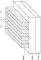
도 17은 제1오프닝 트렌치 형상(opening trench feature: 3510)을 제공하는 레지스트 제1패턴(3301)을 형성하는 단계를 보여준다.FIG. 17 shows the step of forming a resist
도 17을 참조하면, 반도체 기판(3100) 상에 하부층(3200)을 형성한다. 하부층(200) 상에 레지스트 물질을 도포하고 소프트 베이크(soft bake)하여 레지스트층을 형성하고, 노광(exposure) 과정을 수행하고, 노광 제1영역을 선택적으로 제거하는 제1현상 과정을 수행한다. 알칼리 현상제를 이용하여 노광 제1영역을 현상 제거하여 제1오프닝 트렌치 형상(3510)들이 하부의 하부층(3200) 표면을 노출하는 레지스트 제1패턴(3301)을 형성한다. 레지스트 제1패턴(3301)는 제1오프닝 트렌치 형상(3510)들이 일 방향으로 길게 연장되는 라인(line) 형상을 가지도록 라인 형상 또는 밴드 형상을 가지는 패턴으로 형성될 수 있다.Referring to FIG. 17, a
제1현상 과정으로 패터닝된 레지스트 제1패턴(3301)은 포토 마스크에 형성된 패턴의 이미지가 전사된 형상으로 제1오프닝 트렌치 형상(3510)들을 제공하는 포지티브 패턴으로 형성될 수 있다. 제1오프닝 트렌치 형상(3510)의 측벽(3511) 부분에는 노광 제1영역을 제거함에 의해 노출되는 측벽(3511) 표면을 가지고 노광 제1영역으로부터 확산된 산(H+)들이 일부 잔류할 수 있다.The first resist
도 18은 산(H+)들이 확산된 제2영역(3340)을 형성하는 단계를 보여준다.FIG. 18 shows the step of forming a
도 18을 참조하면, 제1오프닝 트렌치 형상(3510)을 제공하는 레지스트 제1패턴(3301)을 형성된 결과물에 대해 어닐링을 수행하여, 레지스트 제1패턴(3301)의 측벽(3511) 부분에 잔류하는 산(H+)들을 내측으로 확산하는 현상을 유도한다. 어닐링에 의해 인가되는 열에 의해서 레지스트 제1패턴(3301)의 측벽(3511) 부분에 잔류하는 산(H+)들은 제1오프닝 트렌치 형상(3510)의 측벽(3511) 표면에 반대되는 방향인 레지스트 제1패턴(3301)의 내측 방향으로 확산되어 확산 영역인 제2영역(3340)을 형성할 수 있다. 레지스트 제1패턴(3301)의 내측에 형성되는 확산 제2영역(3340)은 어닐링이 진행되는 동안 점차 더 내측으로 확장될 수 있다. 확산 제2영역(3340)을 계속 확장시켜 제2영역(3340)들 사이에 라인 형상의 제3영역(3311)이 산(H+)들이 확산되지 않은 영역을 설정할 수 있다. 제2영역(3340)은 제1오프닝 트렌치 형상(3510)들 사이의 중앙 부분의 레지스트 제1패턴(3301) 부분에 산(H+)들의 확산이 미치지 않은 제3영역(3311)들이 설정되도록 유도될 수 있다.18, the resist
레지스트 제1패턴(3301)의 제2영역(3340) 내로 확산되는 산(H+)들은, 제2영역(3340) 내로 확산되고 또한 제2영역(3340) 내의 폴리머 성분에 구비된 프로텍팅 그룹을 디프로텍팅하는 탈 보호화 작용을 유도할 수 있다. 이러한 탈 보호화 작용에 의해서 레지스트 제1패턴(3301)의 제2영역(3340) 내의 폴리머 성분은 알칼리 현상제에 대한 용해도가 증가하며 유기 용매에 대해 내성을 가져 저항성(resistance to organic solvent)을 가지도록 변성될 수 있다. 레지스트 제1패턴(3301)의 제3영역(3311)은 산(H+)의 확산이 미치지 못한 영역으로, 제3영역(3311) 내의 레지스트 물질은 폴리머가 프로텍팅 그룹에 의해 보호되고 있는 상태, 즉, 알칼리 용액에 대한 내성을 가지나 유기 용매에 대한 상대적 용해도가 제2영역(3340) 보다는 큰 상태로 유지될 수 있다.The acids H+ diffused into the
레지스트 제1패턴(3301)의 제3영역(3311)을 설정하도록 제2영역(3340)을 산(H+)의 확산을 통해 형성하는 어닐링 과정은, 도 9를 참조하여 설명한 바와 같은 산성 분위기 가스를 사용하는 어닐링 과정을 적용하여 수행될 수 있다. 레지스트 제1패턴(3301)의 제3영역(3311)을 설정하도록 제2영역(3340)을 산(H+)의 확산을 통해 형성하는 어닐링 과정은, 도 10 및 도 11을 참조하여 설명한 바와 같은 산성의 확산 촉진층(도 11의 650)을 적용한 어닐링 과정으로 수행될 수 있다.The annealing process for forming the
도 19는 제1오프닝 트렌치 형상(3510) 및 제2오프닝 트렌치 형상(3511)을 제공하는 레지스트 제2패턴(3340P)을 형성하는 단계를 보여준다.Figure 19 shows the step of forming a second resist
도 19를 참조하면, 레지스트 제1패턴(도 18의 3301)의 제3영역(도 18의 3311)을 선택적으로 제거하는 제2현상 과정을 수행한다. 레지스트 제1패턴(3301)의 제2영역(도 18의 3340)은 산(H+)에 의한 디프로텍팅 반응의 탈 보호화 작용에 의해서 알칼리 용액에 대한 용해도가 상대적으로 증가되고, 제3영역(3311) 보다 유기 용매에 대한 용해도가 낮은 상태로 변성된 상태일 수 있다. 레지스트 제1패턴(3310)의 제2영역(3340)과 제3영역(3311)의 유기 용매에 대한 용해도 차이를 이용하여, 제3영역(3311)을 선택적으로 제2현상하여 제2오프닝 트렌치 형상(3511)들을 형성한다. 제2현상은 유기 용매(organic solvent)를 포함하는 유기 현상제를 사용하여 수행될 수 있다. 예컨대, 아세테이트, 알코올, 에테르, 에스테르 또는 케톤을 포함하는 유기 용매를 사용하여 레지스트 제1패턴(3301)의 제3영역(3311)을 선택적으로 용해 현상할 수 있다.Referring to FIG. 19, a second developing process for selectively removing the third region (3311 in FIG. 18) of the resist first pattern (3301 in FIG. 18) is performed. The second region (3340 in FIG. 18) of the first pattern of resist 3301 has a relatively increased solubility in the alkali solution due to the deprotecting action of the difluorinating reaction by the acid (H+ ), 3311) may be in a state in which the solubility in an organic solvent is lowered. The
제2현상에서 레지스트 제1패턴(3301)의 제3영역(3311)이 제거되며, 제3영역(3311) 위치에 제2오프닝 트렌치 형상(3511)들이 제공되는 레지스트 제2패턴(3340P)가 패터닝될 수 있다. 제1오프닝 트렌치 형상(3510)들은 제2오프닝 홀 형상(3511)을 중앙 부분에 두도록 배치될 수 있다.The
본 출원에 따르면, 대면적의 기판 상에 한 번의 노광 과정 및 화학증폭형 레지스트 내에 잔류하는 산(H+)들의 확산, 서로 다른 제1 및 제2현상 과정들을 이용하여 노광 장비의 해상도 한계를 극복하여 나노 스케일(nanoscale) 크기의 구조물 또는 나노 구조체를 형성할 수 있다. 나노 구조체는, 선격자를 포함하는 편광판의 제조, 반사형 액정표시장치의 반사 렌즈의 형성 등에 이용할 수 있다. 나노 구조체는 독립적인 편광판의 제조에 사용될 뿐만 아니라, 표시 패널과 일체형인 편광부의 형성에도 이용할 수 있다. 예컨대, 박막 트랜지스터를 포함하는 어레이(array) 기판이나, 컬러필터 기판 상에 직접적으로 편광부를 형성하는 공정에 이용할 수 있다. 나노 구조체는 나노 와이어 트랜지스터, 메모리의 제작을 위한 주형, 나노 스케일의 도선 패터닝을 위한 나노 구조물과 같은 전기 전자 부품의 주형, 태양 전지와 연료 전지의 촉매 제작을 위한 주형, 식각 마스크와 유기 다이오드(OLED) 셀 제작을 위한 주형 및 가스 센서 제작을 위한 주형에 이용할 수 있다.The present application overcomes the resolution limitations of exposure equipment using a single exposure process on a large area substrate and the diffusion of acids (H+ ) remaining in the chemically amplified resist, different first and second development processes To form nanoscale-sized structures or nanostructures. The nanostructure can be used for the production of a polarizing plate including a line grating and the formation of a reflection lens of a reflection type liquid crystal display device. The nanostructure can be used not only for the production of independent polarizing plates but also for the formation of polarizing portions integral with the display panel. For example, it can be used for an array substrate including a thin film transistor or a process for forming a polarizing portion directly on a color filter substrate. The nanostructures can be used in various applications including nanowire transistors, templates for memory fabrication, molds for electrical and electronic components such as nanostructures for nanoscale patterning of leads, templates for catalysts for solar cells and fuel cells, etch masks and organic diodes ) Can be used for molds for making molds and gas sensors for cell fabrication.
상술한 본 출원에 따른 방법 들은 집적 회로 칩(integrated circuit chip) 제조에 사용될 수 있다. 결과의 집적 회로 칩은 웨이퍼 형태(raw wafer form)나 베어 다이(bare die) 또는 패키지 형태(package form)으로 제조자에 의해 배포될 수 있다. 칩은 단일 칩 패키지(single chip package)나 멀티칩 패키지 chip package) 형태로 제공될 수 있다. 또한, 하나의 칩은 다른 집적 회로 칩에 집적되거나 별도의 회로 요소(discrete circuit element)에 집적될 수 있다. 하나의 칩은 마더보드(mother board)와 같은 중간 제품(intermediate product)이나 최종 제제품(end product) 형태의 한 부품으로 다른 신호 프로세싱 소자(signal processing device)를 이루도록 집적될 수 있다. 최종 제품은 집적 회로 칩을 포함하는 어떠한 제품일 수 있으며, 장난감이나 저성능 적용 제품(application)으로부터 고성능 컴퓨터 제품일 수 있으며, 표시장치(display)나 키보드(keyboard) 또는 다른 입력 수단(input device) 및 중앙연산장치(central processor)를 포함하는 제품일 수 있다.The methods according to the present application described above can be used for the manufacture of integrated circuit chips. The resulting integrated circuit chip may be distributed by the manufacturer in a raw wafer form, a bare die, or a package form. The chip may be provided in the form of a single chip package or a multi-chip package chip package. In addition, one chip may be integrated into another integrated circuit chip or integrated into a discrete circuit element. One chip may be integrated to form another signal processing device as a part in the form of an intermediate product such as a mother board or an end product. The final product may be any product including an integrated circuit chip and may be a high performance computer product from a toy or low performance application and may be a display or keyboard or other input device, And a central processor.
상술한 바와 같이 본 출원의 실시 형태들을 도면들을 예시하며 설명하지만, 이는 본 출원에서 제시하고자 하는 바를 설명하기 위한 것이며, 세밀하게 제시된 형상으로 본 출원에서 제시하고자 하는 바를 한정하고자 한 것은 아니다. 본 출원에서 제시한 기술적 사상이 반영되는 한 다양한 다른 변형예들이 가능할 것이다.Although the embodiments of the present application as described above illustrate and describe the drawings, it is intended to illustrate what is being suggested in the present application and is not intended to limit what is presented in the present application in a detailed form. Various other modifications will be possible as long as the technical ideas presented in this application are reflected.
300: 레지스트층,310: 노광 제1영역,
311; 비확산 제3영역,340: 확산 제2영역.300: resist layer, 310: exposure first region,
311; Non-diffusing third region, 340: diffusing second region.
Claims (20)
Translated fromKorean상기 노광된 제1영역들을 제1현상하여 제1오프닝 홀(hole) 형상들을 제공하는 레지스트 제1패턴들을 형성하는 단계;
상기 레지스트 제1패턴들의 측벽 부분들에 잔존하는 상기 산들을 내측으로 확산(diffusion)하고 상기 산들이 확산된 제2영역들이 상호 맞닿도록 연장하여 중앙 부분에 상기 산들이 확산되지 못한 제3영역들을 고립된 섬(isolated island) 형상으로 형성하는 단계; 및
상기 제3영역들을 제2현상하여 상기 제1오프닝 홀 형상들로 둘러싸인 제2오프닝 홀 형상들을 제공하는 레지스트 제2패턴들을 패터닝하는 단계를 포함하는 미세 패턴 형성 방법.An exposure step of generating acids in first regions of a chemically amplified resist layer;
Forming first resist patterns that provide first opening hole shapes by first developing the exposed first areas;
Diffusion of the acids remaining in the sidewall portions of the first patterns of resist is extended inward so that the second regions of the acid diffused are mutually abutted and the third regions in which the acids are not diffused in the central portion are isolated Forming an island in an island shape; And
And patterning the resist second patterns to provide second opening hole shapes surrounded by the first opening hole shapes by second developing the third regions.
상기 노광 단계는
프로텍팅 그룹(protecting group)을 가지는 폴리머(polymer) 성분 및 광산발생제(PAG)를 포함하는 상기 화학증폭형 레지스트의 상기 광산발생제(PAG)가 상기 산들을 발생시키도록 유도하고,
상기 프로텍팅 그룹은 상기 산들에 의해 제거될 수 있는 산에 불안정한 그룹(acid labile)을 포함하고
상기 산들은 상기 프로텍팅 그룹을 디프로텍팅(deprotecting)하여 상기 폴리머 성분이 알칼리 현상제(alkaline developer)에 용해되도록 변성하고,
상기 노광 단계는 상기 산들이 상기 프로텍팅 그룹을 제거하는 작용에 영향을 미치도록 하는 노광후 베이크(post exposure baking) 단계를 수반하는 미세 패턴 형성 방법.The method according to claim 1,
The step of exposing
Wherein the photoacid generator (PAG) of the chemically amplified resist comprising a polymer component having a protecting group and a photoacid generator (PAG)
The protecting group comprises an acid labile group that can be removed by the acids
The acids deprotect the protecting group to denature the polymer component to be dissolved in an alkaline developer,
Wherein the step of exposing is accompanied by a post exposure baking step that causes the acids to affect the action of removing the protecting group.
상기 제1현상 단계는
상기 알칼리 현상제(alkaline developer)를 사용하여 상기 노광된 제1영역들의 제거를 유도하는 미세 패턴 형성 방법.3. The method of claim 2,
The first developing step
Wherein the exposure of the first regions is induced using the alkaline developer.
상기 알칼리 현상제(alkaline developer)는
2.38%의 수산화테트라메틸암모늄(TMAH: Tetramethyl Ammonium Hydroxide) 수용액 현상제를 포함하는 미세 패턴 형성 방법.The method of claim 3,
The alkaline developer may be
2.38% aqueous solution developer of tetramethyl ammonium hydroxide (TMAH).
상기 산들을 내측으로 확산(diffusion)하는 단계는
상기 노광후 베이크 단계에서 사용되는 베이크 온도 보다 높은 확산 온도로 상기 레지스트 제1패턴들을 어닐링(annealing)하는 단계를 포함하는 미세 패턴 형성 방법.3. The method of claim 2,
The step of diffusing the acids inward
And annealing the resist first patterns at a diffusion temperature higher than a bake temperature used in the post-exposure baking step.
상기 확산 온도는
상기 베이크 온도 보다 20℃ 내지 30℃ 높은 온도로 설정되는 미세 패턴 형성 방법.6. The method of claim 5,
The diffusion temperature
Wherein the baking temperature is set to a temperature higher than the baking temperature by 20 ° C to 30 ° C.
상기 확산 온도는
상기 120℃ 내지 140℃ 온도로 설정되는 미세 패턴 형성 방법.The method according to claim 6,
The diffusion temperature
Lt; RTI ID = 0.0 > 120 C < / RTI >
상기 어닐링(annealing)하는 단계는
상기 레지스트 제1패턴의 제2영역 내로 상기 산들을 확산시키고,
상기 확산된 산들이 상기 제2영역 내의 상기 프로텍팅 그룹을 디프로텍팅(deprotecting)하여 상기 제2영역 내의 상기 폴리머 성분이 알칼리 현상제(alkaline developer)에 용해될 수 있으나 유기 용매에 대해 내성을 가져 저항하도록(resistance to organic solvent) 변성되도록 유도하는 미세 패턴 형성 방법.6. The method of claim 5,
The step of annealing may comprise:
Diffusing the acids into a second region of the resist first pattern,
The diffused acids deprotect the protecting group in the second region so that the polymer component in the second region can be dissolved in the alkaline developer but is resistant to the organic solvent To a denatured resistivity to an organic solvent.
상기 제2현상 단계는
상기 유기 용매(organic solvent)를 사용하여 상기 제3영역들의 제거를 유도하는 미세 패턴 형성 방법.9. The method of claim 8,
The second developing step
And the removal of the third regions is induced by using the organic solvent.
상기 유기 용매(organic solvent)는
아세테이트, 알코올, 에테르, 에스테르 또는 케톤을 포함하는 미세 패턴 형성 방법.10. The method of claim 9,
The organic solvent may be, for example,
Acetate, alcohol, ether, ester or ketone.
상기 어닐링 단계 이전에
상기 레지스트 제1패턴의 측벽을 덮어 상기 산의 확산을 도와주는 산성의 확산 촉진층(diffusion promotion layer)를 형성하는 단계를 더 포함하는 미세 패턴 형성 방법.6. The method of claim 5,
Before the annealing step
And forming an acidic diffusion promotion layer to cover the sidewalls of the resist first pattern to assist diffusion of the acid.
상기 확산 촉진층은
산성의 폴리머를 포함하는 미세 패턴 형성 방법.12. The method of claim 11,
The diffusion promoting layer
A method for forming a fine pattern comprising an acidic polymer.
상기 어닐링 단계는
산성의 분위기 가스를 상기 레지스트 제1패턴들 상에 제공하는 단계를 포함하는 미세 패턴 형성 방법.6. The method of claim 5,
The annealing step
Providing an acidic atmosphere gas on the resist first patterns.
상기 산성의 분위기 가스는
염산(HCl) 가스를 포함하는 미세 패턴 형성 방법.14. The method of claim 13,
The acidic atmospheric gas
A method of forming a fine pattern comprising a hydrochloric acid (HCl) gas.
상기 제1오프닝 홀(hole) 형상들은
상기 제2오프닝 홀 형상을 중앙 부분에 두고 상기 제2오프닝 홀 형상을 4개의 상기 제1오프닝 홀 형상들이 에워싸도록 배치되는 미세 패턴 형성 방법.The method according to claim 1,
The first opening hole shapes
Wherein the second opening hole shape is disposed at a central portion and the second opening hole shape is disposed so as to surround the four first opening hole shapes.
상기 제1오프닝 홀(hole) 형상들은
상기 제2오프닝 홀 형상을 중앙 부분에 두고 상기 제2오프닝 홀 형상을 3개의 상기 제1오프닝 홀 형상들이 에워싸도록 배치되는 미세 패턴 형성 방법.The method according to claim 1,
The first opening hole shapes
Wherein the second opening hole shape is disposed at a central portion and the second opening hole shape is disposed so as to surround the three first opening hole shapes.
상기 노광된 제1영역들을 제1현상하여 레지스트 제1패턴들을 형성하는 단계;
상기 레지스트 제1패턴들의 측벽 부분들에 잔존하는 상기 산들을 내측으로 확산(diffusion)하여 상기 레지스트 제1패턴들에 상기 산들이 확산된 제2영역들 및 상기 산들이 확산되지 못한 제3영역들을 형성하는 단계; 및
상기 제3영역들을 제2현상하여 레지스트 제2패턴들을 패터닝하는 단계를 포함하는 미세 패턴 형성 방법.An exposure step of generating acids in first regions of a chemically amplified resist layer;
Developing the exposed first regions to form resist first patterns;
Diffusion of the acids remaining in the sidewall portions of the resist first patterns into the resist first patterns forms third regions in which the acids are diffused and third regions in which the acids are not diffused ; And
And patterning the resist second patterns by second developing the third regions.
상기 노광 단계는 노광후 베이크(post exposure baking) 단계를 수반하고,
상기 산들을 내측으로 확산(diffusion)하는 단계는,
상기 노광후 베이크 단계에서 사용되는 베이크 온도 보다 높은 확산 온도로 상기 레지스트 제1패턴들을 어닐링(annealing)하는 단계를 포함하는 미세 패턴 형성 방법.18. The method of claim 17,
The exposure step involves a post exposure baking step,
The step of diffusing the acids inward may include:
And annealing the resist first patterns at a diffusion temperature higher than a bake temperature used in the post-exposure baking step.
상기 제1현상 단계는
알칼리 현상제(alkaline developer)를 사용하여 수행되고,
상기 제2현상 단계는
상기 알칼리 현상제와 다른 다른 유기 용매(organic solvent)를 사용하여 수행되는 미세 패턴 형성 방법.18. The method of claim 17,
The first developing step
Is carried out using an alkaline developer,
The second developing step
Wherein the alkali developer is used in an organic solvent other than the alkali developer.
상기 노광된 제1영역들을 제1현상하여 제1오프닝 트렌치(trench) 형상들을 제공하는 레지스트 제1라인(line) 패턴들을 형성하는 단계;
상기 레지스트 제1라인 패턴들의 측벽 부분들에 잔존하는 상기 산들을 내측으로 확산(diffusion)하여 상기 산들이 확산된 제2영역들을 형성하고 상기 제2영역들 사이 중앙 부분에 상기 산들이 확산되지 못한 제3영역들을 라인 형상(line feature)으로 형성하는 단계; 및
상기 제3영역들을 제2현상하여 상기 제1오프닝 트렌치 형상들 사이에 제2오프닝 트렌치 형상들을 제공하는 레지스트 제2패턴들을 패터닝하는 단계를 포함하는 미세 패턴 형성 방법.An exposure step of generating acids in first regions of a chemically amplified resist layer;
Forming first resist line patterns that first develop the exposed first regions to provide first opening trench shapes;
The first resist patterns are formed by diffusing the acids remaining in the sidewall portions of the first line patterns to form second regions in which the acids are diffused, 3 regions as line features; And
And patterning resist second patterns for second development of the third regions to provide second opening trench shapes between the first opening trench shapes.
Priority Applications (2)
| Application Number | Priority Date | Filing Date | Title |
|---|---|---|---|
| KR1020150050478AKR20160121059A (en) | 2015-04-09 | 2015-04-09 | Method of forming fine patterns |
| US14/823,813US20160299427A1 (en) | 2015-04-09 | 2015-08-11 | Method of forming fine patterns |
Applications Claiming Priority (1)
| Application Number | Priority Date | Filing Date | Title |
|---|---|---|---|
| KR1020150050478AKR20160121059A (en) | 2015-04-09 | 2015-04-09 | Method of forming fine patterns |
Publications (1)
| Publication Number | Publication Date |
|---|---|
| KR20160121059Atrue KR20160121059A (en) | 2016-10-19 |
Family
ID=57111894
Family Applications (1)
| Application Number | Title | Priority Date | Filing Date |
|---|---|---|---|
| KR1020150050478AWithdrawnKR20160121059A (en) | 2015-04-09 | 2015-04-09 | Method of forming fine patterns |
Country Status (2)
| Country | Link |
|---|---|
| US (1) | US20160299427A1 (en) |
| KR (1) | KR20160121059A (en) |
Cited By (2)
| Publication number | Priority date | Publication date | Assignee | Title |
|---|---|---|---|---|
| WO2020102164A1 (en)* | 2018-11-13 | 2020-05-22 | Tokyo Electron Limited | Method for planarization of organic films |
| KR20220060264A (en)* | 2020-11-04 | 2022-05-11 | 엠에이치디 주식회사 | Method of forming fine patterns of semiconductor device |
Families Citing this family (2)
| Publication number | Priority date | Publication date | Assignee | Title |
|---|---|---|---|---|
| JP6684583B2 (en) | 2015-12-10 | 2020-04-22 | 東京応化工業株式会社 | Resist pattern formation method |
| KR102527708B1 (en)* | 2018-05-30 | 2023-05-02 | 삼성전기주식회사 | Fine dust concentration sensor |
Family Cites Families (2)
| Publication number | Priority date | Publication date | Assignee | Title |
|---|---|---|---|---|
| JP2008103384A (en)* | 2006-10-17 | 2008-05-01 | Elpida Memory Inc | Resist pattern forming method and resist applying developing apparatus |
| TWI584061B (en)* | 2014-08-27 | 2017-05-21 | 羅門哈斯電子材料有限公司 | Multiple-pattern forming methods |
- 2015
- 2015-04-09KRKR1020150050478Apatent/KR20160121059A/ennot_activeWithdrawn
- 2015-08-11USUS14/823,813patent/US20160299427A1/ennot_activeAbandoned
Cited By (3)
| Publication number | Priority date | Publication date | Assignee | Title |
|---|---|---|---|---|
| WO2020102164A1 (en)* | 2018-11-13 | 2020-05-22 | Tokyo Electron Limited | Method for planarization of organic films |
| US11393694B2 (en) | 2018-11-13 | 2022-07-19 | Tokyo Electron Limited | Method for planarization of organic films |
| KR20220060264A (en)* | 2020-11-04 | 2022-05-11 | 엠에이치디 주식회사 | Method of forming fine patterns of semiconductor device |
Also Published As
| Publication number | Publication date |
|---|---|
| US20160299427A1 (en) | 2016-10-13 |
Similar Documents
| Publication | Publication Date | Title |
|---|---|---|
| US9012132B2 (en) | Coating material and method for photolithography | |
| US7033735B2 (en) | Water soluble negative tone photoresist | |
| CN102074462B (en) | Method of Forming Electronic Devices | |
| US8043794B2 (en) | Method of double patterning, method of processing a plurality of semiconductor wafers and semiconductor device | |
| US20100273111A1 (en) | Dual tone development with plural photo-acid generators in lithographic applications | |
| TWI428958B (en) | Methods of forming photolithographic patterns | |
| US9257281B2 (en) | Methods of fabricating a pattern using the block co-polymer materials | |
| US8530147B2 (en) | Patterning process | |
| CN101963756A (en) | Form the method for electron device | |
| US8574810B2 (en) | Dual tone development with a photo-activated acid enhancement component in lithographic applications | |
| US9058997B2 (en) | Process of multiple exposures with spin castable films | |
| KR20160121059A (en) | Method of forming fine patterns | |
| US7662542B2 (en) | Pattern forming method and semiconductor device manufacturing method | |
| US7384725B2 (en) | System and method for fabricating contact holes | |
| CN108983546A (en) | Lithographic method | |
| Ronse et al. | Lithography options for the 32 nm half pitch node and beyond | |
| KR20130039124A (en) | Method for forming patterns of semiconductor device | |
| KR20150007921A (en) | Method of forming fine patterns for semiconductor device | |
| US8257911B2 (en) | Method of process optimization for dual tone development | |
| CN103000497B (en) | Method of forming an etch mask | |
| CN115868012A (en) | Method for forming narrow groove contact part | |
| JP2009139695A (en) | Manufacturing method of semiconductor device | |
| Ivan et al. | Photoimaging and lithographic processes in polymers | |
| CN100447672C (en) | Minute pattern photoetching method | |
| CN101510503A (en) | Pattern forming method, semiconductor device manufacturing method and semiconductor device manufacturing apparatus |
Legal Events
| Date | Code | Title | Description |
|---|---|---|---|
| PA0109 | Patent application | Patent event code:PA01091R01D Comment text:Patent Application Patent event date:20150409 | |
| PG1501 | Laying open of application | ||
| PC1203 | Withdrawal of no request for examination |