KR20160119889A - Semiconductor devices and methods of manufacturing semiconductor devices - Google Patents
Semiconductor devices and methods of manufacturing semiconductor devicesDownload PDFInfo
- Publication number
- KR20160119889A KR20160119889AKR1020150048181AKR20150048181AKR20160119889AKR 20160119889 AKR20160119889 AKR 20160119889AKR 1020150048181 AKR1020150048181 AKR 1020150048181AKR 20150048181 AKR20150048181 AKR 20150048181AKR 20160119889 AKR20160119889 AKR 20160119889A
- Authority
- KR
- South Korea
- Prior art keywords
- region
- regions
- source
- disposed
- concentration
- Prior art date
- Legal status (The legal status is an assumption and is not a legal conclusion. Google has not performed a legal analysis and makes no representation as to the accuracy of the status listed.)
- Granted
Links
Images


Classifications
- H—ELECTRICITY
- H10—SEMICONDUCTOR DEVICES; ELECTRIC SOLID-STATE DEVICES NOT OTHERWISE PROVIDED FOR
- H10D—INORGANIC ELECTRIC SEMICONDUCTOR DEVICES
- H10D30/00—Field-effect transistors [FET]
- H10D30/60—Insulated-gate field-effect transistors [IGFET]
- H10D30/62—Fin field-effect transistors [FinFET]
- H10D30/6219—Fin field-effect transistors [FinFET] characterised by the source or drain electrodes
- H01L29/785—
- H01L29/7848—
- H—ELECTRICITY
- H10—SEMICONDUCTOR DEVICES; ELECTRIC SOLID-STATE DEVICES NOT OTHERWISE PROVIDED FOR
- H10D—INORGANIC ELECTRIC SEMICONDUCTOR DEVICES
- H10D30/00—Field-effect transistors [FET]
- H10D30/01—Manufacture or treatment
- H10D30/021—Manufacture or treatment of FETs having insulated gates [IGFET]
- H10D30/024—Manufacture or treatment of FETs having insulated gates [IGFET] of fin field-effect transistors [FinFET]
- H—ELECTRICITY
- H10—SEMICONDUCTOR DEVICES; ELECTRIC SOLID-STATE DEVICES NOT OTHERWISE PROVIDED FOR
- H10D—INORGANIC ELECTRIC SEMICONDUCTOR DEVICES
- H10D30/00—Field-effect transistors [FET]
- H10D30/60—Insulated-gate field-effect transistors [IGFET]
- H10D30/62—Fin field-effect transistors [FinFET]
- H—ELECTRICITY
- H10—SEMICONDUCTOR DEVICES; ELECTRIC SOLID-STATE DEVICES NOT OTHERWISE PROVIDED FOR
- H10D—INORGANIC ELECTRIC SEMICONDUCTOR DEVICES
- H10D62/00—Semiconductor bodies, or regions thereof, of devices having potential barriers
- H10D62/10—Shapes, relative sizes or dispositions of the regions of the semiconductor bodies; Shapes of the semiconductor bodies
- H10D62/13—Semiconductor regions connected to electrodes carrying current to be rectified, amplified or switched, e.g. source or drain regions
- H10D62/149—Source or drain regions of field-effect devices
- H10D62/151—Source or drain regions of field-effect devices of IGFETs
- H—ELECTRICITY
- H10—SEMICONDUCTOR DEVICES; ELECTRIC SOLID-STATE DEVICES NOT OTHERWISE PROVIDED FOR
- H10D—INORGANIC ELECTRIC SEMICONDUCTOR DEVICES
- H10D62/00—Semiconductor bodies, or regions thereof, of devices having potential barriers
- H10D62/60—Impurity distributions or concentrations
- H—ELECTRICITY
- H10—SEMICONDUCTOR DEVICES; ELECTRIC SOLID-STATE DEVICES NOT OTHERWISE PROVIDED FOR
- H10D—INORGANIC ELECTRIC SEMICONDUCTOR DEVICES
- H10D62/00—Semiconductor bodies, or regions thereof, of devices having potential barriers
- H10D62/80—Semiconductor bodies, or regions thereof, of devices having potential barriers characterised by the materials
- H10D62/83—Semiconductor bodies, or regions thereof, of devices having potential barriers characterised by the materials being Group IV materials, e.g. B-doped Si or undoped Ge
- H10D62/832—Semiconductor bodies, or regions thereof, of devices having potential barriers characterised by the materials being Group IV materials, e.g. B-doped Si or undoped Ge being Group IV materials comprising two or more elements, e.g. SiGe
- H—ELECTRICITY
- H10—SEMICONDUCTOR DEVICES; ELECTRIC SOLID-STATE DEVICES NOT OTHERWISE PROVIDED FOR
- H10D—INORGANIC ELECTRIC SEMICONDUCTOR DEVICES
- H10D64/00—Electrodes of devices having potential barriers
- H10D64/20—Electrodes characterised by their shapes, relative sizes or dispositions
- H10D64/23—Electrodes carrying the current to be rectified, amplified, oscillated or switched, e.g. sources, drains, anodes or cathodes
- H10D64/251—Source or drain electrodes for field-effect devices
- H10D64/257—Source or drain electrodes for field-effect devices for lateral devices wherein the source or drain electrodes are characterised by top-view geometrical layouts, e.g. interdigitated, semi-circular, annular or L-shaped electrodes
- H—ELECTRICITY
- H10—SEMICONDUCTOR DEVICES; ELECTRIC SOLID-STATE DEVICES NOT OTHERWISE PROVIDED FOR
- H10D—INORGANIC ELECTRIC SEMICONDUCTOR DEVICES
- H10D64/00—Electrodes of devices having potential barriers
- H10D64/60—Electrodes characterised by their materials
- H10D64/62—Electrodes ohmically coupled to a semiconductor
- H01L2029/785—
- H—ELECTRICITY
- H10—SEMICONDUCTOR DEVICES; ELECTRIC SOLID-STATE DEVICES NOT OTHERWISE PROVIDED FOR
- H10B—ELECTRONIC MEMORY DEVICES
- H10B10/00—Static random access memory [SRAM] devices
- H10B10/12—Static random access memory [SRAM] devices comprising a MOSFET load element
- H—ELECTRICITY
- H10—SEMICONDUCTOR DEVICES; ELECTRIC SOLID-STATE DEVICES NOT OTHERWISE PROVIDED FOR
- H10D—INORGANIC ELECTRIC SEMICONDUCTOR DEVICES
- H10D30/00—Field-effect transistors [FET]
- H10D30/40—FETs having zero-dimensional [0D], one-dimensional [1D] or two-dimensional [2D] charge carrier gas channels
- H10D30/43—FETs having zero-dimensional [0D], one-dimensional [1D] or two-dimensional [2D] charge carrier gas channels having 1D charge carrier gas channels, e.g. quantum wire FETs or transistors having 1D quantum-confined channels
- H—ELECTRICITY
- H10—SEMICONDUCTOR DEVICES; ELECTRIC SOLID-STATE DEVICES NOT OTHERWISE PROVIDED FOR
- H10D—INORGANIC ELECTRIC SEMICONDUCTOR DEVICES
- H10D62/00—Semiconductor bodies, or regions thereof, of devices having potential barriers
- H10D62/10—Shapes, relative sizes or dispositions of the regions of the semiconductor bodies; Shapes of the semiconductor bodies
- H10D62/117—Shapes of semiconductor bodies
- H10D62/118—Nanostructure semiconductor bodies
- H10D62/119—Nanowire, nanosheet or nanotube semiconductor bodies
- H10D62/121—Nanowire, nanosheet or nanotube semiconductor bodies oriented parallel to substrates
Landscapes
- Insulated Gate Type Field-Effect Transistor (AREA)
Abstract
Translated fromKoreanDescription
Translated fromKorean본 발명은 반도체 장치 및 반도체 장치의 제조 방법에 관한 것이다.
The present invention relates to a semiconductor device and a manufacturing method of the semiconductor device.
반도체 장치에 대한 고성능, 고속화 및/또는 다기능화 등에 대한 요구가 증가되면서, 반도체 장치의 집적도가 증가되고 있다. 반도체 장치의 고집적화 경향에 대응한 미세 패턴의 반도체 소자를 제조하는 데 있어서, 미세한 폭 또는 미세한 이격 거리를 가지는 패턴들을 구현하는 것이 요구된다. 또한, 평면형(planar) MOSFET(metal oxide semiconductor FET)이 갖는 소자 특성의 한계를 극복하기 위하여, 3차원 구조의 채널을 구비하는 FinFET을 포함하는 반도체 장치를 개발하기 위한 노력이 진행되고 있다.
As the demand for high performance, high speed and / or multi-functionalization of semiconductor devices is increased, the degree of integration of semiconductor devices is increasing. In fabricating a semiconductor device having a fine pattern corresponding to a tendency toward high integration of a semiconductor device, it is required to realize patterns having a fine width or a small distance. Further, in order to overcome the limitations of device characteristics of a planar MOSFET (metal oxide semiconductor FET), efforts are being made to develop a semiconductor device including a FinFET having a channel of a three-dimensional structure.
본 발명의 기술적 사상이 이루고자 하는 기술적 과제 중 하나는, 전기적 특성 및 신뢰성이 향상된 반도체 장치 및 반도체 장치의 제조 방법을 제공하는 것이다.
SUMMARY OF THE INVENTION One of the technical problems to be solved by the technical idea of the present invention is to provide a semiconductor device and a method of manufacturing the semiconductor device with improved electrical characteristics and reliability.
예시적인 실시예들에 따른 반도체 장치는, 기판 상에 배치되는 두 개 이상의 활성 핀들, 상기 활성 핀들과 교차하며 연장되는 게이트 전극, 및 상기 게이트 전극의 양측에서, 상기 활성 핀들 상에 배치되는 소스/드레인 영역을 포함하되, 상기 소스/드레인 영역은, 각각의 상기 활성 핀으로부터 성장되고 제1 농도의 게르마늄(Ge)을 포함하는 제1 영역들, 및 상기 제1 영역들의 사이에 배치되며, 상기 제1 농도보다 높은 제2 농도의 게르마늄(Ge)을 포함하는 제2 영역을 포함할 수 있다.A semiconductor device according to exemplary embodiments includes at least two active pins disposed on a substrate, a gate electrode extending across and crossing the active pins, and source / drain regions disposed on the active pins, Drain region, wherein the source / drain region comprises first regions grown from each active pin and comprising a first concentration of germanium (Ge), and a second region disposed between the first regions, 1 < / RTI > concentration of germanium (Ge).
일 예로, 상기 제1 영역들은 상기 기판의 상면에 대하여 경사진 각도의 상면들을 갖고, 상기 제2 영역은 인접하는 상기 제1 영역들의 경사진 상면 상에 배치될 수 있다.In one example, the first regions have top surfaces at an angle to the top surface of the substrate, and the second regions may be disposed on the tilted top surface of the adjacent first regions.
일 예로, 상기 제1 영역들의 적어도 일부는 오각형 형상의 단면을 가지며, 인접하는 상기 제1 영역들 사이에서 서로 연결되어 배치될 수 있다.For example, at least a part of the first regions may have a pentagonal cross-section, and may be arranged to be connected to each other between adjacent first regions.
일 예로, 상기 제2 농도는 50 at. % 이상일 수 있다.As an example, the second concentration is 50 at. % ≪ / RTI >
일 예로, 상기 제1 영역들 및 상기 제2 영역은 실리콘 게르마늄(SiGe) 에피택셜층으로 이루어질 수 있다.For example, the first regions and the second regions may be formed of a silicon germanium (SiGe) epitaxial layer.
일 예로, 상기 제1 영역들 각각은 서로 다른 게르마늄(Ge) 농도를 갖는 복수의 층들을 포함할 수 있다.In one example, each of the first regions may comprise a plurality of layers having different germanium (Ge) concentrations.
일 예로, 상기 소스/드레인 영역 상에 배치되며, 상기 소스/드레인 영역과의 연결되는 콘택 플러그를 더 포함하되, 상기 콘택 플러그의 하면은 상기 제1 영역들과 상기 제2 영역 사이의 경계를 따라 굴곡을 가질 수 있다.In one example, the contact plug further includes a contact plug disposed on the source / drain region and connected to the source / drain region, wherein a bottom surface of the contact plug extends along a boundary between the first regions and the second region It can have a curvature.
일 예로, 상기 콘택 플러그는 상기 소스/드레인 영역의 일부를 리세스(recess)하며 상기 소스/드레인에 연결되도록 배치될 수 있다.In one example, the contact plug may be recessed to connect a portion of the source / drain region and to be connected to the source / drain.
일 예로, 상기 콘택 플러그의 하면은, 상기 제2 영역 또는 상기 제2 영역이 리세스된 영역에서 상기 기판을 기준으로 가장 낮은 높이에 위치할 수 있다.In one example, the bottom surface of the contact plug may be located at the lowest height with respect to the substrate in the recessed area of the second area or the second area.
일 예로, 상기 콘택 플러그는 상기 소스/드레인 영역과의 계면에 배치되는 실리사이드층을 포함할 수 있다.In one example, the contact plug may include a silicide layer disposed at an interface with the source / drain region.
일 예로, 상기 활성 핀은 상기 게이트 전극의 양측에 리세스된 영역을 갖고, 상기 소스/드레인 영역은 상기 리세스된 영역에 배치될 수 있다.In one example, the active fin has recessed regions on both sides of the gate electrode, and the source / drain regions may be disposed in the recessed region.
일 예로, 상기 제1 영역 및 상기 제2 영역은 불순물을 더 포함하되, 상기 제2 영역은 상기 제1 영역들보다 높은 농도의 불순물을 포함할 수 있다.For example, the first region and the second region may further include an impurity, and the second region may include impurities at a higher concentration than the first regions.
일 예로, 상기 불순물은 붕소(B) 또는 인(P)일 수 있다.In one example, the impurity may be boron (B) or phosphorus (P).
일 예로, 상기 소스/드레인 영역은 상기 제1 영역들 및 상기 제2 영역의 상면을 둘러싸는 제3 영역을 더 포함할 수 있다.In one example, the source / drain region may further include a third region surrounding the first regions and the upper surface of the second region.
일 예로, 상기 제3 영역은 게르마늄(Ge)을 포함하지 않거나, 상기 제2 영역보다 낮은 농도의 게르마늄(Ge)을 포함할 수 있다.For example, the third region may not include germanium (Ge), or may include germanium (Ge) at a lower concentration than the second region.
예시적인 실시예들에 따른 반도체 장치는, 기판 상에 배치되는 두 개 이상의 활성 핀들, 상기 활성 핀들과 교차하도록 배치되는 게이트 전극, 및 상기 게이트 전극의 양측에서, 상기 활성 핀들 상에 배치되는 소스/드레인 영역을 포함하되, 상기 소스/드레인 영역은, 각각의 상기 활성 핀으로부터 성장되고 제1 농도의 일 원소를 포함하는 제1 영역들, 및 상기 제1 영역들의 사이에 배치되며, 상기 제1 농도보다 높은 제2 농도의 상기 일 원소를 포함하는 적어도 하나의 제2 영역을 포함할 수 있다.A semiconductor device according to exemplary embodiments includes at least two active pins disposed on a substrate, a gate electrode disposed to intersect the active pins, and source / drain regions disposed on the active pins, Drain region, wherein the source / drain region comprises first regions grown from each active pin and comprising a first concentration of one element, and a third region disposed between the first regions, the first concentration And at least one second region comprising the one element of the second concentration higher than the first region.
일 예로, 상기 일 원소는 게르마늄(Ge)일 수 있다.In one example, the one element may be germanium (Ge).
일 예로, 상기 일 원소는 붕소(B) 또는 인(P)일 수 있다.In one example, the one element may be boron (B) or phosphorus (P).
예시적인 실시예들에 따른 반도체 장치는, 제1 및 제2 활성 핀을 포함하는 기판, 상기 제1 및 제2 활성 핀과 교차하며 연장되는 게이트 전극, 상기 게이트 전극의 일측에서, 상기 제1 활성 핀 상에 배치되고 제1 농도의 게르마늄(Ge)을 포함하는 제1 소스/드레인 영역과 상기 제2 활성 핀 상에 배치되고 제2 농도의 게르마늄(Ge)을 포함하는 제2 소스/드레인 영역, 상기 제1 소스/드레인 영역과 상기 제2 소스/드레인 영역이 서로 연결되는 연결부, 및 상기 연결부 상에 형성되고 상기 제1 및 제2 농도보다 높은 제3 농도의 게르마늄(Ge)을 포함하는 제3 소스/드레인 영역을 포함할 수 있다.A semiconductor device according to exemplary embodiments includes a substrate comprising first and second active pins, a gate electrode extending in a direction intersecting the first and second active pins, A first source / drain region disposed on the fin and comprising a first concentration of germanium (Ge), a second source / drain region disposed on the second active pin and comprising a second concentration of germanium (Ge) Drain region and a third source / drain region formed on the connection region and having a third concentration of germanium (Ge) higher than the first and second concentrations, Source / drain regions.
일 예로, 상기 제1 내지 제3 소스/드레인 영역들 상에 배치되며, 상기 제1 내지 제3 소스/드레인 영역들과 연결되는 콘택 플러그를 더 포함하되, 상기 콘택 플러그의 하면은 적어도 하나 이상의 굴곡을 가질 수 있다.For example, the contact plug may further include a contact plug disposed on the first to third source / drain regions and connected to the first to third source / drain regions, Lt; / RTI >
예시적인 실시예들에 따른 반도체 장치의 제조 방법은, 기판 상에 배치되는 두 개 이상의 활성 핀들을 정의하는 단계, 상기 활성 핀과 교차하는 게이트 전극을 형성하는 단계, 상기 게이트 전극의 양측에서, 상기 활성 핀들 상에 배치되는 소스/드레인 영역을 형성하는 단계, 및 상기 소스/드레인 영역 상에 배치되는 콘택 플러그를 형성하는 단계를 포함하되, 상기 소스/드레인 영역을 형성하는 단계는, 각각의 상기 활성 핀으로부터 제1 농도의 일 원소를 포함하는 제1 영역들을 성장시키는 단계, 및 상기 제1 영역들의 사이에 배치되며, 상기 제1 농도보다 높은 제2 농도의 상기 일 원소를 포함하는 적어도 하나의 제2 영역을 성장시키는 단계를 포함할 수 있다.A method of manufacturing a semiconductor device according to exemplary embodiments includes the steps of defining two or more active pins disposed on a substrate, forming a gate electrode crossing the active pin, forming, on both sides of the gate electrode, Forming a source / drain region disposed on the active pins, and forming a contact plug disposed on the source / drain region, wherein forming the source / Comprising the steps of growing first regions comprising a first concentration of one element from a fin, and depositing at least one element comprising the element at a second concentration higher than the first concentration, 2 region.
일 예로, 상기 제2 영역은 상기 제1 영역보다 낮은 온도에서 성장될 수 있다.For example, the second region may be grown at a lower temperature than the first region.
일 예로, 상기 제1 영역들은 상기 기판의 상면에 대하여 경사진 각도의 상면들을 갖고, 상기 제2 영역은 인접하는 상기 제1 영역들의 서로 인접하는 상면들 상에 성장될 수 있다.In one example, the first regions have top surfaces at an angle to the top surface of the substrate, and the second regions can be grown on top surfaces adjacent to each other of adjacent first regions.
일 예로, 상기 제1 영역들 및 상기 제2 영역은, 상기 활성 핀들로부터 에피택셜 성장된 실리콘 게르마늄(SiGe)일 수 있다.In one example, the first regions and the second region may be silicon germanium (SiGe) epitaxially grown from the active pins.
일 예로, 상기 제2 농도는 50 at. % 이상일 수 있다.As an example, the second concentration is 50 at. % ≪ / RTI >
일 예로, 상기 콘택 플러그를 형성하는 단계는, 상기 게이트 전극 및 상기 소스/드레인 영역을 덮는 층간 절연층을 형성하는 단계, 상기 층간 절연층을 관통하여 상기 소스/드레인 영역의 일부를 노출시키는 콘택 홀을 형성하는 단계, 및 상기 콘택 홀을 도전성 물질로 매립하는 단계를 포함하되, 상기 콘택 홀을 형성하는 단계는, 상기 제1 영역들 및 상기 제2 영역의 적어도 일부가 제거되고, 상기 제2 영역은 상기 제1 영역들보다 높은 식각률로 식각되는 것을 포함할 수 있다.For example, the step of forming the contact plug may include forming an interlayer insulating layer covering the gate electrode and the source / drain region, exposing a part of the source / drain region through the interlayer insulating layer, And filling the contact hole with a conductive material, wherein forming the contact hole comprises: removing at least a portion of the first regions and the second region; May be etched at a higher etch rate than the first regions.
일 예로, 상기 콘택 홀은 상기 제1 영역들과 상기 제2 영역 사이의 경계를 따라 굴곡을 가질 수 있다.
In one example, the contact hole may have a curvature along a boundary between the first regions and the second region.
소스/드레인 영역에서 일 영역을 고농도 영역으로 형성하고, 이를 이용하여 굴곡진 하면을 갖는 콘택 플러그를 형성함으로써, 전기적 특성 및 신뢰성이 향상된 반도체 장치 및 반도체 장치의 제조 방법이 제공될 수 있다.It is possible to provide a semiconductor device and a semiconductor device manufacturing method in which electric characteristics and reliability are improved by forming one region in the source / drain region as a high concentration region and forming a contact plug having a curved lower surface by using the region.
본 발명의 다양하면서도 유익한 장점과 효과는 상술한 내용에 한정되지 않으며, 본 발명의 구체적인 실시예를 설명하는 과정에서 보다 쉽게 이해될 수 있을 것이다.
The various and advantageous advantages and effects of the present invention are not limited to the above description, and can be more easily understood in the course of describing a specific embodiment of the present invention.
도 1은 예시적인 실시예들에 따른 반도체 장치를 도시하는 사시도이다.
도 2a 내지 도 2c는 도 1의 반도체 장치를 각각 절단선 A-A', B-B' 및 C-C'를 따라서 절단한 단면도이다.
도 3 내지 도 6은 예시적인 실시예들에 따른 반도체 장치를 도시하는 도면들이다.
도 7 내지 도 18은 예시적인 실시예들에 따른 반도체 장치의 제조 방법을 설명하기 위하여 공정 순서에 따라 도시한 도면들이다.
도 19는 예시적인 실시예들에 따른 반도체 장치의 일부를 나타내는 전자 현미경 사진이다.
도 20은 예시적인 실시예들에 따른 반도체 장치를 포함하는 SRAM 셀의 회로도이다.
도 21은 예시적인 실시예들에 따른 반도체 장치를 포함하는 저장 장치를 나타낸 블록도이다.
도 22는 예시적인 실시예들에 따른 반도체 장치를 포함하는 전자 기기를 나타낸 블록도이다.
도 23은 예시적인 실시예들에 따른 반도체 장치를 포함하는 시스템을 보여주는 개략도이다.1 is a perspective view showing a semiconductor device according to exemplary embodiments;
FIGS. 2A to 2C are cross-sectional views of the semiconductor device of FIG. 1 cut along the cutting lines A-A ', BB', and C-C ', respectively.
FIGS. 3 to 6 are views showing a semiconductor device according to exemplary embodiments. FIG.
FIGS. 7 to 18 are views showing a process sequence in order to explain a method of manufacturing a semiconductor device according to exemplary embodiments. FIG.
19 is an electron micrograph showing a part of the semiconductor device according to the exemplary embodiments.
20 is a circuit diagram of an SRAM cell including a semiconductor device according to exemplary embodiments.
21 is a block diagram illustrating a storage device including a semiconductor device according to exemplary embodiments.
22 is a block diagram showing an electronic apparatus including a semiconductor device according to the exemplary embodiments.
23 is a schematic diagram showing a system including a semiconductor device according to exemplary embodiments.
이하, 첨부된 도면을 참조하여 본 발명의 바람직한 실시예들을 다음과 같이 설명한다.Hereinafter, preferred embodiments of the present invention will be described with reference to the accompanying drawings.
본 발명의 실시예는 여러 가지 다른 형태로 변형되거나 여러 가지 실시예가 조합될 수 있으며, 본 발명의 범위가 이하 설명하는 실시예로 한정되는 것은 아니다. 또한, 본 발명의 실시예는 당해 기술분야에서 평균적인 지식을 가진 자에게 본 발명을 더욱 완전하게 설명하기 위해서 제공되는 것이다. 따라서, 도면에서의 요소들의 형상 및 크기 등은 보다 명확한 설명을 위해 과장될 수 있으며, 도면 상의 동일한 부호로 표시되는 요소는 동일한 요소이다.The embodiments of the present invention may be modified into various other forms or various embodiments may be combined, and the scope of the present invention is not limited to the following embodiments. Further, the embodiments of the present invention are provided to more fully explain the present invention to those skilled in the art. Accordingly, the shapes and sizes of the elements in the drawings may be exaggerated for clarity of description, and the elements denoted by the same reference numerals in the drawings are the same elements.
본 명세서에서 사용된 용어는 특정 실시예를 설명하기 위해 사용된 것이며, 본 발명을 한정하기 위한 것이 아니다. 단수의 표현은 문맥상 명백하게 다르게 지적하는 것이 아니라면, 복수의 표현을 포함한다. 본 명세서에서 사용되는 경우 "포함하다", "구비하다", 또는 "가지다" 등과 같은 용어는 명세서에 기재된 특징, 숫자, 단계, 동작, 구성요소, 부품 또는 이들의 조합이 존재함을 특정하려는 것이며, 하나 이상의 다른 특징, 숫자, 단계, 동작, 구성요소, 부품 또는 이들의 조합의 존재 또는 부가 가능성을 미리 배제하지 않는 것으로 해석되어야 한다. 용어 "및/또는"은 해당 열거된 항목 중 어느 하나 및 하나 이상의 모든 조합을 포함한다.The terminology used herein is for the purpose of describing particular embodiments only and is not intended to be limiting of the invention. The singular expressions include plural expressions unless the context clearly dictates otherwise. As used herein, terms such as " comprise, "" comprise ", or "have ", and the like, specify features, numbers, steps, operations, elements, parts, or combinations thereof described in the specification Steps, operations, elements, parts, or combinations thereof, which do not preclude the presence or addition of one or more other features, integers, steps, operations, elements, components, or combinations thereof. The term "and / or" includes any and all combinations of one or more of the listed items.
본 명세서에서 제1, 제2 등의 용어가 다양한 부재, 부품, 영역, 층들 및/또는 부분들을 설명하기 위하여 사용되지만, 이들 부재, 부품, 영역, 층들 및/또는 부분들은 이들 용어에 의해 한정되어서는 안됨은 자명하다. 이들 용어는 하나의 부재, 부품, 영역, 층 또는 부분을 다른 영역, 층 또는 부분과 구별하기 위하여만 사용된다. 따라서, 이하 상술할 제1 부재, 부품, 영역, 층 또는 부분은 본 발명의 가르침으로부터 벗어나지 않고서도 제2 부재, 부품, 영역, 층 또는 부분을 지칭할 수 있다.Although the terms first, second, etc. are used herein to describe various elements, components, regions, layers and / or portions, these members, components, regions, layers and / It is obvious that no. These terms are only used to distinguish one member, component, region, layer or section from another region, layer or section. Thus, a first member, component, region, layer or section described below may refer to a second member, component, region, layer or section without departing from the teachings of the present invention.
본 발명의 실시예들에 대한 설명에서, 결정학적(crystallographic) 면 또는 방향을 기술하는 표시법(notation)으로 세 개의 정수 세트로 표시되는 밀러 지수(Miller index)를 사용한다. 결정축에 대한 상대적인 대칭성이 동일한 복수의 면들 및 방향들을 결정학적인 관점에서 등가(equivalent)이며, 주어진 밀러 지수를 갖는 어떤 면 및 방향은 단지 단위 셀(unit cell)의 위치 및 기원(orientation)을 선택하는 방식에 의해서 격자 내에서 이동될 수 있다. 이러한 등가의 면들 및 방향들은 하나의 패밀리로 표시될 수 있으며, 예를 들어, 결정면{100}은 세 개의 등가 면 (100), (010), (001)을 포함한다. 또한, 다른 설명이 없는 경우, 등가 면 중 하나의 면에 대한 설명은 다른 등가 면에 대해서도 동일하게 적용될 수 있다.
In the description of embodiments of the present invention, a Miller index is used, which is expressed as a set of three integers as a notation describing a crystallographic plane or direction. A plurality of planes and orientations having the same relative symmetry with respect to the crystal axis are equivalent in terms of crystallography and some planes and directions having a given Miller index are selected only to select the position and orientation of the unit cell Lt; RTI ID = 0.0 > lattice < / RTI > These equivalent faces and directions can be represented by a family, for example, the crystal plane {100} includes three
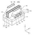
도 1은 예시적인 실시예들에 따른 반도체 장치를 도시하는 사시도이다. 도 2a 내지 도 2c는 도 1의 반도체 장치를 각각 절단선 A-A', B-B' 및 C-C'를 따라서 절단한 단면도이다. 설명의 편의를 위하여, 도 1에서는 주요 구성요소만을 도시하였으며, 예를 들어, 도 2a 내지 도 2c의 층간 절연층(160)을 생략하고 도시하였다.1 is a perspective view showing a semiconductor device according to exemplary embodiments; 2A to 2C are cross-sectional views of the semiconductor device of FIG. 1 cut along the cutting lines A-A ', B-B', and C-C ', respectively. For convenience of explanation, only the main components are shown in FIG. 1, and for example, the
도 1 내지 도 2c를 참조하면, 반도체 장치(100)는, 기판(101), 활성 핀들(105), 소스/드레인 영역들(110), 게이트 구조물(140) 및 콘택 플러그들(180)을 포함할 수 있다. 반도체 장치(100)는, 소자 분리층들(107), 스페이서(150) 및 층간 절연층(160)을 더 포함할 수 있다.1 to 2C, a
본 실시예의 반도체 장치(100)는 활성 핀들(105)이 핀(fin) 구조를 갖는 트랜지스터인 핀펫(FinFET)일 수 있다.
The
기판(101)은 x 방향과 y 방향으로 연장되는 상면을 가질 수 있다. 기판(101)은 반도체 물질, 예컨대 Ⅳ족 반도체, Ⅲ-Ⅴ족 화합물 반도체 또는 Ⅱ-Ⅵ족 산화물 반도체를 포함할 수 있다. 예를 들어, Ⅳ족 반도체는 실리콘, 게르마늄 또는 실리콘-게르마늄을 포함할 수 있다. 기판(101)은 벌크 웨이퍼, 에피택셜층, 에피택셜 층, SOI(Silicon On Insulator)층, 또는 SeOI(Semiconductor On Insulator)층 등으로 제공될 수도 있다.The
소자 분리층들(107)은 기판(101)에서 활성 핀들(105)을 정의할 수 있다. 소자 분리층들(107)은 절연 물질로 이루어질 수 있다. 소자 분리층들(107)은 예를 들어, 쉘로우 트랜치 소자 분리(shallow trench isolation, STI) 공정에 의하여 형성될 수 있다. 소자 분리층들(107)은 예를 들어, 산화물, 질화물 또는 그들의 조합일 수 있다.The device isolation layers 107 may define the
활성 핀들(105)은 기판(101) 내에서 소자 분리층들(107)에 의해 정의되며, 제1 방향, 예를 들어 y 방향으로 연장되도록 배치될 수 있다. 활성 핀들(105)은 기판(101)으로부터 돌출된 활성 핀(fin)의 구조를 가질 수 있다. 활성 핀들(105)은 기판(101)의 일부로 이루어질 수도 있고, 기판(101)으로부터 성장된 에피택셜층을 포함할 수도 있다. 다만, 게이트 구조물(140)의 측면에서는 기판(101) 상의 활성 핀들(105)이 리세스되고 소스/드레인 영역들(110)이 배치될 수 있다.
The
소스/드레인 영역들(110)은 게이트 구조물(140)의 양측에서, 활성 핀들(105) 상에 배치될 수 있다. 소스/드레인 영역들(110)은 반도체 장치(100)의 소스 영역 또는 드레인 영역으로 제공될 수 있다. 소스/드레인 영역들(110)은 상면이 게이트 구조물(140)의 하면보다 높게 위치하는 엘리베이티드(elevated) 소스/드레인 형태일 수 있다. 본 실시예에서, 소스/드레인 영역들(110)은 오각형 형상으로 도시되었으나, 소스/드레인 영역들(110)은 다양한 형상을 가질 수 있으며, 예를 들어, 다각형, 원형 및 직사각형 중 어느 하나의 형상을 가질 수 있다. 소스/드레인 영역들(110)은 세 개의 활성 핀들(105) 상에서 서로 연결된 또는 합쳐진(merged) 구조를 가질 수 있다. 다만, 연결되는 활성 핀들(105)의 개수는 도시된 것에 한정되지 않는다.The source /
소스/드레인 영역들(110)은 예를 들어, 실리콘 또는 실리콘 게르마늄(SiGe)을 포함할 수 있다. 특히, 소스/드레인 영역들(110)은 에피택셜층으로 이루어질 수 있다. 예를 들어, 소스/드레인 영역들(110)이 실리콘 게르마늄(SiGe)을 포함하는 경우, 실리콘(Si)으로 이루어진 활성 핀(105)의 일 영역인 반도체 장치(100)의 채널 영역에 응력을 가하여 정공의 이동도(mobility)를 향상시킬 수 있다.
The source /
소스/드레인 영역들(110)은 서로 다른 농도의 원소를 포함하는 제1 내지 제3 영역(112, 114, 116)을 포함할 수 있다.The source /
제1 영역들(112)은 활성 핀들(105) 상에 배치될 수 있다. 제2 영역들(114)은 제1 영역들(112)으로부터 성장되고, 활성 핀들(105) 상에서 서로 연결될 수 있다.The
제2 영역(114)은 제1 영역(112)과 함께 오각형의 형상을 이룰 수 있다. 제2 영역들(114)은 기판(101)의 상면에 대하여 경사진 표면들(114S)을 가질 수 있다. 제2 영역들(114)의 표면들(114S)은 결정학 면에 해당할 수 있으며, 예를 들어, 제2 영역들(114)이 실리콘 게르마늄(SiGe)으로 이루어진 경우, (111) 면 또는 이의 등가 면일 수 있다.The
제3 영역(116)은 제2 영역들(114)의 상부에서 제2 영역들(114) 사이에 배치되어, 연결 영역 또는 브릿지 영역을 형성할 수 있다. 구체적으로, 제3 영역(116)은 인접하는 제2 영역들(114)의 사이에서 제2 영역(114)의 경사진 표면(114S) 상에 배치될 수 있다. 제3 영역(116)의 상면은 하부로 오목한 형태의 굴곡을 가질 수 있으나, 이에 한정되지 않는다. 예를 들어, 다른 실시예에서, 제3 영역(116)의 상면은 기판(101)의 상면에 평행한 평탄한 면일 수 있다.
The
제1 내지 제3 영역(112, 114, 116)은 서로 다른 농도의 원소 및/또는 도핑 원소를 포함하는 영역들일 수 있다.The first to
예를 들어, 제1 영역(112)은 제1 농도의 게르마늄(Ge)을 포함하고, 제2 영역(114)은 상기 제1 농도보다 높은 제2 농도의 게르마늄(Ge)을 포함하며, 제3 영역(116)은 상기 제2 농도보다 높은 제3 농도의 게르마늄(Ge)을 포함할 수 있다. 상기 제1 농도는 30 at. %(atomic percentage) 이하일 수 있으며, 상기 제2 농도는 20 at. % 내지 60 at. %의 범위를 가질 수 있으며, 상기 제3 농도는 50 at. % 내지 80 at. %의 범위를 가질 수 있으나, 이에 한정되지는 않는다.For example, the
제1 내지 제3 영역(112, 114, 116)은 서로 다른 농도의 도핑 원소를 포함할 수도 있다. 예를 들어, 제1 영역(112)은 제1 농도의 붕소(B)를 포함하고, 제2 영역(114)은 상기 제1 농도보다 높은 제2 농도의 붕소(B)를 포함하며, 제3 영역(116)은 상기 제2 농도보다 높은 제3 농도의 붕소(B)를 포함할 수 있다. 제1 내지 제3 영역(112, 114, 116)은 게르마늄(Ge)의 농도가 상이하면서 동시에 도핑 원소의 농도가 상이하거나, 어느 하나만 상이할 수 있다.
The first to
게이트 구조물(140)은 활성 핀들(105)의 상부에서 활성 핀들(105)과 교차하도록 배치되며, 게이트 절연층(142) 및 제1 및 제2 게이트 전극(145, 147)을 포함할 수 있다.The
게이트 절연층(142)은 활성 핀들(105)과 제1 및 제2 게이트 전극(145, 147)의 사이에 배치될 수 있다. 게이트 절연층(142)은 산화물, 질화물 또는 고유전율(high-k) 물질을 포함할 수 있다. 상기 고유전율 물질은, 실리콘 산화막(SiO2)보다 높은 유전 상수(dielectric constant)를 가지는 유전 물질을 의미할 수 있다. 상기 고유전율 물질은, 예를 들어, 알루미늄 산화물(Al2O3), 탄탈륨 산화물(Ta2O3), 티타늄 산화물(TiO2), 이트륨 산화물(Y2O3), 지르코늄 산화물(ZrO2), 지르코늄 실리콘 산화물(ZrSixOy), 하프늄 산화물(HfO2), 하프늄 실리콘 산화물(HfSixOy), 란탄 산화물(La2O3), 란탄 알루미늄 산화물(LaAlxOy), 란탄 하프늄 산화물(LaHfxOy), 하프늄 알루미늄 산화물(HfAlxOy), 및 프라세오디뮴 산화물(Pr2O3) 중 어느 하나일 수 있다. 다른 실시예에서, 게이트 절연층(142)은 제1 및 제2 게이트 전극(145, 147)의 하면에만 형성될 수도 있다.A
제1 및 제2 게이트 전극(145, 147)은 순차적으로 게이트 절연층(142) 상에 배치될 수 있다. 반도체 장치(100)가 트랜지스터인 경우, 제1 및 제2 게이트 전극(145, 147)과 교차되는 활성 핀들(105)에는 채널 영역이 형성될 수 있다. 제1 및 제2 게이트 전극(145, 147)은 서로 다른 물질로 이루어질 수 있다. 제1 게이트 전극(145)은 예를 들어, 티타늄 질화막(TiN), 탄탈륨 질화막(TaN), 또는 텅스텐 질화막(WN)과 같은 금속 질화물을 포함할 수 있다. 제2 게이트 전극(147)은 예를 들어, 알루미늄(Al), 텅스텐(W), 또는 몰리브덴(Mo) 등의 금속 물질 또는 도핑된(doped) 폴리실리콘과 같은 반도체 물질을 포함할 수 있다. 제1 게이트 전극(145)은 제2 게이트 전극(147)에 대한 확산 방지층으로서의 역할을 할 수 있으나, 이에 한정되지는 않는다. 다른 실시예에서, 게이트 전극은 하나의 층으로 이루어질 수도 있다.The first and
스페이서(150)는 게이트 구조물(140)의 양 측면에 배치될 수 있다. 스페이서(150)는 소스/드레인 영역들(110)과 제1 및 제2 게이트 전극(145, 147)을 절연시킬 수 있다. 스페이서(150)는 산화물, 질화물 및 산질화물로 이루어질 수 있으며, 다층막으로 이루어질 수도 있다. 예를 들어, 스페이서(150)는 실리콘 질화막 및 저유전율(low-k)막의 적층 구조를 가질 수 있다.
The
콘택 플러그들(180)은 소스/드레인 영역들(110) 상에 배치되며, 소스/드레인 영역들(110)에 신호가 인가되도록 반도체 장치(100)의 다른 구성 요소에 전기적으로 연결할 수 있다. 콘택 플러그들(180)은 평면 상에서 세장형(elongated)의 형상을 가질 수 있다. 즉, 콘택 플러그들(180)은 게이트 구조물(140)의 연장 방향, 즉 x 방향을 따라 연장된 형상을 가질 수 있으며, 직사각형 또는 타원형 등의 형상을 가질 수 있다.The contact plugs 180 are disposed on the source /
콘택 플러그들(180)은 제1 및 제2 층간 절연층(162, 164)을 관통하여 소스/드레인 영역들(110)과 연결될 수 있다. 콘택 플러그들(180)은 소스/드레인 영역(110)의 일부를 제1 깊이(D1) 내지 제2 깊이(D2)로 리세스하도록 배치되어 소스/드레인 영역(110)과 연결될 수 있다. 콘택 플러그들(180)이 소스/드레인 영역(110)을 리세스하는 깊이는 영역에 따라 상이할 수 있으며, 예를 들어, x 방향을 따라 서로 상이할 수 있다. 제1 및 제2 깊이(D1, D2)는 도시된 것에 한정되지 않으며, 소스/드레인 영역(110)과 콘택 플러그(180)가 안정적으로 접속되고, 콘택 플러그(180)의 하면이 굴곡을 가지도록 형성될 수 있는 범위에서 선택될 수 있다.The contact plugs 180 may be connected to the source /
콘택 플러그들(180)의 하면은 도 2a에 도시된 것과 같이, 소스/드레인 영역(110)의 제2 및 제3 영역(114, 116)의 경계를 따라 굴곡을 가질 수 있다. 즉, 콘택 플러그들(180)은 웨이브(wavy) 하면을 가질 수 있다. 콘택 플러그들(180)의 하면은 제2 영역(114)의 중심에서 기판(101)의 상면으로부터 제1 높이(H1)에 위치하고, 제3 영역(116)의 중심에서 제1 높이(H1)보다 낮은 제2 높이(H2)에 위치할 수 있다. 이러한 콘택 플러그들(180)의 하면의 형상은 콘택 플러그(180)의 형성을 위한 콘택 홀 형성 시, 제2 영역(114)과 제3 영역(116)의 식각률의 차이에 의한 것일 수 있다. 이에 대해서는 하기에 도 17a 내지 도 17c를 참조하여 더욱 상세히 설명한다.The bottom surface of the contact plugs 180 may have a curvature along the boundaries of the second and
콘택 플러그들(180)은 이와 같은 굴곡진 하면을 가지므로, 소스/드레인 영역(110)과의 접촉 면적이 증가될 수 있다. 또한, 본 실시예에서는 콘택 플러그들(180)이 제3 영역(116)과 연결되므로, 제3 영역(116)이 게르마늄(Ge) 고농도 영역인 경우, 상대적으로 쇼트키(Schottky) 베리어 높이가 낮아져서 접촉 저항이 감소될 수 있다. 예를 들어, 제3 영역(116)이 붕소(B) 고농도 영역인 경우, 쇼트키 베리어 폭에 영향을 주어 접촉 저항이 감소될 수 있다.Since the contact plugs 180 have such a curved bottom surface, the contact area with the source /
시뮬레이션 결과에 따르면, 콘택 플러그(180)의 하면이 평탄한 비교예의 경우 반도체 장치의 전류량이 목표값의 약 63 %이었다. 하지만, 동일한 조건에서 본 실시예들과 같이 콘택 플러그(180)의 하면에 굴곡이 있는 경우, 소스/드레인 영역(110)의 리세스된 깊이에 따라 반도체 장치(100)의 전류량이 목표값의 약 83 내지 89 %의 범위로 나타났다. 이러한 결과로부터, 콘택 플러그(180)의 하면에 굴곡이 있는 경우 반도체 장치(100)의 전기적 특성이 향상됨을 알 수 있다.According to the simulation results, in the case of the flat comparative example of the lower surface of the
콘택 플러그들(180)은 실리사이드층(182)과 제1 및 제2 도전층(184, 186)을 포함할 수 있다. 실리사이드층(182)은 소스/드레인 영역(110)과 접촉되도록 배치될 수 있다. 실리사이드층(182)은 제1 도전층(184)의 일부가 소스/드레인 영역(110)에 의해 실리사이드화되어 형성된 층일 수 있으며, 실시예에 따라 생략될 수도 있다. 실리사이드층(182)은 예를 들어, 티타늄실리사이드일 수 있다. 제1 도전층(184)은 제2 도전층(186)을 이루는 금속 물질에 대한 확산 방지층으로 기능할 수 있다. 제1 도전층(184)은 소스/드레인 영역들(110)의 상부 및 콘택 플러그들(180)의 측벽을 따라 형성될 수 있다. 제1 도전층(184)은 예를 들어, 티타늄 질화막(TiN), 탄탈륨 질화막(TaN), 또는 텅스텐 질화막(WN) 등 중의 적어도 하나의 금속 질화물을 포함할 수 있다. 제2 도전층(186)은 알루미늄(Al), 구리(Cu), 텅스텐(W), 몰리브데늄(Mo) 등과 같은 도전성 물질을 포함할 수 있다.
The contact plugs 180 may include a
층간 절연층(160)은 제1 및 제2 층간 절연층(162, 164)을 포함할 수 있으며, 기판(101), 소스/드레인 영역들(110) 및 게이트 구조물(140)을 덮도록 배치될 수 있다. 제1 층간 절연층(162)의 높이는 게이트 구조물(140)의 높이와 실질적으로 동일할 수 있다. 다만, 제1 및 제2 층간 절연층(162, 164)은 공정 상에서 구별되는 층들로, 상대적인 높이 및 경계면의 위치는 도면에 도시된 것에 한정되지 않는다. 다른 실시예에서, 제1 및 제2 층간 절연층(162, 164)은 하나의 층으로 이루어질 수도 있다. 제1 및 제2 층간 절연층(162, 164)은 절연성 물질로 이루어질 수 있으며, 산화막, 질화막 및 산질화막 중 적어도 하나를 포함할 수 있다. 예를 들어, 제1 층간 절연층(162)은 TOZ(tonen silazene)막이고, 제2 층간 절연층(164)은 TEOS(tetraethylortho silicate)막일 수 있다.
The interlayer insulating
도 3 내지 도 6은 예시적인 실시예들에 따른 반도체 장치를 도시하는 도면들이다.FIGS. 3 to 6 are views showing a semiconductor device according to exemplary embodiments. FIG.
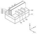
도 3의 사시도를 참조하면, 반도체 장치(100a)는 기판(101), 활성 핀들(105), 소스/드레인 영역들(110a), 게이트 구조물(140) 및 콘택 플러그들(180)을 포함할 수 있다. 반도체 장치(100a)는, 소자 분리층들(107) 및 스페이서(150)를 더 포함할 수 있다.3, the
소스/드레인 영역들(110a)은 제1 내지 제3 영역(112, 114, 116a)을 포함할 수 있다. 본 실시예의 반도체 장치(100a)는 도 1의 반도체 장치(100)와 달리, 제3 영역(116a)이 제2 영역들(114) 사이에서 제2 영역들(114)의 경사진 표면(114S)의 일부를 노출시키고 일부 상에만 배치될 수 있다. 즉, 제3 영역(116a)의 두께가 상대적으로 작을 수 있으며, 제3 영역(116a)의 두께는 실시예들에서 다양하게 변경될 수 있다. 이에 따라, 콘택 플러그(180)의 하면의 형상도 도 1의 실시예에서와 다르게 형성될 수 있을 것이다.
The source /
도 4a 및 도 4b를 참조하면, 각각 도 2a 및 도 2c에 대응되는 영역의 단면들을 도시한다. 반도체 장치(100b)는 기판(101), 활성 핀들(105), 소스/드레인 영역들(110), 게이트 구조물(140) 및 콘택 플러그들(180a)을 포함할 수 있다. 반도체 장치(100b)는, 소자 분리층들(107) 및 스페이서(150)를 더 포함할 수 있다.Referring to Figures 4A and 4B, there are shown cross-sections of regions corresponding to Figures 2A and 2C, respectively. The
본 실시예에서 콘택 플러그들(180a)은 소스/드레인 영역(110)의 제3 영역(116)을 모두 리세스하고 제2 영역(114)과 연결될 수 있다. 즉, 콘택 플러그들(180a)이 소스/드레인 영역(110)을 리세스하는 깊이 및 이에 따른 콘택 플러그들(180a)의 하면의 위치는 실시예들에서 다양하게 변경될 수 있다.In this embodiment, the contact plugs 180a may be recessed in all of the
콘택 플러그들(180a)의 하면의 높이는 제2 영역(114)의 일 단에서의 높이(H3)보다 제3 영역(116)이 리세스된 영역에서의 높이(H4)가 더 낮을 수 있다. 즉, 콘택 플러그(180a)는 제3 영역(116) 또는 제3 영역(116)이 리세스된 영역에서 기판(101)을 기준으로 가장 낮은 높이에 위치할 수 있다.
The height of the lower surface of the contact plugs 180a may be lower than the height H3 at one end of the
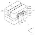
도 5a 및 도 5b를 참조하면, 도 5b는 도 5a의 사시도에서 절단선 D-D'를 따른 단면을 도시한다. 반도체 장치(100c)는 기판(101), 활성 핀들(105), 소스/드레인 영역들(110b), 게이트 구조물(140) 및 콘택 플러그들(180)을 포함할 수 있다. 반도체 장치(100c)는, 소자 분리층들(107) 및 스페이서(150)를 더 포함할 수 있다.Referring to FIGS. 5A and 5B, FIG. 5B shows a cross section taken along the section line D-D 'in the perspective view of FIG. 5A. The
소스/드레인 영역들(110b)은 두 개의 활성 핀들(105) 상에서 연결되도록 배치될 수 있다. 또한, 소스/드레인 영역들(110b)은 제1 내지 제3 영역(112, 114, 116) 외에 제4 영역(113)을 더 포함할 수 있다. 제4 영역(113)은 제1 및 제2 영역(112, 114)의 사이에 배치될 수 있으며, 원형 또는 타원형에 가까운 형상으로 도시되었으나 이에 한정되지 않는다. 제4 영역(113)은 제1 및 제2 영역(112, 114)과 다른 농도의 원소 및/또는 도핑 원소를 포함하는 영역일 수 있다.The source /
예를 들어, 제1 영역(112)은 제1 농도의 게르마늄(Ge)을 포함하고, 제4 영역(113)은 상기 제1 농도보다 높은 제2 농도의 게르마늄(Ge)을 포함하며, 제2 영역(114)은 상기 제2 농도보다 높은 제3 농도의 게르마늄(Ge)을 포함할 수 있다. 또한, 제3 영역(116)은 상기 제3 농도보다 높은 제4 농도의 게르마늄(Ge)을 포함할 수 있다.For example, the
다른 실시예들에서, 소스/드레인 영역들(110b)은 목적하는 콘택 플러그(180)의 콘택 저항 특성, 반도체 장치(100b)의 채널 영역에 인가되는 응력 등을 고려하여, 제4 영역(113) 이외에도 서로 다른 농도의 원소를 포함하는 복수의 영역들을 더 포함할 수 있다.
In other embodiments, the source /
도 6의 사시도를 참조하면, 반도체 장치(100d)는 기판(101), 활성 핀들(105), 소스/드레인 영역들(110c), 게이트 구조물(140) 및 콘택 플러그들(180)을 포함할 수 있다. 반도체 장치(100d)는, 소자 분리층들(107) 및 스페이서(150)를 더 포함할 수 있다.6, the
소스/드레인 영역들(110c)은 제1 내지 제3 영역(112, 114, 116) 외에 제5 영역(118)을 더 포함할 수 있다. 제5 영역(118)은 제2 및 제3 영역(114, 116)의 외표면을 둘러싸도록 배치될 수 있으며, 두께는 도시된 두께에 한정되지 않는다. 본 실시예에서, 제5 영역(118)은 제2 영역(114)의 하면 중 인접한 제2 영역들(114) 사이의 면들 상에는 배치되지 않는 것으로 도시되었으나, 이에 한정되지는 않는다. 제5 영역(118)은 제1 내지 제3 영역(112, 114, 116)과 다른 농도의 원소 및/또는 도핑 원소를 포함하는 영역일 수 있다.The source /
제5 영역(118)은 후속 공정 중에 제3 영역(116)을 보호할 수 있다. 예를 들어, 제5 영역(118)은 실리콘(Si) 캡핑층일 수 있다. 예를 들어, 제3 영역(116)이 상대적으로 녹는점이 낮은 실리콘 게르마늄(SiGe)으로 이루어진 경우, 게르마늄(Ge)을 거의 포함하지 않는 실리콘(Si)으로 제5 영역(118)을 형성함으로써, 후속 공정 중에 제3 영역(116)을 보호할 수 있다.
The
도 7 내지 도 18은 예시적인 실시예들에 따른 반도체 장치의 제조 방법을 설명하기 위하여 공정 순서에 따라 도시한 도면들이다.FIGS. 7 to 18 are views showing a process sequence in order to explain a method of manufacturing a semiconductor device according to exemplary embodiments. FIG.
도 7을 참조하면, 기판(100)을 패터닝하여 활성 핀(105)을 정의하는 트렌치(TI)를 형성할 수 있다.Referring to FIG. 7, a substrate (100) may be patterned to form a trench (TI) defining active pin (105).
먼저, 기판(100) 상에 패드 산화물 패턴(122) 및 마스크 패턴(124)을 형성할 수 있다. 패드 산화물 패턴(122)은 활성 핀(105)의 상면을 보호하기 위한 층일 수 있으며, 실시예에 따라 생략될 수도 있다. 마스크 패턴(124)은 기판(100)을 패터닝하기 위한 마스크층으로, 실리콘 질화물, 탄소 함유물 등을 포함할 수 있다. 마스크 패턴(124)은 다층 구조로 이루어질 수도 있다.First, a pad oxide pattern 122 and a mask pattern 124 may be formed on the
패드 산화물 패턴(122) 및 마스크 패턴(124)을 이용하여 기판(100)을 이방성 식각하여 트렌치(TI)를 형성할 수 있다. 트렌치(TI)는 높은 종횡비를 가지므로, 하부로 갈수록 폭이 좁아질 수 있으며, 이에 따라 활성 핀(105)은 상부로 갈수록 좁아지는 형상을 가질 수 있다.
The
도 8을 참조하면, 트렌치(TI)를 매립하는 소자 분리층(107)을 형성할 수 있다.Referring to FIG. 8, the
먼저, 트렌치(TI)를 절연성 물질로 매립한 후 평탄화하는 공정이 수행될 수 있다. 평탄화 공정 중에 패드 산화물 패턴(122) 및 마스크 패턴(124)의 적어도 일부가 제거될 수 있다. 다른 실시예에서, 트렌치(TI) 내에 상대적으로 얇은 라이너층을 먼저 형성한 후 트렌치(TI)를 매립할 수도 있다.First, a process of filling the trench TI with an insulating material and then planarizing the trench TI may be performed. During the planarization process, at least a portion of the pad oxide pattern 122 and the mask pattern 124 may be removed. In another embodiment, a relatively thin liner layer may be first formed in the trench TI and then the trench TI may be buried.
다음으로, 트렌치(TI)를 매립한 상기 절연성 물질을 일부 제거함으로써 활성 핀(105)이 기판(101) 상으로 돌출되도록 하는 공정이 수행될 수 있다. 이러한 공정은, 예를 들어, 패드 산화물 패턴(122)의 적어도 일부를 식각 마스크로 이용하는 습식 식각 공정으로 수행될 수 있다. 이에 의해, 활성 핀(105)이 상부로 소정 높이(H5)만큼 돌출될 수 있으며, 돌출되는 높이(H5)는 다양하게 변화될 수 있다. 식각 중에, 패드 산화물 패턴(122)도 함께 제거될 수 있다.
Next, a process of causing the
도 9를 참조하면, 활성 핀들(105)과 교차하여 연장되는 더미 게이트 절연층(132), 더미 게이트 전극(135) 및 스페이서(150)를 형성할 수 있다.Referring to FIG. 9, a dummy
더미 게이트 절연층(132) 및 더미 게이트 전극(135)은 예를 들어, 마스크 패턴층(136)을 이용하여 식각 공정을 수행함으로써 형성할 수 있다.The dummy
더미 게이트 절연층(132) 및 더미 게이트 전극(135)은 게이트 절연층(142) 및 제1 및 제2 게이트 전극(145, 147)(도 1 참조)이 형성될 영역에 형성되며, 후속 공정 중에 제거될 수 있다. 예를 들어, 더미 게이트 절연층(132)은 실리콘 산화물을 포함할 수 있으며, 더미 게이트 전극(135)은 폴리 실리콘을 포함할 수 있다.The dummy
스페이서(150)는 더미 게이트 절연층(132), 더미 게이트 전극(135) 및 마스크 패턴층(136)의 상부에 균일한 두께의 막을 형성한 후 이를 이방성 식각하여 형성할 수 있다. 스페이서(150)는 복수의 막을 적층한 구조를 가질 수도 있다.
The
도 10을 참조하면, 스페이서(150)의 양측에서 활성 핀(105)을 선택적으로 제거할 수 있다.Referring to FIG. 10,
스페이서(150)의 양측에서 활성 핀(105)을 제거함으로써 리세스가 형성될 수 있다. 상기 리세스는 별도의 마스크층을 형성하거나, 마스크 패턴층(136) 및 스페이서(150)를 마스크로 이용하여 활성 핀(105)의 일부를 식각함으로써 형성할 수 있다. 상기 리세스는 예를 들어, 건식 식각 공정과 습식 식각 공정을 순차적으로 적용하여 형성할 수 있다. 선택적으로, 상기 리세스의 형성 후, 별도의 공정을 통해 리세스된 활성 핀(105)의 표면을 큐어링하는 공정이 수행될 수도 있다. 본 실시예에서, 리세스된 활성 핀(105)의 상면은 소자 분리층(107)의 상면과 동일한 레벨인 것으로 도시되었으나, 이에 한정되지 않는다. 다른 실시예에서, 리세스된 활성 핀(105)의 상면은 소자 분리층(107)의 상면보다 높거나 낮을 수 있다.A recess can be formed by removing the
상기 리세스의 형성 전 또는 형성 후에, 더미 게이트 전극(135) 양측의 활성 핀(105)에 불순물을 주입하는 공정이 수행될 수 있다. 불순물 주입 공정은 마스크 패턴층(136) 및 스페이서(150)를 마스크로 이용하여 수행될 수 있다.
A process of implanting impurities into
도 11을 참조하면, 스페이서(150) 양측의 리세스된 활성 핀(105) 상에 소스/드레인 영역(110)의 제1 영역(112)을 형성할 수 있다.Referring to FIG. 11, a
이하에서, 도 10 내지 도 12를 참조하여 설명하는 소스/드레인 영역(110)의 형성 공정은, 예를 들어 선택적 에피택셜 성장(Selective Epitaxial Growth, SEG) 공정을 이용할 수 있다.Hereinafter, the forming process of the source /
소스/드레인 영역(110)은 예를 들어, 실리콘 게르마늄(SiGe)층일 수 있다. 실리콘(Si)으로 이루어진 활성 핀(105) 상에 실리콘 게르마늄(SiGe)이 성장되는 경우, 반도체 장치의 채널 영역에 압축 응력을 발생시킬 수 있다. 이 경우, 활성 핀(105)과의 격자 상수 차이에 의한 결함 발생을 감소시키기 위한 버퍼층으로서, 상대적으로 낮은 제1 농도의 게르마늄(Ge)을 포함하는 제1 영역(112)을 형성할 수 있다.The source /
소스/드레인 영역(110)의 성장 중에 붕소(B)와 같은 불순물이 인-시추(in-situ)로 도핑되거나, 성장 후에 별도로 주입될 수 있다.
During growth of the source /
도 12를 참조하면, 소스/드레인 영역(110)의 제1 영역(112) 상에 제2 영역(114)을 형성할 수 있다.Referring to FIG. 12, a
제2 영역(114)은 각각의 활성 핀(105) 상에 성장된 영역들(114A, 114B)을 포함할 수 있으며, 이들은 성장 과정에서 서로 연결되어 연결부(ME)를 형성할 수 있다. 각각의 활성 핀(105) 상에 성장된 영역들(114A, 114B)은 서로 동일하거나 다른 농도의 게르마늄(Ge)을 포함할 수 있다. 제2 영역(114)은 성장 과정에서 결정학적으로 안정적인 면을 따라 성장되어 도시된 것과 같은 오각형 또는 육각형의 형상을 가질 수 있다. 따라서, 제2 영역(114)의 표면(114S)은 기판(101)에 대하여 경사진 각도를 가질 수 있다. 이와 같이 표면(114S)이 결정학적으로 안정된 면으로 성장되는 경우, 일정 크기로 성장된 후에는 성장 시간이 증가하여도 성장이 거의 일어나지 않을 수 있다.The
제2 영역(114)은 제1 영역(112)의 상기 제1 농도보다 높은 제2 농도의 게르마늄(Ge)을 포함할 수 있다. 또한, 제2 영역(114)은 제1 영역(112)보다 높은 농도의 붕소(B)와 같은 도핑 원소를 포함할 수 있으나, 이에 한정되지는 않는다.
The
도 13을 참조하면, 소스/드레인 영역(110)의 제2 영역(114) 상에 제3 영역(116)을 형성할 수 있다.Referring to FIG. 13, a
제3 영역(116)은 서로 인접한 제2 영역들(114)의 사이, 예를 들어 도 12의 연결부(ME) 상에 성장될 수 있다. 구체적으로, 서로 'V'자 형상으로 마주하는 제2 영역(114)의 표면들(114S) 상에 성장될 수 있다. 제3 영역(116)은 성장 온도, 게르마늄(Ge) 소스량과 같은 공정 조건을 조절함으로써, 제2 영역(114)의 단부에서의 표면(114S)에서 성장되지 않고, 'V'자 형상으로 마주하는 표면들(114S) 상에서만 성장되도록 제어될 수 있다. 예를 들어, 제3 영역(116)은 제2 영역(114)의 성장 시보다 낮은 온도 및/또는 많은 게르마늄(Ge) 소스량의 조건에서 성장될 수 있다.The
제3 영역(116)은 제2 영역(114)의 상기 제2 농도보다 높은 제3 농도의 게르마늄(Ge)을 포함할 수 있다. 또한, 제3 영역(116)은 제2 영역(114)보다 높은 농도의 붕소(B)와 같은 도핑 원소를 포함할 수 있으나, 이에 한정되지는 않는다.The
본 단계에 의해, 제1 내지 제3 영역(112, 114, 116)을 포함하는 소스/드레인 영역(110)이 형성될 수 있다.
By this step, the source /
도 14를 참조하면, 소스/드레인 영역(110) 상에 제1 층간 절연층(162)을 형성할 수 있다.Referring to FIG. 14, a first
제1 층간 절연층(162)은 절연성 물질로 마스크 패턴층(136), 스페이서(150) 및 소스/드레인 영역(110)을 덮는 층을 형성한 후, 평탄화 공정을 통해 더미 게이트 전극(135)의 상면이 노출되도록 함으로써 형성될 수 있다. 따라서, 본 단계에서 마스크 패턴층(136)이 제거될 수 있다.The first
제1 층간 절연층(162)은, 예를 들어, 산화물, 질화물 ?? 산질화물 중 적어도 하나를 포함할 수 있다.
The first
도 15를 참조하면, 더미 게이트 절연층(132) 및 더미 게이트 전극(135)을 제거할 수 있다.Referring to FIG. 15, the dummy
더미 게이트 절연층(132) 및 더미 게이트 전극(135)은 하부의 소자 분리층(107) 및 활성 핀들(105)에 대하여 선택적으로 제거되어, 소자 분리층(107) 및 활성 핀들(105)을 노출시키는 개구부(E)가 형성될 수 있다.The dummy
더미 게이트 절연층(132) 및 더미 게이트 전극(135)의 제거 공정은, 건식 식각 공정 및 습식 식각 공정 중 적어도 하나를 이용할 수 있다.
The dummy
도 16을 참조하면, 개구부(E) 내에 게이트 절연층(142) 및 제1 및 제2 게이트 전극(145, 147)을 형성하여 게이트 구조물(140)을 형성할 수 있다.Referring to FIG. 16, a
게이트 절연층(142)은 개구부(E)의 측벽 및 하면을 따라 실질적으로 컨포멀하게 형성될 수 있다. 게이트 절연층(142)은 게이트 절연층(142)은 산화물, 질화물 또는 고유전율(high-k) 물질을 포함할 수 있다.The
제1 및 제2 게이트 전극(145, 147)은 금속 또는 반도체 물질을 포함할 수 있다.
The first and
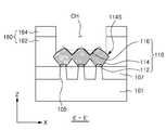
도 17a 내지 도 17c를 참조하면, 도 17b 및 도 17c는 각각 도 17a의 사시도의 절단선 E-E' 및 F-F'를 따라서 절단한 단면들을 도시한다.17A to 17C, Figs. 17B and 17C show cross sections taken along the cutting lines E-E 'and F-F', respectively, in the perspective view of Fig. 17A.
본 단계에서는, 층간 절연층(162, 164)을 패터닝하여 콘택 홀(OP)을 형성할 수 있다.In this step, the contact holes OP can be formed by patterning the
포토레지스트 패턴과 같은 별도의 마스크층을 이용하여, 콘택 플러그(180)(도 1 참조)가 형성될 영역에서 층간 절연층(162, 164)을 제거함으로써, 콘택 홀(OP)을 형성할 수 있다. 층간 절연층(162, 164)의 제거 시, 소스/드레인 영역(110)의 상부가 일부 함께 제거되어 리세스될 수 있다. 따라서, 콘택 홀(OP)을 통해 소스/드레인 영역(110)의 리세스된 상면의 적어도 일부가 노출될 수 있다. 콘택 홀(OP)의 하면은 도시된 것과 같이, 소스/드레인 영역(110)의 리세스된 상면을 따라 굴곡을 가질 수 있다.The contact hole OP can be formed by removing the
소스/드레인 영역(110)의 제2 영역(114)과 제3 영역(116)은 적어도 일 원소, 예를 들어, 게르마늄(Ge)의 농도가 서로 다를 수 있으며, 이에 따라 식각률이 다를 수 있다. 제3 영역(116)의 게르마늄(Ge)의 농도가 제2 영역(114)보다 높은 경우, 콘택 홀(OP)의 형성 시, 제3 영역(116)의 식각률이 제2 영역(114)보다 높게 제어될 수 있다. 따라서, 콘택 홀(OP)의 하면은 제2 영역(114)과 제3 영역(116)의 경계에 대응되는 굴곡을 가질 수 있다. 즉, 제3 영역(116)이 제2 영역(114)보다 상대적으로 많이 제거되어 굴곡이 형성될 수 있다. 다만, 제2 및 제3 영역(114, 116)의 리세스된 깊이 및 프로파일은 도시된 것에 한정되지 않으며, 공정 조건에 따라 변화될 수 있다.The
이와 같이 콘택 홀(OP)이 굴곡진 하면을 가지므로, 후속에서 콘택 홀(OP) 내에 형성되는 콘택 플러그들(180)(도 18 참조)는 소스/드레인 영역(110)과의 접촉 면적이 증가될 수 있다. 또한, 콘택 플러그들(180)이 제3 영역(116)과 연결되는 경우, 제3 영역(116)이 게르마늄(Ge) 고농도 영역이므로 상대적으로 쇼트키 베리어 높이가 낮아져서 접촉 저항이 감소될 수 있다. 또한, 제3 영역(116)이 붕소(B) 고농도 영역인 경우, 쇼트키 베리어 폭에 영향을 주어 접촉 저항이 감소될 수 있다.
The contact plugs 180 (see FIG. 18) formed in the contact holes OP in the subsequent process are formed in such a manner that the contact areas with the source /
도 18을 참조하면, 콘택 홀(OP) 내에 도전성 물질을 매립하여 콘택 플러그들(180)을 형성할 수 있다.Referring to FIG. 18, a conductive material may be embedded in the contact hole OP to form the contact plugs 180.
제1 및 제2 도전층(184, 186)이 순차적으로 증착되어 콘택 홀(OP)이 매립될 수 있다. 소스/드레인 영역(110)과의 계면에 형성되는 실리사이드층(182)(도 2a 참조)은 본 단계 또는 후속의 단계에서, 제1 도전층(184) 물질과 소스/드레인 영역(110) 물질이 반응하여 형성될 수 있다.
The first and second
도 19는 예시적인 실시예들에 따른 반도체 장치의 일부를 나타내는 전자 현미경 사진이다.19 is an electron micrograph showing a part of the semiconductor device according to the exemplary embodiments.
도 19를 참조하면, 투과 전자 현미경(Transmission Electron Microscope, TEM)에 의해 분석된 사진이 도시된다. 도 19는 콘택 플러그(180)(도 1 참조)가 형성되기 전의 소스/드레인 영역(110)을 보여준다.Referring to FIG. 19, a picture analyzed by a transmission electron microscope (TEM) is shown. Figure 19 shows the source /
사진 상에서, 소스/드레인 영역(110)을 이루는 제1 내지 제3 영역(112, 114, 116)은 그 경계가 뚜렷하지는 않으나 서로 구별될 수 있다. 또한, 도 19와 같이, 제3 영역(116)은 인접한 제2 영역들(114)의 사이의 상면들 상에만 형성될 수 있다.
In the photograph, the first to
도 20은 예시적인 실시예들에 따른 반도체 장치를 포함하는 SRAM 셀의 회로도이다.20 is a circuit diagram of an SRAM cell including a semiconductor device according to exemplary embodiments.
도 20을 참조하면, SRAM 소자에서 하나의 셀은 제1 및 제2 구동 트랜지스터(TN1, TN2), 제1 및 제2 부하 트랜지스터(TP1, TP2) 및 제1 및 제2 액세스 트랜지스터(TN3, TN4)로 구성될 수 있다. 이때, 제1 및 제2 구동 트랜지스터(TN1, TN2)의 소스는 접지 전압 라인(Vss)에 연결되며, 제1 및 제2 부하 트랜지스터(TP1, TP2)의 소스는 전원 전압 라인(Vdd)에 연결될 수 있다.20, one cell in the SRAM device includes first and second driving transistors TN1 and TN2, first and second load transistors TP1 and TP2, and first and second access transistors TN3 and TN4 ). At this time, the sources of the first and second driving transistors TN1 and TN2 are connected to the ground voltage line Vss, and the sources of the first and second load transistors TP1 and TP2 are connected to the power source voltage line Vdd .
NMOS 트랜지스터로 이루어진 제1 구동 트랜지스터(TN1)와 PMOS 트랜지스터로 이루어진 제2 부하 트랜지스터(TP1)가 제1 인버터를 구성하며, NMOS 트랜지스터로 이루어진 제2 구동 트랜지스터(TN2)와 PMOS 트랜지스터로 이루어진 제2 부하 트랜지스터(TP2)가 제2 인버터를 구성할 수 있다. 제1 및 제2 구동 트랜지스터(TN1, TN2), 제1 및 제2 부하 트랜지스터(TP1, TP2) 및 제1 및 제2 액세스 트랜지스터(TN3, TN4) 중 적어도 하나는 도 1 내지 도 6를 참조하여 상술한 것과 같은 본 발명의 다양한 실시예에 따른 반도체 장치를 포함할 수 있다. 특히, PMOS 트랜지스터로 이루어진 제1 및 제2 부하 트랜지스터(TP1, TP2)는 본 발명의 실시예에 따른 반도체 장치로 이루어질 수 있다.A first driving transistor TN1 formed of an NMOS transistor and a second load transistor TP1 formed of a PMOS transistor constitute a first inverter. A second driving transistor TN2 composed of an NMOS transistor and a second driving transistor TN2 composed of a PMOS transistor constitute a first inverter. And the transistor TP2 can constitute the second inverter. At least one of the first and second driving transistors TN1 and TN2, the first and second load transistors TP1 and TP2 and the first and second access transistors TN3 and TN4 will be described with reference to FIGS. And may include a semiconductor device according to various embodiments of the present invention as described above. In particular, the first and second load transistors TP1 and TP2 formed of PMOS transistors may be formed of a semiconductor device according to an embodiment of the present invention.
제1 및 제2 인버터의 출력단은 제1 액세스 트랜지스터(TN3)와 제2 액세스 트랜지스터(TN4)의 소스와 연결될 수 있다. 또한, 제1 및 제2 인버터는 하나의 래치(latch) 회로를 구성하기 위해 입력단과 출력단이 서로 교차되어 연결될 수 있다. 그리고, 제1 및 제2 액세스 트랜지스터(TN3, TN4)의 드레인은 각각 제1 및 제2 비트라인(BL, /BL)에 연결될 수 있다.
The output terminals of the first and second inverters may be connected to the sources of the first access transistor TN3 and the second access transistor TN4. In addition, the first and second inverters may be connected to each other so that an input terminal and an output terminal cross each other to configure one latch circuit. The drains of the first and second access transistors TN3 and TN4 may be connected to the first and second bit lines BL and / BL, respectively.
도 21은 예시적인 실시예들에 따른 반도체 장치를 포함하는 저장 장치를 나타낸 블록도이다.21 is a block diagram illustrating a storage device including a semiconductor device according to exemplary embodiments.
도 21을 참조하면, 본 실시예에 따른 저장 장치(1000)는 호스트(HOST)와 통신하는 컨트롤러(1010) 및 데이터를 저장하는 메모리(1020-1, 1020-2, 1020-3)를 포함할 수 있다. 각 메모리(1020-1, 1020-2, 1020-3)는, 도 1 내지 도 6를 참조하여 상술한 것과 같은 본 발명의 다양한 실시예에 따른 반도체 장치를 포함할 수 있다.21, the
컨트롤러(1010)와 통신하는 호스트(HOST)는 저장 장치(1000)가 장착되는 다양한 전자 기기일 수 있으며, 예를 들어 스마트폰, 디지털 카메라, 데스크 톱, 랩톱, 미디어 플레이어 등일 수 있다. 컨트롤러(1010)는 호스트(HOST)에서 전달되는 데이터 쓰기 또는 읽기 요청을 수신하여 메모리(1020-1, 1020-2, 1020-3)에 데이터를 저장하거나, 메모리(1020-1, 1020-2, 1020-3)로부터 데이터를 인출하기 위한 명령(CMD)을 생성할 수 있다.A host (HOST) that communicates with the
도 21에 도시한 바와 같이, 저장 장치(1000) 내에 하나 이상의 메모리(1020-1, 1020-2, 1020-3)가 컨트롤러(1010)에 병렬로 연결될 수 있다. 복수의 메모리(1020-1, 1020-2, 1020-3)를 컨트롤러(1010)에 병렬로 연결함으로써, SSD(Solid State Drive)와 같이 큰 용량을 갖는 저장 장치(1000)를 구현할 수 있다.
As shown in FIG. 21, one or more memories 1020-1, 1020-2, and 1020-3 may be connected to the
도 22는 예시적인 실시예들에 따른 반도체 장치를 포함하는 전자 기기를 나타낸 블록도이다.22 is a block diagram showing an electronic apparatus including a semiconductor device according to the exemplary embodiments.
도 22를 참조하면, 본 실시예에 따른 전자 기기(2000)는 통신부(2010), 입력부(2020), 출력부(2030), 메모리(2040) 및 프로세서(2050)를 포함할 수 있다.22, the
통신부(2010)는 유/무선 통신 모듈을 포함할 수 있으며, 무선 인터넷 모듈, 근거리 통신 모듈, GPS 모듈, 이동통신 모듈 등을 포함할 수 있다. 통신부(2010)에 포함되는 유/무선 통신 모듈은 다양한 통신 표준 규격에 의해 외부 통신망과 연결되어 데이터를 송수신할 수 있다.The
입력부(2020)는 사용자가 전자 기기(2000)의 동작을 제어하기 위해 제공되는 모듈로서, 기계식 스위치, 터치스크린, 음성 인식 모듈 등을 포함할 수 있다. 또한, 입력부(2020)는 트랙 볼 또는 레이저 포인터 방식 등으로 동작하는 마우스, 또는 핑거 마우스 장치를 포함할 수도 있으며, 그 외에 사용자가 데이터를 입력할 수 있는 다양한 센서 모듈을 더 포함할 수도 있다.The
출력부(2030)는 전자 기기(2000)에서 처리되는 정보를 음성 또는 영상의 형태로 출력하며, 메모리(2040)는 프로세서(2050)의 처리 및 제어를 위한 프로그램이나, 또는 데이터 등을 저장할 수 있다. 프로세서(2050)는 필요한 동작에 따라 메모리(2040)에 명령어를 전달하여 데이터를 저장 또는 인출할 수 있다.The
메모리(2040)는 전자 기기(2000)에 내장되거나 또는 별도의 인터페이스를 통해 프로세서(2050)와 통신할 수 있다. 별도의 인터페이스를 통해 프로세서(2050)와 통신하는 경우, 프로세서(2050)는 SD, SDHC, SDXC, MICRO SD, USB 등과 같은 다양한 인터페이스 규격을 통해 메모리(2040)에 데이터를 저장하거나 또는 인출할 수 있다.The
프로세서(2050)는 전자 기기(2000)에 포함되는 각부의 동작을 제어한다. 프로세서(2050)는 음성 통화, 화상 통화, 데이터 통신 등과 관련된 제어 및 처리를 수행하거나, 멀티미디어 재생 및 관리를 위한 제어 및 처리를 수행할 수도 있다. 또한, 프로세서(2050)는 입력부(2020)를 통해 사용자로부터 전달되는 입력을 처리하고 그 결과를 출력부(2030)를 통해 출력할 수 있다. 또한, 프로세서(2050)는 앞서 설명한 바와 같이 전자 기기(2000)의 동작을 제어하는데 있어서 필요한 데이터를 메모리(2040)에 저장하거나 메모리(2040)로부터 인출할 수 있다. 프로세서(2050) 및 메모리(2040) 중 적어도 하나는 도 1 내지 도 6을 참조하여 상술한 것과 같은 본 발명의 다양한 실시예에 따른 반도체 장치를 포함할 수 있다.
The
도 23은 예시적인 실시예들에 따른 반도체 장치를 포함하는 시스템을 보여주는 개략도이다.23 is a schematic diagram showing a system including a semiconductor device according to exemplary embodiments.
도 23을 참조하면, 시스템(3000)은 제어기(3100), 입/출력 장치(3200), 메모리(3300) 및 인터페이스(3400)를 포함할 수 있다. 시스템(3000)은 모바일 시스템 또는 정보를 전송하거나 전송받는 시스템일 수 있다. 상기 모바일 시스템은 PDA, 휴대용 컴퓨터(portable computer), 웹 타블렛(web tablet), 무선 폰(wireless phone), 모바일 폰(mobile phone), 디지털 뮤직 플레이어(digital music player) 또는 메모리 카드(memory card)일 수 있다.23, the
제어기(3100)는 프로그램을 실행하고, 시스템(3000)을 제어하는 역할을 할 수 있다. 제어기(3100)는, 예를 들어 마이크로프로세서(microprocessor), 디지털 신호 처리기(digital signal processor), 마이크로콘트롤러(microcontroller) 또는 이와 유사한 장치일 수 있다.The
입/출력 장치(3200)는 시스템(3000)의 데이터를 입력 또는 출력하는데 이용될 수 있다. 시스템(3000)은 입/출력 장치(3200)를 이용하여 외부 장치, 예컨대 개인용 컴퓨터 또는 네트워크에 연결되어, 외부 장치와 서로 데이터를 교환할 수 있다. 입/출력 장치(3200)는, 예를 들어 키패드(keypad), 키보드(keyboard) 또는 표시장치(display)일 수 있다.The input /
메모리(3300)는 제어기(3100)의 동작을 위한 코드 및/또는 데이터를 저장하거나, 및/또는 제어기(3100)에서 처리된 데이터를 저장할 수 있다. 메모리(3300)는 본 발명의 실시예들 중 어느 하나에 따른 반도체 장치를 포함할 수 있다.The
인터페이스(3400)는 시스템(3000)과 외부의 다른 장치 사이의 데이터 전송통로일 수 있다. 제어기(3100), 입/출력 장치(3200), 메모리(3300) 및 인터페이스(3400)는 버스(3500)를 통하여 서로 통신할 수 있다.The
제어기(3100) 또는 메모리(3300) 중 적어도 하나는 도 1 내지 도 6을 참조하여 상술한 것과 같은 본 발명의 다양한 실시예에 따른 반도체 장치를 포함할 수 있다.
At least one of the
본 발명은 상술한 실시예 및 첨부된 도면에 의해 한정되는 것이 아니며 첨부된 청구범위에 의해 한정하고자 한다. 따라서, 청구범위에 기재된 본 발명의 기술적 사상을 벗어나지 않는 범위 내에서 당 기술분야의 통상의 지식을 가진 자에 의해 다양한 형태의 치환, 변형 및 변경이 가능할 것이며, 이 또한 본 발명의 범위에 속한다고 할 것이다.
The present invention is not limited by the above-described embodiment and the accompanying drawings, but is intended to be limited by the appended claims. It will be apparent to those skilled in the art that various changes in form and details may be made therein without departing from the spirit and scope of the invention as defined by the appended claims. something to do.
100, 100a, 100b, 100c, 100d: 반도체 장치
101: 기판105: 활성 핀
107: 소자 분리층110: 소스/드레인 영역
112: 제1 영역114: 제2 영역
116: 제3 영역122: 산화물 패턴
124: 마스크 패턴132: 더미 게이트 절연층
135: 더미 게이트 전극140: 게이트 구조물
142: 게이트 절연층145: 제1 게이트 전극
147: 제2 게이트 전극150: 스페이서
160: 제1 층간 절연층162: 제1 층간 절연층
164: 제2 층간 절연층180: 콘택 플러그
182: 실리사이드층184: 제1 도전층
186: 제2 도전층100, 100a, 100b, 100c, 100d: semiconductor device
101: substrate 105: active pin
107: Element isolation layer 110: Source / drain region
112: first region 114: second region
116: third region 122: oxide pattern
124: mask pattern 132: dummy gate insulating layer
135: dummy gate electrode 140: gate structure
142: gate insulating layer 145: first gate electrode
147: second gate electrode 150: spacer
160: first interlayer insulating layer 162: first interlayer insulating layer
164: second interlayer insulating layer 180: contact plug
182: silicide layer 184: first conductive layer
186: second conductive layer
Claims (20)
Translated fromKorean상기 활성 핀들과 교차하며 연장되는 게이트 전극; 및
상기 게이트 전극의 양측에서, 상기 활성 핀들 상에 배치되는 소스/드레인 영역을 포함하되,
상기 소스/드레인 영역은,
각각의 상기 활성 핀으로부터 성장되고 제1 농도의 게르마늄(Ge)을 포함하는 제1 영역들; 및
상기 제1 영역들의 사이에 배치되며, 상기 제1 농도보다 높은 제2 농도의 게르마늄(Ge)을 포함하는 제2 영역을 포함하는 반도체 장치.
Two or more active pins disposed on a substrate;
A gate electrode crossing the active pins; And
And source / drain regions disposed on the active pins, at both sides of the gate electrode,
The source /
First regions grown from each active pin and comprising a first concentration of germanium (Ge); And
And a second region disposed between the first regions, the second region including germanium (Ge) at a second concentration higher than the first concentration.
상기 제1 영역들은 상기 기판의 상면에 대하여 경사진 각도의 상면들을 갖고, 상기 제2 영역은 인접하는 상기 제1 영역들의 경사진 상면 상에 배치되는 반도체 장치.
The method according to claim 1,
Wherein the first regions have upper surfaces at an angle inclined with respect to the upper surface of the substrate, and the second region is disposed on the inclined upper surface of the adjacent first regions.
상기 제1 영역들의 적어도 일부는 오각형 형상의 단면을 가지며, 인접하는 상기 제1 영역들 사이에서 서로 연결되어 배치되는 반도체 장치.
3. The method of claim 2,
Wherein at least a part of the first regions has a pentagonal cross-section and is arranged to be connected to each other between adjacent first regions.
상기 제2 농도는 50 at. %보다 큰 반도체 장치.
The method according to claim 1,
The second concentration is 50 at. % ≪ / RTI >
상기 제1 영역들 및 상기 제2 영역은 실리콘 게르마늄(SiGe) 에피택셜층으로 이루어진 반도체 장치.
The method according to claim 1,
Wherein the first regions and the second region comprise a silicon germanium (SiGe) epitaxial layer.
상기 제1 영역들 각각은 서로 다른 게르마늄(Ge) 농도를 갖는 복수의 층들을 포함하는 반도체 장치.
The method according to claim 1,
Wherein each of the first regions comprises a plurality of layers having different germanium (Ge) concentrations.
상기 소스/드레인 영역 상에 배치되며, 상기 소스/드레인 영역과의 연결되는 콘택 플러그를 더 포함하되, 상기 콘택 플러그의 하면은 상기 제1 영역들과 상기 제2 영역 사이의 경계를 따라 굴곡을 갖는 반도체 장치.
The method according to claim 1,
Further comprising: a contact plug disposed on the source / drain region and connected to the source / drain region, wherein a bottom surface of the contact plug has a curvature along a boundary between the first and second regions A semiconductor device.
상기 콘택 플러그는 상기 소스/드레인 영역의 일부를 리세스(recess)하며 상기 소스/드레인에 연결되도록 배치되는 반도체 장치.
8. The method of claim 7,
Wherein the contact plug recesses a portion of the source / drain region and is arranged to be connected to the source / drain.
상기 콘택 플러그의 하면은, 상기 제2 영역 또는 상기 제2 영역이 리세스된 영역에서 상기 기판을 기준으로 가장 낮은 높이에 위치하는 반도체 장치.
8. The method of claim 7,
And the lower surface of the contact plug is located at the lowest level with respect to the substrate in the recessed region of the second region or the second region.
상기 활성 핀은 상기 게이트 전극의 양측에 리세스된 영역을 갖고,
상기 소스/드레인 영역은 상기 리세스된 영역에 배치되는 반도체 장치.
The method according to claim 1,
Wherein the active pin has a recessed region on both sides of the gate electrode,
And the source / drain region is disposed in the recessed region.
상기 제2 영역은 상기 제1 영역들보다 높은 농도의 불순물을 포함하는 반도체 장치.
The method according to claim 1,
Wherein the second region includes impurities at a higher concentration than the first regions.
상기 제1 영역 및 상기 제2 영역은 불순물을 더 포함하되,
상기 소스/드레인 영역은 상기 제1 영역들 및 상기 제2 영역의 상면을 둘러싸는 제3 영역을 더 포함하는 반도체 장치.
The method according to claim 1,
Wherein the first region and the second region further include impurities,
And the source / drain region further includes a third region surrounding the first regions and the upper surface of the second region.
상기 활성 핀들과 교차하도록 배치되는 게이트 전극; 및
상기 게이트 전극의 양측에서, 상기 활성 핀들 상에 배치되는 소스/드레인 영역을 포함하되,
상기 소스/드레인 영역은,
각각의 상기 활성 핀으로부터 성장되고 제1 농도의 일 원소를 포함하는 제1 영역들; 및
상기 제1 영역들의 사이에 배치되며, 상기 제1 농도보다 높은 제2 농도의 상기 일 원소를 포함하는 적어도 하나의 제2 영역을 포함하는 반도체 장치.
Two or more active pins disposed on a substrate;
A gate electrode disposed to cross the active pins; And
And source / drain regions disposed on the active pins, at both sides of the gate electrode,
The source /
First regions grown from each active pin and comprising a first concentration of one element; And
And at least one second region disposed between the first regions and including the one element at a second concentration higher than the first concentration.
상기 일 원소는 게르마늄(Ge)인 반도체 장치.
14. The method of claim 13,
Wherein the one element is germanium (Ge).
상기 일 원소는 붕소(B) 또는 인(P)인 반도체 장치.
14. The method of claim 13,
Wherein the one element is boron (B) or phosphorus (P).
상기 활성 핀과 교차하는 게이트 전극을 형성하는 단계;
상기 게이트 전극의 양측에서, 상기 활성 핀들 상에 배치되는 소스/드레인 영역을 형성하는 단계; 및
상기 소스/드레인 영역 상에 배치되는 콘택 플러그를 형성하는 단계를 포함하되,
상기 소스/드레인 영역을 형성하는 단계는
각각의 상기 활성 핀으로부터 제1 농도의 일 원소를 포함하는 제1 영역들을 성장시키는 단계; 및
상기 제1 영역들의 사이에 배치되며, 상기 제1 농도보다 높은 제2 농도의 상기 일 원소를 포함하는 적어도 하나의 제2 영역을 성장시키는 단계를 포함하는 반도체 장치의 제조 방법.
Defining two or more active pins disposed on a substrate;
Forming a gate electrode crossing the active pin;
Forming source / drain regions disposed on the active pins, at both sides of the gate electrode; And
And forming a contact plug disposed on the source / drain region,
The step of forming the source / drain regions
Growing first regions comprising a first concentration of one element from each active pin; And
And growing at least one second region that is disposed between the first regions and includes the one element at a second concentration higher than the first concentration.
상기 제2 영역은 상기 제1 영역보다 낮은 온도에서 성장되는 반도체 장치의 제조 방법.
17. The method of claim 16,
And the second region is grown at a lower temperature than the first region.
상기 제1 영역들은 상기 기판의 상면에 대하여 경사진 각도의 상면들을 갖고, 상기 제2 영역은 인접하는 상기 제1 영역들의 서로 인접하는 상면들 상에 성장되는 반도체 장치의 제조 방법.
17. The method of claim 16,
Wherein the first regions have top surfaces at an oblique angle with respect to the top surface of the substrate and the second regions are grown on top surfaces adjacent to each other of adjacent first regions.
상기 제1 영역들 및 상기 제2 영역은, 상기 활성 핀들로부터 에피택셜 성장된 실리콘 게르마늄(SiGe)이고,
상기 제2 농도는 50 at. % 이상인 반도체 장치의 제조 방법.
17. The method of claim 16,
Wherein the first regions and the second region are silicon germanium (SiGe) epitaxially grown from the active fins,
The second concentration is 50 at. ≪ / RTI >
상기 콘택 플러그를 형성하는 단계는,
상기 게이트 전극 및 상기 소스/드레인 영역을 덮는 층간 절연층을 형성하는 단계;
상기 층간 절연층을 관통하여 상기 소스/드레인 영역의 일부를 노출시키는 콘택 홀을 형성하는 단계; 및
상기 콘택 홀을 도전성 물질로 매립하는 단계를 포함하되,
상기 콘택 홀을 형성하는 단계는, 상기 제1 영역들 및 상기 제2 영역의 적어도 일부가 제거되고, 상기 제2 영역은 상기 제1 영역들보다 높은 식각률로 식각되는 것을 포함하는 반도체 장치의 제조 방법.
17. The method of claim 16,
Wherein forming the contact plug comprises:
Forming an interlayer insulating layer covering the gate electrode and the source / drain region;
Forming a contact hole through the interlayer insulating layer to expose a portion of the source / drain region; And
And filling the contact hole with a conductive material,
Wherein the step of forming the contact hole includes at least a part of the first regions and the second region being removed and the second region being etched at a higher etching rate than the first regions .
Priority Applications (2)
| Application Number | Priority Date | Filing Date | Title |
|---|---|---|---|
| KR1020150048181AKR102251060B1 (en) | 2015-04-06 | 2015-04-06 | Semiconductor devices and methods of manufacturing semiconductor devices |
| US14/990,793US9859387B2 (en) | 2015-04-06 | 2016-01-08 | Semiconductor device having contact plugs |
Applications Claiming Priority (1)
| Application Number | Priority Date | Filing Date | Title |
|---|---|---|---|
| KR1020150048181AKR102251060B1 (en) | 2015-04-06 | 2015-04-06 | Semiconductor devices and methods of manufacturing semiconductor devices |
Publications (2)
| Publication Number | Publication Date |
|---|---|
| KR20160119889Atrue KR20160119889A (en) | 2016-10-17 |
| KR102251060B1 KR102251060B1 (en) | 2021-05-14 |
Family
ID=57017758
Family Applications (1)
| Application Number | Title | Priority Date | Filing Date |
|---|---|---|---|
| KR1020150048181AActiveKR102251060B1 (en) | 2015-04-06 | 2015-04-06 | Semiconductor devices and methods of manufacturing semiconductor devices |
Country Status (2)
| Country | Link |
|---|---|
| US (1) | US9859387B2 (en) |
| KR (1) | KR102251060B1 (en) |
Cited By (6)
| Publication number | Priority date | Publication date | Assignee | Title |
|---|---|---|---|---|
| KR20180079179A (en)* | 2016-12-30 | 2018-07-10 | 타이완 세미콘덕터 매뉴팩쳐링 컴퍼니 리미티드 | Semiconductor device and manufacturing method thereof |
| KR20190023882A (en)* | 2017-08-30 | 2019-03-08 | 삼성전자주식회사 | Semiconductor device and method for fabricating the same |
| KR20200002690A (en)* | 2018-06-29 | 2020-01-08 | 타이완 세미콘덕터 매뉴팩쳐링 컴퍼니 리미티드 | Semiconductor device and method |
| US11309418B2 (en) | 2016-12-30 | 2022-04-19 | Taiwan Semiconductor Manufacturing Co., Ltd. | Contact structure for FinFET semiconductor device |
| US11476349B2 (en) | 2016-12-15 | 2022-10-18 | Taiwan Semiconductor Manufacturing Company, Ltd. | FinFET structures and methods of forming the same |
| US12432953B2 (en) | 2016-12-15 | 2025-09-30 | Taiwan Semiconductor Manufacturing Company, Ltd. | FinFET structures and methods of forming the same |
Families Citing this family (18)
| Publication number | Priority date | Publication date | Assignee | Title |
|---|---|---|---|---|
| KR102310076B1 (en)* | 2015-04-23 | 2021-10-08 | 삼성전자주식회사 | Semiconductor devices having a source/drain ofasymmetrical shape |
| US9793404B2 (en)* | 2015-11-30 | 2017-10-17 | Taiwan Semiconductor Manufacturing Co., Ltd. | Silicon germanium p-channel FinFET stressor structure and method of making same |
| US10886268B2 (en) | 2016-11-29 | 2021-01-05 | Taiwan Semiconductor Manufacturing Co., Ltd. | Method of manufacturing a semiconductor device with separated merged source/drain structure |
| KR102568562B1 (en)* | 2017-01-24 | 2023-08-18 | 삼성전자주식회사 | Semiconductor device |
| KR102300557B1 (en)* | 2017-04-03 | 2021-09-13 | 삼성전자주식회사 | Semiconductor device |
| KR102257419B1 (en) | 2017-06-07 | 2021-05-31 | 삼성전자주식회사 | Semiconductor device and method for fabricating the same |
| DE102017125352B4 (en)* | 2017-08-30 | 2020-07-09 | Taiwan Semiconductor Manufacturing Co., Ltd. | Process for forming FinFETs |
| US10665511B2 (en) | 2018-06-07 | 2020-05-26 | International Business Machines Corporation | Self-limiting liners for increasing contact trench volume in N-type and P-type transistors |
| KR102472070B1 (en) | 2018-06-12 | 2022-11-30 | 삼성전자주식회사 | Semiconductor device |
| KR102612196B1 (en)* | 2018-06-20 | 2023-12-12 | 삼성전자주식회사 | Semiconductor devices |
| US10868118B2 (en)* | 2018-08-31 | 2020-12-15 | Taiwan Semiconductor Manufacturing Co., Ltd. | Methods of forming epitaxial source/drain features in semiconductor devices |
| KR102759937B1 (en)* | 2019-05-28 | 2025-02-03 | 삼성전자주식회사 | Semiconductor device and method of fabricating the same |
| KR20250070133A (en)* | 2020-03-25 | 2025-05-20 | 쇼트키 엘에스아이, 인코포레이티드 | Integration of finfets and schottky diodes on a substrate |
| KR102825818B1 (en) | 2020-10-13 | 2025-06-30 | 삼성전자주식회사 | Semiconductor device |
| US20220199773A1 (en)* | 2020-12-21 | 2022-06-23 | Intel Corporation | Condensed source or drain structures with high germanium content |
| US11764215B2 (en)* | 2021-03-31 | 2023-09-19 | Taiwan Semiconductor Manufacturing Company, Ltd. | Semiconductor devices and methods of manufacture |
| US11824133B2 (en)* | 2021-07-22 | 2023-11-21 | Taiwan Semiconductor Manufacturing Company, Ltd. | Detection using semiconductor detector |
| US20230178597A1 (en)* | 2021-12-03 | 2023-06-08 | International Business Machines Corporation | Semiconductor structures with low top contact resistance |
Citations (4)
| Publication number | Priority date | Publication date | Assignee | Title |
|---|---|---|---|---|
| US20130200470A1 (en)* | 2012-02-07 | 2013-08-08 | An-Chi Liu | Semiconductor structure and method of fabricating the same |
| US20140001520A1 (en)* | 2012-06-29 | 2014-01-02 | Glenn A. Glass | Contact resistance reduced p-mos transistors employing ge-rich contact layer |
| US8796093B1 (en)* | 2013-03-14 | 2014-08-05 | International Business Machines Corporation | Doping of FinFET structures |
| KR20150015778A (en)* | 2013-08-01 | 2015-02-11 | 삼성전자주식회사 | Semiconductor device and method for fabricating the same |
Family Cites Families (24)
| Publication number | Priority date | Publication date | Assignee | Title |
|---|---|---|---|---|
| JP2006269975A (en) | 2005-03-25 | 2006-10-05 | Toshiba Corp | Semiconductor device and manufacturing method thereof |
| US7279375B2 (en) | 2005-06-30 | 2007-10-09 | Intel Corporation | Block contact architectures for nanoscale channel transistors |
| US7396711B2 (en) | 2005-12-27 | 2008-07-08 | Intel Corporation | Method of fabricating a multi-cornered film |
| US7425500B2 (en) | 2006-03-31 | 2008-09-16 | Intel Corporation | Uniform silicide metal on epitaxially grown source and drain regions of three-dimensional transistors |
| US8211761B2 (en) | 2006-08-16 | 2012-07-03 | Globalfoundries Singapore Pte. Ltd. | Semiconductor system using germanium condensation |
| JP4328797B2 (en) | 2006-11-09 | 2009-09-09 | エルピーダメモリ株式会社 | Semiconductor device |
| KR100853653B1 (en) | 2007-01-22 | 2008-08-25 | 경북대학교 산학협력단 | Fin field effect transistor and its manufacturing method |
| JP4473889B2 (en) | 2007-04-26 | 2010-06-02 | 株式会社東芝 | Semiconductor device |
| US7692254B2 (en) | 2007-07-16 | 2010-04-06 | International Business Machines Corporation | Fin-type field effect transistor structure with merged source/drain silicide and method of forming the structure |
| JP2009032955A (en) | 2007-07-27 | 2009-02-12 | Toshiba Corp | Semiconductor device and method for manufacturing the same |
| US7910994B2 (en) | 2007-10-15 | 2011-03-22 | Taiwan Semiconductor Manufacturing Company, Ltd. | System and method for source/drain contact processing |
| KR101408875B1 (en) | 2008-04-18 | 2014-06-17 | 삼성전자주식회사 | CMOS transistor using germanium condensation and manufacturing method thereof |
| US8116121B2 (en) | 2009-03-06 | 2012-02-14 | Kabushiki Kaisha Toshiba | Semiconductor device and manufacturing methods with using non-planar type of transistors |
| US8623728B2 (en) | 2009-07-28 | 2014-01-07 | Taiwan Semiconductor Manufacturing Company, Ltd. | Method for forming high germanium concentration SiGe stressor |
| US8043920B2 (en) | 2009-09-17 | 2011-10-25 | International Business Machines Corporation | finFETS and methods of making same |
| US8362575B2 (en) | 2009-09-29 | 2013-01-29 | Taiwan Semiconductor Manufacturing Company, Ltd. | Controlling the shape of source/drain regions in FinFETs |
| US8946028B2 (en) | 2009-10-06 | 2015-02-03 | International Business Machines Corporation | Merged FinFETs and method of manufacturing the same |
| US8716797B2 (en)* | 2009-11-03 | 2014-05-06 | International Business Machines Corporation | FinFET spacer formation by oriented implantation |
| US8263451B2 (en) | 2010-02-26 | 2012-09-11 | Taiwan Semiconductor Manufacturing Company, Ltd. | Epitaxy profile engineering for FinFETs |
| US8362574B2 (en) | 2010-06-04 | 2013-01-29 | Kabushiki Kaisha Toshiba | Faceted EPI shape and half-wrap around silicide in S/D merged FinFET |
| US8759184B2 (en) | 2012-01-09 | 2014-06-24 | Taiwan Semiconductor Manufacturing Company, Ltd. | FinFETs and the methods for forming the same |
| US9281378B2 (en) | 2012-01-24 | 2016-03-08 | Taiwan Semiconductor Manufacturing Company, Ltd. | Fin recess last process for FinFET fabrication |
| US9859429B2 (en) | 2013-01-14 | 2018-01-02 | Taiwan Semiconductor Manufacturing Company, Ltd. | FinFET device and method of fabricating same |
| US9159834B2 (en) | 2013-03-14 | 2015-10-13 | International Business Machines Corporation | Faceted semiconductor nanowire |
- 2015
- 2015-04-06KRKR1020150048181Apatent/KR102251060B1/enactiveActive
- 2016
- 2016-01-08USUS14/990,793patent/US9859387B2/enactiveActive
Patent Citations (4)
| Publication number | Priority date | Publication date | Assignee | Title |
|---|---|---|---|---|
| US20130200470A1 (en)* | 2012-02-07 | 2013-08-08 | An-Chi Liu | Semiconductor structure and method of fabricating the same |
| US20140001520A1 (en)* | 2012-06-29 | 2014-01-02 | Glenn A. Glass | Contact resistance reduced p-mos transistors employing ge-rich contact layer |
| US8796093B1 (en)* | 2013-03-14 | 2014-08-05 | International Business Machines Corporation | Doping of FinFET structures |
| KR20150015778A (en)* | 2013-08-01 | 2015-02-11 | 삼성전자주식회사 | Semiconductor device and method for fabricating the same |
Cited By (11)
| Publication number | Priority date | Publication date | Assignee | Title |
|---|---|---|---|---|
| US11476349B2 (en) | 2016-12-15 | 2022-10-18 | Taiwan Semiconductor Manufacturing Company, Ltd. | FinFET structures and methods of forming the same |
| US12432953B2 (en) | 2016-12-15 | 2025-09-30 | Taiwan Semiconductor Manufacturing Company, Ltd. | FinFET structures and methods of forming the same |
| KR20180079179A (en)* | 2016-12-30 | 2018-07-10 | 타이완 세미콘덕터 매뉴팩쳐링 컴퍼니 리미티드 | Semiconductor device and manufacturing method thereof |
| US10297690B2 (en) | 2016-12-30 | 2019-05-21 | Taiwan Semiconductor Manufacturing Co., Ltd. | Method of forming a contact structure for a FinFET semiconductor device |
| US11309418B2 (en) | 2016-12-30 | 2022-04-19 | Taiwan Semiconductor Manufacturing Co., Ltd. | Contact structure for FinFET semiconductor device |
| US12349392B2 (en) | 2016-12-30 | 2025-07-01 | Taiwan Semiconductor Manufacturing Company, Ltd. | Semiconductor device and manufacturing method thereof |
| KR20190023882A (en)* | 2017-08-30 | 2019-03-08 | 삼성전자주식회사 | Semiconductor device and method for fabricating the same |
| US11728434B2 (en) | 2017-08-30 | 2023-08-15 | Samsung Electronics Co., Ltd. | Semiconductor device |
| KR20200002690A (en)* | 2018-06-29 | 2020-01-08 | 타이완 세미콘덕터 매뉴팩쳐링 컴퍼니 리미티드 | Semiconductor device and method |
| US11437497B2 (en) | 2018-06-29 | 2022-09-06 | Taiwan Semiconductor Manufacturing Company, Ltd. | Semiconductor device and method |
| US12159925B2 (en) | 2018-06-29 | 2024-12-03 | Taiwan Semiconductor Manufacturing Company, Ltd. | Semiconductor device and method |
Also Published As
| Publication number | Publication date |
|---|---|
| KR102251060B1 (en) | 2021-05-14 |
| US20160293717A1 (en) | 2016-10-06 |
| US9859387B2 (en) | 2018-01-02 |
Similar Documents
| Publication | Publication Date | Title |
|---|---|---|
| KR102251060B1 (en) | Semiconductor devices and methods of manufacturing semiconductor devices | |
| US11764299B2 (en) | FinFETs having step sided contact plugs and methods of manufacturing the same | |
| US12100735B2 (en) | Semiconductor devices | |
| US11670716B2 (en) | Semiconductor devices | |
| KR102480219B1 (en) | Semiconductor devices and methods of manufacturing semiconductor devices | |
| US11508751B2 (en) | Semiconductor device | |
| KR102310081B1 (en) | Methods of manufacturing semiconductor devices | |
| US11901359B2 (en) | Method of manufacturing a semiconductor device | |
| US10847630B2 (en) | Semiconductor device and method of manufacturing the same | |
| KR20160141034A (en) | Semiconductor devices and methods of manufacturing semiconductor devices | |
| KR20180032918A (en) | Semiconductor device | |
| CN110993602B (en) | FINFET with an insulating layer between the gate and source/drain contacts | |
| TW202401826A (en) | Semiconductor devices |
Legal Events
| Date | Code | Title | Description |
|---|---|---|---|
| PA0109 | Patent application | Patent event code:PA01091R01D Comment text:Patent Application Patent event date:20150406 | |
| PG1501 | Laying open of application | ||
| A201 | Request for examination | ||
| PA0201 | Request for examination | Patent event code:PA02012R01D Patent event date:20191119 Comment text:Request for Examination of Application Patent event code:PA02011R01I Patent event date:20150406 Comment text:Patent Application | |
| A201 | Request for examination | ||
| E902 | Notification of reason for refusal | ||
| PE0902 | Notice of grounds for rejection | Comment text:Notification of reason for refusal Patent event date:20201123 Patent event code:PE09021S01D | |
| E701 | Decision to grant or registration of patent right | ||
| PE0701 | Decision of registration | Patent event code:PE07011S01D Comment text:Decision to Grant Registration Patent event date:20210503 | |
| PR0701 | Registration of establishment | Comment text:Registration of Establishment Patent event date:20210506 Patent event code:PR07011E01D | |
| PR1002 | Payment of registration fee | Payment date:20210507 End annual number:3 Start annual number:1 | |
| PG1601 | Publication of registration | ||
| PR1001 | Payment of annual fee | Payment date:20240424 Start annual number:4 End annual number:4 |