KR20160112245A - Stacked structure of nano carbon material and hexagonal boron nitride for leading wire and interconnection of semiconductors - Google Patents
Stacked structure of nano carbon material and hexagonal boron nitride for leading wire and interconnection of semiconductorsDownload PDFInfo
- Publication number
- KR20160112245A KR20160112245AKR1020150037562AKR20150037562AKR20160112245AKR 20160112245 AKR20160112245 AKR 20160112245AKR 1020150037562 AKR1020150037562 AKR 1020150037562AKR 20150037562 AKR20150037562 AKR 20150037562AKR 20160112245 AKR20160112245 AKR 20160112245A
- Authority
- KR
- South Korea
- Prior art keywords
- nano
- boron nitride
- hexagonal boron
- carbon material
- semiconductor device
- Prior art date
- Legal status (The legal status is an assumption and is not a legal conclusion. Google has not performed a legal analysis and makes no representation as to the accuracy of the status listed.)
- Granted
Links
Images


Classifications
- H—ELECTRICITY
- H01—ELECTRIC ELEMENTS
- H01B—CABLES; CONDUCTORS; INSULATORS; SELECTION OF MATERIALS FOR THEIR CONDUCTIVE, INSULATING OR DIELECTRIC PROPERTIES
- H01B13/00—Apparatus or processes specially adapted for manufacturing conductors or cables
- H—ELECTRICITY
- H01—ELECTRIC ELEMENTS
- H01B—CABLES; CONDUCTORS; INSULATORS; SELECTION OF MATERIALS FOR THEIR CONDUCTIVE, INSULATING OR DIELECTRIC PROPERTIES
- H01B5/00—Non-insulated conductors or conductive bodies characterised by their form
- H01B5/14—Non-insulated conductors or conductive bodies characterised by their form comprising conductive layers or films on insulating-supports
Landscapes
- Engineering & Computer Science (AREA)
- Manufacturing & Machinery (AREA)
- Internal Circuitry In Semiconductor Integrated Circuit Devices (AREA)
- Carbon And Carbon Compounds (AREA)
Abstract
Description
Translated fromKorean본 발명은 도선 및 반도체 소자 배선용 나노 카본 재료 및 육방정계 질화붕소 적층구조물에 관한 것이고, 또한 도선 및 반도체 소자 배선용 나노 카본 재료 및 육방정계 질화붕소 적층구조물의 제조 방법에 관한 것이다.
The present invention relates to a nano-carbon material and a hexagonal boron nitride laminated structure for conducting wires and semiconductor element wirings, and also relates to a method for producing a nano-carbon material and a hexagonal boron nitride laminated structure for wires and semiconductor element wirings.
전기를 전달하기 위하여 사용되는 도선은 가운데에 들어가는 도체와 그 도체를 감싸고 있는 절연 피복으로 구성되어있다. 기존의 도선에 가장 널리 사용되고 있는 물질로는 구리, 알루미늄과 같은 도체이며, 사용 용도에 따라 주석, 은, 니켈과 같은 물질을 도금하거나, 섞어서 만든 합금을 사용한다. 절연 피복으로는, 폴리염화비닐 (Polyvinyl Chloride), 폴리에틸렌수지 (Polyethylene), 폴리프로필렌 수지 (Polypropylene), 나일론과 같은 폴리머 물질들이 주를 이루고 있다.The conductors used to deliver electricity consist of a conductor in the middle and an insulating sheath surrounding the conductor. The most widely used materials for conventional conductors are conductors such as copper and aluminum. Alloys made of plated or mixed materials such as tin, silver, and nickel are used depending on the application. As the insulation coating, polymer materials such as polyvinyl chloride, polyethylene resin, polypropylene resin and nylon are mainly made up.
전기도선 내부에는 전기를 전달하기 위한 도체로 다양한 금속들을 사용한다. 그러나 도체의 경우, 전류가 흐를 때 전자들이 포논이나 격자의 결함과 충돌하게 되며, 이에 기인한 열이 발생하게 되는데, 이를 줄열 (Joule-Heating)이라고 한다.A variety of metals are used as conductors in the electrical conductors to transmit electricity. However, in the case of a conductor, electrons collide with defects of a phonon or a lattice when an electric current flows, and heat is generated due to this, which is called Joule-Heating.
줄열로 인하여 도선의 온도가 높아지면, 도체의 포논과 결함의 진동은 더욱 커지므로, 이는 전자가 이동하는 것을 방해하는 요소가 되기 때문에 도선의 저항은 증가하게 된다.When the temperature of the lead wire increases due to the joule heat, the vibration of the phonons and defects of the conductor becomes larger, which increases the resistance of the lead wire because it prevents the electrons from moving.
온도가 높아질수록 증가하는 도선의 저항은 전자의 흐름을 방해하므로, 효율을 저하시키는 큰 원인 중 하나이다. 따라서 이를 개선하고자 하는 많은 방법이 시도되고 있다.As the temperature increases, the resistance of the increasing conductor interferes with the flow of electrons, which is one of the major causes for lowering the efficiency. Therefore, many attempts have been made to improve this.
뿐만 아니라, 200~300℃ 이상의 온도에서 도선 내부의 도체들이 급속히 산화되는 문제가 발생하기 때문에, 저항의 증가와 산화는 큰 문제가 아닐 수 없다.In addition, since the conductors inside the wire are rapidly oxidized at a temperature of 200 to 300 ° C or more, the increase in resistance and oxidation are a serious problem.
이러한 발열과 산화의 문제들은 실리콘 기반의 반도체 소자에서도 해결해야 할 과제이다.These problems of heat generation and oxidation are also problems to be solved in silicon-based semiconductor devices.
한편, 탄소원자 한 층이 육각형으로 격자를 구성하고 있는 나노 카본 재료 중 하나인 그래핀은 투명하고, 구부러질 수 있는 특성과 함께, 매우 큰 전하이동도(carrier mobility) 뿐만 아니라, 다이아몬드보다 2배 이상 큰 열 전도성을 갖고 있다. 따라서 도선 내부에서 전기를 전달하는 도체와, 반도체 소자의 배선(interconnector)으로 적용하기에 매우 적합한 물질 중 하나이다.On the other hand, graphene, which is one of the nano-carbon materials in which a layer of carbon atoms constitutes a hexagonal lattice, has a characteristic of being transparent and bendable, as well as a very large carrier mobility, Or more. Therefore, it is one of materials which is very suitable to be applied as a conductor for conducting electricity in a wire and an interconnector of a semiconductor device.
또한, 육방정계 질화붕소는 그래핀(나노 카본 재료)과 같이 질소(N), 붕소(B) 원자가 육각형 격자를 이루는 원자 한 층의 물질이며, 투명하고 유연한 특성은 물론, 그래핀과의 격자 불일치(lattice mismatch)가 1.7%에 불과하다. 나노 카본 재료와는 반대로 부도체의 특성을 갖고 있으며, 화학적으로 안정적이다. 뿐만 아니라, 1000℃ 가까이 되는 고온에서도 그 형태를 유지할 수 있으므로 나노 카본 재료의 보호층으로 사용하기에 매우 적합한 물질이다.In addition, hexagonal boron nitride is a material in a single layer of a hexagonal lattice of atoms such as nitrogen (N) and boron (B) like graphene (nano carbon material), and has transparent and flexible properties as well as lattice mismatch (lattice mismatch) is only 1.7%. Contrary to nano-carbon materials, it has non-conductive properties and is chemically stable. In addition, since it can maintain its shape even at a high temperature of about 1000 ° C., it is a material very suitable for use as a protective layer of nano-carbon materials.
본 특허의 발명자는 나노 카본 재료를 이용하여 실리콘 기반 반도체 소자에서의 배선(interconnection)을 만들 때, 이를 보호할 수 있는 절연 물질인 육방정계 질화붕소를 적층하여 만든 이종 적층구조를 통하여, 온도가 증가함에 따라 나노 카본 재료의 저항이 90% 가까이 감소하는 현상을 세계최초로 구현 하였으며, 이에 대해서 아래에서 설명하도록 하겠다.
The inventors of the present patent application have found that, when making interconnection in a silicon-based semiconductor device using a nano-carbon material, the temperature is increased through a hetero-layer structure formed by laminating hexagonal boron nitride, which is an insulating material for protecting the interconnection As a result, the resistance of nano-carbon materials is reduced by 90%, which is the first in the world.
종래기술에서 언급한 문제점을 해결하기 위하여, 본 발명의 발명자는 부도체 기판에 나노 카본 재료를 전사하고 비교적 간단한 포토리소그래피(photo-lithography) 공정 등을 이용하여 전극과 전자를 수송할 수 있는 채널을 만들고, 마지막으로 육방정계 질화붕소를 전사하여 나노 카본 재료와 육방정계 질화붕소의 이종 적층구조를 구현하고자 하였다. 이러한 적층 구조물을 통해, 본 발명의 발명자는 온도가 증가함에 따라 저항이 감소하는 특성을 보이는 배선(interconnection)을 제공하고자 한다.
In order to solve the problems described in the prior art, the inventors of the present invention have made a channel capable of transporting electrodes and electrons by transferring a nano-carbon material to an insulating substrate and by using a relatively simple photo-lithography process , And finally hexagonal boron nitride was transferred to realize a hetero-laminated structure of nano-carbon material and hexagonal boron nitride. Through such a laminated structure, the inventor of the present invention intends to provide an interconnection exhibiting a characteristic of decreasing resistance as the temperature increases.
본 발명의 일 실시예에 따른 도선 및 반도체 소자 배선용 나노 카본 재료 및 육방정계 질화붕소 적층구조물을 제조하는 방법은, 기판 상에 나노 카본 재료를 전사하는 단계; 상기 전사된 나노 카본 재료 상에 패턴된 전극을 형성하는 단계; 상기 전사된 나노 카본 재료를 상기 전극과 연결시키기 위한 전자 수송 채널을 형성하는 단계; 및 상기 나노 카본 재료를 보호하기 위해 육방정계 질화붕소를 전사하는 단계를 포함한다.According to an embodiment of the present invention, there is provided a method of manufacturing a nano-carbon material and a hexagonal boron nitride layered structure for wire and semiconductor device wiring, comprising: transferring a nano-carbon material onto a substrate; Forming a patterned electrode on the transferred nanocarbon material; Forming an electron transport channel for connecting the transferred nanocarbon material to the electrode; And transferring hexagonal boron nitride to protect the nano-carbon material.
본 발명의 추가적인 실시예에 따른 도선 및 반도체 소자 배선용 나노 카본 재료 및 육방정계 질화붕소 적층구조물을 제조하는 방법은, 기판 상에 육방정계 질화붕소를 전사하는 단계; 상기 전사된 육방정계 질화붕소 상에 나노 카본 재료를 전사하는 단계; 상기 전사된 나노 카본 재료 상에 패턴된 전극을 형성하는 단계; 상기 전사된 나노 카본 재료를 상기 전극과 연결시키기 위한 전자 수송 채널을 형성하는 단계; 및 상기 나노 카본 재료를 보호하기 위해 육방정계 질화붕소를 전사하는 단계를 포함한다.A method of manufacturing a nano-carbon material and a hexagonal boron nitride layered structure for a conductor and a semiconductor device wiring according to a further embodiment of the present invention includes: transferring hexagonal boron nitride on a substrate; Transferring the nano-carbon material onto the transferred hexagonal boron nitride; Forming a patterned electrode on the transferred nanocarbon material; Forming an electron transport channel for connecting the transferred nanocarbon material to the electrode; And transferring hexagonal boron nitride to protect the nano-carbon material.
이 경우 상기 전사된 나노 카본 재료 상에 패턴된 전극을 형성하는 단계는, 포토리소그래피(photo-lithography), 전자 빔 증발(electron beam evaporation), 열 증발(thermal evaporation) 및 리프트 오프(lift-off) 중 어느 하나 이상의 방법을 이용하여 형성하는 것을 특징으로 한다.In this case, the step of forming the patterned electrode on the transferred nano-carbon material may include photo-lithography, electron beam evaporation, thermal evaporation, and lift-off, Or the like.
상기 전자 수송 채널을 형성하는 단계는, 포토리소그래피 및 산소 플라즈마 식각을 이용하여 형성하는 것을 특징으로 한다.The step of forming the electron transport channel is characterized by using photolithography and oxygen plasma etching.
상기 나노 카본 재료는 그래핀(graphene), CNT (carbon nano tube), GO (graphene oxide), RGO (reduced graphene oxide) 및 nc-G (nano crystalline graphene) 중 어느 하나 이상인 것을 특징으로 한다.The nano-carbon material may be at least one of graphene, carbon nanotube (CNT), graphene oxide (GO), reduced graphene oxide (RGO), and nano crystalline graphene.
한편, 기판은 부도체 기판인 것을 특징으로 한다.On the other hand, the substrate is an nonconductive substrate.
본 발명의 일 실시예에 따른 도선 및 반도체 소자 배선용 나노 카본 재료 및 육방정계 질화붕소 적층구조물은, 기판; 상기 기판 상에 형성된 나노 카본 재료층; 상기 나노 카본 재료층 상에 형성된 전극 패턴; 및 상기 나노 카본 재료층을 덮는 육방정계 질화붕소층을 포함한다.The nano-carbon material and the hexagonal boron nitride layered structure for a conductor and a semiconductor device wiring according to an embodiment of the present invention include a substrate; A nano-carbon material layer formed on the substrate; An electrode pattern formed on the nano-carbon material layer; And a hexagonal boron nitride layer covering the nano-carbon material layer.
본 발명의 추가적인 실시예에 따른 도선 및 반도체 소자 배선용 나노 카본 재료 및 육방정계 질화붕소 적층구조물은, 기판; 상기 기판 상에 형성된 제 1 육방정계 질화붕소층; 상기 육방정계 질화붕소층 상의 나노 카본 재료층; 상기 나노 카본 재료층 상에 형성된 전극 패턴; 및 상기 나노 카본 재료층을 덮는 제 2 육방정계 질화붕소층을 포함한다.A nano-carbon material and a hexagonal boron nitride layered structure for a conductor and a semiconductor device wiring according to a further embodiment of the present invention include a substrate; A first hexagonal boron nitride layer formed on the substrate; A nano-carbon material layer on the hexagonal boron nitride layer; An electrode pattern formed on the nano-carbon material layer; And a second hexagonal boron nitride layer covering the nano-carbon material layer.
이 경우 상기 나노 카본 재료는 그래핀(graphene), CNT (carbon nano tube), GO (graphene oxide), RGO (reduced graphene oxide) 및 nc-G (nano crystalline graphene) 중 어느 하나 이상이며, 기판은 부도체 기판인 것을 특징으로 한다.
In this case, the nano-carbon material may be at least one of graphene, carbon nanotube (CNT), graphene oxide (GO), reduced graphene oxide (RGO), and nano crystalline graphene And is a substrate.
본 발명에 따른 도선 및 반도체 소자 배선용 나노 카본 재료 및 육방정계 질화붕소 적층구조물은, 저온, 상압 공정을 이용하고 있으며, 또한 도선 내부의 금속 도체들을 나노 카본 재료로 대체함으로 인한 획기적인 공정비용의 절감을 구현할 수 있다.The nano-carbon material and the hexagonal boron nitride laminated structure for conductor and semiconductor device wiring according to the present invention utilize a low-temperature and atmospheric pressure process and further reduce the cost of the process by replacing metal conductors inside the conductor with nano- Can be implemented.
또한, 실리콘 기반의 기판이 아닌, 다양한 부도체 기판에 나노 카본 재료와 육방정계 질화붕소를 전사하여 손쉽게 적층구조를 만들 수 있다는 장점도 갖는다. 또한, 온도가 증가함에 따라 저항이 크게 감소하는 소자를 구현 함으로써 효율을 크게 증가시킬 수 있다.
In addition, there is an advantage that a nano carbon material and hexagonal boron nitride can be transferred to various non-silicon substrates, rather than a silicon-based substrate, to easily form a laminated structure. Also, the efficiency can be greatly increased by realizing a device in which the resistance is greatly reduced as the temperature increases.
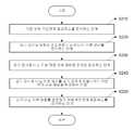
도 1a 및 1b는 본 발명의 일 실시예에 따른 도선 및 반도체 소자 배선용 나노 카본 재료 및 육방정계 질화붕소 적층구조물을 제조하는 방법의 순서도를 도시한다.
도 2a-2d는 본 발명의 일 실시예에 따른 도선 및 반도체 소자 배선용 나노 카본 재료 및 육방정계 질화붕소 적층구조물을 제조하는 방법의 측면도를 도시한다.
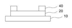
도 3은 본 발명의 추가적인 실시예에 따른 도선 및 반도체 소자 배선용 나노 카본 재료 및 육방정계 질화붕소 적층구조물의 측면도를 도시한다.
도 4는 본 발명의 일 실시예에 따른 도선 및 반도체 소자 배선용 나노 카본 재료 및 육방정계 질화붕소 적층구조물의 사시도를 도시한다.
도 5는 본 발명의 추가적인 실시예에 따른 도선 및 반도체 소자 배선용 나노 카본 재료 및 육방정계 질화붕소 적층구조물의 사시도를 도시한다.
도 6은 본 발명의 일 실시예에 따라 제작된 적층 구조물의 인가 전압 증가에 따른 온도 증가에 의한 저항값의 변화를 나타낸다.
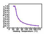
도 7은 본 발명의 일 실시예에 따라 제작된 적층 구조물의 온도에 따른 저항값을 정규화시킨 그래프이다.
다양한 실시예들이 이제 도면을 참조하여 설명되며, 전체 도면에서 걸쳐 유사한 도면번호는 유사한 엘리먼트를 나타내기 위해서 사용된다. 설명을 위해 본 명세서에서, 다양한 설명들이 본 발명의 이해를 제공하기 위해서 제시된다. 그러나 이러한 실시예들은 이러한 특정 설명 없이도 실행될 수 있음이 명백하다. 다른 예들에서, 공지된 구조 및 장치들은 실시예들의 설명을 용이하게 하기 위해서 블록 다이아그램 형태로 제시된다.FIGS. 1A and 1B show flowcharts of a method of manufacturing a nano-carbon material for a conductor and a semiconductor element wiring and a hexagonal boron nitride layered structure according to an embodiment of the present invention.
FIGS. 2A to 2D illustrate side views of a method of manufacturing a nano-carbon material for a wire and a semiconductor device wiring and a hexagonal boron nitride layered structure according to an embodiment of the present invention.
Fig. 3 shows a side view of a nano-carbon material for a conductor and a semiconductor element wiring and a hexagonal boron nitride laminated structure according to a further embodiment of the present invention.
4 is a perspective view of a nano carbon material for a conductor and a semiconductor device wiring and a hexagonal boron nitride laminated structure according to an embodiment of the present invention.
5 shows a perspective view of a nano-carbon material for a conductor and a semiconductor element wiring and a hexagonal boron nitride layered structure according to a further embodiment of the present invention.
FIG. 6 shows a change in resistance value due to an increase in temperature due to an increase in applied voltage of the laminated structure fabricated according to an embodiment of the present invention.
FIG. 7 is a graph illustrating a normalized resistance value of a stacked structure according to an exemplary embodiment of the present invention. Referring to FIG.
Various embodiments are now described with reference to the drawings, wherein like reference numerals are used throughout the drawings to refer to like elements. For purposes of explanation, various descriptions are set forth herein to provide an understanding of the present invention. It is evident, however, that such embodiments may be practiced without these specific details. In other instances, well-known structures and devices are shown in block diagram form in order to facilitate describing the embodiments.
하기 설명은 본 발명의 실시예에 대한 기본적인 이해를 제공하기 위해서 하나 이상의 실시예들의 간략화된 설명을 제공한다. 본 섹션은 모든 가능한 실시예들에 대한 포괄적인 개요는 아니며, 모든 엘리먼트들 중 핵심 엘리먼트를 식별하거나, 모든 실시예의 범위를 커버하고자 할 의도도 아니다. 그 유일한 목적은 후에 제시되는 상세한 설명에 대한 도입부로서 간략화된 형태로 하나 이상의 실시예들의 개념을 제공하기 위함이다.The following description provides a simplified description of one or more embodiments in order to provide a basic understanding of embodiments of the invention. This section is not a comprehensive overview of all possible embodiments and is not intended to identify key elements or to cover the scope of all embodiments of all elements. Its sole purpose is to present the concept of one or more embodiments in a simplified form as a prelude to the more detailed description that is presented later.
본 발명은 위에서 언급한 것처럼 기존의 도선의 경우 줄열로 인하여 도선의 온도가 높아지면, 도체의 포논과 결함의 진동은 더욱 커져 도선의 저항은 증가하게 되는 문제점 및 200~300℃ 이상의 온도에서 도선 내부의 도체들이 급속히 산화되는 문제점을 해결하기 위한 것이다. 이러한 발열과 산화의 문제들은 실리콘 기반의 반도체 소자에서 해결해야하는 큰 문제점이기 때문이다.As described above, in the case of a conventional lead wire, when the temperature of the lead wire is increased due to a juxtaposition, the vibration of the phonons and defects of the conductor is further increased to increase the resistance of the lead wire. In order to solve the problem of the rapid oxidation of the conductors. These heat and oxidation problems are a major problem to be solved in silicon-based semiconductor devices.
이러한 문제점을 해결하기 위해 본 발명에서는 나노 카본 재료와 육방정계 질화붕소의 이종 적층구조를 구현하고자 하였다. 이러한 적층 구조물을 통해, 본 발명의 발명자는 온도가 증가함에 따라 저항이 감소하는 특성을 보이는 배선(interconnection)을 제공하고자 한다.In order to solve such a problem, the present invention attempts to realize a hetero-laminated structure of nano-carbon material and hexagonal boron nitride. Through such a laminated structure, the inventor of the present invention intends to provide an interconnection exhibiting a characteristic of decreasing resistance as the temperature increases.
도 1a 및 1b는 본 발명의 일 실시예에 따른 도선 및 반도체 소자 배선용 나노 카본 재료 및 육방정계 질화붕소 적층구조물을 제조하는 방법의 순서도를 도시한다. 도 1a와 1b의 차이점은 도 1a의 경우에는 적층 구조물이 나노 카본 재료를 육방정계 질화붕소가 덮고 있는 형태인 반면에, 도 1b의 경우에는 나노 카본 재료를 육방정계 질화붕소가 위아래 샌드위치 형태로 덮고 있다는 점이다.FIGS. 1A and 1B show flowcharts of a method of manufacturing a nano-carbon material for a conductor and a semiconductor element wiring and a hexagonal boron nitride layered structure according to an embodiment of the present invention. The difference between FIGS. 1A and 1B is that in the case of FIG. 1A, the nano carbon material is covered with hexagonal boron nitride while the laminate structure is covered with the hexagonal boron nitride sandwich .
이하에서는 먼저 도 1a에 대해 설명하고 이후 도 1b를 설명하겠으며, 도 1a와 1b의 중복되는 부분의 설명은 도 1b의 설명에서 생략하도록 하겠다.Hereinafter, FIG. 1A will be described first, and FIG. 1B will be described later, and description of the overlapping portions of FIGS. 1A and 1B will be omitted from the description of FIG. 1B.
도 1a를 살펴보면, 본 발명의 일 실시예에 따른 도선 및 반도체 소자 배선용 나노 카본 재료 및 육방정계 질화붕소 적층구조물을 제조하는 방법은, 기판 상에 나노 카본 재료를 전사하는 단계(S 110); 상기 전사된 나노 카본 재료 상에 패턴된 전극을 형성하는 단계(S 120); 상기 전사된 나노 카본 재료를 상기 전극과 연결시키기 위한 전자 수송 채널을 형성하는 단계(S 130); 및 상기 나노 카본 재료를 보호하기 위해 육방정계 질화붕소를 전사하는 단계(S 140)를 포함한다.Referring to FIG. 1A, a method of fabricating a nano-carbon material and a hexagonal boron nitride layered structure for a conductor and a semiconductor device wiring according to an embodiment of the present invention includes: (S 110) transferring a nano-carbon material onto a substrate; Forming a patterned electrode on the transferred nanocarbon material (S 120); Forming an electron transport channel (S 130) for connecting the transferred nanocarbon material to the electrode; And transferring (S 140) hexagonal boron nitride to protect the nano-carbon material.
S 110 단계에서는 기판 상에 나노 카본 재료를 전사하는 단계로서, 먼저 기판을 준비하고 그 위에 나노 카본 재료를 전사하게 된다. 도 2a의 모습은 기판(10) 상에 나노 카본 재료(20)가 전사된 모습을 도시한다.In step S 110, the nano-carbon material is transferred onto the substrate. First, a substrate is prepared and the nano-carbon material is transferred onto the substrate. 2A shows a state in which the nano-
기판은 부도체 기판이 이용되는 것이 바람직하며, 구체적으로는 SiO2, Si3N4, SiC와 같은 실리콘 계열 기판과, PET, PEN, PES와 같은 플라스틱 폴리머 기판, PDMS, eco-flex와 같은 신축성 있는 폴리머 기판 등이 이용된다.It is preferable to use an insulating substrate such as a silicon substrate such as SiO2 , Si3 N4 , or SiC, a plastic polymer substrate such as PET, PEN, or PES, a flexible substrate such as PDMS, eco-flex A polymer substrate or the like is used.
나노 카본 재료는 2차원 구조의 물질로서 그래핀(graphene), CNT (carbon nano tube), GO (graphene oxide), RGO (reduced graphene oxide) 및 nc-G (nano crystalline graphene) 중 어느 하나 이상이다. 나노 카본 재료는 별도로 성장시켜 준비한 후, 이를 기판 상에 전사시키게 된다. 나노 카본 재료의 성장 방법에는 특별한 제한은 없으며 알려진 어떠한 방법을 이용해서도 성장 가능하다.The nano-carbon material is at least one of graphene, carbon nano tube, GO (graphene oxide), reduced graphene oxide (RGO), and nano crystalline graphene. The nano carbon material is separately grown and prepared, and then transferred onto the substrate. There is no particular limitation on the growth method of the nano-carbon material, and it is possible to grow using any known method.
S 120 단계에서는 전사된 나노 카본 재료 상에 패턴된 전극을 형성하는 단계이다. 도 2b는 나노 카본 재료(20) 상에 포토레지스트(30)를 형성한 이후 UV 노광을 거친 후 현상액을 이용해 전극이 올라갈 위치만 현상하게 되며, 도 2c에서처럼 전극 위치에 전극(40)이 증착된다.In
이러한 패턴된 전극의 형성은 포토리소그래피(photo-lithography), 전자 빔 증발(electron beam evaporation), 열 증발(thermal evaporation) 및 리프트 오프(lift-off) 중 어느 하나 이상의 방법을 이용하여 형성된다.The formation of such a patterned electrode is performed using at least one of a photo-lithography method, an electron beam evaporation method, a thermal evaporation method, and a lift-off method.
S 130 단계에서는 전사된 나노 카본 재료를 전극과 연결시키기 위한 전자 수송 채널을 형성한다. 전자 수송 채널의 형성은 포토리소그래피 및 산소 플라즈마 식각을 이용하여 형성된다.In step S 130, an electron transport channel for connecting the transferred nanocarbon material to the electrode is formed. The formation of the electron transport channel is formed using photolithography and oxygen plasma etching.
S 140 단계에서는 나노 카본 재료를 보호하기 위해 육방정계 질화붕소를 전사한다. 육방정계 질화붕소는 나노 카본 재료와는 반대로 부도체의 특성을 갖고 있으며, 화학적으로 안정적이다. 뿐만 아니라, 1000℃ 가까이 되는 고온에서도 그 형태를 유지할 수 있으므로 나노 카본 재료의 보호층으로 사용하기에 매우 적합한 물질이다.In step S 140, hexagonal boron nitride is transferred to protect the nano-carbon material. Hexavalent boron nitride has the characteristics of nonconductors as opposed to nano-carbon materials and is chemically stable. In addition, since it can maintain its shape even at a high temperature of about 1000 ° C., it is a material very suitable for use as a protective layer of nano-carbon materials.
도 1b에서는 육방정계 질화붕소(h-BN)가 샌드위치 형태로 나노 카본 재료의 위아래에 배치된 형태의 순서도를 도시한다. 도 1b에서와 같이 보호층으로 사용한 h-BN은 그래핀 하부에도 사용하여 샌드위치 구조 또한 가능하다. 도 3은 샌드위치 형태로 h-BN이 배치된 형태의 적층 구조물의 단면도를 도시한다.1B shows a flow chart of the form in which hexagonal boron nitride (h-BN) is placed in the sandwich form above and below the nano-carbon material. As shown in FIG. 1B, the h-BN used as the protective layer can also be used under the graphene, and a sandwich structure is also possible. 3 shows a cross-sectional view of a laminated structure in the form of h-BN disposed in sandwich form.
도 1b에서 도시된 본 발명의 추가적인 실시예에 따른 도선 및 반도체 소자 배선용 나노 카본 재료 및 육방정계 질화붕소 적층구조물의 제조 방법은, 기판 상에 육방정계 질화붕소를 전사하는 단계(S 210); 상기 전사된 육방정계 질화붕소 상에 나노 카본 재료를 전사하는 단계(S 220); 상기 전사된 나노 카본 재료 상에 패턴된 전극을 형성하는 단계(S 230); 상기 전사된 나노 카본 재료를 상기 전극과 연결시키기 위한 전자 수송 채널을 형성하는 단계(S 240); 및 상기 나노 카본 재료를 보호하기 위해 육방정계 질화붕소를 전사하는 단계(S 250)를 포함한다.The method for manufacturing a nano-carbon material and a hexagonal boron nitride layered structure for a conductor and a semiconductor device wiring according to a further embodiment of the present invention shown in FIG. 1B includes: (S 210) transferring hexagonal boron nitride from a substrate; Transferring the nano-carbon material onto the transferred hexagonal boron nitride (S 220); Forming a patterned electrode on the transferred nanocarbon material (S 230); Forming an electron transport channel (S 240) for connecting the transferred nanocarbon material to the electrode; And transferring the hexagonal boron nitride to protect the nano-carbon material (S 250).
본 발명의 일 실시예에 따른 도선 및 반도체 소자 배선용 나노 카본 재료 및 육방정계 질화붕소 적층구조물은, 기판(10); 상기 기판 상에 형성된 나노 카본 재료층(20); 상기 나노 카본 재료층 상에 형성된 전극 패턴(40); 및 상기 나노 카본 재료층을 덮는 육방정계 질화붕소층(50)을 포함한다. 이는 도 2d에서 도시되어 있다. 이러한 실시예의 사시도는 도 4에서 볼 수 있다.The nano-carbon material and the hexagonal boron nitride layered structure for wires and semiconductor device wiring according to an embodiment of the present invention include a
본 발명의 추가적인 실시예에 따른 도선 및 반도체 소자 배선용 나노 카본 재료 및 육방정계 질화붕소 적층구조물은, 기판(10); 상기 기판 상에 형성된 제 1 육방정계 질화붕소층(60); 상기 육방정계 질화붕소층 상의 나노 카본 재료층(20); 상기 나노 카본 재료층 상에 형성된 전극 패턴(40); 및 상기 나노 카본 재료층을 덮는 제 2 육방정계 질화붕소층(50)을 포함한다. 이는 도 3에서 도시되어 있다. 도 5는 샌드위치 형태의 실시예의 사시도를 도시한다.The nano-carbon material and the hexagonal boron nitride layered structure for wires and semiconductor device wiring according to a further embodiment of the present invention include a
본 발명에서는 위에서 설명한 도선 및 반도체 소자 배선용 나노 카본 재료 및 육방정계 질화붕소 적층구조물을 구현하였다. 본 발명의 발명자는 이러한 적층 구조물은 전기가 통할 때 반금속(semi-metal)의 특성을 보이는 나노 카본 재료가 온도가 증가함에 따라 저항이 감소하는 물리적인 특징에 착안, 나노 카본 재료를 이용한 배선과 그 배선을 감싸고 있는 동일한 2차원 구조인 육방정계 질화붕소를 절연피복으로 사용하는 구조를 만들었다.In the present invention, the above-described conductive wire, nano-carbon material for semiconductor device wiring, and hexagonal boron nitride laminated structure are implemented. The inventors of the present invention have found that such a laminated structure has a physical characteristic that a resistance of the nano-carbon material exhibiting semi-metal characteristics when electricity is increased decreases as the temperature increases, And a structure using hexagonal boron nitride, which is the same two-dimensional structure surrounding the wiring, as an insulating coating.
이하에서는 구체적인 실시예와 함께 본 발명의 내용을 추가적으로 설명하도록 하겠다.
Hereinafter, the contents of the present invention will be further described with reference to specific embodiments.
[실시예][Example]
본 발명의 발명자는 도 1a에서 설명한 것과 같은 단계에 따라서 도선 및 반도체 소자 배선용 나노 카본 재료 및 육방정계 질화붕소 적층구조물을 제조하였다.The inventors of the present invention have fabricated nano-carbon materials for wire and semiconductor device wiring and hexagonal boron nitride layered structure according to the same steps as described in FIG. 1A.
먼저 구리 호일(copper foil)을 촉매로 이용하여 나노 카본 재료 중 그래핀을 성장시키고, 이를 염화철(FeCl3) 용액으로 구리 호일을 식각한 후 습식 전사 방식을 이용하여 얻어진 그래핀을 부도체 기판인 SiO2에 전사하였다. 염화철(FeCl3) 용액으로 구리 호일이 완전히 제거되기 까지는 최소 20분 이상의 시간이 필요하므로 이를 육안으로 관찰하여 잔여 구리가 남아있는지 반드시 확인해야 한다. 만일 제거되지 않은 구리입자가 남아있게 되면, 이는 그래핀 소자의 특성을 떨어뜨리는 요인으로 작용할 수 있기 때문이다.First, graphene is grown in a nano-carbon material by using copper foil as a catalyst, and the copper foil is etched with a solution of iron chloride (FeCl3 ). Then, graphene obtained by a wet transfer method is applied to a non-2 . It takes at least 20 minutes to completely remove the copper foil from the ferric chloride solution (FeCl3 solution). Therefore, it is necessary to visually observe the remaining copper. If unremoved copper particles remain, this may cause degradation of the characteristics of the graphene device.
다음으로 네거티브 포토리소그래피(negative photo-lithography) 공정 또는 전자 빔 리소그래피(E-beam lithography) 공정을 이용하여 그래핀 소자(그래핀 배선)에 전원을 공급하기 위한 전극을 만들어주었다. 자외선에 반응하는 감광제인 포토레지스트(photoresist)(E-beam lithography의 경우 PMMA)를 샘플에 스핀코팅하여 그래핀 위에 균일하게 도포되도록 한 후, UV (E-beam lithography의 경우 전자빔)에 노광시켜주고 현생액을 이용하여 전극이 올라갈 위치만 부분적으로 현상하였다.Next, an electrode was prepared to supply the graphene device (graphene wiring) using a negative photo-lithography process or an electron beam lithography process. The photoresist (PMMA in the case of E-beam lithography), which is a photoresist that reacts with ultraviolet rays, is spin-coated on the sample to uniformly coat the same on graphene, and then exposed to UV (electron beam in the case of E-beam lithography) Only the position where the electrode rises was partially developed using the current solution.
이후 전자 빔 증발기(electron beam evaporator) 또는 열 증발기(thermal evaporator)를 이용하여 전극으로 사용할 티타늄(Ti)과 금(Au)를 각각 10nm이하, 50nm이상 증착하였다. 금속 전극으로 통상적으로 금을 가장 많이 사용하지만, 그래핀과 금 사이의 접착력이 굉장히 약하기 때문에 금과 접착력이 뛰어난 티타늄이나 크롬을 중간층으로 활용한다. 순서는 티타늄(TI)-금(Au) 순서로 증착시키며, 크롬과 금을 이용할 경우에는 크롬(Cr)-금(Au) 순으로 증착시켜 준다. 이때 티타늄의 두께는 10nm 이내로 해야 접촉저항을 줄일 수 있다. 이후, 아세톤을 이용하여 전원공급 전극 이외의 부분에 증착 된 금속들을 제거하는데, 이 과정을 리프트 오프(lift-off) 라고 하며, 아세톤(acetone)에 포토레지스트(photoresist) 와 PMMA가 녹는 원리를 이용하여 전극 이외의 부분에 올라간 티타늄(또는 크롬)-금 박막을 제거 하였다.Then, titanium (Ti) and gold (Au) used as an electrode were deposited to a thickness of 10 nm or less and 50 nm or more, respectively, by using an electron beam evaporator or a thermal evaporator. Although gold is the most commonly used metal electrode, the adhesion between graphene and gold is very weak, so titanium or chromium, which is superior in adhesion to gold, is used as an intermediate layer. The order is titanium (TI) - gold (Au) deposition. When chromium and gold are used, chromium (Cr) - gold (Au) are deposited in order. At this time, the thickness of titanium should be within 10 nm to reduce the contact resistance. Thereafter, acetone is used to remove metals deposited on portions other than the power supply electrode. This process is referred to as lift-off, and the principle of dissolving photoresist and PMMA in acetone is used To remove the titanium (or chromium) -gold thin film on the portion other than the electrode.
다음으로 전극과 연결 된 그래핀 채널 이외의 그래핀을 모두 제거하기 위하여 산소(O2) 플라즈마로 깎아내는 건식 식각방법을 이용하였다. 그래핀은 탄소원자들이 평면상에 단일층 으로만 결합하고 있는 구조이므로, 그 두께가 0.35~0.4nm 정도로 매우 얇기 때문에 식각 공정을 할 경우, 장비의 적절한 가스양과 압력, 식각시간을 잘 알고 있어야 한다. 그렇지 않을 경우, 원하지 않는 곳 까지 데미지를 줄 수 있다. 그래핀 식각을 위해 사용하는 플라즈마의 조건은 산소 5sccm 이상, RF Power는 20W 이상, 식각시간은 10초 이상으로 하며, 공정중의 작업 압력(working pressure)는 약 500mTorr 이하로 한다. 식각 후에는 그래핀 채널 위에 남아있는 잔여 포토레지스트를 아세톤으로 제거하였다.Next, a dry etching method is used in which an oxide (O2 ) plasma is used to remove graphene except for the graphene channel connected to the electrode. Since graphene is a structure in which carbon atoms are bonded in a single layer only on a plane, its thickness is very thin, about 0.35 to 0.4 nm. Therefore, when etching, it is necessary to know the proper amount of gas, pressure and etching time of the equipment . If not, you can do damage to where you do not want. The conditions of plasma used for graphene etching should be 5 sccm of oxygen, RF power of 20 W or more, etching time of 10 seconds or more, and the working pressure of the process should be less than 500 mTorr. After etching, the remaining photoresist remaining on the graphene channel was removed with acetone.
또한, 전극과 연결된 그래핀 채널을 형성하기 위하여, 포지티브 포토리소그래피(positive photo-lithography) (또는 전자 빔 리소그래피) 공정을 이용하여 선택적으로 노광을 한 후, 현상액을 이용하여 부분적으로 현상하였다.In addition, in order to form a graphene channel connected with the electrodes, selective exposure was performed using a positive photo-lithography (or electron beam lithography) process, and then partially developed using a developer.
마지막으로, 그래핀과 같은 구조를 갖고 있는 2차원 평면물질인 육방정계 질화붕소(h-BN)을 완성된 그래핀 배선 위에 전사하여 주었다. h-BN 또한 구리 호일 (Cu foil)에서 합성하므로, 그래핀과 같은 전사 방식인 습식 전사방식을 통하여 전사하였다.Finally, hexagonal boron nitride (h-BN), which is a two-dimensional planar material having the same structure as graphene, was transferred onto the completed graphene wiring. Since h-BN was also synthesized from copper foil, it was transferred through a wet transfer method such as graphene.
이러한 육방정계 질화붕소 (hexagonal boron bitride)는 그래핀을 보호하기 위한 부동태화(passivation)층과 외부와의 접촉을 차단하기 위한 절연층으로서 사용된다. 공기중에 노출 된 그래핀은 시간이 지남에 따라 표면에 산소원자와 -OH 작용기가 결합하게 되는데, 이는 그래핀의 성능을 저하시키는 요인으로 작용한다. h-BN은 그래핀과 동일한 2차원 구조를 지닌 물질로, 붕소(Boron)과 질소(Nitrogen) 원자가 3개씩 육각형 구조를 이루고 있다. 그 특성은 반 금속(semi-metal)인 그래핀과는 상이하게 다른 절연체(insulator)이다. 그래핀과의 격자 불일치가 약 1.7% 정도 이므로 그래핀 위쪽 표면을 덮거나 혹은 샌드위치 구조로 그래핀을 감싸서 사용하기에 최적의 조건을 갖춘 물질이다.This hexagonal boron bitride is used as a passivation layer for protecting graphene and an insulating layer for preventing contact with the outside. Over time, graphenes exposed to air become bound to oxygen atoms and -OH functional groups on the surface, which causes degradation of graphene performance. h-BN is a material having the same two-dimensional structure as graphene, and has three hexagonal structures of boron and nitrogen atoms. The characteristic is an insulator that differs from semi-metal graphene. Since the lattice mismatch with graphene is about 1.7%, it is the optimum material for covering the upper surface of graphene or wrapping graphene by sandwich structure.
도 6은 본 발명의 일 실시예에 따라 제작된 적층 구조물의 인가 전압 증가에 따른 온도 증가에 의한 저항값의 변화를 나타낸다. h-BN으로 그래핀 상부를 덮어서 보호층/절연층을 형성한 후, 전압(voltage bias)을 인가하여 그래핀 배선(interconnection)을 구동시키면 줄열 (Joule heating)에 의하여 그래핀에 열이 발생하게 된다. 인가전압을 점차 증가시킬 경우, 온도가 증가하며, 온도에 따른 저항값을 측정하였다. 도 6과 같이 온도가 증가함에 따라 그래핀의 저항은 감소함을 확인하였다.FIG. 6 shows a change in resistance value due to an increase in temperature due to an increase in applied voltage of the laminated structure fabricated according to an embodiment of the present invention. When graphene interconnection is driven by applying a voltage bias after covering the upper part of the graphene with h-BN, heat is generated in the graphene by joule heating do. When the applied voltage is gradually increased, the temperature increases and the resistance value according to the temperature is measured. As shown in FIG. 6, it was confirmed that the resistance of graphene decreased with increasing temperature.
일반적인 금속은 온도가 증가할수록, 전류의 흐름을 방해하는 저항이 증가하는 반면, 그래핀은 저항이 감소하게 된다. 이는 같은 전압을 걸어 주었을 때, 더 많은 전류를 수송할 수 있음을 의미한다. 또한, 그래핀을 이용하여 반도체 소자의 배선 또는 도선으로 사용할 경우, 줄열에 의하여 발생한 온도에서, 낮은 저항 때문에 더 많은 전류를 공급할 수 있다는 것은, 소자 구동이 더 원활하고 더 많은 정보를 처리할 수 있음을 의미한다.As the temperature of a typical metal increases, the resistance that impedes the flow of current increases, while the resistance of graphene decreases. This means that more current can be delivered when the same voltage is applied. In addition, when graphene is used as a wiring or a conductor of a semiconductor device, the ability to supply a larger amount of current due to a low resistance at a temperature generated by the joule heat can smoothly drive the device and process more information .
도 7은 본 발명의 일 실시예에 따라 제작된 적층 구조물의 온도에 따른 저항값을 정규화시킨 그래프이다.FIG. 7 is a graph illustrating a normalized resistance value of a stacked structure according to an exemplary embodiment of the present invention. Referring to FIG.
도 7을 살펴보면, 그래핀 소자의 온도가 200℃ 이상 도달했을때, 기준점보다 저항이 90% 가까이 감소함을 알 수 있다. 이는 h-BN없이 그래핀 만으로 배선을 만들었을 경우보다 훨씬 더 두드러진 결과이며, 그래핀을 이용한 도선 또는 배선을 만들 경우, h-BN을 반드시 이용해야 더 큰 효과를 얻을 수 있음을 의미한다.Referring to FIG. 7, when the temperature of the graphene device reaches 200 ° C or more, the resistance decreases by 90% from the reference point. This is much more noticeable than when graphene alone is used without h-BN, which means that h-BN must be used for graphene wires or wiring to achieve a greater effect.
제시된 실시예들에 대한 설명은 임의의 본 발명의 기술 분야에서 통상의 지식을 가진 자가 본 발명을 이용하거나 또는 실시할 수 있도록 제공된다. 이러한 실시예들에 대한 다양한 변형들은 본 발명의 기술 분야에서 통상의 지식을 가진 자에게 명백할 것이며, 여기에 정의된 일반적인 원리들은 본 발명의 범위를 벗어남이 없이 다른 실시예들에 적용될 수 있다. 그리하여, 본 발명은 여기에 제시된 실시예들로 한정되는 것이 아니라, 여기에 제시된 원리들 및 신규한 특징들과 일관되는 최광의의 범위에서 해석되어야 할 것이다.The description of the disclosed embodiments is provided to enable any person skilled in the art to make or use the present invention. Various modifications to these embodiments will be readily apparent to those skilled in the art, and the generic principles defined herein may be applied to other embodiments without departing from the scope of the invention. Thus, the present invention is not intended to be limited to the embodiments shown herein but is to be accorded the widest scope consistent with the principles and novel features presented herein.
Claims (10)
Translated fromKorean상기 전사된 나노 카본 재료 상에 패턴된 전극을 형성하는 단계;
상기 전사된 나노 카본 재료를 상기 전극과 연결시키기 위한 전자 수송 채널을 형성하는 단계; 및
상기 나노 카본 재료를 보호하기 위해 육방정계 질화붕소를 전사하는 단계를 포함하는,
도선 및 반도체 소자 배선용 나노 카본 재료 및 육방정계 질화붕소 적층구조물을 제조하는 방법.
Transferring the nano-carbon material onto the substrate;
Forming a patterned electrode on the transferred nanocarbon material;
Forming an electron transport channel for connecting the transferred nanocarbon material to the electrode; And
And transferring the hexagonal boron nitride to protect the nano-carbon material.
A method for manufacturing a nanocarbon material and a hexagonal boron nitride laminated structure for wire and semiconductor device wiring.
상기 전사된 육방정계 질화붕소 상에 나노 카본 재료를 전사하는 단계;
상기 전사된 나노 카본 재료 상에 패턴된 전극을 형성하는 단계;
상기 전사된 나노 카본 재료를 상기 전극과 연결시키기 위한 전자 수송 채널을 형성하는 단계; 및
상기 나노 카본 재료를 보호하기 위해 육방정계 질화붕소를 전사하는 단계를 포함하는,
도선 및 반도체 소자 배선용 나노 카본 재료 및 육방정계 질화붕소 적층구조물을 제조하는 방법.
Transferring hexagonal boron nitride onto the substrate;
Transferring the nano-carbon material onto the transferred hexagonal boron nitride;
Forming a patterned electrode on the transferred nanocarbon material;
Forming an electron transport channel for connecting the transferred nanocarbon material to the electrode; And
And transferring the hexagonal boron nitride to protect the nano-carbon material.
A method for manufacturing a nanocarbon material and a hexagonal boron nitride laminated structure for wire and semiconductor device wiring.
상기 전사된 나노 카본 재료 상에 패턴된 전극을 형성하는 단계는,
포토리소그래피(photo-lithography), 전자 빔 증발(electron beam evaporation), 열 증발(thermal evaporation) 및 리프트 오프(lift-off) 중 어느 하나 이상의 방법을 이용하여 형성하는 것을 특징으로 하는,
도선 및 반도체 소자 배선용 나노 카본 재료 및 육방정계 질화붕소 적층구조물을 제조하는 방법.
3. The method according to claim 1 or 2,
Wherein forming the patterned electrode on the transferred nanocarbon material comprises:
Characterized in that the film is formed using at least one of a photolithography method, an electron beam evaporation method, a thermal evaporation method, and a lift-off method.
A method for manufacturing a nanocarbon material and a hexagonal boron nitride laminated structure for wire and semiconductor device wiring.
상기 전자 수송 채널을 형성하는 단계는,
포토리소그래피 및 산소 플라즈마 식각을 이용하여 형성하는 것을 특징으로 하는,
도선 및 반도체 소자 배선용 나노 카본 재료 및 육방정계 질화붕소 적층구조물을 제조하는 방법.
3. The method according to claim 1 or 2,
Wherein forming the electron transport channel comprises:
Photolithography, and oxygen plasma etching.
A method for manufacturing a nanocarbon material and a hexagonal boron nitride laminated structure for wire and semiconductor device wiring.
상기 나노 카본 재료는 그래핀(graphene), CNT (carbon nano tube), GO (graphene oxide), RGO (reduced graphene oxide) 및 nc-G (nano crystalline graphene) 중 어느 하나 이상인 것을 특징으로 하는,
도선 및 반도체 소자 배선용 나노 카본 재료 및 육방정계 질화붕소 적층구조물을 제조하는 방법.
3. The method according to claim 1 or 2,
Wherein the nano-carbon material is at least one of graphene, carbon nanotube (CNT), graphene oxide (GO), reduced graphene oxide (RGO), and nano crystalline graphene.
A method for manufacturing a nanocarbon material and a hexagonal boron nitride laminated structure for wire and semiconductor device wiring.
상기 기판은 부도체 기판인 것을 특징으로 하는,
도선 및 반도체 소자 배선용 나노 카본 재료 및 육방정계 질화붕소 적층구조물을 제조하는 방법.
3. The method according to claim 1 or 2,
Characterized in that the substrate is an nonconductive substrate.
A method for manufacturing a nanocarbon material and a hexagonal boron nitride laminated structure for wire and semiconductor device wiring.
상기 기판 상에 형성된 나노 카본 재료층;
상기 나노 카본 재료층 상에 형성된 전극 패턴; 및
상기 나노 카본 재료층을 덮는 육방정계 질화붕소층을 포함하는,
도선 및 반도체 소자 배선용 나노 카본 재료 및 육방정계 질화붕소 적층구조물.
Board;
A nano-carbon material layer formed on the substrate;
An electrode pattern formed on the nano-carbon material layer; And
And a hexagonal boron nitride layer covering the nano-carbon material layer.
Nano - carbon materials and hexagonal boron nitride laminated structures for wire and semiconductor device wiring.
상기 기판 상에 형성된 제 1 육방정계 질화붕소층;
상기 육방정계 질화붕소층 상의 나노 카본 재료층;
상기 나노 카본 재료층 상에 형성된 전극 패턴; 및
상기 나노 카본 재료층을 덮는 제 2 육방정계 질화붕소층을 포함하는,
도선 및 반도체 소자 배선용 나노 카본 재료 및 육방정계 질화붕소 적층구조물.
Board;
A first hexagonal boron nitride layer formed on the substrate;
A nano-carbon material layer on the hexagonal boron nitride layer;
An electrode pattern formed on the nano-carbon material layer; And
And a second hexagonal boron nitride layer covering the nano-carbon material layer.
Nano - carbon materials and hexagonal boron nitride laminated structures for wire and semiconductor device wiring.
상기 나노 카본 재료는 그래핀(graphene), CNT (carbon nano tube), GO (graphene oxide), RGO (reduced graphene oxide) 및 nc-G (nano crystalline graphene) 중 어느 하나 이상인 것을 특징으로 하는,
도선 및 반도체 소자 배선용 나노 카본 재료 및 육방정계 질화붕소 적층구조물.
9. The method according to claim 7 or 8,
Wherein the nano-carbon material is at least one of graphene, carbon nanotube (CNT), graphene oxide (GO), reduced graphene oxide (RGO), and nano crystalline graphene.
Nano - carbon materials and hexagonal boron nitride laminated structures for wire and semiconductor device wiring.
상기 기판은 부도체 기판인 것을 특징으로 하는,
도선 및 반도체 소자 배선용 나노 카본 재료 및 육방정계 질화붕소 적층구조물.
9. The method according to claim 7 or 8,
Characterized in that the substrate is an nonconductive substrate.
Nano - carbon materials and hexagonal boron nitride laminated structures for wire and semiconductor device wiring.
Priority Applications (1)
| Application Number | Priority Date | Filing Date | Title |
|---|---|---|---|
| KR1020150037562AKR101685791B1 (en) | 2015-03-18 | 2015-03-18 | Stacked structure of nano carbon material and hexagonal boron nitride for leading wire and interconnection of semiconductors |
Applications Claiming Priority (1)
| Application Number | Priority Date | Filing Date | Title |
|---|---|---|---|
| KR1020150037562AKR101685791B1 (en) | 2015-03-18 | 2015-03-18 | Stacked structure of nano carbon material and hexagonal boron nitride for leading wire and interconnection of semiconductors |
Publications (2)
| Publication Number | Publication Date |
|---|---|
| KR20160112245Atrue KR20160112245A (en) | 2016-09-28 |
| KR101685791B1 KR101685791B1 (en) | 2016-12-13 |
Family
ID=57102039
Family Applications (1)
| Application Number | Title | Priority Date | Filing Date |
|---|---|---|---|
| KR1020150037562AExpired - Fee RelatedKR101685791B1 (en) | 2015-03-18 | 2015-03-18 | Stacked structure of nano carbon material and hexagonal boron nitride for leading wire and interconnection of semiconductors |
Country Status (1)
| Country | Link |
|---|---|
| KR (1) | KR101685791B1 (en) |
Cited By (6)
| Publication number | Priority date | Publication date | Assignee | Title |
|---|---|---|---|---|
| US10971451B2 (en) | 2018-07-24 | 2021-04-06 | Samsung Electronics Co., Ltd. | Interconnect structure having nanocrystalline graphene cap layer and electronic device including the interconnect structure |
| US11094538B2 (en) | 2018-10-01 | 2021-08-17 | Samsung Electronics Co., Ltd. | Method of forming graphene |
| US11149346B2 (en) | 2018-07-25 | 2021-10-19 | Samsung Electronics Co., Ltd. | Method of directly growing carbon material on substrate |
| US11180373B2 (en) | 2017-11-29 | 2021-11-23 | Samsung Electronics Co., Ltd. | Nanocrystalline graphene and method of forming nanocrystalline graphene |
| US11217531B2 (en) | 2018-07-24 | 2022-01-04 | Samsung Electronics Co., Ltd. | Interconnect structure having nanocrystalline graphene cap layer and electronic device including the interconnect structure |
| US11626282B2 (en) | 2019-04-30 | 2023-04-11 | Samsung Electronics Co., Ltd. | Graphene structure and method of forming graphene structure |
Families Citing this family (1)
| Publication number | Priority date | Publication date | Assignee | Title |
|---|---|---|---|---|
| KR102023106B1 (en) | 2017-02-20 | 2019-09-20 | 광운대학교 산학협력단 | Method for manufacturing spin coating based high quality solution-processed boron nitride thin film and its application in electronic devices |
Citations (4)
| Publication number | Priority date | Publication date | Assignee | Title |
|---|---|---|---|---|
| KR100791948B1 (en)* | 2006-09-27 | 2008-01-04 | 삼성전자주식회사 | Carbon nanotube wiring formation method and semiconductor device wiring formation method using the same |
| KR20100012590A (en)* | 2008-07-29 | 2010-02-08 | 동신대학교산학협력단 | Nano coaxially shielded cable prepared and process thereof |
| JP2011258917A (en)* | 2010-06-04 | 2011-12-22 | Pinecone Energies Inc | Light-emitting-diode array and method for manufacturing the same |
| JP2012235121A (en)* | 2011-04-29 | 2012-11-29 | Qinghua Univ | Method of manufacturing light-emitting diode |
- 2015
- 2015-03-18KRKR1020150037562Apatent/KR101685791B1/ennot_activeExpired - Fee Related
Patent Citations (4)
| Publication number | Priority date | Publication date | Assignee | Title |
|---|---|---|---|---|
| KR100791948B1 (en)* | 2006-09-27 | 2008-01-04 | 삼성전자주식회사 | Carbon nanotube wiring formation method and semiconductor device wiring formation method using the same |
| KR20100012590A (en)* | 2008-07-29 | 2010-02-08 | 동신대학교산학협력단 | Nano coaxially shielded cable prepared and process thereof |
| JP2011258917A (en)* | 2010-06-04 | 2011-12-22 | Pinecone Energies Inc | Light-emitting-diode array and method for manufacturing the same |
| JP2012235121A (en)* | 2011-04-29 | 2012-11-29 | Qinghua Univ | Method of manufacturing light-emitting diode |
Cited By (7)
| Publication number | Priority date | Publication date | Assignee | Title |
|---|---|---|---|---|
| US11180373B2 (en) | 2017-11-29 | 2021-11-23 | Samsung Electronics Co., Ltd. | Nanocrystalline graphene and method of forming nanocrystalline graphene |
| US10971451B2 (en) | 2018-07-24 | 2021-04-06 | Samsung Electronics Co., Ltd. | Interconnect structure having nanocrystalline graphene cap layer and electronic device including the interconnect structure |
| US11217531B2 (en) | 2018-07-24 | 2022-01-04 | Samsung Electronics Co., Ltd. | Interconnect structure having nanocrystalline graphene cap layer and electronic device including the interconnect structure |
| US11682622B2 (en) | 2018-07-24 | 2023-06-20 | Samsung Electronics Co., Ltd. | Interconnect structure having nanocrystalline graphene cap layer and electronic device including the interconnect structure |
| US11149346B2 (en) | 2018-07-25 | 2021-10-19 | Samsung Electronics Co., Ltd. | Method of directly growing carbon material on substrate |
| US11094538B2 (en) | 2018-10-01 | 2021-08-17 | Samsung Electronics Co., Ltd. | Method of forming graphene |
| US11626282B2 (en) | 2019-04-30 | 2023-04-11 | Samsung Electronics Co., Ltd. | Graphene structure and method of forming graphene structure |
Also Published As
| Publication number | Publication date |
|---|---|
| KR101685791B1 (en) | 2016-12-13 |
Similar Documents
| Publication | Publication Date | Title |
|---|---|---|
| KR101685791B1 (en) | Stacked structure of nano carbon material and hexagonal boron nitride for leading wire and interconnection of semiconductors | |
| Kang et al. | Inking elastomeric stamps with micro‐patterned, single layer graphene to create high‐performance OFETs | |
| Wang et al. | Clean-lifting transfer of large-area residual-free graphene films | |
| US9040958B2 (en) | Transistors and methods of manufacturing the same | |
| Wang et al. | Plasma-induced nanowelding of a copper nanowire network and its application in transparent electrodes and stretchable conductors | |
| Liu et al. | Large scale pattern graphene electrode for high performance in transparent organic single crystal field-effect transistors | |
| JP4967034B2 (en) | Circuit device in which graphene film and metal electrode are electrically joined | |
| US20150287787A1 (en) | Graphene Device And Method Of Fabricating A Graphene Device | |
| KR20110132246A (en) | Method for manufacturing field effect transistor, method for manufacturing field effect transistor and semiconductor graphene oxide | |
| TWI544645B (en) | Thin film transistor and preparation method thereof | |
| CN103718290A (en) | Heat-Dissipating Material And Method For Producing Same, And Electronic Device And Method For Producing Same | |
| US20110133284A1 (en) | Multiple carbon nanotube transfer and its applications for making high-performance carbon nanotube field-effect transistor (cnfet), transparent electrodes, and three-dimensional integration of cnfets | |
| TW201303064A (en) | Process for forming carbon film or inorganic material film on substrate | |
| US10008605B2 (en) | Connecting structure and method for manufacturing the same, and semiconductor device | |
| An et al. | Ultraclean transfer of CVD-grown graphene and its application to flexible organic photovoltaic cells | |
| KR102037469B1 (en) | Graphene electronic device and manufacturing method thereof | |
| JP2012138451A (en) | Circuit device having graphene film and metal electrode bonded electrically | |
| KR101919426B1 (en) | Graphene electronic device and Manufacturing method of the same | |
| CN103400859A (en) | Graphene-based tunneling field-effect transistor unit and array and forming method of array | |
| CN103904186A (en) | Semiconductor device based on graphene electrode and manufacturing method thereof | |
| CN102354668A (en) | Preparation method of carbon-based nanometer material transistor | |
| JP2012199305A (en) | Semiconductor device | |
| Basu et al. | Graphene-based electrodes for enhanced organic thin film transistors based on pentacene | |
| KR101505471B1 (en) | Transfer and adhesion technology of nano thin film | |
| TWI508171B (en) | Semiconductor element structure and method of manufacturing same |
Legal Events
| Date | Code | Title | Description |
|---|---|---|---|
| A201 | Request for examination | ||
| PA0109 | Patent application | St.27 status event code:A-0-1-A10-A12-nap-PA0109 | |
| PA0201 | Request for examination | St.27 status event code:A-1-2-D10-D11-exm-PA0201 | |
| E902 | Notification of reason for refusal | ||
| PE0902 | Notice of grounds for rejection | St.27 status event code:A-1-2-D10-D21-exm-PE0902 | |
| P11-X000 | Amendment of application requested | St.27 status event code:A-2-2-P10-P11-nap-X000 | |
| P13-X000 | Application amended | St.27 status event code:A-2-2-P10-P13-nap-X000 | |
| PG1501 | Laying open of application | St.27 status event code:A-1-1-Q10-Q12-nap-PG1501 | |
| E701 | Decision to grant or registration of patent right | ||
| PE0701 | Decision of registration | St.27 status event code:A-1-2-D10-D22-exm-PE0701 | |
| GRNT | Written decision to grant | ||
| PR0701 | Registration of establishment | St.27 status event code:A-2-4-F10-F11-exm-PR0701 | |
| PR1002 | Payment of registration fee | St.27 status event code:A-2-2-U10-U11-oth-PR1002 Fee payment year number:1 | |
| PG1601 | Publication of registration | St.27 status event code:A-4-4-Q10-Q13-nap-PG1601 | |
| R18-X000 | Changes to party contact information recorded | St.27 status event code:A-5-5-R10-R18-oth-X000 | |
| P22-X000 | Classification modified | St.27 status event code:A-4-4-P10-P22-nap-X000 | |
| FPAY | Annual fee payment | Payment date:20190905 Year of fee payment:4 | |
| PR1001 | Payment of annual fee | St.27 status event code:A-4-4-U10-U11-oth-PR1001 Fee payment year number:4 | |
| PR1001 | Payment of annual fee | St.27 status event code:A-4-4-U10-U11-oth-PR1001 Fee payment year number:5 | |
| PR1001 | Payment of annual fee | St.27 status event code:A-4-4-U10-U11-oth-PR1001 Fee payment year number:6 | |
| PR1001 | Payment of annual fee | St.27 status event code:A-4-4-U10-U11-oth-PR1001 Fee payment year number:7 | |
| PR1001 | Payment of annual fee | St.27 status event code:A-4-4-U10-U11-oth-PR1001 Fee payment year number:8 | |
| R18-X000 | Changes to party contact information recorded | St.27 status event code:A-5-5-R10-R18-oth-X000 | |
| PN2301 | Change of applicant | St.27 status event code:A-5-5-R10-R13-asn-PN2301 St.27 status event code:A-5-5-R10-R11-asn-PN2301 | |
| PC1903 | Unpaid annual fee | St.27 status event code:A-4-4-U10-U13-oth-PC1903 Not in force date:20241207 Payment event data comment text:Termination Category : DEFAULT_OF_REGISTRATION_FEE | |
| R18-X000 | Changes to party contact information recorded | St.27 status event code:A-5-5-R10-R18-oth-X000 | |
| PC1903 | Unpaid annual fee | St.27 status event code:N-4-6-H10-H13-oth-PC1903 Ip right cessation event data comment text:Termination Category : DEFAULT_OF_REGISTRATION_FEE Not in force date:20241207 |