KR20160107784A - Non volatile memory devices and methods of manufacturing the same - Google Patents
Non volatile memory devices and methods of manufacturing the sameDownload PDFInfo
- Publication number
- KR20160107784A KR20160107784AKR1020150031060AKR20150031060AKR20160107784AKR 20160107784 AKR20160107784 AKR 20160107784AKR 1020150031060 AKR1020150031060 AKR 1020150031060AKR 20150031060 AKR20150031060 AKR 20150031060AKR 20160107784 AKR20160107784 AKR 20160107784A
- Authority
- KR
- South Korea
- Prior art keywords
- pattern
- film pattern
- preliminary
- film
- air gap
- Prior art date
- Legal status (The legal status is an assumption and is not a legal conclusion. Google has not performed a legal analysis and makes no representation as to the accuracy of the status listed.)
- Granted
Links
Images


Classifications
- H—ELECTRICITY
- H01—ELECTRIC ELEMENTS
- H01L—SEMICONDUCTOR DEVICES NOT COVERED BY CLASS H10
- H01L21/00—Processes or apparatus adapted for the manufacture or treatment of semiconductor or solid state devices or of parts thereof
- H01L21/70—Manufacture or treatment of devices consisting of a plurality of solid state components formed in or on a common substrate or of parts thereof; Manufacture of integrated circuit devices or of parts thereof
- H01L21/71—Manufacture of specific parts of devices defined in group H01L21/70
- H01L21/76—Making of isolation regions between components
- H01L21/762—Dielectric regions, e.g. EPIC dielectric isolation, LOCOS; Trench refilling techniques, SOI technology, use of channel stoppers
- H01L21/7624—Dielectric regions, e.g. EPIC dielectric isolation, LOCOS; Trench refilling techniques, SOI technology, use of channel stoppers using semiconductor on insulator [SOI] technology
- H01L21/76264—SOI together with lateral isolation, e.g. using local oxidation of silicon, or dielectric or polycristalline material refilled trench or air gap isolation regions, e.g. completely isolated semiconductor islands
- H01L21/76289—Lateral isolation by air gap
- H01L27/11521—
- H—ELECTRICITY
- H01—ELECTRIC ELEMENTS
- H01L—SEMICONDUCTOR DEVICES NOT COVERED BY CLASS H10
- H01L21/00—Processes or apparatus adapted for the manufacture or treatment of semiconductor or solid state devices or of parts thereof
- H01L21/02—Manufacture or treatment of semiconductor devices or of parts thereof
- H01L21/04—Manufacture or treatment of semiconductor devices or of parts thereof the devices having potential barriers, e.g. a PN junction, depletion layer or carrier concentration layer
- H01L21/18—Manufacture or treatment of semiconductor devices or of parts thereof the devices having potential barriers, e.g. a PN junction, depletion layer or carrier concentration layer the devices having semiconductor bodies comprising elements of Group IV of the Periodic Table or AIIIBV compounds with or without impurities, e.g. doping materials
- H01L21/30—Treatment of semiconductor bodies using processes or apparatus not provided for in groups H01L21/20 - H01L21/26
- H01L21/31—Treatment of semiconductor bodies using processes or apparatus not provided for in groups H01L21/20 - H01L21/26 to form insulating layers thereon, e.g. for masking or by using photolithographic techniques; After treatment of these layers; Selection of materials for these layers
- H01L21/3105—After-treatment
- H01L21/31051—Planarisation of the insulating layers
- H01L21/31053—Planarisation of the insulating layers involving a dielectric removal step
- H01L21/31055—Planarisation of the insulating layers involving a dielectric removal step the removal being a chemical etching step, e.g. dry etching
- H—ELECTRICITY
- H01—ELECTRIC ELEMENTS
- H01L—SEMICONDUCTOR DEVICES NOT COVERED BY CLASS H10
- H01L21/00—Processes or apparatus adapted for the manufacture or treatment of semiconductor or solid state devices or of parts thereof
- H01L21/70—Manufacture or treatment of devices consisting of a plurality of solid state components formed in or on a common substrate or of parts thereof; Manufacture of integrated circuit devices or of parts thereof
- H01L21/71—Manufacture of specific parts of devices defined in group H01L21/70
- H01L21/76—Making of isolation regions between components
- H01L21/762—Dielectric regions, e.g. EPIC dielectric isolation, LOCOS; Trench refilling techniques, SOI technology, use of channel stoppers
- H—ELECTRICITY
- H01—ELECTRIC ELEMENTS
- H01L—SEMICONDUCTOR DEVICES NOT COVERED BY CLASS H10
- H01L21/00—Processes or apparatus adapted for the manufacture or treatment of semiconductor or solid state devices or of parts thereof
- H01L21/70—Manufacture or treatment of devices consisting of a plurality of solid state components formed in or on a common substrate or of parts thereof; Manufacture of integrated circuit devices or of parts thereof
- H01L21/71—Manufacture of specific parts of devices defined in group H01L21/70
- H01L21/76—Making of isolation regions between components
- H01L21/764—Air gaps
- H—ELECTRICITY
- H10—SEMICONDUCTOR DEVICES; ELECTRIC SOLID-STATE DEVICES NOT OTHERWISE PROVIDED FOR
- H10B—ELECTRONIC MEMORY DEVICES
- H10B41/00—Electrically erasable-and-programmable ROM [EEPROM] devices comprising floating gates
- H10B41/30—Electrically erasable-and-programmable ROM [EEPROM] devices comprising floating gates characterised by the memory core region
- H—ELECTRICITY
- H10—SEMICONDUCTOR DEVICES; ELECTRIC SOLID-STATE DEVICES NOT OTHERWISE PROVIDED FOR
- H10D—INORGANIC ELECTRIC SEMICONDUCTOR DEVICES
- H10D30/00—Field-effect transistors [FET]
- H10D30/01—Manufacture or treatment
- H10D30/021—Manufacture or treatment of FETs having insulated gates [IGFET]
- H10D30/0411—Manufacture or treatment of FETs having insulated gates [IGFET] of FETs having floating gates
- H—ELECTRICITY
- H10—SEMICONDUCTOR DEVICES; ELECTRIC SOLID-STATE DEVICES NOT OTHERWISE PROVIDED FOR
- H10D—INORGANIC ELECTRIC SEMICONDUCTOR DEVICES
- H10D64/00—Electrodes of devices having potential barriers
- H10D64/01—Manufacture or treatment
- H10D64/031—Manufacture or treatment of data-storage electrodes
- H10D64/035—Manufacture or treatment of data-storage electrodes comprising conductor-insulator-conductor-insulator-semiconductor structures
- H—ELECTRICITY
- H10—SEMICONDUCTOR DEVICES; ELECTRIC SOLID-STATE DEVICES NOT OTHERWISE PROVIDED FOR
- H10D—INORGANIC ELECTRIC SEMICONDUCTOR DEVICES
- H10D84/00—Integrated devices formed in or on semiconductor substrates that comprise only semiconducting layers, e.g. on Si wafers or on GaAs-on-Si wafers
- H10D84/01—Manufacture or treatment
- H10D84/0123—Integrating together multiple components covered by H10D12/00 or H10D30/00, e.g. integrating multiple IGBTs
- H10D84/0126—Integrating together multiple components covered by H10D12/00 or H10D30/00, e.g. integrating multiple IGBTs the components including insulated gates, e.g. IGFETs
- H10D84/0144—Manufacturing their gate insulating layers
- H—ELECTRICITY
- H10—SEMICONDUCTOR DEVICES; ELECTRIC SOLID-STATE DEVICES NOT OTHERWISE PROVIDED FOR
- H10D—INORGANIC ELECTRIC SEMICONDUCTOR DEVICES
- H10D84/00—Integrated devices formed in or on semiconductor substrates that comprise only semiconducting layers, e.g. on Si wafers or on GaAs-on-Si wafers
- H10D84/01—Manufacture or treatment
- H10D84/0123—Integrating together multiple components covered by H10D12/00 or H10D30/00, e.g. integrating multiple IGBTs
- H10D84/0126—Integrating together multiple components covered by H10D12/00 or H10D30/00, e.g. integrating multiple IGBTs the components including insulated gates, e.g. IGFETs
- H10D84/0151—Manufacturing their isolation regions
- H—ELECTRICITY
- H10—SEMICONDUCTOR DEVICES; ELECTRIC SOLID-STATE DEVICES NOT OTHERWISE PROVIDED FOR
- H10D—INORGANIC ELECTRIC SEMICONDUCTOR DEVICES
- H10D84/00—Integrated devices formed in or on semiconductor substrates that comprise only semiconducting layers, e.g. on Si wafers or on GaAs-on-Si wafers
- H10D84/01—Manufacture or treatment
- H10D84/02—Manufacture or treatment characterised by using material-based technologies
- H10D84/03—Manufacture or treatment characterised by using material-based technologies using Group IV technology, e.g. silicon technology or silicon-carbide [SiC] technology
- H10D84/038—Manufacture or treatment characterised by using material-based technologies using Group IV technology, e.g. silicon technology or silicon-carbide [SiC] technology using silicon technology, e.g. SiGe
- H—ELECTRICITY
- H01—ELECTRIC ELEMENTS
- H01L—SEMICONDUCTOR DEVICES NOT COVERED BY CLASS H10
- H01L2924/00—Indexing scheme for arrangements or methods for connecting or disconnecting semiconductor or solid-state bodies as covered by H01L24/00
- H01L2924/10—Details of semiconductor or other solid state devices to be connected
- H01L2924/11—Device type
- H01L2924/14—Integrated circuits
- H01L2924/143—Digital devices
- H01L2924/1434—Memory
- H01L2924/1435—Random access memory [RAM]
- H01L2924/1443—Non-volatile random-access memory [NVRAM]
Landscapes
- Engineering & Computer Science (AREA)
- Microelectronics & Electronic Packaging (AREA)
- Condensed Matter Physics & Semiconductors (AREA)
- General Physics & Mathematics (AREA)
- Manufacturing & Machinery (AREA)
- Computer Hardware Design (AREA)
- Physics & Mathematics (AREA)
- Power Engineering (AREA)
- Non-Volatile Memory (AREA)
- Semiconductor Memories (AREA)
- Chemical & Material Sciences (AREA)
- Chemical Kinetics & Catalysis (AREA)
- General Chemical & Material Sciences (AREA)
Abstract
Translated fromKoreanDescription
Translated fromKorean본 발명은 비휘발성 메모리 소자 및 그 제조 방법에 관한 것이다. 보다 상세하게는, 본 발명은 에어 갭을 갖는 비휘발성 메모리 소자 및 그 제조 방법에 관한 것이다.The present invention relates to a nonvolatile memory device and a method of manufacturing the same. More particularly, the present invention relates to a nonvolatile memory device having an air gap and a method of manufacturing the same.
비휘발성 메모리 소자의 고집적화에 따라, 배선 라인들, 게이트 전극들 및 액티브 영역들 사이에서 기생 커패시턴스가 증가된다. 이에 따라, 기생 커패시턴스가 감소되는 비휘발성 메모리 소자 및 그 제조 방법이 요구된다.As the non-volatile memory device is highly integrated, the parasitic capacitance is increased between the wiring lines, the gate electrodes and the active regions. Accordingly, there is a demand for a nonvolatile memory device in which parasitic capacitance is reduced, and a manufacturing method thereof.
본 발명의 과제는 기생 커패시턴스가 감소되는 비휘발성 메모리 소자의 제조 방법을 제공하는 것이다.SUMMARY OF THE INVENTION The present invention provides a method of manufacturing a nonvolatile memory device in which parasitic capacitance is reduced.
본 발명의 과제는 상기한 비휘발성 메모리 소자를 제공하는 것이다.The present invention provides a nonvolatile memory device as described above.
상기한 과제를 달성하기 위한 본 발명의 일 실시예에 따른 반도체 소자의 제조 방법으로, 기판에 포함되는 제1 방향으로 연장되는 액티브 패턴 상에 예비 터널 절연막 패턴, 예비 전하 저장 패턴을 형성한다. 상기 예비 전하 저장 패턴, 터널 절연막 패턴 및 액티브 패턴 사이의 트렌치 표면에 라이너막을 형성한다. 상기 라이너막 상에 상기 트렌치의 일부를 채우는 예비 소자 분리막 패턴을 형성한다. 상기 예비 전하 저장 패턴 및 상기 예비 소자 분리막 패턴 상에 유전막 및 콘트롤 게이트 전극막을 형성한다. 상기 콘트롤 게이트 전극막, 상기 유전막, 상기 예비 전하 저장 패턴 및 상기 예비 터널 절연막 패턴을 패터닝하여 터널 절연막 패턴, 전하 저장 패턴, 유전막 패턴 및 콘트롤 게이트 전극이 적층되고, 상기 콘트롤 게이트 전극은 상기 제1 방향과 수직한 제2 방향으로 연장되는 게이트 구조물들을 형성한다. 상기 예비 소자 분리막 패턴의 일부를 등방성 건식 식각을 통해 제거하여, 소자 분리막 패턴 및 상기 소자 분리막 패턴 상에 제1 에어 갭을 형성하고, 상기 제1 에어 갭은 상기 제1 방향으로 연장되고 상부면에 굴곡을 포함하고, 상기 게이트 구조물 하부면과 소자 분리막 패턴의 상부면 사이 부위에서는 상기 기판 표면에 수직한 제3 방향으로의 제1 길이가 상기 제2 방향으로의 제1 폭보다 더 큰 형상을 갖도록 형성한다. 그리고, 상기 제1 에어 갭을 유지하면서, 상기 게이트 구조물들 사이에 층간 절연막을 형성한다.According to another aspect of the present invention, there is provided a method of manufacturing a semiconductor device, including: forming a preliminary tunnel insulating film pattern and a preliminary charge storage pattern on an active pattern extending in a first direction included in a substrate; A liner film is formed on the surface of the trench between the preliminary charge storage pattern, the tunnel insulating film pattern, and the active pattern. And a spare element isolation film pattern is formed on the liner film to fill a part of the trench. A dielectric film and a control gate electrode film are formed on the preliminary charge storage pattern and the preliminary element isolation film pattern. A tunnel insulating film pattern, a charge storage pattern, a dielectric film pattern, and a control gate electrode are laminated by patterning the control gate electrode film, the dielectric film, the pre-charge storage pattern, and the preliminary tunnel insulating film pattern, Lt; RTI ID = 0.0 > direction. ≪ / RTI > Wherein a part of the spare element separation film pattern is removed through isotropic dry etching to form a first air gap on the element separation film pattern and the element separation film pattern, and the first air gap extends in the first direction, Wherein a first length in a third direction perpendicular to the surface of the substrate is greater than a first width in the second direction at a portion between the lower surface of the gate structure and the upper surface of the device isolation film pattern . An interlayer insulating film is formed between the gate structures while maintaining the first air gap.
본 발명의 일 실시예에서, 상기 소자 분리막 패턴은 상기 터널 절연막 패턴 및 유전막 패턴에 포함되는 실리콘 산화물에 비해 다공성을 갖는 실리콘 산화물을 포함하도록 형성될 수 있다.In one embodiment of the present invention, the device isolation film pattern may be formed to include silicon oxide having porosity as compared with silicon oxide included in the tunnel insulating film pattern and the dielectric film pattern.
본 발명의 일 실시예에서, 상기 소자 분리막 패턴은 스핀온 글라스 물질을 포함하도록 형성될 수 있다.In one embodiment of the present invention, the device isolation film pattern may be formed to include a spin-on glass material.
본 발명의 일 실시예에서, 상기 터널 절연막 패턴 및 유전막 패턴에 포함되는 실리콘 산화물은 열산화 공정, 화학 기상 증착 공정 또는 고밀도 플라즈마 화학 기상 증착(HDP-CVD)공정을 통해 형성될 수 있다.In one embodiment of the present invention, the silicon oxide included in the tunnel insulating film pattern and the dielectric film pattern may be formed through a thermal oxidation process, a chemical vapor deposition process, or a high density plasma chemical vapor deposition (HDP-CVD) process.
본 발명의 일 실시예에서, 상기 등방성 건식 식각은 불소를 포함하는 가스 및 기상 상태의 H2O를 식각 가스로 함께 사용하여 수행할 수 있다.In one embodiment of the present invention, the isotropic dry etching may be performed using a fluorine-containing gas and H2 O in a gaseous state together as an etch gas.
본 발명의 일 실시예에서, 상기 불소를 포함하는 가스는 CxFy 또는 CHxFy를 포함할 수 있다.In one embodiment of the present invention, the fluorine-containing gas may comprise CxFy or CHxFy.
본 발명의 일 실시예에서, 상기 등방성 건식 식각은, 상기 기상 상태의 H2O를 식각 가스를 상기 예비 소자 분리막 패턴에 선택적으로 흡습시킨다. 상기 흡습된 예비 소자 분리막 패턴의 일부를 불소를 포함하는 가스를 이용하여 제거한다.In one embodiment of the present invention, in the isotropic dry etching, H2 O in the gaseous state is selectively absorbed by the etching gas to the preliminary element isolation film pattern. A part of the moisture-absorbing preliminary element isolation film pattern is removed by using a gas containing fluorine.
본 발명의 일 실시예에서, 상기 등방성 건식 식각은 5 내지 50도의 온도에서 수행될 수 있다.In one embodiment of the present invention, the isotropic dry etch may be performed at a temperature of 5 to 50 degrees.
본 발명의 일 실시예에서, 상기 소자 분리막 패턴은 상기 액티브 패턴의 높이의 70%보다 낮게 되도록 형성할 수 있다.In one embodiment of the present invention, the device isolation film pattern may be formed to be lower than 70% of the height of the active pattern.
본 발명의 일 실시예에서, 상기 게이트 구조물들 사이에 층간 절연막은 상기 층간 절연막 아래에 상기 제1 에어 갭과 연통하는 제2 에어 갭을 더 포함하도록 형성될 수 있다.In an embodiment of the present invention, an interlayer insulating film between the gate structures may be formed to further include a second air gap under the interlayer insulating film in communication with the first air gap.
상기한 과제를 달성하기 위한 본 발명의 일 실시예에 따른 반도체 소자는, 각각 제1 방향으로 연장되고 상기 제1 방향에 수직한 제2 방향을 따라 반복적으로 형성된 액티브 패턴들을 포함하는 기판 상에, 터널 절연막 패턴, 전하 저장, 유전막 패턴 및 콘트롤 게이트 전극을 포함하고, 상기 콘트롤 게이트 전극이 상기 제2 방향으로 연장되는 복수 개의 게이트 구조물들이 구비된다. 상기 액티브 패턴들 사이의 트렌치 표면 상에 라이너막이 구비된다. 상기 라이너막 상에 상기 액티브 패턴들 사이의 트렌치를 부분적으로 채우고, 상기 유전막 패턴과 이격되도록 배치되고, 상기 라이너막과 다른 물질을 포함하는 소자 분리막 패턴이 구비되고, 상기 소자 분리막 패턴 상에는 제1 에어 갭을 포함하고, 상기 제1 에어 갭은 상부면에 굴곡을 포함하고 상기 제1 방향으로 연장되고, 상기 게이트 구조물 하부면과 소자 분리막 패턴의 상부면 사이 부위에서는 상기 기판 표면에 수직한 제3 방향으로의 제1 길이가 상기 제2 방향으로의 제1 폭보다 더 큰 형상을 갖는다.According to an aspect of the present invention, there is provided a semiconductor device including: a substrate including active patterns extending in a first direction and repeatedly formed along a second direction perpendicular to the first direction; A plurality of gate structures including a tunnel insulating film pattern, a charge storage, a dielectric film pattern, and a control gate electrode, wherein the control gate electrode extends in the second direction. A liner film is provided on the trench surface between the active patterns. A device isolation film pattern partially filling the trench between the active patterns on the liner film and spaced apart from the dielectric film pattern and including a material different from the liner film; Wherein the first air gap includes a curvature in an upper surface and extends in the first direction, and in a region between a lower surface of the gate structure and an upper surface of the device isolation film pattern, Has a shape larger than the first width in the second direction.
본 발명의 일 실시예에서, 상기 소자 분리막 패턴과 유전막 패턴 사이에서, 상기 제1 에어 갭의 상, 하부는 라운드 형상을 갖고, 상기 제2 방향으로 절단한 단면은 타원 형상을 갖는다.In one embodiment of the present invention, between the device isolation film pattern and the dielectric film pattern, the upper and lower portions of the first air gap have a round shape, and the cross section cut in the second direction has an elliptical shape.
본 발명의 일 실시예에서, 상기 소자 분리막 패턴은 상기 터널 절연막 패턴 및 유전막 패턴에 포함되는 실리콘 산화물에 비해 다공성을 갖는 실리콘 산화물을 포함할 수 있다.In one embodiment of the present invention, the device isolation film pattern may include silicon oxide having porosity as compared with silicon oxide included in the tunnel insulating film pattern and the dielectric film pattern.
본 발명의 일 실시예에서, 상기 소자 분리막 패턴과 유전막 패턴 사이에서, 상기 제1 에어 갭의 상기 제3 방향의 제1 길이는 상기 제2 방향의 제1 폭의 1.5배 내지 6배일 수 있다.In one embodiment of the present invention, between the device isolation film pattern and the dielectric film pattern, the first length of the first air gap in the third direction may be 1.5 to 6 times the first width in the second direction.
본 발명의 일 실시예에서, 상기 소자 분리막 패턴의 상부면은 상기 게이트 구조물의 제1 방향 중심부와 대향하는 부위에서 상대적으로 높게 돌출되면서 굴곡된 형상을 가질 수 있다.In an embodiment of the present invention, the upper surface of the device isolation film pattern may have a curved shape while protruding relatively high at a portion facing the center portion in the first direction of the gate structure.
설명한 것과 같이, 본 발명에 따른 비휘발성 메모리 소자는 액티브 패턴들 사이 및 전하 저장 패턴들 사이에 에어 갭이 포함된다. 따라서, 상기 액티브 영역들 사이의 기생 커패시턴스 및 전하 저장 패턴 사이의 기생 커패시턴스를 감소시킬 수 있다. 또한, 터널 절연막 패턴 및 유전막 패턴의 손상이 억제된다. 따라서, 비휘발성 메모리 소자는 우수한 특성을 가질 수 있다.As described, a non-volatile memory device according to the present invention includes an air gap between active patterns and between charge storage patterns. Thus, the parasitic capacitance between the active regions and the parasitic capacitance between the charge storage patterns can be reduced. Further, damage to the tunnel insulating film pattern and the dielectric film pattern is suppressed. Therefore, the nonvolatile memory element can have excellent characteristics.
도 1 내지 3은 본 발명의 실시예 1에 따른 비휘발성 메모리 소자를 설명하기 위한 사시도, 단면도 및 평면도이다.
도 4 내지 도 12는 도 1 내지 도 3에 도시된 비휘발성 메모리 소자의 제조 방법을 설명하기 위한 단면도들 및 사시도들이다.
도 13은 본 발명의 실시예 2에 따른 비휘발성 메모리 소자를 설명하기 위한 사시도이다.
도 14는 본 발명의 실시예 3에 따른 비휘발성 메모리 소자를 설명하기 위한 사시도이다.
도 15는 본 발명의 실시예 4에 따른 비휘발성 메모리 소자를 설명하기 위한 사시도이다.
도 16 및 17은 본 발명의 실시예 5에 따른 비휘발성 메모리 소자를 설명하기 위한 사시도 및 단면도이다.
도 18 내지 도 21은 도 16에 도시된 비휘발성 메모리 소자의 제조 방법을 설명하기 위한 단면도 및 사시도들이다.
도 22는 예시적인 실시예들에 따른 시스템의 개략적인 구성을 나타내는 블록도이다.1 to 3 are a perspective view, a cross-sectional view, and a plan view for explaining a nonvolatile memory device according to a first embodiment of the present invention.
FIGS. 4 to 12 are cross-sectional views and perspective views illustrating a method of manufacturing the non-volatile memory device shown in FIGS.
13 is a perspective view illustrating a nonvolatile memory device according to a second embodiment of the present invention.
14 is a perspective view for explaining a nonvolatile memory device according to a third embodiment of the present invention.
15 is a perspective view for explaining a nonvolatile memory device according to a fourth embodiment of the present invention.
16 and 17 are a perspective view and a cross-sectional view for explaining a nonvolatile memory device according to a fifth embodiment of the present invention.
18 to 21 are a cross-sectional view and a perspective view for explaining the method of manufacturing the nonvolatile memory device shown in FIG.
22 is a block diagram illustrating a schematic configuration of a system according to exemplary embodiments.
이하, 첨부한 도면을 참조하여 본 발명의 바람직한 실시예를 상세히 설명하고자 한다.Hereinafter, preferred embodiments of the present invention will be described in detail with reference to the accompanying drawings.
본 발명의 각 도면에 있어서, 구조물들의 치수는 본 발명의 명확성을 기하기 위하여 실제보다 확대하여 도시한 것이다.In the drawings of the present invention, the dimensions of the structures are enlarged to illustrate the present invention in order to clarify the present invention.
본 발명에서, 제1, 제2 등의 용어는 다양한 구성요소들을 설명하는데 사용될 수 있지만, 상기 구성요소들은 상기 용어들에 의해 한정되어서는 안 된다. 상기 용어들은 하나의 구성요소를 다른 구성요소로부터 구별하는 목적으로만 사용된다.In the present invention, the terms first, second, etc. may be used to describe various elements, but the elements should not be limited by the terms. The terms are used only for the purpose of distinguishing one component from another.
본 발명에서 사용한 용어는 단지 특정한 실시예를 설명하기 위해 사용된 것으로, 본 발명을 한정하려는 의도가 아니다. 단수의 표현은 문맥상 명백하게 다르게 뜻하지 않는 한, 복수의 표현을 포함한다. 본 출원에서, "포함하다" 또는 "가지다" 등의 용어는 명세서 상에 기재된 특징, 숫자, 단계, 동작, 구성요소, 부품 또는 이들을 조합한 것이 존재함을 지정하려는 것이지, 하나 또는 그 이상의 다른 특징들이나 숫자, 단계, 동작, 구성요소, 부품 또는 이들을 조합한 것들의 존재 또는 부가 가능성을 미리 배제하지 않는 것으로 이해되어야 한다.The terminology used herein is for the purpose of describing particular embodiments only and is not intended to be limiting of the invention. The singular expressions include plural expressions unless the context clearly dictates otherwise. In the present application, the terms "comprises" or "having" and the like are used to specify that there is a feature, a number, a step, an operation, an element, a component or a combination thereof described in the specification, But do not preclude the presence or addition of one or more other features, integers, steps, operations, elements, components, or combinations thereof.
본 발명에 있어서, 각 층(막), 영역, 전극, 패턴 또는 구조물들이 대상체, 기판, 각 층(막), 영역, 전극 또는 패턴들의 "상에", "상부에" 또는 "하부"에 형성되는 것으로 언급되는 경우에는 각 층(막), 영역, 전극, 패턴 또는 구조물들이 직접 기판, 각 층(막), 영역, 또는 패턴들 위에 형성되거나 아래에 위치하는 것을 의미하거나, 다른 층(막), 다른 영역, 다른 전극, 다른 패턴 또는 다른 구조물들이 대상체나 기판 상에 추가적으로 형성될 수 있다. 또한, 물질, 층(막), 영역, 전극, 패턴들 또는 구조물들이 "제1", "제2" 및/또는 "예비"로 언급되는 경우, 이러한 부재들을 한정하기 위한 것이 아니라 단지 각 물질, 층(막), 영역, 전극, 패턴들 또는 구조물들을 구분하기 위한 것이다. 따라서 "제1", "제2" 및/또는 "예비"는 각 층(막), 영역, 전극, 패턴들 또는 구조물들에 대하여 각기 선택적으로 또는 교환적으로 사용될 수 있다.
In the present invention, it is to be understood that each layer (film), region, electrode, pattern or structure may be formed on, over, or under the object, substrate, layer, Means that each layer (film), region, electrode, pattern or structure is directly formed or positioned below a substrate, each layer (film), region, or pattern, , Other regions, other electrodes, other patterns, or other structures may additionally be formed on the object or substrate. It will also be understood that when a material, layer, area, electrode, pattern or structure is referred to as a "first", "second" and / or " Regions, electrodes, patterns, or structures. ≪ RTI ID = 0.0 > Thus, "first "," second "and / or" reserve "may be used, respectively, selectively or interchangeably for each layer (membrane), region, electrode, patterns or structures.
실시예 1Example 1
도 1 내지 3은 본 발명의 실시예 1에 따른 비휘발성 메모리 소자를 설명하기 위한 사시도, 단면도 및 평면도이다.1 to 3 are a perspective view, a cross-sectional view, and a plan view for explaining a nonvolatile memory device according to a first embodiment of the present invention.
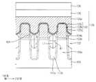
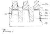
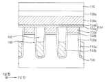
도 1 내지 도 3을 참조하면, 상기 비휘발성 메모리 소자는 제1 방향으로 연장되는 액티브 패턴(100a) 및 상기 액티브 패턴(100a) 사이의 제1 트렌치(108)를 포함하는 기판(100)과, 상기 제1 트렌치(108) 하부를 부분적으로 채우는 소자 분리막 패턴(112b), 상기 기판(100) 상에 터널 절연막 패턴(102b), 플로팅 게이트 패턴(104b), 유전막 구조물(122) 및 콘트롤 게이트 패턴(126a)을 포함하고 제2 방향으로 연장되는 게이트 구조물(129)이 구비된다. 상기 소자 분리막 패턴(112b) 및 유전막 구조물(122) 사이에 제1 에어 갭(132)이 구비되도록, 상기 유전막 구조물(122)은 상기 소자 분리막 패턴(112b)과 이격되면서 상기 제1 트렌치(108) 상부를 덮는 형상을 가질 수 있다.1 to 3, the nonvolatile memory device includes a
상기 액티브 패턴(100a)과 제1 트렌치(108)가 상기 제1 방향과 수직한 제2 방향으로 반복 배치될 수 있다. 상기 액티브 패턴(100a)은 상대적으로 돌출된 형상을 가질 수 있다.The
예시적인 실시예로, 상기 제1 트렌치(108)의 측벽 및 저면을 따라 컨포멀하게 라이너막(110a)이 구비될 수 있다. 상기 라이너막(110a)은 상기 플로팅 게이트 패턴(104b)의 하부 측벽까지 연장될 수 있다. 상기 라이너막(110a)은 상기 제1 트렌치(108)의 측벽을 보호하기 위하여 제공될 수 있다. 예를들어, 상기 라이너막(110a)은 실리콘 산화물, 실리콘 질화물 또는 실리콘 산 산화물을 포함할 수 있다. 상기 라이너막(110a)은 열산화 공정, 화학 기상 증착 공정 또는 고밀도 플라즈마 화학 기상 증착(HDP-CVD) 공정을 통해 형성될 수 있다. 그러나, 다른 예로 상기 라이너막(110a)은 구비되지 않을 수도 있다.In an exemplary embodiment, a
상기 소자 분리막 패턴(112b)은 상기 라이너막(110a)의 일부 표면 상에 구비될 수 있다. 상기 소자 분리막 패턴(112b)는 상기 트렌치를 부분적으로 채울 수 있다. 상기 소자 분리막 패턴(112b)은 상기 제1 방향으로 연장되는 형상을 가질 수 있다. 상기 소자 분리막 패턴(112b)은 다공성을 갖는 실리콘 산화물을 포함할 수 있다. 예시적인 실시예로, 상기 실리콘 산화물은 스핀온 글라스(SOG, Spin on glass) 물질을 포함할 수 있다. 예를들어, 상기 실리콘 산화물은 HSQ(Hydrogensilsesquioxane) SOG, 실리케이트(silicate) SOG 또는 도핑된 실리케이트(doped silicate)를 포함할 수 있다.The device
상기 제1 에어 갭(132)은 상기 소자 분리막 패턴(112b) 상에 형성될 수 있다. 그러므로, 상기 소자 분리막 패턴(112b)의 상부면은 상기 제1 에어 갭(132)의 하부 형상을 결정할 수 있다. 상기 제1 에어 갭(132)의 일부는 상기 소자 분리막 패턴(112b)의 상부면과 상기 유전막 구조물(122)의 하부면 및 상기 제1 트렌치(108) 측벽의 라이너막(110a)에 의해 정의될 수 있으며, 상기 부위를 제1 부위라고 하면서 설명한다.The
상기 소자 분리막 패턴(112b)의 상부면이 낮아질수록 상기 제1 에어 갭(132)의 용적은 커지게 된다. 상기 액티브 패턴들(100a) 간의 기생 커패시턴스를 감소시키기 위하여, 상기 소자 분리막 패턴(112b)의 상부면은 상기 액티브 패턴(100a)의 상부면보다 낮게 위치할 수 있다. 예시적인 실시예에서, 상기 소자 분리막 패턴(112b)의 상부면은 상기 액티브 패턴(100a)의 높이의 70% 보다 낮게 위치할 수 있다.As the upper surface of the device
상기 소자 분리막 패턴(112b)의 상부면은 상기 제 1방향의 단면으로보았을 때 굴곡을 가질 수 있다. 상기 소자 분리막 패턴(112b)의 상부면은 상기 게이트 구조물(122)의 하부면의 제1 방향의 중심 부위와 대향하는 부위에서 상대적으로 돌출되는 형상을 가질 수 있다. 이에 따라, 상기 제1 에어 갭(132)의 하부면은 상기 제 1방향을 따라 굴곡을 가질 수 있고, 상기 게이트 구조물(122)의 하부면의 제1 방향의 중심 부위와 대향하는 부위에서 상기 기판(100) 표면으로부터 수직한 제3 방향으로 더 긴 형상을 가질 수 있다.The upper surface of the device
또한, 상기 소자 분리막 패턴(112b)의 상부면은 상기 제2 방향의 단면으로 보았을 때 하부로 볼록한 형상을 가질 수 있다.In addition, the upper surface of the device
상기 터널 절연막 패턴(102b)은 상기 액티브 패턴(100a) 상에 고립된 형상을 가지면서 형성될 수 있다. 그러므로, 상기 터널 절연막 패턴(102b)은 상기 액티브 패턴(100a) 상에서 상기 제1 방향을 따라 복수개가 형성될 수 있다. 상기 터널 절연막 패턴(102b)은 실리콘 산화물을 포함할 수 있다. 상기 터널 절연막 패턴(102b)은 후속 공정들을 진행할 때 식각되거나 특성이 변하지 않는 것이 바람직하다. 그러므로, 상기 터널 절연막 패턴(102b)에 포함되는 실리콘 산화물은 결정 결함이나 기공이 거의 없는 것이 바람직하다. 예시적인 실시예에서, 상기 터널 절연막 패턴(102b)은 열산화 공정, 화학 기상 증착 공정 또는 HDP-CVD 공정을 통해 형성될 수 있다.The tunnel insulating
상기 플로팅 게이트 패턴(104b)은 상기 터널 절연막 패턴(102b) 상에 적층되고, 고립된 형상을 가질 수 있다. 따라서, 상기 제1 및 제2 방향들을 따라 각각 복수개로 형성될 수 있다. 예시적인 실시예들에 따르면, 플로팅 게이트 패턴(104b)은 불순물, 예를 들어, 인 혹은 비소가 도핑된 폴리실리콘을 포함할 수 있다.The floating
본 발명의 다른 실시예로, 상기 플로팅 게이트 패턴 대신 전하 트랩핑 패턴을 사용할 수도 있다. 이 경우, 상기 전하 트랩핑 패턴은 실리콘 질화물을 포함할 수 있다.In another embodiment of the present invention, the charge trapping pattern may be used in place of the floating gate pattern. In this case, the charge-trapping pattern may comprise silicon nitride.
상기 유전막 구조물(122)은 상기 플로팅 게이트 패턴(104b)의 상부 표면 및 상기 소자 분리막 패턴(112b)과 이격되면서 상기 소자 분리막 패턴(112b) 위에 형성될 수 있다. 상기 유전막 구조물(122)은 상기 제2 방향을 따라 연장되도록 형성되며, 상기 제1 방향을 따라 복수 개로 형성될 수 있다.The
상기 유전막 구조물(122)은 실리콘 산화물 및 실리콘 질화물을 포함할 수 있다. 예시적인 실시예들에 따르면, 유전막 구조물(122)은 실리콘 산화막 패턴(122a)/실리콘 질화막 패턴(122b)/실리콘 산화막 패턴(122c)의 다층막 구조를 가질 수 있다. 이 때, 상기 유전막 구조물에 포함되는 실리콘 산화막 패턴(122a, 122c)은 후속 공정들을 진행할 때 식각되거나 특성이 변하지 않는 것이 바람직하다. 그러므로, 상기 실리콘 산화막 패턴(122a, 122c)은 결정 결함이나 기공이 거의 없는 것이 바람직하다. 예시적인 실시예에서, 상기 실리콘 산화막 패턴(122a, 122c)은 화학 기상 증착 공정 또는 HDP-CVD 공정을 통해 형성된 실리콘 산화물을 포함할 수 있다.The
이와는 다른 예로, 상기 유전막 구조물(122)은 커패시턴스를 증가시키고 누설 전류 특성을 개선하기 위해 고유전율을 갖는 금속 산화물을 포함할 수도 있다. 상기 고유전율을 갖는 금속 산화물로서는 하프늄 산화물, 티타늄 산화물, 탄탈륨 산화물, 지르코늄 산화물, 알루미늄 산화물 등을 들 수 있다.As another example, the
상기 트렌치 상에 위치하는 상기 유전막 구조물(122)의 저면은 상기 제2 방향의 단면으로 보았을 때 하부로 볼록한 형상을 가질 수 있다.The bottom surface of the
상기 유전막 구조물(122) 하부면에는 소자 분리막 패턴(112b)과 동일한 물질의 절연막 패턴(101)이 구비될 수 있다. 상기 절연막 패턴(101)의 하부면 형상에 의해, 상기 제1 에어 갭(132)의 상부면이 정의될 수 있다.An
상기 제1 에어 갭(132)은 상기 제1 부위에서, 상기 제3 방향으로의 w제1 길이(L1)가 상기 제2 방향으로의 제1 폭(W1)보다 더 큰 형상을 가질 수 있다. 예를들어, 상기 제1 에어 갭(132)은 상기 제1 부위에서, 상기 제1 길이(L1)는 상기 제1 폭(W1)의 1.5배 내지 6배일 수 있다.The
상기 제1 에어 갭(132)의 상기 제1 부위에서, 상기 제1 에어 갭(132)의 상부면은 상기 액티브 패턴(100a) 상부면보다 높게 위치할 수 있다. 또한, 상기 제1 부위에서 상기 액티브 패턴(100a) 상부면보다 낮게 위치하는 부위의 제3 방향의 제2 길이(L2)는 상기 액티브 패턴 상부면보다 높게 위치하는 부위의 제3 방향의 제3 길이(L3)의 1.5배 내지 5배일 수 있다.In the first portion of the
상기 제1 에어 갭(132)의 상기 제1 부위에서, 상기 제1 에어 갭의 상, 하부는 라운드 형상을 가질 수 있다. 또한, 상기 제1 에어 갭(132)의 상기 제1 부위에서, 상기 제2 방향으로 절단한 단면은 하방으로 긴 타원 형상을 가질 수 있다.In the first portion of the
상기 콘트롤 게이트 패턴(126a)은 유전막 구조물(122) 상에 구비된다. 상기 콘트롤 게이트 패턴(126a)은 상기 제2 방향으로 연장되는 라인 형상을 가질 수 있으며, 상기 제1 방향을 따라 복수 개로 형성될 수 있다. 상기 콘트롤 게이트 패턴(126a)은 워드 라인의 기능을 할 수 있다. 상기 콘트롤 게이트 패턴(126a)은 불순물이 도핑된 폴리실리콘 및/또는 금속을 포함할 수 있다. 예를들어, 상기 콘트롤 게이트 패턴(126a)은 폴리실리콘 패턴 및 금속 패턴이 적층된 형상을 가질 수 있다.The
상기 콘트롤 게이트 패턴(126a) 상에는 하드 마스크(128)가 구비될 수 있다. 상기 하드 마스크(128)는 실리콘 질화물 또는 실리콘 산 질화물을 포함할 수 있다.A
도시하지는 않았지만, 상기 터널 절연막 패턴(102b), 플로팅 게이트 패턴(104b), 유전막 구조물(122), 콘트롤 게이트 패턴(126a) 및 하드 마스크(128)를 포함하는 상기 게이트 구조물(129)의 측벽에는 스페이서가 더 구비될 수도 있다. 상기 스페이서는 실리콘 질화물 또는 실리콘 산 질화물을 포함할 수 있다.Although not shown, on the side wall of the
상기 게이트 구조물들(129) 사이에는 층간 절연막(136)이 구비될 수 있다. 상기 층간 절연막(136)은 실리콘 산화물을 포함할 수 있다.An interlayer insulating
상기 층간 절연막(136)은 상기 제1 에어 갭(132) 내부를 채우지 않고, 상기 게이트 구조물들(129) 사이의 갭의 상부를 부분적으로 채우는 형상을 가질 수 있다.The interlayer insulating
그러므로, 상기 층간 절연막(136)은 상기 소자 분리막 패턴(112b)의 상부면과 이격되도록 형성될 수 있다. 예시적인 실시예에서, 상기 층간 절연막은 상기 콘트롤 게이트 패턴들(126a) 사이에 제2 에어 갭이 생성되도록 상기 하드 마스크들(128) 사이의 갭 부위를 채우는 형상을 가질 수 있다. 즉, 상기 층간 절연막(136)의 저면은 상기 콘트롤 게이트 패턴(126a)의 최하부면보다 높게 위치하도록 형성될 수 있다. 따라서, 상기 제2 에어 갭(130a)은 상기 제2 방향으로 연장되는 형상을 가질 수 있다.Therefore, the
상기 제1 및 제2 에어 갭(132, 130a)은 서로 연통하는 형상을 가질 수 있으며, 서로 교차하도록 배치될 수 있다.
The first and
도 4 내지 도 8은 도 1 내지 도 3에 도시된 비휘발성 메모리 소자의 제조 방법을 설명하기 위한 단면도들이고, 도 9 내지 도 12는 상기 비휘발성 메모리 소자의 제조 방법을 설명하기 위한 사시도들이다.FIGS. 4 to 8 are sectional views for explaining a method of manufacturing the nonvolatile memory device shown in FIGS. 1 to 3, and FIGS. 9 to 12 are perspective views for explaining a method of manufacturing the nonvolatile memory device.
도 4를 참조하면, 기판(100) 상에 터널 절연막(102), 플로팅 게이트막(104)을 순차적으로 형성하고, 상기 플로팅 게이트막(104) 상에 제1 마스크(106)를 순차적으로 형성한다.4, a
상기 기판(100)은 실리콘 기판, 게르마늄 기판, 실리콘-게르마늄 기판, 실리콘-온-인슐레이터(Silicon-On-Insulator: SOI) 기판, 게르마늄-온-인슐레이터(Germanium-On-Insulator: GOI) 기판 등의 반도체 기판을 포함할 수 있다.The
상기 터널 절연막(102)은 실리콘 산화물을 증착하여 형성할 수 있다.상기 터널 절연막(102)에 포함되는 실리콘 산화물은 결정 결함이나 기공이 거의 없는 것이 바람직하다. 예시적인 실시예에서, 상기 터널 절연막(102)은 열산화 공정, 화학 기상 증착 공정 또는 HDP-CVD 공정을 통해 형성될 수 있다.The
상기 플로팅 게이트막(104)은 불순물이 도핑된 폴리실리콘을 사용하여 형성할 수 있다. 일 실시예에 따르면, 플로팅 게이트막(104)은 저압 화학 기상 증착 공정을 통해 형성될 수 있다.The floating
상기 제1 마스크(106)는 포토레지스트 패턴 또는 하드 마스크일 수 있다. 예시적인 실시예들에 따르면, 제1 마스크(106)는 제1 방향으로 연장되는 라인 형상을 갖도록 형성된다.The
도 5를 참조하면, 제1 마스크(106)를 식각 마스크로 사용하여 플로팅 게이트막(104), 터널 절연막(102) 및 기판(100) 상부를 순차적으로 식각한다. 이에 따라, 상기 기판에는 제1 방향으로 연장되는 액티브 패턴들(100a)이 형성된다. 상기 액티브 패턴들(100a) 상에는 예비 터널 절연막 패턴(102a) 및 예비 플로팅 게이트 패턴(104a)이 형성된다. 또한, 상기 예비 터널 절연막 패턴(102a) 및 예비 플로팅 게이트 패턴(104a) 및 액티브 패턴들 사이에는 제1 트렌치(108)가 형성된다.Referring to FIG. 5, the floating
상기 예비 플로팅 게이트 패턴(104a) 및 예비 터널 절연막 패턴(102a)은 상기 제1 방향으로 연장되는 라인 형상을 가질 수 있으며, 상기 제1 방향에 실질적으로 수직한 제2 방향으로 일정 간격으로 이격되면서 복수 개로 형성될 수 있다.The preliminary floating
도 6을 참조하면, 상기 제1 트렌치(108) 내벽, 상기 예비 터널 절연막 패턴(102a) 및 예비 플로팅 게이트 패턴(104a)의 표면 상에 컨포멀하게 예비 라이너막(110)을 형성한다.Referring to FIG. 6, a
예시적인 실시예들에 따르면, 상기 예비 라이너막(110)은 실리콘 산화물, 실리콘 질화물 또는 실리콘 산 질화물을 사용하여 형성할 수 있다. 상기 예비 라이너막(110)은 화학 기상 증착공정 또는 원자층 적층 공정을 통해 형성할 수 있다. 그러나, 다른 예로 상기 예비 라이너막은 형성하지 않을 수도 있다.According to exemplary embodiments, the
상기 예비 라이너막(110) 상에 상기 제1 트렌치(108) 내부를 채우는 제1 예비 소자 분리막 패턴(112)을 형성한다.A first preliminary element
구체적으로, 상기 제1 트렌치(108) 내부를 완전하게 채우도록 소자 분리막을 형성한다. 상기 소자 분리막은 다공성을 갖는 실리콘 산화물을 포함할 수 있다. 예시적인 실시예로, 상기 실리콘 산화물은 스핀온 글라스(SOG, Spin on glass) 물질을 포함할 수 있다. 예를들어, 상기 실리콘 산화물은 HSQ(Hydrogensilsesquioxane) SOG, 실리케이트(silicate) SOG 또는 도핑된 실리케이트(doped silicate)를 포함할 수 있다. 상기 제1 마스크(106)의 상부면이 노출되도록 상기 소자 분리막을 평탄화하여 상기 제1 예비 소자 분리막 패턴(112)을 형성한다. 상기 평탄화는 에치백 또는 화학기계적 연마를 포함할 수 있다.Specifically, an element isolation film is formed so as to completely fill the inside of the
도 7을 참조하면, 제1 예비 소자 분리막 패턴(112) 및 상기 예비 라이너막(110)의 상부를 부분적으로 식각하여 제2 예비 소자 분리막 패턴(112a) 및 라이너막(110)을 형성한다. 상기 식각 공정은 에치 백(etch-back) 공정을 포함할 수 있다. 상기 식각 공정에 의해, 상기 예비 플로팅 게이트 패턴(104a)의 상부 측벽이 노출될 수 있다. 상기 식각 공정을 수행한 다음, 상기 제1 마스크(106)는 제거될 수 있다.Referring to FIG. 7, the first preliminary element
상기 제2 예비 소자 분리막 패턴(112a)의 상부면은 상기 예비 터널 절연막 패턴(102a)의 상부면보다 높게 형성될 수 있다.The upper surface of the second preliminary element
후속 공정에서, 상기 제2 예비 소자 분리막 패턴(112a) 상에 유전막 구조물이 형성될 수 있다. 그러므로, 상기 유전막 구조물의 하부면은 상기 제2 예비 소자 분리막 패턴(112a)이 상부면 위치 및 형상과 동일할 수 있다. 예시적인 실시예에서, 상기 제2 예비 소자 분리막 패턴(112a)은 상부면은 상기 제2 방향으로 절단한 단면에서 볼 때 라운드될 수 있으며, 하방으로 볼록할 수 있다.In a subsequent process, a dielectric film structure may be formed on the second preliminary element
도 8 및 9를 참조하면, 노출된 상기 예비 플로팅 게이트 패턴(104a) 및 제2 예비 소자 분리막 패턴(112a)의 상부면을 따라 예비 유전막 구조물(120)을 형성한다. 상기 예비 유전막 구조물(120) 상에는 콘트롤 게이트막(126) 및 하드 마스크막(127)을 형성한다.Referring to FIGS. 8 and 9, a preliminary
상기 예비 유전막 구조물(120)은 실리콘 산화물 및 실리콘 질화물을 사용하여 형성될 수 있다. 예시적인 실시예들에 따르면, 상기 예비 유전막 구조물(120)은 실리콘 산화막(120a)/실리콘 질화막(120b)/실리콘 산화막(120c)의 구조를 갖도록 형성될 수 있다. 상기 예비 유전막 구조물(120)에 포함되는 상기 실리콘 산화막(120a, 120c)은 화학 기상 증착 공정 또는 HDP-CVD 공정을 통해 형성될 수 있다.The
이와는 다른 실시예로, 상기 예비 유전막 구조물(120)은 고유전율을 갖는 금속 산화물을 사용하여 형성할 수 있다. 상기 고유전율을 갖는 금속 산화물의 예로는 하프늄 산화물, 티타늄 산화물, 탄탈륨 산화물, 지르코늄 산화물, 알루미늄 산화물 등을 들 수 있다.In another embodiment, the
상기 콘트롤 게이트막(126)은 불순물이 도핑된 폴리실리콘, 금속, 금속 질화물, 금속 실리사이드 등을 사용하여 형성할 수 있다. 예시적인 실시예에서, 상기 콘트롤 게이트막(126)은 불순물이 도핑된 폴리실리콘막 및 텅스텐막을 차례로 증착시켜 형성할 수 있다.The
상기 콘트롤 게이트막(126) 상에 하드 마스크막(127)을 형성한다. 상기 하드 마스크막은 예를들어, 실리콘 질화물 또는 실리콘 산 질화물을 사용하여 형성할 수 있다.A
도 10을 참조하면, 상기 하드 마스크막(127)을 패터닝하여 상기 하드 마스크(128)를 형성한다. 상기 하드 마스크(128)는 제2 방향으로 연장되는 라인 형상을 가질 수 있다. 상기 하드 마스크(128)는 예를들어, 실리콘 질화물 또는 실리콘 산 질화물을 포함할 수 있다.Referring to FIG. 10, the
상기 하드 마스크(128)를 식각 마스크로 사용하여, 상기 콘트롤 게이트막(126), 예비 유전막 구조물(120), 예비 플로팅 게이트 패턴(104a) 및 예비 터널 절연막 패턴(102a)을 이방성 식각한다. 이에 따라, 기판(100) 상에 순차적으로 적층된 터널 절연막 패턴(102b), 플로팅 게이트 패턴(104b), 유전막 구조물(122), 콘트롤 게이트 패턴(126a) 및 하드 마스크(128)를 포함하는 게이트 구조물들(129)이 형성된다. 또한, 상기 게이트 구조물들(129) 사이에는 제2 트렌치(130)가 형성될 수 있다. 상기 식각 공정에서, 상기 제2 예비 소자 분리막 패턴(112a)의 상부면이 일부 식각될 수 있다.The
예시적인 실시예들에 따르면, 상기 터널 절연막 패턴(102b) 및 플로팅 게이트 패턴(104b)은 기판(100)의 상기 액티브 패턴(100a) 상에 고립된 형상으로 형성될 수 있다. 또한, 상기 유전막 구조물(122) 및 콘트롤 게이트 패턴(126a)은 각각 상기 제2 방향으로 연장되도록 형성될 수 있다. 이에 따라, 콘트롤 게이트 패턴(126a)은 워드 라인의 기능을 할 수 있다.According to exemplary embodiments, the tunnel insulating
도시하지는 않았지만, 상기 게이트 구조물들(129) 양 측에 스페이서를 형성할 수도 있다. 상기 스페이서는 실리콘 질화물 또는 실리콘 산 질화물을 사용하여 형성할 수 있다. 그러나, 상기 게이트 구조물들 사이의 기생커패시터 감소들 위하여, 상기 스페이서는 형성되지 않을 수도 있다.Although not shown, spacers may be formed on both sides of the
도 11을 참조하면, 상기 제2 트렌치(130) 저면에 노출되는 상기 제2 예비 소자 분리막 패턴(112a)을 등방성 건식 식각을 통해 일부 제거하여 소자 분리막 패턴(112b)을 형성한다. 이에 따라, 상기 소자 분리막 패턴(112b) 상에는 제1 에어 갭(132)이 형성된다. 상기 등방성 건식 식각은 가스상 식각(gas phase etching) 공정으로 수행될 수 있다. 예를들어, 상기 등방성 건식 식각은 건식 세정 공정 설비에서 수행될 수 있다.Referring to FIG. 11, the second preliminary element
상기 제2 예비 소자 분리막 패턴(112a)을 식각할 때, 산화물을 포함하는 터널 절연막 패턴(102b) 및 유전막 구조물(122)은 거의 식각되지 않도록 하여야 한다. 즉, 상기 제2 예비 소자 분리막 패턴(112a)은 상기 터널 절연막 패턴(102b) 및 유전막 구조물(122)보다 상대적으로 빠르게 식각되어야 한다. 이를 위하여, 상기 등방성 건식 식각은 불소를 포함하는 가스 및 기상 상태의 H2O를 함께 식각 가스로 사용할 수 있다. 상기 불소를 포함하는 가스의 예로는 CxFy, CHxFy 등을 들 수 있다.When the second preliminary element
구체적으로, 상기 제2 예비 소자 분리막 패턴(112a)에 상기 기상 상태의 H2O를 선택적으로 흡습시킨다. 상기 제2 예비 소자 분리막 패턴(112a)은 다공성의 실리콘 산화물을 포함하며, 결정 결함이나 댕글링 본드가 상기 터널 절연막 패턴(102b) 및 유전막 구조물(122)의 산화물에 비해 더 많다. 그러므로, 상기 제2 예비 소자 분리막 패턴(112a)의 표면에는 기상 상태의 H2O가 용이하게 흡습될 수 있다. 반면에, 상기 터널 절연막 패턴(102b) 및 유전막 구조물(122a)은 상기 기상 상태의 H2O가 표면에 거의 흡습되지 않을 수 있다.Specifically, H2 O in the gaseous state is selectively absorbed in the second preliminary element
상기 제2 예비 소자 분리막 패턴(112a)이 흡습된 상태에서는 상기 실리콘과 산소의 결합이 실리콘과 불소의 결합으로 빠르게 치환될 수 있다. 즉, 상기 불소를 포함하는 가스를 이용하여 상기 흡습된 제2 예비 소자 분리막 패턴(112a)이 빠르게 식각될 수 있다. 상기 기상 상태의 H2O가 빠르게 흡습될 수 있도록 상기 등방성 건식 식각은 5 내지 50도의 온도에서 수행할 수 있다.In the state where the second preliminary element
한편, 상기 터널 절연막 패턴(102b) 및 유전막 구조물(122a)은 상기 기상 상태의 H2O가 표면에 거의 흡습되지 않기 때문에, 상기 실리콘과 산소의 결합이 실리콘과 불소의 결합으로 치환되기가 어렵다. 때문에, 상기 터널 절연막 패턴(102b) 및 유전막 구조물(122)은 상기 불소를 포함하는 가스에 의해 식각되지 않을 수 있다.On the other hand, since the gas phase H2 O is hardly absorbed on the surface of the tunnel insulating
상기 등방성 건식 식각에서, 터널 절연막 패턴(102b) 및 유전막 구조물의 산화막 패턴들(122a, 122c)의 식각 속도 : 상기 제2 예비 소자 분리막 패턴(112a)의 식각 속도는 1 : 50 내지 300일 수 있다.In the isotropic dry etching, the etching rate of the tunnel insulating
따라서, 상기 제2 예비 소자 분리막 패턴(112a)의 일부를 식각하는 공정에서 상기 터널 절연막 패턴(102b) 및 유전막 구조물(122)의 손상이나 식각되지 않으므로, 비휘발성 메모리 소자는 원하는 전기적 특성을 가질 수 있다.Accordingly, in the step of etching a part of the second preliminary element
일반적으로, 상기 제2 예비 소자 분리막 패턴(112a)을 불산을 이용하는 습식 식각 공정을 사용하여 식각하는 경우에는, 상기 터널 절연막 패턴(102b) 및 유전막 구조물(122)에 포함되는 산화막 패턴(122a, 122c)과 상기 제2 예비 소자 분리막 패턴(112a)의 식각 속도비가 1: 1.5 내지 5 정도로 낮다. 때문에, 상기 식각 공정에서, 상기 터널 절연막 패턴(102b) 및 유전막 구조물(122)도 일부 식각될 수 있다. 따라서, 비휘발성 메모리 소자는 원하는 전기적 특성을 확보하기가 어려울 수 있다.In general, when the second preliminary
상기 등방성 건식 식각하면, 상기 제2 예비 소자 분리막 패턴(112a)의 노출된 상부 표면으로부터 식각이 이루어지므로, 상기 제1 에어 갭(132)은 상기 제1 방향으로 연장될 수 있다.When the isotropic dry etching is performed, the
또한, 상기 게이트 구조물들(122) 사이로부터 상기 제1 방향을 따라 상기 제2 예비 소자 분리막 패턴(112a)의 표면 부위가 식각된다. 때문에, 상기 게이트 구조물(122)의 제1 방향 중심부와 대향하는 부위의 제2 예비 소자 분리막 패턴(112a)은 상기 게이트 구조물들(122) 사이 부위의 제2 예비 소자 분리막 패턴(112a)보다 식각되는 양이 더 작게 될 수 있다. 따라서, 상기 소자 분리막 패턴(112b)의 상부면은 상기 제1 방향의 단면으로 보았을 때 굴곡된 형상을 가질 수 있다. 즉, 상기 게이트 구조물(122)의 제1 방향 중심부와 대향하는 부위의 소자 분리막 패턴(112b)의 상부면은 상대적으로 더 높게 돌출될 수 있다. 또한, 상기 제1 에어 갭(132)의 하부면은 상기 게이트 구조물(122)의 제1 방향 중심부와 대향하는 부위의 소자 분리막 패턴(112b)의 상부면은 상대적으로 더 낮게 위치할 수 있다.In addition, the surface portions of the second preliminary element
상기 소자 분리막 패턴(112b)의 상부면이 낮아질수록 상기 제1 에어 갭(132)의 용적은 커지게 된다. 상기 액티브 패턴들(100a) 간의 기생 커패시턴스를 감소시키기 위하여, 상기 소자 분리막 패턴(112b)의 상부면은 상기 액티브 패턴(100a)의 상부면보다 낮게 되도록 할 수 있다. 바람직하게는, 상기 소자 분리막 패턴(112b)의 상부면은 상기 액티브 패턴(100a)의 높이의 70% 보다 낮게 위치할 수 있다.As the upper surface of the device
또한, 상기 소자 분리막 패턴(112b)과 유전막 구조물(122) 사이에서, 상기 제1 에어 갭(132)의 상부면은 상기 액티브 패턴(100a) 상부면보다 높게 위치할 수 있다. 상기 제1 에어 갭(132)에서 상기 액티브 패턴(100a) 상부면보다 낮게 위치하는 부위의 제3 방향의 제2 길이는 상기 액티브 패턴 상부면보다 높게 위치하는 부위의 제3 방향의 제3 길이의 1.5배 내지 5배가 되도록 할 수 있다.The upper surface of the
상기 등방성 식각 공정에서 상기 라이너막(110a)이 노출될 수 있으며, 상기 라이너막(110a)은 식각되지 않는다. 그러므로, 상기 제1 에어 갭(132)의 제2 방향으로의 폭은 상기 라이너막(110a) 사이의 제1 트렌치(108)의 폭으로 한정될 수 있다. 상기 제1 에어 갭(132)은 상기 제2 방향의 제1 폭보다 상기 기판 표면으로부터 수직한 방향인 제3 방향으로의 제1 길이가 더 긴 형상을 갖도록 형성될 수 있다. 예를들어, 상기 제1 에어 갭(132)의 상기 제1 길이는 상기 제1 폭의 1.5배 내지 6배가 되도록 형성할 수 있다.In the isotropic etching process, the
일 실시예에서, 상기 유전막 구조물(122)의 저면에 상기 제2 예비 소자 분리막 패턴(112a)이 일부 남아서 절연막 패턴(101)이 형성될 수 있다. 이 경우, 상기 절연막 패턴(101)에 의해 상기 제1 에어 갭(132)의 상부면이 정의될 수 있다. 본 실시예에서, 상기 소자 분리막 패턴(112b)과 유전막 구조물(122) 사이에서, 상기 제1 에어 갭(132)의 상, 하부는 라운드 형상을 가질 수 있다. 따라서, 상기 제1 에어 갭에서 상기 제2 방향의 단면은 하방으로 긴 타원 형상을 가질 수 있다.In one embodiment, a portion of the second preliminary element
도 12를 참조하면, 상기 콘트롤 게이트 패턴(126a) 사이의 제2 트렌치(130)의 상부를 부분적으로 채우는 층간 절연막(136)을 형성한다.Referring to FIG. 12, an
구체적으로, 플라즈마 증대 산화물(PEOX) 혹은 중온 산화물(MTO) 등과 같은 실리콘 산화물을 사용하여 낮은 스텝 커버리지 특성을 갖는 공정을 수행함으로써 상기 층간 절연막(136)을 형성한다. 예시적인 실시예에서, 상기 층간 절연막(136)의 하부는 상기 콘트롤 게이트 패턴(126a) 최하부면보다 높게 위치하도록 할 수 있다. 따라서, 상기 콘트롤 게이트 패턴(126a) 사이에는 상기 제1 에어 갭(132)과 연통하는 제2 에어 갭(130a)이 형성될 수 있다.Specifically, the
상기 제2 에어 갭(130a)은 상기 제2 방향으로 연장되는 에어 터널 형상을 가질 수 있다. 상기 제2 에어 갭(130a)이 구비됨으로써, 상기 콘트롤 게이트 패턴(126a) 간의 기생 커패시턴스가 감소될 수 있다.The
이후, 공통 소스 라인(도시되지 않음), 비트 라인(도시되지 않음) 등의 배선들을 형성함으로써 상기 비휘발성 메모리 소자를 완성할 수 있다.
Thereafter, the nonvolatile memory element can be completed by forming wirings such as a common source line (not shown), a bit line (not shown) and the like.
실시예 2Example 2
도 13은 본 발명의 실시예 2에 따른 비휘발성 메모리 소자를 설명하기 위한 사시도이다. 상기 비휘발성 메모리 소자는 제1 에어 갭의 형상 및 유전막 구조물 하부의 절연막 패턴을 제외하고는 실시예 1의 비휘발성 메모리 소자와 실질적으로 동일하다. 이에 따라, 동일한 구성 요소에는 동일한 참조 부호를 부여하고 이에 대한 자세한 설명은 생략한다.13 is a perspective view illustrating a nonvolatile memory device according to a second embodiment of the present invention. The nonvolatile memory element is substantially the same as the nonvolatile memory element of the first embodiment except for the shape of the first air gap and the insulating film pattern under the dielectric film structure. Accordingly, the same components are denoted by the same reference numerals, and a detailed description thereof will be omitted.
도 13을 참조하면, 상기 유전막 구조물(122) 하부면에 절연막 패턴이 구비되지 않는다. 따라서, 상기 제1 에어 갭(132a)의 제1 부위에서, 상기 제1 에어 갭(132a)의 상부면은 상기 유전막 구조물(122)의 하부면에 의해 정의될 수 있다.Referring to FIG. 13, an insulating film pattern is not provided on the lower surface of the
따라서, 상기 제1 에어갭(132a)의 상부면은 라운드되고, 상기 제2 방향의 단면에서 보았을 때 하방으로 볼록한 형상을 가질 수 있다.Accordingly, the upper surface of the
도 14는 도 13에 도시된 비휘발성 메모리 소자의 제조 방법을 설명하기 위한 사시도이다.14 is a perspective view for explaining a method of manufacturing the nonvolatile memory device shown in FIG.
상기 비휘발성 메모리 소자는 실시예 1의 비휘발성 메모리 소자의 제조 방법과 매우 유사한 방법에 의해 제조될 수 있다.The nonvolatile memory element can be manufactured by a method very similar to the method of manufacturing the nonvolatile memory element of
즉, 도 4 내지 도 10을 참조로 설명한 공정과 실질적으로 동일한 공정들을 수행한다.That is, the processes substantially the same as those described with reference to Figs. 4 to 10 are performed.
도 14를 참조하면, 상기 유전막 구조물(122) 아래에 상기 제2 예비 소자 분리막 패턴(112a)이 완전하게 제거되도록 상기 제2 예비 소자 분리막 패턴(112a)를 등방성 건식 식각한다. 상기 등방성 건식 식각 공정 조건은 도 11을 참조로 설명한 것과 실질적으로 동일할 수 있다.Referring to FIG. 14, the second preliminary element
따라서, 상기 제1 부위에서, 하방으로 볼록하게 라운드된 형상을 갖는 제1 에어 갭(132a)을 형성할 수 있다.Accordingly, the
이 후, 도 12를 참조로 설명한 공정을 동일하게 수행하여, 도 13에 도시된 비휘발성 메모리 소자를 제조할 수 있다.
Thereafter, the nonvolatile memory device shown in FIG. 13 can be manufactured by performing the same process as described with reference to FIG.
실시예 3Example 3
도 15는 본 발명의 실시예 3에 따른 비휘발성 메모리 소자를 설명하기 위한 사시도이다. 상기 비휘발성 메모리 소자는 제1 에어 갭 및 지지막 패턴을 제외하고는 실시예 1의 비휘발성 메모리 소자와 실질적으로 동일하다. 이에 따라, 동일한 구성 요소에는 동일한 참조 부호를 부여하고 이에 대한 자세한 설명은 생략한다.15 is a perspective view for explaining a nonvolatile memory device according to a third embodiment of the present invention. The nonvolatile memory element is substantially the same as the nonvolatile memory element of the first embodiment except for the first air gap and the supporting film pattern. Accordingly, the same components are denoted by the same reference numerals, and a detailed description thereof will be omitted.
도 15를 참조하면, 상기 소자 분리막 패턴(112b) 상에 상기 유전막 구조물(122)을 지지하는 지지막 패턴(140)이 구비된다. 상기 지지막 패턴(140)은 상기 소자 분리막 패턴(112b)과 실질적으로 동일한 물질을 포함할 수 있다.Referring to FIG. 15, a
상기 지지막 패턴(140)은 상기 유전막 구조물(122)의 저면의 적어도 일부를 지지하는 형상을 가질 수 있다. 즉, 상기 지지막 패턴(140)의 제1 방향의 최소 폭은 상기 유전막 구조물(122)의 저면의 제1 방향의 폭보다 작을 수 있다. 상기 지지막 패턴(140)이 구비됨에 따라, 제1 에어 갭(132b)의 격벽으로 제공될 수 있다. 따라서, 상기 제1 에어 갭(132b)은 상기 지지막 패턴(140)에 의해 공간이 한정될 수 있다.The
한편, 상기 비휘발성 메모리 소자는 실시예 1의 비휘발성 메모리 소자의 제조 방법과 매우 유사한 방법에 의해 제조될 수 있다.On the other hand, the non-volatile memory device can be manufactured by a method very similar to that of the non-volatile memory device of the first embodiment.
즉, 도 4 내지 도 10을 참조로 설명한 공정과 실질적으로 동일한 공정들을 수행한다. 다음에, 상기 유전막 구조물(122) 아래에서 상기 제2 예비 소자 분리막 패턴(112a)이 제1 방향으로 서로 관통하지 않도록 하면서 상기 제2 예비 소자 분리막 패턴(112a)를 등방성 건식 식각한다. 상기 등방성 건식 식각 공정 조건은 도 11을 참조로 설명한 것과 실질적으로 동일할 수 있다.That is, the processes substantially the same as those described with reference to Figs. 4 to 10 are performed. Next, the second preliminary element
상기 등방성 건식 식각 공정을 수행하면, 상기 제1 트렌치(108) 하부에는 소자 분리막 패턴(112b)이 형성되고, 상기 소자 분리막 패턴(112b) 상에는 상기 유전막 구조물(122)을 지지하는 지지막 패턴(140)이 형성될 수 있다.A device
이 후, 도 12를 참조로 설명한 공정을 동일하게 수행하여, 도 15에 도시된 비휘발성 메모리 소자를 제조할 수 있다.
Thereafter, the nonvolatile memory device shown in FIG. 15 can be manufactured by performing the same process as described with reference to FIG.
실시예 4Example 4
도 16은 본 발명의 실시예 4에 따른 비휘발성 메모리 소자를 설명하기 위한 사시도이다. 상기 비휘발성 메모리 소자는 제2 에어 갭이 구비되지 않는 것을 제외하고는 실시예 1의 비휘발성 메모리 소자와 실질적으로 동일하다. 이에 따라, 동일한 구성 요소에는 동일한 참조 부호를 부여하고 이에 대한 자세한 설명은 생략한다.16 is a perspective view for explaining a nonvolatile memory device according to a fourth embodiment of the present invention. The non-volatile memory device is substantially the same as the non-volatile memory device of the first embodiment except that the second air gap is not provided. Accordingly, the same components are denoted by the same reference numerals, and a detailed description thereof will be omitted.
도 16을 참조하면, 상기 게이트 구조물들(129) 사이를 채우는 층간 절연막(136a)이 구비된다. 다만, 상기 층간 절연막(136a)의 저면은 상기 플로팅 게이트 패턴(104b)의 저면보다 높게 구비되어, 제1 에어 갭(132)이 제1 방향으로 연장될 수 있다.Referring to FIG. 16, an
한편, 상기 비휘발성 메모리 소자는 실시예 1의 비휘발성 메모리 소자의 제조 방법과 매우 유사한 방법에 의해 제조될 수 있다.On the other hand, the non-volatile memory device can be manufactured by a method very similar to that of the non-volatile memory device of the first embodiment.
즉, 도 4 내지 도 11을 참조로 설명한 공정과 실질적으로 동일한 공정들을 수행한 후, 상기 게이트 구조물들(129) 사이에 층간 절연막(136a)을 형성한다. 이때, 상기 층간 절연막136a)의 저면이 상기 플로팅 게이트 패턴104b)의 저면보다 높게 위치하도록 형성함으로써, 상기 비휘발성 메모리 소자를 제조할 수 있다.
That is, after performing the processes substantially the same as those described with reference to FIGS. 4 to 11, an
실시예 5Example 5
도 17은 본 발명의 실시예 4에 따른 비휘발성 메모리 소자를 설명하기 위한 사시도이다. 상기 비휘발성 메모리 소자는 제2 에어 갭이 구비되지 않는 것과 상기 제1 에어 갭의 형상을 제외하고는 실시예 1의 비휘발성 메모리 소자와 실질적으로 동일하다. 이에 따라, 동일한 구성 요소에는 동일한 참조 부호를 부여하고 이에 대한 자세한 설명은 생략한다.17 is a perspective view for explaining a nonvolatile memory device according to a fourth embodiment of the present invention. The nonvolatile memory element is substantially the same as the nonvolatile memory element of
도 17을 참조하면, 상기 게이트 구조물들(129) 사이를 채우는 층간 절연막(136b)이 구비된다. 다만, 상기 층간 절연막(136b)의 저면은 상기 소자 분리막 패턴(112b) 상부면까지 연장될 수 있다. 그러므로, 상기 층간 절연막(136b)은 제1 에어 갭(132c)의 격벽으로 제공될 수 있다. 상기 제1 에어 갭(132c)은 상기 층간 절연막(136b)에 의해 공간이 한정될 수 있다.Referring to FIG. 17, an
한편, 상기 비휘발성 메모리 소자는 실시예 1의 비휘발성 메모리 소자의 제조 방법과 매우 유사한 방법에 의해 제조될 수 있다.On the other hand, the non-volatile memory device can be manufactured by a method very similar to that of the non-volatile memory device of the first embodiment.
즉, 도 4 내지 도 11을 참조로 설명한 공정과 실질적으로 동일한 공정들을 수행한 후, 상기 게이트 구조물들(129) 사이에 층간 절연막(136b)을 형성한다. 이때, 상기 층간 절연막(136b)의 저면이 상기 소자 분리막 패턴(112b)까지 연장되도록 함으로써, 상기 비휘발성 메모리 소자를 제조할 수 있다.
That is, after performing the processes substantially the same as those described with reference to FIGS. 4 to 11, an
실시예 6Example 6
도 18 및 19는 본 발명의 실시예 6에 따른 비휘발성 메모리 소자를 설명하기 위한 사시도 및 단면도이다. 상기 비휘발성 메모리 소자는 유전막 구조물이 플랫한 구조를 가질 수 있다.18 and 19 are a perspective view and a cross-sectional view for explaining a nonvolatile memory device according to a sixth embodiment of the present invention. The nonvolatile memory device may have a flat structure of the dielectric film structure.
도 18 및 도 19를 참조하면, 기판(100)의 제1 트렌치(108) 하부를 부분적으로 채우는 소자 분리막 패턴(112a)이 구비된다. 상기 제1 트렌치(108)의 측벽 및 저면을 따라 라이너막(110a)이 구비될 수 있다.Referring to FIGS. 18 and 19, a device
터널 절연막 패턴(102b) 상에는 전하 저장막 패턴이 구비된다. 상기 전하 저장막 패턴은 고립된 형상을 가지면서 규칙적으로 배치된다. 상기 전하 저장막 패턴은 플로팅 게이트 패턴 또는 전하 트랩 패턴일 수 있다. 상기 전하 저장막 패턴이 플로팅 게이트 패턴(150a)일 경우, 폴리실리콘을 포함할 수 있다. 또한, 상기 전하 저장막 패턴이 전하 트랩 패턴일 경우, 실리콘 질화물을 포함할 수 있다. 이하에서는, 상기 전하 저장막 패턴이 플로팅 게이트 패턴(150a)인 것으로 설명한다.A charge storage film pattern is provided on the tunnel insulating
상기 플로팅 게이트 패턴(150a)은 상기 터널 절연막 패턴(102b)의 두께의 0.1 내지 10배의 얇은 두께를 가질 수 있다.The floating
상기 플로팅 게이트 패턴(150a) 상에는 유전막 구조물(154)이 구비된다. 상기 유전막 구조물(154)의 하부면은 상기 플로팅 게이트 패턴(150a) 상부면과 접촉하면서 실질적으로 평탄할 수 있다. 상기 유전막 구조물(154)은 상기 제2 방향으로 연장되는 형상을 가질 수 있다.A
예시적인 실시예에서, 상기 유전막 구조물(154)은 실리콘 산화막(154a) 및 실리콘 질화물보다 높은 유전율을 갖는 금속 산화막(154b)이 적층되는 구조를 가질 수 있다. 다른 예로, 상기 유전막 구조물은 실리콘 산화막 패턴 실리콘 질화막 패턴 및 실리콘 산화막 패턴이 적층되는 구조를 가질 수도 있다.In an exemplary embodiment, the
상기 유전막 구조물(154) 상에 콘트롤 게이트 패턴(156a)이 구비될 수 있다. 상기 콘트롤 게이트 패턴(156a)은 상기 제2 방향으로 연장되는 라인 형상을 가질 수 있다. 상기 콘트롤 게이트 패턴(156a)은 상기 플로팅 게이트 패턴(150a)의 측벽 부위와 서로 대향하지 않을 수 있다. 즉, 상기 콘트롤 게이트 패턴(156a)의 저면은 상기 플로팅 게이트 패턴(150a) 상부면보다 높게 위치할 수 있다.A
제1 에어 갭(162)은 상기 소자 분리막 패턴(112b)의 상부면과 상기 유전막 구조물(154)의 하부면 및 상기 제1 트렌치(108) 측벽의 라이너막(110a)에 의해 정의될 수 있다. 상기 소자 분리막 패턴(112b)의 상부면과 상기 유전막 구조물(154)의 하부면 사이의 제1 에어 갭(162)은 실시예 1과 실질적으로 동일한 형상을 가질 수 있다. 다만, 상기 제1 에어 갭(162)은 상기 플로팅 게이트 패턴(150a)의 측벽 전체와 대향할 수 있다.The
한편, 상기 비휘발성 메모리 소자는 실시예 1의 비휘발성 메모리 소자의 제조 방법과 매우 유사한 방법에 의해 제조될 수 있다.On the other hand, the non-volatile memory device can be manufactured by a method very similar to that of the non-volatile memory device of the first embodiment.
도 20 내지 도 23은 도 18에 도시된 비휘발성 메모리 소자의 제조 방법을 설명하기 위한 단면도 및 사시도들이다.20 to 23 are a cross-sectional view and a perspective view for explaining the method of manufacturing the nonvolatile memory device shown in FIG.
도 20을 참조하면, 먼저, 도 4 내지 도 6을 참조로 설명한 공정과 실질적으로 동일한 공정들을 수행한다. 다만, 도 4의 공정을 수행할 때 플로팅 게이트막은 터널 절연막 두께의 0.1 내지 10배의 두께를 갖도록 얇게 형성한다. 따라서, 액티브 패턴(100a) 상에 예비 터널 절연막 패턴(102a) 및 예비 플로팅 게이트 패턴(150)을 형성하고, 제1 트렌치(108) 내부에는 제1 예비 소자 분리막 패턴을 형성한다.Referring to FIG. 20, first, processes substantially the same as those described with reference to FIGS. 4 to 6 are performed. 4, the floating gate film is thinly formed to have a thickness of 0.1 to 10 times the thickness of the tunnel insulating film. Therefore, the preliminary tunneling insulating
상기 예비 플로팅 게이트 패턴(150)의 상부면과 평탄하게 되도록 제1 예비 소자 분리막 패턴을 에치백하여 제2 예비 소자 분리막 패턴(112a)을 형성하고, 제1 마스크를 제거한다. 따라서, 상기 예비 플로팅 게이트 패턴(150)의 상부면이 노출된다. 상기 예비 플로팅 게이트 패턴(150) 및 제2 소자 분리막 패턴(112a)은 단차를 갖지 않고, 평탄한 상부면을 가질 수 있다.The first preliminary element isolation film pattern is etched back so as to be flat with the upper surface of the preliminary floating
도 21을 참조하면, 상기 예비 플로팅 게이트 패턴(104a) 및 제2 예비 소자 분리막 패턴(112a)의 상부면을 따라 예비 유전막 구조물(152)을 형성한다. 상기 예비 유전막 구조물(152) 상에는 콘트롤 게이트막(156) 및 하드 마스크막(158)을 형성한다. 상기 예비 유전막 구조물(152), 콘트롤 게이트막(156) 및 하드 마스크막(158)은 각각 평탄한 상, 하부면을 갖도록 형성할 수 있다.Referring to FIG. 21, a preliminary
상기 공정들은 도 8 및 9를 참조로 설명한 것과 동일할 수 있다.These processes may be the same as those described with reference to Figs.
도 22를 참조하면, 상기 하드 마스크막(158)을 패터닝하여 상기 제2 방향으로 연장되는 하드 마스크(158a)를 형성한다. 상기 하드 마스크(158a)를 식각 마스크로 사용하여, 상기 콘트롤 게이트막(156), 예비 유전막 구조물(152), 예비 플로팅 게이트 패턴(150) 및 예비 터널 절연막 패턴(102a)을 이방성 식각한다. 이에 따라, 기판(100) 상에 순차적으로 적층된 터널 절연막 패턴(102b), 플로팅 게이트 패턴(150a), 유전막 구조물(154), 콘트롤 게이트 패턴(156a) 및 하드 마스크(158a)를 포함하는 게이트 구조물들(159)이 형성된다. 또한, 상기 게이트 구조물들(159) 사이에는 제2 트렌치(160)가 형성될 수 있다.Referring to FIG. 22, the
상기 공정들은 도 10을 참조로 설명한 것과 동일할 수 있다.The processes may be the same as those described with reference to Fig.
도 23을 참조하면, 상기 제2 트렌치(160) 저면에 노출되는 상기 제2 예비 소자 분리막 패턴(112a)을 등방성 건식 식각을 통해 일부 제거하여 소자 분리막 패턴(112b)을 형성한다. 이에 따라, 상기 소자 분리막 패턴(112b) 및 상기 유전막 구조물(154)의 사이 부위에 제1 에어 갭(162)을 형성한다.Referring to FIG. 23, the second preliminary element
상기 공정들은 도 11을 참조로 설명한 것과 동일할 수 있다.These processes may be the same as those described with reference to Fig.
다시, 도 18을 참조하면, 상기 콘트롤 게이트 패턴(156a) 사이의 제2 트렌치(160)의 상부를 부분적으로 채우는 층간 절연막(170)을 형성한다. 상기 콘트롤 게이트 패턴(156a) 사이에는 층간 절연막(170)이 채워지지 않도록 함으로써, 상기 제1 에어 갭(162)과 연통하는 제2 에어 갭(164)이 형성될 수 있다.Referring again to FIG. 18, an
상기 공정들은 도 12를 참조로 설명한 것과 동일할 수 있다.These processes may be the same as those described with reference to Fig.
따라서, 도 18 및 도 19에 도시된 비휘발성 메모리 소자가 제조될 수 있다.Therefore, the nonvolatile memory element shown in Figs. 18 and 19 can be manufactured.
본 발명의 다른 실시예로써, 3차원 메모리 어레이가 제공될 수 있다. 상기 3차원 메모리 어레이는 실리콘 기판과 메모리 셀들의 동작에 참여하는 회로들의 위로 배치되는 액티브 영역을 갖는 메모리 셀들의 어레이들이 하나 또는 그 이상의 물리적 층(level)에 집적되어 형성될 수 있다. 상기 어레이의 각 층들의 막들은 상기 어레이의 아래의 각 층의 막들 상에 직접 배치될 수 있다.As another embodiment of the present invention, a three-dimensional memory array may be provided. The three-dimensional memory array may be formed by integrating arrays of memory cells having an active region disposed over a silicon substrate and circuits participating in operation of the memory cells, in one or more physical layers. The films of each layer of the array can be placed directly on the films of each layer below the array.
본 발명의 일 실시예로써, 3차원 메모리 어레이는 수직으로 적어도 하나의 메모리 셀이 다른 메모리 셀 위에 위치하도록 배치되는 수직 NAND 스트링을 포함할 수 있다. 상기 적어도 하나의 메모리 셀들은 전하 트랩막을 포함할 수 있다.In one embodiment of the present invention, the three-dimensional memory array may include a vertical NAND string arranged such that at least one memory cell is vertically positioned over another memory cell. The at least one memory cell may comprise a charge trap film.
본 발명에 참조로 인용되는 다음의 특허 문헌들(미국 등록특허 7679133호, 8553466호, 8654587호, 8559235호 및 미국 공개 특허 2011-0233648호 )은 3차원 메모리 셀들의 적절한 구성을 설명하고 있으며, 상기 3차원 메모리 셀들은 복수의 층들을 갖고, 워드 라인들을 갖고, 각 층들 사이를 공유하는 비트 라인들로 구성될 수 있다.The following patents (U.S. Patent Nos. 7679133, 8553466, 8654587, 8559235, and U.S. Patent Publication No. 2011-0233648), which are incorporated herein by reference, describe a suitable configuration of three-dimensional memory cells, The three-dimensional memory cells may comprise a plurality of layers, with word lines, and bit lines sharing between the layers.
상기 예시적인 실시예들에 따른 반도체 소자는 컴퓨팅 시스템과 같은 다양한 형태의 시스템들에 적용될 수 있다.The semiconductor device according to the above exemplary embodiments may be applied to various types of systems such as a computing system.
도 24는 예시적인 실시예들에 따른 시스템의 개략적인 구성을 나타내는 블록도이다.24 is a block diagram illustrating a schematic configuration of a system according to exemplary embodiments.
도 24를 참조하면, 시스템(300)은 메모리(310), 메모리(310)의 동작을 제어하는 메모리 컨트롤러(320), 정보를 출력하는 표시부재(330), 정보를 입력받는 인터페이스(340) 및 이들을 제어하기 위한 메인 프로세서(350)를 포함한다. 메모리(310)는 본 발명의 실시예들에 따른 비휘발성 메모리 소자일 수 있다. 메모리(310)는 메인 프로세서(350)에 바로 연결되거나 또는 버스(BUS) 등을 통해 연결될 수 있다. 시스템(300)은 컴퓨터, 휴대용 컴퓨터, 랩톱 컴퓨터, 개인휴대단말기, 태블릿, 휴대폰, 디지털 음악 재생기 등에 적용될 수 있다.24, the
상술한 바와 같이 본 발명의 바람직한 실시예들을 참조하여 설명하였지만 해당 기술 분야에서 통상의 지식을 가진 자라면 특허 청구 범위에 기재된 본 발명의 사상 및 영역으로부터 벗어나지 않는 범위 내에서 본 발명을 다양하게 수정 및 변경시킬 수 있음을 이해할 수 있을 것이다.It will be apparent to those skilled in the art that various modifications and variations can be made in the present invention without departing from the spirit or scope of the invention as defined in the appended claims. It will be understood that the present invention can be changed.
100 : 기판100a : 액티브 패턴
102b : 터널 절연막 패턴104b : 플로팅 게이트 패턴
122: 유전막 구조물126 : 콘트롤 게이트 패턴
129 : 게이트 구조물
112b : 소자 분리막 패턴130 : 제2 트렌치
132 : 제1 에어 갭130a : 제2 에어갭
110a : 라이너막136 : 층간 절연막100:
102b: tunnel insulating
122: Dielectric film structure 126: Control gate pattern
129: gate structure
112b: element isolation film pattern 130: second trench
132:
110a: liner film 136: interlayer insulating film
Claims (10)
Translated fromKorean상기 예비 전하 저장 패턴, 터널 절연막 패턴 및 액티브 패턴 사이의 트렌치 표면에 라이너막을 형성하고;
상기 라이너막 상에 상기 트렌치의 일부를 채우고, 상기 라이너막과 다른 물질을 포함하는 예비 소자 분리막 패턴을 형성하고;
상기 예비 전하 저장 패턴 및 상기 예비 소자 분리막 패턴 상에 유전막 및 콘트롤 게이트 전극막을 형성하고;
상기 콘트롤 게이트 전극막, 상기 유전막, 상기 예비 전하 저장 패턴 및 상기 예비 터널 절연막 패턴을 패터닝하여, 터널 절연막 패턴, 전하 저장 패턴, 유전막 패턴 및 콘트롤 게이트 전극이 적층되고, 상기 콘트롤 게이트 전극은 상기 제1 방향과 수직한 제2 방향으로 연장되는게이트 구조물들을 형성하고;
상기 예비 소자 분리막 패턴의 일부를 등방성 건식 식각을 통해 제거하여, 소자 분리막 패턴 및 상기 소자 분리막 패턴 상에 제1 에어 갭을 형성하고, 상기 제1 에어 갭은 상기 제1 방향으로 연장되고 상부면에 굴곡을 포함하고, 상기 게이트 구조물 하부면과 소자 분리막 패턴의 상부면 사이 부위에서는 상기 기판 표면에 수직한 제3 방향으로의 제1 길이가 상기 제2 방향으로의 제1 폭보다 더 큰 형상을 갖도록 형성하고; 그리고
상기 제1 에어 갭을 유지하면서, 상기 게이트 구조물들 사이에 층간 절연막을 형성하는 단계를 포함하는 비휘발성 메모리 소자 제조 방법.Forming a preliminary tunnel insulating film pattern and a preliminary charge storage pattern on an active pattern extending in a first direction included in the substrate;
Forming a liner film on the surface of the trench between the preliminary charge storage pattern, the tunnel insulating film pattern, and the active pattern;
Filling a part of the trench on the liner film, forming a preliminary element isolation film pattern including a material different from the liner film;
Forming a dielectric film and a control gate electrode film on the preliminary charge storage pattern and the preliminary element isolation film pattern;
Wherein the control gate electrode layer, the dielectric layer, the pre-charge storage pattern, and the preliminary tunnel insulating layer pattern are patterned to form a tunnel insulating layer pattern, a charge storage pattern, a dielectric layer pattern and a control gate electrode, Forming a gate structure extending in a second direction perpendicular to the first direction;
Wherein a part of the spare element separation film pattern is removed through isotropic dry etching to form a first air gap on the element separation film pattern and the element separation film pattern, and the first air gap extends in the first direction, Wherein a first length in a third direction perpendicular to the surface of the substrate is greater than a first width in the second direction at a portion between the lower surface of the gate structure and the upper surface of the device isolation film pattern Forming; And
And forming an interlayer insulating film between the gate structures while maintaining the first air gap.
상기 기상 상태의 H2O를 식각 가스를 상기 예비 소자 분리막 패턴에 선택적으로 흡습시키고; 그리고,
상기 흡습된 예비 소자 분리막 패턴의 일부를 불소를 포함하는 가스를 이용하여 제거하는 것을 포함하는 비휘발성 메모리 소자의 제조 방법.The method of claim 1, wherein the isotropic dry etching comprises:
Selectively humidifying the gas phase H2O with the etching gas to the preliminary element isolation film pattern; And,
And removing a part of the moisture-absorbing preliminary element isolation film pattern by using a gas containing fluorine.
상기 기판 상에, 터널 절연막 패턴, 전하 저장막 패턴, 유전막 패턴 및 콘트롤 게이트 전극을 포함하고, 상기 콘트롤 게이트 전극은 상기 제2 방향으로 연장되는 복수 개의 게이트 구조물들;
상기 액티브 패턴들 사이의 트렌치 표면 상에 구비되는 라이너막; 및
상기 라이너막 상에, 상기 액티브 패턴들 사이의 트렌치를 부분적으로 채우고, 상기 유전막 패턴과 이격되도록 배치되고, 상기 라이너막과 다른 물질을 포함하는 소자 분리막 패턴이 구비되고, 상기 소자 분리막 패턴 상에는 제1 에어 갭을 포함하고, 상기 제1 에어 갭은 상부면에 굴곡을 포함하고 상기 제1 방향으로 연장되고, 상기 게이트 구조물 하부면과 소자 분리막 패턴의 상부면 사이 부위에서는 상기 기판 표면에 수직한 제3 방향으로의 제1 길이가 상기 제2 방향으로의 제1 폭보다 더 큰 형상을 갖는 비휘발성 메모리 소자.A substrate comprising active patterns each extending in a first direction and repeatedly formed along a second direction perpendicular to the first direction;
A gate insulating film pattern, a charge storage film pattern, a dielectric film pattern, and a control gate electrode on the substrate, the control gate electrode including a plurality of gate structures extending in the second direction;
A liner film provided on the trench surface between the active patterns; And
A device isolation film pattern partially filling the trench between the active patterns on the liner film and spaced apart from the dielectric film pattern and including a material different from the liner film; Wherein the first air gap includes a curvature in an upper surface and extends in the first direction, and at a portion between the lower surface of the gate structure and the upper surface of the device isolation film pattern, a third air gap Direction has a shape larger than a first width in the second direction.
Priority Applications (2)
| Application Number | Priority Date | Filing Date | Title |
|---|---|---|---|
| KR1020150031060AKR102302231B1 (en) | 2015-03-05 | 2015-03-05 | Non volatile memory devices and methods of manufacturing the same |
| US15/047,840US9502427B2 (en) | 2015-03-05 | 2016-02-19 | Non-volatile memory device and method of manufacturing the same |
Applications Claiming Priority (1)
| Application Number | Priority Date | Filing Date | Title |
|---|---|---|---|
| KR1020150031060AKR102302231B1 (en) | 2015-03-05 | 2015-03-05 | Non volatile memory devices and methods of manufacturing the same |
Publications (2)
| Publication Number | Publication Date |
|---|---|
| KR20160107784Atrue KR20160107784A (en) | 2016-09-19 |
| KR102302231B1 KR102302231B1 (en) | 2021-09-14 |
Family
ID=56851124
Family Applications (1)
| Application Number | Title | Priority Date | Filing Date |
|---|---|---|---|
| KR1020150031060AActiveKR102302231B1 (en) | 2015-03-05 | 2015-03-05 | Non volatile memory devices and methods of manufacturing the same |
Country Status (2)
| Country | Link |
|---|---|
| US (1) | US9502427B2 (en) |
| KR (1) | KR102302231B1 (en) |
Families Citing this family (11)
| Publication number | Priority date | Publication date | Assignee | Title |
|---|---|---|---|---|
| US10593801B2 (en)* | 2015-04-10 | 2020-03-17 | Samsung Electronics Co., Ltd. | Semiconductor devices and methods of fabricating the same |
| US9748332B1 (en)* | 2016-12-09 | 2017-08-29 | Macronix International Co., Ltd. | Non-volatile semiconductor memory |
| CN109427798A (en)* | 2017-08-28 | 2019-03-05 | 中芯国际集成电路制造(上海)有限公司 | Flush memory device and its manufacturing method |
| US10074558B1 (en)* | 2017-09-28 | 2018-09-11 | Taiwan Semiconductor Manufacturing Co., Ltd. | FinFET structure with controlled air gaps |
| KR102422249B1 (en)* | 2017-12-11 | 2022-07-19 | 에스케이하이닉스 주식회사 | Electronic device and method for fabricating the same |
| US11450601B2 (en)* | 2019-09-18 | 2022-09-20 | Micron Technology, Inc. | Assemblies comprising memory cells and select gates |
| US11121142B2 (en)* | 2019-12-31 | 2021-09-14 | Winbond Electronics Corp. | Memory structure and manufacturing method therefor |
| US11309433B2 (en)* | 2020-03-18 | 2022-04-19 | Winbond Electronics Corp. | Non-volatile memory structure and manufacturing method thereof |
| CN113990800A (en) | 2020-07-27 | 2022-01-28 | 长鑫存储技术有限公司 | Preparation method of semiconductor device and semiconductor device |
| US12176440B2 (en)* | 2021-11-03 | 2024-12-24 | Winbond Electronics Corp. | Semiconductor structure with an air gap and method of forming the same |
| CN115881619A (en)* | 2022-11-11 | 2023-03-31 | 上海积塔半导体有限公司 | Preparation method of shallow trench isolation structure and preparation method of semiconductor structure |
Citations (7)
| Publication number | Priority date | Publication date | Assignee | Title |
|---|---|---|---|---|
| US20100230741A1 (en)* | 2009-03-12 | 2010-09-16 | Samsung Electronics Co., Ltd. | Semiconductor devices with an air gap in trench isolation dielectric |
| US20110303967A1 (en)* | 2010-06-11 | 2011-12-15 | Eli Harari | Non-Volatile Memory With Air Gaps |
| KR20120007219A (en)* | 2010-07-14 | 2012-01-20 | 주식회사 하이닉스반도체 | Semiconductor element and method of forming the same |
| KR20120019529A (en)* | 2010-08-26 | 2012-03-07 | 삼성전자주식회사 | Non volatile memory device and method for manufacturing the same |
| KR20120057794A (en)* | 2010-11-29 | 2012-06-07 | 삼성전자주식회사 | Non volatile memory devices and methods of manufacturing the same |
| US20120178235A1 (en)* | 2011-01-12 | 2012-07-12 | Jayavel Pachamuthu | Air Isolation In High Density Non-Volatile Memory |
| US20130105881A1 (en)* | 2011-10-28 | 2013-05-02 | James K. Kai | Self-Aligned Planar Flash Memory And Methods Of Fabrication |
Family Cites Families (19)
| Publication number | Priority date | Publication date | Assignee | Title |
|---|---|---|---|---|
| EP0238156B1 (en) | 1986-02-14 | 1990-03-07 | General Motors Corporation | Fuel connection |
| US4844515A (en) | 1986-02-14 | 1989-07-04 | General Motors Corporation | Fuel connection |
| US6287979B1 (en) | 2000-04-17 | 2001-09-11 | Chartered Semiconductor Manufacturing Ltd. | Method for forming an air gap as low dielectric constant material using buckminsterfullerene as a porogen in an air bridge or a sacrificial layer |
| US6492245B1 (en) | 2001-10-16 | 2002-12-10 | Taiwan Semiconductor Manufacturing Company | Method of forming air gap isolation between a bit line contact structure and a capacitor under bit line structure |
| KR100784860B1 (en) | 2005-10-31 | 2007-12-14 | 삼성전자주식회사 | Nonvolatile Memory Device and Manufacturing Method Thereof |
| KR101226685B1 (en) | 2007-11-08 | 2013-01-25 | 삼성전자주식회사 | Vertical type semiconductor device and Method of manufacturing the same |
| KR101408782B1 (en) | 2008-02-15 | 2014-06-19 | 삼성전자주식회사 | manufacturing method for semiconductor device |
| JP2009302116A (en) | 2008-06-10 | 2009-12-24 | Toshiba Corp | Semiconductor device and method of fabricating it |
| JP2010123890A (en) | 2008-11-21 | 2010-06-03 | Toshiba Corp | Nonvolatile semiconductor memory |
| KR101691092B1 (en) | 2010-08-26 | 2016-12-30 | 삼성전자주식회사 | Nonvolatile memory device, operating method thereof and memory system including the same |
| US8553466B2 (en) | 2010-03-04 | 2013-10-08 | Samsung Electronics Co., Ltd. | Non-volatile memory device, erasing method thereof, and memory system including the same |
| US9536970B2 (en) | 2010-03-26 | 2017-01-03 | Samsung Electronics Co., Ltd. | Three-dimensional semiconductor memory devices and methods of fabricating the same |
| US8603890B2 (en) | 2010-06-19 | 2013-12-10 | Sandisk Technologies Inc. | Air gap isolation in non-volatile memory |
| US8492224B2 (en) | 2010-06-20 | 2013-07-23 | Sandisk Technologies Inc. | Metal control gate structures and air gap isolation in non-volatile memory |
| KR101682666B1 (en) | 2010-08-11 | 2016-12-07 | 삼성전자주식회사 | Nonvolatile memory devicwe, channel boosting method thereof, programming method thereof, and memory system having the same |
| KR101556867B1 (en)* | 2011-09-22 | 2015-10-01 | 인텔 코포레이션 | Use of etch process post wordline definition to improve data retention in a flash memory device |
| KR101813513B1 (en) | 2011-11-30 | 2018-01-02 | 삼성전자주식회사 | Semiconductor devices and methods of manufacturing semiconductor devices |
| KR101967614B1 (en) | 2012-07-20 | 2019-04-10 | 삼성전자 주식회사 | Method for fabricating semiconductor device |
| US9123577B2 (en) | 2012-12-12 | 2015-09-01 | Sandisk Technologies Inc. | Air gap isolation in non-volatile memory using sacrificial films |
- 2015
- 2015-03-05KRKR1020150031060Apatent/KR102302231B1/enactiveActive
- 2016
- 2016-02-19USUS15/047,840patent/US9502427B2/enactiveActive
Patent Citations (7)
| Publication number | Priority date | Publication date | Assignee | Title |
|---|---|---|---|---|
| US20100230741A1 (en)* | 2009-03-12 | 2010-09-16 | Samsung Electronics Co., Ltd. | Semiconductor devices with an air gap in trench isolation dielectric |
| US20110303967A1 (en)* | 2010-06-11 | 2011-12-15 | Eli Harari | Non-Volatile Memory With Air Gaps |
| KR20120007219A (en)* | 2010-07-14 | 2012-01-20 | 주식회사 하이닉스반도체 | Semiconductor element and method of forming the same |
| KR20120019529A (en)* | 2010-08-26 | 2012-03-07 | 삼성전자주식회사 | Non volatile memory device and method for manufacturing the same |
| KR20120057794A (en)* | 2010-11-29 | 2012-06-07 | 삼성전자주식회사 | Non volatile memory devices and methods of manufacturing the same |
| US20120178235A1 (en)* | 2011-01-12 | 2012-07-12 | Jayavel Pachamuthu | Air Isolation In High Density Non-Volatile Memory |
| US20130105881A1 (en)* | 2011-10-28 | 2013-05-02 | James K. Kai | Self-Aligned Planar Flash Memory And Methods Of Fabrication |
Also Published As
| Publication number | Publication date |
|---|---|
| US9502427B2 (en) | 2016-11-22 |
| US20160260726A1 (en) | 2016-09-08 |
| KR102302231B1 (en) | 2021-09-14 |
Similar Documents
| Publication | Publication Date | Title |
|---|---|---|
| KR102302231B1 (en) | Non volatile memory devices and methods of manufacturing the same | |
| US11632887B2 (en) | Semiconductor memory device having a multilayer dielectric structure with a retracted sidewall below a bit line | |
| CN109148376B (en) | Memory, method for forming the same, and semiconductor device | |
| CN106024794B (en) | Semiconductor device and method for manufacturing the same | |
| KR101660262B1 (en) | Method of manufacturing a vertical type semiconductor device | |
| US7329580B2 (en) | Method of fabricating a semiconductor device having self-aligned floating gate and related device | |
| KR102482369B1 (en) | Semiconductor device and method of manufacturing the same | |
| KR101692389B1 (en) | A vertical type semiconductor device and method of manufacturing the same | |
| US10763167B2 (en) | Vertical semiconductor devices and method of manufacturing the same | |
| KR102785308B1 (en) | A semiconductor device and method of manufacturing the same | |
| CN110061001B (en) | Semiconductor element and manufacturing method thereof | |
| KR102644533B1 (en) | Vertical semiconductor devices | |
| KR20190054470A (en) | Vertical semiconductor devices and methods of manufacturing the same | |
| CN108565266A (en) | Form the method and three-dimensional storage of three-dimensional storage | |
| KR101096186B1 (en) | Method for manufacturing semiconductor device prevented pattern leaning | |
| KR20170030357A (en) | Semiconductor devices and methods of manufacturing the same | |
| JP2010027922A (en) | Semiconductor memory and manufacturing method thereof | |
| JP2009239285A (en) | Vertical channel transistor in semiconductor device and method of fabricating the same | |
| KR20120041312A (en) | Vertical memory devices and methods of manufacturing the same | |
| KR20120126399A (en) | Nonvolatile memory device and method for fabricating the same | |
| CN107293545A (en) | Semiconductor storage unit and its manufacture method | |
| KR102806782B1 (en) | Semiconductor devices | |
| CN111463207A (en) | Memory and forming method thereof | |
| US20120252186A1 (en) | Semiconductor device and method for forming the same | |
| KR100599050B1 (en) | Semiconductor device and manufacturing method thereof |
Legal Events
| Date | Code | Title | Description |
|---|---|---|---|
| PA0109 | Patent application | St.27 status event code:A-0-1-A10-A12-nap-PA0109 | |
| PG1501 | Laying open of application | St.27 status event code:A-1-1-Q10-Q12-nap-PG1501 | |
| P22-X000 | Classification modified | St.27 status event code:A-2-2-P10-P22-nap-X000 | |
| P11-X000 | Amendment of application requested | St.27 status event code:A-2-2-P10-P11-nap-X000 | |
| P13-X000 | Application amended | St.27 status event code:A-2-2-P10-P13-nap-X000 | |
| PA0201 | Request for examination | St.27 status event code:A-1-2-D10-D11-exm-PA0201 | |
| E902 | Notification of reason for refusal | ||
| PE0902 | Notice of grounds for rejection | St.27 status event code:A-1-2-D10-D21-exm-PE0902 | |
| P11-X000 | Amendment of application requested | St.27 status event code:A-2-2-P10-P11-nap-X000 | |
| P13-X000 | Application amended | St.27 status event code:A-2-2-P10-P13-nap-X000 | |
| E701 | Decision to grant or registration of patent right | ||
| PE0701 | Decision of registration | St.27 status event code:A-1-2-D10-D22-exm-PE0701 | |
| GRNT | Written decision to grant | ||
| PR0701 | Registration of establishment | St.27 status event code:A-2-4-F10-F11-exm-PR0701 | |
| PR1002 | Payment of registration fee | St.27 status event code:A-2-2-U10-U11-oth-PR1002 Fee payment year number:1 | |
| PG1601 | Publication of registration | St.27 status event code:A-4-4-Q10-Q13-nap-PG1601 | |
| P22-X000 | Classification modified | St.27 status event code:A-4-4-P10-P22-nap-X000 | |
| P22-X000 | Classification modified | St.27 status event code:A-4-4-P10-P22-nap-X000 | |
| P22-X000 | Classification modified | St.27 status event code:A-4-4-P10-P22-nap-X000 | |
| PR1001 | Payment of annual fee | St.27 status event code:A-4-4-U10-U11-oth-PR1001 Fee payment year number:4 | |
| P22-X000 | Classification modified | St.27 status event code:A-4-4-P10-P22-nap-X000 | |
| PR1001 | Payment of annual fee | St.27 status event code:A-4-4-U10-U11-oth-PR1001 Fee payment year number:5 |