KR20160098497A - Semiconductor device - Google Patents
Semiconductor deviceDownload PDFInfo
- Publication number
- KR20160098497A KR20160098497AKR1020167019508AKR20167019508AKR20160098497AKR 20160098497 AKR20160098497 AKR 20160098497AKR 1020167019508 AKR1020167019508 AKR 1020167019508AKR 20167019508 AKR20167019508 AKR 20167019508AKR 20160098497 AKR20160098497 AKR 20160098497A
- Authority
- KR
- South Korea
- Prior art keywords
- film
- oxide semiconductor
- semiconductor film
- transistor
- insulating film
- Prior art date
- Legal status (The legal status is an assumption and is not a legal conclusion. Google has not performed a legal analysis and makes no representation as to the accuracy of the status listed.)
- Granted
Links
Images


Classifications
- H—ELECTRICITY
- H10—SEMICONDUCTOR DEVICES; ELECTRIC SOLID-STATE DEVICES NOT OTHERWISE PROVIDED FOR
- H10D—INORGANIC ELECTRIC SEMICONDUCTOR DEVICES
- H10D30/00—Field-effect transistors [FET]
- H10D30/60—Insulated-gate field-effect transistors [IGFET]
- H10D30/67—Thin-film transistors [TFT]
- H10D30/674—Thin-film transistors [TFT] characterised by the active materials
- H10D30/6755—Oxide semiconductors, e.g. zinc oxide, copper aluminium oxide or cadmium stannate
- H01L29/7869—
- H—ELECTRICITY
- H01—ELECTRIC ELEMENTS
- H01L—SEMICONDUCTOR DEVICES NOT COVERED BY CLASS H10
- H01L21/00—Processes or apparatus adapted for the manufacture or treatment of semiconductor or solid state devices or of parts thereof
- H01L21/02—Manufacture or treatment of semiconductor devices or of parts thereof
- H01L21/02104—Forming layers
- H01L21/02365—Forming inorganic semiconducting materials on a substrate
- H01L21/02518—Deposited layers
- H01L21/02521—Materials
- H01L21/02551—Group 12/16 materials
- H01L21/02554—Oxides
- H—ELECTRICITY
- H01—ELECTRIC ELEMENTS
- H01L—SEMICONDUCTOR DEVICES NOT COVERED BY CLASS H10
- H01L21/00—Processes or apparatus adapted for the manufacture or treatment of semiconductor or solid state devices or of parts thereof
- H01L21/02—Manufacture or treatment of semiconductor devices or of parts thereof
- H01L21/02104—Forming layers
- H01L21/02365—Forming inorganic semiconducting materials on a substrate
- H01L21/02518—Deposited layers
- H01L21/02521—Materials
- H01L21/02565—Oxide semiconducting materials not being Group 12/16 materials, e.g. ternary compounds
- H01L29/66969—
- H01L29/78606—
- H01L29/78618—
- H01L29/78693—
- H01L29/78696—
- H—ELECTRICITY
- H10—SEMICONDUCTOR DEVICES; ELECTRIC SOLID-STATE DEVICES NOT OTHERWISE PROVIDED FOR
- H10D—INORGANIC ELECTRIC SEMICONDUCTOR DEVICES
- H10D30/00—Field-effect transistors [FET]
- H10D30/60—Insulated-gate field-effect transistors [IGFET]
- H10D30/67—Thin-film transistors [TFT]
- H10D30/6704—Thin-film transistors [TFT] having supplementary regions or layers in the thin films or in the insulated bulk substrates for controlling properties of the device
- H10D30/6713—Thin-film transistors [TFT] having supplementary regions or layers in the thin films or in the insulated bulk substrates for controlling properties of the device characterised by the properties of the source or drain regions, e.g. compositions or sectional shapes
- H—ELECTRICITY
- H10—SEMICONDUCTOR DEVICES; ELECTRIC SOLID-STATE DEVICES NOT OTHERWISE PROVIDED FOR
- H10D—INORGANIC ELECTRIC SEMICONDUCTOR DEVICES
- H10D30/00—Field-effect transistors [FET]
- H10D30/60—Insulated-gate field-effect transistors [IGFET]
- H10D30/67—Thin-film transistors [TFT]
- H10D30/674—Thin-film transistors [TFT] characterised by the active materials
- H10D30/6755—Oxide semiconductors, e.g. zinc oxide, copper aluminium oxide or cadmium stannate
- H10D30/6756—Amorphous oxide semiconductors
- H—ELECTRICITY
- H10—SEMICONDUCTOR DEVICES; ELECTRIC SOLID-STATE DEVICES NOT OTHERWISE PROVIDED FOR
- H10D—INORGANIC ELECTRIC SEMICONDUCTOR DEVICES
- H10D30/00—Field-effect transistors [FET]
- H10D30/60—Insulated-gate field-effect transistors [IGFET]
- H10D30/67—Thin-film transistors [TFT]
- H10D30/6757—Thin-film transistors [TFT] characterised by the structure of the channel, e.g. transverse or longitudinal shape or doping profile
- H—ELECTRICITY
- H10—SEMICONDUCTOR DEVICES; ELECTRIC SOLID-STATE DEVICES NOT OTHERWISE PROVIDED FOR
- H10D—INORGANIC ELECTRIC SEMICONDUCTOR DEVICES
- H10D99/00—Subject matter not provided for in other groups of this subclass
- H—ELECTRICITY
- H01—ELECTRIC ELEMENTS
- H01L—SEMICONDUCTOR DEVICES NOT COVERED BY CLASS H10
- H01L21/00—Processes or apparatus adapted for the manufacture or treatment of semiconductor or solid state devices or of parts thereof
- H01L21/02—Manufacture or treatment of semiconductor devices or of parts thereof
- H01L21/02104—Forming layers
- H01L21/02365—Forming inorganic semiconducting materials on a substrate
- H01L21/02612—Formation types
- H01L21/02617—Deposition types
- H01L21/02631—Physical deposition at reduced pressure, e.g. MBE, sputtering, evaporation
Landscapes
- Engineering & Computer Science (AREA)
- Microelectronics & Electronic Packaging (AREA)
- Condensed Matter Physics & Semiconductors (AREA)
- General Physics & Mathematics (AREA)
- Manufacturing & Machinery (AREA)
- Computer Hardware Design (AREA)
- Physics & Mathematics (AREA)
- Power Engineering (AREA)
- Thin Film Transistor (AREA)
- Electroluminescent Light Sources (AREA)
- Metal-Oxide And Bipolar Metal-Oxide Semiconductor Integrated Circuits (AREA)
- Semiconductor Memories (AREA)
- Non-Volatile Memory (AREA)
- Devices For Indicating Variable Information By Combining Individual Elements (AREA)
Abstract
Translated fromKoreanDescription
Translated fromKorean본 발명의 일 실시형태는 전계-효과 트랜지스터를 포함하는 반도체 장치에 관한 것이다.One embodiment of the invention relates to a semiconductor device comprising a field-effect transistor.
또한, 본 발명의 일 실시형태는 상기 기술 분야에 제한되는 것은 아니다. 본 명세서 등에 개시된 본 발명의 일 실시형태의 기술 분야는 물건, 방법, 또는 제조방법에 관한 것이다. 또한, 본 발명의 일 실시형태는 공정, 기계, 제조, 또는 물질의 조성에 관한 것이다. 구체적으로, 본 명세서에 개시된 본 발명의 일 실시형태의 기술 분야의 예로는 반도체 장치, 표시 장치, 액정 표시 장치, 발광 장치, 조명 장치, 축전 장치, 메모리 장치, 그들 중 어느 하나를 구동하기 위한 방법, 및 그들 중 어느 하나를 제조하기 위한 방법을 포함한다.In addition, one embodiment of the present invention is not limited to the above technical field. TECHNICAL FIELD [0002] The technical field of an embodiment of the present invention disclosed in this specification and the like relates to a thing, a method, or a manufacturing method. In addition, one embodiment of the invention relates to a process, a machine, a manufacture, or a composition of matter. Specifically, examples of the technical field of an embodiment of the present invention disclosed in this specification include a semiconductor device, a display device, a liquid crystal display device, a light emitting device, a lighting device, a power storage device, a memory device, a method for driving any of them , And a method for producing any one of them.
본 명세서 등에 있어서, 반도체 장치란 일반적으로 반도체 특성을 이용함으로써 기능할 수 있는 장치를 의미한다. 트랜지스터, 반도체 회로, 연산 장치, 및 메모리 장치와 같은 반도체 소자는 각각 반도체 장치의 일 실시형태이다. 화상 장치, 표시 장치, 액정 표시 장치, 발광 장치, 전기 광학 장치, 전력 발생 장치(박막 태양 전지, 유기 박막 태양 전지 등을 포함), 및 전자 장치는 각각 반도체 장치를 포함할 수 있다.In this specification and the like, a semiconductor device generally means a device that can function by utilizing semiconductor characteristics. Semiconductor devices such as transistors, semiconductor circuits, computing devices, and memory devices are each an embodiment of a semiconductor device. An image display device, a liquid crystal display device, a light emitting device, an electro-optical device, a power generating device (including a thin film solar cell, an organic thin film solar cell, and the like), and an electronic device may each include a semiconductor device.
액정 표시 장치 및 발광 표시 장치로 대표되는 대부분의 평판 표시에 사용되는 트랜지스터는 유리 기판 상에 제공되는 비정질 실리콘, 단결정 실리콘, 및 다결정질 실리콘과 같은 실리콘 반도체를 사용하여 형성된다. 또한, 이러한 실리콘 반도체를 채용하는 이러한 트랜지스터는 직접 회로(IC) 등에 사용된다.Most transistors used in flat panel displays typified by liquid crystal displays and light emitting display devices are formed using silicon semiconductors such as amorphous silicon, monocrystalline silicon, and polycrystalline silicon provided on a glass substrate. Further, such a transistor employing such a silicon semiconductor is used for a direct circuit (IC) or the like.
최근, 실리콘 반도체 대신에 반도체 특성을 나타내는 금속 산화물을 트랜지스터에 사용하는 기술이 주목받아 왔다. 또한, 본 명세서에서 반도체 특성을 나타내는 금속 산화물을 산화물 반도체라 불린다.BACKGROUND ART [0002] In recent years, techniques for using metal oxides, which exhibit semiconductor characteristics, in transistors instead of silicon semiconductors have been attracting attention. In this specification, the metal oxide showing semiconductor characteristics is called an oxide semiconductor.
예를 들면, 트랜지스터가 산화물 반도체로서 산화 아연 또는 In-Ga-Zn계 산화물을 사용하여 제조되고 트랜지스터가 표시 장치 화소의 스위칭 소자 등으로서 사용되는 기술이 개시되어 있다(특허문헌 1 및 2 참조).For example, a technique has been disclosed in which a transistor is manufactured using zinc oxide or an In-Ga-Zn-based oxide as an oxide semiconductor and a transistor is used as a switching element or the like of a pixel of a display device (see
특히 산화물 반도체에서 수소가 캐리어의 공급원이라고 지적되어 왔다. 따라서, 산화물 반도체를 형성할 때에 수소가 산화물 반도체로 침입하는 것을 방지하기 위해 몇몇 조치가 필요하다. 또한, 산화물 반도체막 또는 산화물 반도체와 접하는 게이트 절연막에 함유되는 수소의 양을 감소시킴으로써 임계 전압의 변화가 억제된다(특허문헌 3 참조).In particular, it has been pointed out that hydrogen is the source of carriers in oxide semiconductors. Therefore, some measures are necessary to prevent hydrogen from entering the oxide semiconductor when forming the oxide semiconductor. Further, by reducing the amount of hydrogen contained in the gate insulating film in contact with the oxide semiconductor film or the oxide semiconductor, the change in the threshold voltage is suppressed (see Patent Document 3).
그러나, 수소와 마찬가지로 질소는 캐리어 공급원이 된다. 따라서, 다량의 질소가 산화물 반도체막과 접하는 막에 함유되는 경우, 산화물 반도체막을 포함하는 트랜지스터의 전기 특성이 달라진다: 대표예로 트랜지스터의 임계 전압이 시프트된다. 또한, 트랜지스터 중에서도 전기 특성이 달라진다는 점에서 문제가 있다.However, like hydrogen, nitrogen becomes a carrier source. Therefore, when a large amount of nitrogen is contained in the film in contact with the oxide semiconductor film, the electric characteristics of the transistor including the oxide semiconductor film are changed. As a representative example, the threshold voltage of the transistor is shifted. In addition, there is a problem in that electric characteristics are different among the transistors.
산화물 반도체막의 산소 결손을 감소시키기 위해서, 산소는 산화물 반도체막에 공급될 필요가 있다. 다만, 산소가 산화물 반도체막에 직접적으로 첨가되는 경우, 산화물 반도체막의 결정 구조는 무질서해지고, 이것은 결정도의 감소를 야기한다. 따라서, 산화물 반도체막과 접하는 막에 산소를 첨가하여, 막에서 산화물 반도체막으로 산소가 공급되게 할 수 있다.In order to reduce the oxygen deficiency of the oxide semiconductor film, oxygen needs to be supplied to the oxide semiconductor film. However, when oxygen is directly added to the oxide semiconductor film, the crystal structure of the oxide semiconductor film becomes disordered, which causes a decrease in crystallinity. Therefore, oxygen can be added to the film in contact with the oxide semiconductor film so that oxygen is supplied to the oxide semiconductor film from the film.
그러나, 산화물 반도체막과 접하는 막은 질소를 함유할 수 있다. 이러한 막에 산소가 첨가되는 경우, 질소 산화물(일산화질소 및 이산화질소로 대표됨)이 발생되고, 이 경우 산화물 반도체 막과 접하는 막의 질소 산화물은 막과 산화물 반도체막 사이의 계면에서 트랩 준위를 형성하므로, 트랜지스터의 전기 특성이 달라진다.However, the film in contact with the oxide semiconductor film may contain nitrogen. When oxygen is added to such a film, nitrogen oxides (represented by nitrogen monoxide and nitrogen dioxide) are generated. In this case, the nitrogen oxide of the film in contact with the oxide semiconductor film forms a trap level at the interface between the film and the oxide semiconductor film, The electrical characteristics of the transistor vary.
본 발명의 일 실시형태의 하나의 목적은 전기 특성의 변화를 억제하고 산화물 반도체를 포함하는 트랜지스터를 사용하여 반도체 장치의 신뢰도를 개선시키는 것이다. 본 발명의 일 실시형태의 또 다른 목적은 저전력 소비를 가진 반도체 장치를 제공하는 것이다. 본 발명의 일 실시형태의 또 다른 목적은 신규한 반도체 장치를 제공하는 것이다. 또한, 이들 목적의 설명은 다른 목적의 존재를 방해하지 않는다. 본 발명의 일 실시형태에 있어서, 모든 목적을 달성할 필요는 없다. 다른 목적은 본 명세서의 설명, 도면, 청구항 등으로부터 분명해질 것이고 그것으로부터 유래될 수 있다.It is an object of one embodiment of the present invention to improve the reliability of a semiconductor device by using a transistor including an oxide semiconductor and suppressing a change in electric characteristics. Still another object of an embodiment of the present invention is to provide a semiconductor device with low power consumption. Still another object of an embodiment of the present invention is to provide a novel semiconductor device. Furthermore, the description of these objects does not preclude the presence of other objects. In an embodiment of the present invention, it is not necessary to achieve all the objects. Other objects will be apparent from, and derive from, the description, drawings, claims, and the like of the specification.
본 발명의 일 실시형태는 절연 표면 상에 산화물 반도체막을 포함하는 반도체 장치, 절연 표면 및 산화물 반도체막 상에 산화 방지막, 산화 방지막과 접하는 한 쌍의 전극, 한 쌍의 전극 상에 게이트 절연막, 및 게이트 절연막 상에 존재하고 산화물 반도체막과 중첩하는 게이트 전극이다. 산화 방지막에 있어서, 한 쌍의 전극과 중첩되는 영역의 폭은 한 쌍의 전극과 중첩되지 않는 영역의 폭보다 길다.An embodiment of the present invention relates to a semiconductor device comprising an oxide semiconductor film on an insulating surface, an oxidation surface on the insulating surface and an oxide semiconductor film, a pair of electrodes in contact with the oxidation film, a gate insulating film on the pair of electrodes, A gate electrode existing on the insulating film and overlapping the oxide semiconductor film. In the oxidation preventing film, the width of the region overlapping with the pair of electrodes is longer than the width of the region not overlapping with the pair of electrodes.
상기 구조에 있어서, 산화물 반도체막은 산화 방지막으로서 기능할 수 있다.In the above structure, the oxide semiconductor film can function as an oxidation preventing film.
본 발명의 또 다른 실시형태는 절연 표면 상에 산화물 반도체막을 포함하는 반도체 장치, 산화물 반도체막과 접하는 한 쌍의 전극, 한 쌍의 전극 상에 게이트 절연막, 및 게이트 절연막 상에 존재하고 산화물 반도체막과 중첩하는 게이트 전극이다. 산화물 반도체막에 있어서, 한 쌍의 전극과 중첩되는 영역의 폭은 한 쌍의 전극과 중첩되지 않는 영역의 폭보다 길다.Another embodiment of the present invention is a semiconductor device comprising a semiconductor device including an oxide semiconductor film on an insulating surface, a pair of electrodes in contact with the oxide semiconductor film, a gate insulating film on the pair of electrodes, Which overlap the gate electrode. In the oxide semiconductor film, the width of the region overlapping with the pair of electrodes is longer than the width of the region not overlapping with the pair of electrodes.
상기 구조에 있어서, 도전막 및 베이스 절연막은 절연 표면과 산화물 반도체막 사이에 포함될 수 있다. 도전막은 절연 표면과 접할 수 있다. 베이스 절연막은 절연 표면 및 산화물 반도체막과 접할 수 있다.In the above structure, the conductive film and the base insulating film may be included between the insulating surface and the oxide semiconductor film. The conductive film can contact the insulating surface. The base insulating film can contact the insulating surface and the oxide semiconductor film.
상기 구조에 있어서, 게이트 절연막 및 베이스 절연막 중 적어도 하나의 전자 스핀 공명 스펙트럼에서 2.037 이상 및 2.039 이하의 g 인자에서 나타나는 제 1 신호, 2.001 이상 및 2.003 이하의 g 인자에서 나타나는 제 2 신호, 및 1.964 이상 및 1.966 이하의 g 인자에서 나타나는 제 3 신호가 관찰된다.In the above structure, a first signal appearing at a g factor of 2.037 or more and 2.039 or less in an electron spin resonance spectrum of at least one of a gate insulating film and a base insulating film, a second signal appearing at a g factor of 2.001 or more and 2.003 or less, And a third signal appearing at a g factor of 1.966 or less is observed.
상기 구조에 있어서, 게이트 절연막 및 베이스 절연막 중 적어도 하나는 1×10²⁰ 원자/㎤ 미만의 질소 밀도를 가진 부분을 포함한다.In the above structure, at least one of the gate insulating film and the base insulating film includes a portion having a nitrogen density of less than 1 x 10²⁰ atoms /
상기 구조에 있어서, 게이트 절연막 및 베이스 절연막 중 적어도 하나는 5×10²⁰ 원자/㎤ 미만의 수소 농도를 가진 부분을 포함한다.In the above structure, at least one of the gate insulating film and the base insulating film includes a portion having a hydrogen concentration of less than 5 x 10²⁰ atoms /
상기 구조에 있어서, 질소 산화물에 기인되는 신호는 전자 스핀 공명 스펙트럼에서 게이트 절연막 및 베이스 절연막 중 적어도 하나에서 관찰된다.In the above structure, a signal attributable to nitrogen oxide is observed in at least one of a gate insulating film and a base insulating film in an electron spin resonance spectrum.
상기 구조에 있어서, 질소 산화물은 일산화질소 또는 이산화질소이다.In the above structure, the nitrogen oxide is nitrogen monoxide or nitrogen dioxide.
본 발명의 일 실시형태는 산화물 반도체막을 포함하는 트랜지스터의 전기 특성의 변화를 억제시킬 수 있고 신뢰도를 개선시킬 수 있다. 본 발명의 일 실시형태는 저전력 소비를 가진 반도체 장치를 제공할 수 있다. 본 발명의 일 실시형태는 신규한 반도체 장치를 제공할 수 있다. 또한, 이들 효과의 설명은 다른 효과의 존재를 방해하지 않는다. 본 발명의 일 실시형태에 있어서, 모든 효과를 얻을 필요는 없다. 다른 효과는 명세서의 설명, 도면, 청구항 등으로부터 분명해질 것이고 그것으로부터 유래될 수 있다.One embodiment of the present invention can suppress the change of the electric characteristics of the transistor including the oxide semiconductor film and improve the reliability. An embodiment of the present invention can provide a semiconductor device with low power consumption. An embodiment of the present invention can provide a novel semiconductor device. In addition, the description of these effects does not preclude the presence of other effects. In an embodiment of the present invention, it is not necessary to obtain all the effects. Other effects will be apparent from, and derive from, the description of the specification, drawings, claims, and the like.
도 1(A)~1(C)은 트랜지스터를 도시하는 상면도 및 단면도이다.
도 2(A)~2(C)는 트랜지스터를 형성하기 위한 방법을 도시한다.
도 3(A)~3(C)은 트랜지스터를 형성하기 위한 방법을 도시한다.
도 4(A)~4(D)는 트랜지스터를 형성하기 위한 방법을 도시한다.
도 5(A)~5(C)는 트랜지스터를 도시하는 상면도 및 단면도이다.
도 6(A)~6(C)은 각각 트랜지스터를 도시하는 단면도이다.
도 7(A)~7(C)은 트랜지스터를 도시하는 상면도 및 단면도이다.
도 8(A)~8(D)은 각각 트랜지스터의 밴드 구조를 나타낸다.
도 9(A) 및 9(B)는 트랜지스터를 도시하는 단면도이다.
도 10(A)~10(C)은 각각 트랜지스터를 도시하는 단면도이다.
도 11(A)~11(C)은 각각 트랜지스터를 도시하는 단면도이다.
도 12(A)~12(C)는 각각 트랜지스터를 도시하는 단면도이다.
도 13(A)~13(C)은 트랜지스터를 도시하는 상면도 및 단면도이다.
도 14(A)~14(C)는 트랜지스터를 형성하기 위한 방법을 도시한다.
도 15(A)~15(C)는 트랜지스터를 형성하기 위한 방법을 도시한다.
도 16(A)~16(C)은 각각 트랜지스터를 도시하는 단면도이다.
도 17(A)~17(C)은 트랜지스터를 도시하는 상면도 및 단면도이다.
도 18(A)~18(C)은 각각 트랜지스터를 도시하는 단면도이다.
도 19(A)~19(C)는 각각 트랜지스터를 도시하는 단면도이다.
도 20(A)~20(C)은 각각 트랜지스터를 도시하는 단면도이다.
도 21(A) 및 21(B)은 형성 에너지와 전이 준위 사이의 관계 및 결함의 전자 배치를 도시한다.
도 22는 페르미 준위의 변화 및 결함의 전하 상태의 변화를 도시한다.
도 23은 c-SiO2의 결정질 모델을 나타낸다.
도 24는 c-SiO2모델의 틈새로 NO2가 도입되는 모델을 나타낸다.
도 25는 c-SiO2모델의 틈새로 N2O가 도입되는 모델을 나타낸다.
도 26은 c-SiO2모델의 틈새로 NO가 도입되는 모델을 나타낸다.
도 27은 c-SiO2모델의 틈새로 N 원자가 도입되는 모델을 나타낸다.
도 28은 밴드 다이어그램이다.
도 29(A) 및 29(B)는 각각 클러스터 구조의 모델을 나타낸다.
도 30은 트랜지스터의 임계 전압을 양의 방향으로 시프트시키는 현상의 메카니즘을 도시한다.
도 31(A)~31(D)은 벌크 모델을 도시한다.
도 32는 모델의 구조를 도시한다.
도 33(A) 및 33(B)은 VOH의 형성 에너지와 전이 준위 사이의 관계 및 VOH의 열역학적 전이 준위를 도시한다.
도 34는 VOH의 캐리어 밀도와 결함 밀도 사이의 관계를 나타낸다.
도 35는 산화물 반도체막 내부 및 산화물 반도체막 계면 근방의 DOS의 밴드 구조를 도시한다.
도 36은 암 상태에서 산화물 반도체막을 포함하는 트랜지스터의 열화를 나타내는 그래프이다.
도 37은 암 상태에서 산화물 반도체막을 포함하는 트랜지스터의 열화를 도시한다.
도 38은 광 조사 하에서 산화물 반도체막을 포함하는 트랜지스터의 열화를 나타내는 그래프이다.
도 39는 광 조사 하에서 산화물 반도체막을 포함하는 트랜지스터의 열화를 도시한다.
도 40은 광 조사 하에서 산화물 반도체막을 포함하는 트랜지스터의 열화를 도시한다.
도 41(A)~41(F)은 산화물 반도체막이 진성화되도록 고순도화된 모델을 도시한다.
도 42(A)~42(D)는 CAAC-OS막 단면의 Cs-보정된 고해상도 TEM상 및 CAAC-OS막의 단면 모식도이다.
도 43(A)~43(D)은 CAAC-OS막 평면의 Cs-보정된 고해상도 TEM상이다.
도 44(A)~44(C)는 XRD에 의한 CAAC-OS막 및 단결정 산화물 반도체막의 구조 분석을 나타낸다.
도 45(A) 및 45(B)는 CAAC-OS막의 전자 회절 패턴을 나타낸다.
도 46은 전자 조사에 의해 유도된 In-Ga-Zn 산화물의 결정부 변화를 나타낸다.
도 47(A) 및 47(B)은 CAAC-OS막 및 nc-OS막의 증착 모델을 나타내는 모식도이다.
도 48(A)~48(C)은 InGaZnO4 결정 및 펠릿을 나타낸다.
도 49(A)~49(D)는 CAAC-OS막의 증착 모델을 나타내는 모식도이다.
도 50(A)~50(D)은 각각 반도체 장치를 도시하는 단면도 및 회로도이다.
도 51(A)~51(C)은 각각 메모리 장치를 도시하는 회로도 및 단면도이다.
도 52는 RF 태그의 구성예를 도시한다.
도 53은 CPU의 구성예를 도시한다.
도 54는 메모리 소자의 회로 다이어그램이다.
도 55(A)는 표시 장치의 구성예를 도시하고 도 55(B) 및 55(C)는 화소의 회로 다이어그램이다.
도 56은 표시 모듈을 도시한다.
도 57(A)~57(F)은 각각 전자 장치를 도시한다.
도 58(A)~58(F)은 각각 RF 장치의 적용예를 도시한다.
도 59(A)~59(C)는 ESR 측정결과를 나타낸다.
도 60은 ESR 측정결과를 나타낸다.
도 61은 TDS 분석의 측정결과를 나타낸다.
도 62는 TDS 분석의 측정결과를 나타낸다.
도 63은 TDS 분석의 측정결과를 나타낸다.
도 64는 산소 분압과 각 분자량에 따라 방출된 가스량 사이에 관계를 나타낸다.
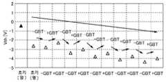
도 65는 임계 전압의 변동 및 시프트값의 차이를 나타낸다.
도 66은 임계 전압의 변동 및 3개 신호의 스핀 밀도의 합 및 산화질화 실리콘막으로부터 방출된 질화 산화물과 산소의 양에 따르는 시프트값의 상관관계를 나타낸다.
도 67은 SIMS의 측정결과를 나타낸다.
도 68은 SIMS의 측정결과를 나타낸다.
도 69(A) 및 69(B)는 단면 STEM상이다.
도 70(A) 및 70(B)은 각각 비교예의 전기 특성을 나타낸다.
도 71(A)~71(C)은 각각 실시예 시료의 전기 특성을 나타낸다.
도 72(A) 및 72(B)는 각각 실시예 시료의 전기 특성을 나타낸다.
도 73(A) 및 73(B)은 각각 실시예 시료의 전기 특성을 나타낸다.1 (A) to 1 (C) are a top view and a cross-sectional view showing a transistor.
2 (A) to 2 (C) show a method for forming a transistor.
3 (A) to 3 (C) show a method for forming a transistor.
4 (A) to 4 (D) show a method for forming a transistor.
5 (A) to 5 (C) are a top view and a cross-sectional view showing a transistor.
6 (A) to 6 (C) are cross-sectional views each showing a transistor.
7 (A) to 7 (C) are a top view and a cross-sectional view showing a transistor.
8 (A) to 8 (D) each show the band structure of the transistor.
9 (A) and 9 (B) are cross-sectional views showing transistors.
10 (A) to 10 (C) are cross-sectional views each showing a transistor.
11 (A) to 11 (C) are cross-sectional views each showing a transistor.
12 (A) to 12 (C) are cross-sectional views each showing a transistor.
13 (A) to 13 (C) are a top view and a cross-sectional view showing the transistor.
14 (A) to 14 (C) show a method for forming a transistor.
15 (A) to 15 (C) show a method for forming a transistor.
16 (A) to 16 (C) are cross-sectional views each showing a transistor.
17 (A) to 17 (C) are a top view and a cross-sectional view showing the transistor.
18 (A) to 18 (C) are cross-sectional views each showing a transistor.
19 (A) to 19 (C) are cross-sectional views each showing a transistor.
20 (A) to 20 (C) are cross-sectional views each showing a transistor.
Figures 21 (A) and 21 (B) show the relationship between the formation energy and the transition level and the electronic arrangement of defects.
Fig. 22 shows the change in the Fermi level and the change in the charge state of the defect.
23 shows a crystalline model of c-SiO2 .
24 is a c-SiO2 And a model in which NO2 is introduced into a clearance of the model.
25 is a c-SiO2 This shows a model in which N2 O is introduced into the gap of the model.
26 is a c-SiO2 This shows a model in which NO is introduced into a clearance of the model.
FIG. 27 is a cross-sectional view of c-SiO2 It represents a model in which N atoms are introduced into the gap of the model.
28 is a band diagram.
29 (A) and 29 (B) show models of the cluster structure, respectively.
Figure 30 shows the mechanism of the phenomenon of shifting the threshold voltage of the transistor in the positive direction.
31 (A) to 31 (D) show a bulk model.
32 shows the structure of the model.
33 (A) and 33 (B) show the relationship between the formation energy of VO H and the transition level and the thermodynamic transition level of VO H.
34 shows the relationship between the carrier density and the defect density of VO H.
FIG. 35 shows the band structure of the DOS in the oxide semiconductor film and in the vicinity of the oxide semiconductor film interface.
36 is a graph showing deterioration of a transistor including an oxide semiconductor film in a dark state.
37 shows deterioration of a transistor including an oxide semiconductor film in a dark state.
38 is a graph showing deterioration of a transistor including an oxide semiconductor film under light irradiation.
FIG. 39 shows deterioration of a transistor including an oxide semiconductor film under light irradiation.
40 shows deterioration of a transistor including an oxide semiconductor film under light irradiation.
41 (A) to 41 (F) show a model in which the oxide semiconductor film is highly purified so as to become intact.
42 (A) to 42 (D) are cross-sectional schematic views of a Cs-corrected high-resolution TEM image and a CAAC-OS film of a cross-section of a CAAC-OS film.
43 (A) to 43 (D) are Cs-corrected high resolution TEM images of the CAAC-OS film plane.
44 (A) to 44 (C) show structural analysis of a CAAC-OS film and a single crystal oxide semiconductor film by XRD.
45 (A) and 45 (B) show electron diffraction patterns of a CAAC-OS film.
46 shows a change in crystal part of the In-Ga-Zn oxide induced by electron irradiation.
47 (A) and 47 (B) are schematic views showing a deposition model of a CAAC-OS film and an nc-OS film.
Figure 48 (A) ~ 48 (C ) shows the InGaZnO4 crystals and pellets.
49 (A) to 49 (D) are schematic views showing a deposition model of a CAAC-OS film.
50 (A) to 50 (D) are a cross-sectional view and a circuit diagram showing a semiconductor device, respectively.
51 (A) to 51 (C) are a circuit diagram and a sectional view showing a memory device, respectively.
Fig. 52 shows a configuration example of an RF tag.
53 shows a configuration example of a CPU.
54 is a circuit diagram of a memory device.
FIG. 55A shows a configuration example of the display device, and FIGS. 55B and 55C are circuit diagrams of pixels.
56 shows a display module.
57 (A) to 57 (F) show electronic devices, respectively.
58 (A) to 58 (F) show application examples of RF devices, respectively.
59 (A) to 59 (C) show ESR measurement results.
60 shows the ESR measurement result.
Figure 61 shows the measurement results of the TDS analysis.
Figure 62 shows the measurement results of the TDS analysis.
Figure 63 shows the measurement results of the TDS analysis.
Figure 64 shows the relationship between the partial pressure of oxygen and the amount of gas released according to each molecular weight.
65 shows the variation of the threshold voltage and the difference of the shift value.
66 shows a correlation between the variation of the threshold voltage and the sum of the spin densities of the three signals and the shift value according to the amount of oxygen oxide and oxygen emitted from the silicon oxynitride film.
67 shows the results of SIMS measurement.
68 shows the measurement result of SIMS.
69 (A) and 69 (B) are sectional STEM images.
70 (A) and 70 (B) show electrical characteristics of the comparative example, respectively.
Figs. 71 (A) to 71 (C) show electrical characteristics of the sample of the embodiment.
72 (A) and 72 (B) show electrical characteristics of the sample of the example, respectively.
73 (A) and 73 (B) show the electrical characteristics of the sample of the example, respectively.
본 발명의 실시형태는 도면을 참조하여 상세하게 후술된다. 또한, 본 발명은 하기 설명에 제한되는 것은 아니고, 본 발명의 취지 및 범위에서 벗어나는 것 없이 그 형태 및 세부사항을 다양하게 변화시킬 수 있다는 것이 당업자에게 용이하게 이해된다. 따라서, 본 발명은 하기 실시형태 및 실시예의 설명에 제한되어 해석되는 것은 아니다. 또한, 하기 실시형태 및 실시예에서, 동일한 부분 또는 유사한 기능을 갖는 부분은 상이한 도면에서 동일한 참조 번호 또는 동일한 해칭 패턴에 의해 나타나고, 그 설명은 반복되지 않는다.Embodiments of the present invention will be described in detail below with reference to the drawings. It is also to be understood by those skilled in the art that the present invention is not limited to the following description, and that various changes in form and detail can be made without departing from the spirit and scope of the present invention. Therefore, the present invention is not construed as being limited to the description of the embodiments and examples described below. Furthermore, in the following embodiments and examples, portions having the same or similar functions are represented by the same reference numerals or the same hatching pattern in different drawings, and description thereof is not repeated.
또한, 본 명세서에 기재된 각각의 도면에서, 각 구성 요소의 크기, 막 두께, 또는 영역은 명료화를 위해 과장되는 경우가 있다. 따라서, 본 발명의 실시형태는 이러한 규모에 제한되는 것은 아니다.Further, in each of the drawings described in this specification, the size, the film thickness, or the area of each component may be exaggerated for clarity. Therefore, the embodiment of the present invention is not limited to this scale.
또한, 본 명세서에서 "제 1", "제 2", 및 "제 3"과 같은 용어는 구성 요소 중에서 혼동을 피하기 위해서 사용되고, 용어는 수적으로 구성 요소를 제한하지 않는다. 따라서, 예를 들면 용어 "제 1"은 용어 "제 2", "제 3" 등으로 적절하게 대체될 수 있다.In addition, terms such as " first, "" second, "and " third" are used herein to avoid confusion among components, and the term does not limit components numerically. Thus, for example, the term " first "may be appropriately substituted with the terms" second ", "third"
"소스" 및 "드레인"의 기능은, 예를 들면 회로 동작에서 전류 흐름의 방향이 변화되는 경우 가끔 서로 대체된다. 따라서, 용어 "소스" 및 "드레인"은 본 명세서에서 각각 드레인 및 소스를 나타내는데 사용된다.The functions of "source" and "drain" are sometimes interchanged, for example, when the direction of current flow in a circuit operation is changed. Thus, the terms "source" and "drain" are used herein to denote a drain and a source, respectively.
또한, 전압이란 2점 전위 간의 차이를 말하고, 전위란 정전기장의 주어진 일점에서 단위 전하의 정전기 에너지(전기력에 의한 위치에너지)를 말한다. 또한, 일반적으로 일점의 전위와 기준 전위(예를 들면, 접지 전위) 간의 차이는 단순하게 전위 또는 전압이라 불리고, 전위 및 전압은 동의어로서 사용되는 경우가 많다. 따라서, 본 명세서에서, 전위는 전압이라 바꾸어 말할 수 있고 전압은 달리 특정하지 않는 한 전위라 바꾸어 말할 수 있다.The term " voltage " refers to a difference between two-point potentials, and the term " potential " refers to the electrostatic energy (potential energy by electric force) of a unit electric charge at a given point in the static electric field. Further, in general, a difference between a potential at one point and a reference potential (for example, a ground potential) is simply referred to as a potential or voltage, and a potential and a voltage are often used as synonyms. Thus, in this specification, the potential can be said to be a voltage, and the voltage can be said to be a potential unless otherwise specified.
또한, 산화물 반도체막을 포함하는 트랜지스터는 n-채널 트랜지스터이므로; 본 명세서에서 게이트 전압이 0V인 경우 드레인 전류가 그 안에서 흐르지 않는 것으로 간주될 수 있는 트랜지스터는 노멀리-오프 특성을 갖는 트랜지스터라 정의된다. 반대로, 게이트 전압이 0V인 경우 드레인 전류가 그 안에서 흐르는 것으로 간주될 수 있는 트랜지스터는 노멀리-온 특성을 갖는 트랜지스터라 정의된다.Further, since the transistor including the oxide semiconductor film is an n-channel transistor; In this specification, a transistor in which a drain current can be regarded as not flowing in the case where the gate voltage is 0V is defined as a transistor having a normally-off characteristic. Conversely, when the gate voltage is 0V, a transistor whose drain current can be regarded as flowing in it is defined as a transistor having a normally-on characteristic.
또한, 채널 길이란, 예를 들면 트랜지스터의 상면도에 있어서 산화물 반도체막(또는 트랜지스터가 온인 경우 산화물 반도체막에 전류가 흐르는 부분)과 게이트 전극이 서로 중첩하는 영역 또는 채널이 형성되는 영역에서의 소스(소스 영역 또는 소스 전극)와 드레인(드레인 영역 또는 드레인 전극) 사이의 거리를 말한다. 하나의 트랜지스터에 있어서, 모든 영역에서의 채널 길이가 반드시 동일할 필요는 없다. 즉, 하나의 트랜지스터의 채널 길이는 하나의 값에 제한되지 않는 경우가 있다. 따라서, 본 명세서에서 채널 길이는 채널이 형성되는 영역에서의 값, 최대값, 최소값, 또는 평균값 중의 어느 하나이다.The channel length is, for example, a region in which an oxide semiconductor film (or a portion where a current flows in the oxide semiconductor film when the transistor is on) and a gate electrode overlap each other in a top view of a transistor or a source (Source region or source electrode) and drain (drain region or drain electrode). In one transistor, the channel lengths in all regions do not necessarily have to be the same. That is, the channel length of one transistor may not be limited to one value. Thus, in this specification, the channel length is either a value, a maximum value, a minimum value, or an average value in a region where a channel is formed.
채널 폭이란, 예를 들면 산화물 반도체막(또는 트랜지스터가 온인 경우 산화물 반도체막에 전류가 흐르는 부분)과 게이트 전극이 서로 중첩하는 영역 또는 채널이 형성되는 영역에서의 소스 또는 드레인의 폭을 말한다. 하나의 트랜지스터에 있어서, 모든 영역에서의 채널 폭이 반드시 동일할 필요는 없다. 즉, 하나의 트랜지스터의 채널 폭은 하나의 값으로 제한되지 않는 경우가 있다. 따라서, 본 명세서에서 채널 폭은 채널이 형성되는 영역에서의 값, 최대값, 최소값, 또는 평균값 중의 어느 하나이다.The channel width refers to a width of a source or a drain in a region where an oxide semiconductor film (or a portion where a current flows in the oxide semiconductor film when the transistor is on) and a gate electrode overlap each other or a region where a channel is formed. In one transistor, the channel widths in all regions do not necessarily have to be the same. That is, the channel width of one transistor may not be limited to one value. Thus, in this specification, the channel width is either a value, a maximum value, a minimum value, or an average value in a region where a channel is formed.
또한, 트랜지스터 구조에 따라 채널이 실제로 형성되는 영역에서의 채널 폭(이하, 유효 채널 폭이라 불림)은 트랜지스터의 상면도에 나타낸 채널 폭(이하, 겉보기 채널 폭이라 불림)과 다른 경우가 있다. 예를 들면, 3차원 구조를 갖는 트랜지스터에서 유효 채널 폭은 트랜지스터의 상면도에 나타낸 겉보기 채널 폭보다 크고, 그것의 영향은 무시할 수 없는 경우가 있다. 예를 들면, 3차원 구조를 갖는 소형화된 트랜지스터에서 산화물 반도체막의 측면에 형성된 채널 영역의 비율은 산화물 반도체막의 상면에 형성된 채널 영역의 비율보다 높은 경우가 있다. 그 경우에 있어서, 채널이 실제로 형성되는 경우 얻어지는 유효 채널 폭은 상면도에 나타낸 겉보기 채널 폭보다 크다.In addition, the channel width (hereinafter referred to as an effective channel width) in a region where a channel is actually formed according to a transistor structure may be different from a channel width (hereinafter referred to as an apparent channel width) shown in a top view of the transistor. For example, in a transistor having a three-dimensional structure, the effective channel width is larger than the apparent channel width shown in the top view of the transistor, and the influence thereof may not be negligible. For example, in a miniaturized transistor having a three-dimensional structure, the ratio of the channel region formed on the side surface of the oxide semiconductor film may be higher than the ratio of the channel region formed on the top surface of the oxide semiconductor film. In that case, the effective channel width obtained when the channel is actually formed is larger than the apparent channel width shown in the top view.
3차원 구조를 갖는 트랜지스터에서 유효 채널 폭을 측정하기 어려운 경우가 있다. 예를 들면, 설계값으로부터 유효 채널 폭의 추정은 산화물 반도체막의 형상이 알려져 있는 가정을 필요로 한다. 따라서, 산화물 반도체막의 형상이 정확하게 알려져 있지 않은 경우에 유효 채널 폭을 정확하게 측정하기가 어렵다.It may be difficult to measure the effective channel width in a transistor having a three-dimensional structure. For example, the estimation of the effective channel width from the design value requires the assumption that the shape of the oxide semiconductor film is known. Therefore, it is difficult to accurately measure the effective channel width when the shape of the oxide semiconductor film is not accurately known.
따라서, 본 명세서에서 트랜지스터의 상면도에 있어서, 겉보기 채널 폭, 즉 산화물 반도체막과 게이트 전극이 서로 중첩하는 영역에서의 소스 또는 드레인의 폭은 둘러싸인 채널 폭(SCW)이라 불리는 경우가 있다. 또한, 본 명세서에서 용어 "채널 폭"이 단순하게 사용되는 경우에 그것은 둘러싸인 채널 폭 또는 겉보기 채널 폭을 나타낼 수 있다. 또한, 본 명세서에서 용어 "채널 폭"이 단순하게 사용되는 경우에 그것은 유효 채널 폭을 나타내는 경우가 있다. 또한, 채널 길이, 채널 폭, 유효 채널 폭, 겉보기 채널 폭, 둘러싸인 채널 폭 등의 값은 단면 TEM상 등을 얻어 해석함으로써 결정될 수 있다.Therefore, in the top view of the transistor in this specification, the width of the source or drain in the region where the apparent channel width, that is, the region where the oxide semiconductor film and the gate electrode overlap with each other, is sometimes called the enclosed channel width (SCW). In addition, where the term "channel width" is simply used herein, it may indicate the enclosed channel width or the apparent channel width. Also, in this specification, when the term "channel width" is simply used, it may indicate the effective channel width. In addition, values such as channel length, channel width, effective channel width, apparent channel width, enclosed channel width, and the like can be determined by obtaining and analyzing cross-sectional TEM images or the like.
또한, 트랜지스터의 전계-효과 이동도, 채널 폭 당 전류값 등이 산출에 의해 얻어지는 경우 둘러싸인 채널 폭은 산출용으로 사용될 수 있다. 그 경우에 있어서, 값은 유효 채널 폭을 사용하여 산출되는 것과 다를 수 있는 경우가 있다.In addition, when the electric field-effect mobility of the transistor, the current value per channel width, or the like is obtained by calculation, the enclosed channel width can be used for calculation. In that case, the value may be different from that calculated using the effective channel width.
본 명세서에 있어서, 용어 "평행"이란 2개의 직선 사이에 형성된 각이 -10°이상 및 10°이하이므로, 각이 -5°이상 및 5°이하인 경우도 포함한다는 것을 나타낸다. 용어 "실질적으로 평행"이란 2개의 직선 사이에 형성된 각이 -30°이상 및 30°이하인 것을 나타낸다. 용어 "수직"이란 2개의 직선 사이에 형성된 각이 80°이상 및 100°이하이므로, 각이 85°이상 및 95°이하인 경우를 포함한다는 것을 나타낸다. 용어 "실질적으로 수직"이란 2개의 직선 사이에 형성된 각이 60°이상 및 120°이하인 것을 나타낸다.In the present specification, the term "parallel" means that an angle formed between two straight lines is not less than -10 degrees and not more than 10 degrees, and thus includes angles of not less than -5 degrees and not more than 5 degrees. The term "substantially parallel" means that an angle formed between two straight lines is not less than -30 degrees and not more than 30 degrees. The term "vertical" indicates that an angle formed between two straight lines is not less than 80 ° and not more than 100 °, and thus includes an angle of not less than 85 ° and not more than 95 °. The term "substantially vertical" indicates that an angle formed between two straight lines is 60 degrees or more and 120 degrees or less.
본 명세서에 있어서, 삼방정계 및 능면정계는 육방정계에 포함된다.In the present specification, the triangular system and the surface-facing system are included in the hexagonal system.
(실시형태 1)(Embodiment 1)
본 실시형태에 있어서, 본 발명의 일 실시형태의 반도체 장치 및 반도체 장치를 제조하기 위한 방법에 대해서 도면을 참조하여 설명한다. 본 실시형태에 기재된 트랜지스터(10)는 이중 게이트 구조를 갖는다.In the present embodiment, a method for manufacturing a semiconductor device and a semiconductor device according to an embodiment of the present invention will be described with reference to the drawings. The
<1. 트랜지스터의 구조><1. Transistor Structure>
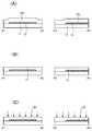
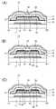
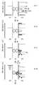
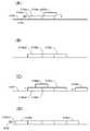
도 1(A)~1(C)은 반도체 장치에 포함되는 트랜지스터(10)의 상면도 및 단면도이다. 도 1(A)은 트랜지스터(10)의 상면도이고, 도 1(B)은 도 1(A)의 일점쇄선 A1-A2를 따라 취해진 단면도이며, 도 1(C)은 도 1(A)의 일점쇄선 A3-A4를 따라 취해진 단면도이다. 도 1(A)~1(C)에 있어서, 이해를 용이하게 하기 위해서 몇몇 구성 요소를 확대, 크기 감소, 또는 생략한다. 몇몇 경우에 있어서, 일점쇄선 A1-A2의 방향을 채널 길이 방향이라 불리고, 일점쇄선 A3-A4의 방향을 채널 폭 방향이라 부른다.1 (A) to 1 (C) are a top view and a cross-sectional view of a
도 1(A)~1(C)에 도시된 트랜지스터(10)는 기판(11) 상에 도전막(12), 기판(11)과 도전막(12) 상에 베이스 절연막(13), 베이스 절연막(13) 상에 산화물 반도체막(14), 베이스 절연막(13) 및 산화물 반도체막(14)과 접하는 산화 방지막(20), 산화 방지막(20) 상에 한 쌍의 전극(15, 16), 한 쌍의 전극(15, 16) 상에 게이트 절연막(17), 및 게이트 절연막(17)을 통해서 산화물 반도체막(14)과 중첩하는 게이트 전극(18)을 포함한다. 절연막(19)은 게이트 절연막(17) 및 게이트 전극(18) 상에 형성될 수 있다.The
절연막(19)은 산소, 수소, 물 등을 차단하는 배리어막으로서 기능한다. 이것은 절연막(19)이 수소 및 물을 외부로부터 산화물 반도체막(14)을 침입하는 것을 방지할 수 있고 산화물 반도체막의 산소가 외부에 방출되는 것을 방지할 수 있다는 것을 의미한다.The insulating
산화 방지막(20)은 한 쌍의 전극(15, 16) 하에 직접적으로 제공된다. 산화 방지막(20)은 베이스 절연막(13)으로부터 방출되는 산소에 의해 유도된 한 쌍의 전극의 산화를 억제한다. 이런 이유로 인해, 산화로 인한 한 쌍의 전극(15, 16)의 부피 팽창을 억제할 수 있고 게이트 절연막(17)과 한 쌍의 전극(15, 16)의 피복성을 개선시킬 수 있다.The
산화 방지막(20)에 있어서, 한 쌍의 전극(15, 16)과 중첩하는 영역의 폭은 한 쌍의 전극(15, 16)과 중첩하지 않는 영역의 폭보다 길다. 따라서, 트랜지스터의 소형화로 이어지는 한 쌍의 전극(15, 16)과 중첩하지 않는 영역의 폭은 짧을 수 있고, 접촉 내성의 감소로 이어지는 산화 방지막(20)이 한 쌍의 전극(15, 16)과 접하는 영역의 부분이 증가될 수 있다.In the
산화 방지막(20)으로서, 베이스 절연막(13)에서의 산소가 한 쌍의 전극(15, 16)에 도달하는 것을 방지하는 어느 하나의 막이 사용될 수 있다. 예를 들면, 1:1:1, 1:3:4, 1:3:6, 1:3:8, 또는 1:4:5의 원자비에서 In, Ga, 및 Zn을 함유하는 타겟을 사용하여 스퍼터링법에 의해 형성되는 In-Ga-Zn 산화물 반도체막이 사용될 수 있다.As the
본 실시형태에 있어서, 산화물 반도체막(14)과 가깝게 위치되는 막, 대표예로서 베이스 절연막(13)과 게이트 절연막(17) 중 적어도 하나는 질소를 함유하고 작은 결함수를 갖는 산화물 절연막이 바람직하다.In the present embodiment, at least one of the films positioned close to the oxide semiconductor film 14 (typically, the
질소를 함유하고 작은 결함수를 갖는 산화물 절연막의 대표예로는 산화질화 실리콘막 및 산화질화 알루미늄막을 포함한다. 또한, 산화질화 실리콘막 또는 산화질화 알루미늄막과 같은 "산화질화막"은 질소보다 산소를 더 많이 함유하는 막을 말하고, 질화산화 실리콘막 또는 질화산화 알루미늄막과 같은 "질화산화막"은 산소보다 질소를 더 많이 함유하는 막을 말한다.Typical examples of the oxide insulating film containing nitrogen and having a small number of defects include a silicon oxynitride film and an aluminum oxynitride film. Further, a "nitrided oxide film" such as a silicon oxynitride film or an aluminum oxynitride film is a film containing more oxygen than nitrogen, and a "nitrided oxide film" such as a silicon nitride oxide film or an aluminum nitride oxide film, It refers to a membrane containing a lot.
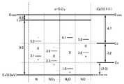
작은 결함수를 갖는 산화물 절연막의 100 K 이하에서의 ESR 스펙트럼에 있어서, 2.037 이상 및 2.039 이하의 g 인자에서 나타나는 제 1 신호, 2.001 이상 및 2.003 이하의 g 인자에서 나타나는 제 2 신호, 및 1.964 이상 및 1.966 이하의 g 인자에서 나타나는 제 3 신호가 관찰된다. 본 실시형태에 있어서, "신호가 관찰된다"란 4.7×10¹⁵ 스핀/㎤ 이상의 스핀 밀도가 g 인자에서 관찰되는 것을 의미한다. X 밴드를 사용한 ESR 측정에 의해 얻어지는 제 1과 제 2 신호의 스플릿 폭 및 제 2와 제 3 신호의 스플릿 폭은 각각 약 5 mT이다. 제 1~제 3 신호의 스핀 밀도의 합은 4×10¹⁸ 스핀/㎤ 미만, 대표적으로 2.4×10¹⁸ 스핀/㎤ 이상 및 4×10¹⁸ 스핀/㎤ 미만이다.A first signal appearing at a g factor of 2.037 or more and 2.039 or less, a second signal appearing at a g factor of 2.001 or more and 2.003 or less, and a second signal appearing at an impurity concentration of 1.964 or more in an ESR spectrum of an oxide insulating film having a small number of defects, A third signal appears at a g factor of 1.966 or less. In the present embodiment, "a signal is observed" means that a spin density of 4.7 × 10¹⁵ spins /
100 K 이하에서의 ESR 스펙트럼에 있어서, 2.037 이상 및 2.039 이하의 g 인자에서 나타나는 제 1 신호, 2.001 이상 및 2.003 이하의 g 인자에서 나타나는 제 2 신호, 및 1.964 이상 및 1.966 이하의 g 인자에서 나타나는 제 3 신호는 질소 산화물(NOx; x는 0 초과 및 2 이하, 바람직하게 1 이상 및 2 이하)에 기인되는 신호와 대응된다. 질소 산화물의 대표예는 일산화질소 및 이산화질소를 포함한다. 즉, 2.037 이상 및 2.039 이하의 g 인자에서 나타나는 제 1 신호, 2.001 이상 및 2.003 이하의 g 인자에서 나타나는 제 2 신호, 및 1.964 이상 및 1.966 이하의 g 인자에서 나타나는 제 3 신호의 총 스핀 밀도가 적을수록 산화물 절연막의 질소 산화물의 함량이 작다.A first signal appearing at a g-factor of not less than 2.037 and not more than 2.039, a second signal appearing at a g-factor of not less than 2.001 and not more than 2.003 in an ESR spectrum at not more than 100 K, and a second signal appearing at a g- 3 signal corresponds to a signal attributable to nitrogen oxides (NOx, where x is more than 0 and not more than 2, preferably not less than 1 and not more than 2). Representative examples of nitrogen oxides include nitrogen monoxide and nitrogen dioxide. That is, the first signal appearing at a g factor of 2.037 or more and 2.039 or less, the second signal appearing at a g factor of 2.001 or more and 2.003 or less, and the third signal appearing at a g factor of 1.964 or more and 1.966 or less, The content of nitrogen oxides in the oxide insulating film is small.
질소를 함유하고 작은 결함수를 갖는 산화물 절연막에 있어서, 증착 온도가 증가할수록 질소 농도 및 수소 농도는 낮아지게 된다. 산화물 절연막의 대표적인 증착 온도는 500℃ 이상, 바람직하게 500℃ 이상 및 550℃ 이하이다. 질소 농도가 감소된 후에 산소가 첨가되는 경우, 질소 산화물의 발생이 억제될 수 있으므로, 산화물 절연막에 산소가 첨가될 수 있고 산화물 반도체막(14)에 공급될 수 있다.In an oxide insulating film containing nitrogen and having a small number of defects, the nitrogen concentration and the hydrogen concentration become lower as the deposition temperature increases. The typical deposition temperature of the oxide insulating film is 500 占 폚 or higher, preferably 500 占 폚 or higher and 550 占 폚 or lower. When oxygen is added after the nitrogen concentration is reduced, the generation of nitrogen oxides can be suppressed, so that oxygen can be added to the oxide insulating film and supplied to the
산화물 반도체막(14) 가까이에 위치된 베이스 절연막(13) 및 게이트 절연막(17) 중 적어도 하나가 상술한 바와 같이 소량의 질소 산화물을 함유하는 경우, 베이스 절연막(13)과 산화물 반도체막(14) 사이의 계면에서 캐리어 트랩이 억제될 수 있다. 따라서, 반도체 장치에 포함되는 트랜지스터의 임계 전압의 시프트가 억제될 수 있고, 이것은 트랜지스터 전기 특성의 감소된 변화로 이어진다.When the
베이스 절연막(13) 및 게이트 절연막(17) 중 적어도 하나는 이차 이온 질량분석(SIMS)에 의해 측정된 질소 농도가 1×10²⁰ 원자/㎤ 미만인 부분을 갖는 것이 바람직하다. 그 경우에 있어서, 질소 산화물은 베이스 절연막(13) 및 게이트 절연막(17) 중 적어도 하나에서 발생될 가능성이 낮아 베이스 절연막(13)과 산화물 반도체막(14) 사이의 계면에 캐리어 트랩이 억제될 수 있다. 또한, 반도체 장치에 포함되는 트랜지스터의 임계 전압의 시프트가 억제될 수 있고, 이것은 트랜지스터의 전기 특성의 감소된 변화로 이어진다.It is preferable that at least one of the
베이스 절연막(13) 및 게이트 절연막(17) 중 적어도 하나는 SIMS에 의해 측정된 수소 농도가 5×10²⁰ 원자/㎤ 미만인 부분을 포함하는 것이 바람직하다. 산화물 반도체막(14) 가까이에 위치된 베이스 절연막(13) 및 게이트 절연막(17)의 낮은 수소 농도는 수소가 산화물 반도체막(14)을 침입하는 것을 방지할 수 있다.It is preferable that at least one of the
트랜지스터(10)의 다른 구성 요소의 세부사항에 대해서 후술한다.Details of other components of the
재료가 적어도 후 열처리에 견디기 충분한 내열성을 가지기만 하면 기판(11)의 재료 등의 특성에 특별히 제한되지 않는다. 예를 들면, 유리 기판, 세라믹 기판, 석영 기판, 또는 사파이어 기판은 기판(11)으로서 사용될 수 있다. 또한, 실리콘, 탄화 실리콘 등으로 이루어진 단결정 반도체 기판 또는 다결정 반도체 기판, 실리콘 게르마늄 등으로 이루어진 화합물 반도체 기판, 실리콘 온 인슐레이터(SOI) 기판 등은 기판(11)으로서 사용될 수 있다. 또한, 반도체 소자가 더 제공된 이들 기판 중 어느 하나가 기판(11)으로서 사용될 수 있다.The material is not particularly limited to the characteristics of the material of the
또한, 가요성 기판은 기판(11)으로서 사용될 수 있고, 트랜지스터(10)는 가요성 기판에 직접적으로 제공될 수 있다. 또한, 박리층은 기판(11)과 트랜지스터(10) 사이에 제공될 수 있다. 박리층 상에 형성된 반도체 장치의 일부 또는 전체가 기판으로부터 박리되어 또 다른 기판 상에 이송되는 경우 박리층이 사용될 수 있다. 이러한 경우에 있어서, 낮은 내열성을 갖는 기판 또는 가요성 기판도 트랜지스터(10)에 이송될 수 있다.Further, the flexible substrate can be used as the
도전막(12)은 알루미늄, 크롬, 구리, 탄탈, 티타늄, 몰리브덴, 및 텅스텐으로부터 선택되는 금속 원소; 이들 금속 원소 중 어느 하나를 구성 요소로서 함유하는 합금; 이들 금속 원소를 조합해서 함유하는 합금 등을 사용하여 형성할 수 있다. 망간 및 지르코늄으로부터 선택되는 하나 이상의 금속 원소를 사용할 수 있다. 도전막(12)은 단층 구조 또는 2층 이상의 적층 구조를 가질 수 있다. 예를 들면, 하기: 실리콘을 함유하는 알루미늄막의 단층 구조; 티타늄막이 알루미늄막 상에 적층된 2층 구조; 티타늄막이 질화 티타늄막 상에 적층된 2층 구조; 텅스텐막이 질화 티타늄막 상에 적층된 2층 구조; 텅스텐막이 질화 탄탈막 또는 질화 텅스텐막 상에 적층된 2층 구조; 티타늄막, 알루미늄막, 및 티타늄막이 순서대로 적층된 3층 구조 등 중 어느 하나를 사용할 수 있다. 또한, 알루미늄 및 티타늄, 탄탈, 텅스텐, 몰리브덴, 크롬, 네오디뮴, 및 스칸듐으로부터 선택된 하나 이상의 원소를 함유하는 합금막 또는 질화막을 사용할 수 있다.The
도전막(12)은 인듐 주석 산화물, 산화 텅스텐을 함유하는 인듐 산화물, 산화 텅스텐을 함유하는 인듐 아연 산화물, 산화 티타늄을 함유하는 인듐 산화물, 산화 티타늄을 함유하는 인듐 주석 산화물, 인듐 아연 산화물, 산화 실리콘을 함유하는 인듐 주석 산화물, 산화 마그네슘을 함유하는 인듐 산화물 화합물, 산화 갈륨을 함유하는 아연 산화물, 산화 알루미늄을 함유하는 아연 산화물, 산화 마그네슘을 함유하는 아연 산화물, 또는 플루오르를 함유하는 주석 산화물과 같은 투광성 도전 재료를 사용하여 형성될 수도 있다. 상기 투광성 도전 재료 중 어느 하나 및 상기 금속 원소 중 어느 하나를 사용하여 형성된 적층 구조를 채용하는 것도 가능해진다. The
도전막(12)은 게이트 전극으로서 기능하고 백 게이트로서 사용될 수 있으므로 온-상태의 전류를 더 증가시키고 임계 전압을 제어하는데 사용될 수 있다. 온-상태의 전류를 증가시키기 위해서, 예를 들면 게이트 전극(18) 및 도전막(12)은 동일한 전위를 갖기 위해 서로 전기적으로 접속되고, 트랜지스터는 이중 게이트 트랜지스터로서 구동된다. 임계 전압을 제어하기 위해서, 게이트 전극(18)의 전위와 다른 고정된 전위가 도전막(12)에 공급되도록 게이트 전극(18) 및 도전막(12)은 서로 전기적으로 접속되지 않는다. 또한, 게이트 전극(18)은 도전막(12)용 재료 중 어느 하나를 사용하여 형성될 수 있다.The
베이스 절연막(13)은, 예를 들면 산화 실리콘, 산화질화 실리콘, 질화 실리콘, 질화산화 실리콘, 산화 갈륨, 산화 하프늄, 산화 이트륨, 산화 알루미늄, 또는 산화질화 알루미늄을 사용하여 형성될 수 있다. 또한, 질화 실리콘, 산화 갈륨, 산화 하프늄, 산화 이트륨, 산화 알루미늄 등이 베이스 절연막(13)에 사용되는 경우, 기판(11) 측으로부터 알칼리 금속, 물, 및 수소와 같은 불순물을 산화물 반도체막(14)으로 확산시키는 것을 억제하는 것이 가능해진다.The
베이스 절연막(13)이 질소를 함유하고 작은 결함수를 갖는 산화물 절연막을 사용하여 형성되는 경우에 있어서, 게이트 절연막(17)은, 예를 들면 산화 실리콘, 산화질화 실리콘, 질화산화 실리콘, 질화 실리콘, 산화 알루미늄, 산화 하프늄, 산화 갈륨, Ga-Zn계 금속 산화물 등 중 어느 하나를 사용한 단층 구조 또는 적층 구조를 갖도록 형성될 수 있다. 또한, 산화물 반도체막(14)과의 계면 특성을 개선시키기 위해서 적어도 게이트 절연막(17)의 영역에 산화물 절연막이 사용되는 것이 바람직하고, 이것은 산화물 반도체막(14) 가까이에 위치된다.In the case where the
또한, 게이트 절연막(17)으로서 산소, 수소, 물 등에 대하여 차단 효과를 갖는 절연막을 제공함으로써 산화물 반도체막(14)으로 산소의 외부 확산 및 외부로부터 산화물 반도체막(14)으로 수소, 물 등의 침입을 방지하는 것이 가능해진다. 산소, 수소, 물 등에 대하여 차단 효과를 갖는 절연막으로서, 산화 알루미늄막, 산화질화 알루미늄막, 산화 갈륨막, 산화질화 갈륨막, 산화 이트륨막, 산화질화 이트륨막, 산화 하프늄막, 및 산화질화 하프늄막이 실시예로서 주어질 수 있다.In addition, by providing an insulating film having a blocking effect against oxygen, hydrogen, water, etc. as the
게이트 절연막(17)은 하프늄 실리케이트(HfSiOx), 질소가 첨가된 하프늄 실리케이트(HfSixOy), 질소가 첨가된 하프늄 알루미네이트(HfAlxOy), 산화 하프늄, 또는 산화 이트륨과 같은 하이-k 재료를 사용하여 형성될 수 있어서 트랜지스터의 게이트 누전을 감소시킬 수 있다.The
산화물 반도체막(14)은 적어도 In 또는 Zn을 함유하는 금속 산화물을 사용하여 형성되고; 대표예로서 In-Ga 산화물, In-Zn 산화물, In-Mg 산화물, Zn-Mg 산화물, 또는 In-M-Zn 산화물(M은 Al, Ga, Sn, Y, Zr, La, Ce, Mg, 또는 Nd임)을 들 수 있다.The
또한, 산화물 반도체막(14)이 In-M-Zn 산화물을 함유하는 경우, Zn 및 O를 고려하지 않은 In 및 M의 비율은 하기: In의 비율은 25 원자% 이상이고 M의 비율은 75 원자% 미만이 바람직하거나, In의 비율은 34 원자% 이상이고 M의 비율은 66 원자% 미만이 더욱 바람직하다.In the case where the
산화물 반도체막(14)의 에너지 갭은 2 eV 이상, 바람직하게 2.5 eV 이상, 더욱 바람직하게 3 eV 이상이다. 이러한 넓은 에너지 갭을 갖는 산화물 반도체의 사용으로 트랜지스터(10)의 오프-상태 전류는 감소될 수 있다.The energy gap of the
산화물 반도체막(14)의 두께는 3 ㎚ 이상 및 200 ㎚ 이하, 바람직하게 3 ㎚ 이상 및 100 ㎚ 이하, 더욱 바람직하게 3 ㎚ 이상 및 50 ㎚ 이하이다.The thickness of the
산화물 반도체막(14)이 In-M-Zn 산화물(M은 Al, Ga, Y, Zr, La, Ce, Mg, 또는 Nd를 나타냄)을 함유하는 경우, In-M-Zn 산화물의 막을 형성하기 위해 사용되는 스퍼터링 타겟의 금속 원소의 원자비는 In≥≥M 및 Zn≥M을 만족하는 것이 바람직하다. 이러한 스퍼터링 타겟의 금속 원소의 원자비로서, In:M:Zn=1:1:1, In:M:Zn=1:1:1.2, 및 In:M:Zn=3:1:2가 바람직하다. 또한, 형성된 산화물 반도체막(14)의 금속 원소의 원자비는 오차로서 ±40% 범위 내의 스퍼터링 타겟의 금속 원소의 상기 원자비와 다르다.In the case where the
산화물 반도체에 함유되는 수소는 금속 원자와 결합되는 산소와 반응해서 물이되고, 산소가 방출되는 격자(또는 부분)의 산소 결손을 야기한다. 수소가 산소 결손으로 침입함으로써 캐리어로서 기능하는 전자가 생성된다. 또한, 수소의 일부와 금속 원소와 결합된 산소의 결합이 캐리어로서 기능하는 전자의 생성을 야기하는 경우가 있다. 따라서, 수소를 함유하는 산화물 반도체를 포함하는 트랜지스터는 노멀리 온이 되기 쉽다.Hydrogen contained in the oxide semiconductor reacts with oxygen bound to metal atoms to form water, which causes oxygen deficiency in the lattice (or part) in which oxygen is released. Hydrogen enters the oxygen vacancies and electrons functioning as carriers are generated. Further, a combination of a part of hydrogen and oxygen bonded to a metal element may cause generation of electrons functioning as a carrier. Therefore, a transistor including an oxide semiconductor containing hydrogen tends to become normally on.
따라서, 산화물 반도체막(14)의 산소 결손뿐만 아니라 수소가 가능한 한 많이 감소되는 것이 바람직하다. 구체적으로, 산화물 반도체막(14)은 SIMS로 측정되는 수소 농도가 2×10²⁰ 원자/㎤ 이하, 바람직하게 5×10¹⁹ 원자/㎤ 이하, 더욱 바람직하게 1×10¹⁹ 원자/㎤ 이하, 더욱 바람직하게 5×10¹⁸ 원자/㎤ 이하, 더욱 바람직하게 1×10¹⁸ 원자/㎤ 이하, 더욱 바람직하게 5×10¹⁷ 원자/㎤ 이하, 더욱 바람직하게 1×10¹⁶ 원자/㎤ 이하로 설정된 부분을 갖는다. 결과적으로, 트랜지스터(10)는 양의 임계 전압(노멀리-오프 특성)을 갖는다.Therefore, it is preferable that not only the oxygen deficiency of the
제 14족에 속하는 원소의 하나인 실리콘 또는 탄소가 산화물 반도체막(14)에 함유되는 경우, 산소 결손은 산화물 반도체막(14)에서 증가되고, 산화물 반도체막(14)은 n형 막이 된다. 따라서, 산화물 반도체막(14)은 실리콘 또는 탄소의 농도(농도는 SIMS로 측정됨)가 2×10¹⁸ 원자/㎤ 이하, 바람직하게 2×10¹⁷ 원자/㎤ 이하인 부분을 갖는다. 결과적으로, 트랜지스터(10)는 양의 임계 전압(노멀리-오프 특성)을 갖는다.When silicon or carbon, which is one of the elements belonging to
또한, 산화물 반도체막(14)은 SIMS로 측정되는 알칼리 금속 또는 알칼리 토류 금속의 농도가 1×10¹⁸ 원자/㎤ 이하, 바람직하게 2×10¹⁶ 원자/㎤ 이하인 부분을 갖는다. 알칼리 금속 및 알칼리 토류 금속은 산화물 반도체와 결합되는 경우 캐리어를 생성시킬 수 있고, 이 경우 트랜지스터의 오프-상태 전류가 증가될 수 있다. 따라서, 산화물 반도체막(14)의 알칼리 금속 또는 알칼리 토류 금속의 농도를 감소시키는 것이 바람직하다. 결과적으로, 트랜지스터(10)는 양의 임계 전압(노멀리-오프 특성)을 갖는다.The
또한, 질소를 함유하는 경우, 산화물 반도체막(14)은 캐리어로서 기능하는 전자가 생성되고 캐리어 밀도가 증가하여 n형 막이 되기 쉽다. 따라서, 질소를 함유하는 산화물 반도체를 포함하는 트랜지스터는 노멀리 온이 되기 쉽다. 이런 이유로 인해, 산화물 반도체막의 질소는 가능한 한 많이 감소되는 것이 바람직하다. 예를 들면, 산화물 반도체막은 SIMS로 측정되는 질소의 농도가 5×10¹⁸ 원자/㎤ 이하인 부분을 갖는 것이 바람직하다.When nitrogen is contained, electrons functioning as carriers are generated in the
산화물 반도체막(14)의 불순물이 감소되는 경우, 산화물 반도체막(14)의 캐리어 밀도가 낮아질 수 있다. 산화물 반도체는 1×10¹⁷ /㎤ 이하, 더욱 바람직하게 1×10¹⁵ /㎤ 이하, 가장 바람직하게 1×10¹³ /㎤ 이하, 가장 바람직하게 1×10¹¹ /㎤ 이하의 캐리어 밀도를 가진 부분을 갖는 것이 바람직하다.When the impurity of the
또한, 산화물 반도체막(14)으로서 불순물 농도가 낮고 결함 상태의 밀도가 낮은 산화물 반도체막을 사용하는 것이 바람직하고, 이 경우 트랜지스터는 보다 뛰어난 전기 특성을 가질 수 있다. 여기서, 불순물 농도가 낮고 결함 상태의 밀도가 낮은 상태(산소 결손수가 작음)를 "고순도 진성" 또는 "실질적으로 고순도 진성"이라 부른다. 고순도 진성 또는 실질적으로 고순도 진성 산화물 반도체는 적은 캐리어 발생원을 가지므로, 낮은 캐리어 밀도를 갖는 경우가 있다. 따라서, 채널 영역이 형성되는 산화물 반도체막을 포함하는 트랜지스터는 양의 임계 전압을 가지기 쉽다(노멀리-오프 특성). 고순도 진성 또는 실질적으로 고순도 진성 산화물 반도체막은 결함 상태의 밀도가 낮으므로 낮은 트랩 상태를 갖는 경우가 있다. 또한, 고순도 진성 또는 실질적으로 고순도 진성 산화물 반도체막은 매우 낮은 오프-상태 전류를 갖고; 1V~10V의 소스 전극과 드레인 전극 사이의 전압(드레인 전압)에서 오프-상태 전류는 반도체 파라미터 애널라이저의 측정 제한 이하, 즉 1×10-13 A 이하일 수 있다. 따라서, 채널 영역이 산화물 반도체막에 형성되는 트랜지스터는 전기 특성의 변동이 작고 신뢰도가 높은 경우가 있다.Further, it is preferable to use an oxide semiconductor film having a low impurity concentration and a low defect density as the
산화물 반도체막(14)은, 예를 들면 비단결정 구조를 가질 수 있다. 비단결정 구조는, 예를 들면 후술하는 c축 정렬된 결정질 산화물 반도체(CAAC-OS), 다결정 구조, 후술하는 미정질 구조, 또는 비정질 구조를 포함한다. 비단결정 구조 중에서도, 비정질 구조는 결함 준위의 가장 높은 밀도를 갖는 반면, CAAC-OS는 결함 준위의 가장 낮은 밀도를 갖는다.The
또한, 산화물 반도체막(14)은 하기: 비정질 구조를 갖는 영역, 미정질 구조를 갖는 영역, 다결정 구조를 갖는 영역, CAAC-OS의 영역, 및 단결정 구조를 갖는 영역 중 2개 이상을 포함하는 혼합막일 수 있다. 혼합막은, 예를 들면 비정질 구조를 갖는 영역, 미정질 구조를 갖는 영역, 다결정 구조를 갖는 영역, CAAC-OS 영역, 및 단결정 구조를 갖는 영역 중 2개 이상을 포함하는 경우가 있다. 또한, 혼합막은 비정질 구조를 갖는 영역, 미정질 구조를 갖는 영역, 다결정 구조를 갖는 영역, CAAC-OS 영역, 및 단결정 구조를 갖는 영역 중 2개 이상의 적층 구조를 갖는 경우가 있다.Further, the
소스 전극 및 드레인 전극으로서 기능하는 한 쌍의 전극(15, 16)은 알루미늄, 티타늄, 크롬, 니켈, 구리, 이트륨, 지르코늄, 몰리브덴, 은, 탄탈, 및 텅스텐과 같은 금속의 어느 하나 및 주성분으로서 이들 금속의 어느 하나를 함유하는 합금을 사용하여 단층 구조 또는 적층 구조로 형성된다. 예를 들면, 실리콘을 함유하는 알루미늄막의 단층 구조; 알루미늄막이 티타늄막 상에 적층된 2층 구조; 알루미늄막이 텅스텐막 상에 적층된 2층 구조; 구리막이 구리-마그네슘-알루미늄 합금막 상에 적층된 2층 구조; 구리막이 티타늄막 상에 적층된 2층 구조; 구리막이 텅스텐막 상에 적층된 2층 구조; 티타늄막 또는 질화 티타늄막, 알루미늄막 또는 구리막, 및 티타늄막 또는 질화 티타늄막이 순서대로 적층된 3층 구조; 몰리브덴막 또는 질화 몰리브덴막, 알루미늄막 또는 구리막, 및 몰리브덴막 또는 질화 몰리브덴막이 순서대로 적층된 3층 구조 등을 들 수 있다. 또한, 인듐 산화물, 주석 산화물, 또는 아연 산화물을 함유하는 투명한 도전 재료가 사용될 수 있다.A pair of
또한, 절연막(19)으로서 산소, 수소, 물 등에 대하여 차단 효과를 갖는 절연막을 제공함으로써 산화물 반도체막(14)으로부터 산소의 외부 확산 및 외부로부터 산화물 반도체막(14)으로 수소, 물 등의 침입을 방지하는 것이 가능해진다. 산소, 수소, 물 등에 대하여 차단 효과를 갖는 절연막에 대해 말하자면, 산화 알루미늄막, 산화질화 알루미늄막, 산화 갈륨막, 산화질화 갈륨막, 산화 이트륨막, 산화질화 이트륨막, 산화 하프늄막, 및 산화질화 하프늄막을 예로서 들 수 있다.Further, by providing an insulating film having a blocking effect against oxygen, hydrogen, water, etc. as the insulating
절연막(19)의 두께는 150 ㎚ 이상 및 400 ㎚ 이하가 바람직하다.The thickness of the insulating
<2. 트랜지스터의 제조방법><2. Method of manufacturing transistor>
이어서, 도 1(A)~1(C)에 도시된 트랜지스터(10)를 제조하기 위한 방법을 도 2(A)~2(C), 도 3(A)~3(C), 및 도 4(A)~4(D)를 참조하여 설명한다. 도 1(A)의 일점쇄선 A1-A2를 따르는 채널 길이 방향으로의 단면 및 도 1(A)의 일점쇄선 A3-A4를 따르는 채널 폭 방향으로의 단면을 도 2(A)~2(C), 도 3(A)~3(C), 및 도 4(A)~4(D)를 사용해서 트랜지스터(10)를 제조하기 위한 방법을 설명한다.2 (A) to 2 (C), 3 (A) to 3 (C), and 4 (C) (A) to 4 (D). Sectional views taken along one-dot chain line A1-A2 in Fig. 1 (A) in the channel length direction and cross-sectional views in the channel width direction along one-dot chain line A3-A4 in Fig. 1 (A) 3 (A) to 3 (C), and 4 (A) to 4 (D) will be described.
트랜지스터(10)에 포함된 막(즉, 절연막, 산화물 반도체막, 금속 산화물막, 도전막 등)은 스퍼터링법, 화학 기상 증착(CVD)법, 진공 증착법, 및 펄스 레이저 증착(PLD)법 중 어느 하나에 의해 형성될 수 있다. 또한, 코팅법 또는 인쇄법이 사용될 수 있다. 스퍼터링법 및 플라즈마-향상된 화학 기상 증착(PECVD)법이 막 형성법의 대표예지만, 열 CVD법이 사용될 수 있다. 열 CVD법으로서, 예를 들면 금속 유기 화학 기상 증착(MOCVD)법 또는 원자층 증착(ALD)법이 사용될 수 있다.The film included in the transistor 10 (that is, an insulating film, an oxide semiconductor film, a metal oxide film, a conductive film, or the like) may be formed by any of sputtering, chemical vapor deposition (CVD), vacuum deposition, and pulsed laser deposition Or may be formed by one. Further, a coating method or a printing method may be used. Although the sputtering method and the plasma-enhanced chemical vapor deposition (PECVD) method are representative of the film forming method, the thermal CVD method can be used. As the thermal CVD method, for example, a metalorganic chemical vapor deposition (MOCVD) method or an atomic layer deposition (ALD) method can be used.
열 CVD법에 의한 증착은 챔버 내의 압력을 대기압 또는 감압으로 설정하고 소스 가스와 산화제를 한번에 챔버에 공급하여 기판 근방 또는 기판 상에서 서로 반응시키는 방식으로 행해질 수 있다. 따라서, 증착으로 플라즈마가 발생하지 않으므로, 열 CVD법은 플라즈마 손상으로 인한 결함이 야기되지 않는 이점을 갖는다.The deposition by the thermal CVD method can be performed in such a manner that the pressure in the chamber is set to atmospheric pressure or reduced pressure, and the source gas and the oxidant are supplied to the chamber at once to react with each other on the substrate or near the substrate. Therefore, since the plasma is not generated by the vapor deposition, the thermal CVD method has an advantage that defects due to the plasma damage are not caused.
ALD법에 의한 증착은 챔버 내의 압력을 대기압 또는 감압으로 설정하고, 반응을 위한 소스 가스를 챔버에 순차적으로 도입한 다음, 가스 도입 순서를 반복하는 방식으로 행해질 수 있다. 예를 들면, 각각의 스위칭 밸브(고속 밸브라고도 불림)를 전환시킴으로써 2종 이상의 소스 가스가 챔버에 순차적으로 공급된다. 이러한 경우에 있어서, 제 1 소스 가스가 도입되고, 불활성 가스(예를 들면, 아르곤 또는 질소) 등이 동시에 또는 제 1 소스 가스가 도입된 후에 도입되어서 소스 가스를 혼합시키지 않은 다음, 제 2 소스 가스를 도입한다. 또한, 제 1 소스 가스 및 불활성 가스가 한번에 도입되는 경우에 있어서, 불활성 가스는 캐리어 가스로서 기능하고, 불활성 가스는 제 2 소스 가스로서 동시에 도입될 수도 있다. 또한, 제 1 소스 가스는 불활성 가스의 도입 대신에 진공 배출에 의해 배기된 다음, 제 2 소스 가스가 도입될 수 있다. 제 1 소스 가스는 기판의 표면에 흡착되어 제 1 단원자층을 형성한 다음, 제 2 소스 가스를 제 1 단원자층과 반응시키기 위해 도입된 결과, 제 2 단원자층은 제 1 단원자층 상에 적층되어 박막을 형성한다.Deposition by the ALD method can be performed in such a manner that the pressure in the chamber is set to atmospheric pressure or reduced pressure, the source gas for the reaction is sequentially introduced into the chamber, and then the gas introduction sequence is repeated. For example, two or more kinds of source gases are sequentially supplied to the chamber by switching each of the switching valves (also referred to as a high-speed valve). In this case, after the first source gas is introduced and an inert gas (for example, argon or nitrogen) or the like is introduced simultaneously or after the first source gas is introduced to not mix the source gas, . Further, in the case where the first source gas and the inert gas are introduced at once, the inert gas functions as a carrier gas, and the inert gas may be simultaneously introduced as a second source gas. Also, the first source gas may be evacuated by a vacuum discharge instead of the introduction of an inert gas, and then a second source gas may be introduced. The first source gas is adsorbed on the surface of the substrate to form a first monolayer and then introduced to react the second source gas with the first monolayer, resulting in the second monolayer being deposited on the first monolayer To form a thin film.
원하는 두께를 얻을 때까지 가스 도입 순서를 복수회 반복함으로써 뛰어난 단차 피복성을 가진 박막을 형성할 수 있다. 박막의 두께는 가스 도입 순서의 반복 회수에 의해 조정될 수 있으므로, ALD법은 두께를 정확하게 조정하는 것이 가능하기 때문에 극미한 FET를 제조하기에 적합하다.The thin film having excellent step coverage can be formed by repeating the gas introduction procedure a plurality of times until a desired thickness is obtained. Since the thickness of the thin film can be adjusted by the number of repetitions of the gas introduction procedure, the ALD method is suitable for manufacturing a very small FET because it can accurately adjust the thickness.
도전막(12)은 기판(11) 상에 형성된다.A conductive film (12) is formed on the substrate (11).
도전막(12)의 형성방법에 대해서 후술한다. 우선, 도전막은 스퍼터링법, 진공 증착법, 펄스 레이저 증착(PLD)법, 열 CVD법 등에 의해 형성된 다음, 마스크를 리소그래피 공정에 의해 도전막 상에 형성한다. 이어서, 도전막은 마스크를 사용하여 부분적으로 에칭되어서 도전막(12)이 형성된다. 그 후, 마스크가 제거된다.A method of forming the
또한, 상기 형성방법 대신에 도전막(12)은 전해 도금법, 인쇄법, 잉크젯법 등에 의해 형성될 수 있다.Further, instead of the above-described forming method, the
또한, ALD를 채용하는 증착 장치를 사용하여 도전막으로서 텅스텐막을 형성할 수 있다. 이 경우에 있어서, WF6 가스 및 B2H6 가스가 1번 이상 순차적으로 도입되어 초기 텅스텐막을 형성한 다음, WF6 및 H2 가스가 한번에 도입되어 텅스텐막이 형성된다. 또한, SiH4 가스는 B2H6 가스 대신에 사용될 수 있다.Further, a tungsten film can be formed as a conductive film by using a deposition apparatus employing ALD. In this case, the WF6 gas and the B2 H6 gas are sequentially introduced one or more times to form an initial tungsten film, and WF6 and H2 gas are introduced at once to form a tungsten film. Also, the SiH4 gas can be used instead of the B2 H6 gas.
여기서, 100 ㎚ 두께의 텅스텐막을 스퍼터링법에 의해 형성한다. 이어서, 마스크는 리소그래피 공정에 의해 형성되고, 마스크를 사용하여 텅스텐막에 드레이 에칭을 실시하여 도전막(12)을 형성한다.Here, a 100 nm thick tungsten film is formed by a sputtering method. Then, the mask is formed by a lithography process, and the tungsten film is subjected to the dray etching using the mask to form the
그 후, 베이스 절연막(13a)은 기판(11) 및 도전막(12) 상에 형성된다(도 2(A) 참조). 그 다음, 평탄화 처리는 베이스 절연막(13a)에서 행해져 베이스 절연막(13)이 형성된다(도 2(B) 참조). 평탄화 처리로서, 예를 들면 화학적 기계적 연마(CMP) 또는 에칭 처리와 같은 연마 처리가 행해질 수 있다.Thereafter, the
베이스 절연막(13)은 스퍼터링법, CVD법, 진공 증착법, 펄스 레이저 증착(PLD)법, 열 CVD법 등에 의해 형성된다.The
베이스 절연막(13)으로서 산화 실리콘막 또는 산화질화 실리콘막을 형성하는 경우에 있어서, 실리콘 및 산화성 가스를 함유하는 증착 가스는 소스 가스로서 사용되는 것이 바람직하다. 실리콘을 함유하는 증착 가스의 대표예로는 실란, 디실란, 트리실란, 및 플루오르화 실란을 포함한다. 산화성 가스의 예로는 산소, 오존, 일산화이질소, 및 이산화질소를 포함한다.In the case of forming a silicon oxide film or a silicon oxynitride film as the
산화 갈륨막이 베이스 절연막(13)으로서 형성되는 경우에 있어서, 금속 유기 화학 기상 증착(MOCVD)법이 사용될 수 있다.In the case where a gallium oxide film is formed as the
산화 하프늄막이 MOCVD법 또는 ALD법과 같은 열 CVD법에 의해 베이스 절연막(13)으로서 형성되는 경우에 있어서, 2종의 가스, 즉 산화제로서 오존(O3) 및 용제와 하프늄 전구체 화합물(하프늄 알콕시드 용액, 이것은 테트라키스(디메틸아미드)하프늄(TDMAH)로 대표됨)을 함유하는 기화액에 의해 얻어지는 소스 재료 가스가 사용된다. 또한, 테트라키스(디메틸아미드)하프늄의 화학식은 Hf[N(CH3)2]4이다. 또 다른 재료액의 예로는 테트라키스(에틸메틸아미드)하프늄을 포함한다.In the case where the hafnium oxide film is formed as the
산화 알루미늄막이 MOCVD법 또는 ALD법과 같은 열 CVD법에 의해 베이스 절연막(13)으로서 형성되는 경우에 있어서, 2종의 가스, 즉 산화제로서 H2O 및 용제와 알루미늄 전구체 화학물(예를 들면, 트리메틸알루미늄(TMA))을 함유하는 기화액에 의해 얻어지는 소스 재료 가스가 사용된다. 또한, 트리메틸알루미늄의 화학식은 Al(CH3)3이다. 또 다른 재료액의 예로는 트리스(디메틸아미드)알루미늄, 트리이소부틸알루미늄, 및 알루미늄 트리스(2,2,6,6-테트라메틸-3,5-헵탄디오네이트)를 포함한다.In the case where the aluminum oxide film is formed as the
또한, 산화 실리콘막이 MOCVD법 또는 ALD법과 같은 열 CVD법에 의해 베이스 절연막(13)으로서 형성되는 경우에 있어서, 헥사클로로디실란은 증착 표면에 흡착되고, 흡착질에 함유되는 염소는 제거되며, 산화성 가스(예를 들면, O2 또는 일산화이질소)의 라디칼은 흡착질과 반응하기 위해 공급된다.Further, in the case where the silicon oxide film is formed as the
여기서, PECVD에 의해 형성된 산화질화 실리콘막이 사용되어 베이스 절연막(13)을 형성한다.Here, a silicon oxynitride film formed by PECVD is used to form the
이어서, 산소(30)는 베이스 절연막(13)에 첨가된다(도 2(C) 참조). 베이스 절연막(13)에 첨가되는 산소(30)는 산소 라디칼, 산소 원자, 산소 분자, 산소 원자 이온, 및 산소 분자 이온 중 적어도 하나를 포함한다. 산소(30)를 베이스 절연막(13)에 첨가하기 위한 방법으로서, 이온 도핑법, 이온 주입법 등이 사용된다.Then,
또한, 산소(30)는 산화물 반도체막(14)이 형성된 후에 첨가될 수 있다. 산소(30)가 산화물 반도체막(14)이 형성된 후에 첨가되는 경우에 있어서, 그것은 산소 분자의 양이온(O2+)을 산화물 반도체막(14)에 첨가하는 것이 특히 바람직하다. O2+을 사용함으로써, 원자당 가속 전압은 산소 원자(O+)의 양이온을 첨가하는 경우의 것의 절반일 수 있고, 베이스 절연막(13)을 도달하는 산소의 양은 감소될 수 있다. 또한, O2+를 첨가할 때, O2+가 최외곽 표면에 부딪쳐서 O+로 스플릿된 다음, O+가 분산되므로 O+를 첨가하는 경우보다 산소가 더 균일하게 첨가될 수 있다.Further, the
또한, 베이스 절연막(13)에서 산화물 반도체막(14)과 접하고 있는 한 쌍의 전극(15, 16)으로 산소를 공급할 경우, 한 쌍의 전극(15, 16)의 부피는 팽창하고 한 쌍의 전극(15, 16) 상에 게이트 절연막(17)을 절단시킬 수 있으며, 불량한 특성을 야기할 수 있다. 이것을 방지하기 위해서, 한 쌍의 전극(15, 16)을 도달하는 산소의 양을 감소시키는 것이 바람직하다.When oxygen is supplied to the pair of
이어서, 베이스 절연막(13) 상 그리고 도전막(12)과 중첩하는 영역에서 산화물 반도체막(14)이 형성된다(도 3(A) 참조).Then, an
산화물 반도체막(14)의 형성방법에 대해서 후술한다. 산화물 반도체막은 베이스 절연막(13) 상에 스퍼터링법, 코팅법, 펄스 레이저 증착법, 레이저 절제법, 열 CVD법 등에 의해 형성된다. 이어서, 도전막은 산화물 반도체막 상에 형성되고 마스크는 포토리소그래피 공정에 의해 도전막 상에 형성된다. 그 후, 도전막 및 산화물 반도체막을 마스크를 사용하여 부분적으로 에칭함으로써 베이스 절연막(13) 상 그리고 도전막(12)과 부분적으로 중첩하는 위치에서 소자-분리된 산화물 반도체막(14)이 형성된다. 그 다음, 마스크 및 도전막이 제거된다. 또한, 도전막에 대해서, 마스크에 대한 에칭 선택비가 높고 마스크가 얇은 경우라도 패턴이 용이하게 형성되는 막이 사용되는 것이 바람직하다. 또한, 산화물 반도체막이 에칭될 때 도전막이 마스크로서 사용되기 때문에 산화물 반도체막이 에칭되는 조건 하에서 도전막이 용이하게 에칭되지 않는 것이 바람직하다. 도전막으로서, 예를 들면 텅스텐막이 사용될 수 있다.A method of forming the
도전막을 제거하는 것 없이 한 쌍의 전극(15, 16)을 형성하기 위해서 사용될 수 있다.Can be used to form the pair of
또한, 산화물 반도체막(14)을 형성하기 위한 인쇄법을 사용함으로써 소자 분리가 실시된 산화물 반도체막(14)을 직접적으로 형성할 수 있다.Further, by using the printing method for forming the
스퍼터링법, RF 전력 공급 장치, AC 전력 공급 장치, DC 전력 공급 장치 등에 의해 산화물 반도체막을 형성하는 경우에 있어서 플라즈마를 발생시키기 위한 전력 공급 장치로서, AC 전력 공급 장치, DC 전력 공급 장치 등이 적절하게 사용될 수 있다.An AC power supply device, a DC power supply device, and the like are suitably used as a power supply device for generating a plasma in the case of forming an oxide semiconductor film by a sputtering method, an RF power supply device, an AC power supply device, Can be used.
스퍼터링 가스로서, 희가스(대표예로는 아르곤), 산소 가스, 또는 희가스와 산소의 혼합 가스가 적절하게 사용된다. 희가스와 산소의 혼합 가스인 경우에 있어서, 희가스에 대한 산소의 비율을 증가시키는 것이 바람직하다.As the sputtering gas, a rare gas (typically argon), an oxygen gas, or a mixed gas of a rare gas and oxygen is suitably used. In the case of a mixed gas of rare gas and oxygen, it is preferable to increase the ratio of oxygen to the rare gas.
또한, 형성되는 산화물 반도체막의 조성에 따라 타겟이 적절하게 선택될 수 있다.In addition, the target can be appropriately selected depending on the composition of the oxide semiconductor film to be formed.
예를 들면, 산화물 반도체막이 기판 온도 150℃ 이상 및 750℃ 이하, 바람직하게 150℃ 이상 및 450℃ 이하, 더욱 바람직하게 200℃ 이상 및 350℃ 이하에서 스퍼터링법에 의해 형성되는 경우에 있어서, 산화물 반도체막은 CAAC-OS막일 수 있다.For example, when the oxide semiconductor film is formed by the sputtering method at a substrate temperature of 150 ° C or higher and 750 ° C or lower, preferably 150 ° C or higher and 450 ° C or lower, more preferably 200 ° C or higher and 350 ° C or lower, The membrane may be a CAAC-OS membrane.
CAAC-OS막의 증착에 대해서, 하기 조건을 사용하는 것이 바람직하다.For the deposition of the CAAC-OS film, it is preferable to use the following conditions.
증착 중에 CAAC-OS막으로 불순물의 침입을 억제함으로써, 결정 상태가 불순물에 의해 붕괴되는 것을 방지할 수 있다. 예를 들면, 증착실 내에 존재하는 불순물의 농도(예를 들면, 수소, 물, 이산화탄소, 또는 질소)가 감소될 수 있다. 또한, 스퍼터링 가스의 불순물의 농도가 감소될 수 있다. 구체적으로, 노점이 -80℃ 이하, 바람직하게 -100℃ 이하인 스퍼터링 가스가 사용된다.By inhibiting the intrusion of impurities into the CAAC-OS film during deposition, it is possible to prevent the crystal state from being collapsed by impurities. For example, the concentration of impurities present in the deposition chamber (for example, hydrogen, water, carbon dioxide, or nitrogen) can be reduced. In addition, the concentration of impurities in the sputtering gas can be reduced. Specifically, a sputtering gas whose dew point is -80 占 폚 or lower, preferably -100 占 폚 or lower is used.
또한, 증착에서 플라즈마 손상을 감소시키기 위해서 스퍼터링 가스의 산소의 비율을 증가시키고 전력을 최적화시키는 것이 바람직하다. 스퍼터링 가스 중의 산소의 비율은 30 부피% 이상, 바람직하게 100 부피%이다.It is also desirable to increase the proportion of oxygen in the sputtering gas and optimize power to reduce plasma damage in deposition. The proportion of oxygen in the sputtering gas is 30 vol% or more, preferably 100 vol%.
산화물 반도체막이 형성된 후, 열 처리에 의해 탈수소화 또는 탈수화를 행할 수 있다. 열 처리의 온도는 대표적으로 150℃ 이상 및 기판의 변형점 미만, 바람직하게 250℃ 이상 및 450℃ 이하, 더욱 바람직하게 300℃ 이상 및 450℃ 이하이다.After the oxide semiconductor film is formed, dehydrogenation or dehydration can be performed by heat treatment. The temperature of the heat treatment is typically 150 占 폚 or higher and lower than the deformation point of the substrate, preferably 250 占 폚 or higher and 450 占 폚 or lower, more preferably 300 占 폚 or higher and 450 占 폚 or lower.
헬륨, 네온, 아르곤, 크세논, 또는 크립톤과 같은 질소 또는 희가스를 함유하는 불활성 가스 분위기 하에서 열 처리가 행해진다. 또한, 불활성 가스 분위기 하에서 우선 열 처리를 행한 다음, 산소 분위기 하에서 행할 수 있다. 상기 불활성 가스 분위기 및 상기 산소 분위기는 수소, 물 등을 함유하지 않는 것이 바람직하다. 처리 시간은 3분~24시간이다.Heat treatment is performed in an inert gas atmosphere containing nitrogen or a rare gas such as helium, neon, argon, xenon, or krypton. Further, it is possible to carry out the heat treatment in an inert gas atmosphere first and then in an oxygen atmosphere. It is preferable that the inert gas atmosphere and the oxygen atmosphere do not contain hydrogen, water or the like. The treatment time is 3 minutes to 24 hours.
열 처리에 전기로, RTA 장치 등이 사용될 수 있다. RTA 장치의 사용함으로써 가열 시간이 단축되는 경우 열 처리는 기판의 변형점 이상의 온도에서 행해질 수 있다. 따라서, 열 처리 시간은 단축될 수 있다.An electric furnace, RTA apparatus, or the like can be used for the heat treatment. When the heating time is shortened by using the RTA apparatus, the heat treatment can be performed at a temperature higher than the strain point of the substrate. Therefore, the heat treatment time can be shortened.
산화물 반도체막의 형성 후에 가열 또는 열 처리를 행하면서 산화물 반도체막을 형성함으로써 산화물 반도체막은 수소 농도가 2×10²⁰ 원자/㎤ 이하, 바람직하게 5×10¹⁹ 원자/㎤ 이하, 더욱 바람직하게 1×10¹⁹ 원자/㎤ 이하, 가장 바람직하게 5×10¹⁸ 원자/㎤ 이하, 가장 바람직하게 1×10¹⁸ 원자/㎤ 이하, 가장 바람직하게 5×10¹⁷ 원자/㎤ 이하, 가장 바람직하게 1×10¹⁶ 원자/㎤ 이하인 부분을 가질 수 있다.Oxides formed while performing the heating or heat treatment after the semiconductor layer forming the semiconductor film is an oxide concentration of hydrogen oxide semiconductor film is 2 × 10²⁰ atoms / ㎤ or less, preferably 5 × 10¹⁹ atoms / ㎤ or less, 1 × 10¹⁹ and more preferably
예를 들면, ALD를 채용하는 증착 장치를 사용하여 산화물 반도체막, 예를 들면 InGaZnOX(X>0)막을 형성하는 경우에 있어서, In(CH3)3 가스 및 O3 가스가 2회 이상 순차적으로 도입되어 InO2층을 형성하고, Ga(CH3)3 가스 및 O3 가스가 한번에 도입되어서 GaO층을 형성한 다음, Zn(CH3)2 가스 및 O3 가스가 한번에 도입되어서 ZnO층을 형성한다. 또한, 이들 층의 순서는 본 실시예에 제한되지 않는다. InGaO2 층, InZnO2층, GaInO층, ZnInO층, 또는 GaZnO층과 같은 혼합 화합물층은 이러한 가스의 혼합에 의해 형성될 수 있다. 또한, Ar과 같은 불활성 가스와 버블링함으로써 얻어지는 H2O 가스가 O3가스 대신에 사용될 수 있지만, H를 함유하지 않은 O3 가스를 사용하는 것이 바람직하다. In(CH3)3 가스 대신에 In(C2H5)3가 사용될 수 있다. Ga(CH3)3 가스 대신에, Ga(C2H5)3 가스가 사용될 수 있다. 또한, Zn(CH3)2 가스가 사용될 수 있다.For example, in the case of forming an oxide semiconductor film, for example, an InGaZnOx (X> 0) film by using a deposition apparatus employing ALD, the In (CH3 )3 gas and the O3 gas are sequentially is introduced to form a InO2 layer, Ga (CH3) 3 gas and the O3 gas to be introduced at a time to form a GaO layer next, Zn (CH3)2 be introduced gas and the O3 gas is at once a ZnO layer . Also, the order of these layers is not limited to this embodiment. A mixed compound layer such as an InGaO2 layer, an InZnO2 layer, a GaInO layer, a ZnInO layer, or a GaZnO layer may be formed by mixing such a gas. In addition, the H2 O gas obtained by bubbling with an inert gas such as Ar can be used instead of the O3 gas, but it is preferable to use an O3 gas containing no H. In (C2 H5 )3 may be used instead of In (CH3 )3 gas. Instead of Ga (CH3 )3 gas, Ga (C2 H5 )3 gas may be used. In addition, Zn (CH3 )2 gas may be used.
여기서, 35 ㎚ 두께의 산화물 반도체막은 스퍼터링법에 의해 형성되고, 마스크는 산화물 반도체막 상에 형성된 다음, 산화물 반도체막의 일부가 선택적으로 에칭된다. 그 다음, 마스크가 제거된 후에 질소 및 산소를 함유하는 혼합 분위기 하에서 열 처리가 행해짐으로써, 산화물 반도체막(14)이 형성된다.Here, a 35 nm thick oxide semiconductor film is formed by a sputtering method, a mask is formed on the oxide semiconductor film, and then a part of the oxide semiconductor film is selectively etched. Then, after the mask is removed, the
열 처리가 350℃ 초과 및 650℃ 이하, 바람직하게 450℃ 이상 및 600℃ 이하의 온도에서 행해지는 경우, CAAC의 비율이 70% 이상 및 100% 미만, 바람직하게 80% 이상 및 100% 미만, 더욱 바람직하게 90% 이상 및 100% 미만, 가장 바람직하게 95% 이상 및 98% 이하인 산화물 반도체막을 얻는 것이 가능해진다. 여기서, CAAC의 비율은 CAAC-OS막의 회절 패턴이 예정된 영역에서 관찰되는 영역의 비율이다. 또한, 저함량의 수소, 물 등을 갖는 산화물 반도체막을 얻는 것이 가능해진다. 이것은 낮은 불순물 농도를 갖고 결함 상태의 밀도가 낮은 산화물 반도체막을 형성할 수 있다는 것을 의미한다.When the heat treatment is performed at a temperature higher than 350 ° C and lower than 650 ° C, preferably higher than 450 ° C and lower than 600 ° C, the ratio of CAAC is 70% or higher and lower than 100%, preferably 80% or higher and lower than 100% It is possible to obtain an oxide semiconductor film which is preferably 90% or more and less than 100%, and most preferably 95% or more and 98% or less. Here, the ratio of CAAC is the ratio of the region where the diffraction pattern of the CAAC-OS film is observed in the predetermined region. Further, it becomes possible to obtain an oxide semiconductor film having a low content of hydrogen, water or the like. This means that an oxide semiconductor film having a low impurity concentration and a low density of a defect state can be formed.
산화물 반도체막(14)을 형성하기 위해 에칭할 때에 베이스 절연막(13)의 표면을 약간 에칭하여 얇은 영역을 형성할 수 있다.When etching is performed to form the
이어서, 산화 방지막(20a) 및 도전막(15a)을 포함하는 적층은 베이스 절연막(13) 및 산화물 반도체막(14) 상에 형성된다(도 3(B) 참조).Then, a stack including the
그 후, 산화 방지막(20a) 및 도전막(15a)을 포함하는 적층을 에칭하여 섬 형상의 산화 방지막(20b) 및 섬 형상의 도전막(15b)을 포함하는 적층을 형성한다(도 3(C) 참조).Thereafter, the stack including the
그 다음, 섬 형상의 산화 방지막(20b) 및 섬 형상의 도전막(15b)을 포함하는 적층을 에칭하여 한 쌍의 전극(15, 16) 및 산화 방지막(20c)을 형성한다(도 4(A) 참조). 또한, 한 쌍의 전극을 형성하기 위해 에칭할 때에 산화 방지막의 표면을 약간 에칭하여 얇은 영역을 형성할 수 있다.Then, the stack including the island-shaped
또한, 한 쌍의 전극(15, 16)이 형성된 후에 열 처리가 행해질 수 있다. 예를 들면, 산화물 반도체막(14)이 형성된 후에 행해진 열 처리의 것과 유사한 방식으로 이 열 처리가 행해질 수 있다.Further, after the pair of
한 쌍의 전극(15, 16)이 형성된 후, 에칭 잔사를 제거하기 위해 세정 처리가 행해지는 것이 바람직하다. 한 쌍의 전극(15, 16)의 단축 회로는 이 세정 처리에 의해 억제될 수 있다. 세정 처리는 테트라메틸암모늄 히드록시드(TMAH) 용액과 같은 알칼리성 용액; 플루오르화수소산, 옥살산 용액, 또는 인산 용액과 같은 산성 용액; 또는 물을 사용하여 행해질 수 있다.After the pair of
그 다음, 레지스트 마스크를 산화 방지막(20c) 상에 형성하고 산화 방지막(20c)을 에칭해서 산화 방지막(20)을 형성한다(도 4(B) 참조). 또한, 산화 방지막(20)을 형성하기 위해 에칭할 때에 베이스 절연막(13)의 표면을 더 에칭해서 가장 얇은 영역을 형성한다. 이때, 산화 방지막(20)에 있어서, 이때의 한 쌍의 전극(15, 16)과 중첩하는 영역의 폭이 한 쌍의 전극(15, 16)과 중첩하지 않은 영역의 폭보다 길다.Next, a resist mask is formed on the
그 후, 게이트 절연막(17)은 산화 방지막(20) 및 한 쌍의 전극(15, 16) 상에 형성된다(도 4(C) 참조). 게이트 절연막(17)의 재료 및 형성방법에 대해서 베이스 절연막(13)의 것을 말한다.Thereafter, the
이어서, 게이트 절연막(17)을 통해서 산화물 반도체막(14)과 중첩하도록 게이트 전극(18)을 형성한다. 게이트 전극(18)의 재료 및 형성방법에 대해서 도전막(12)의 것을 말한다. 도 4(D)의 경우와 같이 도전막(12)에 게이트 전극(18)을 전기적으로 접속시키기 위해서, 게이트 절연막(17) 및 베이스 절연막(13)에 도전막(12)이 도달하는 개구부를 형성한 다음, 게이트 전극(18)을 형성한다.Then, the
이어서, 절연막(19)을 게이트 절연막(17) 및 게이트 전극(18) 상에 형성한다(도 4(D) 참조). 절연막(19)은 스퍼터링법, CVD법, 증착법 등에 의해 형성될 수 있다.Then, an insulating
질소를 함유하고 작은 결함수를 갖는 산화물 절연막이 절연막(19)으로서 형성되는 경우에 있어서, 산화질화 실리콘막이 산화물 절연막의 예로서 CVD법에 의해 형성될 수 있다. 이 경우에 있어서, 실리콘 및 산화성 가스를 함유하는 증착 가스는 소스 가스로서 사용되는 것이 바람직하다. 실리콘을 함유하는 증착 가스의 대표예로는 실란, 디실란, 트리실란, 및 플루오르화 실란을 포함한다. 산화성 가스의 예로는 일산화이질소 및 이산화질소를 포함한다.In the case where an oxide insulating film containing nitrogen and having a small number of defects is formed as the insulating
질소를 함유하고 작은 결함수를 갖는 산화물 절연막은 증착 가스에 대한 산화성 가스의 비가 20회 초과 및 100회 미만, 바람직하게 40회 이상 및 80회 이하이고 처리실 내의 압력은 100 ㎩ 미만, 바람직하게 50 ㎩ 이하인 조건 하에서 CVD법에 의해 형성될 수 있다.The oxide insulating film containing nitrogen and having a small number of defects is characterized in that the ratio of the oxidizing gas to the deposition gas is more than 20 times and less than 100 times, preferably not less than 40 times and not more than 80 times, and the pressure in the treatment chamber is less than 100 Pa, Or less by the CVD method.
여기서, 산화질화 실리콘막은 기판(11)이 220℃의 온도에서 유지되고, 50 sccm 유속에서의 실란 및 2000 sccm 유속에서의 일산화이질소가 소스 가스로서 사용되며, 처리실 내의 압력이 20 ㎩이고, 13.56 ㎒에서 100W의 고주파 전력(전력 밀도로서 1.6×10⁻²W/㎠)이 평행판 전극에 공급되는 조건 하에서 PECVD법에 의해 형성된다.Herein, the silicon oxynitride film is a silicon oxynitride film in which the
이어서, 열 처리가 행해질 수 있다. 열 처리의 온도는 대표적으로 150℃ 이상 및 기판의 변형점 미만, 바람직하게 200℃ 이상 및 450℃ 이하, 더욱 바람직하게 300℃ 이상 및 450℃ 이하이다. 열 처리에 의해, 절연막(19)에 함유되는 물, 수소 등이 방출될 수 있다.Then, a heat treatment can be performed. The temperature of the heat treatment is typically 150 占 폚 or higher and lower than the deformation point of the substrate, preferably 200 占 폚 or higher and 450 占 폚 or lower, more preferably 300 占 폚 or higher and 450 占 폚 or lower. Water, hydrogen, and the like contained in the insulating
여기서, 1시간 동안 질소 및 산소를 함유하는 혼합 분위기 하 350℃에서 열 처리가 행해진다.Here, heat treatment is performed at 350 캜 in a mixed atmosphere containing nitrogen and oxygen for 1 hour.
상기 단계를 통해서, 임계 전압의 시프트가 감소되는 트랜지스터가 제조될 수 있다. 또한, 전기 특성의 변화가 감소되는 트랜지스터가 제조될 수 있다.Through this step, a transistor in which the shift of the threshold voltage is reduced can be manufactured. In addition, a transistor in which a change in electric characteristics is reduced can be manufactured.
<변형예 1>≪ Modification Example 1 &
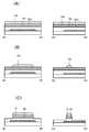
본 실시형태에 기재된 트랜지스터(10)의 변형예는 도 5(A)~5(C) 및 도 6(A)~6(C)를 참조하여 설명된다. 본 실시형태에 기재된 트랜지스터(10)는 단층 산화물 반도체막을 포함하고; 반대로, 본 변형예에 기재된 트랜지스터(10a) 및 트랜지스터(10b)는 각각 다층막을 포함한다.Modifications of the
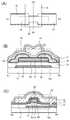
도 5(A)~5(C)는 반도체 장치에 포함되는 트랜지스터(10a)의 상면도 및 단면도이다. 도 5(A)는 트랜지스터(10a)의 상면도이고, 도 5(B)는 도 5(A)의 일점쇄선 A1-A2를 따라 취해진 단면도이며, 도 5(C)는 도 5(A)의 일점쇄선 A3-A4를 따라 취해진 단면도이다. 도 5(A)~5(C)에 있어서, 이해하기 쉽게 하기 위해서 몇몇 구성 요소가 확대, 크기 감소, 또는 생략된다.5A to 5C are a top view and a cross-sectional view of the
도 5(A)~5(C)에 도시된 트랜지스터(10a)는 산화물 반도체막(14) 대신에 다층막(24)이 제공된다는 점에서 트랜지스터(10)와 다르다.The
본 실시형태에 기재된 트랜지스터(10a)에 있어서, 다층막(24)은 산화물 반도체막(14) 및 산화물 반도체막(25)을 포함한다. 즉, 다층막(24)은 2층 구조를 갖는다. 또한, 산화물 반도체막(14)의 일부는 채널 영역으로서 기능한다.In the
산화물 반도체막(25)은 산화물 반도체막(14)을 형성하는 하나 이상의 원소를 함유한다. 따라서, 산화물 반도체막(14)과 산화물 반도체막(25) 사이의 계면에서 계면 산란이 일어나기 어렵다. 따라서, 캐리어의 이동이 계면에서 방해되지 않기 때문에 트랜지스터는 높은 전계 효과 이동도를 가질 수 있다.The
산화물 반도체막(25)은 적어도 In 또는 Zn을 함유하는 금속 산화물을 사용하여 형성된다. 금속 산화물의 대표예로는 In-Ga 산화물, In-Zn 산화물, In-Mg 산화물, Zn-Mg 산화물, 및 In-M-Zn 산화물(M은 Al, Ga, Sn, Y, Zr, La, Ce, Mg, 또는 Nd를 나타냄)을 포함한다. 산화물 반도체막(25)의 전도대 하단은 산화물 반도체막(14)의 것보다 진공 준위에 근접하고; 대표예로서, 산화물 반도체막(25)의 전도대 하단과 산화물 반도체막(14)의 전도대 하단 사이에 에너지 차는 0.05 eV 이상, 0.07 eV 이상, 0.1 eV 이상, 또는 0.15 eV 이상 중 어느 하나이고, 2 eV 이하, 1 eV 이하, 0.5 eV 이하, 또는 0.4 eV 이하 중 어느 하나이다. 즉, 산화물 반도체막(25)의 전자 친화도와 산화물 반도체막(14)의 전자 친화도 사이의 차는 0.05 eV 이상, 0.07 eV 이상, 0.1 eV 이상, 또는 0.15 eV 이상 중 어느 하나이고, 2 eV 이하, 1 eV 이하, 0.5 eV 이하, 또는 0.4 eV 이하 중 어느 하나이다.The
캐리어 이동도(전자 이동도)가 증가될 수 있기 때문에 산화물 반도체막(25)은 In을 함유하는 것이 바람직하다.Since the carrier mobility (electron mobility) can be increased, it is preferable that the
산화물 반도체막(25)이 원자비 중 In의 양보다 다량의 Al, Ga, Sn, Y, Zr, La, Ce, Mg, 또는 Nd를 함유하는 경우, 하기 효과 중 어느 하나가 얻어질 수 있다: (1) 산화물 반도체막(25)의 에너지 갭이 넓음; (2) 산화물 반도체막(25)의 전자 친화도가 감소; (3) 외부로부터 불순물 확산이 억제; (4) 산화물 반도체막(25)의 절연성이 산화물 반도체막(14)의 것과 비교해서 증가; 및 (5) Al, Ga, Sn, Y, Zr, La, Ce, Mg, 및 Nd가 산소와 강하게 결합되는 금속 원소이기 때문에 원자비 중 In의 양보다 원자비 중 다량의 Al, Ga, Sn, Y, Zr, La, Ce, Mg, 또는 Nd를 함유하는 산화물 반도체막(25)에서 산소 결손이 발생되기 어렵다.When the
산화물 반도체막(25)에 In-M-Zn 산화물을 사용하는 경우에 있어서, Zn 및 O를 고려하지 않은 경우, In의 비율 및 M의 비율은 각각 바람직하게 50 원자% 미만 및 50 원자% 이상이고, 각각 보다 바람직하게 25 원자% 미만 및 75 원자% 이상이다.In the case where In-M-Zn oxide is used for the
또한, 각각의 산화물 반도체막(14, 25)이 In-M-Zn 산화물(M은 Al, Ga, Sn, Y, Zr, La, Ce, Mg, 또는 Nd를 나타냄)을 함유하는 경우에 있어서, 산화물 반도체막(25)에서 M원자의 비율은 산화물 반도체막(14)의 것보다 높다. 대표예로서, 산화물 반도체막(25)에서 M의 비율은 산화물 반도체막(14)의 것만큼 높은 1.5배 이상, 바람직하게 2배 이상, 및 보다 바람직하게 3배 이상이다.In the case where each of the
또한, 각각의 산화물 반도체막(14, 25)이 In-M-Zn 산화물(M은 Al, Ga, Sn, Y, Zr, La, Ce, Mg, 또는 Nd를 나타냄)을 함유하는 경우에 있어서, In:M:Zn=x1:y1:z1[원자비]가 산화물 반도체막(25)에 만족되고 In:M:Zn=x2:y2:z2[원자비]가 산화물 반도체막(14)에 만족되는 경우, y1/x1은 y2/x2보다 높고, 바람직하게 y1/x1이 y2/x2만큼 높은 1.5배 이상이다. 또한, y1/x1은 y2/x2만큼 높은 2배 이상이 바람직하다. 또한, y1/x1은 y2/x2만큼 높은 3배 이상이 바람직하다. 이 경우에 있어서, 산화물 반도체막에 있어서, 산화물 반도체막을 포함하는 트랜지스터가 안정한 전기 특성을 가질 수 있기 때문에 y2가 x2 이상인 것이 바람직하다. 그러나, y2가 x2만큼 큰 3배 이상인 경우, 산화물 반도체막을 포함하는 트랜지스터의 전계 효과 이동도는 감소되고; 따라서, y2가 x2의 3배 미만인 것이 바람직하다.In the case where each of the
산화물 반도체막(14)이 In-M-Zn 산화물(M은 Al, Ga, Sn, Y, Zr, La, Ce, Mg, 또는 Nd를 나타냄)을 함유하고 In:M:Zn=x1:y1:z1의 금속 원소의 원자비를 갖는 타겟이 산화물 반도체막(14)을 형성하기 위해 사용되는 경우에 있어서, x1/y1은 바람직하게 1/3 이상 및 6 이하, 더욱 바람직하게 1 이상 및 6 이하이고, z1/y1은 바람직하게 1/3 이상 및 6 이하, 더욱 바람직하게 1 이상 및 6 이하이다. 또한, z1/y1가 1 이상 및 6 이하인 경우, 산화물 반도체막(14)으로서 후술되는 CAAC-OS막이 용이하게 형성된다. 타겟의 금속 원소의 원자비의 대표예로는 In:M:Zn=1:1:1, In:M:Zn=1:1:1.2, 및 In:M:Zn=3:1:2이다.The
산화물 반도체막(25)이 In-M-Zn 산화물(M은 Al, Ga, Y, Zr, La, Ce, Mg, 또는 Nd를 나타냄)을 함유하고 In:M:Zn=x2:y2:z2의 금속 원소의 원자비를 갖는 타겟이 산화물 반도체막(25)을 형성하기 위해 사용되는 경우에 있어서, x2/y2은 x1/y1 미만인 것이 바람직하고, z2/y2은 1/3 이상 및 6 이하가 바람직하며, 1 이상 및 6 이하가 더욱 바람직하다. 또한, z2/y2가 1 이상 및 6 이하인 경우, 산화물 반도체막(25)으로서 후술되는 CAAC-OS막이 용이하게 형성된다. 타겟의 금속 원소의 원자비의 대표예로는 In:M:Zn=1:3:2, In:M:Zn=1:3:4, In:M:Zn=1:3:6, In:M:Zn=1:3:8 등이다.Oxide semiconductor film (25) contains a (representing the M is Al, Ga, Y, Zr, La, Ce, Mg, or Nd) In-M-Zn oxide, andIn: M: Zn = x 2 : y 2: it is preferable that x2 / y2 is less than x1 / y1 , and z2 / y2 is less than x1 / y2 when the target having the atomic ratio of the metal element of z2 is used to form the
또한, 각각의 산화물 반도체막(14, 25)의 원자비의 각 금속 원소의 비율은 오차로서 상기 원자비의 것의 ±40% 범위 내로 달라진다.The ratio of each metal element in the atomic ratios of the
산화물 반도체막(25)의 두께는 3 ㎚ 이상 및 100 ㎚ 이하, 바람직하게 3 ㎚ 이상 및 50 ㎚ 이하이다.The thickness of the
산화물 반도체막(25)은, 예를 들면 산화물 반도체막(14)과 같은 비단결정 구조를 가질 수 있다. 비단결정 구조는, 예를 들면 후술되는 CAAC-OS, 다결정질 구조, 후술되는 미정질 구조, 또는 비정질 구조를 포함한다.The
산화물 반도체막(25)은, 예를 들면 비정질 구조를 가질 수 있다. 비정질 산화물 반도체막은, 예를 들면 원자 배열이 무질서하고 결정 성분을 갖지 않는다. 또한, 비정질 산화물 반도체막은, 예를 들면 완전한 비정질 구조이고 결정부를 갖지 않는다.The
또한, 산화물 반도체막(14, 25)은 각각 하기: 비정질 구조를 갖는 영역, 미정질 구조를 갖는 영역, 다결정질 구조를 갖는 영역, CAAC-OS의 영역, 및 단결정 구조를 갖는 영역 중 2개 이상을 포함하는 혼합막일 수 있다. 혼합막은, 예를 들면 비정질 구조를 갖는 영역, 미정질 구조를 갖는 영역, 다결정질 구조를 갖는 영역, CAAC-OS 영역, 및 단결정 구조를 갖는 영역 중 2개 이상을 포함하는 경우가 있다. 또한, 혼합막은 비정질 구조를 갖는 영역, 미정질 구조를 갖는 영역, 다결정질 구조를 갖는 영역, CAAC-OS 영역, 및 단결정 구조를 갖는 영역 중 2개 이상의 적층 구조를 갖는 경우가 있다.In addition, the
이 경우에 있어서, 산화물 반도체막(25)은 산화물 반도체막(14)과 게이트 절연막(17) 사이에 제공된다. 따라서, 트랩 준위가 불순물 및 결함에 의해 산화물 반도체막(25)과 게이트 절연막(17) 사이의 영역에 형성되면, 산화물 반도체막(14)과 영역 사이의 거리가 있기 때문에 산화물 반도체막(14)에 흐르는 전자는 트랩 준위에 의해 트랩되기 어려워진다. 따라서, 트랜지스터의 온-상태 전류량이 증가될 수 있고, 전계 효과 이동도가 증가될 수 있다. 전자가 트랩 준위에 의해 트랩되는 경우, 전자는 음의 고정된 전하가 된다. 결과적으로, 트랜지스터의 임계 전압이 달라진다. 그러나, 산화물 반도체막(14)과 영역 사이의 거리에 의해 트랩 준위에 의한 전자의 트랩이 감소될 수 있고, 따라서 임계 전압의 변동이 감소될 수 있다.In this case, the
산화물 반도체막(25)은 외부로부터 불순물을 차단할 수 있고, 따라서 외부에서 산화물 반도체막(14)으로 이송되는 불순물의 양을 감소시킬 수 있다. 또한, 산소 결손이 산화물 반도체막(25)에 형성되기 어려워진다. 결과적으로, 산화물 반도체막(14)의 불순물 밀도 및 산소 결손수는 감소될 수 있다.The
또한, 산화물 반도체막(14, 25)은 각각의 막을 단순하게 적층함으로써 형성되는 것이 아니고 연속 접합(여기서, 특히 전도대 하단이 각각의 막 사이에 연속적으로 변화되는 구조)을 형성하기 위해 형성된다. 즉, 각각의 계면에서 트랩 중심 또는 재결합 중심과 같은 결합 준위를 형성하는 불순물이 존재하지 않는 적층 구조가 제공된다. 적층되는 산화물 반도체막(14, 25) 사이에 불순물이 존재하는 경우, 에너지 밴드의 연속성이 손상되고, 캐리어가 계면에서 트랩되거나 재조합된 다음 사라지게 된다.Further, the
이러한 연속적인 에너지 밴드를 형성하기 위해서, 로드 록실(load lock chamber)을 포함하는 다중실 증착 장치(스퍼터링 장치)를 사용하여 대기에 노출되는 것 없이 연속적으로 막을 형성할 필요가 있다. 스퍼터링 장치에서 각 실은 산화물 반도체막에 대하여 불순물로서 기능하는 물 등을 가능한 한 많이 제거하기 위해서 크라이오 펌프와 같은 흡착 진공 배기 펌프를 사용해서 고진공 상태(약 5×10⁻⁷ ㎩~1×10⁻⁴ ㎩ 정도까지)가 되도록 배기되는 것이 바람직하다. 또한, 터보 분자 펌프 및 골드 트랩은 가스, 특히 배기계에서 실 내부로 탄소 또는 수소를 함유하는 가스의 역류를 방지하도록 조합되는 것이 바람직하다.In order to form such a continuous energy band, it is necessary to continuously form a film without exposure to the atmosphere by using a multi-chamber deposition apparatus (sputtering apparatus) including a load lock chamber. In the sputtering device, each chamber by using suction vacuum exhaust pump such as a cryo pump in order to remove as much as possible, such as water that acts as a dopant for the oxide semiconductor film high vacuum conditions (about5 × 10 -7 ㎩ ~ 1 × 10 -4 Pa or so). It is also preferred that the turbo-molecular pump and the gold trap are combined to prevent back flow of gases, especially gases containing carbon or hydrogen into the chamber from the exhaust system.
또한, 도 6(A)에 도시되는 트랜지스터(10b)의 다층막(34)은 다층막(24) 대신에 포함될 수 있다.In addition, the
산화물 반도체막(26), 산화물 반도체막(14), 및 산화물 반도체막(25)은 순서대로 다층막(34)에 적층된다. 즉, 다층막(34)은 3층 구조를 갖는다. 또한, 산화물 반도체막(14)은 채널 영역으로서 기능한다.The
또한, 베이스 절연막(13)은 산화물 반도체막(26)과 접하고 있다. 이것은 산화물 반도체막(26)이 베이스 절연막(13)과 산화물 반도체막(14) 사이에 제공되는 것을 의미한다.The
게이트 절연막(17)은 산화물 반도체막(25)과 접하고 있다. 즉, 산화물 반도체막(25)은 게이트 절연막(17)과 산화물 반도체막(14) 사이에 제공된다.The
산화물 반도체막(26)은 산화물 반도체막(25)의 것과 유사한 재료 및 형성방법을 사용하여 형성될 수 있다.The
산화물 반도체막(26)의 두께는 산화물 반도체막(14)의 것보다 작은 것이 바람직하다. 산화물 반도체막(26)의 두께가 1 ㎚ 이상 및 5 ㎚ 이하, 바람직하게 1 ㎚ 이상 및 3 ㎚ 이하인 경우, 트랜지스터의 임계 전압의 변동이 감소될 수 있다.It is preferable that the thickness of the
본 실시형태에 기재된 트랜지스터에서, 산화물 반도체막(26)은 산화물 반도체막(14)과 베이스 절연막(13) 사이에 제공된다. 따라서, 불순물 및 결함에 의해 산화물 반도체막(26)과 베이스 절연막(13) 사이의 영역에 트랩 준위가 형성되는 경우, 산화물 반도체막(14)과 영역 사이의 거리가 있기 때문에 산화물 반도체막(14)에 흐르는 전자는 트랩 준위에 의해 트랩되기 어려워진다. 따라서, 트랜지스터의 온-상태 전류량이 증가될 수 있고, 전계 효과 이동도가 증가될 수 있다. 전자가 트랩 준위에 의해 트랩되는 경우, 전자는 음의 고정된 전하가 된다. 결과적으로, 트랜지스터의 임계 전압이 달라진다. 그러나, 산화물 반도체막(14)과 영역 사이의 거리에 의해 트랩 준위에 의한 전자의 트랩이 감소될 수 있고, 따라서 임계 전압의 변동이 감소될 수 있다.In the transistor described in this embodiment mode, the
산화물 반도체막(26)은 외부로부터 불순물의 침입을 차단할 수 있고, 따라서 외부로부터 산화물 반도체막(14)에 이송되는 불순물의 양이 감소될 수 있다. 또한, 산소 결손은 산화물 반도체막(26)에 형성되기 어려워진다. 결과적으로, 산화물 반도체막(14)의 불순물 농도 및 산소 결손수는 감소될 수 있다.The
산화물 반도체막(25)은 게이트 절연막(17)과 산화물 반도체막(14) 사이에 제공되고, 산화물 반도체막(26)은 산화물 반도체막(14)과 베이스 절연막(13) 사이에 제공된다. 따라서, 산화물 반도체막(25)과 산화물 반도체막(14) 사이의 계면 근방에서, 산화물 반도체막(14)에서, 또는 산화물 반도체막(26)과 산화물 반도체막(14) 사이의 계면 근방에서 실리콘 또는 탄소의 농도를 감소시키는 것이 가능해진다.The
이러한 구조를 갖는 트랜지스터(10b)는 산화물 반도체막(14)을 포함하는 다층막(34)의 매우 적은 결함을 포함하기 때문에 온-상태 전류 및 전계 효과 이동도에 의해 대표되는 이러한 트랜지스터의 전기 특성을 개선시킬 수 있다. 또한, 스트레스 시험의 예인 게이트 BT 스트레스 시험 및 게이트 BT 포토스트레스 시험에서 임계 전압의 변동이 작으므로, 신뢰도가 높다.Since the
도 6(B)에 도시된 트랜지스터(10c)의 경우와 같이, 도전막(12)이 제공되지 않은 구조를 채용할 수 있다.A structure in which the
또한, 도 6(C)에 도시된 트랜지스터(10d)의 구조를 채용할 수 있다.Further, the structure of the
<변형예 2>≪ Modification Example 2 &
본 실시형태에 기재된 트랜지스터(10)의 변형예는 도 7(A)~7(C)을 참조하여 설명된다. 본 변형예에 있어서, 산화물 반도체막이 게이트 절연막과 한 쌍의 전극 사이에 제공되는 트랜지스터가 설명된다.Modifications of the
도 7(A)~7(C)은 본 발명의 일 실시형태의 반도체 장치에 포함되는 트랜지스터(10e)의 상면도 및 단면도이다. 도 7(A)은 상면도이고, 도 7(B)은 도 7(A)의 일점쇄선 A1-A2를 따라 취해진 모식적인 단면도이며, 도 7(C)은 도 7(A)의 일점쇄선 A3-A4를 따라 취해진 모식적인 단면도이다. 도 7(A)~7(C)에 있어서, 이해를 용이하게 하기 위해서 몇몇 구성 요소를 확대, 크기 감소, 또는 생략한다.7A to 7C are a top view and a cross-sectional view of a
도 7(A)에 도시된 트랜지스터(10e)는 기판(11) 상에 도전막(12), 기판(11)과 도전막(12) 상에 베이스 절연막(13), 베이스 절연막(13) 상에 산화물 반도체막(26), 산화물 반도체막(26) 상에 산화물 반도체막(14), 베이스 절연막(13)과 산화물 반도체막(26) 상에 있고 산화물 반도체막(14)과 접하고 있는 산화 방지막(20), 산화 방지막(20) 상에 한 쌍의 전극(15, 16), 산화 방지막(20)과 한 쌍의 전극(15, 16)과 접하고 있는 산화물 반도체막(25), 산화물 반도체막(25) 상에 게이트 절연막(17), 및 게이트 절연막(17)을 통해서 산화물 반도체막(14)과 중첩하는 게이트 전극(18)을 포함한다. 절연막(19)은 게이트 절연막(17)과 게이트 전극(18) 상에 형성될 수 있다.The
도 7(B)에 도시된 바와 같이, 산화물 반도체막(25)은 산화 방지막(20)의 상면 및 한 쌍의 전극(15, 16)의 상면 및 측면과 접하고 있다. 도 7(C)에 도시된 바와 같이, 산화물 반도체막(25)은 베이스 절연막(13) 상면의 일부와 접하고 있다.7 (B), the
도 7(C)에 도시된 바와 같이, 트랜지스터(10e)의 채널 폭 방향에서 게이트 전극(18)은 게이트 절연막(17)을 통해서 산화물 반도체막(14) 및 산화물 반도체막(26) 상면 및 측면과 면하고 있다.The
게이트 전극(18)은 산화물 반도체막(14)을 전기적으로 둘러싸고 있다. 이 구조를 사용하여 트랜지스터(10e)의 온-상태 전류가 증가될 수 있다. 이러한 트랜지스터 구조를 둘러싸인 채널(s-채널) 구조라 불린다. 또한, s-채널 구조에서, 전류는 산화물 반도체막(14)의 전체(벌크)에 흐른다. 산화물 반도체막(14)의 내부에 전류가 흐르기 때문에, 전류는 계면 산란에 의해 거의 영향을 받지 않고, 높은 온-상태 전류가 얻어질 수 있다. 또한, 산화물 반도체막(14)을 두껍게 제조함으로써 온-상태 전류가 증가될 수 있다.The
작은 채널 길이 및 작은 채널 폭을 가진 트랜지스터를 제조할 때, 레지스트 마스크를 크기 감소시키면서 한 쌍의 전극, 산화물 반도체막 등이 가공되는 경우, 한 쌍의 전극, 산화물 반도체막 등은 둥근 단부(곡면)를 갖는 경우가 있다. 이 구조를 사용하여 산화물 반도체막(14) 상에 형성되는 산화물 반도체막(25) 및 게이트 절연막(17)과의 피복성을 개선시킬 수 있다. 또한, 한 쌍의 전극(15, 16)의 단부에서 일어날 수 있는 전계 집중을 완화시킬 수 있고, 이것은 트랜지스터의 열화를 억제시킬 수 있다.When manufacturing a transistor having a small channel length and a small channel width, when a pair of electrodes, an oxide semiconductor film or the like is processed while reducing the size of the resist mask, the pair of electrodes, the oxide semiconductor film, . By using this structure, the coverage with the
또한, 트랜지스터를 소형화함으로써 높은 직접도와 높은 밀도를 달성할 수 있다. 예를 들면, 트랜지스터의 채널 길이는 100 ㎚ 이하, 바람직하게 40 ㎚ 이하, 더욱 바람직하게 30 ㎚ 이하, 가장 바람직하게 20 ㎚ 이하로 설정되고, 트랜지스터의 채널 폭은 100 ㎚ 이하, 바람직하게 40 ㎚ 이하, 더욱 바람직하게 30 ㎚ 이하, 가장 바람직하게 20 ㎚ 이하로 설정된다. 상술한 바와 같이 그것의 채널 폭이 단축되는 경우라도 s-채널 구조를 가진 본 발명의 일 실시형태의 트랜지스터는 온-상태 전류를 증가시킬 수 있다.In addition, high directivity and high density can be achieved by miniaturizing the transistor. For example, the channel length of the transistor is set to 100 nm or less, preferably 40 nm or less, more preferably 30 nm or less, most preferably 20 nm or less, and the channel width of the transistor is 100 nm or less, preferably 40 nm or less , More preferably 30 nm or less, and most preferably 20 nm or less. The transistor of the embodiment of the present invention having the s-channel structure can increase the on-state current even if its channel width is shortened as described above.
반도체 장치의 높은 직접도는 트랜지스터의 소형화를 요구한다. 그러나, 트랜지스터의 소형화는 트랜지스터의 전기 특성의 열화를 야기한다는 것으로 알려져 있다. 채널 폭의 감소는 온-상태 전류의 감소를 야기한다.The high degree of directivity of the semiconductor device requires the miniaturization of the transistor. However, it is known that the miniaturization of the transistor causes deterioration of the electric characteristics of the transistor. A decrease in channel width causes a decrease in on-state current.
그러나, 본 발명의 일 실시형태의 트랜지스터에서, 상술한 바와 같이 산화물 반도체막(25)은 산화물 반도체막(14)의 채널 형성 영역을 덮기 위해 형성되고, 채널 형성 영역 및 게이트 절연막(17)은 서로 접하고 있지 않다. 따라서, 산화물 반도체막(14)과 게이트 절연막(17) 사이의 계면에 형성되는 캐리어의 산란은 억제될 수 있음으로써 트랜지스터의 온 상태 전류가 증가될 수 있다.However, in the transistor of the embodiment of the present invention, as described above, the
산화물 반도체막이 진성 또는 실질적 진성으로 제조되는 경우에 있어서, 산화물 반도체막에 함유되는 캐리어 수의 감소는 전계 효과 이동도를 감소시킬 수 있다. 그러나, 본 발명의 일 실시형태의 트랜지스터에서, 산화물 반도체막(14)에 수직 방향뿐만 아니라 측면으로도 게이트 전계가 적용된다. 즉, 게이트 전계가 산화물 반도체막(14)의 전체에 적용됨으로써 산화물 반도체막의 벌크에 전류가 흐른다. 고순도 진성 특성에 의해 전기 특성의 변화가 감소되면서 트랜지스터의 전계 효과 이동도를 개선시키는 것이 가능해진다.In the case where the oxide semiconductor film is produced with intrinsic or substantial intrinsic properties, the reduction in the number of carriers contained in the oxide semiconductor film can reduce the field effect mobility. However, in the transistor of the embodiment of the present invention, the gate electric field is applied not only to the vertical direction but also to the side surface of the
본 발명의 일 실시형태의 트랜지스터에서, 산화물 반도체막(14)은 산화물 반도체막(26) 상에 형성되어 계면 상태가 형성되기 어려워진다. 또한, 산화물 반도체막(14)이 산화물 반도체막(25, 26) 사이에 제공되기 때문에 불순물이 상하로부터 산화물 반도체막(14)에 침입하지 않는다. 따라서, 산화물 반도체막(14)은 산화물 반도체막(26)과 산화물 반도체막(25)에 의해 둘러싸여 있어(게이트 전극(18)에 의해 전기적으로도 둘러싸임), 상술한 트랜지스터의 온-상태 전류의 개선에 더해서 임계 전압의 안정성이 가능해진다. 결과적으로, 게이트 전극의 전압이 0V인 경우 소스와 드레인 사이에 흐르는 전류는 감소될 수 있고, 이것은 낮은 전력 소비를 이끈다. 또한, 트랜지스터의 임계 전압이 안정해지므로, 반도체 장치의 장기간 신뢰도가 개선될 수 있다.In the transistor of the embodiment of the present invention, the
또한, 본 실시형태에 기재된 구조, 방법 등은 다른 실시형태 및 실시예에 기재된 구조, 방법 등 중 어느 하나와 적절하게 조합해서 사용될 수 있다.The structures, methods, and the like described in this embodiment can be used in appropriate combination with any of structures, methods, and the like described in other embodiments and examples.
<트랜지스터의 밴드 구조><Band Structure of Transistor>
이어서, 도 5(A)~5(C)에 도시된 트랜지스터(10a)에 포함되는 다층막(24) 및 도 6(A)에 도시된 트랜지스터(10b)에 포함되는 다층막(34)의 밴드 구조를 도 8(A)~8(D)을 참조해서 설명할 것이다.Next, the band structure of the
여기서, 3.15 eV의 에너지 갭을 갖는 In-Ga-Zn 산화물은 산화물 반도체막(14)에 사용되고, 3.5 eV의 에너지 갭을 갖는 In-Ga-Zn 산화물은 산화물 반도체막(25)에 사용된다. 에너지 갭은 분광 엘립소미터(HORIBA JOBIN YVON SAS.사 UT-300)를 사용하여 측정된다.Here, an In-Ga-Zn oxide having an energy gap of 3.15 eV is used for the
산화물 반도체막(14)의 진공 준위와 가전자대 상단 사이의 에너지 차(이온화 전위라고도 불림) 및 산화물 반도체막(25)의 진공 준위와 가전자대 상단 사이의 에너지 차는 각각 8 eV 및 8.2 eV이다. 또한, 진공 준위와 가전자대 상단 사이의 에너지 차는 자외광 전자분광법(UPS) 장치(ULVAC-PHI, Inc.사 VersaProbe)를 사용하여 측정된다.The energy difference between the vacuum level of the
따라서, 산화물 반도체막(14)의 진공 준위와 전도대 하단 사이의 에너지 차(전자 친화력이라고도 불림) 및 산화물 반도체막(25)의 진공 준위와 전도대 하단 사이의 에너지 차는 각각 4.85 eV 및 4.7 eV이다.Therefore, the energy difference between the vacuum level of the
도 8(A)은 트랜지스터(10a)에 포함되는 다층막(24)의 밴드 구조의 일부를 모식적으로 도시한다. 여기서, 산화 실리콘막이 베이스 절연막(13) 및 게이트 절연막(17)에 사용되고 산화 실리콘막이 다층막(24)과 접하여 제공되는 경우에 대해서 설명한다. 도 8(A)에 있어서, EcI1은 산화 실리콘막의 전도대 하단을 나타내고; EcS1은 산화물 반도체막(14)의 전도대 하단을 나타내며; EcS2는 산화물 반도체막(25)의 전도대 하단을 나타내고; EcI2는 산화 실리콘막의 전도대 하단을 나타낸다. 또한, EcI1 및 EcI2는 각각 도 5(B)의 베이스 절연막(13) 및 게이트 절연막(17)과 대응된다.8A schematically shows a part of the band structure of the
도 8(A)에 도시된 바와 같이, 산화물 반도체막(14, 25) 사이에 전도대 하단이 서서히 변화된다. 즉, 전도대 하단이 연속적으로 변화된다. 이것은 다층막(24)이 산화물 반도체막(14)에 함유되는 원소를 함유하고 산소가 산화물 반도체막(14, 25) 사이에 이송되어 혼합층이 형성되기 때문이다.The lower end of the conduction band is gradually changed between the
도 8(A)에 나타낸 바와 같이, 다층막(24)의 산화물 반도체막(14)은 우물(well)로서 기능하고 다층막(24)을 포함하는 트랜지스터의 채널 영역은 산화물 반도체막(14)에 형성된다. 또한, 다층막(24)의 전도대 하단이 연속적으로 변화하기 때문에, 산화물 반도체막(14, 25) 사이에 연속 접합이 형성된다고 말할 수 있다.The
도 8(A)에 나타낸 바와 같이, 산화물 반도체막(25)과 게이트 절연막(17) 사이에 계면 근방에서 불순물 또는 결함으로 인한 트랩 준위가 발생될 수 있지만, 트랩 준위가 산화물 반도체막(25)의 존재로 인해 발생되는 영역으로부터 산화물 반도체막(14)이 떨어져 있다. 그러나, EcS1과 EcS2 사이의 에너지 차가 작을 경우, 산화물 반도체막(14)의 전자는 에너지 차를 지나 트랩 준위에 도달할 수 있다. 전자가 트랩 준위에 의해 트랩되는 경우, 음의 고정된 전하가 게이트 절연막과의 계면에 발생됨으로써 트랜지스터의 임계 전압이 양의 방향으로 시프트한다. 따라서, 트랜지스터의 임계 전압의 변화가 감소되고 안정한 전기 특성이 얻어지기 때문에 EcS1와 EcS2 사이의 에너지 차는 0.1 eV 이상, 더욱 바람직하게는 0.15 eV 이상인 것이 바람직하다.A trap level due to impurities or defects may be generated in the vicinity of the interface between the
도 8(B)은 트랜지스터(10a)의 다층막(24)의 밴드 구조의 일부를 모식적으로 도시하고, 이것은 도 8(A)에 나타낸 밴드 구조의 변화이다. 여기서, 산화 실리콘막이 베이스 절연막(13)과 게이트 절연막(17)에 사용되고 산화 실리콘막이 다층막(24)과 접하고 있는 구조에 대해서 설명한다. 도 8(B)에 있어서, EcI1은 산화 실리콘막의 전도대 하단을 나타내고; EcS1은 산화물 반도체막(14)의 전도대 하단을 나타내며; EcI2는 산화 실리콘막의 전도대 하단을 나타낸다. 또한, EcI1 및 EcI2는 각각 도 5(B)의 베이스 절연막(13)과 게이트 절연막(17)과 대응된다.8B schematically shows a part of the band structure of the
도 5(B)에 도시된 트랜지스터에 있어서, 다층막(24)의 상부, 즉 산화물 반도체막(25)은 한 쌍의 전극(15, 16) 형성 시에 에칭될 수 있다. 또한, 산화물 반도체막(14)의 혼합층은 산화물 반도체막(25) 형성시의 산화물 반도체막(14)의 상면에 형성되기 쉽다.In the transistor shown in Fig. 5 (B), the upper portion of the
예를 들면, 산화물 반도체막(14)이 스퍼터링 타겟으로서 In~Ga 및 Zn의 원자비가 1:1:1 또는 3:1:2인 In-Ga-Zn 산화물의 사용으로 형성되는 산화물 반도체막이고, 산화물 반도체막(25)이 스퍼터링 타겟으로서 In~Ga 및 Zn의 원자비가 1:3:2, 1:3:4, 1:3:6, 또는 1:4:5인 In-Ga-Zn 산화물의 사용으로 형성되는 산화물막인 경우에 있어서, 산화물 반도체막(25) 중 Ga 함량은 산화물 반도체막(14)의 것보다 높다. 따라서, Ga 함량이 산화물 반도체막(14)의 것보다 높은 GaOx층 또는 혼합층이 산화물 반도체막(14)의 상면에 형성될 수 있다.For example, the
그 이유로 인해, 산화물 반도체막(25)이 에칭되는 경우라도 EcI2측에 대한 전도대 하단 EcS1은 증가되고, 도 8(B)에 나타낸 밴드 구조가 얻어질 수 있는 경우가 있다.For this reason, even when the
도 8(B)에 나타낸 밴드 구조의 경우와 같이, 채널 영역 단면의 관찰시에 다층막(24)의 산화물 반도체막(14)만 명확하게 관찰되는 경우가 있다. 그러나, 실제로 산화물 반도체막(14)보다 많은 Ga를 함유하는 혼합층을 산화물 반도체막(14) 상에 형성함으로써, 혼합층이 1.5번째 층으로서 여겨질 수 있다. 또한, 혼합층은, 예를 들면 EDX 분석에 의해 다층막(24)에 함유되는 원소가 측정되는 경우 산화물 반도체막(14)의 상부 조성을 분석함으로써 확인될 수 있다. 혼합층은, 예를 들면 산화물 반도체막(14)의 상부 조성의 Ga 함량이 산화물 반도체막(14)의 Ga 함량보다 큰 방식으로 확인될 수 있다.Only the
도 8(C)은 트랜지스터(10b)의 다층막(34)의 밴드 구조의 일부를 모식적으로 도시한다. 여기서, 산화 실리콘막이 베이스 절연막(13)과 게이트 절연막(17)에 사용되고 산화 실리콘막이 다층막(34)과 접하고 있는 경우에 대해서 설명한다. 도 8(C)에 있어서, EcI1은 산화 실리콘막의 전도대 하단을 나타내고; EcS1은 산화물 반도체막(14)의 전도대 하단을 나타내며; EcS2는 산화물 반도체막(25)의 전도대 하단을 나타내고; EcS3은 산화물 반도체막(26)의 전도대 하단을 나타내며; EcI2는 산화 실리콘막의 전도대 하단을 나타낸다. 또한, EcI1 및 EcI2는 각각 도 6(A)의 베이스 절연막(13) 및 게이트 절연막(17)과 대응된다.8 (C) schematically shows a part of the band structure of the
도 8(C)에 도시된 바와 같이, 산화물 반도체막(26, 14, 25) 사이의 에너지 배리어가 존재하지 않고, 그것의 전도대 하단은 완만하게 달라진다. 즉, 전도대 하단은 연속적이다. 이것은 산화물 반도체막(14)에 함유되는 원소를 다층막(34)이 함유하고 산화물 반도체막(14, 26) 사이 및 산화물 반도체막(14, 25) 사이에 산소가 이송되어 혼합층을 형성하기 때문이다.As shown in Fig. 8 (C), there is no energy barrier between the
도 8(C)에 나타낸 바와 같이, 다층막(34)의 산화물 반도체막(14)은 우물(well)로서 기능하고 다층막(34)을 포함하는 트랜지스터의 채널 영역은 산화물 반도체막(14)에 형성된다. 또한, 다층막(34)의 전도대 하단이 연속적으로 변화하기 때문에, 그것은 상기 연속 접합이 산화물 반도체막(26, 14) 사이 및 산화물 반도체막(25, 14) 사이에 형성될 수 있다.The
불순물 또는 결함으로 인해 트랩 준위가 산화물 반도체막(14)과 게이트 절연막(17) 사이의 근방 및 산화물 반도체막(14)과 베이스 절연막(13) 사이의 계면 근방에서 발생될 수 있지만, 도 8(C)에 도시된 바와 같이 산화물 반도체막(25, 26)의 존재로 인해 트랩 준위가 발생되는 영역으로부터 산화물 반도체막(14)이 떨어져 있을 수 있다. 그러나, EcS1과 EcS2 사이의 에너지 차 및 EcS1과 EcS3 사이의 에너지 차가 작은 경우, 산화물 반도체막(14)의 전자는 에너지 차를 지나 트랩 준위에 도달할 수 있다. 전자가 트랩 준위에 의해 트랩되는 경우, 음의 고정된 전하가 절연막과의 계면에서 발생됨으로써 트랜지스터의 임계 전압은 양의 방향으로 시프트된다. 따라서, 트랜지스터의 임계 전압의 변화가 감소되고 안정한 전기 특성이 얻어지기 때문에, EcS1과 EcS2 사이의 에너지 차 및 EcS1과 EcS3 사이의 에너지 차는 0.1 eV 이상, 더욱 바람직하게는 0.15 eV 이상인 것이 바람직하다.The trap level can be generated in the vicinity of the interface between the
산화물 반도체막(27)은 산화물 반도체막(25)과 게이트 절연막(17) 사이에 제공될 수 있다. 산화물 반도체막(27)이 산화물 반도체막(25)보다 낮은 전자 친화력을 가지도록 산화물 반도체막(27)의 재료가 선택된다. 산화물 반도체막(27)의 재료에 대해서, 산화물 반도체막(14), 산화물 반도체막(25), 산화물 반도체막(26) 등의 재료를 나타낸다. 도 8(D)은 이러한 다층막의 밴드 구조를 나타낸다. 또한, EcS4는 산화물 반도체막(27)의 전도대 하단을 나타낸다.The
또한, 트랜지스터의 구조는 상기 구조에 제한되지 않는다. 도 9(A)의 도시된 트랜지스터가 형성되도록 한 쌍의 전극(15, 16)을 마스크로서 사용하여 산화 방지막(20)을 형성하거나, 도 9(B)의 도시된 트랜지스터가 형성되도록 한 쌍의 전극(15, 16) 및 레지스트를 마스크로서 사용하여 산화 방지막(20)을 형성할 수 있다. 상술한 다층막 중 어느 하나를 포함하는 트랜지스터는 이러한 구조를 가질 수 있다.Further, the structure of the transistor is not limited to the above structure. The
도 10(A), 도 10(B), 또는 도 10(C)에 도시된 바와 같이, 상기 구조는 각각 오프셋 영역의 저항이 감소되는 자기 정렬된 구조일 수 있다.As shown in Fig. 10 (A), 10 (B), or 10 (C), the structure may be a self-aligned structure in which the resistance of the offset regions is reduced.
n형 저저항 영역(41) 및 n형 저저항 영역(42)은 마스크로서 게이트 전극(18)을 사용하여 불순물을 첨가함으로써 형성될 수 있다. 불순물을 첨가하기 위한 방법으로서, 이온 주입법, 이온 도핑법, 플라즈마 액침 이온 주입법 등이 사용될 수 있다.The n-type
수소, 헬륨, 네온, 아르곤, 크립톤, 크세논, 붕소, 질소, 인, 및 비소와 같은 불순물은 산화물 반도체막(14, 25, 26)의 도전성을 증가시킨다.Impurities such as hydrogen, helium, neon, argon, krypton, xenon, boron, nitrogen, phosphorus, and arsenic increase the conductivity of the
또한, 마스크로서 게이트 전극(18)을 사용하여 불순물을 첨가할 필요가 없다. 그 경우의 예를 도 11(A)~11(C)에 나타낸다. 게이트 전극(18)의 단부가 도 11(A)~11(C)의 한 쌍의 전극(15, 16)의 단부와 정렬되지 않지만, 본 발명의 일 실시형태는 그것에 제한되지 않고, 게이트 전극(18)의 단부는 한 쌍의 전극(15, 16)의 단부와 정렬될 수 있다.Further, it is not necessary to add the impurity using the
테이퍼드된 형상을 갖는 게이트 전극(18)으로 저저항 영역(41, 42)의 형상은 도 12(A)~12(C)에 도시된 바와 같이 제어될 수 있다.The shape of the
채널 등이 산화물 반도체막에 형성되는 예를 본 실시형태에 기재하지만, 본 발명의 일 실시형태는 그것에 제한되지 않는다. 예를 들면, 경우 또는 조건에 따라, 채널, 채널 근방, 소스 영역, 드레인 영역 등은 Si(실리콘), Ge(게르마늄), SiGe(실리콘 게르마늄), GaAs(갈륨 비소) 등을 함유하는 재료를 사용하여 형성될 수 있다.Channel or the like is formed in the oxide semiconductor film is described in the present embodiment, an embodiment of the present invention is not limited thereto. For example, a material containing Si (silicon), Ge (germanium), SiGe (silicon germanium), GaAs (gallium arsenide), or the like is used for a channel, a channel neighborhood, a source region, .
또한, 본 실시형태에 기재된 구조, 방법 등은 다른 실시형태 및 실시예에 기재된 구조, 방법 등의 어느 하나와 적절하게 조합하여 사용될 수 있다.The structures, methods, and the like described in this embodiment can be appropriately combined with any of structures, methods, and the like described in other embodiments and examples.
(실시형태 2)(Embodiment 2)
본 실시형태에 있어서, 실시형태 1에 기재된 트랜지스터의 구조와 다른 구조를 갖는 트랜지스터에 대해서 설명할 것이다.In the present embodiment, a transistor having a structure different from that of the transistor described in
<1. 트랜지스터의 구조><1. Transistor Structure>
도 13(A)~13(C)은 반도체 장치에 포함되는 트랜지스터(50)의 상면도 및 단면도이다. 도 13(A)은 트랜지스터(50)의 상면도이고, 도 13(B)은 도 13(A)의 일점쇄선 B1-B2를 따라 취해진 단면도이며, 도 13(C)은 도 13(A)의 일점쇄선 B3-B4를 따라 취해진 단면도이다. 도 13(A)~13(C)에 있어서, 이해하기 용이하게 하기 위해서 몇몇 구성 요소는 확대, 크기 감소, 또는 생략된다. 몇몇 경우에 있어서, 일점쇄선 B1-B2의 방향은 채널 길이 방향이라 불리고, 일점쇄선 B3-B4의 방향은 채널 폭 방향이라 불린다.13 (A) to 13 (C) are a top view and a cross-sectional view of the
도 13(A)~13(C)에 도시된 트랜지스터(50)는 기판(11) 상에 도전막(12), 기판(11)과 도전막(12) 상에 베이스 절연막(13), 베이스 절연막(13) 상에 산화물 반도체막(26), 산화물 반도체막(26) 상에 산화물 반도체막(14), 산화물 반도체막(14)의 상면에 한 쌍의 전극(15, 16), 산화물 반도체막(14) 및 한 쌍의 전극(15, 16)과 접하는 산화물 반도체막(25), 산화물 반도체막(25) 상에 게이트 절연막(17), 및 게이트 절연막(17)을 통해서 산화물 반도체막(14)과 중첩하는 게이트 전극(18)을 포함한다. 절연막(19)은 게이트 절연막(17)과 게이트 전극(18) 상에 형성될 수 있다.A
한 쌍의 전극(15, 16)이 산화물 반도체막(14)의 상면에만 형성되기 때문에, 베이스 절연막(13)으로부터 산소에 의해 유도되는 한 쌍의 전극(15, 16)의 산화가 억제될 수 있다. 산화물 반도체막(14)에 있어서, 한 쌍의 전극(15, 16)과 중첩하는 영역의 채널 폭은 한 쌍의 전극(15, 16)과 중첩하지 않는 영역(채널이 형성되는 영역)의 채널 폭보다 길다. 따라서, 한 쌍의 전극(15, 16)과 중첩하지 않는 영역의 채널 폭을 단축할 수 있고, 이것은 트랜지스터의 소형화를 이끌며, 산화물 반도체막(14)이 한 쌍의 전극(15, 16)과 접하고 있는 영역의 부분이 증가될 수 있고, 이것은 접촉 저항의 감소를 이끈다.Oxidation of the pair of
<2. 트랜지스터를 제조하기 위한 방법><2. Method for manufacturing a transistor>
이어서, 도 13(A)~13(C)의 트랜지스터(50)를 제조하기 위한 방법은 도 14(A)~14(C) 및 15(A)~15(C)를 참조하여 설명된다. 도 13(A)의 일점쇄선 B1-B2를 따르는 채널 길이 방향으로의 단면 및 도 13(A)의 일점쇄선 B3-B4를 따르는 채널 폭 방향으로의 단면은 도 14(A)~14(C) 및 도 15(A)~15(C)에 사용되어 트랜지스터(50)를 제조하기 위한 방법을 설명한다.Next, a method for manufacturing the
도 2(A)~2(C)의 단계 후, 산화물 반도체막(26a), 산화물 반도체막(14a), 및 도전막(15a)을 포함하는 적층은 베이스 절연막(13) 상에 형성된다(도 14(A) 참조). 산화물 반도체막(26a), 산화물 반도체막(14a), 및 도전막(15a)의 재료 및 형성방법을 실시형태 1에 나타낸다.After the steps of Figs. 2A to 2C, a lamination including the
그 다음, 도전막(15a)을 에칭하여 도전막(15b)을 형성한다(도 14(B) 참조).Then, the
이어서, 산화물 반도체막(26a) 및 산화물 반도체막(14a)을 마스크로서 도전막(15b)을 사용하여 에칭해서 산화물 반도체막(26) 및 산화물 반도체막(14)을 형성한다(도 14(C) 참조).14 (C), the
이어서, 도전막(15b)을 에칭하여 한 쌍의 전극(15, 16)을 형성한다(도 15(A) 참조).Then, the
그 다음, 산화물 반도체막(25) 및 게이트 절연막(17)을 산화물 반도체막(14) 및 한 쌍의 전극(15, 16) 상에 형성한다(도 15(B) 참조). 산화물 반도체막(25) 및 게이트 절연막(17)의 재료 및 형성방법을 실시형태 1에 나타낸다.The
그 후, 게이트 절연막(17)을 통해서 산화물 반도체막(14)과 중첩하는 게이트 전극(18)을 형성한다. 이어서, 절연막(19)을 게이트 절연막(17) 및 게이트 전극(18) 상에 형성한다(도 15(C) 참조). 게이트 전극(18) 및 절연막(19)의 재료 및 형성방법을 실시형태 1에 나타낸다.Thereafter, the
상기 단계를 통해서, 임계 전압의 시프트가 감소되는 트랜지스터가 제조될 수 있다. 또한, 전기 특성 변화가 감소되는 트랜지스터가 제조될 수 있다.Through this step, a transistor in which the shift of the threshold voltage is reduced can be manufactured. In addition, a transistor in which a change in electrical characteristics is reduced can be manufactured.
<변형예 1>≪ Modification Example 1 &
본 실시형태에 기재된 트랜지스터(50)의 변형예는 도 16(A)~16(C)을 참조하여 설명된다.A modification of the
도 16(A)에 도시된 트랜지스터(50a)는 산화물 반도체막(25)과 게이트 절연막(17)의 형상에 있어서 트랜지스터(50)와 다르다. 도 16(A)의 산화물 반도체막(25)과 게이트 절연막(17)이 마스크로서 게이트 전극(18)을 사용하여 형성되기 때문에 마스크 수가 감소될 수 있다.The
또한, 산화물 반도체막(25) 및 게이트 절연막(17)을 형성하기 위한 마스크 및 게이트 전극(18)을 형성하기 위한 마스크를 사용해서 도 16(B)에 도시된 트랜지스터(50b)가 형성될 수 있다.The
도 16(C)에 도시된 트랜지스터(50c)의 경우와 같이, 도전막(12)이 제공되지 않는 구조를 채용할 수 있다.A structure in which the
도 17(A)~17(C)에 도시된 트랜지스터(50d)는 한 쌍의 전극(15, 16)을 형성한 후에 산화물 반도체막(26, 14)을 형성함으로써 얻어지는 구조를 가질 수 있다.The
도 18(A)~18(C)에 도시된 바와 같이, 상기 구조는 각각 오프셋 영역의 저항이 감소되는 자기 정렬된 구조일 수 있다.As shown in Figures 18 (A) - 18 (C), the structure may be a self-aligned structure in which the resistance of the offset regions is reduced, respectively.
n형 저저항 영역(41, 42)은 마스크로서 게이트 전극(18)을 사용하여 불순물을 첨가함으로써 형성될 수 있다. 불순물 및 불순물을 첨가하기 위한 방법을 실시형태 1에 나타낸다.The n-type
또한, 마스크로서 게이트 전극(18)의 사용으로 불술물을 첨가할 필요는 없다. 그 경우의 예를 도 19(A)~19(C)에 나타낸다. 게이트 전극(18)의 단부가 도 19(A)~19(C)의 한 쌍의 전극(15, 16)의 단부와 정렬되지 않지만, 본 발명의 일 실시형태는 그것에 제한되지 않고, 게이트 전극(18)의 단부는 한 쌍의 전극(15, 16)의 단부와 정렬될 수 있다.Further, the use of the
도 12(A)~12(C)의 경우와 같이, 도 18(A)~18(C)의 게이트 전극(18)은 테이퍼드된 형상을 가질 수 있어 저저항 영역(41, 42)의 형상이 도 20(A)~20(C)에 도시된 바와 같이 제어될 수 있다.The
또한, 본 실시형태에 기재된 구조, 방법 등은 다른 실시형태 및 실시예에 기재된 구조, 방법 등의 어느 하나와 적절하게 조합해서 사용될 수 있다.The structures, methods, and the like described in this embodiment can be appropriately combined with any of structures, methods, and the like described in other embodiments and examples.
(실시형태 3)(Embodiment 3)
본 실시형태에 있어서, 트랜지스터에 포함되는 산화물 반도체막, 산화물 반도체막과 접하는 산화물 절연막(베이스 절연막 또는 게이트 절연막)에 포함되는 결함, 트랜지스터 특성의 열화에 대해서 설명한다.In the present embodiment, the deterioration of the transistor characteristics and defects contained in the oxide semiconductor film included in the transistor and the oxide insulating film (base insulating film or gate insulating film) in contact with the oxide semiconductor film will be described.
<1. NOx><1. NOx >
우선, 산화물 반도체막과 접하는 산화물 절연막에 함유되는 질소 산화물(이하, NOx; x는 0 초과 및 2 이하, 바람직하게 1 이상 및 2 이하임)에 대해서 설명한다.First, a description will be given of a nitrogen oxide (hereinafter, referred to as NOx (x is more than 0 and not more than 2, preferably not less than 1 and not more than 2) contained in an oxide insulating film in contact with the oxide semiconductor film.
<1-1. 산화물 절연막 중의 NOx의 전이 레벨><1-1. Transition level of NOx in the oxide insulating film >
우선, 고체의 점 결함의 전이 레벨에 대해서 설명한다. 전이 레벨은 갭의 상태를 형성하는 불순물 또는 결함(이하, 결함 D라 불림)의 전하 상태를 나타내고, 결함의 형성 에너지로부터 산출된다. 즉, 전이 레벨은 도너 준위 또는 어셉터 준위와 유사하다.First, the transition level of solid point defects will be described. The transition level represents the charge state of an impurity or defect (hereinafter referred to as defect D) that forms the state of the gap, and is calculated from the formation energy of the defect. That is, the transition level is similar to the donor level or the acceptor level.
결함 D의 전하 상태의 형성 에너지 및 전이 레벨 사이의 관계에 대해서 설명한다. 결함 D의 형성 에너지는 전하 상태에 따라 달라지고 페르미 에너지에도 의존한다. 또한, D+는 결함이 1개의 전자를 방출하는 상태를 나타내고, D-는 결합이 1개의 전자를 트랩하는 상태를 나타내며, D0은 전자가 이송되지 않는 상태를 나타낸다.The relationship between the formation energy and the transition level of the charge state of the defect D will be described. The formation energy of defect D depends on the charge state and also depends on Fermi energy. D+ indicates a state in which a defect releases one electron, D- indicates a state in which a bond traps one electron, and D0 indicates a state in which electrons are not transferred.
도 21(A)은 각각의 결함 D+, D0, 및 D-의 형성 에너지와 전이 레벨 사이의 관계를 도시한다. 도 21(B)은 결함 D+, D0, 및 D-의 전자 구성을 도시한다.It shows the relationship between the form and the energy level of the transition- Figure 21 (A) are each defect D+, D0, and D. FIG. 21 (B) shows the electronic configuration of defects D+ , D0 , and D- .
도 21(A)에 있어서, 점선은 결함 D+의 형성 에너지를 나타내고, 실선은 결함 D0의 형성 에너지를 나타내며, 파선은 결함 D-의 형성 에너지를 나타낸다. 결함 D+가 결함 D0로 변화되는 전이 레벨(즉, 점선 및 실선이 교차하는 레벨)은 ε(+/0)로 나타내고, 결함 D0이 결함 D-로 변화되는 전이 레벨(즉, 실선 및 파선이 교차하는 레벨)은 ε(0/-)로 나타낸다.21 (A), the dotted line represents the formation energy of the defect D+ , the solid line represents the formation energy of the defect D0 , and the broken line represents the formation energy of the defect D- . The transition level at which the defect D+ changes to the defect D0 (that is, the level at which the dotted line and the solid line intersect) is represented by? (+ / 0) and the transition level at which the defect D0 is changed to the defect D- The level at which the dashed line intersects) is expressed by? (0 / -).
도 22는 페르미 준위가 변화되는 경우 결함의 전하 상태 변화의 구상 다이어그램이다. 도 22에 있어서, 이점쇄선은 페르미 준위를 나타낸다. 도 22의 오른쪽 도면은 도 22의 왼쪽 도면의 페르미 준위 (1), (2), 및 (3)를 도시하는 밴드 다이어그램이다.22 is a schematic diagram of a change in charge state of a defect when the Fermi level is changed. In Fig. 22, the alternate long and two short dashes indicate the Fermi level. The right drawing of FIG. 22 is a band diagram showing Fermi levels (1), (2), and (3) in the left drawing of FIG.
고체의 전이 레벨을 발견함으로써, 페르미 준위가 파라미터로서 사용되는 경우 각 페르미 레벨에서의 결함이 어떻게 전하 상태를 취할지를 정성적으로 알 수 있다.By finding the transition level of the solid, it is qualitatively known how defects at each Fermi level will take charge states when the Fermi level is used as a parameter.
산화물 반도체막과 접하는 산화물 절연막의 대표예로서, 산화질화 실리콘(SiON)막이 사용되고, 산화질화 실리콘막의 결함 준위 및 결함 준위에 기인하는 ESR 신호가 산출에 의해 검증된다. 구체적으로, NO2, N2O, NO, 및 N 원자가 각각의 산화 실리콘(SiO2)으로 도입되는 모델이 형성되고, 그것의 전이 레벨은 산화 실리콘으로 도입되는 NO2, N2O, NO, 및 N 원자가 트랜지스터의 전자 트랩으로서 기능하는지 아닌지를 증명하기 위해 검증된다.As a representative example of the oxide insulating film in contact with the oxide semiconductor film, a silicon oxynitride (SiON) film is used, and an ESR signal attributable to a defect level and a defect level of the silicon oxynitride film is verified by calculation. Specifically, a model is formed in which NO2 , N2 O, NO, and N atoms are introduced into respective silicon oxide (SiO2 ), and the transition level thereof is NO2 , N2 O, NO, And that the N atom functions as an electronic trap of the transistor.
산출에 있어서, 저온도의 석영(α-석영) 결정 구조를 가진 SiO2(c-SiO2)가 모델로서 사용된다. 결함이 없는 c-SiO2의 결정 모델을 도 23에 나타낸다.In the calculation, SiO2 (c-SiO2 ) having a low-temperature quartz (? -Quartz) crystal structure is used as a model. A crystal model of the defect-free c-SiO2 is shown in Fig.
우선, 구조 최적화 산출은 72원자를 포함하는 모델, 특히 격자 정수 및 원자 좌표에 대해서 행해진다. c-SiO2의 모든 축 방향으로 단위 세포를 2배 함으로써 모델이 얻어진다. 산출에 있어서, 제 1 원리 산출 소프트웨어 VASP(Vienna Ab initio Simulation Package)가 사용된다. 속껍질 전자의 효과는 프로젝터 증가된 파동(PAW)법에 의해 산출되고, 범함수로서는 Heyd-Scuseria-Ernzerhof(HSE) DFT 하이브리드 인자(HSE06)가 사용된다. 산출 조건을 하기에 나타낸다.First, the structure optimization calculation is performed for a model including 72 atoms, particularly for lattice constant and atomic coordinates. A model is obtained by doubling the unit cells in all axis directions of c-SiO2 . In the calculation, the first principle calculation software VASP (Vienna Ab initio Simulation Package) is used. The effect of the scallop electrons is calculated by the Projected Incremental Wave (PAW) method, and the Heyd-Scuseria-Ernzerhof (HSE) DFT hybrid factor (HSE06) is used as a function. The calculation conditions are shown below.

구조 최적화 후에 c-SiO2 모델의 밴드갭은 실험값 9.0 eV와 근접한 8.97 eV이다.After the structural optimization, the bandgap of the c-SiO2 model is 8.97 eV close to the experimental value of 9.0 eV.
이어서, 각각의 결정 구조의 공간(틈새)으로 NO2, N2O, NO, 및 N 원자가 도입되는 상기 c-SiO2 모델에 대해서 구조 최적화 산출이 행해진다. 구조 최적화 산출은 하기 3가지 경우: 전체 계가 양의 1가인 경우(전하: +1); 전체 계가 전기적으로 중성(0가)인 경우(전하: 중성); 및 전체 계가 음의 1가인 경우(전하: -1)에 대한 각 모델에 대해서 행해진다. 또한, 전체 계에 부과되는 전하는 전자의 기저 상태에서 NO2, N2O, NO, 및 N 원자를 포함하는 결함에 국부적이다.Structural optimization calculation is then performed for the c-SiO2 model in which NO2 , N2 O, NO, and N atoms are introduced into the space (crystal clearance) of each crystal structure. Structural optimization calculations are performed in three cases: when the total system is positive unity (charge: +1); If the total system is electrically neutral (zero charge) (charge: neutral); And the case where the total system is negative unity (charge: -1). In addition, the charge imposed on the total system is localized to defects including NO2 , N2 O, NO, and N atoms in the ground state of electrons.
NO2가 c-SiO2 모델의 틈새로 도입되는 모델에 대해 말하자면, 구조 최적화 산출이 행해진 후에 구조와 NO2의 구조 파라미터를 도 24에 나타낸다. 도 24에 있어서, 가스 상태의 NO2 분자의 구조 파라미터를 참조예로서도 나타낸다.With respect to the model in which NO2 is introduced into the gap of the c-SiO2 model, the structure and the structural parameters of NO2 are shown in Fig. 24 after the structure optimization calculation is performed. In Fig. 24, the structural parameters of the gaseous NO2 molecule are also shown as a reference example.
또한, 전기적으로 중성이 아닌 분자를 분자 이온이라 흔히 부르지만, 여기서 논의되는 분자가 결정 격자의 내부에 도입되는 것이기 때문에 고립계와 달리 분자의 원자가를 정량하는 것이 어려워진다. 따라서, 전기적으로 중성이 아닌 분자를 편의상 분자라 부른다.Also, molecules that are not electrically neutral are often called molecular ions, but because the molecules discussed herein are introduced into the crystal lattice, it is difficult to quantify the valence of molecules unlike the isolated system. Therefore, molecules that are not electrically neutral are referred to as fractions for convenience.
NO2 분자가 도입되는 경우, 계의 전하가 +1인 경우에 NO2 분자는 선형 배열에 있는 경향이 있다는 것을 도 24에 나타낸다. 전하가 -1인 계의 O-N-O 결합각은 전하가 중성인 모델의 것보다 작고, 전하가 중성인 모델의 O-N-O 결합각은 전하가 +1인 모델의 것보다 작다는 것도 도 24에 나타낸다. 가스상에서 고립 분자의 전하수가 달라지는 경우 NO2 분자의 이 구조 변화는 결합각의 변화와 거의 동일하다. 따라서, 가정되는 전하 대부분은 NO2 분자에 기인되고, SiO2의 NO2 분자는 아마도 고립 분자와 근접한 상태에 존재한다고 추정된다.FIG. 24 shows that, when the NO2 molecule is introduced, the NO2 molecule tends to be in a linear arrangement when the charge of the system is +1. The ONO coupling angle of the charge-1 system is smaller than that of the charge-neutral model, and the ONO coupling angle of the charge-neutral model is also smaller than that of the model in which the charge is +1. When the charge number of the isolated molecule in the gas changes, this structural change of the NO2 molecule is almost the same as the change in the binding angle. Thus, it is assumed that most of the assumed charge is attributed to NO2 molecules, and the NO2 molecules of SiO2 are probably in close proximity to the isolated molecules.
이어서, N2O 분자가 c-SiO2 모델의 틈새로 도입되는 모델에 대해 말하자면, 구조 최적화 산출이 행해진 후에 구조와 N2O 분자의 구조 파라미터를 도 25에 나타낸다. 도 25에 있어서, 가스 상태의 N2O 분자의 구조 파라미터를 참조예로서도 나타낸다.Next, with respect to the model in which the N2 O molecules are introduced into the gaps of the c-SiO2 model, the structure and the structural parameters of the N2 O molecule are shown in FIG. 25 after the structure optimization calculation is performed. In Fig. 25, structural parameters of N2 O molecules in a gaseous state are also shown as reference examples.
도 25에 의해서, 계의 전하가 +1인 경우와 전하가 중성인 경우에 있어서, N2O 분자의 구조는 모두 선형 배열로 있고, 이것은 2가지 경우의 N2O 분자가 거의 동일한 구조를 갖는다는 것을 의미한다. 반대로, 계의 전하가 -1인 경우에 있어서, N2O 분자는 구부러진 형상을 갖고, N과 O 사이의 거리는 상기 2가지 경우의 것보다 길다. 이것이 가능한 이유는 전자가 N2O 분자의 π* 궤도인 LUMO 준위를 침입하기 때문이다.According to Fig. 25, in the case where the electric charge of the system is +1 and the charge is neutral, the structures of N2 O molecules are all in a linear arrangement, and the N2 O molecules in two cases have almost the same structure Means that. Conversely, when the charge of the system is -1, the N2 O molecules have a bent shape, and the distance between N and O is longer than that of the above two cases. This is possible because the electrons invade the LUMO level, which is the π* orbit of the N2 O molecule.
이어서, NO 분자가 c-SiO2 모델의 틈새로 도입되는 모델에 대해 말하자면, 구조 최적화 산출이 행해진 후에 구조와 NO 분자의 구조 파라미터를 도 26에 나타낸다.Next, with respect to the model in which the NO molecules are introduced into the gaps of the c-SiO2 model, the structure and the structure parameters of the NO molecule are shown in Fig. 26 after the structure optimization calculation is performed.
도 26에 의해서, 계의 전하가 +1인 경우에는 N과 O 사이의 거리가 단축되고, 계의 전하가 -1인 경우에는 N과 O 사이의 거리가 길어진다. 이 경향은 하기: 고립 NO 분자의 전하가 +1인 경우 N-O 결합의 결합 차수는 3.0이고; 고립 NO 분자의 전하가 0인 경우 결합 차수는 2.5이며; 고립 NO 분자의 전하가 -1인 경우 결합 차수는 2.0이기 때문에 전하가 +1인 경우 결합 차수가 가장 크다고 추정된다. 따라서, SiO2의 NO 분자는 고립 분자와 근접한 상태에서 안정하게 존재한다고 추정된다.26, when the charge of the system is +1, the distance between N and O is shortened, and when the charge of the system is -1, the distance between N and O becomes long. This tendency is as follows: when the charge of the isolated NO molecule is +1, the degree of bonding of the NO bond is 3.0; When the charge of the isolated NO molecule is 0, the degree of bonding is 2.5; When the charge of the isolated NO molecule is -1, the degree of bonding is 2.0, and therefore, when the charge is +1, it is estimated that the degree of bonding is the greatest. Therefore, it is presumed that the NO molecule of SiO2 stably exists in the state of being close to the isolated molecule.
그 다음, N 원자가 c-SiO2 모델의 틈새로 도입되는 모델에 대해 말하자면, 구조 최적화 산출이 행해진 후에 구조를 도 27에 나타낸다.Next, with respect to a model in which N atoms are introduced into the interstices of the c-SiO2 model, the structure is shown in Fig. 27 after the structure optimization calculation is performed.
도 27에 의해서, 어느 전하 상태에서, SiO2의 원자와 결합되는 N 원자는 틈새의 고립 원자로서 N 원자가 존재하는 것보다 에너지의 관점에서 보다 안정적이다.27, in any charge state, the N atom to be bonded to the atom of SiO2 is more stable in terms of energy than the presence of N atom as an isolated atom in the gap.
이어서, 전이 레벨의 산출은 각 시료에 대해서 행해진다.Subsequently, the calculation of the transition level is performed for each sample.
그 구조의 결함 D를 갖는 모델의 전하 q 상태와 전하 q' 상태 사이의 전이되는 전이 레벨 ε(q/q')은 식 1로 산출될 수 있다.The transition level? (Q / q ') between the charge q state and the charge q' state of the model having the defect D of the structure can be calculated by Equation (1).
[식 1][Formula 1]

상기 식에 있어서, Etot(Dq)는 전하 q의 결함 D를 갖는 모델의 총 에너지를 나타내고, Etot(벌크)는 결함이 없는 모델의 총 에너지를 나타내며, ni는 결함에 기여하는 원자수 i를 나타내고, μi는 원자의 화학적 전위 i를 나타내며, εVBM은 결함이 없는 모델의 가전자대 상단을 나타내고, ΔVq는 정전위와 관련되는 보정항을 나타나며, Ef는 페르미 에너지를 나타낸다.Where Etot (Dq ) represents the total energy of the model with defect D of charge q, Etot (bulk) represents the total energy of the defect free model, and ni represents the atom contributing to the defect Μi represents the chemical potentiali of the atom, εVBM represents the top of the valence band of the defect-free model, ΔVq represents the correction term associated with the electrostatic potential, and Ef represents the Fermi energy.
도 28은 상기 식으로부터 얻어지는 전위 레벨을 나타내는 밴드 다이어그램이다. 산화물 반도체막으로서, In:Ga:Zn=1:1:1의 원자비를 갖는 금속 산화물을 사용하여 형성되는 산화물 반도체막(이하, IGZO(III)라고 불림)을 사용한다. 도 28에 있어서, IGZO(III)의 밴드 다이어그램은 상기 4개의 모델의 밴드 다이어그램에 더해서 나타낸다. 도 28의 단위값은 "eV"이다.28 is a band diagram showing a potential level obtained from the above equation. An oxide semiconductor film (hereinafter referred to as IGZO (III)) formed by using a metal oxide having an atomic ratio of In: Ga: Zn = 1: 1: 1 is used as the oxide semiconductor film. In Fig. 28, the band diagram of IGZO (III) is shown in addition to the band diagrams of the above four models. The unit value in Fig. 28 is "eV ".
도 28에 있어서, SiO2의 가전자대 상단이 베이스(0.0 eV)로서 여겨지는 경우 얻어지는 값을 각 전이 레벨의 값으로 나타낸다. 참조값이 여기서 SiO2의 전자 친화력으로서 사용되지만, SiO2가 IGZO(III)와 결합하는 경우에 밴드의 실용적인 위치 관계는 SiO2의 전자 친화력에 의해 영향을 받는 경우가 있다.In Fig. 28, the value obtained when the upper end of the valence band of SiO2 is regarded as the base (0.0 eV) is shown by the value of each transition level. The reference value here, but the use as the electron affinity of SiO2, a practical relationship between band position when SiO2 is combined with IGZO (III) is sometimes affected by the electron affinity of the SiO2.
이하, 계의 전하가 +1인 상태와 모델의 전하가 0인 상태 사이에 전이되는 전이 레벨은 (+/0)라 부르고, 계의 전하가 0인 상태와 계의 전하가 -1인 상태 사이에 전이되는 전이 레벨은 (0/-)라 부른다.Hereinafter, the transition level at which the charge of the system is +1 and the charge of the model is 0 is referred to as (+ / 0), and the transition between the state where the charge of the system is 0 and the state where the charge of the system is -1 (0 / -) is referred to as the transition level.
도 28에 의해서, NO2 분자가 SiO2로 도입되는 모델에 있어서, (+/0) 및 (0/-)의 2개의 전이 레벨은 IGZO(III)의 밴드갭 내의 위치에 존재하고, 이것은 NO2 분자가 전자의 트랩 및 디트랩과 연관될 수 있다는 것을 시사한다. NO 분자가 SiO2로 도입되는 모델 및 N 원자가 SiO2로 도입되는 모델 모두에 있어서, (+/0)의 전이 레벨은 IGZO(III)의 밴드갭 내의 위치에 존재한다. 반대로, N2O 분자가 SiO2로 도입되는 모델의 전이 레벨은 IGZO(III)의 밴드갭의 외부에 존재하고, N2O 분자는 아마도 페르미 준위의 위치와 상관없이 중성 분자로서 안정하게 존재한다.28, two transition levels of (+ / 0) and (0 / -) exist in the bandgap of IGZO (III) in a model in which NO2 molecules are introduced into SiO2 , Suggesting that thetwo molecules may be associated with trapping and de-trapping of electrons. In both the model where NO molecules are introduced into SiO2 and the model where N atoms are introduced into SiO2 , the transition level of (+ / 0) is at a position within the bandgap of IGZO (III). Conversely, the transition level of the model in which N2 O molecules are introduced into SiO2 is outside the bandgap of IGZO (III), and N2 O molecules are probably stable as neutral molecules, irrespective of the position of the Fermi level .
상기 결과는 전자의 트랩 및 디트랩과 연관되고 양의 방향으로 트랜지스터의 임계 전압의 시프트를 야기하는 인자인 질소를 함유하는 격자간 분자는 IGZO(III)의 전도대와 근접한 측에 밴드갭 내에 위치에서 전이 레벨을 갖는 NO2 또는 NO 분자 중 어느 하나 또는 그들 모두일 가능성을 강하게 시사한다.The result is that the interstitial molecules containing nitrogen which are associated with the trap and the de-trap of electrons and cause a shift in the threshold voltage of the transistor in the positive direction are located in the bandgap close to the conduction band of IGZO (III) Lt; RTI ID = 0.0 > NO2 < / RTI > or NO molecules with transition levels.
<1-2. ESR 신호의 검증><1-2. Verification of ESR signal>
트랜지스터 준위의 산출 결과 다음에 NO2 분자의 ESR 신호가 산출된다. 또한, SiO2 내의 O 원자의 위치에 N 원자가 치환된 모델은 상기 경우의 것과 유사한 방식으로 검증된다.As a result of the calculation of the transistor level, the ESR signal of the NO2 molecule is calculated. Further, the model in which the N atom is substituted for the position of the O atom in SiO2 is verified in a manner similar to that in the above case.
이 경우에 있어서, N 원자는 7개의 전자를 갖고, O 원자는 8개의 전자를 가지며; 즉, NO2 분자의 전자 구조는 열린 껍질을 갖는다. 따라서, 중성 NO2 분자는 고립 전자를 갖고, ESR에 의해 측정될 수 있다. SiO2 내의 O 원자의 위치에 N 원자가 치환되는 경우에 있어서, 2개의 Si 원자만 N 원자의 주변에 존재하고 N 원자는 불포화결합을 포함한다. 따라서, 이 경우는 ESR에 의해 측정될 수도 있다. 또한,14N은 하나의 핵 스핀만을 갖고,14N과 관련되는 ESR 신호의 피크는 3개로 스플릿된다. 이 때, ESR 신호의 스플릿 폭은 초미세 결합 상수이다.In this case, the N atom has 7 electrons and the O atom has 8 electrons; That is, the electronic structure of the NO2 molecule has an open shell. Thus, neutral NO2 molecules have isolated electrons and can be measured by ESR. When N atoms are substituted for the O atoms in SiO2 , only two Si atoms are present around the N atoms and the N atoms contain unsaturated bonds. Therefore, this case may be measured by ESR. Also,14 N has only one nuclear spin, and the peak of the ESR signal associated with14 N is split into three. At this time, the split width of the ESR signal is an ultra-fine coupling constant.
따라서, 산화물 절연막의 ESR 신호가 3개로 스플릿이 SiO2 내의 O 원자의 위치에서 치환되는 NO2 분자 또는 N 원자에 의해 야기되는지 아닌지를 검증하기 위해 산출이 행해진다. SiO2 결정 구조가 모델로서 사용되는 경우, 산출량이 거대하다. 따라서, 이 경우에 있어서 도 29(A) 및 29(B)에 나타낸 바와 같이 2종의 클러스터 구조 모델이 사용되고, 구조 최적화가 이들 모델에 대해서 행해진 다음, g-인자 및 초미세 결합 상수가 산출된다. 도 29(A)는 중성 상태에서 NO2 분자의 모델을 나타내고, 도 29(B)는 Si-N-Si 결합을 포함하는 클러스터 모델을 나타낸다. 또한, 도 29(B)에 나타낸 모델은 Si 원자의 불포화결합이 H 원자와 종단한 클러스터 모델이다.Therefore, calculation is performed to verify whether the split is caused by the NO2 molecule or the N atom being substituted at the position of the O atom in the SiO2 with the three ESR signals of the oxide insulating film. When the SiO2 crystal structure is used as a model, the yield is large. Therefore, in this case, two kinds of cluster structure models are used as shown in Figs. 29 (A) and 29 (B), and after the structure optimization is performed on these models, the g-factor and ultrafine binding constants are calculated . 29 (A) shows a model of NO2 molecules in a neutral state, and FIG. 29 (B) shows a cluster model including Si-N-Si bonds. The model shown in Fig. 29 (B) is a cluster model in which unsaturated bonds of Si atoms are terminated with H atoms.
모델의 구조 최적화 및 구조가 최적화되는 모델의 g 인자와 초미세 결합 상수에 암스테르담 밀도 범함수(ADF) 소프트웨어가 사용된다. 모델의 구조 최적화와 산출 및 구조가 최적화된 모델의 g 인자와 초미세 결합 상수에 있어서, "GGA:BP"는 범함수로서 사용되고, "QZ4P"는 기본 함수로서 사용되며, "None"은 Core Type으로서 사용된다. 또한, g 인자 및 초미세 결합 상수의 산출에서, "Spin-Orbit"은 상대론적 효과로서 고찰되고, ESR/EPR의 산출방법으로서는 "g&A-Tensor(full SO)"가 채용된다. 산출 조건은 하기와 같다.The Amsterdam Density Function (ADF) software is used for the g-factor and ultrafine coupling constants of the model's structural optimization and structure-optimized models. "GGA: BP" is used as a function, "QZ4P" is used as a basic function, and "None" is used as a core function in the Core Type . Further, in the calculation of the g factor and the ultrafine binding constant, "Spin-Orbit" is considered as a relativistic effect and "g & A-Tensor (full SO)" is adopted as a method of calculating ESR / EPR. The calculation conditions are as follows.

구조 최적화의 결과로서, 도 29(A)에 나타낸 NO2 분자인 경우에 있어서, N-O 결합의 결합 거리는 0.1205 ㎚이고, O-N-O 결합각은 134.1°이며, 이것은 NO2 분자의 실험값(결합 거리: 0.1197 ㎚, 및 결합각 134.3°)과 근접하다. 도 29(B)에 나타낸 Si-N-Si 클러스터 모델인 경우에 있어서, Si-N의 결합 거리는 0.172 ㎚이고 Si-N-Si 결합각은 138.3°이며, 이것은 SiO2 결정 내의 O원자의 위치에서 N 원자가 치환되는 상태에서 제 1 원리 산출에 의해 구조 최적화가 실시되는 구조에서 Si-N의 결합 거리(0.170 ㎚) 및 Si-N-Si 결합각(139.0°)과 거의 동일하다.As a result of the structure optimization, in the case of the NO2 molecule shown in Fig. 29A, the bonding distance of the NO bond was 0.1205 nm and the ONO bonding angle was 134.1 °, which was an experimental value of the NO2 molecule (bonding distance: 0.1197 nm , And a coupling angle of 134.3 [deg.]). In Figure 29 (B) When the Si-N-Si cluster model shown, the distance is 0.172 ㎚ a bond Si-N-Si each combination of Si-N is 138.3 °, which in the position of the O atoms in the SiO2 crystal (0.170 nm) and the Si-N-Si bonding angle (139.0) in the structure in which the structure optimization is carried out by the first principle calculation in the state where N atoms are substituted.
산출된 g 인자 및 초미세 결합 상수를 하기에 나타낸다.The calculated g factor and ultrafine binding constant are shown below.

상술한 바와 같이, 초미세 결합 상수 A는 ESR 신호 간의 거리(또는 피크 간의 스플릿 폭)와 대응된다. 표 3에 의해서, NO2 분자의 초미세 결합 상수 A의 평균값은 약 5 mT이다. Si-N-Si 클러스터 모델인 경우에 있어서, 초미세 결합 상수 A에서 A_x만 양의 값이고, 이것은 약 3 mT이다.As described above, the ultrafine coupling constant A corresponds to the distance between the ESR signals (or the split width between peaks). According to Table 3, the average value of the ultrafine binding constant A of the NO2 molecule is about 5 mT. In the case of the Si-N-Si cluster model, only A_x has a positive value at the ultrafine bond constant A, which is about 3 mT.
이 결과에 의해서, X 밴드를 사용하여 ESR 측정에 의해 얻어지는 3개의 신호, 약 5 mT의 초미세 결합 상수, 및 약 2의 g 인자를 갖는 ESR 스펙트럼은 아마도 SiO2 결정 내의 NO2 분자로 인해 얻어진다. 3개 신호 중, 중앙 신호의 g 인자는 약 2이다.The results show that the three signals obtained by ESR measurements using the X band, the ultrafine-binding constant of about 5 mT, and the ESR spectrum with a g factor of about 2 are probably due to NO2 molecules in the SiO2 crystal Loses. Of the three signals, the g factor of the center signal is approximately 2.
<1-3. 트랜지스터의 열화 메카니즘의 고찰><1-3. Consideration of Degradation Mechanism of Transistor>
트랜지스터의 임계 전압이 양의 GBT 시험이 행해지는 경우 양의 방향으로 시프트되는 현상의 메카니즘을 상기 결과를 기초해서 하기에 고찰된다.The mechanism of the phenomenon in which the threshold voltage of the transistor is shifted in the positive direction when a positive GBT test is performed is discussed below based on the above results.
메카니즘은 도 30을 참조하여 고찰된다. 도 30은 게이트(GE), 게이트 절연막(GI), 산화물 반도체막(OS), 및 산화질화 실리콘막(SiON)이 순서대로 적층되어 있는 구조를 도시한다. 여기서, OS의 백채널측에 위치되는 SiON이 질소 산화물을 함유하고 있는 경우에 대해서 설명한다.The mechanism is discussed with reference to FIG. 30 shows a structure in which a gate (GE), a gate insulating film (GI), an oxide semiconductor film (OS), and a silicon oxynitride film (SiON) are stacked in this order. Here, the case where SiON located on the back channel side of the OS contains nitrogen oxide will be described.
양의 GBT 시험이 트랜지스터에 대해서 행해지는 경우, GI측과 SiON측에 대한 OS 전자 밀도는 높아지게 된다. SiON측에 대한 OS 전자 밀도가 GI측보다 낮다. SiON에 함유되는 NO2 분자 또는 NO 분자가 GI와 OS 사이의 계면 및 OS와 SiON 사이의 계면으로 확산되는 경우, 양의 GBT에 의해서 유도되는 GI측 및 백채널측의 전자가 트랩된다. 결과적으로, 트랩된 전자가 GI와 OS 사이의 계면 및 OS와 SiON 사이의 계면 근방에 남아있기 때문에 트랜지스터의 임계 전압은 양의 방향으로 시프트된다.When a positive GBT test is performed on the transistor, the OS electron density for the GI side and the SiON side becomes high. The OS electron density on the SiON side is lower than on the GI side. When NO2 molecules or NO molecules contained in SiON are diffused at the interface between GI and OS and at the interface between OS and SiON, electrons on the GI side and back channel side induced by positive GBT are trapped. As a result, the threshold voltage of the transistor is shifted in the positive direction because the trapped electrons remain near the interface between the GI and the OS and the interface between the OS and the SiON.
즉, 산화물 반도체막과 접하는 산화질화 실리콘막에 함유되는 질소 산화물의 저농도는 트랜지스터의 임계 전압의 변화를 억제시킬 수 있다. 여기서, 산화물 반도체막과 접하는 산화질화 실리콘막의 구체예로서 베이스 절연막, 게이트 절연막 등을 들 수 있다. 산화물 반도체막과 접하는 매우 소량의 질소 산화물을 함유하는 산화질화 실리콘막을 제공함으로써 트랜지스터는 뛰어난 신뢰도를 가질 수 있다.That is, the low concentration of the nitrogen oxide contained in the silicon oxynitride film in contact with the oxide semiconductor film can suppress the change in the threshold voltage of the transistor. Specific examples of the silicon oxynitride film in contact with the oxide semiconductor film include a base insulating film and a gate insulating film. By providing a silicon oxynitride film containing a very small amount of nitrogen oxide in contact with the oxide semiconductor film, the transistor can have excellent reliability.
<2. VOH><2. VO H>
이어서, 산화물 반도체막에 함유되는 결함 중의 하나인 산소 결손 VO에 위치되는 H 원자(이하, VOH라 불림)에 대해서 설명한다.Next, H atoms (hereinafter referred to as VO H) located in an oxygen vacancy VO , which is one of the defects contained in the oxide semiconductor film, will be described.
<2-1. H의 존재 형태 간의 에너지 및 안정성><2-1. Energy and stability between the existing forms of H>
우선, 산화물 반도체막에 존재하는 H 모드의 에너지 차 및 안정성은 산출된 결과로 설명된다. 여기서, IGZO(III)는 산화물 반도체막으로서 사용된다.First, the energy difference and stability of the H mode existing in the oxide semiconductor film are explained as the calculated results. Here, IGZO (III) is used as an oxide semiconductor film.
산출하는데 사용되는 구조는 IGZO(III)의 6각형 단위 세포수를 a축 및 b축을 따라 두배로 배열된 84원자 벌크 모델을 기초로 한다.The structure used for the calculation is based on a 84-atom bulk model in which the number of hexagonal unit cells of IGZO (III) is doubled along the a- and b-axes.
벌크 모델로서, 3개 In 원자와 1개 Zn 원자와 결합된 1개 O 원자가 H 원자로 대체되는 모델을 준비한다(도 31(A) 참조). 도 31(B)은 도 31(A)의 InO층의 a-b 평면을 c축 방향에서 보았을 때의 다이어그램을 나타낸다. 3개 In 원자와 1개 Zn 원자와 결합된 1개 O 원자가 제거되는 영역을 산소 결손 VO로서 나타내고, 이것은 도 31(A) 및 31(B)에서 파선으로 나타낸다. 또한, 산소 결손 VO의 H 원자를 VOH라 표시한다.As a bulk model, a model is prepared in which three O atoms and one O atom bonded to one Zn atom are replaced by H atoms (see FIG. 31 (A)). 31 (B) shows a diagram when the ab plane of the InO layer of Fig. 31 (A) is viewed in the c-axis direction. A region in which three In atoms and one O atom bonded to one Zn atom are removed is shown as oxygen vacancy VO , which is indicated by a broken line in Figs. 31 (A) and 31 (B). The H atom of oxygen vacancy VO is represented by VO H.
벌크 모델에 있어서, 3개 In 원자와 1개 Zn 원자와 결합된 1개 O 원자가 제거됨으로써 산소 결손(VO)이 형성된다. 산소 결손 VO 근처에서 1개 Ga 원자와 2개 Zn 원자가 a-b 평면에 대해서 결합한 1개의 O 원자에 H 원자가 결합한 모델을 준비한다(도 31(C) 참조). 도 31(D)은 도 31(C)의 InO층의 a-b 평면을 c축 방향에서 보았을 때에 다이어그램을 나타낸다. 도 31(C) 및 31(D)에 있어서, 산소 결손 VO은 파선으로 나타낸다. 산소 결손 VO가 형성되고, 산소 결손 VO 근처에서 1개 Ga 원자와 2개 Zn 원자가 a-b 평면에 결합되는 1개의 O 원자에 H 원자가 결합되는 모델을 VO+H라 표시한다.In the bulk model, oxygen vacancies (V0 ) are formed by removing three O atoms bonded to three In atoms and one Zn atom. A model in which one Ga atom and two Zn atoms are bonded to one O atom bonded to the ab plane in the vicinity of oxygen vacancy V0 is prepared (see FIG. 31 (C)). Fig. 31 (D) shows a diagram when the ab plane of the InO layer of Fig. 31 (C) is viewed in the c-axis direction. 31 (C) and 31 (D), the oxygen vacancy VO is indicated by a broken line. A model in which an oxygen vacancy VO is formed and H atoms are bonded to one O atom where one Ga atom and two Zn atoms are bonded to the ab plane near the oxygen vacancy VO is represented by VO + H.
최적화 산출은 고정된 격자 정수를 가진 상기 2개의 모델에 대해서 행해져 총 에너지가 산출된다. 또한, 총 에너지의 값이 작으면 작을수록, 구조가 보다 안정해진다.The optimization calculation is performed on the two models with fixed lattice constants, and the total energy is calculated. Further, the smaller the total energy value is, the more stable the structure becomes.
산출에 있어서, 제 1 원리 산출 소프트웨어 VASP가 사용된다. 산출 조건을 표 4에 나타낸다.In calculation, the first principle calculation software VASP is used. Table 4 shows the calculation conditions.

전자 상태의 유사 퍼텐셜 산출로서는 PAW법에 의해 발생되는 전위가 사용되고, 범함수로서는 일반적인 기울기 근사값/Perdew-Burke-Ernzerhof(GGA/PBE)가 사용된다.The electric potential generated by the PAW method is used for the calculation of the similarity potential in the electronic state, and the general gradient approximation / Perdew-Burke-Ernzerhof (GGA / PBE) is used as a general function.
또한, 산출에 의해 얻어지는 2개의 모델의 총 에너지를 표 5에 나타낸다.Table 5 shows the total energies of the two models obtained by calculation.

표 5에 의해서, VOH의 총 에너지는 0.78 eV에 의한 VO+H의 것보다 낮다. 따라서, VOH는 VO+H보다 더 안정하다. 이것은 H 원자가 산소 결손(VO)과 근접한 경우, H 원자는 O 원자와의 결합보다 산소 결손(VO)에 용이하게 트랩된다는 것을 시사한다.By Table 5, the total energy of the VO H is lower than that of the VO + H by 0.78 eV. Thus, VO H is more stable than VO + H. This suggests that when the H atom is close to the oxygen vacancy (V 2O ), the
<2-2. VOH의 열역학적 상태><2-2. Thermodynamic state of VO H>
이어서, 산소 결손(VO)으로 트랩된 H 원자인 VOH의 열역학적 상태는 전자 상태 산출로 평가되고, 결과를 설명한다.Next, the thermodynamic state of VO H, the H atom trapped by the oxygen vacancy (VO ), is evaluated by electronic state calculation and the results are explained.
IGZO에 함유되는 결함 VOH의 형성 에너지에 대해서 (VOH)+, (VOH)-, 및 (VOH)0가 산출된다. 또한, (VOH)+는 결함이 1개의 전자를 방출하는 상태를 나타내고, (VOH)-는 결함이 1개의 전자를 트랩한 상태를 나타내며, (VOH)0은 전자가 이송되지 않는 상태를 나타낸다.(VO H)+ , (VO H)- and (VO H)0 are calculated with respect to the formation energy of the defect VO H contained in IGZO. In addition, (VO H)+ are faulty shows a state of emitting a single electron, (VO H)- indicates a state in which a defect trap one electron, (VO H)0 is electron transfer .
산출에 있어서, 제 1 원리 산출 소프트웨어 VASP가 사용된다. 산출 조건을 표 6에 나타낸다. 도 32는 산출하는데 사용되는 모델을 도시한다. 형성 에너지는 하기 식 2에 반응을 가정해서 산출된다. 전자 상태의 유사 퍼텐셜 산출로서는 PAW법에 의해 발생되는 전위가 사용되고, 범함수로서는 Heyd-Scuseria-Ernzerhof(HSE) DFT 하이브리드 인자(HSE06)가 사용된다. 또한, 산소 결손의 형성 에너지는 하기: 산소 결손 농도의 희석 제한을 가정하고, 전도대와 가전자대에 전자 및 정공의 과잉 확산을 보정하여 산출한다. 또한, 결함 구조로 인해 가전자대의 이동은 에너지 기원으로서 기능하는 완전한 결정의 가전자대 상단으로 평균 정전위를 사용하여 보정한다.In calculation, the first principle calculation software VASP is used. Table 6 shows the calculation conditions. 32 shows a model used for calculation. The formation energy is calculated assuming the reaction in

[식 2][Formula 2]

산출에 의해 얻어진 형성 에너지를 도 33(A)에 나타낸다.The formation energy obtained by the calculation is shown in Fig. 33 (A).
도 33(A)은 (VOH)+, (VOH)-, 및 (VOH)0의 형성 에너지를 나타낸다. 가로축은 페르미 준위를 나타내고, 세로축은 형성 에너지를 나타낸다. 점선은 (VOH)+의 형성 에너지를 나타내고, 실선은 (VOH)0의 형성 에너지를 나타내며, 파선은 (VOH)-의 형성 에너지를 나타낸다. 또한, (VOH)+에서 (VOH)0를 거쳐 (VOH)-로의 VOH 전하의 전이 레벨은 ε(+/-)로 나타내어진다.33 (A) shows the formation energies of (VO H)+ , (VO H)- , and (VO H)0 . The horizontal axis represents the Fermi level, and the vertical axis represents the formation energy. The dotted line represents the formation energy of (V0 H)+ , the solid line represents the formation energy of (V0 H)0 , and the broken line represents the formation energy of (V0 H)- . Also, the transition level of VO H charge from (V0 H)+ to (V0 H)0 through (V0 H)- is represented by ε (+/-).
도 33(B)은 VOH의 열역학적 전이 레벨을 나타낸다. 산출 결과로부터, InGaZnO4의 에너지 갭은 2.739 eV이다. 또한, 가전자대 에너지는 0 eV이고, 전이 레벨(ε(+/-))은 2.62 eV이며, 이것은 전도대 하에만 존재한다. 페르미 준위가 에너지 갭에 존재하는 경우에 있어서, 이들은 VOH의 전하 상태가 항상 +1이고 VOH가 도너로서 기능한다는 것을 시사한다. 이것은 산소 결손(VO)의 H 원자가 트랩됨으로써 IGZO(III)는 n형이 된다는 것을 나타낸다.Figure 33 (B) shows the thermodynamic transition level of VO H. From the calculation results, the energy gap of InGaZnO4 is 2.739 eV. In addition, the valence band energy is 0 eV and the transition level (? (+/-)) is 2.62 eV, which exists only under the conduction band. In the case where the Fermi levels are present in the energy gap, they suggest that the charge state of VO H is always +1 and VO H functions as a donor. This indicates that IGZO (III) becomes n-type by trapping H atoms of oxygen vacancy (VO ).
이어서, 도 34는 캐리어(전자) 밀도와 결함(VOH) 밀도 사이의 관계의 산출 결과를 나타낸다.Next, Fig. 34 shows the calculation result of the relationship between the carrier (electron) density and the defect (VO H) density.
도 34는 결함(VOH) 밀도가 증가될수록 캐리어 밀도가 증가되는 것을 나타낸다.Figure 34 shows that as the defect (VO H) density increases, the carrier density increases.
따라서, IGZO(III)의 VOH가 도너로서 기능한다는 것을 발견했다. 또한, VOH의 밀도가 높아지는 경우, IGZO(III)가 n형이 된다는 것도 발견했다.Thus, we have found that VO H of IGZO (III) functions as a donor. It has also been found that IGZO (III) becomes n-type when the density of VO H increases.
<3. 산화물 반도체막의 DOS와 DOS가 되는 원소 사이의 관계를 설명하는 모델><3. A model that describes the relationship between DOS and DOS elements in the oxide semiconductor film &
밀도의 상태(DOS)가 산화물 반도체막 내부 및 산화물 반도체막과 외부 사이의 계면 근방에 존재하는 경우, DOS는 산화물 반도체막을 포함하는 트랜지스터의 열화를 야기할 수 있다. 산화물 반도체막 내부 및 산화물 반도체막과의 계면 근방에서 DOS는 산소(O), 산소 결손(VO), 수소(H), 및 질소 산화물(NOx) 중에서 위치 및 결합 관계에 근거하여 설명될 수 있다. 모델의 개요를 하기에 설명한다.When a state of density (DOS) is present in the oxide semiconductor film and in the vicinity of the interface between the oxide semiconductor film and the outside, DOS may cause deterioration of the transistor including the oxide semiconductor film. The oxide semiconductor layer at the interface vicinity of the inner and the oxide semiconductor film DOS is oxygen (O), oxygen deficiency (VO), hydrogen (H), and nitrogen oxides (NOx) can be described in a basis of the position and coupling relationship have. An outline of the model is described below.
안정한 전기 특성을 가진 트랜지스터를 제조하기 위해서, 산화물 반도체막 내부 및 계면 근방에서 DOS를 감소시키는 것(고순도 진성화 상태를 제조)이 중요하다. DOS를 감소시키기 위해서, 산소 결손, 수소, 및 질소 산화물이 감소되어야 한다. 산화물 반도체막 내부 및 산화물 반도체막과의 계면 근방에 존재하는 DOS, 산소 결손, 수소, 및 질소 산화물 간의 관계는 모델을 사용하여 하기에 설명할 것이다.In order to manufacture a transistor having stable electric characteristics, it is important to reduce DOS (to produce a high-purity epilating state) both inside and near the interface of the oxide semiconductor film. To reduce DOS, oxygen deficit, hydrogen, and nitrogen oxides must be reduced. The relationship between DOS, oxygen vacancies, hydrogen, and nitrogen oxides present inside the oxide semiconductor film and in the vicinity of the interface with the oxide semiconductor film will be described below using a model.
도 35는 산화물 반도체막 내부 및 산화물 반도체막의 계면 근방에서 DOS의 밴드 구조를 도시한다. 산화물 반도체막은 인듐, 갈륨, 및 아연을 함유하는 산화물 반도체막(IGZO(III))인 경우에 대해서 하기에 설명한다.35 shows the band structure of DOS in the oxide semiconductor film and in the vicinity of the interface of the oxide semiconductor film. The case where the oxide semiconductor film is an oxide semiconductor film (IGZO (III)) containing indium, gallium, and zinc will be described below.
2종의 DOS, 얕은 준위에서의 DOS(얕은 준위 DOS) 및 깊은 준위에서의 DOS(깊은 준위 DOS)가 존재한다. 또한, 본 명세서에 있어서, 얕은 준위 DOS는 전도대 하단(Ec)에서의 에너지와 미드갭 사이의 DOS라 불린다. 따라서, 예를 들면 얕은 준위 DOS는 전도대 하단에서 에너지와 근접하게 위치된다. 또한, 본 명세서에 있어서, 깊은 준위 DOS는 가전자대 상단(Ev)에서의 에너지와 미드갭 사이의 DOS라 불린다. 따라서, 예를 들면 깊은 준위 DOS는 가전자대 상단에서의 에너지보다 미드갭과 근접하게 위치된다.There are two kinds of DOS, DOS (shallow level DOS) in shallow level and DOS (deep level DOS) in deep level. Also, in this specification, a shallow-level DOS is called DOS between the energy at the lower end (Ec) of the conduction band and the midgap. Thus, for example, the shallow-level DOS is located close to the energy at the bottom of the conduction band. Also, in this specification, a deep level DOS is referred to as DOS between the energy at the top of the valence band (Ev) and the midgap. Thus, for example, the deep level DOS is located closer to the midgap than the energy at the top of the valence band.
산화물 반도체막에 있어서, 2종의 얕은 준위 DOS가 존재한다. 한가지는 산화물 반도체막(절연막(절연체)과의 계면에서 또는 절연막과의 계면 근방에서)의 표면 근방에서의 DOS, 즉 얕은 표면 DOS이다. 나머지는 산화물 반도체막 내부의 DOS, 즉 얕은 벌크 DOS이다. 또한, 깊은 준위 DOS의 종류로서는 산화물 반도체막 내부의 DOS, 즉 깊은 벌크 DOS가 존재한다.In the oxide semiconductor film, there are two types of shallow-level DOS. One is a DOS, that is, a shallow surface DOS near the surface of the oxide semiconductor film (at the interface with the insulating film (insulator) or near the interface with the insulating film). The remainder is the DOS inside the oxide semiconductor film, that is, the shallow bulk DOS. Also, as a kind of deep level DOS, DOS inside the oxide semiconductor film, that is, deep bulk DOS exists.
이러한 종류의 DOS는 하기 기재된 바와 같이 작용할 가능성이 있다. 산화물 반도체막의 표면 근방의 얕은 표면 DOS는 전도대 하단으로부터 얕은 준위에 위치되므로, 전하의 트랩 및 손실이 얕은 표면 DOS에서 용이하게 일어날 가능성이 있다. 산화물 반도체막 표면 근방의 얕은 표면 DOS와 비교해서 산화물 반도체막 내부의 얕은 벌크 DOS는 전도대 하단으로부터 깊은 준위에 위치되므로, 전하의 손실이 얕은 벌크 DOS에서 용이하게 일어나지 않는다.This kind of DOS is likely to act as described below. Since the shallow surface DOS near the surface of the oxide semiconductor film is located at a shallow level from the lower end of the conduction band, there is a possibility that charge trapping and loss can easily occur in the shallow surface DOS. Since the shallow bulk DOS inside the oxide semiconductor film is located at a deep level from the lower end of the conduction band as compared with the shallow surface DOS near the surface of the oxide semiconductor film, the loss of charges does not easily occur in the shallow bulk DOS.
산화물 반도체막의 DOS를 야기하는 원소를 하기에 설명한다.An element causing DOS in the oxide semiconductor film will be described below.
예를 들면, 산화 실리콘막이 산화물 반도체막 상에 형성되는 경우, 산화물 반도체막에 함유되는 인듐은 산화 실리콘막에 침투하고 실리콘으로 대체되어서 얕은 준위 DOS를 형성한다.For example, when a silicon oxide film is formed on an oxide semiconductor film, indium contained in the oxide semiconductor film penetrates into the silicon oxide film and is replaced with silicon to form shallow-level DOS.
예를 들면, 산화물 반도체막과 산화 실리콘막 사이의 계면에서 산화물 반도체막에 함유되는 산소와 인듐 사이의 결합은 붕괴되고 산소와 실리콘 사이의 결합이 발생된다. 이것은 실리콘과 산소 사이의 결합 에너지가 인듐과 산소 사이의 결합 에너지보다 높기 때문이고, 실리콘의 원자가(4가)가 인듐의 원자가(3가)보다 크기 때문이다. 산화물 반도체막에 함유되는 산소는 실리콘에 의해 트랩되어 인듐과 결합되는 산소의 위치가 산소 결손이 된다. 또한, 이 현상은 표면뿐만 아니라 실리콘이 산화물 반도체막 내부에 함유되는 경우 마찬가지로 일어난다. 이러한 산소 결손은 깊은 준위 DOS를 형성한다.For example, at the interface between the oxide semiconductor film and the silicon oxide film, the bond between oxygen and indium contained in the oxide semiconductor film is collapsed and a bond between oxygen and silicon is generated. This is because the bond energy between silicon and oxygen is higher than the bond energy between indium and oxygen, and the valence (4) of silicon is larger than the valence (3) of indium. The oxygen contained in the oxide semiconductor film is trapped by silicon, and the position of oxygen bonded to indium becomes oxygen deficiency. This phenomenon also occurs in the case where not only the surface but also silicon is contained in the oxide semiconductor film. These oxygen defects form a deep level DOS.
실리콘뿐만 아니라 또 다른 원인은 인듐과 산소 사이의 결합을 붕괴시킬 수 있다. 예를 들면, 인듐, 갈륨, 및 아연을 함유하는 산화물 반도체막에서 인듐과 산소 사이의 결합은 산소와 갈륨 또는 아연 사이의 결합보다 약해서 더 쉽게 절단된다. 이런 이유로 인해, 인듐과 산소 사이의 결합은 플라즈마 손상 또는 스퍼터드된 입자로 인한 손상에 의해 붕괴되어서 산소 결손이 생성될 수 있다. 산소 결손은 깊은 준위 DOS를 형성한다.Not only silicon but another cause can disrupt the bond between indium and oxygen. For example, in an oxide semiconductor film containing indium, gallium, and zinc, the bond between indium and oxygen is weaker than the bond between oxygen and gallium or zinc and is more easily cleaved. For this reason, the bond between indium and oxygen may collapse by plasma damage or damage due to sputtered particles, resulting in oxygen deficiency. Oxygen defects form deep level DOS.
깊은 준위 DOS는 정공을 트랩할 수 있으므로 정공 트랩(정공 트랩 중심)으로서 기능한다. 이것은 산소 결손이 산화물 반도체막 내부에 깊은 벌크 DOS를 형성한다는 것을 의미한다. 이러한 산소 결손이 깊은 벌크 DOS를 형성하기 때문에 산소 결손은 산화물 반도체막에 불안정한 인자이다.Deep level DOS functions as a hole trap (hole trap center) because it can trap holes. This means that oxygen vacancies form a deep bulk DOS inside the oxide semiconductor film. Oxygen deficiency is an unstable factor in the oxide semiconductor film because such oxygen defects form a deep bulk DOS.
산소 결손으로 인한 이러한 깊은 준위 DOS는 산화물 반도체막의 얕은 벌크 DOS를 형성하기 위한 원인 중 하나이고, 이것을 하기에 설명한다.This deep level DOS due to oxygen deficiency is one of the causes for forming a shallow bulk DOS of the oxide semiconductor film, which will be described below.
또한, 산화물 반도체막의 산소 결손은 준안정되기 위해 수소를 트랩한다. 즉, 깊은 준위 DOS 및 정공을 트랩할 수 있는 산소 결손이 수소를 트랩하는 경우, 산소 결손은 얕은 벌크 DOS를 형성하고 준안정해진다. 본 실시형태의 <VOH의 열역학적 상태>에 기재된 바와 같이, 산소 결손이 수소를 트랩하는 경우 산소 결손은 양으로 대전된다. 즉, 산화물 반도체막 1개의 얕은 벌크 DOS인 VOH가 중성 또는 양으로 대전되기 위해 전자를 방출하고, 이것은 트랜지스터 특성에 악영향을 준다.Further, the oxygen deficiency of the oxide semiconductor film traps hydrogen in order to be metastable. That is, when oxygen defects trapping deep-level DOS and holes trap hydrogen, the oxygen deficit forms a shallow bulk DOS and becomes metastable. As described in <Thermodynamic State of VO H> in this embodiment, when oxygen deficiency traps hydrogen, the oxygen deficiency is positively charged. That is, VO H, which is a shallow bulk DOS of one oxide semiconductor film, emits electrons to be neutralized or positively charged, which adversely affects transistor characteristics.
트랜지스터 특성에 악영향을 방지하기 위해서 산소 결손의 밀도를 감소시키는 것이 중요하다. 따라서, 산화물 반도체막에 과잉 산소를 공급함으로써, 즉 과잉의 산소로 산소 결손이 채워짐으로써 산화물 반도체막의 산소 결손의 밀도가 낮아질 수 있다. 즉, 산소 결손이 과잉 산소를 들임으로써 안정해진다. 예를 들면, 과잉의 산소가 산화물 반도체막 또는 산화물 반도체막과의 계면 가까이에 제공되는 절연막에 포함되는 경우, 과잉 산소는 산화물 반도체막의 산소 결손이 채워짐으로써, 산화물 반도체막의 산소 결손을 효과적으로 제거하거나 감소시킬 수 있다. It is important to reduce the density of oxygen defects to prevent adverse effects on transistor characteristics. Therefore, the oxygen deficiency of the oxide semiconductor film can be lowered by supplying excess oxygen to the oxide semiconductor film, that is, filling the oxygen deficiency with excess oxygen. That is, the oxygen deficiency is stabilized by adding excess oxygen. For example, when excess oxygen is contained in the insulating film provided near the interface with the oxide semiconductor film or the oxide semiconductor film, the excess oxygen is filled in the oxygen deficiency of the oxide semiconductor film, thereby effectively eliminating or reducing the oxygen deficiency of the oxide semiconductor film .
상술한 바와 같이, 산소 결손은 수소 또는 산소에 의해 준안정 상태 또는 안정 상태가 될 수 있다.As described above, the oxygen deficiency can be metastable or stable by hydrogen or oxygen.
본 실시형태의 <산화물 절연막의 NOx의 전이 레벨>에 기재된 바와 같이, NOx인 NO 또는 NO2는 산화물 반도체막에 포함되는 전자를 트랩한다. NOx인 NO 또는 NO2가 산화물 반도체막 표면 근방의 얕은 표면 DOS이기 때문에, NOx가 산화물 반도체막과의 계면 근방에 절연막에 포함되는 경우 트랜지스터 특성에 악영향을 준다.As described in < Transition level of NOx of oxide insulating film > in this embodiment, NO or NO2 which is NOx trap electrons contained in the oxide semiconductor film. Since the NOx is NO or NO2 is shallow oxide surface in the vicinity of the semiconductor film surface DOS, if included in the insulating film in the vicinity of the interface between the NOx and an oxide semiconductor film gives an adverse effect on the transistor properties.
트랜지스터 특성에 악영향을 방지하기 위해서 산화물 반도체막과의 계면 근방에서 절연막의 NOx 함량을 감소시키는 것이 중요하다.It is important to reduce the NOx content of the insulating film in the vicinity of the interface with the oxide semiconductor film in order to prevent an adverse effect on the transistor characteristics.
<3-1. 산화물 반도체막을 포함하는 트랜지스터의 암 상태의 히스테리시스 열화 모델><3-1. Hysteresis degradation model of dark state of transistor including oxide semiconductor film >
산화물 반도체막을 포함하는 트랜지스터의 열화 메카니즘을 이어서 설명한다. 트랜지스터가 광으로 조사되는지 아닌지에 따라 산화물 반도체막을 포함하는 트랜지스터는 다르게 열화한다. 트랜지스터가 광으로 조사되는 경우, 열화는 산화물 반도체막 내부의 깊은 준위에서의 깊은 벌크 DOS가 원인일 가능성이 있다. 트랜지스터가 광으로 조사되지 않는 경우, 열화는 산화물 반도체막 표면 근방(절연막과의 계면 또는 그 근방)의 얕은 준위에서의 얕은 표면 DOS가 원인이 될 가능성이 있다.The degradation mechanism of the transistor including the oxide semiconductor film will be described next. The transistor including the oxide semiconductor film deteriorates differently depending on whether or not the transistor is irradiated with light. When a transistor is irradiated with light, deterioration may be caused by a deep bulk DOS at a deep level inside the oxide semiconductor film. When the transistor is not irradiated with light, deterioration may be caused by a shallow surface DOS at a shallow level near the surface of the oxide semiconductor film (at the interface with the insulating film or in the vicinity thereof).
따라서, 산화물 반도체막을 포함하는 트랜지스터가 광으로 조사되지 않는 상태(암 상태)를 설명한다. 암 상태에 있어서, 트랜지스터의 열화 메카니즘은 산화물 반도체막 표면 근방(절연막과의 계면 또는 계면의 근방)의 얕은 준위에서의 얕은 표면 DOS에 의한 전하의 트랩 및 방출에 근거하여 설명될 수 있다. 또한, 여기서 게이트 절연막은 산화물 반도체막과의 계면 근방에 제공된 절연막으로서 설명된다.Therefore, a state in which the transistor including the oxide semiconductor film is not irradiated with light (dark state) will be described. In the dark state, the deterioration mechanism of the transistor can be explained on the basis of the trapping and discharge of the charge by the shallow surface DOS at the shallow level near the surface of the oxide semiconductor film (the interface with the insulating film or the vicinity of the interface). Here, the gate insulating film is described as an insulating film provided near the interface with the oxide semiconductor film.
산화물 반도체막을 포함하는 트랜지스터가 암 상태에서 반복적으로 게이트 바이어스 온도(BT) 스트레스 시험이 실시되는 경우 임계 전압(Vth)의 변화를 도 36에 나타낸다. 도 36에 드러난 바와 같이, 임계 전압은 양의 게이트 BT(+GBT) 스트레스 시험에 의해 양의 측으로 시프트된다. 그 다음, 트랜지스터는 음의 게이트 BT(-GBT) 스트레스 시험이 실시되어서 임계 전압이 음의 측으로 시프트되고 실질적으로 초기값(초기)과 동일하다. 이런 식으로, 양의 게이트 BT 스트레스 시험과 음의 게이트 BT 스트레스 시험을 번갈아 반복함으로써 임계 전압은 양과 음으로 시프트된다(즉, 히스테리시스가 일어남). 즉, 양의 게이트 BT 스트레스 시험과 음의 게이트 BT 스트레스 시험이 광 조사 없이 반복되는 경우, 임계 전압이 양의 측으로, 그 다음 음의 측으로 번갈아 시프트되지만, 시프트는 전체로서 소정 범위에서 고정된다는 것을 발견했다.The change in the threshold voltage (Vth ) when the gate bias temperature (BT) stress test is repeatedly performed in the dark state of the transistor including the oxide semiconductor film is shown in Fig. As shown in Figure 36, the threshold voltage is shifted to the positive side by a positive gate BT (+ GBT) stress test. The transistor is then subjected to a negative gate BT (-GBT) stress test such that the threshold voltage is shifted to the negative side and is substantially equal to the initial value (initial). In this way, the threshold voltage is shifted positive and negative (i.e., hysteresis occurs) by alternating the positive gate BT stress test and the negative gate BT stress test. That is, when the positive gate BT stress test and the negative gate BT stress test are repeated without light irradiation, it is found that the threshold voltage is shifted alternately to the positive side and then the negative side, but the shift is fixed in a predetermined range as a whole did.
암 상태에서 게이트 BT 스트레스 시험으로 인해 트랜지스터의 임계 전압의 변화는 산화물 반도체막 표면 근방에서 얕은 표면 DOS로 설명될 수 있다. 도 37은 산화물 반도체막의 밴드 구조 및 밴드 구조와 대응하는 플로우 차트를 도시한다.The change in the threshold voltage of the transistor due to the gate BT stress test in the dark state can be explained as a shallow surface DOS near the surface of the oxide semiconductor film. 37 shows a flow chart corresponding to the band structure and the band structure of the oxide semiconductor film.
게이트 BT 스트레스의 인가 전(0의 게이트 전압(Vg)에서), 산화물 반도체막 표면 근방의 얕은 표면 DOS는 페르미 준위(Ef)보다 큰 에너지를 갖고 전자가 트랩되지 않기 때문에 전기적으로 중성이다(도 37에서 단계 S101). 단계 S101에 있어서, 이때 측정된 임계 전압은 게이트 BT 스트레스가 인가되기 전에 초기값으로서 설정된다.The shallow surface DOS near the surface of the oxide semiconductor film before the application of the gate BT stress (at a gate voltage (Vg ) of 0) is electrically neutral because it has energy greater than the Fermi level Ef and electrons are not trapped Step S101 in FIG. 37). In step S101, the threshold voltage measured at this time is set as an initial value before the gate BT stress is applied.
이어서, 양의 게이트 BT 스트레스 시험(암 상태)이 행해진다. 양의 게이트 전압이 인가되는 경우, 전도대는 만곡되고 산화물 반도체막 표면 근방의 얕은 표면 DOS의 에너지는 페르미 준위보다 낮아지게 된다. 따라서, 전자는 산화물 반도체막 표면 근방의 얕은 표면 DOS에 트랩되어서 DOS는 음으로 대전된다(도 37에서 단계 S102).Then, a positive gate BT stress test (dark state) is performed. When a positive gate voltage is applied, the conduction band is curved and the energy of the shallow surface DOS near the surface of the oxide semiconductor film becomes lower than the Fermi level. Therefore, electrons are trapped in the shallow surface DOS near the surface of the oxide semiconductor film, and DOS is negatively charged (step S102 in FIG. 37).
이어서, 게이트 전압을 0으로 하기 위해 스트레스의 인가를 정지시킨다. 0에서의 게이트 전압에 의해, 산화물 반도체막 표면 근방의 얕은 표면 DOS는 페르미 준위보다 높은 에너지를 갖는다. 그러나, 산화물 반도체막 표면 근방의 얕은 표면 DOS에 트랩된 전자가 방출되는데 오랜 시간이 걸린다. 따라서, 산화물 반도체막 표면 근방의 얕은 표면 DOS는 음으로 대전된 채 남아있다(도 37에서 단계 S103). 이때, 트랜지스터의 채널 형성 영역은 게이트 전압뿐만 아니라 음의 전압의 인가가 실시된다. 따라서, 트랜지스터를 변화시키기 위해서 초기값보다 큰 게이트 전압은 인가되어서 임계 전압이 양의 측으로 시프트된다. 즉, 트랜지스터는 노멀리 오프가 되는 경향이 있다.Then, the application of the stress is stopped to set the gate voltage to zero. 0, the shallow surface DOS near the surface of the oxide semiconductor film has higher energy than the Fermi level. However, it takes a long time for electrons trapped in the shallow surface DOS near the surface of the oxide semiconductor film to be released. Therefore, the shallow surface DOS near the surface of the oxide semiconductor film remains negatively charged (step S103 in FIG. 37). At this time, the channel formation region of the transistor is applied with a negative voltage as well as a gate voltage. Therefore, a gate voltage larger than the initial value is applied to change the transistor, and the threshold voltage is shifted to the positive side. That is, the transistor tends to be turned off normally.
이어서, 음의 게이트 전압은 음의 게이트 BT 스트레스 시험(암 상태)으로서 인가된다. 음의 게이트 전압이 인가되는 경우, 전도대는 만곡되고 산화물 반도체막 표면 근방의 얕은 표면 DOS의 에너지는 훨씬 높아지게 된다. 따라서, 산화물 반도체막 표면 근방의 얕은 표면 DOS의 트랩된 전자는 방출되어서 DOS는 전기적으로 중성이 된다(도 37에서 단계 S104).The negative gate voltage is then applied as a negative gate BT stress test (dark state). When a negative gate voltage is applied, the conduction band is curved and the energy of the shallow surface DOS near the surface of the oxide semiconductor film becomes much higher. Therefore, the trapped electrons on the shallow surface DOS near the surface of the oxide semiconductor film are released, and DOS becomes electrically neutral (step S104 in FIG. 37).
이어서, 게이트 전압을 0으로 하기 위해 스트레스의 인가를 정지시킨다. 이때 산화물 반도체막 표면 근방의 얕은 표면 DOS는 전자를 방출하고 전기적으로 중성이다(단계 S101). 따라서, 임계 전압이 양의 측으로 시프트되어서 게이트 BT 스트레스 시험 전에 초기값으로 다시 바뀐다. 음의 게이트 BT 시험 및 양의 게이트 BT 스트레스 시험이 암 상태에서 반복되어서 임계 전압이 양의 측 및 음의 측으로 반복적으로 시프트된다. 그러나, 양의 게이트 BT 스트레스 시험시 산화물 반도체막 표면 근방의 얕은 표면 DOS에 트랩된 전자가 음의 게이트 BT 스트레스 시험시에 방출되므로, 전체로서 임계 전압은 소정 범위 내에서 시프트된다는 것을 발견했다.Then, the application of the stress is stopped to set the gate voltage to zero. At this time, the shallow surface DOS near the surface of the oxide semiconductor film emits electrons and is electrically neutral (step S101). Thus, the threshold voltage is shifted to the positive side and is changed back to the initial value before the gate BT stress test. The negative gate BT test and the positive gate BT stress test are repeated in the dark state so that the threshold voltage is repeatedly shifted to the positive and negative sides. However, it has been found that, in the positive gate BT stress test, electrons trapped in the shallow surface DOS near the surface of the oxide semiconductor film are released in the negative gate BT stress test, so that the threshold voltage as a whole is shifted within a predetermined range.
상술한 바와 같이, 암 상태에서 게이트 BT 스트레스 시험으로 인한 트랜지스터의 임계 전압의 시프트는 산화물 반도체막 표면 근방의 얕은 표면 DOS의 이해에 근거하여 설명될 수 있다.As described above, the shift of the threshold voltage of the transistor due to the gate BT stress test in the dark state can be explained based on the understanding of the shallow surface DOS near the oxide semiconductor film surface.
<3-2. 산화물 반도체막을 포함하는 트랜지스터의 명 상태의 열화 모델><3-2. Deterioration model of light state of transistor including oxide semiconductor film >
그 다음, 광 조사 하(명 상태)에 열화 메카니즘을 여기서 설명한다. 명 상태에서 트랜지스터의 열화 메카니즘은 산화물 반도체막의 깊은 준위에서 깊은 벌크 DOS의 전자의 트랩 및 방출에 근거하여 설명된다.Next, the degradation mechanism under light irradiation (light state) will be described here. The deterioration mechanism of the transistor in the light state is explained based on trapping and emission of electrons in the deep bulk DOS at the deep level of the oxide semiconductor film.
게이트 BT 스트레스 시험이 명 상태에서 산화물 반도체막을 포함하는 트랜지스터에 대해서 반복적으로 행해지는 경우 임계 전압(Vth)의 시프트를 도 38에 나타낸다. 도 38에 나타낸 바와 같이, 임계 전압(Vth)은 음의 방향으로 초기값(초기)으로부터 시프트된다.A shift of the threshold voltage (Vth ) is shown in FIG. 38 when the gate BT stress test is repeatedly performed on the transistor including the oxide semiconductor film in the light state. As shown in Fig. 38, the threshold voltageVth is shifted from the initial value (initial value) in the negative direction.
도 38에 있어서, 게이트 BT 스트레스의 인가 없이 암 상태에서 측정되는 값은 임계 전압의 초기값으로서 플롯된다. 그 다음, 임계 전압은 게이트 BT 스트레스의 인가 없이 명 상태에서 측정된다. 결과적으로, 명 상태의 임계 전압은 암 상태의 임계 전압으로부터 크게 음의 측으로 시프트된다. 가능한 인자 중 하나는 전자 및 정공이 광 조사에 의해 발생되는 것이고 발생된 전자가 전도대에 여기된다. 즉, 게이트 BT 스트레스가 인가되는 경우라도, 산화물 반도체막을 포함하는 트랜지스터의 임계 전압은 광 조사에 의해 음의 측으로 시프트되어 트랜지스터는 쉽게 노멀리 온이된다. 이 경우에 있어서, 산화물 반도체막의 에너지 갭이 클수록 또는 갭에 적은 DOS가 존재할수록 적은 전자가 여기된다. 그 이유로 인해, 광 조사로 인해 임계 전압의 시프트가 작은 경우가 있다.In Figure 38, the value measured in the dark state without application of the gate BT stress is plotted as the initial value of the threshold voltage. The threshold voltage is then measured in the light state without application of the gate BT stress. As a result, the threshold voltage of the light state is shifted largely to the negative side from the dark state threshold voltage. One possible factor is that electrons and holes are generated by light irradiation and generated electrons are excited in the conduction band. That is, even when the gate BT stress is applied, the threshold voltage of the transistor including the oxide semiconductor film is shifted to the negative side by light irradiation, so that the transistor easily becomes normally on. In this case, the smaller the energy gap of the oxide semiconductor film or the less DOS exists in the gap, the less electrons are excited. For that reason, the shift of the threshold voltage may be small due to light irradiation.
그 다음, 음의 게이트 BT 스트레스가 광 조사 하에서 인가되는 경우(-GBT), 임계 전압은 음의 측으로 추가 시프트된다.Then, when a negative gate BT stress is applied under light irradiation (-GBT), the threshold voltage is further shifted to the negative side.
그 후, 양의 게이트 BT(+GBT) 스트레스 시험이 광 조사 하에서 행해져서 임계 전압이 양의 측으로 시프트된다.Then, a positive gate BT (+ GBT) stress test is performed under light irradiation and the threshold voltage is shifted to the positive side.
또한, 음의 게이트 BT 스트레스 시험 및 양의 게이트 BT 스트레스 시험이 광 조사 하에서 반복되는 경우, 임계 전압은 양의 측 및 음의 측으로 반복적으로 시프트되고; 결과적으로 전체로서 임계 전압이 음의 측으로 서서히 시프트된다.Also, if a negative gate BT stress test and a positive gate BT stress test are repeated under light irradiation, the threshold voltage is repeatedly shifted to the positive and negative sides; As a result, the threshold voltage as a whole is gradually shifted to the negative side.
명 상태에서 게이트 BT 스트레스 시험(양의 게이트 BT 스트레스 시험 및 음의 게이트 BT 스트레스 시험이 반복됨)에 있어서, 트랜지스터의 임계 전압 이동의 메카니즘은 도 39 및 도 40의 밴드 구조를 참조하여 설명된다. 도 39 및 도 40을 참조하여, 산화물 반도체막의 깊은 벌크 DOS 및 게이트 절연막의 비가교 산소 정공 중심(NBOHC1 및 NBOHC2)을 설명한다. 또한, 비가교 산소 정공 중심(NBOHC1)은 비가교 산소 정공 중심(NBOHC2)보다 산화물 반도체막(표면측)과의 계면과 근접하게 위치되는 NBOHC이다.In the gated BT stress test (positive gate BT stress test and negative gate BT stress test are repeated) in the light state, the mechanism of the threshold voltage shift of the transistor is described with reference to the band structure of Figs. 39 and 40. Fig. Referring to Figs. 39 and 40, the deep bulk DOS of the oxide semiconductor film and the unoxidized oxygen vacancy centers (NBOHC1 and NBOHC2) of the gate insulating film are described. Also, the non-crosslinked oxygen hole center (NBOHC1) is NBOHC located closer to the interface with the oxide semiconductor film (surface side) than the non-crosslinked oxygen hole center (NBOHC2).
게이트 BT 스트레스 시험 및 광 조사 전(게이트 전압(Vg)이 0인 경우), 산화물 반도체막의 깊은 벌크 DOS는 페르미 준위(Ef)보다 낮은 에너지를 갖고, 정공이 트랩되지 않기 때문에 전기적으로 중성이다(도 39에서 단계 S111). 이때, 암 상태에서 측정되는 임계 전압은 암 상태에서 초기값으로서 여겨진다.The gate BT stress test and the light irradiation (when the gate voltage (Vg ) is 0), the deep bulk DOS of the oxide semiconductor film has an energy lower than the Fermi level Ef and is electrically neutral since holes are not trapped (Step S111 in FIG. 39). At this time, the threshold voltage measured in the dark state is regarded as the initial value in the dark state.
이어서, 산화물 반도체막은 게이트 BT 스트레스가 실시되는 것 없이 광으로 조사되어 전자 및 정공이 발생된다(도 39에서 단계 S112). 발생된 전자는 전도대에 여기되어 임계 전압이 음의 측으로 시프트된다(전자는 후속 단계에서 설명하지 않음). 또한, 발생된 정공은 정공의 의사-페르미 준위(Efp)를 낮아지게 한다. 정공의 의사-페르미 준위(Efp)가 낮아지기 때문에, 정공은 산화물 반도체막 내부에 깊은 벌크 DOS에 트랩된다(도 39에서 단계 S113). 따라서, 게이트 BT 스트레스 시험 없이 광 조사 하에서 임계 전압은 음의 측으로 시프트되어서 암 상태의 트랜지스터와 달리 트랜지스터는 쉽게 노멀리 온이 된다.Then, the oxide semiconductor film is irradiated with light without generating the gate BT stress, so that electrons and holes are generated (step S112 in FIG. 39). The generated electrons are excited in the conduction band so that the threshold voltage is shifted to the negative side (electrons are not described in a subsequent step). Further, the generated holes lower the pseudo-Fermi level (Efp ) of the holes. Since the pseudo-Fermi level (Efp ) of the hole is lowered, holes are trapped in the bulk DOS in the oxide semiconductor film (step S113 in FIG. 39). Thus, under light irradiation without a gate BT stress test, the threshold voltage is shifted to the negative side, so that the transistor is easily turned on normally, unlike a dark state transistor.
이어서, 음의 게이트 BT 스트레스 시험은 광 조사 하에서 행해져 전계 기울기가 발생되고 산화물 반도체막 내부에 깊은 벌크 DOS에 트랩되는 정공은 게이트 절연막의 비가교 산소 정공 중심(NBOHC1)에 주입된다(도 39에서 단계 S114). 또한, 전계에 의해 게이트 절연막 내부에 비가교 산소 정공 중심(NBOHC2)으로 몇몇 정공이 추가 이동한다(도 40에서 단계 S115). 게이트 절연막 중에서 비가교 산소 정공 중심(NBOHC1)에서 비가교 산소 정공 중심(NBOHC2)으로 정공의 이동이 전계 인가 시간이 지남에 따라 진행된다. 게이트 절연막 중 비가교 산소 정공 중심(NBOHC1 및 NBOHC2)의 정공은 양전하가 고정된 전하로서 작용하고, 임계 전압을 음의 측으로 시프트시켜 트랜지스터가 쉽게 노멀리 온이 된다.Subsequently, a negative gate BT stress test is performed under light irradiation to generate an electric field gradient, and holes which are trapped in the deep bulk DOS in the oxide semiconductor film are injected into the non-crosslinked oxygen hole center (NBOHCl) of the gate insulating film S114). Further, some holes are further moved to the non-crosslinked oxygen hole center (NBOHC2) inside the gate insulating film by the electric field (step S115 in FIG. 40). The movement of holes from the non-crosslinked oxygen hole center (NBOHC1) to the non-crosslinked oxygen hole center (NBOHC2) in the gate insulating film progresses over time. The holes in the non-crosslinked oxygen hole centers (NBOHC1 and NBOHC2) in the gate insulating film act as positive charges with positive charges, and shift the threshold voltage to the negative side, so that the transistor easily becomes normally on.
광 조사 및 음의 게이트 BT 스트레스 시험을 이해하기 쉽게 하기 위해서 상이한 단계로서 설명했지만, 본 발명은 본 실시형태의 설명에 제한되어 해석되지 않는다. 예를 들면, 단계 S112~단계 S115는 동시에 일어날 수 있다.Although the light irradiation and negative gate BT stress test are described as different steps in order to facilitate understanding, the present invention is not construed as being limited to the description of this embodiment. For example, steps S112 to S115 may occur at the same time.
이어서, 양의 게이트 BT 스트레스 시험은 광 조사 하에서 행해지고, 산화물 반도체막 내부에 깊은 벌크 DOS에 트랩된 정공 및 게이트 절연막의 비가교 산소 정공 중심(NBOHC1)의 정공은 양의 게이트 전압의 인가에 의해 방출된다(도 40에서 단계 S116). 따라서, 임계 전압은 양의 측으로 시프트된다. 또한, 게이트 절연막의 비가교 산소 정공 중심(NBOHC2)이 게이트 절연막의 깊은 준위에 있기 때문에, 양의 게이트 BT 스트레스 시험이 명 상태에 있는 경우라도 비가교 산소 정공 중심(NBOHC2)의 정공이 거의 직접적으로 방출되지 않는다. 게이트 절연막 중 비가교 산소 정공 중심(NBOHC2)의 정공을 방출시키기 위해서, 표면 측의 비가교 산소 정공 중심(NBOHC1)으로 정공을 이동시켜야 한다. 게이트 절연막 중 비가교 산소 정공 중심(NBOHC2)에서 비가교 산소 정공 중심(NBOHC1)으로 정공의 이동은 전계 인가 시간이 지남에 따라 서서히 진행된다. 따라서, 임계 전압의 양의 측으로의 시프트량은 작고, 임계 전압은 초기값으로 완전하게 되돌아오지 않는다.Then, the positive gate BT stress test is performed under light irradiation, and the ratio of the hole and gate insulating film trapped in the deep bulk DOS in the oxide semiconductor film, the hole of the oxygen vacancy hole center (NBOHC1) (Step S116 in FIG. 40). Thus, the threshold voltage is shifted to the positive side. In addition, since the non-crosslinked oxygen hole center (NBOHC2) of the gate insulating film is at the deep level of the gate insulating film, the hole of the non-crosslinked oxygen hole center (NBOHC2) is almost directly Not released. In order to release the hole of the non-crosslinked oxygen hole center (NBOHC2) in the gate insulating film, holes should be moved to the non-crosslinked hole hole center (NBOHC1) on the surface side. The movement of holes from the non-crosslinked oxygen hole center (NBOHC2) to the non-crosslinked oxygen hole center (NBOHC1) in the gate insulating film progresses gradually as the electric field application time passes. Therefore, the amount of shift to the positive side of the threshold voltage is small, and the threshold voltage does not completely return to the initial value.
또한, 정공의 이동은 게이트 절연막 중의 비가교 산소 정공 중심(NBOHC1)과 산화물 반도체막 내부에 깊은 벌크 DOS 사이에서 발생한다. 그러나, 다수의 정공이 산화물 반도체막 내부의 깊은 벌크 DOS에 트랩되기 때문에 산화물 반도체막 및 게이트 절연막의 전체 전하는 거의 감소되지 않을 수 있다.Further, the movement of the holes occurs between the non-crosslinked oxygen hole center (NBOHC1) in the gate insulating film and the deep bulk DOS inside the oxide semiconductor film. However, since a large number of holes are trapped in the deep bulk DOS inside the oxide semiconductor film, the total charge of the oxide semiconductor film and the gate insulating film may be hardly reduced.
이어서, 음의 게이트 BT 스트레스 시험은 광 조사 하에서 다시 행해져 전계 기울기가 발생하고 산화물 반도체막 내부의 깊은 벌크 DOS에 트랩된 정공은 게이트 절연막 중 비가교 산소 정공 중심(NBOHC1)으로 주입된다. 또한, 몇몇의 정공은 전계에 의해 게이트 절연막 내부에 깊은 비가교 산소 정공 중심(NBOHC2)로 주입된다(도 40에서 단계 S117). 또한, 게이트 절연막 중 비가교 산소 정공 중심(NBOHC2)의 단계 S115에서 그 안에 주입되는 정공은 방출되는 것 없이 남아있다. 따라서, 정공이 추가 주입되어서 고정된 전하로서 기능하는 정공수가 더 증가된다. 임계 전압은 음의 측으로 더 시프트되어서 트랜지스터는 더 쉽게 노멀리 온이 된다.Subsequently, the negative gate BT stress test is performed again under light irradiation to generate an electric field gradient, and the holes trapped in the deep bulk DOS in the oxide semiconductor film are injected into the non-crosslinked oxygen hole center (NBOHC1) in the gate insulating film. In addition, some of the holes are injected into the deep noble metal bridge hole center NBOHC2 inside the gate insulating film by an electric field (step S117 in FIG. 40). In addition, the holes injected into the non-crosslinked oxygen hole center (NBOHC2) in step S115 of the gate insulating film remain without releasing. Therefore, the number of holes serving as a fixed charge is further increased by further injecting holes. The threshold voltage is further shifted to the negative side, making the transistor more easily on.
이어서, 양의 게이트 BT 스트레스 시험은 광 조사 하에서 행해져 산화물 반도체막 중 깊은 벌크 DOS에 트랩된 정공 및 게이트 절연막 중 비가교 산소 정공 중심(NBOHC1)의 정공은 양의 게이트 전압의 인가에 의해 방출된다(도 40에서 단계 S118). 결과적으로, 임계 전압은 양의 측으로 시프트된다. 그러나, 게이트 절연막 중 비가교 산소 정공 중심(NBOHC2)의 정공은 거의 방출되지 않는다. 따라서, 임계 전압의 양의 측으로의 시프트량은 작고, 임계 전압은 초기값으로 완전하게 되돌아오지 않는다.Then, a positive gate BT stress test is performed under light irradiation, holes in the deep bulk DOS of the oxide semiconductor film and holes in the non-crosslinked oxygen hole center (NBOHCl) in the gate insulating film are released by application of a positive gate voltage Step S118 in FIG. 40). As a result, the threshold voltage is shifted to the positive side. However, holes in the non-crosslinked oxygen hole center (NBOHC2) in the gate insulating film are hardly released. Therefore, the amount of shift to the positive side of the threshold voltage is small, and the threshold voltage does not completely return to the initial value.
상술한 바와 같이 명 상태에서 음의 게이트 BT 스트레스 시험 및 양의 게이트 BT 스트레스 시험을 반복함으로써 임계 전압은 양의 측과 음의 측으로 반복적으로 시프트되면서 전체로서 임계 전압은 음의 측으로 서서히 시프트된다.By repeating the negative gate BT stress test and the positive gate BT stress test in the light state as described above, the threshold voltage is shifted repeatedly to the positive and negative sides and the threshold voltage as a whole is gradually shifted to the negative side.
명 상태에서 게이트 BT 스트레스 시험에 있어서 트랜지스터의 임계 전압의 시프트는 산화물 반도체막 내부의 깊은 벌크 DOS 및 게이트 절연막 중 비가교 산소 정공 중심(NBOHC1 및 NBOHC2)에 근거하여 설명될 수 있다.The shift of the threshold voltage of the transistor in the gate BT stress test in the light state can be explained based on the deep bulk DOS in the oxide semiconductor film and the non-interstitial oxygen hole centers (NBOHC1 and NBOHC2) among the gate insulating films.
<3-3. 산화물 반도체막의 탈수화, 탈수소화, 및 산소 첨가의 공정 모델><3-3. Process model of dehydration, dehydrogenation, and oxygen addition of oxide semiconductor film>
안정한 전기 특성을 가진 트랜지스터를 제조하기 위해서, 산화물 반도체막 내부 및 산화물 반도체막 계면 근방의 DOS를 감소시키는 것(고순도 진성화 상태를 제조)이 중요하다. 산화물 반도체막이 고순도 진성화되는 공정 모델을 하기에 설명한다. 산화물 반도체막의 탈수화 및 탈수소화를 우선 설명한 다음 산소 결손(VO)이 산소로 채워지는 산소 첨가에 대해서 설명한다.In order to manufacture a transistor having stable electric characteristics, it is important to reduce DOS in the oxide semiconductor film and in the vicinity of the interface between the oxide semiconductor film (to produce a high-purity epilating state). A process model in which the oxide semiconductor film is highly purified is described below. First, dehydration and dehydrogenation of the oxide semiconductor film will be described first, followed by oxygen addition where oxygen vacancy (VO ) is filled with oxygen.
산화물 반도체막이 고순도 진성화되는 공정 모델을 설명하기 전에 산소 결손이 산화물 반도체막 중에 발생될 가능성이 있는 위치에 대해서 설명한다. 인듐, 갈륨, 및 아연을 함유하는 산화물 반도체막에 있어서, 갈륨과 산소 사이에 결합 및 아연과 산소 사이에 결합과 비교해서 인듐과 산소 사이에 결합이 대부분 쉽게 붕괴된다. 따라서, 인듐과 산소 사이에 결합은 붕괴되어 산소 결손을 형성하는 모델에 대해서 하기 설명한다.A description will be given of a position where oxygen vacancies may be generated in the oxide semiconductor film before describing a process model in which the oxide semiconductor film is highly purity-crystallized. In an oxide semiconductor film containing indium, gallium, and zinc, a bond between gallium and oxygen and a bond between zinc and oxygen are mostly easily collapsed compared to indium and oxygen. Therefore, a model in which a bond between indium and oxygen collapses to form an oxygen deficiency will be described below.
인듐과 산소 사이에 결합이 붕괴되는 경우, 산소가 방출되고 인듐과 결합하는 산소의 위치가 산소 결손으로서 기능한다. 산소 결손은 산화물 반도체막의 깊은 준위에서의 깊은 준위 DOS를 형성한다. 산화물 반도체막 중 산소 결손이 불안정하기 때문에, 이것은 안정되기 위해서 산소 또는 수소를 트랩한다. 이런 이유로 인해, 수소가 산소 결손 근처에 존재하는 경우, 산소 결손은 수소를 트랩하여 VOH가 된다. VOH는 산화물 반도체막의 얕은 준위에서의 얕은 준위 DOS를 형성한다.When the bond between indium and oxygen collapses, the oxygen is released and the position of oxygen bonded to indium functions as an oxygen vacancy. The oxygen deficiency forms a deep level DOS at the deep level of the oxide semiconductor film. Since the oxygen vacancy in the oxide semiconductor film is unstable, it traps oxygen or hydrogen to stabilize it. For this reason, when hydrogen is present near an oxygen deficiency, the oxygen deficiency traps hydrogen and becomes VO H. VO H forms the shallow-level DOS at the shallow level of the oxide semiconductor film.
이어서, 산화물 반도체막 중 VOH에 산소가 다가오는 경우, 산소는 VOH로부터 수소를 추출하여 히드록실기(OH)가 되어 수소는 VOH로부터 방출된다(도 41(A) 및 41(B) 참조). 열 처리 등으로 수소에 다가오도록 산소는 산화물 반도체막 내에서 이동할 수 있다.Then, when oxygen comes to VO H in the oxide semiconductor film, oxygen extracts hydrogen from VO H to become a hydroxyl group (OH), and hydrogen is released from VO H (FIGS. 41A and 41 B). Oxygen can move in the oxide semiconductor film so as to approach hydrogen by heat treatment or the like.
또한, 산화물 반도체막 중 또 다른 VOH에 히드록실기가 다가오는 경우, 히드록실기는 VOH로부터 수소를 추출해서 물분자(H2O)가 되어 수소는 VOH로부터 방출된다(도 41(C) 및 41(D) 참조). 이런 식으로, 1개의 산소 원자는 산화물 반도체막으로부터 2개의 수소 원자를 방출시킨다. 이것은 산화물 반도체막의 탈수화 또는 탈수소화라 불린다. 탈수화 또는 탈수소화에 의해, 산화물 반도체막 중 얕은 준위에서의 얕은 준위 DOS는 감소되고, 깊은 준위 DOS가 형성된다.Further, when a hydroxyl group comes near to another VO H of the oxide semiconductor film, the hydroxyl group extracts hydrogen from VO H to become a water molecule (H2 O), and hydrogen is released from VO H 41 (C) and 41 (D)). In this way, one oxygen atom releases two hydrogen atoms from the oxide semiconductor film. This is called dehydration or dehydrogenation of the oxide semiconductor film. By dehydration or dehydrogenation, the shallow level DOS in the shallow level of the oxide semiconductor film is reduced, and the deep level DOS is formed.
이어서, 산화물 반도체막 중 산소 결손에 산소가 다가오는 경우, 산소는 산소 결손에 의해 트랩되어 산소 결손이 감소된다(도 41(E) 및 41(F) 참조). 이것은 산화물 반도체막 중 산소 첨가라 불린다. 산소 첨가에 의해, 산화물 반도체막 중 깊은 준위에서의 깊은 준위 DOS가 감소된다.Next, when oxygen comes close to the oxygen deficiency in the oxide semiconductor film, oxygen is trapped by the oxygen deficiency and the oxygen deficiency is reduced (see Figs. 41 (E) and 41 (F)). This is called oxygenation in the oxide semiconductor film. By oxygen addition, the deep level DOS in the deep level of the oxide semiconductor film is reduced.
상술한 바와 같이, 산화물 반도체막의 탈수화 및 탈수소화 및 산소 첨가가 행해지는 경우, 산화물 반도체막 중 얕은 준위 DOS 및 깊은 준위 DOS가 감소될 수 있다. 이 공정은 진성화 산화물 반도체를 제조하기 위한 고순도화 공정이라 불린다.As described above, when dehydration and dehydrogenation and oxygen addition of the oxide semiconductor film are performed, the shallow level DOS and deep level DOS of the oxide semiconductor film can be reduced. This process is called a high-purity process for producing a ninoxified oxide semiconductor.
또한, 본 실시형태에 기재된 구조, 방법 등은 다른 실시형태 및 실시예에 기재된 구조, 방법 등의 어느 하나와 적절하게 조합해서 사용될 수 있다.The structures, methods, and the like described in this embodiment can be appropriately combined with any of structures, methods, and the like described in other embodiments and examples.
(실시형태 4)(Fourth Embodiment)
본 실시형태에 있어서, 상기 실시형태에 기재된 반도체 장치에 포함된 트랜지스터의 어느 하나에 산화물 반도체막에 인가될 수 있는 일 실시형태에 대해서 설명할 것이다.In this embodiment mode, one embodiment that can be applied to the oxide semiconductor film to any one of the transistors included in the semiconductor device described in the above embodiments will be described.
산화물 반도체막은 단결정 산화물 반도체막 및 비단결정 산화물 반도체막으로 분류된다. 비단결정 산화물 반도체막의 예는 c축 정렬된 결정질 산화물 반도체(CAAC-OS)막, 다결정질 산화물 반도체막, 나노결정질 산화물 반도체(nc-OS)막, 비정질형 산화물 반도체(a형 OS)막, 및 비정질 산화물 반도체막을 포함한다.The oxide semiconductor film is classified into a single crystal oxide semiconductor film and a non-single crystal oxide semiconductor film. Examples of the non-single crystal oxide semiconductor film include a crystalline oxide semiconductor (CAAC-OS) film, a polycrystalline oxide semiconductor film, a nanocrystalline oxide semiconductor (nc-OS) film, an amorphous oxide semiconductor (a type OS) And an amorphous oxide semiconductor film.
또 다른 관점으로부터, 산화물 반도체막은 비정질 산화물 반도체막 및 결정질 산화물 반도체막으로 분류된다. 결정질 산화물 반도체막의 예로는 단결정 산화물 반도체막, CAAC-OS막, 다결정질 산화물 반도체막, 및 nc-OS막을 포함한다.From another viewpoint, the oxide semiconductor film is classified into an amorphous oxide semiconductor film and a crystalline oxide semiconductor film. Examples of the crystalline oxide semiconductor film include a single crystal oxide semiconductor film, a CAAC-OS film, a polycrystalline oxide semiconductor film, and an nc-OS film.
비정질 구조는 일반적으로 준안정적이고 고정되지 않으며, 등방성이고 균일하지 않은 구조를 갖지 않는 것으로 정의된다고 알려져 있다. 즉, 비정질 구조는 가요성 결합각을 갖고 단거리 질서를 갖지만 장거리 질서는 갖지 않는다.It is known that amorphous structures are generally defined as being metastable, non-anisotropic, isotropic and non-uniform. That is, the amorphous structure has a flexible bonding angle and has a short-range order but not a long-distance order.
이것은 내재하는 안정한 산화물 반도체막이 완전하게 비정질 산화물 반도체막으로서 여겨지지 않을 수 있다는 것을 의미한다. 또한, 등방성이 아닌 산화물 반도체막(예를 들면, 미세한 영역에서 주기 구조를 갖는 산화물 반도체막)은 완전하게 비정질 산화물 반도체막이라 여겨질 수 없다. 또한, a형 OS막은 미세한 영역에서 주기 구조를 갖지만, 동시에 보이드를 갖고 불안정한 구조를 갖는다. 이런 이유로 인해, a형 OS막은 비정질 산화물 반도체막의 것과 유사한 물리적 특성을 갖는다.This means that the inherent stable oxide semiconductor film may not be considered as an amorphous oxide semiconductor film completely. Further, an oxide semiconductor film that is not isotropic (for example, an oxide semiconductor film having a periodic structure in a fine region) can not be considered as an amorphous oxide semiconductor film completely. Further, the a-type OS film has a periodic structure in a fine region, but also has an unstable structure with voids. For this reason, the a-type OS film has physical properties similar to those of the amorphous oxide semiconductor film.
<CAAC-OS막><CAAC-OS Membrane>
우선, CAAC-OS막에 대해서 설명한다.First, the CAAC-OS film will be described.
CAAC-OS막은 복수의 c축 정렬된 결정부(펠릿이라고도 불림)를 갖는 산화물 반도체막 중 하나이다.The CAAC-OS film is one of the oxide semiconductor films having a plurality of c-axis aligned crystal portions (also referred to as pellets).
투과형 전자 현미경(TEM)을 사용하여 얻어지는 CAAC-OS막의 명시 화상 및 회절 패턴의 조합된 분석 화상(고해상도 TEM상이라고도 불림)에 있어서, 복수의 펠릿이 관찰될 수 있다. 그러나, 고해상도 TEM상에 있어서, 펠릿 간의 경계, 즉 결정 경계가 명확하게 관찰되지 않는다. 따라서, CAAC-OS막에 있어서, 결정 경계로 인해 전자 이동도의 감소가 일어나기 어렵다.In a combined analysis image (also referred to as a high-resolution TEM image) of a clear image and a diffraction pattern of a CAAC-OS film obtained using a transmission electron microscope (TEM), a plurality of pellets can be observed. However, on a high-resolution TEM, the boundary between the pellets, that is, the crystal boundary, is not clearly observed. Therefore, in the CAAC-OS film, the electron mobility is hardly reduced due to the crystal boundaries.
TEM으로 관찰된 CAAC-OS막에 대해서 하기에 설명한다. 도 42(A)는 시료 표면과 실질적으로 평행한 방향에서 관찰되는 CAAC-OS막 단면의 고해상도 TEM상을 나타낸다. 고해상도 TEM상은 구면 수차 보정 기능으로 얻어진다. 구면 수차 보정 기능으로 얻어진 고해상도 TEM상은 특히 Cs-보정된 고해상도 TEM상이라 불린다. Cs-보정된 고해상도 TEM상은, 예를 들면 JEOL Ltd.사의 원자 해상도 분석 전자 현미경 JEM-ARM200F으로 얻어질 수 있다.The CAAC-OS membrane observed by TEM is described below. 42 (A) shows a high-resolution TEM image of a cross-section of a CAAC-OS film observed in a direction substantially parallel to the surface of the sample. The high resolution TEM image is obtained by the spherical aberration correction function. The high-resolution TEM image obtained by the spherical aberration correction function is called a Cs-corrected high-resolution TEM image in particular. The Cs-corrected high resolution TEM image can be obtained, for example, with an atomic resolution analysis electron microscope JEM-ARM200F from JEOL Ltd.
도 42(B)는 도 42(A)의 영역(1)의 확대된 Cs-보정된 고해상도 TEM상이다. 도 42(B)는 금속 원자가 펠릿의 적층 방식으로 배열되는 것을 나타낸다. 각 금속 원자층은 CAAC-OS막이 형성되는 표면(이하, 표면은 형성면이라 불림) 또는 CAAC-OS막의 상면의 요철을 반영하는 구성을 갖고, CAAC-OS막의 형성면 또는 상면과 평행하게 배열된다.Figure 42 (B) is an enlarged Cs-corrected high-resolution TEM image of
도 42(B)에 나타낸 바와 같이, CAAC-OS막은 특징적인 원자 배열을 갖는다. 특징적인 원자 배열은 도 42(C)의 보조선으로 나타낸다. 도 42(B) 및 42(C)는 펠릿의 크기가 약 1 ㎚~3 ㎚이고, 펠릿의 틸트에 의해 야기되는 공간의 크기가 약 0.8 ㎚인 것을 증명한다. 따라서, 펠릿은 나노결정(nc)이라고도 불릴 수 있다. 또한, CAAC-OS막은 c축 정렬된 나노결정(CANC)을 포함하는 산화물 반도체막이라고도 불릴 수 있다.As shown in Fig. 42 (B), the CAAC-OS film has a characteristic atomic arrangement. The characteristic atomic arrangement is shown by the anchor line in Figure 42 (C). Figures 42 (B) and 42 (C) demonstrate that the size of the pellet is about 1 nm to 3 nm and the size of the space caused by the tilt of the pellet is about 0.8 nm. Thus, the pellets may also be referred to as nanocrystals (nc). The CAAC-OS film may also be referred to as an oxide semiconductor film containing c-axis aligned nanocrystals (CANC).
여기서, Cs-보정된 고해상도 TEM상에 따라, 기판(5120) 상에 CAAC-OS막 펠릿(5100)의 모식적인 배열은 벽돌 또는 블록이 적층되는 이러한 구조에 의해 도시된다(도 42(D) 참조). 도 42(C)에서 관찰된 바와 같이 펠릿이 틸트된 일부는 도 42(D)에 나타낸 영역(5161)과 대응된다.Here, according to the Cs-corrected high-resolution TEM image, the schematic arrangement of the CAAC-
도 43(A)은 시료 표면과 실질적으로 수직인 방향으로부터 관찰되는 CAAC-OS막 평면의 Cs-보정된 고해상도 TEM상을 나타낸다. 도 43(B), 43(C), 및 43(D)은 각각 도 43(A)에서 영역(1), (2), 및 (3)의 확대된 Cs-보정된 고해상도 TEM상이다. 도 43(B), 43(C), 및 43(D)은 금속 원자가 펠릿의 삼각형, 사각형, 또는 육각형 구성으로 배열된다는 것을 나타낸다. 그러나, 상이한 펠릿 간의 금속 원자 배열의 규칙성은 없다.43 (A) shows a Cs-corrected high-resolution TEM image of the CAAC-OS film plane observed from a direction substantially perpendicular to the surface of the sample. Figures 43 (B), 43 (C) and 43 (D) are enlarged Cs-corrected high-resolution TEM images of
이어서, X선 회절(XRD)에 의해 분석되는 CAAC-OS막에 대해서 설명한다. 예를 들면, InGaZnO4 결정을 포함하는 CAAC-OS막의 구조가 면외법에 의해 분석되는 경우, 도 44(A)에 나타낸 바와 같이, 약 31°의 회절각(2θ)에서 피크가 나타난다. 이 피크는 InGaZnO4 결정의 (009) 평면으로부터 유래되고, 이것은 CAAC-OS막의 결정이 c축 정렬을 갖고, c축은 CAAC-OS막의 형성면 또는 상면과 실질적으로 수직인 방향으로 정렬된다는 것을 나타낸다.Next, the CAAC-OS film analyzed by X-ray diffraction (XRD) will be described. For example, when the structure of the CAAC-OS film containing InGaZnO4 crystal is analyzed by the ex situ method, as shown in Fig. 44 (A), a peak appears at a diffraction angle (2?) Of about 31 degrees. This peak originates from the (009) plane of InGaZnO4 crystal, indicating that the crystal of the CAAC-OS film has c-axis alignment and the c-axis is aligned in a direction substantially perpendicular to the formation surface or top surface of the CAAC-OS film.
또한, 면외법에 의해 CAAC-OS막의 구조적인 분석에서 약 31°의 2θ에서의 피크 외에 2θ가 약 36°인 경우 또 다른 피크가 나타날 수 있다. 약 36°의 2θ에서의 피크는 CAAC-OS막의 일부에 c축 정렬을 갖지 않는 결정이 포함되는 것을 나타낸다. 면외법에 의해 분석되는 CAAC-OS막에 있어서, 2θ가 약 31°인 경우 피크가 나타나고 2θ가 약 36°인 경우 피크가 나타나지 않는 것이 바람직하다.Further, in the structural analysis of the CAAC-OS film by the planar extensional method, another peak may appear when the 2 [theta] is about 36 [deg.] Other than the peak at about 31 [deg.]. The peak at 2? Of about 36 ° indicates that crystals having no c-axis alignment are included in a part of the CAAC-OS film. In a CAAC-OS film analyzed by the surface method, it is preferable that a peak appears when 2? Is about 31 占 and a peak does not appear when 2? Is about 36 占.
한편, 시료에 c축과 실질적으로 수직인 방향으로 X선 빔을 입사시키는 면내법에 의해 CAAC-OS막의 구조적인 분석에 있어서, 2θ가 약 56°인 경우 피크가 나타난다. 이 피크는 InGaZnO4 결정의 (110) 평면에 기인된다. CAAC-OS막인 경우에 있어서, 도 44(B)에 나타낸 바와 같이 약 56°에서 고정된 2θ 및 축(φ축)으로서 시료면의 법선 벡터를 사용하여 회전되는 시료로 분석(φ스캔)을 행할 경우 피크가 명확하게 관찰되지 않는다. 반대로, InGaZnO4의 단결정 산화물 반도체막인 경우에 있어서, 약 56°에서 고정된 2θ로 φ스캔이 행해지는 경우 (110) 평면과 동등한 결정 평면으로부터 유래되는 6개의 피크가 관찰된다. 따라서, XRD를 사용한 구조 분석은 a축과 b축의 방향이 CAAC-OS막에 있어서 다르다는 것을 나타낸다.On the other hand, in the structural analysis of the CAAC-OS film by the in-plane method in which an X-ray beam is incident on the sample in a direction substantially perpendicular to the c-axis, a peak appears when 2? This peak is attributed to the (110) plane of the InGaZnO4 crystal. In the case of the CAAC-OS membrane, as shown in Fig. 44 (B), analysis (phi scan) is performed on the sample rotated using the normal vector of the sample surface as the 2 [theta] and the axis The peak is not clearly observed. Conversely, in the case of a single crystal oxide semiconductor film of InGaZnO4 , six peaks derived from a crystal plane equivalent to the (110) plane are observed when φ scan is performed at 2θ fixed at about 56 °. Therefore, the structural analysis using XRD shows that the directions of the a-axis and the b-axis are different in the CAAC-OS film.
이어서, 전자 회절에 의해 분석되는 CAAC-OS막에 대해서 설명한다. 예를 들면, 300 ㎚의 프로브 직경을 가진 전자 빔이 시료면과 평행한 방향으로 InGaZnO4 결정을 포함하는 CAAC-OS막에 입사되는 경우, 도 45(A)에 나타낸 회절 패턴(선택된 영역의 투과 전자 회절 패턴이라고도 불림)이 얻어질 수 있다. 이 회절 패턴에 있어서, InGaZnO4 결정의 (009) 평면으로부터 유래되는 스폿이 포함된다. 따라서, 전자 회절은 CAAC-OS막에 포함되는 펠릿이 c축 정렬을 갖고 c축은 CAAC-OS막의 형성면 또는 상면과 실질적으로 수직인 방향으로 정렬된다는 것도 나타낸다. 한편, 300 ㎚의 프로브 직경을 가진 전자 빔이 시료 표면과 수직인 방향으로 동일한 시료에 입사되는 방식으로 얻어지는 회절 패턴을 도 45(B)에 나타낸다. 도 45(B)에 나타낸 바와 같이, 링형 회절 패턴이 관찰된다. 따라서, 전자 회절은 CAAC-OS막에 포함되는 펠릿의 a축과 b축이 규칙적인 정렬을 갖지 않는 것도 나타낸다. 도 45(B)의 제 1 링은 InGaZnO4 결정의 (010) 평면, (100) 평면 등으로부터 유래된다고 여겨진다. 도 45(B)의 제 2 링은 (110) 평면 등으로부터 유래된다고 여겨진다.Next, the CAAC-OS film analyzed by electron diffraction will be described. For example, when an electron beam having a probe diameter of 300 nm is incident on a CAAC-OS film containing InGaZnO4 crystal in a direction parallel to the sample surface, the diffraction pattern shown in Fig. 45 (A) An electron diffraction pattern) can be obtained. In this diffraction pattern, a spot derived from the (009) plane of the InGaZnO4 crystal is included. Thus, the electron diffraction shows that the pellets contained in the CAAC-OS film have a c-axis alignment and the c-axis aligns in a direction substantially perpendicular to the formation surface or the top surface of the CAAC-OS film. On the other hand, FIG. 45 (B) shows a diffraction pattern obtained by a method in which an electron beam having a probe diameter of 300 nm is incident on the same sample in a direction perpendicular to the surface of the sample. As shown in Fig. 45 (B), a ring-shaped diffraction pattern is observed. Therefore, the electron diffraction shows that the a-axis and the b-axis of the pellet included in the CAAC-OS film do not have regular alignment. Fig first ring of the 45 (B) is believed that derived from the (010) plane, the (100) plane, etc. of InGaZnO4 crystals. It is believed that the second ring of Figure 45 (B) is from a (110) plane or the like.
상술한 바와 같이, CAAC-OS막은 높은 결정도를 가진 산화물 반도체막이다. 불순물의 침입, 결함의 형성 등은 산화물 반도체막의 결정도를 감소시킬 수 있다. 이것은 CAAC-OS막이 소량의 불순물 및 결함(예를 들면, 산소 결손)을 갖는다는 것을 의미한다.As described above, the CAAC-OS film is an oxide semiconductor film having high crystallinity. Penetration of impurities, formation of defects, and the like can reduce the crystallinity of the oxide semiconductor film. This means that the CAAC-OS membrane has a small amount of impurities and defects (e.g., oxygen deficiency).
또한, 불순물은 수소, 탄소, 실리콘, 또는 전이금속 원소와 같은 산화물 반도체막의 주성분 이외에 원소를 의미한다. 예를 들면, 산화물 반도체막에 포함되는 금속 원소보다 산소와의 결합 강도가 높은 원소(구체적으로, 실리콘 등)는 산화물 반도체막으로부터 산소를 추출하고, 이것은 산화물 반도체막의 원자 배열의 무질서 및 감소된 결정도를 야기한다. 철 또는 니켈과 같은 중금속, 아르곤, 이산화탄소 등은 큰 원자 반경(또는 분자 반경)을 가지므로, 산화물 반도체막의 원자 배열을 방해하고 결정도를 감소시킨다.The impurity means an element other than the main component of an oxide semiconductor film such as hydrogen, carbon, silicon, or a transition metal element. For example, an element (specifically, silicon or the like) having a higher bonding strength with oxygen than a metal element contained in the oxide semiconductor film extracts oxygen from the oxide semiconductor film, and this causes disorder of the atomic arrangement of the oxide semiconductor film and reduced crystallinity . Heavy metals such as iron or nickel, argon, carbon dioxide and the like have a large atomic radius (or molecular radius), thereby interfering with the atomic arrangement of the oxide semiconductor film and reducing the crystallinity.
불순물 또는 결함을 갖는 산화물 반도체막의 특성은 광, 열 등으로 변화될 수 있다. 산화물 반도체막에 함유되는 불순물은, 예를 들면 캐리어 트랩 또는 캐리어 발생원으로서 기능할 수 있다. 또한, 산화물 반도체막의 산소 결손은 캐리어 트랩으로서 기능하거나 그 안에 수소가 포착되는 경우 캐리어 발생원으로서 기능한다.The characteristics of the oxide semiconductor film having impurities or defects can be changed to light, heat, or the like. The impurity contained in the oxide semiconductor film can function as, for example, a carrier trap or a carrier generation source. Further, the oxygen deficiency of the oxide semiconductor film functions as a carrier trap, and functions as a carrier generation source when hydrogen is trapped therein.
소량의 불순물 및 산소 결손을 갖는 CAAC-OS막은 낮은 캐리어 밀도를 가진 산화물 반도체막이다. 구체적으로, 8×10¹¹ /㎤ 미만, 바람직하게 1×10¹¹ /㎤ 미만, 더욱 바람직하게 1×10¹⁰ /㎤ 미만, 및 1×10⁻⁹ /㎤ 이상의 캐리어 밀도를 가진 산화물 반도체막이 사용될 수 있다. 이러한 산화물 반도체막은 고순도 진성화 또는 실질적으로 고순도 진성화 산화물 반도체막이라 불린다. CAAC-OS막은 낮은 불순물 농도 및 저밀도의 결함 상태를 갖는다. 따라서, CAAC-OS막은 안정한 특성을 갖는 산화물 반도체막이라 불릴 수 있다.The CAAC-OS film having a small amount of impurities and oxygen defects is an oxide semiconductor film having a low carrier density. Specifically, an oxide semiconductor film having a carrier density of less than 8 × 10¹¹ /
<nc-OS 막><nc-OS Membrane>
이어서, nc-OS막에 대해서 설명할 것이다.Next, the nc-OS film will be described.
nc-OS막은 고해상도 TEM상에서 결정부가 관찰되는 영역 및 결정부가 명확하게 관찰되지 않는 영역을 갖는다. 대부분의 경우에 있어서, nc-OS막에 포함되는 결정부의 크기는 1 ㎚ 이상 및 10 ㎚ 이하, 또는 1 ㎚ 이상 및 3 ㎚ 이하이다. 또한, 크기가 10 ㎚ 초과 및 100 ㎚ 이하인 결정부를 포함하는 산화물 반도체막은 때때로 미정질 산화물 반도체막이라 불린다. nc-OS막의 고해상도 TEM상에 있어서, 예를 들면 결정 경계가 명확하게 관찰되지 않는 경우가 있다. 또한, 나노결정의 기원이 CAAC-OS막의 펠릿과 동일할 가능성이 있다. 따라서, nc-OS막의 결정부가 하기 설명의 펠릿이라 불릴 수 있다.The nc-OS film has a region where the crystalline portion is observed on the high-resolution TEM and a region where the crystalline portion is not clearly observed. In most cases, the size of the crystal portion included in the nc-OS film is 1 nm or more and 10 nm or less, or 1 nm or more and 3 nm or less. Further, an oxide semiconductor film including a crystal portion having a size larger than 10 nm and smaller than 100 nm is sometimes called a microcrystalline oxide semiconductor film. For example, a crystal boundary may not be clearly observed on a high-resolution TEM of the nc-OS film. It is also possible that the origin of the nanocrystals is the same as the pellets of the CAAC-OS membrane. Therefore, the crystal part of the nc-OS film may be referred to as the pellet of the following description.
nc-OS막에 있어서, 미세한 영역(예를 들면, 1 ㎚ 이상 및 10 ㎚ 이하의 크기를 가진 영역, 특히 1 ㎚ 이상 및 3 ㎚ 이하의 크기를 가진 영역)은 주기적인 원자 배열을 갖는다. nc-OS막 중 상이한 펠릿 간 결정 배향의 규칙성이 없다. 따라서, 전체 막의 배향이 관찰되지 않는다. 따라서, nc-OS막은 분석방법에 따라 a형 OS막 또는 비정질 산화물 반도체막으로 구별될 수 없다. 예를 들면, nc-OS막이 펠릿의 크기보다 큰 직경을 갖는 X선 빔을 사용한 면외법에 의해 분석되는 경우, 결정 평면을 나타내는 피크는 나타나지 않는다. 또한, nc-OS막이 펠릿의 크기보다 큰 프로브 직경(예를 들면, 50 ㎚ 이상)을 가진 전자 빔을 사용하여 전자 회절을 행할 경우 할로 패턴형 회절 패턴이 관찰된다. 한편, 펠릿의 크기와 근접하거나 그것보다 작은 프로브 직경을 갖는 전자 빔이 적용되는 경우 nc-OS막의 나노빔 전자 회절 패턴에 스폿이 나타난다. 또한, nc-OS막의 나노빔 전자 회절 패턴에 있어서, 원형(링) 패턴의 높은 휘도를 가진 영역이 나타나는 경우가 있다. nc-OS막의 나노빔 전자 회절 패턴에 있어서도 복수의 스폿이 링형 영역에서 나타나는 경우가 있다.In the nc-OS film, a fine region (for example, a region having a size of 1 nm or more and 10 nm or less, particularly a region having a size of 1 nm or more and 3 nm or less) has a periodic atomic arrangement. There is no regularity of crystal orientation between different pellets in the nc-OS film. Therefore, the orientation of the entire film is not observed. Therefore, the nc-OS film can not be distinguished as the a-type OS film or the amorphous oxide semiconductor film depending on the analysis method. For example, when the nc-OS film is analyzed by a surface method using an X-ray beam having a diameter larger than the size of the pellet, a peak indicating a crystal plane does not appear. Further, when the nc-OS film is subjected to electron diffraction using an electron beam having a probe diameter (for example, 50 nm or more) larger than the size of the pellet, a halo patterned diffraction pattern is observed. On the other hand, when an electron beam having a probe diameter close to or smaller than the size of the pellet is applied, a spot appears in the nano-beam electron diffraction pattern of the nc-OS film. Further, in a nano-beam electron diffraction pattern of the nc-OS film, a region having a high luminance of a circular (ring) pattern may appear. Also in the nano-beam electron diffraction pattern of the nc-OS film, a plurality of spots may appear in the ring-shaped region.
상술한 바와 같이, 펠릿간 결정 배향의 규칙성이 없기 때문에 nc-OS막을 무작위로 정렬된 나노결정을 포함하는 산화물 반도체막(RANC) 또는 비정렬된 나노결정(NANC)을 포함하는 산화물 반도체막이라고도 불릴 수 있다.As described above, since there is no regularity of crystal orientation between pellets, the nc-OS film is also referred to as an oxide semiconductor film containing an oxide semiconductor film (RANC) or a non-aligned nanocrystal (NANC) including randomly aligned nanocrystals Can be called.
nc-OS막은 비정질 산화물 반도체막과 비교해서 높은 규칙성을 갖는 산화물 반도체막이다. 따라서, nc-OS막은 a형 OS막과 비정질 산화물 반도체막보다 결함 상태의 낮은 밀도를 갖는 경향이 있다. 또한, nc-OS막의 상이한 펠릿간 결정 배양의 규칙성이 없다. 따라서, nc-OS막은 CAAC-OS막보다 결함 상태의 밀도가 높다.The nc-OS film is an oxide semiconductor film having higher regularity as compared with an amorphous oxide semiconductor film. Therefore, the nc-OS film tends to have a lower density of the defect state than the a-type OS film and the amorphous oxide semiconductor film. In addition, there is no regularity of crystal formation between different pellets of the nc-OS membrane. Thus, the nc-OS film has a higher defect density than the CAAC-OS film.
<a형 OS막><a type OS membrane>
a형 OS막은 nc-OS막 및 비정질 산화물 반도체막의 것 사이의 중간 구조를 갖는다.The a-type OS film has an intermediate structure between the nc-OS film and the amorphous oxide semiconductor film.
a형 OS막의 고해상도 TEM상에 있어서, 보이드가 관찰될 수 있다. 또한, 고해상도 TEM상에 있어서, 결정부가 명확하게 관찰되는 영역 및 결정부가 관찰되지 않는 영역이 있다.On the high-resolution TEM of the a-type OS film, voids can be observed. Also, on the high-resolution TEM, there are a region where the crystalline portion is clearly observed and a region where the crystalline portion is not observed.
a형 OS막은 보이드를 포함하고 있기 때문에 불안정한 구조를 갖는다. CAAC-OS막 및 nc-OS막과 비교한 바와 같이 a형 OS막이 불안정한 구조를 갖는다는 것을 증명하기 위해서 전자 조사에 의해 야기되는 구조 변화를 하기에 설명한다.The a-type OS film has an unstable structure because it contains voids. Structural changes caused by electron irradiation to demonstrate that the a-type OS film has an unstable structure as compared with the CAAC-OS film and nc-OS film will be described below.
a형 OS막(시료 A라 불림), nc-OS막(시료 B라 불림), 및 CAAC-OS막(시료 C라 불림)은 전자 조사가 행해진 시료로서 준비된다. 각 시료는 In-Ga-Zn 산화물을 포함한다.The a-type OS film (referred to as sample A), the nc-OS film (referred to as sample B), and the CAAC-OS film (referred to as sample C) are prepared as samples subjected to electron irradiation. Each sample contains an In-Ga-Zn oxide.
우선, 각 시료의 고해상도 단면 TEM상이 얻어진다. 고해상도 단면 TEM상은 모든 시료가 결정부를 갖는다는 것을 나타낸다.First, a high-resolution cross-sectional TEM image of each sample is obtained. The high-resolution cross-sectional TEM image shows that all the samples have crystalline portions.
또한, 결정부로서 여겨진 어느 부분을 하기와 같이 판정한다. 3개의 In-O층 및 6개의 Ga-Zn-O층을 포함하는 9개 층이 c축 방향으로 적층되는 구조를 InGaZnO4 결정의 단위 세포가 갖는다고 알려져 있다. 인접한 층 사이의 거리는 (009) 평면 상의 격자간 거리(d값이라고도 불림)와 동등하다. 결정 구조 분석으로부터 0.29 ㎚가 되는 값이 산출된다. 따라서, 격자 무늬 사이에 격자간 거리가 0.28 ㎚ 이상 및 0.30 ㎚ 이하인 부분을 InGaZnO4의 결정부라 여겨진다. 각 격자간 거리는 InGaZnO4 결정의 a-b 평면과 대응된다.Further, a portion considered as a determination portion is determined as follows. It is known that a unit cell of InGaZnO4 crystal has a structure in which nine layers including three In-O layers and six Ga-Zn-O layers are laminated in the c-axis direction. The distance between adjacent layers is equivalent to the interstitial distance (also called d value) on the (009) plane. From the crystal structure analysis, a value of 0.29 nm is calculated. Therefore, a portion where the interstitial distance between the gratings is 0.28 nm or more and 0.30 nm or less is regarded as a crystal portion of InGaZnO4 . The inter-lattice distance corresponds to the ab-plane of the InGaZnO4 crystal.
도 46은 각 시료의 결정부(22개소~45개소)의 평균 크기 변화를 나타낸다. 또한, 결정부 크기는 격자간 거리 길이와 대응된다. 도 46은 a형 OS막의 결정부 크기가 누적 전자량의 증가에 따라 증가된다는 것을 나타낸다. 구체적으로, 도 46에서 (1)에 의해 나타낸 바와 같이, TEM 관찰 초기에서 약 1.2 ㎚의 결정부(초기 핵이라고도 불림)가 4.2×10⁸ e-/㎚2의 누적 전자량에서 약 2.6 ㎚의 크기로 성장한다. 반대로, nc-OS막 및 CAAC-OS막의 결정부 크기는 전자 조사의 초기에서 4.2×10⁸ e-/㎚2의 누적 전자량으로 변화를 약간 보인다. 구체적으로, 도 46에서 (2) 및 (3)에 의해 나타낸 바와 같이, 누적 전자량의 상관없이 nc-OS막 및 CAAC-OS막의 평균 결정 크기는 각각 약 1.4 ㎚ 및 약 2.1 ㎚이다.46 shows the average size variation of the crystal portions (22 to 45) of each sample. In addition, the size of the crystal part corresponds to the inter-grid distance length. 46 shows that the crystal size of the a-type OS film is increased with an increase in the cumulative electron quantity. As shown by the detail, (1) in Figure 46, TEM observation is 4.2 × 10⁸ e of about 1.2 ㎚ determined in the initial portion (also referred to as the initialnucleus) in the cumulative electron amount / ㎚2 of about 2.6 ㎚ It grows in size. On the contrary, the crystal size of the nc-OS film and the CAAC-OS film slightly varies from 4.2 × 10⁸ e- / ㎚2 at the beginning of the electron irradiation. Specifically, as shown by (2) and (3) in FIG. 46, the average crystal sizes of the nc-OS film and the CAAC-OS film are about 1.4 nm and 2.1 nm, respectively, irrespective of the cumulative electron quantity.
이런 식으로, a형 OS막의 결정부의 성장은 전자 조사에 의해 유도된다. 반대로, nc-OS막 및 CAAC-OS막에 있어서, 결정부의 성장은 거의 전자 조사에 의해 유도되지 않는다. 따라서, a형 OS막은 nc-OS막 및 CAAC-OS막과 비교해서 불안정한 구조를 갖는다.In this way, the growth of the crystalline portion of the a-type OS film is induced by electron irradiation. Conversely, in the nc-OS film and the CAAC-OS film, the growth of the crystal portion is hardly induced by electron irradiation. Therefore, the a-type OS film has an unstable structure as compared with the nc-OS film and the CAAC-OS film.
a형 OS막은 보이드를 포함하고 있기 때문에 nc-OS막 및 CAAC-OS막보다 저밀도를 갖는다. 구체적으로, a형 OS막의 밀도는 동일한 조성을 갖는 단결정 산화물 반도체막 밀도의 78.6% 이상 및 92.3% 미만이다. nc-OS막 및 CAAC-OS막 각각의 밀도는 동일한 조성을 갖는 단결정 산화물 반도체막 밀도의 92.3% 이상 및 100% 미만이다. 또한, 단결정 산화물 반도체막 밀도의 78% 미만의 밀도를 갖는 산화물 반도체막을 증착시키는 것이 어려워진다.Since the a-type OS film contains voids, it has a lower density than the nc-OS film and the CAAC-OS film. Specifically, the density of the a-type OS film is 78.6% or more and less than 92.3% of the density of the single crystal oxide semiconductor film having the same composition. The density of each of the nc-OS film and the CAAC-OS film is 92.3% or more and less than 100% of the density of the single crystal oxide semiconductor film having the same composition. Further, it becomes difficult to deposit an oxide semiconductor film having a density of less than 78% of the single crystal oxide semiconductor film density.
예를 들면, In:Ga:Zn=1:1:1의 원자비를 갖는 산화물 반도체막인 경우에 있어서, 능면정 구조를 가진 단결정 InGaZnO4의 밀도는 6.357 g/㎤이다. 따라서, In:Ga:Zn=1:1:1의 원자비를 갖는 산화물 반도체막인 경우에 있어서, a형 OS막의 밀도는 5.0 g/㎤ 이상 및 5.9 g/㎤ 미만이다. 예를 들면, In:Ga:Zn=1:1:1의 원자비를 갖는 산화물 반도체막인 경우에 있어서, nc-OS막 및 CAAC-OS막 각각의 밀도는 5.9 g/㎤ 이상 및 6.3 g/㎤ 미만이다.For example, in the case of an oxide semiconductor film having an atomic ratio of In: Ga: Zn = 1: 1: 1, the density of monocrystalline InGaZnO4 having a surface topography structure is 6.357 g /
또한, 소정 조성을 갖는 산화물 반도체막이 단결정 구조 내에 존재하지 않을 가능성이 있다. 그 경우에 있어서, 상이한 조성을 가진 단결정 산화물 반도체막은 충분한 비율에서 조합되고, 이것은 원하는 조성을 가진 단결정 산화물 반도체막의 것과 동등한 밀도를 산출할 수 있게 한다. 원하는 조성을 갖는 단결정 산화물 반도체막의 밀도는 상이한 조성을 가진 단결정 산화물 반도체막의 조합비에 따라 가중 평균을 사용하여 산출될 수 있다. 또한, 밀도를 산출하기 위해서 가능한 한 적은 종의 단결정 산화물 반도체막을 사용하는 것이 바람직하다.Further, there is a possibility that an oxide semiconductor film having a predetermined composition is not present in the single crystal structure. In that case, single crystal oxide semiconductor films having different compositions are combined in a sufficient ratio, which makes it possible to produce an equivalent density to that of a single crystal oxide semiconductor film having a desired composition. The density of the single crystal oxide semiconductor film having the desired composition can be calculated using the weighted average depending on the combination ratio of the single crystal semiconductor films having different compositions. In order to calculate the density, it is preferable to use as few single-crystal oxide semiconductor films as possible.
상술한 바와 같이, 산화물 반도체막은 다양한 구조 및 다양한 특성을 갖는다. 또한, 산화물 반도체막은, 예를 들면 비정질 산화물 반도체막, a형 OS막, nc-OS막, 및 CAAC-OS막 중 2종 이상의 막을 포함하는 적층막일 수 있다.As described above, the oxide semiconductor film has various structures and various characteristics. The oxide semiconductor film may be a laminated film including two or more films of, for example, an amorphous oxide semiconductor film, an a-type OS film, an nc-OS film, and a CAAC-OS film.
<증착 모델><Deposition Model>
CAAC-OS 및 nc-OS 증착 모델의 예를 하기에 설명할 것이다.Examples of CAAC-OS and nc-OS deposition models will be described below.
도 47(A)은 CAAC-OS막이 스퍼터링법에 의해 증착되는 증착실 내부의 모식도이다.47 (A) is a schematic view of the interior of an evaporation chamber in which a CAAC-OS film is deposited by a sputtering method.
타겟(5130)은 백킹 플레이트에 부착된다. 복수의 자석이 백킹 플레이트를 통해서 타겟(5130)과 면하기 위해서 제공된다. 복수의 자석은 자기장을 발생시킨다. 자석의 자기장을 이용함으로써 증착 속도가 증가되는 스퍼터링법을 마그네트론 스퍼터링법이라 불린다.The
기판(5120)은 타겟(5130)을 면하도록 위치되고, 거리 d(타겟-기판 거리(T-S 거리)라고도 불림)는 0.01 m 이상 및 1 m 이하, 바람직하게 0.02 m 이상 및 0.5 m 이하이다. 증착실은 대개 증착 가스(예를 들면, 산소 가스, 아르곤 가스, 또는 5 vol% 이상에서의 산소를 함유하는 혼합 가스)로 채워지고 증착실 내의 압력은 0.01 ㎩ 이상 및 100 ㎩ 이하, 바람직하게 0.1 ㎩ 이상 및 10 ㎩ 이하가 되도록 제어된다. 여기서, 타겟(5130)에 소정 값 이상의 전압을 인가하여 방전을 개시하고, 플라즈마가 관찰된다. 자기장은 타겟(5130) 근방의 고밀도 플라즈마 영역을 형성한다. 고밀도 플라즈마 영역에 있어서, 증착 가스가 이온화되어 이온(5101)이 발생한다. 이온(5101)의 예는 산소 양이온(O+) 및 아르곤 양이온(Ar+)을 포함한다.The
여기서, 타겟(5130)은 복수의 결정 입자를 포함하는 다결정질 구조를 갖고, 이들 중 적어도 하나의 결정 입자에는 벽개면이 존재한다. 도 48(A)은 예로서 타겟(5130)에 포함되는 InGaZnO4 결정 구조를 나타낸다. 또한, 도 48(A)은 InGaZnO4 결정이 b축과 평행한 방향으로부터 관찰되는 경우의 구조를 나타낸다. 도 48(A)은 Ga-Zn-O층의 산소 원자가 인접한 Ga-Zn-O층의 것과 근접하게 위치되는 것을 나타낸다. 산소 원자가 음 전하를 가짐으로써 2개의 인접한 Ga-Zn-O층 사이에 척력이 발생한다. 결과적으로, InGaZnO4 결정은 2개의 인접한 Ga-Zn-O층 사이에 벽개면을 갖는다.Here, the
고밀도 플라즈마 영역에서 발생되는 이온(5101)은 전계에 의해 타겟(5130)측을 향하여 가속화된 다음, 타겟(5130)과 충돌한다. 이때, 평판형(펠릿형) 스퍼터드된 입자인 펠릿(5100a) 및 펠릿(5100b)은 벽개면으로부터 분리되고 스퍼터드된다. 또한, 펠릿(5100a) 및 펠릿(5100b)의 구조는 이온(5101) 충돌의 영향에 의해 왜곡될 수 있다.The
펠릿(5100a)은 삼각형 평면, 예를 들면 정삼각형 평면을 갖는 평판형(펠릿형) 스퍼터드된 입자이다. 펠릿(5100b)은 육각형 평면, 예를 들면 정육각형 평면을 갖는 평판형(펠릿형) 스퍼터드된 입자이다. 또한, 펠릿(5100a) 및 펠릿(5100b)과 같은 평판형(펠릿형) 스퍼터드된 입자를 총괄하여 펠릿(5100)이라 부른다. 펠릿(5100)의 평면 형상은 삼각형 또는 육각형에 제한되지 않는다. 예를 들면, 평면은 2개 이상의 삼각형을 조합함으로써 형성되는 형상을 가질 수 있다. 예를 들면, 사각형(예를 들면, 마름모)은 2개의 삼각형(예를 들면, 정삼각형)을 조합함으로써 형성될 수 있다.The
이 같은 증착 가스 종류 등에 따라 펠릿(5100)의 두께가 결정된다. 펠릿(5100)의 두께는 균일한 것이 바람직하고; 이것에 대한 이유를 후술한다. 또한, 스퍼터드된 입자는 큰 두께를 가진 주사위 형상과 비교해서 작은 두께를 가진 펠릿 형상을 갖는 것이 바람직하다. 예를 들면, 펠릿(5100)의 두께는 0.4 ㎚ 이상 및 1 ㎚ 이하, 바람직하게 0.6 ㎚ 이상 및 0.8 ㎚ 이하이다. 또한, 예를 들면 펠릿(5100)의 폭은 1 ㎚ 이상 및 3 ㎚ 이하, 바람직하게 1.2 ㎚ 이상 및 2.5 ㎚ 이하이다. 펠릿(5100)은 도 46에서 (1)의 설명에서 초기 핵과 대응된다. 예를 들면, In-Ga-Zn 산화물을 포함하는 타겟(5130)과 이온(5101)이 충돌하는 경우, 도 48(B)에 나타낸 바와 같이 Ga-Zn-O층, In-O층, 및 Ga-Zn-O층의 3층을 포함하는 펠릿(5100)이 분리된다. 또한, 도 48(C)은 c축과 평행한 방향으로부터 관찰되는 분리된 펠릿(5100)의 구조를 나타낸다. 펠릿(5100)은 2개의 Ga-Zn-O층(빵 조각) 및 In-O층(필링)을 포함하는 나노미터 크기의 샌드위치를 갖는다.The thickness of the
펠릿(5100)은 플라즈마를 통과할 때 전하를 받아들여 그 측면이 음 또는 양으로 대전될 수 있다. 펠릿(5100)에 있어서, 예를 들면 그것의 측면에 위치된 산소 원자가 음으로 대전될 수 있다. 측면이 동일한 극성으로 대전되는 경우, 전하가 서로 반발하고, 따라서 펠릿(5100)은 평판(펠릿) 형상을 유지할 수 있다. CAAC-OS막이 In-Ga-Zn 산화물을 포함하는 경우에 있어서, 인듐 원자와 결합하는 산소 원자가 음으로 대전될 가능성이 있다. 인듐 원자, 갈륨 원자, 또는 아연 원자와 결합하는 산소 원자가 음으로 대전될 가능성이 있다. 또한, 펠릿(5100)은 플라즈마를 통과할 때 인듐 원자, 갈륨 원자, 아연 원자, 산소 원자 등과 결합함으로써 성장할 수 있다. 도 46에서 (2)와 (1) 사이의 크기 차이는 플라즈마 중에서의 성장량과 대응된다. 여기서, 기판(5120)의 온도가 실온 정도인 경우에 있어서, 기판(5120) 상에 펠릿(5100)은 거의 성장하기 어려우므로 nc-OS막이 형성된다(도 47(B) 참조). nc-OS막의 증착은 실온에서 행해질 수 있기 때문에 기판(5120)이 대형을 가질 경우 nc-OS막이 증착될 수 있다. 또한, 펠릿(5100)이 플라즈마 중에서 성장하기 위해서 그것은 스퍼터링할 때에 증착 전력을 증가시키는 것이 효과적이다. 높은 증착 전력은 펠릿(5100)의 구조를 안정화시킬 수 있다.The
도 47(A) 및 47(B)에 나타낸 바와 같이, 펠릿(5100)은 플라즈마 중에서 연처럼 날아다니고 기판(5120)까지 훨훨 날아간다. 펠릿(5100)이 대전되기 때문에 또 다른 펠릿(5100)이 이미 증착되어 있는 영역과 펠릿(5100)이 근접하게 있을 경우 반발이 발생한다. 여기서, 기판(5120) 상에 기판(5120)의 상면과 평행한 방향에서의 자기장(수평 자기장이라고도 불림)이 발생한다. 전위차가 기판(5120)과 타겟(5130) 사이에 주어짐으로써, 기판(5120)에서 타겟(5130) 쪽으로 전류가 흐른다. 따라서, 펠릿(5100)은 자기장 및 전류의 효과에 의해 기판(5120) 상면 상에 힘(로렌츠 힘)을 준다. 이것은 플레밍의 왼손 법칙으로 설명 가능하다.As shown in Figures 47 (A) and 47 (B), the
펠릿(5100)의 질량은 원자의 것보다 크다. 따라서, 기판(5120) 상면 상에 펠릿(5100)을 이동시키기 위해서 외부로부터 펠릿(5100)에 몇몇 힘을 가하는 것이 중요하다. 일종의 힘은 자기장 및 전류의 작용에 의해 발생되는 힘일 수 있다. 기판(5120) 상면 상에 펠릿(5100)을 이동시키도록 펠릿(5100)에 충분한 힘을 가하기 위해서, 기판(5120) 상면과 평행한 방향으로 자기장을 10 G 이상, 바람직하게 20 G 이상, 더욱 바람직하게 30 G 이상, 가장 바람직하게 50 G 이상인 영역을 상면 상에 제공하는 것이 바람직할 수 있다. 또한, 기판(5120) 상면과 평행한 방향으로 자기장을 기판(5120) 상면과 수직인 방향으로의 자기장만큼 높은 1.5배 이상, 바람직하게 2배 이상, 더욱 바람직하게 3배 이상, 가장 바람직하게 5배 이상인 영역을 상면 상에 제공하는 것이 바람직할 수 있다.The mass of the
이때, 자석 및 기판(5120)이 상대적으로 이동하거나 회전함으로써 기판(5120) 상면 상에 수평 자기장의 방향을 계속 변화시킨다. 따라서, 다양한 방향으로 힘을 받아들임으로써 펠릿(5100)은 기판(5120) 상면 상에 다양한 방향으로 이동될 수 있다.At this time, the direction of the horizontal magnetic field is continuously changed on the upper surface of the
또한, 도 47(A)에 나타낸 바와 같이, 기판(5120)이 가열되는 경우 마찰 등으로 인해 펠릿(5100)과 기판(5120) 사이의 저항은 낮다. 결과적으로, 펠릿(5100)은 기판(5120) 상면 상에서 활공한다. 펠릿(5100)의 활공은 그 평면이 기판(5120)을 면하는 상태에서 야기된다. 그 다음, 펠릿(5100)이 이미 증착되어 있는 또 다른 펠릿(5100)의 측면을 도달하는 경우, 펠릿(5100)의 측면이 결합된다. 이때, 펠릿(5100)의 측면 상에 산소 원자가 방출된다. 방출된 산소 원자를 이용하여 CAAC-OS막의 산소 결손을 채울 수 있으므로, CAAC-OS막은 결함 상태의 저밀도를 갖는다. 또한, 기판(5120) 상면의 온도는, 예를 들면 100℃ 이상 및 500℃ 이하, 150℃ 이상 및 450℃ 이하, 또는 170℃ 이상 및 400℃ 이하이다. 이런 이유로, 기판(5120)이 대형을 가지는 경우라도 CAAC-OS막을 증착시키는 것이 가능하다.Further, as shown in Fig. 47 (A), when the
또한, 펠릿(5100)이 기판(5120) 상에서 가열됨으로써 원자가 재배열되고, 이온(5101)의 충돌에 의해 야기되는 구조 왜곡이 감소될 수 있다. 구조 왜곡이 감소된 펠릿(5100)은 실질적으로 단결정이다. 펠릿(5100)이 결합된 후에 가열되는 경우라도 펠릿(5100) 자체의 팽창 및 수축은 거의 일어나기 어렵고, 이것은 펠릿(5100)을 실질적으로 단결정으로 변경함으로써 야기된다. 따라서, 펠릿(5100) 사이의 공간의 팽창으로 인해 결정 경계와 같은 결함 형성을 방지할 수 있으므로, 크레바스의 발생을 방지할 수 있다.In addition, the
CAAC-OS막은 단결정 산화물 반도체의 보드와 같은 구조를 갖는 것이 아니라 적층된 벽돌 또는 블록형 펠릿(5100)(나노 결정)군을 가진 배열을 갖는다. 또한, 결정 경계는 펠릿(5100) 사이에 존재하지 않는다. 따라서, 증착 중에 가열, 증착 후에 가열 또는 벤딩으로 인해 CAAC-OS막에서 쉬링크와 같은 변형이 발생하더라도 국부 응력을 완화시키거나 왜곡을 제거하는 것이 가능해진다. 따라서, 이 구조는 가요성 산화물 장치에 적합하다. 또한, nc-OS막은 펠릿(5100)(나노결정)이 무작위로 적층되는 배열을 갖는다.The CAAC-OS film does not have a structure similar to a board of a single crystal oxide semiconductor but has an arrangement with a group of stacked bricks or block type pellets 5100 (nanocrystals). In addition, crystal boundaries do not exist between the
타겟(5130)이 펠릿(5100) 외에 이온(5101)으로 스퍼터드되는 경우, 산화 아연 등이 분리될 수 있다. 산화 아연은 펠릿(5100)보다 가벼우므로 펠릿 전에 기판(5120) 상면을 도달한다. 결과적으로, 산화 아연은 0.1 ㎚ 이상 및 10 ㎚ 이하, 0.2 ㎚ 이상 및 5 ㎚ 이하, 또는 0.5 ㎚ 이상 및 2 ㎚ 이하의 두께를 가진 산화 아연층(5102)을 형성한다. 도 49(A)~49(D)는 단면 모식도이다.When the
도 49(A)에 도시된 바와 같이, 펠릿(5105a) 및 펠릿(5105b)은 산화 아연층(5102) 상에 증착된다. 여기서, 펠릿(5105a) 및 펠릿(5105b)의 측면은 서로 접하고 있다. 또한, 펠릿(5105c)은 펠릿(5105b) 상에 증착된 다음, 펠릿(5105b) 상에서 활공한다. 또한, 산화 아연과 함께 타겟으로부터 분리된 복수의 입자(5103)는 기판(5120)으로부터 열에 의해 결정화되어서 펠릿(5105a)의 또 다른 측면에 영역(5105a1)을 형성한다. 또한, 복수의 입자(5103)는 산소, 아연, 인듐, 갈륨 등을 함유할 수 있다.
그 다음, 도 49(B)에 도시된 바와 같이, 영역(5105a1)은 펠릿(5105a)의 일부로 성장하여 펠릿(5105a2)을 형성한다. 또한, 펠릿(5105c)의 측면은 펠릿(5105b)의 또 다른 측면과 접하고 있다.Next, as shown in Figure 49 (B), region 5105a1 grows as a portion of
이어서, 도 49(C)에 도시된 바와 같이, 펠릿(5105d)은 펠릿(5105a2) 및 펠릿(5105b) 상에 증착된 다음, 펠릿(5105a2) 및 펠릿(5105b) 상에서 활공한다. 또한, 펠릿(5105e)은 산화 아연층(5102) 상에 펠릿(5105c)의 또 다른 측면쪽으로 활공한다.Next, as shown in Fig. 49 (C),
그 다음, 도 49(D)에 도시된 바와 같이, 펠릿(5105d)의 측면이 펠릿(5105a2)의 측면과 접하도록 펠릿(5105d)이 위치된다. 또한, 펠릿(5015e)의 측면은 펠릿(5015c)의 또 다른 측면과 접하고 있다. 산화 아연과 함께 타겟(5130)으로부터 분리된 복수의 입자(5103)는 기판(5120)의 열에 의해 결정화되어 펠릿(5105d)의 또 다른 측면에 영역(5105d1)을 형성한다.Next, as shown in Fig. 49 (D), the
상술한 바와 같이, 증착된 펠릿은 서로 접하도록 위치된 다음 성장이 펠릿의 측면에서 야기됨으로써 CAAC-OS막이 기판(5120) 상에 형성된다. 따라서, 각 펠릿의 CAAC-OS막은 nc-OS막의 것보다 크다. 도 46에서 (3)과 (2) 사이의 크기 차이는 증착 후 성장량과 대응된다.As described above, the deposited pellets are placed in contact with each other, and then CAAC-OS film is formed on the
펠릿 사이의 공간이 매우 작을 경우 펠릿은 큰 펠릿을 형성할 수 있다. 큰 펠릿은 단결정 구조를 갖는다. 예를 들면, 펠릿의 크기는 상기로부터 볼 수 있듯이 10 ㎚ 이상 및 200 ㎚ 이하, 15 ㎚ 이상 및 100 ㎚ 이하, 또는 20 ㎚ 이상 및 50 ㎚ 이하일 수 있다. 이 경우에 있어서, 극히 작은 트랜지스터에 사용되는 산화물 반도체막에 있어서, 채널 형성 영역은 큰 펠릿 내부에 피트될 수 있다. 즉, 단결정 구조를 갖는 영역은 채널 형성 영역으로서 사용될 수 있다. 또한, 펠릿의 크기가 증가되는 경우, 단결정 구조를 갖는 영역은 트랜지스터의 채널 형성 영역, 소스 영역, 및 드레인 영역으로서 사용될 수 있다.If the space between the pellets is very small, the pellets can form large pellets. The large pellets have a single crystal structure. For example, the size of the pellet may be 10 nm or more and 200 nm or less, 15 nm or more and 100 nm or less, or 20 nm or more and 50 nm or less, as seen from the above. In this case, in the oxide semiconductor film used for an extremely small transistor, the channel forming region can be pitched inside the large pellet. That is, a region having a single crystal structure can be used as a channel forming region. Further, when the size of the pellet is increased, a region having a single crystal structure can be used as a channel forming region, a source region, and a drain region of the transistor.
이런 식으로, 트랜지스터의 채널 형성 영역 등이 단결정 구조를 갖는 영역 내에 형성되는 경우, 트랜지스터의 주파수 특성을 증가시킬 수 있는 경우가 있다.In this way, when the channel forming region or the like of the transistor is formed in a region having a single crystal structure, the frequency characteristics of the transistor may be increased.
이러한 모델에 나타낸 바와 같이, 펠릿(5100)은 기판(5120)에 증착되는 것으로 여겨진다. 따라서, CAAC-OS막은 형성면이 결정 구조를 갖지 않는 경우라도 증착될 수 있으므로, 이 경우의 성장 메카니즘은 에피택셜 성장과 다르다. 또한, 레이저 결정화가 CAAC-OS막 형성에 필요하지 않고, 균일한 막이 대형 유리 기판 등 상이라도 형성될 수 있다. 예를 들면, 기판(5120)의 상면(형성면)이 비정질 구조(예를 들면, 상면이 비정질 산화 실리콘으로 이루어짐)를 가지는 경우라도 CAAC-OS막이 형성될 수 있다.As shown in this model,
또한, CAAC-OS막의 형성에 있어서 형성면이 요철을 가지는 경우라도 형성면인 기판(5120)의 상면 형상에 따라 펠릿(5100)이 배열된다는 것을 알 수 있다. 예를 들면, 기판(5120)의 상면이 원자 수준에서 평평한 경우에 있어서, a-b 평면과 평행한 평면이 아래쪽을 면하도록 펠릿(5100)이 배열된다. 펠릿(5100)의 두께가 균일한 경우에 있어서, 균일한 두께, 평편도, 및 높은 결정도를 가진 층이 형성된다. n층(n은 자연수)을 적층함으로써 CAAC-OS막을 얻을 수 있다.In addition, it can be seen that the
기판(5120) 상면이 요철을 가지는 경우에 있어서, 펠릿(5100)이 요철을 따라 배열되는 n층(n은 자연수)이 적층된 CAAC-OS막이 형성된다. 기판(5120)이 요철을 갖기 때문에, CAAC-OS막 중 펠릿(5100) 사이에서 갭이 용이하게 발생되는 경우가 있다. 또한, 이러한 경우라도, 분자간 힘 때문에 요철 표면이라도 펠릿 사이의 갭이 가능한 한 작게 되도록 펠릿(5100)이 배열된다. 따라서, 형성면이 요철을 가지는 경우라도 높은 결정도를 가진 CAAC-OS막을 얻을 수 있다.In the case where the upper surface of the
이러한 모델에 따라 CAAC-OS막이 증착되기 때문에, 스퍼터드된 입자는 두께가 작은 펠릿 형상을 갖는 것이 바람직하다. 또한, 스퍼터드된 입자가 두께가 큰 주사위 형상을 갖는 경우, 기판(5120)을 면하는 평면이 달라지므로, 결정의 두께 및 배향이 균일하지 않는 경우가 있다.Since the CAAC-OS film is deposited according to this model, it is preferable that the sputtered particles have a pellet shape with a small thickness. Further, when the sputtered particles have a dice shape with a large thickness, the planes facing the
상술한 증착 모델에 따라, 높은 결정도를 가진 CAAC-OS는 비정질 구조를 가진 형성면에라도 형성될 수 있다.According to the deposition model described above, CAAC-OS having a high crystallinity can be formed on the forming surface having an amorphous structure.
또한, 본 실시형태에 기재된 구조, 방법 등은 다른 실시형태 및 실시예에 기재된 구조, 방법 등의 어느 하나와 적절하게 조합해서 사용될 수 있다.The structures, methods, and the like described in this embodiment can be appropriately combined with any of structures, methods, and the like described in other embodiments and examples.
(실시형태 5)(Embodiment 5)
본 실시형태에 있어서, 본 발명의 일 실시형태의 트랜지스터를 포함하는 회로의 예를 도면을 참조하여 설명한다.In the present embodiment, an example of a circuit including a transistor according to an embodiment of the present invention will be described with reference to the drawings.
[단면 구조][Cross-sectional structure]
도 50(A)은 본 발명의 일 실시형태의 반도체 장치의 단면도이다. 도 50(A)에 도시된 반도체 장치는 하부의 제 1 반도체 재료를 함유하는 트랜지스터(2200) 및 상부의 제 2 산화물 재료를 함유하는 트랜지스터(2100)를 포함한다. 트랜지스터(2100)로서, 상기 실시형태에 기재된 트랜지스터의 어느 하나를 사용할 수 있고, 도 50(A)에 트랜지스터(10)가 트랜지스터(2100)로서 사용되는 예를 나타낸다. 채널 길이 방향으로의 트랜지스터 단면도는 좌측의 일점쇄선이고, 채널 폭 방향으로의 트랜지스터 단면도는 우측의 일점쇄선이다.50 (A) is a cross-sectional view of a semiconductor device according to an embodiment of the present invention. The semiconductor device shown in Fig. 50 (A) includes a
단면도에서 반도체 장치는 트랜지스터(2100)가 백 게이트를 제공하는 구조를 갖지만; 백 게이트가 없는 구조를 채용할 수 있다.In the cross-sectional view, the semiconductor device has a structure in which the
여기서, 제 1 반도체 재료 및 제 2 반도체 재료는 상이한 밴드갭을 갖는 재료인 것이 바람직하다. 예를 들면, 제 1 반도체 재료는 산화물 반도체 이외에 반도체 재료(실리콘(변형된 실리콘을 포함), 게르마늄, 게르마늄 실리콘, 탄화 실리콘, 갈륨 비소, 알루미늄 갈륨 비소, 인듐 인, 질화 갈륨, 또는 유기 반도체와 같은)일 수 있고, 제 2 반도체 재료는 산화물 반도체일 수 있다. 산화물 반도체 이외에 단결정 실리콘과 같은 재료를 사용한 트랜지스터는 용이하게 고속에서 동작할 수 있다. 반대로, 산화물 반도체를 사용한 트랜지스터는 낮은 오프-상태 전류를 갖는다.Here, it is preferable that the first semiconductor material and the second semiconductor material are materials having different band gaps. For example, the first semiconductor material may include a semiconductor material (such as silicon (including strained silicon), germanium, germanium silicon, silicon carbide, gallium arsenide, aluminum gallium arsenide, indium phosphorus, gallium nitride, ), And the second semiconductor material may be an oxide semiconductor. A transistor using a material such as single crystal silicon in addition to an oxide semiconductor can easily operate at high speed. Conversely, a transistor using an oxide semiconductor has a low off-state current.
트랜지스터(2200)는 n채널 트랜지스터 또는 P채널 트랜지스터 중 어느 하나일 수 있고, 적절한 트랜지스터는 회로에 의해서 사용될 수 있다. 또한, 반도체 장치에 사용되는 재료 또는 구조와 같은 반도체 장치의 특정 구조는 산화물 반도체를 사용하는 본 발명의 일 실시형태의 트랜지스터를 사용하는 것을 제외하고 여기 기재된 것에 제한될 필요는 없다.
트랜지스터(2100)가 절연막(2201) 및 절연막(2207)을 통해서 트랜지스터(2200) 상에 제공되는 구조를 도 50(A)에 도시한다. 복수의 배선(2202)은 트랜지스터(2200)와 트랜지스터(2100) 사이에 제공된다. 또한, 절연막 상 및 하에 제공되는 배선 및 전극은 절연막에 내장된 복수의 플러그(2203)를 통해 서로 전기적으로 접속된다. 트랜지스터(2100)를 덮는 절연막(2204), 절연막(2204) 상에 배선(2205), 및 트랜지스터(2100)의 한 쌍의 전극에도 사용되는 도전막을 가공함으로써 형성되는 배선(2206)이 제공된다.A structure in which a
2종의 트랜지스터의 적층은 복수의 회로가 고집적화되는 것을 허용하는 회로에 의해 차지되는 면적을 감소시킨다.The stacking of the two types of transistors reduces the area occupied by the circuitry which allows a plurality of circuits to be highly integrated.
여기서, 실리콘계 반도체 재료가 하부에 제공된 트랜지스터(2200)에 사용되는 경우에 있어서, 트랜지스터(2200)의 반도체층 근방에 제공되는 절연막의 수소가 실리콘의 불포화결합을 종단하므로, 트랜지스터(2200)의 신뢰도를 개선시킬 수 있다. 한편, 산화물 반도체가 상부에 제공된 트랜지스터(2100)에 사용되는 경우에 있어서, 트랜지스터(2100)의 반도체층 근방에 제공되는 절연막의 수소가 산화물 반도체에서 캐리어를 발생시키는 인자가 되므로, 트랜지스터(2100)의 신뢰도가 감소될 수 있다. 따라서, 산화물 반도체를 사용한 트랜지스터(2100)가 실리콘계 반도체 재료를 사용한 트랜지스터(2200) 상에 제공되는 경우에 있어서, 수소의 확산을 방지하는 기능을 갖는 절연막(2207)이 트랜지스터(2100, 2200) 사이에 제공되는 것이 특히 효과적이다. 절연막(2207)은 하부에 수소가 잔류함으로써 트랜지스터(2200)의 신뢰도가 개선된다. 또한, 절연막(2207)이 하부에서 상부로 수소 확산을 억제하기 때문에 트랜지스터(2100)의 신뢰도도 개선될 수 있다.Here, in the case where the silicon-based semiconductor material is used for the
절연막(2207)은, 예를 들면 산화 알루미늄, 산화질화 알루미늄, 산화 갈륨, 산화질화 갈륨, 산화 이트륨, 산화질화 이트륨, 산화 하프늄, 산화질화 하프늄, 또는 이트리아 안정화 지르코니아(YSZ)를 사용하여 형성될 수 있다.The insulating
또한, 수소의 확산을 방지하는 기능을 갖는 차단막(2208)(트랜지스터(10)에서 절연막(19)과 대응)은 산화물 반도체층을 포함하는 트랜지스터(2100)를 덮기 위해 트랜지스터(2100) 상에 형성되는 것이 바람직하다. 차단막(2208)에 대해서, 절연막(2207)의 것과 유사한 재료가 사용될 수 있고, 특히 산화 알루미늄막을 사용하는 것이 바람직하다. 산화 알류미늄막은 수소와 수분과 같은 산소 및 불순물 모두의 침투를 방지하는 높은 차폐(차단) 효과를 갖는다. 따라서, 트랜지스터(2100)를 덮는 차단막(2208)으로서 산화 알루미늄막을 사용함으로써 트랜지스터(2100)에 포함되는 산화물 반도체층으로부터 산소 방출을 방지할 수 있고 산화물 반도체층으로의 물 및 수소의 침입을 방지할 수 있다.A shielding film 2208 (corresponding to the insulating
또한, 트랜지스터(2200)는 플래너형 트랜지스터에 제한되는 것 없이 다양한 종류의 트랜지스터일 수 있다. 예를 들면, FIN형 트랜지스터, TRI-GATE 트랜지스터 등이 사용될 수 있다. 이 경우의 단면도의 예를 도 50(D)에 나타낸다. 절연막(2212)은 반도체 기판(2211) 상에 제공된다. 반도체 기판(2211)은 얇은 팁(핀이라고도 불림)을 가진 돌출부를 포함한다. 또한, 절연막은 돌출부 상에 제공될 수 있다. 돌출부가 형성되는 경우 반도체 기판(2211)이 에칭되는 것을 방지하기 위해서 절연막은 마스크로서 기능한다. 예를 들면, 돌출부는 얇은 팁을 가질 필요가 없고; 직육면체형 돌출부 및 두꺼운 팁을 가진 돌출부가 허용된다. 게이트 절연막은 반도체 기판(2211)의 돌출부 상에 제공되고, 게이트 전극(2213)은 게이트 절연막(2214) 상에 제공된다. 소스 및 드레인 영역(2215)은 반도체 기판(2211)에 형성된다. 또한, 여기서 반도체 기판(2211)이 돌출부를 포함하는 예를 나타내지만, 본 발명의 일 실시형태의 반도체 장치는 그것에 제한되지 않는다. 예를 들면, 돌출부를 갖는 반도체 영역은 SOI 기판을 가공함으로써 형성될 수 있다.Also, the
[회로 구성예][Example of circuit configuration]
상기 구조에 있어서, 트랜지스터(2100) 및 트랜지스터(2200)의 전극은 다양한 방식으로 접속될 수 있으므로, 다양한 회로가 형성될 수 있다. 본 발명의 일 실시형태의 반도체 장치를 사용함으로써 달성될 수 있는 회로 구성의 예를 하기에 나타낸다.In the above structure, the electrodes of the
[CMOS 회로][CMOS circuit]
도 50(B)의 회로 다이어그램은 p채널 트랜지스터(2200) 및 n채널 트랜지스터(2100)가 직렬로 서로 접속하고 그들의 게이트가 서로 접속한 "CMOS 회로"의 구성을 나타낸다.The circuit diagram of Fig. 50 (B) shows a configuration of a "CMOS circuit" in which a p-
[아날로그 스위치][Analog Switch]
도 50(C)의 회로 다이어그램은 트랜지스터(2100, 2200)의 소스가 서로 접속하고 트랜지스터(2100, 2200)의 드레인이 서로 접속하는 구성을 나타낸다. 이러한 구성을 사용하여 트랜지스터는 아날로그 스위치라 불리는 것으로서 기능할 수 있다.The circuit diagram of Figure 50 (C) shows a configuration in which the sources of the
[메모리 장치예][Memory device example]
본 발명의 일 실시형태의 트랜지스터를 포함하고, 전력화되지 않는 경우라도 저장된 데이터를 유지할 수 있으며, 기록 횟수에 제한이 없는 반도체 장치의 예를 도 51(A)~51(C)에 나타낸다.Figs. 51 (A) to 51 (C) show an example of a semiconductor device which includes a transistor according to an embodiment of the present invention and is capable of retaining stored data even when power is not turned on, and has no limitation on the number of times of writing.
도 51(A)에 도시된 반도체 장치는 제 1 반도체 재료를 사용한 트랜지스터(3200), 제 2 반도체 재료를 사용한 트랜지스터(3300), 커패시터(3400)를 포함한다. 또한, 상술한 트랜지스터의 어느 하나는 트랜지스터(3300)로서 사용될 수 있다.The semiconductor device shown in FIG. 51A includes a
도 51(B)은 도 51(A)에 도시된 반도체 장치의 단면도이다. 단면도의 반도체 장치는 트랜지스터(3300)에 백 게이트가 제공된 구조를 갖는다.51 (B) is a cross-sectional view of the semiconductor device shown in Fig. 51 (A). The semiconductor device in the sectional view has a structure in which the
트랜지스터(3300)는 산화물 반도체를 포함하는 반도체층에 채널이 형성되는 트랜지스터이다. 트랜지스터(3300)의 오프-상태 전류가 낮기 때문에 저장된 데이터는 장기간 동안 유지될 수 있다. 즉, 리프레시 동작이 불필요하거나 리프레시 동작의 빈도가 매우 낮은 반도체 장치가 제공될 수 있기 때문에 전력 소비가 충분히 감소될 수 있다.The
도 51(A)에 있어서, 제 1 배선(3001)은 트랜지스터(3200)의 소스 전극과 전기적으로 접속된다. 제 2 배선(3002)은 트랜지스터(3200)의 드레인 전극과 전기적으로 접속된다. 제 3 배선(3003)은 트랜지스터(3300)의 소스 전극 및 드레인 전극 중 하나와 전기적으로 접속된다. 제 4 배선(3004)은 트랜지스터(3300)의 게이트 전극과 전기적으로 접속된다. 트랜지스터(3200)의 게이트 전극은 트랜지스터(3300)의 소스 전극, 드레인 전극의 나머지 하나, 및 커패시터(3400)의 한 전극과 전기적으로 접속된다. 제 5 배선(3005)은 커패시터(3400)의 다른 전극과 전기적으로 접속된다.51 (A), the
도 51(A)의 반도체 장치는 트랜지스터(3200)의 게이트 전극 전위가 유지될 수 있는 특징을 가지므로, 하기와 같이 데이터의 기록, 유지, 및 읽기가 가능하다.The semiconductor device of FIG. 51 (A) is characterized in that the gate electrode potential of the
데이터의 기록 유지에 대해서 설명한다. 우선, 트랜지스터(3300)가 온 상태가 되도록 제 4 배선(3004)의 전위를 트랜지스터(3300)가 온으로 된 전위로 설정한다. 따라서, 제 3 배선(3003)의 전위는 트랜지스터(3200) 및 커패시터(3400)의 게이트 전극에 공급된다. 즉, 소정의 전하가 트랜지스터(3200)의 게이트 전극에 공급된다(기록). 여기서, 상이한 전위 레벨을 제공하는 2종의 전하(이하, 저-레벨 전하 및 고-레벨 전하라 불린다) 중 하나가 공급된다. 그 후, 트랜지스터(3300)가 오프 상태가 되도록 제 4 배선(3004)의 전위를 트랜지스터(3300)가 오프가 된 전위로 설정한다. 따라서, 트랜지스터(3200)의 게이트 전극에 공급되는 전하가 유지된다(유지).The record keeping of data will be described. First, the potential of the
트랜지스터(3300)의 오프-상태 전류가 매우 낮기 때문에 트랜지스터(3200)의 게이트 전극의 전하가 오랜 시간 동안 유지된다.The charge of the gate electrode of the
이어서, 데이터 읽기에 대해서 설명한다. 적절한 전위(읽기 전위)는 제 1 배선(3001)에 소정 전위(일정 전위)가 공급되면서 제 5 배선(3005)에 공급됨으로써 제 2 배선(3002) 전위가 트랜지스터(3200)의 게이트 전극에 유지되는 전하량에 따라 달라진다. 이것은 트랜지스터(3200)로서 n-채널 트랜지스터를 사용하는 경우에 있어서, 트랜지스터(3200)의 게이트 전극에 고레벨 전하가 주어질 때에 명백한 임계 전압(Vth_H)은 트랜지스터(3200)의 게이트 전극에 저레벨 전하가 주어질 때에 명백한 임계 전압(Vth_L)보다 낮기 때문이다. 여기서, 명백한 임계 전압은 트랜지스터(3200)를 온 상태로 하는데 필요한 제 5 배선(3005)의 전위를 말한다. 따라서, 제 5 배선(3005)의 전위는 Vth_H와 Vth_L사이에 있는 전위 VO로 설정됨으로써 트랜지스터(3200)의 게이트 전극에 공급되는 전하가 결정될 수 있다. 예를 들면, 기록에서 트랜지스터(3200)의 게이트 전극에 고레벨 전하가 공급되고 제 5 배선(3005)의 전위가 VO(>Vth_H)인 경우에 있어서, 트랜지스터(3200)는 온 상태가 된다. 한편, 기록에서 트랜지스터(3200)의 게이트 전극에 저레벨 전하가 공급되는 경우에 있어서, 제 5 배선(3005)의 전위가 V0(<Vth_L)인 경우라도 트랜지스터(3200)는 오프 상태로 남아있다. 따라서, 트랜지스터(3200)의 게이트 전극에 유지되는 데이터는 제 2 배선(3002)의 전위를 결정함으로써 읽을 수 있다.Next, data reading will be described. The appropriate potential (read potential) is supplied to the
또한, 메모리 셀이 어레이되는 경우에 있어서, 원하는 메모리 셀의 데이터를 읽을 필요가 있다. 이러한 읽기가 행해지지 않는 경우에 있어서, 게이트 전극의 상태와 상관없이 트랜지스터(3200)가 오프 상태가 되는 전위, 즉 Vth_H 미만의 전위가 제 5 배선(3005)에 공급될 수 있다. 또한, 게이트 전극의 상태와 상관없이 트랜지스터(3200)가 온 상태가 되는 전위, 즉 Vth_L 이상의 전위가 제 5 배선(3005)에 공급될 수 있다.In addition, when the memory cells are arrayed, it is necessary to read data of the desired memory cells. In the case where such reading is not performed, a potential at which the
도 51(C)에 도시된 반도체 장치는 트랜지스터(3200)가 제공되지 않는다는 점에서 도 51(A)에 도시된 반도체 장치와 다르다. 이 경우에 있어서도 데이터의 기록 및 유지 동작이 도 51(A)에 도시된 반도체 장치와 유사한 방식으로 행해질 수 있다.The semiconductor device shown in Fig. 51 (C) differs from the semiconductor device shown in Fig. 51 (A) in that a
이어서, 데이터의 읽기에 대해서 설명한다. 트랜지스터(3300)가 온 상태가 되는 경우, 부유 상태에 있는 제 3 배선(3003) 및 커패시터(3400)가 서로 전기적으로 접속되고, 전하가 제 3 배선(3003)과 커패시터(3400) 사이의 재분배된다. 결과적으로, 제 3 배선(3003)의 전위가 변화된다. 제 3 배선(3003)의 전위 변화량은 커패시터(3400)의 하나의 전극의 전위(또는 커패시터(3400)에 축적된 전하)에 따라 달라진다.Next, data reading will be described. When the
예를 들면, V는 커패시터(3400)의 하나의 전극의 전위이고, C는 커패시터(3400)의 커패시턴스이며, CB는 제 3 배선(3003)의 커패시턴스 구성 요소이고, VB0는 전하 재분배 전에 제 3 배선(3003)의 전위일 경우, 전하 재분배 후에 제 3 배선(3003)의 전위는 (CB×VB0+C×V)/(CB+C)이다. 따라서, 커패시터(3400)의 하나의 전극 전위가 V1 및 V0(V1>V0)인 2가지 상태 중 어느 하나가 메모리 셀이라 가정하면 전위 V1(=(CB×VB0+C×V1)/(CB+C))를 유지하는 경우에 제 3 배선(3003)의 전위가 전위 V0(=(CB×VB0+C×V0)/(CB+C))를 유지하는 경우에 제 3 배선(3003)의 전위보다 높다.For example, V is the potential of one electrode of the
그 다음, 소정 전위와 제 3 배선(3003)의 전위를 비교함으로써 데이터를 읽을 수 있다.Then, the data can be read by comparing the potential of the
이 경우에 있어서, 제 1 반도체 재료를 포함하는 트랜지스터는 메모리 셀을 구동하기 위한 구동 회로에 사용될 수 있고, 제 2 반도체 재료를 포함하는 트랜지스터는 트랜지스터(3300)로서 구동 회로 상에 적층될 수 있다.In this case, the transistor including the first semiconductor material can be used in the driving circuit for driving the memory cell, and the transistor including the second semiconductor material can be laminated on the driving circuit as the
채널 형성 영역이 산화물 반도체를 사용하여 형성되고 매우 낮은 오프-상태 전류를 가지는 트랜지스터를 포함하는 경우, 본 실시형태에 기재된 반도체 장치는 매우 긴 시간 동안 저장된 데이터를 유지할 수 있다. 즉, 리프레시 동작이 불필요하게 되거나 리프레시 동작의 빈도가 매우 낮을 수 있고, 이것은 전력 소비의 충분한 감소를 이끈다. 또한, 전력이 공급되지 않는 경우(또한, 전위가 고정되는 것이 바람직함)라도 저장된 데이터는 오랜 시간 동안 유지될 수 있다.When the channel forming region is formed using an oxide semiconductor and includes a transistor having a very low off-state current, the semiconductor device described in this embodiment can maintain data stored for a very long time. That is, the refresh operation may be unnecessary or the frequency of the refresh operation may be very low, leading to a sufficient reduction in power consumption. Further, even if power is not supplied (and preferably the potential is fixed), the stored data can be maintained for a long time.
또한, 본 실시형태에 기재된 반도체 장치에 있어서, 고전압은 데이터를 기록하기 위해 필요하지 않고 소자 열화의 문제가 없다. 예를 들면, 종래의 비휘발성 메모리와 달리, 플로팅 게이트에 전자의 주입과 플로팅 게이트로부터 전자를 추출할 필요가 없으므로 게이트 절연막의 열화와 같은 문제가 야기되지 않는다. 즉, 개시된 발명의 반도체 장치는 종래의 비휘발성 메모리의 문제가 있는 재기록될 수 있는 데이터의 횟수에 제한을 갖지 않고, 그 안정성이 비약적으로 개선된다. 또한, 데이터는 트랜지스터의 상태(온 또는 오프)에 따라 기록됨으로써 고속 동작이 용이하게 달성될 수 있다.Further, in the semiconductor device according to the present embodiment, the high voltage is not necessary for recording data and there is no problem of device deterioration. Unlike the conventional nonvolatile memory, for example, there is no need to extract electrons from the floating gate and electrons from the floating gate, so that there is no such problem as deterioration of the gate insulating film. That is, the semiconductor device of the disclosed invention has no limitation on the number of times data can be rewritten, which is a problem in a conventional nonvolatile memory, and its stability is remarkably improved. In addition, the data can be recorded in accordance with the state of the transistor (on or off), so that high-speed operation can be easily achieved.
또한, 본 명세서 등에 있어서, 능동 소자(예를 들면, 트랜지스터 또는 다이오드), 수동 소자(예를 들면, 커패시터 또는 레지스터) 등의 모든 단자가 접속되는 부분이 특정되지 않는 경우라도 당업자라면 본 발명의 일 실시형태를 구성하는 것이 가능해질 수 있다. 즉, 본 발명의 일 실시형태는 접속 부분이 특정되지 않은 경우라도 명확해진다. 또한, 본 명세서 등에 접속 부분이 개시되는 경우에 있어서, 접속 부분이 특정되지 않는 본 발명의 일 실시형태가 본 명세서 등에 개시되는 것을 결정할 수 있다. 특히, 단자가 접속되는 부분의 수가 1개 이상인 경우에 있어서, 단자가 접속되는 부분을 지정할 필요는 없다. 따라서, 능동 소자(예를 들면, 트랜지스터 또는 다이오드), 수동 소자(예를 들면, 커패시터 또는 레지스터) 등의 몇몇 단자가 접속되는 부분만을 특정함으로써 본 발명의 일 실시형태를 구성하는 것이 가능할 수 있다.Also, in this specification and the like, even if a portion to which all terminals such as an active element (for example, a transistor or a diode) and a passive element (for example, a capacitor or a resistor) is not specified, It may become possible to configure the embodiment. That is, one embodiment of the present invention becomes clear even if the connecting portion is not specified. In addition, in the case where the connecting portion is disclosed in this specification and the like, it can be determined that an embodiment of the present invention in which the connecting portion is not specified is disclosed in this specification and the like. Particularly, in the case where the number of the portions to which the terminals are connected is one or more, it is not necessary to designate the portion to which the terminals are connected. Thus, it may be possible to configure an embodiment of the present invention by specifying only the portion to which some terminals, such as active elements (e.g., transistors or diodes), passive elements (e.g., capacitors or resistors) are connected.
또한, 본 명세서 등에 있어서, 적어도 회로의 접속 부분이 특정되는 경우 당업자는 본 발명을 특정하는 것이 가능할 수 있다. 또한, 적어도 회로의 기능이 특정되는 경우 당업자는 본 발명을 특정하는 것이 가능할 수 있다. 즉, 회로의 기능이 특정되는 경우, 본 발명의 일 실시형태가 명확해진다. 또한, 기능을 특정하는 본 발명의 일 실시형태는 본 명세서 등에 개시되는 것을 결정할 수 있다. 따라서, 회로의 접속 부분을 특정하는 경우, 기능이 특정되지 않은 경우라도 본 발명의 일 실시형태로서 회로가 개시되고, 본 발명의 일 실시형태가 구성될 수 있다. 또한, 회로의 기능이 특정되는 경우, 접속 부분이 특정되지 않는 경우라도 본 발명의 일 실시형태로서 회로가 개시되고, 본 발명의 일 실시형태가 구성될 수 있다.Further, in the present specification and the like, it is possible for a person skilled in the art to specify the present invention when at least a connecting portion of a circuit is specified. Further, it is possible for a person skilled in the art to specify the present invention if at least the function of the circuit is specified. That is, when the function of the circuit is specified, one embodiment of the present invention becomes clear. In addition, one embodiment of the present invention for specifying the function can determine what is disclosed in this specification and the like. Therefore, when specifying a connection portion of a circuit, a circuit is disclosed as an embodiment of the present invention even when the function is not specified, and an embodiment of the present invention can be configured. Further, when the function of the circuit is specified, the circuit is disclosed as an embodiment of the present invention even when the connection portion is not specified, and an embodiment of the present invention can be constituted.
또한, 본 명세서 등에서 일 실시형태에 기재된 다이어그램 또는 텍스트의 일부는 본 발명의 일 실시형태를 구성하기 위해 추출될 수 있다. 따라서, 소정 부분과 관련된 다이어그램 또는 텍스트가 기재되어 있는 경우에 있어서, 다이어그램 또는 문헌의 일부로부터 추출된 내용은 본 발명의 일 실시형태로서도 개시되고, 본 발명의 일 실시형태를 구성할 수 있다. 따라서, 하나 이상의 능동 소자(예를 들면, 트랜지스터 또는 다이오드), 배선, 수동 소자(예를 들면, 커패시터 또는 레지스터), 도전층, 절연막, 반도체층, 유기 재료, 무기 재료, 구성 요소, 장치, 작동 방법, 제조 방법 등이 기재되어 있는 다이어그램 또는 텍스트에 있어서, 다이어그램 또는 텍스트의 일부를 추출하여 본 발명의 일 실시형태를 구성할 수 있다. 예를 들면, N회로 소자(예를 들면, 트랜지스터 또는 커패시터; N은 정수)가 제공되는 회로 다이어그램으로부터 M 회로 소자(예를 들면, 트랜지스터 또는 커패시터; M<N일 경우 M은 정수)를 추출하고 본 발명의 일 실시형태를 구성하는 것이 가능해진다. 또 다른 예에 대해서, N층(N은 정수)이 제공되는 단면도로부터 M층(M<N일 경우 M은 정수)을 추출하고 본 발명의 일 실시형태를 구성하는 것이 가능해진다. 또 다른 예에 대해서, N 소자(N은 정수)가 제공되는 플로우 차트로부터 M 소자(M<N일 경우 M은 정수)를 추출하고 본 발명의 일 실시형태를 구성하는 것이 가능해진다.In addition, in the present specification and the like, a diagram or part of a text described in one embodiment can be extracted to constitute an embodiment of the present invention. Accordingly, in the case where a diagram or text related to a predetermined portion is described, the contents extracted from the diagram or a part of the document are also disclosed as one embodiment of the present invention, and constitute one embodiment of the present invention. Thus, one or more active elements (e.g., transistors or diodes), wires, passive elements (e.g., capacitors or resistors), conductive layers, insulating layers, semiconductor layers, organic materials, inorganic materials, A diagram, or a part of a text may be extracted in a diagram or a text in which a method, a manufacturing method, and the like are described, so that an embodiment of the present invention can be constructed. For example, an M circuit element (e.g., a transistor or a capacitor, M is an integer if M < N) is extracted from a circuit diagram in which an N circuit element (e.g., a transistor or a capacitor It is possible to configure an embodiment of the present invention. For another example, it is possible to extract an M layer (M is an integer in the case of M < N) from a sectional view in which an N layer (N is an integer) is provided and configure one embodiment of the present invention. As yet another example, it becomes possible to extract an M element (M is an integer when M < N) from the flowchart in which an N element (N is an integer) is provided and constitute an embodiment of the present invention.
또한, 본 실시형태는 본 명세서에서 다른 실시형태 및 실시예와 적절하게 조합될 수 있다.Furthermore, the present embodiment can be appropriately combined with other embodiments and embodiments in this specification.
(실시형태 6)(Embodiment 6)
본 실시형태에 있어서, 상기 실시형태에 기재된 트랜지스터를 포함하는 RF 태그 또는 상기 실시형태에 기재된 메모리 장치를 도 52를 참조하여 설명한다.In this embodiment, an RF tag including the transistor described in the above embodiment, or a memory device described in the above embodiment will be described with reference to Fig.
본 실시형태의 RF 태그는 메모리 회로를 포함하고, 메모리 회로에 필요한 데이터를 저장하며, 비접촉 수단, 예를 들면 무선 통신을 사용함으로써 외부에/외부로부터 데이터를 송수신한다. 이러한 특징으로, RF 태그는, 예를 들면 물품 등의 개별 정보를 읽어냄으로써 인식되는 개별 인증 시스템에 사용될 수 있다. 또한, RF 태그는 이 목적에 사용되기 위해서 매우 높은 신뢰도를 갖는 것이 요구된다.The RF tag of the present embodiment includes a memory circuit, stores data necessary for the memory circuit, and transmits / receives data to / from the outside by using non-contact means, for example, wireless communication. With this feature, the RF tag can be used in an individual authentication system that is recognized, for example, by reading individual information such as an article. In addition, an RF tag is required to have a very high reliability in order to be used for this purpose.
RF 태그의 구성은 도 52를 참조하여 설명될 것이다. 도 52는 RF 태그의 구성예를 도시하는 블록 다이어그램이다.The configuration of the RF tag will be described with reference to FIG. 52 is a block diagram showing a configuration example of an RF tag.
도 52에 나타낸 바와 같이, RF 태그(800)는 통신 장치(801)(인터로게이터, 읽기/기록 등이라고도 불림)에 접속된 안테나(802)로부터 송신되는 무선 신호(803)를 수신하는 안테나(804)를 포함한다. RF 태그(800)는 정류 회로(805), 정전압 회로(806), 복조 회로(807), 변조 회로(808), 논리 회로(809), 메모리 회로(810), 및 ROM(811)을 포함한다. 복조 회로(807)에 포함되는 정류 기능을 갖는 트랜지스터는 역전류가 충분히 낮아질 수 있는 재료, 예를 들면 산화물 반도체를 사용하여 형성될 수 있다. 이것은 역전류의 발생으로 인해 약해지게 되는 정류 기능의 현상을 억제시킬 수 있고 복조 회로로부터 출력의 포화를 방지할 수 있다. 즉, 복조 회로에의 입력 및 복조 회로로부터의 출력은 선형 관계와 근접한 관계를 가질 수 있다. 또한, 데이터 전송 방법은 하기: 한 쌍의 코일이 서로 면하도록 제공되고 상호 유도에 의해 서로 통신하는 전자기 결합 방법, 유도 전자계를 사용하여 통신이 행해지는 전자기 유도 방법, 및 전파를 사용하여 통신이 행해지는 전파 방법의 3가지 방법으로 대략 분류된다. 이들 방법의 어느 하나는 본 실시형태에 기재된 RF 태그(800)에 사용될 수 있다.52, the
이어서, 각 회로의 구조에 대해서 설명한다. 안테나(804)는 무선 신호(803)를 통신 장치(801)에 접속되는 안테나(802)로 교환한다. 정류 회로(805)는 정류, 예를 들면 안테나(804)에서 무선 신호를 수신하여 발생되는 입력 교류 신호의 반파장 배전압 정류 및 정류 회로(805)의 후단에 제공된 커패시터로 정류된 신호를 평활화하여 입력 전위를 생성한다. 또한, 리미터 회로는 정류 회로(805)의 입력측 또는 출력측에 제공될 수 있다. 리미터 회로는 입력 교류 신호의 진폭이 크고 내부 생성 전압이 큰 경우 소정 전력 이상인 전력을 후단의 회로에 입력하지 않도록 전력을 제어한다.Next, the structure of each circuit will be described. The
정전압 회로(806)는 입력 전위로부터 안정한 전력 전압을 생성하고 각 회로에 그것을 공급한다. 또한, 정전압 회로(806)는 재고정 신호 발생 회로를 포함할 수 있다. 재고정 신호 발생 회로는 안정한 전력 전압의 생성을 이용함으로써 논리 회로(809)의 재고정 신호를 발생시키는 회로이다.The
복조 회로(807)는 입력 교류 신호를 포락선 검파에 의해 복조하여 복조된 신호를 발생시킨다. 또한, 복조 회로(808)는 안테나(804)로부터 출력되도록 데이터에 의해 변조가 행해진다.The
논리 회로(809)는 복조 신호를 분석하고 처리한다. 메모리 회로(810)는 입력 데이터를 유지하고 로우 해독기, 칼럼 해독기, 메모리 영역 등을 포함한다. 또한, ROM811은 고유 번호(ID) 등을 저장하고 처리에 따라 그것을 출력한다.The
또한, 상술한 각 회로가 제공되는지 아닌지의 결정을 필요에 따라 적절하게 제조할 수 있다.Further, the determination as to whether or not each of the circuits described above is provided can be suitably made as required.
여기서, 상기 실시형태에 기재된 메모리 회로는 메모리 회로(810)로서 사용될 수 있다. 본 발명의 일 실시형태의 메모리 회로가 전력화되지 않는 경우라도 데이터를 유지할 수 있고, 메모리 회로는 RF 태그에 유리하게 사용될 수 있다. 또한, 본 발명의 일 실시형태의 메모리 회로는 데이터 기록에 필요한 전력(전압)이 종래 비휘발성 메모리에 필요한 것보다 상당하게 작기 때문에 데이터의 읽기 및 데이터 기록시 최대 통신 거리 사이의 차이를 방지하는 것이 가능해진다. 또한, 데이터 기록시 전력 부족에 의해 야기되는 오작동 또는 부정확한 기록을 억제하는 것이 가능해진다.Here, the memory circuit described in the above embodiment can be used as the
본 발명의 일 실시형태의 메모리 회로가 비휘발성 메모리로서 사용될 수 있기 때문에 그것은 ROM811으로서도 사용될 수 있다. 이 경우에 있어서, 생산자가 ROM811에 데이터를 기록하기 위해 명령을 별도 준비하여 사용자가 자유롭게 데이터를 재기록할 수 없는 것이 바람직할 수 있다. 모든 제조된 RF 태그에 고유 번호를 넣는 것 대신에 생산자가 출하 전에 고유 번호를 부여한 다음 제품의 출하를 개시하기 때문에, 출하되는 양호한 제품에만 고유 번호가 부여되는 것이 가능해진다. 따라서, 출하된 제품의 고유 번호가 연속하고 출하된 제품에 대응되는 고객 관리가 용이하게 행해진다.Since the memory circuit of one embodiment of the present invention can be used as a non-volatile memory, it can also be used as
또한, 본 실시형태는 본 명세서의 다른 실시형태 및 실시예를 적절하게 조합할 수 있다.Further, the present embodiment can appropriately combine the other embodiments and the embodiments of the present specification.
(실시형태 7)(Seventh Embodiment)
본 실시형태에 있어서, 상기 실시형태에 기재된 메모리 장치를 포함하는 CPU에 대해서 설명할 것이다.In the present embodiment, a CPU including the memory device described in the above embodiment will be described.
도 53은 구성 요소로서 상기 실시형태에 기재된 트랜지스터의 어느 하나를 포함하여 적어도 부분적으로 CPU의 구성예를 도시한 블록 다이어그램이다.53 is a block diagram showing an example of the configuration of a CPU at least partially including any one of the transistors described in the above embodiments as a component.
도 53에 도시된 CPU은 기판(1190) 상에 산술 논리 장치(ALU)(1191), ALU 제어기(1192), 명령 해독기(1193), 인터럽트 제어기(1194), 타이밍 제어기(1195), 레지스터(1196), 레지스터 제어기(1197), 버스 인터페이스(1198), 재기록 가능한 ROM(1199), 및 ROM 인터페이스(1189)를 포함한다. 반도체 기판, SOI 기판, 유리 기판 등이 기판(1190)으로서 사용된다. ROM(1199) 및 ROM 인터페이스(1189)는 분리 칩 상에 제공될 수 있다. 말할 필요도 없이, 도 53의 CPU는 구성이 단순화되어 있는 예에 지나지 않고, 실제 CPU는 용도에 따라 다양한 구성을 가질 수 있다. 예를 들면, CPU는 하기: 도 53에 도시된 CPU 또는 연산 회로를 포함하는 구조가 하나의 코어로서 여겨지고; 복수의 코어를 포함하며; 코어가 평행하게 동작하는 구성을 가질 수 있다. CPU가 내부 연산 회로나 데이터 버스에서 처리될 수 있는 비트수는, 예를 들면 8, 16, 32, 또는 64일 수 있다.53 includes an arithmetic logic unit (ALU) 1191, an
버스 인터페이스(1198)를 통해서 CPU에 입력된 명령은 명령 해독기(1193)에 입력되고 그 안에서 해독된 다음, ALU 제어기(1192), 인터럽트 제어기(1194), 레지스터 제어기(1197), 및 타이밍 제어기(1195)에 입력된다.The instruction input to the CPU via the
ALU 제어기(1192), 인터럽트 제어기(1194), 레지스터 제어기(1197), 및 타이밍 제어기(1195)는 해독된 명령에 따라 다양한 제어가 행해진다. 구체적으로, ALU 제어기(1192)는 ALU(1191)의 동작을 제어하기 위한 신호를 발생시킨다. CPU가 프로그램을 실행하면서 인터럽트 제어기(1194)는 그 우선순위 또는 마스크 상태에 근거해서 외부 입력/출력 장치 또는 주변 회로로부터 인터럽트 요구를 판단하고 요구를 처리한다. 레지스터 제어기(1197)는 레지스터(1196)의 어드레스를 발생시키고, CPU의 상태에 따라 레지스터(1196)로부터/레지스터(1196)에 데이터를 읽기/기록한다.The
타이밍 제어기(1195)는 ALU(1191), ALU 제어기(1192), 명령 해독기(1193), 인터럽트 제어기(1194), 및 레지스터 제어기(1197)의 동작 시간을 제어하기 위한 신호를 발생시킨다. 예를 들면, 타이밍 제어기(1195)는 기준 클록 신호(CLK1)에 근거해서 내부 클록 신호(CLK2)를 발생시키기 위해 내부 클록 발전기를 포함하고, 상기 회로에 내부 클록 신호(CLK2)를 공급한다.The
도 53에 도시된 CPU에 있어서, 메모리 셀은 레지스터(1196) 내에 제공된다. 레지스터(1196)의 메모리 셀에 대해서, 상기 실시형태에 기재된 트랜지스터의 어느 하나가 사용될 수 있다.In the CPU shown in Fig. 53, a memory cell is provided in a
도 53에 도시된 CPU에 있어서, 레지스터 제어기(1197)가 ALU(1191)로부터의 명령에 따라 레지스터(1196)의 데이터를 유지시키는 동작을 선택한다. 즉, 레지스터 제어기(1197)는 데이터가 플립-플롭 또는 레지스터(1196)에 포함된 메모리 셀의 커패시터에 의해 유지되는지 아닌지에 따라 선택된다. 플립-플롭에 의해 유지되는 데이터가 선택되는 경우, 전력 전압이 레지스터(1196)의 메모리 셀에 공급된다. 커패시터에 의해 유지되는 데이터가 선택되는 경우, 데이터는 커패시터에서 재기록되고, 레지스터(1196)에서 메모리 셀에 전력 전압의 공급이 중단될 수 있다.In the CPU shown in Fig. 53, the
도 54는 레지스터(1196)로서 사용될 수 있는 메모리 소자의 회로 다이어그램의 예이다. 메모리 소자(1200)는 전력이 중단되는 경우 저장된 데이터가 휘발성인 회로(1201), 전력이 중단되는 경우라도 저장된 데이터가 비휘발성인 회로(1202), 스위치(1203), 스위치(1204), 논리 소자(1206), 커패시터(1207), 및 선택 기능을 갖는 회로(1220)를 포함한다. 회로(1202)는 커패시터(1208), 트랜지스터(1209), 및 트랜지스터(1210)를 포함한다. 또한, 메모리 소자(1200)는 필요에 따라 다이오드, 레지스터, 또는 인덕터와 같은 또 다른 소자를 더 포함할 수 있다.54 is an example of a circuit diagram of a memory device that can be used as the
여기서, 상기 실시형태에 기재된 메모리 장치는 회로(1202)로서 사용될 수 있다. 메모리 소자(1200)의 전력 전압의 공급이 중단되는 경우, 접지 전위(0V) 또는 회로(1202)의 트랜지스터(1209)가 오프 상태가 되는 전위는 트랜지스터(1209)의 게이트에 계속적으로 입력된다. 예를 들면, 트랜지스터(1209)의 제 1 게이트가 레지스터와 같은 로드를 통해서 접지된다.Here, the memory device described in the above embodiment can be used as the
스위치(1203)가 하나의 도전형(예를 들면, n채널 트랜지스터)을 갖는 트랜지스터(1213) 및 스위치(1204)가 하나의 도전형(예를 들면, p채널 트랜지스터)에 상반되는 도전형을 갖는 트랜지스터(1214)인 예를 여기에 나타낸다. 스위치(1203)의 제 1 단자는 트랜지스터(1213)의 소스 및 드레인 중 하나와 대응되고, 스위치(1203)의 제 2 단자는 트랜지스터(1213)의 소스 및 드레인 중 나머지 하나에 대응되며, 스위치(1203)의 제 1 단자와 제 2 단자 사이에 도전 또는 비도전(즉, 트랜지스터(1213)의 온/오프 상태)은 트랜지스터(1213)의 게이트에 제어 신호 RD 입력에 의해 선택된다. 스위치(1204)의 제 1 단자는 트랜지스터(1214)의 소스 및 드레인 중 하나와 대응되고, 스위치(1204)의 제 2 단자는 트랜지스터(1214)의 소스 및 드레인 중 나머지 하나에 대응되며, 스위치(1204)의 제 1 단자와 제 2 단자 사이의 도전 또는 비도전(즉, 트랜지스터(1214)의 온/오프 상태)은 트랜지스터(1214)의 게이트에 제어 신호 RD 입력에 의해 선택된다.When the
트랜지스터(1209)의 소스 및 드레인 중 하나는 커패시터(1208)의 한 쌍의 전극 및 트랜지스터(1210)의 게이트 중 하나에 전기적으로 접속된다. 여기서, 접속 부분은 노드 M2라 불린다. 트랜지스터(1210)의 소스 및 드레인 중 하나는 낮은 전력 전위(예를 들면, GND선)를 공급할 수 있는 선에 전기적으로 접속되고, 그 나머지는 스위치(1203)의 제 1 단자(트랜지스터(1213)의 소스 및 드레인 중 하나)와 전기적으로 접속된다. 스위치(1203)의 제 2 단자(트랜지스터(1213)의 소스 및 드레인 중 나머지 하나)는 스위치(1204)의 제 1 단자(트랜지스터(1214)의 소스 및 드레인 중 하나)에 전기적으로 접속된다. 스위치(1204)의 제 2 단자(트랜지스터(1214)의 소스 및 드레인 중 나머지 하나)는 전력 전위 VDD를 공급할 수 있는 선에 전기적으로 접속된다. 스위치(1203)의 제 2 단자(트랜지스터(1213)의 소스 및 드레인 중 나머지 하나), 스위치(1204)의 제 1 단자(트랜지스터(1214)의 소스 및 드레인 중 하나), 논리 소자(1206)의 입력 단자, 및 커패시터(1207)의 한 쌍의 전극 중 하나는 서로 전기적으로 접속되어 있다. 여기서, 접속 부분을 노드 M1이라 부른다. 커패시터의 한 쌍의 전극의 나머지 하나는 정전위로 공급될 수 있다. 예를 들면, 커패시터(1207)의 한 쌍의 전극 중 나머지 하나에는 저전력 전위(예를 들면, GND) 또는 고전력 전위(예를 들면, VDD)가 공급될 수 있다. 커패시터(1207)의 한 쌍의 전극 중 나머지 하나에는 저전력 전위(예를 들면, GND선)를 공급할 수 있는 선에 전기적으로 접속된다. 커패시터(1208)의 한 쌍의 전극 중 나머지 하나에는 정전위가 공급될 수 있다. 예를 들면, 커패시터(1208)의 다른 쌍의 전극에는 저전력 전위(예를 들면, GND) 또는 고전력 전위(예를 들면, VDD)가 공급될 수 있다. 커패시터(1208)의 다른 쌍의 전극은 저전력 전위(예를 들면, GND선)를 공급할 수 있는 선에 전기적으로 접속된다.One of the source and drain of the
커패시터(1207) 및 커패시터(1208)는 트랜지스터, 배선의 기생 용량 등을 활발하게 이용하는 한 필수적이지 않다.The
트랜지스터(1209)의 제 1 게이트(제 1 게이트 전극)에 제어 신호WE가 입력된다. 스위치(1203) 및 스위치(1204) 각각에 대해서 말하자면, 제 1 단자와 제 2 단자 사이의 도전 상태 또는 비도전 상태는 제어 신호WE와 다른 제어 신호 RD에 의해 선택된다. 스위치 중 하나의 제 1 단자 및 제 2 단자가 도전 상태에 있는 경우, 스위치의 나머지 하나의 제 1 단자 및 제 2 단자가 비도전 상태에 있다.The control signal WE is input to the first gate (first gate electrode) of the
또한, 도 54의 트랜지스터(1209)는 제 2 게이트(제 2 게이트 전극; 백게이트)를 가진 구조를 갖는다. 제어 신호WE는 제 1 게이트에 입력될 수 있고 제어 신호WE2는 제 2 게이트에 입력될 수 있다. 제어 신호WE2는 정전위를 갖는 신호이다. 정전위로서, 예를 들면 접지 전위 GND 또는 트랜지스터(1209)의 소스 전위 미만의 전위가 선택된다. 제어 신호WE2는 트랜지스터(1209)의 임계 전압을 제어하기 위한 전위 신호이고, 트랜지스터(1209)의 Icut은 더 감소될 수 있다. 제어 신호WE2는 제어 신호WE의 것과 동일한 전위를 갖는 신호일 수 있다. 또한, 트랜지스터(1209)로서, 제 2 게이트가 없는 트랜지스터가 사용될 수 있다.In addition, the
회로(1201)에 유지되는 데이터와 대응되는 신호는 트랜지스터(1209)의 소스 및 드레인의 나머지 하나에 입력된다. 도 54는 회로(1201)로부터 신호 출력이 트랜지스터(1209)의 소스 및 드레인의 다른 하나에 입력되는 예를 도시한다. 스위치(1203)의 제 2 단자(트랜지스터(1213)의 소스 및 드레인의 다른 하나)로부터 신호 출력의 논리값은 논리 소자(1206)에 의해 변환되고, 변환된 신호는 회로(1220)를 통해서 회로(1201)에 입력된다.The signal corresponding to the data held in the
도 54의 예에 있어서, 스위치(1203)의 제 2 단자(트랜지스터(1213)의 소스 및 드레인의 다른 하나)로부터 신호 출력은 논리 소자(1206) 및 회로(1220)를 통해서 회로(1201)에 입력되지만; 본 발명의 일 실시형태는 그것에 제한되지 않는다. 스위치(1203)의 제 2 단자(트랜지스터(1213)의 소스 및 드레인의 다른 하나)로부터 신호 출력은 그것의 논리값이 변화되는 것 없이 회로(1201)에 입력될 수 있다. 예를 들면, 회로(1201)가 입력 단자로부터 신호 입력의 논리값의 변환에 의해 얻어지는 신호가 유지되는 노드를 포함하는 경우에 있어서, 스위치(1203)의 제 2 단자(트랜지스터(1213)의 소스 및 드레인의 다른 하나)로부터 신호 출력은 노드에 입력될 수 있다.54, the signal output from the second terminal (another one of the source and the drain of the transistor 1213) of the
도 54에 있어서, 트랜지스터(1209) 이외에 메모리 소자(1200)에 포함되는 트랜지스터는 각각 산화물 반도체 이외에 반도체를 사용하여 형성되는 층 또는 기판(1190)에 채널이 형성되는 트랜지스터일 수 있다. 예를 들면, 트랜지스터는 채널이 실리콘층 또는 실리콘 기판에 형성되는 트랜지스터일 수 있다. 또한, 메모리 소자(1200)의 모든 트랜지스터는 채널이 산화물 반도체층에 형성되는 트랜지스터일 수 있다. 또한, 메모리 소자(1200)에서, 채널이 산화물 반도체층에 형성되는 트랜지스터는 트랜지스터(1209) 외에 포함될 수 있고, 채널이 산화물 반도체 이외에 반도체를 포함하는 층 또는 기판(1190)에 형성되는 트랜지스터는 트랜지스터의 나머지에 사용될 수 있다.In FIG. 54, the transistors included in the
도 54의 회로(1201)로서, 예를 들면 플립-플롭 회로가 사용될 수 있다. 논리 회로(1206)로서, 예를 들면 인버터 또는 클록된 인버터가 사용될 수 있다.As the
메모리 소자(1200)에 전력 전압이 공급되지 않는 기간에 본 발명의 일 실시형태의 반도체 장치는 회로(1202)에 제공되는 커패시터(1208)에 의해 회로(1201)에 저장된 데이터를 유지할 수 있다.The semiconductor device of an embodiment of the present invention can maintain data stored in the
채널이 산화물 반도체층에 형성되는 트랜지스터의 오프-상태 전류는 매우 낮다. 예를 들면, 채널이 산화물 반도체층에 형성되는 트랜지스터의 오프-상태 전류는 채널이 결정도를 갖는 실리콘에 형성되는 트랜지스터의 것보다 상당하게 낮다. 따라서, 트랜지스터가 트랜지스터(1209)로서 사용되는 경우, 전력 전압이 메모리 소자(1200)에 공급되지 않는 기간에도 커패시터(1208)에 유지된 신호는 오랜 시간 동안 유지된다. 메모리 소자(1200)는 전력 전압의 공급이 중단되는 기간에도 저장된 내용(데이터)을 유지할 수 있다.The off-state current of the transistor in which the channel is formed in the oxide semiconductor layer is very low. For example, the off-state current of the transistor in which the channel is formed in the oxide semiconductor layer is significantly lower than that of the transistor in which the channel is formed in the silicon with crystallinity. Therefore, when the transistor is used as the
상술한 메모리 소자가 스위치(1203) 및 스위치(1204)를 사용하여 프리차지(pre-charge) 동작이 행해지기 때문에, 전력 전압의 공급이 재개시된 후에 회로(1201)가 원래 데이터를 다시 유지하는데 요구되는 시간이 단축될 수 있다.Since the above-described memory element is pre-charged using the
회로(1202)에 있어서, 커패시터(1208)에 의해 유지되는 신호는 트랜지스터(1210)의 게이트에 입력된다. 따라서, 메모리 소자(1200)에 전력 전압의 공급이 재개시된 후, 커패시터(1208)에 의해 유지되는 신호는 회로(1202)로부터 읽어지기 위해 트랜지스터(1210)의 상태(온 상태 또는 오프 상태)와 대응하는 것으로 전환될 수 있다. 결과적으로, 원래 신호는 커패시터(1208)에 의해 유지되는 신호와 대응하는 전위가 약간 변화되는 경우라도 정확하게 읽어낼 수 있다.In
상술한 메모리 소자(1200)를 처리기에 포함하는 레지스터 또는 캐시 메모리와 같은 메모리 장치에 적용함으로써, 전력 전압 공급의 중단으로 인해 메모리 장치의 데이터를 소실하는 것을 방지할 수 있다. 또한, 전력 전압 공급이 재개시된 직후 메모리 장치는 전력이 중단되기 전의 것과 동일한 상태로 되돌아올 수 있다. 따라서, 전력이 처리기 또는 처리기에 포함되는 하나 또는 복수의 논리 회로의서 단시간이라도 중단될 수 있고, 이것은 낮은 전력 소비를 할 수 있다.By applying the
본 실시형태의 CPU에 메모리 소자(1200)가 사용되지만, 메모리 소자(1200)는 디지털 신호 처리기(DSP), 커스텀 LSI, 또는 프로그램 가능한 논리 장치(PLD)와 같은 LSI, 및 무선 주파수(RF) 장치에도 사용될 수 있다.The
또한, 본 실시형태는 본 명세서의 다른 실시형태 및 예를 적절하게 조합할 수 있다.In addition, the present embodiment can suitably combine the other embodiments and examples of the present specification.
(실시형태 8)(Embodiment 8)
본 실시형태에 있어서, 본 발명의 일 실시형태의 트랜지스터를 사용한 표시 장치의 구성예에 대해서 설명할 것이다.In this embodiment, a configuration example of a display device using a transistor according to an embodiment of the present invention will be described.
[구성예][Configuration example]
도 55(A)는 본 발명의 일 실시형태의 표시 장치의 상면도이다. 도 55(B)는 액정 소자가 본 발명의 일 실시형태의 표시 장치의 화소에 사용되는 경우에 사용될 수 있는 화소 회로를 도시하는 회로 다이어그램이다. 도 55(C)는 유기 EL 소자가 본 발명의 일 실시형태의 표시 장치의 화소에 사용되는 경우에 사용될 수 있는 화소 회로를 도시하는 회로 다이어그램이다.55 (A) is a top view of a display device according to an embodiment of the present invention. 55B is a circuit diagram showing a pixel circuit which can be used when a liquid crystal element is used in a pixel of a display device according to an embodiment of the present invention. 55 (C) is a circuit diagram showing a pixel circuit that can be used when the organic EL element is used in the pixel of the display device of one embodiment of the present invention.
화소부의 트랜지스터는 상기 실시형태에 의해서 형성될 수 있다. 또한, 트랜지스터는 용이하게 n채널 트랜지스터가 될 수 있기 때문에 구동 회로의 n채널 트랜지스터를 사용하여 형성될 수 있는 구동 회로의 일부는 화소부의 트랜지스터와 동일한 기판 상에 형성된다. 이런 식으로 화소부 또는 구동 회로에 상기 실시형태에 기재된 트랜지스터 중 어느 하나를 사용함으로써, 신뢰도가 높은 표시 장치를 제공할 수 있다.The transistor of the pixel portion can be formed by the above-described embodiment. Further, since the transistor can easily be an n-channel transistor, a part of the driving circuit which can be formed using the n-channel transistor of the driving circuit is formed on the same substrate as the transistor of the pixel portion. By using any one of the transistors described in the above embodiments in the pixel portion or the driving circuit in this way, a highly reliable display device can be provided.
도 55(A)는 액티브 매트릭스 표시 장치의 상면도의 예이다. 화소부(701), 제 1 주사선 구동 회로(702), 제 2 주사선 구동 회로(703), 및 신호선 구동 회로(704)는 표시 장치의 기판(700) 상에 제공된다. 화소부(701)에 있어서, 신호선 구동 회로(704)로부터 확장된 복수의 신호선은 배열되고, 제 1 주사선 구동 회로(702) 및 제 2 주사선 구동 회로(703)로부터 확장된 복수의 주사선이 배열된다. 주사선과 신호선이 서로 교차하는 각각의 영역에 표시 소자를 포함하는 각 화소가 매트릭스로 제공된다. 표시 장치의 기판(700)은 가요성 인쇄 회로(FPC)와 같은 접속부를 통해서 타이밍 제어 회로(제어기 또는 제어 IC라고도 불림)에 접속되어 있다.55A is an example of a top view of an active matrix display device. The
도 55(A)에 있어서, 제 1 주사선 구동 회로(702), 제 2 주사선 구동 회로(703), 및 신호선 구동 회로(704)는 화소부(701)와 동일한 기판(700) 상에 형성된다. 따라서, 구동 회로와 같은 외부에 제공된 구성 요소의 수는 감소되어서 비용의 감소를 달성할 수 있다. 또한, 구동 회로가 기판(700) 외부에 제공되는 경우, 배선은 확장될 필요가 있을 것이고 배선 접속수가 증가될 것이다. 그러나, 기판(700) 상에 구동 회로를 제공함으로써 배선 접속수는 감소될 수 있고 신뢰도 또는 양산성을 개선시킬 수 있다. 제 1 주사선 구동 회로(702), 제 2 주사선 구동 회로(703), 및 신호선 구동 회로(704) 중 하나 이상은 기판(700)에 탑재될 수 있거나 기판(700) 외부에 제공될 수 있다.55A, the first scanning
[액정 표시 장치][Liquid crystal display device]
도 55(B)는 화소의 회로 구성의 예를 도시한다. 여기서, VA 액정 표시 장치의 화소에 사용될 수 있는 화소 회로를 예로서 도시한다.55 (B) shows an example of the circuit configuration of the pixel. Here, a pixel circuit that can be used for a pixel of a VA liquid crystal display device is shown as an example.
하나의 화소가 복수의 화소 전극층을 포함하는 구조에 이 화소 회로가 사용될 수 있다. 화소 전극은 상이한 트랜지스터에 접속되고, 트랜지스터는 상이한 게이트 신호로 구동될 수 있다. 따라서, 다중 도메인 화소의 개별 화소 전극층에 적용되는 신호를 단독적으로 제어할 수 있다.This pixel circuit can be used for a structure in which one pixel includes a plurality of pixel electrode layers. The pixel electrode is connected to a different transistor, and the transistor can be driven with a different gate signal. Therefore, signals applied to the individual pixel electrode layers of the multi-domain pixel can be independently controlled.
트랜지스터(716)의 게이트 배선(712) 및 트랜지스터(717)의 게이트 배선(713)은 분리되어서 그것에 상이한 게이트 신호를 부여할 수 있다. 반대로, 데이터선(714)은 트랜지스터(716, 717)에 공통으로 사용된다. 상기 실시형태에 기재된 트랜지스터 중 어느 하나는 각각의 트랜지스터(716, 717)로서 적절하게 사용될 수 있다. 이런 식으로, 신뢰도가 높은 액정 표시 장치가 제공될 수 있다.The
트랜지스터(716)에 전기적으로 접속된 제 1 화소 전극층 및 트랜지스터(717)에 전기적으로 접속된 제 2 화소 전극층의 형상에 대해서 설명한다. 제 1 화소 전극층 및 제 2 화소 전극층은 슬릿에 의해 분리된다. 제 1 화소 전극층은 V형상을 갖고 제 2 화소 전극층은 제 1 화소 전극층을 둘러싸기 위해서 제공된다.The first pixel electrode layer electrically connected to the
트랜지스터(716)의 게이트 전극은 게이트 배선(712)에 접속되고, 트랜지스터(717)의 게이트 전극은 게이트 배선(713)에 접속된다. 상이한 게이트 신호가 게이트 배선(712) 및 게이트 배선(713)에 공급되는 경우, 트랜지스터(716) 및 트랜지스터(717)의 동작 타이밍이 달라질 수 있다. 결과적으로, 액정의 정렬이 제어될 수 있다.The gate electrode of the
또한, 저장 커패시터는 커패시터 배선(710), 유전체로서 기능하는 게이트 절연막, 및 제 1 화소 전극층 또는 제 2 화소 전극층에 전기적으로 접속되는 커패시터 전극을 사용하여 형성될 수 있다.Further, the storage capacitor may be formed using the
다중 도메인 화소는 제 1 액정 소자(718) 및 제 2 액정 소자(719)를 포함한다. 제 1 액정 소자(718)는 제 1 화소 전극층, 대향 전극층, 및 그 사이의 액정층을 포함한다. 제 2 액정 소자(719)는 제 2 화소 전극층, 대향 전극층, 및 그 사이의 액정층을 포함한다.The multi-domain pixel includes a first
또한, 본 발명의 화소 회로는 도 55(B)에 나타낸 것에 제한되지 않는다. 예를 들면, 스위치, 레지스터, 커패시터, 트랜지스터, 센서, 논리 회로 등을 도 55(B)에 도시된 화소 회로에 첨가될 수 있다.The pixel circuit of the present invention is not limited to that shown in Fig. 55 (B). For example, a switch, a resistor, a capacitor, a transistor, a sensor, a logic circuit, and the like may be added to the pixel circuit shown in Fig. 55 (B).
[유기 EL 표시 장치][Organic EL display device]
도 55(C)는 화소의 회로 구성의 또 다른 예를 도시한다. 여기서, 유기 EL 소자를 사용한 표시 장치의 화소 구조를 도시한다.55 (C) shows another example of the circuit configuration of the pixel. Here, a pixel structure of a display device using an organic EL element is shown.
유기 EL 소자에 있어서, 발광 소자에 전압을 인가함으로써 한 쌍의 전극에서 발광 유기 화합물을 함유하는 층으로 전자가 주입되고 다른 한 쌍의 전극에서 발광 유기 화합물을 함유하는 층으로 정공이 주입됨으로써, 전류가 흐른다. 전자 및 정공이 재조합됨으로써, 발광 유기 화합물이 여기된다. 발광 유기 화합물이 여기 상태에서 기저 상태로 되돌아옴으로써 광을 발한다. 이러한 메카니즘에 근거해서, 이러한 발광 소자는 전류 여기형 발광 소자라 부른다.In the organic EL device, electrons are injected from a pair of electrodes into a layer containing a light-emitting organic compound by applying a voltage to the light-emitting element, and holes are injected from the other pair of electrodes into the layer containing the light- Flows. By recombination of electrons and holes, the luminescent organic compound is excited. The light emitting organic compound emits light by returning to the base state from the excited state. Based on such a mechanism, such a light-emitting element is called a current-excited light-emitting element.
도 55(C)는 사용될 수 있는 화소 회로의 예를 도시한다. 여기서, 2개의 n채널 트랜지스터가 하나의 화소에 사용되는 예를 나타낸다. 또한, 화소 회로에 디지털 시간 계조 구동을 채용할 수 있다.55 (C) shows an example of a pixel circuit that can be used. Here, an example is shown in which two n-channel transistors are used for one pixel. Also, digital time gradation driving can be employed for the pixel circuit.
사용할 수 있는 화소 회로의 구성 및 디지털 시간 계조 구동을 채용하는 화소의 동작에 대해서 설명한다.The configuration of the usable pixel circuit and the operation of the pixel employing the digital time gradation driving will be described.
화소(720)는 스위칭 트랜지스터(721), 구동 트랜지스터(722), 발광 소자(724), 및 커패시터(723)를 포함한다. 스위칭 트랜지스터(721)의 게이트 전극층은 주사선(726)에 접속된다. 스위칭 트랜지스터(721)의 제 1 전극(소스 전극층 및 드레인 전극층 중 하나)은 신호선(725)에 접속된다. 스위칭 트랜지스터(721)의 제 2 전극(소스 전극층 및 드레인 전극층 중 나머지 하나)은 구동 트랜지스터(722)의 게이트 전극층에 접속된다. 구동 트랜지스터(722)의 게이트 전극층은 커패시터(723)를 통해 전력선(727)에 접속되고, 구동 트랜지스터(722)의 제1 전극은 전력선(727)에 접속되며, 구동 트랜지스터(722)의 제 2 전극은 발광 소자(724)의 제 1 전극(화소 전극)에 접속된다. 발광 소자(724)의 제 2 전극은 공통 전극(728)과 대응된다. 공통 전극(728)은 공통 전극(728)과 동일한 기판 상에 형성된 공통 전위선에 전기적으로 접속된다.The
스위칭 트랜지스터(721) 및 구동 트랜지스터(722)로서, 상기 실시형태에 기재된 트랜지스터 중 어느 하나를 적절하게 사용할 수 있다. 이런 식으로, 신뢰도가 높은 유기 EL 표시 장치가 제공될 수 있다.As the switching
발광 소자(724)의 제 2 전극(공통 전극(728)) 전위는 저전력 전위로 설정된다. 또한, 저전력 전위는 전력선(727)에 공급되는 고전력 전위보다 낮다. 예를 들면, 저전력 전위는 GND, 0V 등일 수 있다. 고전력 전위 및 저전력 전위는 발광 소자(724)의 포워드 임계 전압 이상으로 설정되고, 전위간의 차는 발광 소자(724)에 인가됨으로써 전류가 발광 소자(724)에 공급되어 발광한다. 발광 소자(724)의 포워드 전압은 원하는 휘도가 얻어지는 전압을 나타내고, 적어도 포워드 임계 전압을 포함한다.The potential of the second electrode (common electrode 728) of the
또한, 커패시터(723)를 생략하길 수 있기 위해서, 구동 트랜지스터(722)의 게이트 커패시턴스는 커패시터(723)를 대신하여 사용될 수 있다.In addition, the gate capacitance of the driving
이어서, 구동 트랜지스터(722)에 입력되는 신호에 대해서 설명한다. 전압-입력 전압 구동 방법에 대해서, 구동 트랜지스터(722)를 실패 없이 온 또는 오프 상태로 바꾸기 위한 비디오 신호를 구동 트랜지스터(722)에 입력한다. 구동 트랜지스터(722)를 역치 영역에서 동작시키기 위해서, 전력선(727)의 전압보다 높은 전압이 구동 트랜지스터(722)의 게이트 전극층에 인가된다. 전력선 전압 및 구동 트랜지스터(722)의 임계 전압(Vth)의 합인 전압 이상의 전압이 신호선(725)에 인가된다.Next, the signal input to the driving
아날로그 계조 구동이 행해지는 경우에 있어서, 발광 소자(724)의 포워드 전압 및 구동 트랜지스터(722)의 임계 전압(Vth)의 합인 전압 이상의 전압이 구동 트랜지스터(722)의 게이트 전극층에 인가된다. 구동 트랜지스터(722)가 포화 영역에서 동작하는 비디오 신호를 입력하여 발광 소자(724)에 전류를 공급한다. 구동 트랜지스터(722)를 포화 영역에서 동작시키기 위해서, 전력선(727)의 전위는 구동 트랜지스터(722)의 게이트 전위보다 높게 설정된다. 아날로그 비디오 신호가 사용되는 경우, 비디오 신호와 대응하는 전류는 발광 소자(724)에 공급될 수 있고 아날로그 계조 구동이 행해질 수 있다.A voltage equal to or higher than a voltage which is the sum of the forward voltage of the
또한, 화소 회로의 구성은 도 55(C)에 나타낸 것에 제한되지 않는다. 예를 들면, 스위치. 레지스터, 커패시터, 센서, 트랜지스터, 논리 회로 등은 도 55(C)에 도시된 화소 회로에 첨가될 수 있다.The configuration of the pixel circuit is not limited to that shown in Fig. 55 (C). For example, a switch. A resistor, a capacitor, a sensor, a transistor, a logic circuit, and the like may be added to the pixel circuit shown in Fig. 55 (C).
상기 실시형태에 기재된 트랜지스터가 도 55(A)~55(C)에 나타낸 회로에 사용되는 경우에 있어서, 소스 전극(제 1 전극)은 저전위측에 전기적으로 접속되고 드레인 전극(제 2 전극)은 고전위측에 전기적으로 접속된다. 또한, 제 1 게이트 전극 전위는 제어 회로 등에 의해 제어될 수 있고, 예로서 상술한 전위, 예를 들면 소스 전극에 인가되는 전위보다 낮은 전위는 도시되지 않은 배선을 통해서 제 2 게이트 전극에 입력될 수 있다.55 (A) to 55 (C), the source electrode (first electrode) is electrically connected to the low potential side and the drain electrode (second electrode) is electrically connected to the low potential side in the case where the transistor described in the above- Is electrically connected to the high potential side. Also, the potential of the first gate electrode can be controlled by a control circuit or the like. For example, the potential described above, for example, potential lower than the potential applied to the source electrode can be inputted to the second gate electrode through a wiring have.
본 명세서 등에 있어서, 예를 들면 표시 소자, 표시 소자를 포함하는 장치인 표시 장치, 발광 소자, 및 발광 소자를 포함하는 장치인 발광 장치는 다양한 모드를 채용할 수 있거나 다양한 소자를 포함할 수 있다. 표시 소자, 표시 장치, 발광 소자, 또는 발광 장치는 적어도 하나의 일렉트로루미네선스(EL) 소자(예를 들면, 유기 및 무기 재료를 포함하는 EL 소자, 유기 EL 소자, 또는 무기 EL 소자), LED(예를 들면, 백색 LED, 적색 LED, 녹색 LED, 또는 청색 LED), 트랜지스터(전류에 따라 광을 발하는 트랜지스터), 전자 방사체, 액정 소자, 전자 잉크, 전기 영동 소자, 회절 광 밸브(GLV), 플라즈마 표시 패널(PDP), 미세 전자기계 시스템(MEMS)을 사용한 표시 소자, 디지털 미소반사 표시기(DMD), 디지털 마이크로 셔터(DMS), MIRASOL(등록상표), 간섭 측정의 변조기 표시(IMOD) 소자, MEMS 셔터 표시 소자, 광간섭형 MEMS 표시 소자, 일렉트로웨팅 소자, 압전기 세라믹 표시, 탄소 나노튜브를 포함하는 표시 소자 등을 포함한다. 또한, 대비, 휘도, 반사율, 투과율 등이 전자기적 작용에 의해 변화되는 표시 매체를 포함할 수 있다. 또한, EL 소자를 갖는 표시 장치의 예로는 EL 표시를 포함한다. 전자 방사체를 갖는 표시 장치의 예로는 전계 방출 표시(FED) 및 SED형 평면판 표시(SED: 표면-전도 전자-방사체 표시)를 포함한다. 액정 소자를 갖는 표시 장치의 예로는 액정 표시(예를 들면, 투과형 액정 표시, 반투과형 액정 표시, 반사형 액정 표시, 직시형 액정 표시, 또는 투사형 액정 표시)를 포함한다. 전자 잉크, 전자 액체 분말, 또는 전기영동 소자를 사용한 표시 장치의 예로는 전자 페이퍼를 포함한다. 반투과형 액정 표시 또는 반사형 액정 표시인 경우에 있어서, 화소 전극의 일부 또는 전부는 반사형 전극으로서 기능한다. 예를 들면, 화소 전극의 일부 또는 전부는 알루미늄, 은 등을 함유하기 위해 형성된다. 이러한 경우에 있어서, SRAM과 같은 메모리 회로는 반사형 전극 하에 제공될 수 있다. 따라서, 전력 소비는 더 감소될 수 있다.In this specification and the like, for example, a light emitting device which is a device including a display device, a display device which is a device including a display element, a light emitting element, and a light emitting element may employ various modes or may include various elements. The display device, the display device, the light emitting device, or the light emitting device may include at least one electroluminescence (EL) element (for example, an EL element, an organic EL element or an inorganic EL element including organic and inorganic materials) (E.g., a white LED, a red LED, a green LED, or a blue LED), a transistor (a transistor emitting light according to current), an electron emitter, a liquid crystal element, A display device using a plasma display panel (PDP), a microelectromechanical system (MEMS), a digital micro-reflective display (DMD), a digital micro shutter (DMS), a MIRASOL (registered trademark) A MEMS shutter display device, an optical interference type MEMS display device, an electrowetting device, a piezoelectric ceramic display, and a display device including a carbon nanotube. Further, the display medium may include a display medium in which contrast, brightness, reflectance, transmittance, and the like are changed by electromagnetic action. An example of a display device having an EL element includes an EL display. Examples of display devices having electron emitters include a field emission display (FED) and a SED-type flat panel display (SED: surface-conduction electron-emitter display). Examples of the display device having a liquid crystal element include a liquid crystal display (for example, a transmissive liquid crystal display, a transflective liquid crystal display, a reflective liquid crystal display, a direct viewing type liquid crystal display, or a projection type liquid crystal display). An example of a display device using an electronic ink, an electronic liquid powder, or an electrophoretic element includes an electronic paper. In the case of semi-transmissive liquid crystal display or reflective liquid crystal display, part or all of the pixel electrode functions as a reflective electrode. For example, some or all of the pixel electrodes are formed to contain aluminum, silver, and the like. In such a case, a memory circuit such as an SRAM may be provided under the reflective electrode. Thus, the power consumption can be further reduced.
또한, 본 실시형태는 본 명세서에서 다른 실시형태 및 실시예와 적절하게 조합될 수 있다.Furthermore, the present embodiment can be appropriately combined with other embodiments and embodiments in this specification.
(실시형태 9)(Embodiment 9)
본 실시형태에 있어서, 본 발명의 일 실시형태의 반도체 장치를 사용하여 형성될 수 있는 표시 모듈은 도 56을 참조하여 설명될 것이다.In this embodiment, a display module that can be formed using the semiconductor device of one embodiment of the present invention will be described with reference to Fig.
도 56에 도시된 표시 모듈(8000)에 있어서, FPC(8003)에 접속된 터치 패널(8004), FPC(8005)에 접속된 표시 패널(8006), 백라이트 유닛(8007), 프레임(8009), 인쇄판(8010), 및 배터리(8011)는 상부 커버(8001)와 하부 커버(8002) 사이에 제공된다. 또한, 백라이트 유닛(8007), 배터리(8011), 터치 패널(8004) 등은 제공되지 않는 경우가 있다.56 includes a
본 발명의 일 실시형태의 반도체 장치는, 예를 들면 표시 패널(8006)에 사용될 수 있다.The semiconductor device of an embodiment of the present invention can be used, for example, in the
상부 커버(8001) 및 하부 커버(8002)의 형상 및 크기는 터치 패널(8004) 및 표시 패널(8006)의 크기에 의해 적절하게 변화될 수 있다.The shape and size of the
터치 패널(8004)은 저항식 터치 패널 또는 정전식 터치 패널일 수 있고 표시 패널(8006)과 중첩되도록 형성될 수 있다. 표시 패널(8006)의 대향 기판(밀봉 기판)은 터치 패널 기능을 가질 수 있다. 광센서는 각 화소의 표시 패널(8006)에 제공되어서 광학 터치 패널 기능을 첨가할 수 있다. 터치 센서의 전극은 각 화소의 표시 패널(8006)에 제공되어서 정전식 터치 패널 기능을 첨가할 수 있다.The
백라이트 유닛(8007)은 광원(8008)을 포함한다. 광원(8008)은 백라이트 유닛(8007)의 단부에 제공될 수 있고 광 확산판이 사용될 수 있다.The
프레임(8009)은 표시 패널(8006)을 보호하고 인쇄판(8010)에 의해 발생되는 전자기파를 차단하기 위한 전자기 차폐로서도 기능한다. 프레임(8009)은 방열판으로서 기능할 수 있다.The
인쇄판(8010)은 전원 회로 및 비디오 신호와 클록 신호를 출력하기 위한 신호 처리 회로를 제공한다. 전원 회로에 전력을 공급하기 위한 전원으로서, 외부의 상업용 전원 또는 별도로 제공된 배터리(8011)가 사용될 수 있다. 또한, 배터리(8011)는 상업용 전원이 사용되는 경우에 필수적이지 않다.The
표시 모듈(8000)은 편광판, 위상차판, 또는 프리즘 시트와 같은 부재를 추가적으로 제공할 수 있다.The
또한, 본 실시형태는 본 명세서에서 다른 실시형태 및 실시예와 적절하게 조합될 수 있다.Furthermore, the present embodiment can be appropriately combined with other embodiments and embodiments in this specification.
(실시형태 10)(Embodiment 10)
본 발명의 일 실시형태의 반도체 장치는 표시 장치, 퍼스널 컴퓨터, 또는 기록 매체가 제공되는 화상 재생 장치(대표예로, 디지털 다기능 디스크(DVD)와 같은 기록 매체의 내용을 재생하고 재생된 화상을 표시하기 위한 표시를 갖는 장치)에 사용될 수 있다. 본 발명의 일 실시형태의 반도체 장치를 갖출 수 있는 전자 장치의 다른 예로는 휴대 전화, 휴대형 게임 콘솔을 포함하는 게임기, 휴대형 데이터 기기, 전자책 단말기, 비디오 카메라 및 디지털 스틸 카메라와 같은 카메라, 고글형 표시(머리 장착 표시), 네비게이션 시스템, 오디오 재생 장치(예를 들면, 카오디오 시스템 및 디지털 오디오 플레이어), 복사기, 팩시밀리, 인쇄기, 복합기, 현금 자동 입출금기(ATM), 및 자동판매기이다. 도 57(A)~57(F)은 이들 전자 장치의 구체예를 도시한다.The semiconductor device according to an embodiment of the present invention can be used for a display device, a personal computer, or an image reproducing apparatus provided with a recording medium (for example, a reproducing apparatus for reproducing the contents of a recording medium such as a digital multi- Lt; / RTI > for example). Other examples of the electronic device that can be provided with the semiconductor device according to the embodiment of the present invention include a mobile phone, a game machine including a portable game console, a portable data device, an electronic book terminal, a camera such as a video camera and a digital still camera, (Head mounted display), a navigation system, an audio reproducing device (for example, a car audio system and a digital audio player), a copier, a facsimile machine, a printing machine, a multifunction machine, an ATM and a vending machine. Figures 57 (A) to 57 (F) show specific examples of these electronic devices.
도 57(A)은 하우징(901), 하우징(902), 표시부(903), 표시부(904), 마이크로폰(905), 스피커(906), 조작키(907), 스타일러스(908) 등을 포함하는 휴대형 게임 콘솔을 도시한다. 도 57(A)의 휴대형 게임기가 2개의 표시부(903, 904)를 갖지만, 휴대형 게임기에 포함되는 표시부의 수는 이것에 제한되지 않는다.57A includes a
도 57(B)은 제 1 하우징(911), 제 2 하우징(912), 제 1 표시부(913), 제 2 표시부(914), 접합부(915), 조작키(916) 등을 포함하는 휴대형 데이터 단말을 도시한다. 제 1 표시부(913)는 제 1 하우징(911)에 제공되고, 제 2 표시부(914)는 제 2 하우징(912)에 제공된다. 제 1 하우징(911) 및 제 2 하우징(912)은 접합부(915)와 서로 접속되고, 제 1 하우징(911) 및 제 2 하우징(912) 사이의 각은 접합부(915)로 변화될 수 있다. 제 1 표시부(913)의 화상은 접합부(915)에서 제 1 하우징(911) 및 제 2 하우징(912) 사이에 각에 따라 전환될 수 있다. 위치 입력 기능을 가진 표시 장치는 적어도 하나의 제 1 표시부(913) 및 제 2 표시부(914)로서 사용될 수 있다. 또한, 위치 입력 기능은 표시 장치의 터치 패널을 제공함으로써 첨가될 수 있다. 또한, 위치 입력 기능은 표시 장치의 화소부의 광센서라 불리는 광전 변환 소자의 제공에 의해 첨가될 수 있다.57B shows portable data including a
도 57(C)은 하우징(921), 표시부(922), 키보드(923), 포인팅 장치(924) 등을 포함하는 노트북 퍼스널 컴퓨터를 도시한다.57C shows a notebook personal computer including a
도 57(D)은 하우징(931), 표시부(932), 리스트밴드(933) 등을 포함하는 손목시계형 정보 단말을 도시한다.57D shows a wristwatch-type information terminal including a
도 57(E)은 제 1 하우징(941), 제 2 하우징(942), 표시부(943), 조작키(944), 렌즈(945), 접합부(946) 등을 포함하는 비디오 카메라를 도시한다. 조작키(944) 및 렌즈(945)는 제 1 하우징(941)에 제공되고, 표시부(943)는 제 2 하우징(942)에 제공된다. 제 1 하우징(941) 및 제 2 하우징(942)은 접합부(946)와 서로 접속되고, 제 1 하우징(941)과 제 2 하우징(942) 사이에 각은 접합부(946)로 변화될 수 있다. 표시부(943)에 표시되는 화상은 제 1 하우징(941)과 제 2 하우징(942) 사이에 접합부(946)에서의 각에 따라 전환될 수 있다.57E shows a video camera including a
도 57(F)은 차체(951), 휠(952), 대시보드(953), 라이트(954) 등을 포함하는 보통의 차량을 도시한다.57 (F) shows an ordinary vehicle including a
또한, 본 실시형태는 본 명세서에서 다른 실시형태 및 실시예와 적절하게 조합될 수 있다.Furthermore, the present embodiment can be appropriately combined with other embodiments and embodiments in this specification.
(실시형태 11)(Embodiment 11)
본 실시형태에 있어서, 본 발명의 일 실시형태의 RF 장치의 적용예를 도 58(A)~58(F)을 참조하여 설명한다. RF 장치는 범용적이고, 예를 들면 지폐, 동전, 유가증권, 무기명 채권, 증서(예를 들면, 운전면허증 또는 주민등록증, 도 58(A) 참조), 기록 매체(예를 들면, DVD 또는 비디오 테이프, 도 58(B) 참조), 차량(예를 들면, 자전거, 도 58(C) 참조), 포장 용기(예를 들면, 포장지 또는 보틀, 도 58(D) 참조), 개인 용품(예를 들면, 가방 또는 안경), 음식, 식물, 동물, 인체, 의류, 생활 용품, 약품 및 약제와 같은 의약 용품, 및 전자 장치(예를 들면, 액정 표시 장치, EL 표시 장치, 텔레비전 수상기, 또는 휴대 전화), 또는 제품의 태그(도 58(E) 및 58(F) 참조)와 같은 제품에 제공될 수 있다.In this embodiment, an application example of the RF apparatus of one embodiment of the present invention will be described with reference to Figs. 58 (A) to 58 (F). The RF device is universal and can be used for various purposes such as banknotes, coins, securities, bearer bonds, certificates (e.g., driver's license or resident registration card, see Figure 58 (A) (See, for example, FIG. 58 (B)), a vehicle (for example, a bicycle, see FIG. 58 (C) (For example, a liquid crystal display, an EL display, a television receiver, or a cellular phone), a medicine, a medicine, Or a product tag (see Figures 58 (E) and 58 (F)).
본 발명의 일 실시형태의 RF 장치(4000)는 그 표면에 부착 또는 그 안에 내장됨으로써 제품에 고정된다. 예를 들면, RF 장치(4000)는 책의 종이에 내장되거나, 포장의 유기 수지에 내장됨으로써 각 제품에 고정된다. 본 발명의 일 실시형태의 RF 장치(4000)는 크기, 두께, 및 중량을 감소시킬 수 있기 때문에, 이것은 제품의 디자인을 망치는 것 없이 제품에 고정될 수 있다. 또한, 지폐, 동전, 유가증권, 무기명 채권, 증서 등은 본 발명의 일 실시형태의 RF 장치(4000)로 제공됨으로써 신원 확인 기능을 가질 수 있고, 신원 확인 기능은 위조를 방지하는데 이용될 수 있다. 또한, 검품 시스템와 같은 시스템의 효율성은 포장 용기, 기록 매체, 개인 용품, 음식, 의류, 생활 용품, 전자 장치 등에 본 발명의 일 실시형태의 RF 장치를 제공함으로써 개선될 수 있다. 본 발명의 일 실시형태의 RF 장치를 제공함으로써 차량은 절도 등에 대하여 높은 안전성도 가질 수 있다.The
상술한 바와 같이, 본 실시형태에 기재된 각 용도에 본 발명의 일 실시형태의 RF 장치를 사용함으로써, 데이터의 기록 또는 읽기와 같은 동작에 대한 전력을 감소시킬 수 있고, 이것은 최대 통신 거리의 증가를 야기한다. 또한, 데이터는 전력이 공급되지 않는 상태라도 매우 장기간 동안 유지될 수 있으므로, RF 장치는 자주 기록 또는 읽히지 않는 용도에 사용되는 것이 바람직하다.As described above, by using the RF device of one embodiment of the present invention for each application described in this embodiment, it is possible to reduce the power for operations such as data recording or reading, which increases the maximum communication distance It causes. Further, since the data can be maintained for a very long time even when power is not supplied, it is preferable that the RF device is used for applications that are frequently recorded or not read.
또한, 본 실시형태는 본 명세서에서 다른 실시형태 및 실시예와 적절하게 조합될 수 있다.Furthermore, the present embodiment can be appropriately combined with other embodiments and embodiments in this specification.
[실시예 1][Example 1]
본 실시예에 있어서, 산화물 절연막의 결함수는 전자 스핀 공명(ESR)의 측정 결과를 사용해서 설명된다.In this embodiment, the number of defects of the oxide insulating film is explained using the measurement results of the electron spin resonance (ESR).
<시료의 제조방법 1>≪
본 실시예의 시료 A1~A3의 제조방법에 대해서 하기 설명한다.The production method of the samples A1 to A3 of this embodiment will be described below.
<시료 A1><Sample A1>
35 ㎚ 두께의 산화물 반도체막은 스퍼터링법에 의해 석영 기판 상에 형성된다. 산화물 반도체막은 하기: 1:1:1 원자비의 In, Ga, 및 Zn을 함유하는 스퍼터링 타겟을 사용하고; 50%의 유량비에서의 산소(산소:아르곤=1:1)를 스퍼터링 장치의 반응실에서 스퍼터링 가스로서 공급하며; 반응실 내의 압력을 0.6 ㎩로 제어하고; 2.5 kW의 직류 전력을 공급하는 조건 하에서 형성된다. 또한, 산화물 반도체막은 170℃의 기판 온도에서 형성된다.An oxide semiconductor film having a thickness of 35 nm is formed on the quartz substrate by a sputtering method. Wherein the oxide semiconductor film uses a sputtering target containing In: Ga: and Zn: 1: 1: 1 atomic ratio; Oxygen (oxygen: argon = 1: 1) at a flow rate ratio of 50% was supplied as a sputtering gas in the reaction chamber of the sputtering apparatus; Controlling the pressure in the reaction chamber to 0.6 Pa; Lt; RTI ID = 0.0 > 2.5 kW. ≪ / RTI > Further, the oxide semiconductor film is formed at a substrate temperature of 170 캜.
이어서, 열 처리를 1시간 동안 질소 분위기 하 450℃에서 행해지고, 그 후 또 다른 열 처리가 1시간 동안 질소 및 산소의 혼합 가스 하 450℃에서 행해진다.Subsequently, the heat treatment is performed at 450 캜 under a nitrogen atmosphere for 1 hour, and then another heat treatment is performed at 450 캜 under a mixed gas of nitrogen and oxygen for 1 hour.
그 다음, 제 1 산화물 절연막 및 제 2 산화물 절연막은 산화물 반도체막 상에 형성된다.Then, the first oxide insulating film and the second oxide insulating film are formed on the oxide semiconductor film.
제 1 산화물 절연막은 하기: 50 sccm 유속에서의 실란 및 2000 sccm 유속에서의 일산화이질소는 소스 가스로서 사용되고; 반응실 내의 압력은 20 ㎩이며; 기판 온도는 220℃이고; 100W의 고주파 전력은 평행판 전극에 공급되는 조건 하에서 PECVD법에 의해 50 ㎚의 두께로 형성된다.The first oxide insulating film is formed by: a silane at a flow rate of 50 sccm and a dinitrogen oxide at a flow rate of 2000 sccm are used as a source gas; The pressure in the reaction chamber is 20 Pa; The substrate temperature is 220 占 폚; A high-frequency power of 100 W is formed to a thickness of 50 nm by the PECVD method under the condition that it is supplied to the parallel plate electrode.
제 2 산화물 절연막은 하기: 160 sccm 유속에서의 실란 및 4000 sccm 유속에서의 일산화이질소는 소스 가스로서 사용되고, 반응실 내의 압력은 200 ㎩이며, 기판 온도는 220℃이고, 1500W의 고주파 전력은 평행판 전극에 공급되는 조건 하에서 PECVD법에 의해 400 ㎚의 두께로 형성된다. 상기 조건 하에서, 화학량론적 조성의 산소보다 많은 비율의 산소를 함유하고 열에 의해 산소의 일부가 방출되는 산화질화 실리콘막을 형성하는 것이 가능해진다.Silicon at a flow rate of 160 sccm and dinitrogen monoxide at a flow rate of 4000 sccm are used as a source gas, the pressure in the reaction chamber is 200 Pa, the substrate temperature is 220 占 폚, and the high- And is formed to a thickness of 400 nm by the PECVD method under the condition of being supplied to the electrode. Under the above conditions, it becomes possible to form a silicon oxynitride film containing oxygen in a larger proportion than oxygen in a stoichiometric composition and discharging part of oxygen by heat.
이어서, 열 처리에 의해 물, 질소, 수소 등은 제 1 산화물 절연막 및 제 2 산화물 절연막으로부터 방출되고 제 2 산화물 절연막에 함유되는 산소의 일부가 산화물 반도체막에 공급된다. 여기서, 열 처리는 1시간 동안 질소 및 산소의 분위기 하 350℃에서 행해진다.Subsequently, water, nitrogen, hydrogen, etc. are released from the first oxide insulating film and the second oxide insulating film by heat treatment, and a part of oxygen contained in the second oxide insulating film is supplied to the oxide semiconductor film. Here, the heat treatment is carried out at 350 DEG C under an atmosphere of nitrogen and oxygen for 1 hour.
상기 공정을 통해서 본 실시예의 시료 A1이 제조된다.A sample A1 of the present embodiment is produced through the above process.
<시료 A2><Sample A2>
비교용으로 사용되는 시료 A2는 제 1 산화물 절연막의 형성 압력을 제외하고 시료 A1의 것과 동일한 조건 하에서 제조된다. 구체적으로, 하기 조건 하에서 형성된 제 1 산화물 절연막을 포함하는 시료는 시료 A2로서 제조된다.The sample A2 used for comparison was produced under the same conditions as those of the sample A1 except for the formation pressure of the first oxide insulating film. Specifically, a sample containing the first oxide insulating film formed under the following conditions is produced as the sample A2.
시료 A2에 있어서, 제 1 산화물 절연막은 하기: 50 sccm 유속에서의 실란 및 2000 sccm 유속에서의 일산화이질소는 소스 가스로서 사용되고; 반응실 내의 압력은 100 ㎩이며; 기판 온도는 220℃이고; 100W의 고주파 전력은 평행판 전극에 공급되는 조건 하에서 PECVD법에 의해 형성된다.In the sample A2, the first oxide insulating film was formed by: using silane at a flow rate of 50 sccm and dinitrogen oxide at a flow rate of 2000 sccm as a source gas; The pressure in the reaction chamber is 100 Pa; The substrate temperature is 220 占 폚; A high-frequency power of 100 W is formed by the PECVD method under the condition that it is supplied to the parallel plate electrode.
<시료 A3>≪ Sample A3 >
비교용으로 사용되는 시료 A3은 제 1 산화물 절연막의 형성 압력을 제외하고 시료 A1의 것과 동일한 조건 하에서 제조된다. 구체적으로, 하기 조건 하에서 형성된 제 1 산화물 절연막을 포함하는 시료는 시료 A3으로서 제조된다.The sample A3 used for comparison was produced under the same conditions as those of the sample A1 except for the formation pressure of the first oxide insulating film. Specifically, a sample including the first oxide insulating film formed under the following conditions is manufactured as a sample A3.
시료 A3에 있어서, 제 1 산화물 절연막은 하기: 50 sccm 유속에서의 실란 및 2000 sccm 유속에서의 일산화이질소는 소스 가스로서 사용되고; 반응실 내의 압력은 200 ㎩이며; 기판 온도는 220℃이고; 100W의 고주파 전력은 평행판 전극에 공급되는 조건 하에서 PECVD법에 의해 형성된다.In the sample A3, the first oxide insulating film was formed by: using silane at a flow rate of 50 sccm and dinitrogen oxide at a flow rate of 2000 sccm as a source gas; The pressure in the reaction chamber is 200 Pa; The substrate temperature is 220 占 폚; A high-frequency power of 100 W is formed by the PECVD method under the condition that it is supplied to the parallel plate electrode.
<ESR 측정><ESR measurement>
이어서, 시료 A1~A3은 ESR 측정에 의해 측정된다. 여기서, ESR 측정은 하기 조건 하에서 행해진다. 측정 온도는 -170℃이고, 8.92 ㎓의 고주파 전력(마이크로파의 전력)은 1 mW이며, 자기장의 방향은 각 시료의 표면과 평행하다. NOx에 기인되는 신호의 스핀 밀도의 검출 한계는 4.7×10¹⁵ 스핀/㎤이다. 이것은 스핀수가 작을 경우 막의 결함수가 작다는 것을 의미한다.Subsequently, the samples A1 to A3 were measured by ESR measurement. Here, the ESR measurement is performed under the following conditions. The measurement temperature is -170 캜, the high frequency power (microwave power) of 8.92 ㎓ is 1 mW, and the direction of the magnetic field is parallel to the surface of each sample. The detection limit of the spin density of the signal due to NOx is 4.7 x 10¹⁵ spins /
도 59(A)는 시료 A1의 NOx에 기인되는 신호의 스핀 밀도를 나타낸다. 도 59(B)는 시료 A2의 NOx에 기인되는 신호의 스핀 밀도를 나타낸다. 도 59(C)는 시료 A3의 NOx에 기인되는 신호의 스핀 밀도를 나타낸다. 또한, 측정되는 스핀수를 단위 부피당으로 전환함으로써 얻어지는 스핀 밀도를 여기에 나타낸다.FIG. 59 (A) shows the spin density of a signal caused by NOx in the sample A1. 59 (B) shows the spin density of the signal attributable to NOx in the sample A2. Figure 59 (C) shows the spin density of the signal caused by NOx in the sample A3. The spin density obtained by converting the number of spins to be measured per unit volume is shown here.
도 59(A)~59(C)에 나타낸 바와 같이, 2.037 이상 및 2.039 이하의 g인자에서 나타나는 제 1 신호, 2.001 이상 및 2.003 이하의 g인자에서 나타나는 제 2 신호, 및 1.964 이상 및 1.966 이하의 g 인자에서 나타나는 제 3 신호가 관찰된다. 이들 3개의 신호는 NOx에 의한 것이고 질소 원자의 전자 스핀과 핵 스핀 사이에 상호 작용으로부터 일어나는 초미세 구조의 스플릿을 나타낸다. NOx에 기인되는 신호는 이방성의 스핀종을 가지므로 파형이 비대칭이다.As shown in Figs. 59 (A) to 59 (C), a first signal appearing at a g factor of 2.037 or more and 2.039 or less, a second signal appearing at a g factor of 2.001 or more and 2.003 or less, The third signal appearing at the g parameter is observed. These three signals are due to NOx and represent a split of the superfine structure resulting from the interaction between the electron spin and the nuclear spin of the nitrogen atom. The signal due to NOx has anisotropic spin species, so the waveform is asymmetric.
시료 A2 및 A3의 NOx에 기인되는 신호의 스핀 밀도는 시료 A1의 것 보다 높으므로, 시료 A2 및 A3의 산화물 절연막은 다수의 결함을 갖는다. 도 59(A)~59(C)에 있어서, 시료 A1의 NOx에 기인되는 신호의 스핀 밀도는 가장 작다. 따라서, 산화물 반도체막과 접하고 있는 제 1 산화물 절연막이 낮은 압력에서 형성되는 경우 감소된 결함수를 갖는 산화물 절연막이 형성된다는 것을 나타낸다.Since the spin densities of the signals attributed to NOx of the samples A 2 and A 3 are higher than those of the
<시료의 제조방법 2>≪
본 실시예의 시료 B1~B4의 제조방법에 대해서 하기에 설명한다.A method of manufacturing the samples B1 to B4 of this embodiment will be described below.
<시료 B1><Sample B1>
실리콘 웨이퍼의 열 산화에 의해 실리콘 웨이퍼의 표면에 100 ㎚ 두께의 열 산화막이 형성된다. 열 산화는 산소에 대하여 3 부피%의 HCl을 함유하는 열 산화 분위기 하 4시간 동안 950℃에서 행해진다.A thermal oxidation film of 100 nm thickness is formed on the surface of the silicon wafer by thermal oxidation of the silicon wafer. Thermal oxidation is carried out at 950 ° C for 4 hours under a thermal oxidation atmosphere containing 3 vol% HCl relative to oxygen.
그 다음, 300 ㎚ 두께의 산화질화 실리콘막은 하기: 2.3 sccm 유속에서의 실란 및 800 sccm 유속에서의 일산화이질소가 소스 가스로서 사용되고, 반응실 내의 압력이 40 ㎩이며, 기판 온도가 400℃이고, 50W의 전력(RF)이 공급되는 조건 하에서 PECVD법에 의해 열 산화막 상에 형성된다.Then, a 300 nm thick silicon oxynitride film was deposited on a silicon nitride oxide film at a temperature of 400 캜 and a pressure of 50 W at a pressure of 40 Pa in the following manner: Silane at a flow rate of 2.3 sccm and dinitrogen monoxide at a flow rate of 800 sccm were used as a source gas, Is formed on the thermal oxide film by the PECVD method under the condition that the power (RF) of the power is supplied.
이어서, 산소 이온(16O+)은 하기: 가속 전압이 60 kV이고, 도시지는 2.0×10¹⁶ 이온/㎠이며, 틸트 각은 7°이고, 트위스트 각은 72°인 조건 하에서 이온 주입법에 의해 산화질화 실리콘막으로 주입된다.The oxygen ion (16 O+ ) was then oxidized by ion implantation under the conditions of an acceleration voltage of 60 kV, a field of 2.0 × 10¹⁶ ions /
그 후, 20 ㎚ 두께의 In-Ga-Zn 산화물 반도체막은 하기: 1:3:4의 원자비의 In, Ga, 및 Zn을 함유하는 타겟이 사용되고; 산소 분압은 11%이며; 압력은 0.4㎩이고; 전력(DC)은 0.5 kW이며; 기판 온도는 200℃이고; 기판과 타겟 사이의 거리는 60 ㎜인 조건 하에서 스퍼터링법에 의해 산화질화 실리콘막 상에 형성된다.Thereafter, a 20 nm thick In-Ga-Zn oxide semiconductor film is used in which a target containing In, Ga, and Zn having the following atomic ratios of 1: 3: 4 is used; The oxygen partial pressure is 11%; The pressure is 0.4Pa; The power (DC) is 0.5 kW; The substrate temperature is 200 占 폚; The distance between the substrate and the target is formed on the silicon oxynitride film by the sputtering method under the condition of 60 mm.
이어서, 열 처리는 1시간 동안 질소 분위기 하 450℃에서 행해지고, 그 후 또 다른 열 처리가 1시간 동안 산소 분위기 하 450℃에서 행해진다.Then, the heat treatment is performed at 450 캜 under a nitrogen atmosphere for 1 hour, and then another heat treatment is performed at 450 캜 in an oxygen atmosphere for 1 hour.
상기 공정을 통해서 본 실시예의 시료 B1이 제조된다.Through the above process, the sample B1 of this embodiment is produced.
<시료 B2><Sample B2>
시료 B2는 산화물 반도체막을 형성하기 위한 산소 분압이 33%인 것을 제외하고 시료 B1의 것과 동일한 조건 하에서 제조된다.The sample B2 is produced under the same conditions as those of the sample B1 except that the oxygen partial pressure for forming the oxide semiconductor film is 33%.
<시료 B3>≪ Sample B3 >
시료 B3은 산화물 반도체막을 형성하기 위한 산소 분압이 50%인 것을 제외하고 시료 B1의 것과 동일한 조건 하에서 제조된다.Sample B3 was produced under the same conditions as those of sample B1 except that the oxygen partial pressure for forming the oxide semiconductor film was 50%.
<시료 B4>≪ Sample B4 &
시료 B4는 100%의 산소 분압에서 산화물 반도체막이 형성되는 것을 제외하고 시료 B1의 것과 동일한 조건 하에서 제조된다.Sample B4 was produced under the same conditions as those of sample B1 except that an oxide semiconductor film was formed at an oxygen partial pressure of 100%.
<ESR 측정><ESR measurement>
시료 B1~B4가 ESR에 의해 측정된다. 도 60은 시료 B1~B4의 NOx에 기인되는 3개의 신호의 스핀 밀도의 합을 나타낸다.Samples B1 to B4 are measured by ESR. 60 shows the sum of the spin densities of the three signals attributable to NOx of the samples B1 to B4.
도 60에 의해서, 산화물 반도체막을 형성하기 위한 산소 분압이 낮을수록 산화질화 실리콘막의 3개의 신호의 스핀 밀도의 합계가 낮아진다.60, the lower the oxygen partial pressure for forming the oxide semiconductor film, the lower the sum of the spin densities of the three signals of the silicon oxynitride film.
[실시예 2][Example 2]
본 실시예에 있어서, 실시예 1에서 제조된 시료 B1~B4 각각에 산화질화 실리콘막으로부터 열에 의해 방출되는 일산화질소, 이산화질소, 및 산소량의 TDS 결과에 대해서 설명할 것이다.In this embodiment, TDS results of nitrogen monoxide, nitrogen dioxide, and oxygen released by heat from the silicon oxynitride film to each of the samples B1 to B4 prepared in Example 1 will be described.
우선, 시료 B1~B4의 전체 산화물 반도체막을 에칭해서 산화질화 실리콘막을 노출시킨다. 에칭액으로서, 약 85% 인산액 또는 인산(72%), 질산(2%), 및 아세트산(9.8%)을 함유하는 혼합액(알루미늄 에칭액이라고도 불림)이 사용된다.First, the entire oxide semiconductor film of the samples B1 to B4 is etched to expose the silicon oxynitride film. A mixed solution (also referred to as an aluminum etching solution) containing about 85% phosphoric acid or phosphoric acid (72%), nitric acid (2%), and acetic acid (9.8%) is used as an etching solution.
<TDS 분석><TDS analysis>
시료 B1~B4의 산화질화 실리콘막에 열탈착 분광기(TDS) 분석이 행해진다. 각 시료에 있어서, 실리콘 웨이퍼는 50℃ 이상 및 927℃ 이하의 온도에서 가열된다. 도 61~63은 시료 B1~B4에서 방출되는 일산화질소(m/z=30), 이산화질소(m/z=46), 및 산소(m/z=32)의 양을 나타낸다.Thermal desorption spectroscopy (TDS) analysis is performed on the silicon oxynitride films of the samples B1 to B4. In each sample, the silicon wafer is heated at a temperature of 50 ° C or higher and 927 ° C or lower. 61 to 63 show the amounts of nitrogen monoxide (m / z = 30), nitrogen dioxide (m / z = 46), and oxygen (m / z = 32) emitted from the samples B1 to B4.
도 61~63에 있어서, 가로축은 기판 온도를 나타내고; 여기서 온도는 0℃ 이상 및 600℃ 이하이다. 세로축은 각 분자량에 따라 방출되는 가스량과 비례하는 강도를 나타낸다. 외부로 방출되는 분자의 총수는 피크의 적분값과 대응한다. 따라서, 피크 강도의 정도에 따라 산화질화 실리콘막에 함유되는 분자의 총수가 평가될 수 있다.61 to 63, the horizontal axis represents the substrate temperature; Wherein the temperature is between 0 ° C and 600 ° C. The vertical axis represents the intensity proportional to the amount of gas released according to each molecular weight. The total number of molecules released to the outside corresponds to the integral of the peak. Therefore, the total number of molecules contained in the silicon oxynitride film can be evaluated according to the degree of the peak intensity.
도 64는 산화물 반도체막을 형성하기 위한 산소 분압과 각 분자량에 따라 방출되는 가스량(분자수) 사이의 관계를 나타낸다.64 shows the relationship between the partial pressure of oxygen for forming the oxide semiconductor film and the amount of gas (number of molecules) emitted according to each molecular weight.
도 61~64에 의해서, 방출되는 일산화질소(m/z=30) 및 산소(m/z=32)의 양은 산화물 반도체막을 형성하기 위한 산소 분압에 거의 의존되지 않고; 반대로 방출되는 이산화질소(m/z=46)의 양은 산화물 반도체막을 형성하기 위한 산소 분압이 낮을수록 감소된다.61 to 64, the amount of nitrogen monoxide (m / z = 30) and oxygen (m / z = 32) emitted is hardly dependent on the oxygen partial pressure for forming the oxide semiconductor film; Conversely, the amount of nitrogen dioxide (m / z = 46) emitted is reduced as the oxygen partial pressure for forming the oxide semiconductor film is lower.
[실시예 3][Example 3]
본 실시예에 있어서, 제조된 트랜지스터의 신뢰도의 시험 결과에 대해서 설명할 것이다.In the present embodiment, the test result of the reliability of the manufactured transistor will be described.
<시료의 제조방법>≪ Preparation of sample >
트랜지스터는 본 실시예의 시료 C1~C4로서 제조된다.The transistors are manufactured as the samples C1 to C4 of this embodiment.
<시료 C1><Sample C1>
실리콘 웨이퍼의 열 산화에 의해 실리콘 웨이퍼의 표면에 100 ㎚ 두께의 열 산화막이 형성된다. 열 산화는 산소에 대하여 3 부피%의 HCl을 함유하는 열 산화 분위기 하에서 1시간 동안 950℃에서 행해진다.A thermal oxidation film of 100 nm thickness is formed on the surface of the silicon wafer by thermal oxidation of the silicon wafer. Thermal oxidation is carried out at 950 占 폚 for one hour under a thermal oxidizing atmosphere containing 3 vol% HCl with respect to oxygen.
이어서, 열 산화막 상에 베이스 절연막으로서 기능하는 산화질화 실리콘막은 하기: 1 sccm 유속에서의 실란(SiH4) 및 800 sccm 유속에서의 일산화이질소(N2O)는 소스 가스로서 사용되고; 반응실 내의 압력은 200 ㎩이며; 기판 온도는 350℃이고; 150W의 고주파 전력은 60 ㎒ 고주파 전력원을 사용해서 평행판 전극에 공급되는 조건 하에서 PECVD법에 의해 300 ㎚ 두께를 갖도록 형성된다.Then, a silicon oxynitride film that functions as a base insulating film on the thermal oxide film is formed by: using silane (SiH4 ) at a flow rate of 1 sccm and dinitrogen monoxide (N2 O) at a flow rate of 800 sccm as a source gas; The pressure in the reaction chamber is 200 Pa; The substrate temperature is 350 占 폚; The high frequency power of 150 W is formed to have a thickness of 300 nm by the PECVD method under the condition of being supplied to the parallel plate electrode using the 60 MHz high frequency power source.
그 다음, 산소 이온(16O+)은 하기: 가속 전압은 60 kV이고, 도시지는 2.0×10¹⁵ 이온/㎠이며, 틸트 각은 7°이고, 트위스트 각은 72°인 조건 하에서 이온 주입법에 의해 산화질화 실리콘막으로 주입된다.Then, the oxygen ion (16 O+ ) was ion-implanted under the condition that the acceleration voltage was 60 kV and the imaging area was 2.0 × 10¹⁵ ions /
그 후, 20 ㎚ 두께의 In-Ga-Zn 산화물 반도체막(이하, 제 1 산화물 반도체막)은 하기: 1:3:4의 원자비의 In, Ga, 및 Zn을 함유하는 타겟이 사용되고; 산소 분압은 11%(40 sccm 유속에서의 Ar, 5 sccm 유속에서의 O2)이며; 압력은 0.4 ㎩이고; 전력(DC)은 0.5 kW이고; 기판 온도는 200℃이며; 기판과 타겟 사이에 거리는 60 ㎜인 조건 하에서 스퍼터링법에 의해 산화질화 실리콘막 상에 형성된다.Thereafter, a 20 nm thick In-Ga-Zn oxide semiconductor film (hereinafter referred to as a first oxide semiconductor film) is used with a target containing In, Ga, and Zn having the following atomic ratios of 1: 3: 4; The oxygen partial pressure is 11% (Ar at 40 sccm flow rate, O2 at 5 sccm flow rate); The pressure is 0.4 Pa; The power (DC) is 0.5 kW; The substrate temperature is 200 占 폚; The distance between the substrate and the target is formed on the silicon oxynitride film by the sputtering method under the condition of 60 mm.
이어서, 15 ㎚ 두께의 In-Ga-Zn 산화물 반도체막(이하, 제 2 산화물 반도체막)은 하기: 1:1:1 원자비의 In, Ga, 및 Zn을 함유하는 타겟이 사용되고; 산소 분압은 33%(30 sccm 유속에서의 Ar, 15 sccm 유속에서의 O2)이며; 압력은 0.4 ㎩이고; 전력(DC)은 0.5 kW이고; 기판 온도는 300℃이며; 기판과 타겟 사이에 거리는 60 ㎜인 조건 하에서 스퍼터링법에 의해 제 1 산화물 반도체막 상에 형성된다.Next, a 15 nm thick In-Ga-Zn oxide semiconductor film (hereinafter referred to as a second oxide semiconductor film) is used as a target containing In: Ga: Zn: 1: 1: 1 atomic ratio; The oxygen partial pressure is 33% (Ar at 30 sccm flow rate, O2 at 15 sccm flow rate); The pressure is 0.4 Pa; The power (DC) is 0.5 kW; The substrate temperature is 300 캜; The distance between the substrate and the target is formed on the first oxide semiconductor film by the sputtering method under the condition of 60 mm.
이어서, 열 처리가 행해진다. 열 처리는 1시간 동안 450℃에서 질소 분위기 하에서 행해진 다음, 1시간 동안 450℃에서 산소 분위기 하에서 행해진다.Then, heat treatment is performed. The heat treatment is carried out at 450 DEG C for 1 hour under a nitrogen atmosphere, and then for 1 hour at 450 DEG C under an oxygen atmosphere.
그 다음, 제 1 및 제 2 반도체막은 하기: 60 sccm 유속에서의 삼염화 붕소(BCl3) 가스 및 20 sccm 유속에서의 염소(Cl2) 가스의 혼합 분위기가 사용되며; 전력은 450W이고; 바이어스 전력은 100W이며; 압력은 1.9 ㎩이고; 기판 온도는 70℃인 조건 하에서 ICP 에칭에 의해 섬 형상으로 가공된다.The first and second semiconductor films are then subjected to the following: a mixed atmosphere of boron trichloride (BCl3 ) gas at a flow rate of 60 sccm and chlorine (Cl2 ) gas at a flow rate of 20 sccm is used; The power is 450W; The bias power is 100 W; The pressure is 1.9 Pa; The substrate temperature is processed into an island shape by ICP etching under the condition of 70 占 폚.
이어서, 텅스텐막은 하기: 텅스텐 타겟이 사용되고; 80 sccm 유속에서의 아르곤(Ar) 가스의 분위기가 사용되며; 압력은 0.8 ㎩이고; 기판 온도는 230℃이며; 타겟과 기판 사이의 거리는 60 ㎜이고; 1.0 kW의 DC 전력이 적용되는 조건 하에서 스퍼터링법에 의해 100 ㎚의 두께를 갖도록 제 1 및 제 2 산화물 반도체막 상에 형성된다.The tungsten film is then subjected to the following: a tungsten target is used; An atmosphere of argon (Ar) gas at a flow rate of 80 sccm is used; The pressure is 0.8 Pa; The substrate temperature is 230 캜; The distance between the target and the substrate is 60 mm; Is formed on the first and second oxide semiconductor films to have a thickness of 100 nm by a sputtering method under the condition that a DC power of 1.0 kW is applied.
이어서, 텅스텐막은 한 쌍의 전극을 형성하기 위해 ICP 에칭이 3회 실시된다. 제 1 에칭은 하기: 45 sccm 유속에서의 사플루오르화 탄소(CF4) 가스, 45 sccm 유속에서의 염소(Cl2) 가스, 및 55 sccm 유속에서의 산소(O2) 가스의 혼합 분위기가 사용되고; 전력은 3000W이며; 바이어스 전력은 110W이고; 압력은 0.67 ㎩인 조건 하에서 행해진다. 제 2 에칭은 하기: 100 sccm 유속에서의 산소(O2) 분위기가 사용되고; 전력은 2000W이며; 바이어스 전력은 0W이고; 압력은 3.00 ㎩인 하기 조건 하에서 행해진다. 제 3 에칭은 하기: 45 sccm 유속에서의 사플루오르화 탄소(CF4) 가스, 45 sccm 유속에서의 염소(Cl2) 가스, 및 55 sccm 유속에서의 산소(O2) 가스가 사용되고; 전력은 3000W이며; 바이어스 전력은 110W이고; 압력은 0.67 ㎩인 조건 하에서 행해진다.Then, the tungsten film is subjected to ICP etching three times to form a pair of electrodes. The first etching is performed using a mixed atmosphere of carbon tetrafluoride (CF4 ) gas at a flow rate of 45 sccm, chlorine (Cl2 ) gas at a flow rate of 45 sccm and oxygen (O2 ) gas at a flow rate of 55 sccm ; The power is 3000W; The bias power is 110 W; And the pressure is 0.67 Pa. The second etching is performed using an oxygen (O2 ) atmosphere at a flow rate of 100 sccm; The power is 2000W; The bias power is 0W; And the pressure is 3.00 Pa. The third etch is: a carbon tetrafluoride (CF4 ) gas at a flow rate of 45 sccm, a chlorine (Cl2 ) gas at a flow rate of 45 sccm, and an oxygen (O2 ) gas at a flow rate of 55 sccm; The power is 3000W; The bias power is 110 W; And the pressure is 0.67 Pa.
이어서, 5 ㎚ 두께의 In-Ga-Zn 산화물 반도체막(이하, 제 3 산화물 반도체막)은 하기: 1:3:2의 원자비에서 In, Ga, 및 Zn을 함유하는 타겟이 사용되고; 산소 분압이 33%(30 sccm 유속에서의 Ar, 15 sccm 유속에서의 O2)이며; 압력은 0.4 ㎩이고; 전력(DC)은 0.5 kW이며; 기판 온도는 200℃이고; 기판과 타겟 사이의 거리는 60 ㎜인 조건 하에서 스퍼터링법에 의해 제 2 산화물 반도체막 및 한 쌍의 전극 상에 형성된다.Next, a 5 nm thick In-Ga-Zn oxide semiconductor film (hereinafter referred to as a third oxide semiconductor film) is used with a target containing In, Ga, and Zn at an atomic ratio of 1: 3: 2; The oxygen partial pressure is 33% (Ar at 30 sccm flow rate, O2 at 15 sccm flow rate); The pressure is 0.4 Pa; The power (DC) is 0.5 kW; The substrate temperature is 200 占 폚; The distance between the substrate and the target is formed on the second oxide semiconductor film and the pair of electrodes by a sputtering method under a condition of 60 mm.
그 후, 제 3 산화물 반도체막 상에 게이트 절연막이 되도록 산화질화 실리콘막을 하기: 1 sccm 유속에서의 실란(SiH4) 및 800 sccm 유속에서의 일산화이질소(N2O)는 소스 가스로서 사용되고; 반응실 내의 압력은 200 ㎩이며; 기판 온도는 350℃이고; 150W의 고주파 전력은 60 ㎒ 고주판 전력원을 사용하여 평행판 전극에 공급되는 조건 하에서 PECVD법에 의해 20 ㎚의 두께를 갖도록 형성한다.Thereafter, a silicon oxynitride film is formed so as to become a gate insulating film on the third oxide semiconductor film: silane (SiH4 ) at a flow rate of 1 sccm and dinitrogen monoxide (N2 O) at a flow rate of 800 sccm are used as a source gas; The pressure in the reaction chamber is 200 Pa; The substrate temperature is 350 占 폚; The high frequency power of 150 W is formed to have a thickness of 20 nm by the PECVD method under the condition that it is supplied to the parallel plate electrode using the 60 ㎒ high-density plate power source.
이어서, 질화 탄탈막은 하기: 질화 탄탈 타겟이 사용되고; 50 sccm 유속에서의 아르곤(Ar) 가스 및 10 sccm 유속에서의 질소(N2) 가스가 증착 가스로서 사용되며; 압력은 0.6 ㎩이고; 기판 온도는 실온이며; 1.0 kW의 DC 전력이 적용되는 조건 하에서 스퍼터링법에 의해 산화질화 실리콘막 상에 30 ㎚ 두께를 갖도록 형성된다. 질화 탄탈막 상에 텅스텐막은 하기: 텅스텐 타겟이 사용되고; 100 sccm 유속에서의 아르곤 가스가 증착 가스로서 사용되며; 압력은 2.0 ㎩이고; 기판 온도는 230℃이며; 타겟과 기판 사이의 거리는 60 ㎜이며; 4.0 kW의 DC 전력이 적용되는 조건 하에서 스퍼터링법에 의해 135 ㎚의 두께를 갖도록 형성된다.Subsequently, the tantalum nitride film is formed using the following: a tantalum nitride target; Argon (Ar) gas at a flow rate of 50 sccm and nitrogen (N2 ) gas at a flow rate of 10 sccm are used as a deposition gas; The pressure is 0.6 Pa; The substrate temperature is room temperature; Is formed to have a thickness of 30 nm on the silicon oxynitride film by a sputtering method under the condition that a DC power of 1.0 kW is applied. A tungsten film on a tantalum nitride film is deposited using the following procedure: a tungsten target is used; Argon gas at a flow rate of 100 sccm is used as the deposition gas; The pressure is 2.0 Pa; The substrate temperature is 230 캜; The distance between the target and the substrate is 60 mm; Is formed to have a thickness of 135 nm by a sputtering method under the condition that a DC power of 4.0 kW is applied.
그 후, 질화 탄탈막 및 텅스텐막은 ICP 에칭을 2회 실시하여 게이트 전극을 형성한다. 제 1 에칭은 하기: 55 sccm 유속에서의 사플루오르화 탄소(CF4) 가스, 45 sccm 유속에서의 염소(Cl2) 가스, 및 55 sccm 유속에서의 산소(O2) 가스의 혼합 분위기가 사용되고; 전력은 3000W이며; 바이어스 전력은 110W이고; 압력은 0.67 ㎩인 조건 하에서 행해진다. 제 2 에칭은 하기: 100 sccm 유속에서의 염소(Cl2) 분위기가 사용되고; 전원은 2000W이며; 바이어스 전력은 50W이고; 압력은 0.67 ㎩인 조건 하에서 행해진다.Thereafter, the tantalum nitride film and the tungsten film are subjected to ICP etching twice to form a gate electrode. The first etching is performed using a mixed atmosphere of carbon tetrafluoride (CF4 ) gas at a flow rate of 55 sccm, chlorine (Cl2 ) gas at a flow rate of 45 sccm, and oxygen (O2 ) gas at a flow rate of 55 sccm ; The power is 3000W; The bias power is 110 W; And the pressure is 0.67 Pa. A second etch is performed using a chlorine (Cl2 ) atmosphere at a flow rate of 100 sccm; The power is 2000W; The bias power is 50W; And the pressure is 0.67 Pa.
그 다음, 마스크로서 게이트 전극을 사용하여 게이트 절연막 및 제 3 산화물 반도체막은 하기: 80 sccm 유속에서의 삼염화 붕소(BCl3) 가스 분위기가 사용되고; 전원은 450W이며; 바이어스 전력은 100W이고; 압력은 1.0 ㎩인 조건 하에서 ICP 에칭에 의해 섬 형상으로 가공된다.Then, using the gate electrode as the mask, the gate insulating film and the third oxide semiconductor film are annealed using a boron trichloride (BCl3 ) gas atmosphere at the following flow rate: 80 sccm; The power is 450W; The bias power is 100 W; And the pressure is 1.0 Pa.
이어서, 게이트 전극 및 한 쌍의 전극 상에 산화 알루미늄막은 하기: 산화 알루미늄 타겟이 사용되고; 25 sccm 유속에서의 아르곤(Ar) 가스 및 25 sccm 유속에서의 산소(O2) 가스가 증착 가스로서 사용되며; 압력은 0.4 ㎩이고; 기판 온도는 250℃이며; 타겟과 기판 사이의 거리는 60 ㎜이고; 2.5 kW의 RF 전력이 적용되는 조건 하에서 스퍼터링법에 의해 70 ㎚ 두께를 갖도록 형성된다.Next, an aluminum oxide film on the gate electrode and the pair of electrodes is formed using the following: an aluminum oxide target is used; Argon (Ar) gas at a flow rate of 25 sccm and oxygen (O2 ) gas at a flow rate of 25 sccm are used as a deposition gas; The pressure is 0.4 Pa; The substrate temperature is 250 캜; The distance between the target and the substrate is 60 mm; And is formed to have a thickness of 70 nm by a sputtering method under the condition that an RF power of 2.5 kW is applied.
그 다음, 산화 알루미늄막 상에 산화질화 실리콘막은 하기: 5 sccm 유속에서의 실란(SiH4) 및 1000 sccm 유속에서의 일산화이질소(N2O)는 소스 가스로서 사용되고; 반응실 내의 압력은 133 ㎩이며; 기판 온도는 325℃이고; 35W의 고주파 전력은 13.56 ㎒ 고주파 전원을 사용하여 평행판 전극에 공급되는 조건 하에서 PECVD법에 의해 300 ㎚의 두께를 갖도록 형성된다.Then, a silicon oxynitride film was deposited on the aluminum oxide film such that: Silane (SiH4 ) at a flow rate of 5 sccm and dinitrogen monoxide (N2 O) at a flow rate of 1000 sccm were used as a source gas; The pressure in the reaction chamber is 133 Pa; The substrate temperature is 325 占 폚; The high frequency power of 35 W is formed to have a thickness of 300 nm by the PECVD method under the condition that the high frequency power is supplied to the parallel plate electrode using a 13.56 MHz high frequency power source.
상기 공정을 통해서, 본 실시예의 시료 C1이 제조된다. 또한, 본 실시예의 시료 C1의 채널 길이 및 채널 폭은 각각 0.49 ㎛ 및 10 ㎛이다.Through the above process, the sample C1 of this embodiment is produced. The channel length and the channel width of the sample C1 of this embodiment are 0.49 mu m and 10 mu m, respectively.
<시료 C2><Sample C2>
시료 C2는 제 1 산화물 반도체막이 33%(30 sccm 유속에서 Ar, 15 sccm 유속에서의 O2) 산소 분압에서 형성되는 것을 제외하고 시료 C1의 것과 동일한 조건 하에서 제조된다.Sample C2 is prepared under the same conditions as those of sample C1 except that the first oxide semiconductor film is formed at 33% (Ar at 30 sccm flow rate, O2 at 15 sccm flow rate) oxygen partial pressure.
<시료 C3><Sample C3>
시료 C3은 제 1 산화물 반도체막이 50%(23 sccm 유속에서의 Ar, 23 sccm 유속에서의 O2)의 산소 분압에서 형성되는 것을 제외하고 시료 C1의 것과 동일한 조건 하에서 제조된다.Sample C3 is made and under the same conditions as the sample C1, except that formed in the oxygen partial pressure (O2 in Ar, 23 sccm flow rate at 23 sccm flow rate), the first oxide semiconductor film is 50%.
<시료 C4><Sample C4>
시료 C4는 제 1 산화물 반도체막이 100%(45 sccm 유속에서의 O2)의 산소 분압에서 형성되는 것을 제외하고 시료 C1의 것과 동일한 조건 하에서 제조된다.Sample C4 is produced under the same conditions as those of sample C1 except that the first oxide semiconductor film is formed at an oxygen partial pressure of 100% (O2 at a flow rate of 45 sccm).
<스트레스 시험><Stress test>
이어서, 스트레스 시험은 하기: 소스 전압(Vs) 및 드레인 전압(Vd)은 0V이고, 게이트 전압은 -3.3V 또는 +3.3V이며, 스트레스 온도는 150℃이고, 스트레스 시간은 3600초인 조건 하에서 시료 C1~C4에 대하여 행해진다.The stress test was then carried out under the following conditions: the source voltage (Vs ) and the drain voltage (Vd ) were 0 V, the gate voltage was -3.3 V or +3.3 V, the stress temperature was 150 ° C, and the stress time was 3600 seconds This is done for the samples C1 to C4.
양의 게이트 BT 스트레스 시험에 있어서 양의 전압은 게이트 전극에 적용되고, 음의 게이트 BT 스트레스 시험에 있어서 음의 전압은 게이트 전극에 적용된다. 도 65는 초기 특성의 임계 전압과 BT 스트레스 시험 후에 임계 전압 사이의 차(즉, 임계 전압의 변화(ΔVth)) 및 초기 특성의 시프트값과 BT 스트레스 시험 후에 시프트값 사이의 차(즉, 각 시료 C1~C4의 시프트값의 변화(Δ시프트))를 나타낸다.In the positive gate BT stress test, a positive voltage is applied to the gate electrode, and in the negative gate BT stress test a negative voltage is applied to the gate electrode. 65 shows the difference between the threshold voltage of the initial characteristic and the threshold voltage after the BT stress test (i.e., the threshold voltage change (? Vth )) and the shift value of the initial characteristic and the shift value after the BT stress test (Shift) of the shift values of the samples C1 to C4.
여기서, 본 명세서에서 임계 전압 및 시프트값에 대해서 설명한다. 임계 전압(Vth)은 가로축이 게이트 전압 Vg[V]을 나타내고 세로축이 드레인 전류의 제곱근 Id(Id1/2)[A]을 나타내는 경우 Vg-Vd 곡선에 있어서, Id1/2=0(Vg축) 선의 교점 및 곡선의 기울기가 가파른 점에서의 곡선의 접선에서의 게이트 전압으로서 정의된다.Here, the threshold voltage and the shift value will be described in this specification. Threshold voltage (Vth), if the horizontal axis represents the gate voltage Vg [V] and the vertical axis represents the square root ofI d (I d 1/2) [ A] of the drain current according to Vd -Vg curve, Id1/2 = 0 (Vg-axis) where the slope of the line of intersection and the curve is defined as a gate voltage at the tangent to the curve at a steep point.
또한, 본 명세서에서 시프트(Shift)값은 가로축이 게이트 전압 Vg[V]을 나타내고 세로축이 드레인 전류 Id[A]의 로그를 나타낼 경우 Vg-Id 곡선에 있어서, Id=1.0×10⁻¹²[A] 선의 교점 및 곡선의 기울기가 가파른 점에서의 곡선의 접선에서의 게이트 전압으로서 정의된다. 또한, 여기서 시프트값은 10V의 드레인 전압 Vd으로 산출된다.In the present specification, the shift value is expressed as Id = 1.0 x (V) in the Vg -Id curve when the abscissa represents the gate voltage Vg [V] and the ordinate represents the logarithm of the drain current Id [A] 10-12 [A] The intersection of the line and the slope of the curve is defined as the gate voltage at the tangent of the curve at the steepest point. Here, the shift value is calculated as a drain voltage Vd of 10V.
도 65의 양의 게이트 BT 스트레스 시험의 결과는 제 1 산화물 반도체막을 형성하기 위한 산소 분압이 낮을수록 임계 전압의 변화 및 시프트값의 변화가 작아진다는 것을 나타낸다.The result of the positive gate BT stress test of FIG. 65 shows that the lower the oxygen partial pressure for forming the first oxide semiconductor film, the smaller the change in the threshold voltage and the shift value.
양의 게이트 BT 스트레스 시험 후, 3개의 신호의 스핀 밀도의 합 및 베이스 절연막으로서 기능하는 산화질화 실리콘막으로부터 방출되는 질화 산화물 및 산소의 양이 측정된다.After the positive gate BT stress test, the sum of the spin densities of the three signals and the amount of nitrided oxide and oxygen released from the silicon oxynitride film serving as the base insulating film are measured.
도 66은 3개의 신호의 스핀 밀도의 합 및 질화 산화물 및 산화질화 실리콘막으로부터 방출되는 산소의 양으로 임계 전압 및 시프트값의 변화의 상관 관계를 나타낸다.Fig. 66 shows the correlation between the sum of the spin densities of the three signals and the change in the threshold voltage and the shift value with the amount of oxygen released from the nitride oxide and silicon oxynitride film.
도 66은 임계 전압 및 시프트값의 변화와 3개 신호의 스핀 밀도의 합 사이 및 임계 전압의 변화와 질화 산화물인 이산화질소의 방출량 사이의 상관 관계가 있다는 것을 나타낸다. 도 66은 제 1 산화물 반도체막을 형성하기 위한 산소 분압이 낮을수록 방출되는 이산화질소의 양은 작고 양의 게이트 BT 스트레스 시험으로 인해 보다 열화가 개선된다.FIG. 66 shows that there is a correlation between the change of the threshold voltage and the shift value and the sum of the spin densities of the three signals and the change of the threshold voltage and the emission amount of nitrogen dioxide which is a nitride oxide. FIG. 66 shows that the lower the oxygen partial pressure for forming the first oxide semiconductor film, the smaller the amount of nitrogen dioxide released and the better the deterioration is due to the positive gate BT stress test.
[실시예 4][Example 4]
본 실시예에 있어서, SIMS에 의해 측정되는 산화물 절연막에 함유되는 수소 및 질소의 양에 대해서 설명할 것이다.In this embodiment, the amount of hydrogen and nitrogen contained in the oxide insulating film measured by SIMS will be described.
본 실시예의 각 시료에 대해서, 100 ㎚ 두께의 산화물 절연막은 실리콘 웨이퍼 상에 형성된다. 산화물 절연막으로서, 산화질화 실리콘막은 350℃, 400℃, 450℃, 500℃, 또는 550℃의 증착 온도에서 PECVD법에 의해 형성된다.For each sample of this embodiment, an oxide insulating film with a thickness of 100 nm is formed on the silicon wafer. As the oxide insulating film, a silicon oxynitride film is formed by PECVD at a deposition temperature of 350 占 폚, 400 占 폚, 450 占 폚, 500 占 폚, or 550 占 폚.
<SIMS 분석><SIMS analysis>
상기 시료에 대해서 SIMS 분석을 실시했다. 각 시료의 수소 및 질소의 농도는 각각 산화물 절연막의 표면에서 실리콘 웨이퍼 쪽으로 측정된다. 도 67은 측정 결과를 나타낸다. 도 67에 있어서, 가로축은 막 두께 방향으로의 거리를 나타내고, 세로축은 각 원소의 농도를 나타낸다.SIMS analysis was performed on the sample. The concentrations of hydrogen and nitrogen in each sample are measured toward the silicon wafer from the surface of the oxide insulating film. 67 shows the measurement result. 67, the horizontal axis represents the distance in the film thickness direction, and the vertical axis represents the concentration of each element.
도 67에 의해서, 증착 온도가 높을수록 산화물 절연막의 수소 농도 및 질소 농도는 낮아진다. 산화물 절연막의 수소 농도는 약 500℃의 증착 온도에서 감소되도록 중단되지만, 산화물 절연막의 질소 농도는 500℃ 이상에서도 감소되는 것을 도 67에 나타낸다.According to Fig. 67, the higher the deposition temperature, the lower the hydrogen concentration and the nitrogen concentration of the oxide insulating film. The hydrogen concentration of the oxide insulating film is stopped to decrease at a deposition temperature of about 500 DEG C, but FIG. 67 shows that the nitrogen concentration of the oxide insulating film also decreases at 500 DEG C or more.
SIMS에 의해 측정된 산화물 절연막의 원소 농도에 대해 10시간 동안 125℃에서 가열 후 전류 밀도의 플롯을 도 68에 나타낸다.A plot of the current density after heating at 125 DEG C for 10 hours against the element concentration of the oxide insulating film measured by SIMS is shown in Fig.
도 68의 상단 그래프에 나타낸 바와 같이, 전류 밀도는 기판 온도가 증가함에 따라 감소되고, 전류 밀도는 500℃ 이상의 기판 온도에서 상당하게 변화되지 않는다. 도 68의 하단 2개의 그래프에 나타낸 바와 같이, 전류 밀도와 산화물 절연막의 수소 농도 사이의 상관 관계가 있다. 전류 밀도와 산화물 절연막의 질소 농도 사이의 상관 관계도 있지만; 1×10¹⁹ ㎝-3과 1×10²⁰ ㎝-3의 질소 농도 사이의 전류 밀도의 큰 차이는 없다.As shown in the top graph of Fig. 68, the current density decreases as the substrate temperature increases, and the current density does not significantly change at substrate temperatures of 500 deg. C or higher. As shown in the lower two graphs of FIG. 68, there is a correlation between the current density and the hydrogen concentration of the oxide insulating film. There is also a correlation between the current density and the nitrogen concentration of the oxide insulating film; There is no great difference in the current density between the nitrogen concentration of 1 x 1019 cm-3 and the nitrogen concentration of 1 x 1020 cm-3 .
[실시예 5][Example 5]
본 실시예에 있어서, 트랜지스터는 실시예 시료로서 제조되고 그 단면 형상을 검사했다. 또한, 제조되는 트랜지스터의 전기 특성을 평가했다.In this embodiment, the transistor was fabricated as an example sample and its cross-sectional shape was inspected. In addition, the electrical characteristics of the transistor to be manufactured were evaluated.
<시료의 제조방법>≪ Preparation of sample >
본 실시예의 트랜지스터는 제 2 산화물 반도체막과 한 쌍의 전극 사이에 산화 방지막이 제공되는 것을 제외하고 실시예 3의 트랜지스터와 동일한 구조를 갖는다.The transistor of this embodiment has the same structure as the transistor of the third embodiment except that an oxidation preventing film is provided between the second oxide semiconductor film and a pair of electrodes.
제 1 산화물 반도체막 및 제 2 산화물 반도체막이 실시예 3의 경우와 같이 ICP 에칭법에 의해 에칭된 후, 25 ㎚ 두께의 In-Ga-Zn 산화물 반도체막(이하, 산화 방지막이라 불림)은 하기: 1:1:1 원자비의 In, Ga, 및 Zn을 함유하는 타겟이 사용되고, 산소 분압은 33%(30 sccm 유속에서의 Ar, 15 sccm 유속에서의 O2)이며, 압력은 0.7 ㎩이고, 전력(DC)은 0.5 kW이며, 기판 온도는 300℃이고, 기판과 타겟 사이의 거리는 60 ㎜인 조건 하에서 스퍼터링법에 의해 형성된다.After the first oxide semiconductor film and the second oxide semiconductor film were etched by the ICP etching method as in the case of Example 3, a 25 nm thick In-Ga-Zn oxide semiconductor film (hereinafter referred to as an oxidation preventing film) A target containing In, Ga and Zn of 1: 1: 1 atomic ratio was used. The oxygen partial pressure was 33% (Ar at a flow rate of 30 sccm and O2 at a flow rate of 15 sccm), the pressure was 0.7 Pa, The power (DC) is 0.5 kW, the substrate temperature is 300 캜, and the distance between the substrate and the target is 60 탆 by sputtering.
그 다음, 100 ㎚ 두께의 텅스텐막은 압력이 0.8 ㎩이고, 기판 온도가 230℃이며, 타겟과 기판 사이의 거리는 60 ㎜이고, 1.0 kW의 DC 전력이 적용되는 조건 하에서 80 sccm 유속에서의 아르곤(Ar) 가스의 분위기 하 텅스텐 타겟을 사용하여 스퍼터링법에 의해 산화 방지막 상에 형성된다.Then, a 100 nm thick tungsten film was deposited at a pressure of 0.8 Pa, a substrate temperature of 230 占 폚, a distance between the target and the substrate of 60 mm, argon (Ar) at a flow rate of 80 sccm under the condition of applying 1.0 kW of DC power, ) Gas is formed on the oxidation preventing film by a sputtering method using a tungsten target.
그 다음, 텅스텐막은 에칭되어서 한 쌍의 전극이 형성된다(실시예 3 참조).Then, the tungsten film is etched to form a pair of electrodes (see Example 3).
그 후, 산화 방지막은 하기: 16 sccm 유속에서의 메탄(CH4) 가스 및 32 sccm 유속에서의 아르곤(Ar) 가스의 혼합 분위기가 사용되고, 전력은 600W이며, 바이어스 전력은 50W이고, 압력은 3.0 ㎩인 조건 하에서 ICP 에칭법에 의해 제 1 에칭이 실시된다. 이어서, 제 2 에칭이 하기: 16 sccm 유속에서의 메탄(CH4) 가스 및 32 sccm 유속에서의 아르곤(Ar) 가스의 혼합 분위기가 사용되고, 전력은 600W이며, 바이어스 전력은 50W이고, 압력은 1.0 ㎩인 조건 하에서 ICP 에칭법에 의해 행해진다.Thereafter, a mixed atmosphere of methane (CH4 ) gas at a flow rate of 16 sccm and argon (Ar) gas at a flow rate of 32 sccm was used, the power was 600 W, the bias power was 50 W, the pressure was 3.0 Lt; RTI ID = 0.0 > Pa. ≪ / RTI > Then, the second etching is performed using a mixed atmosphere of the following: methane (CH4 ) gas at a flow rate of 16 sccm and argon (Ar) gas at a flow rate of 32 sccm, power is 600 W, bias power is 50 W, Pa. ≪ / RTI >
이어서, 제 3 산화물 반도체막, 게이트 절연막, 게이트 전극, 산화 알루미늄막, 및 산화 알루미늄막 상에 산화질화 실리콘막을 실시예 3에 기재된 바와 같이 형성한다.Subsequently, a silicon oxynitride film is formed on the third oxide semiconductor film, the gate insulating film, the gate electrode, the aluminum oxide film, and the aluminum oxide film as described in the third embodiment.
또한, 게이트 절연막이 형성된 후에 열 처리가 400℃, 490℃, 또는 530℃의 산소 분위기 하에서 행해진다.Further, after the gate insulating film is formed, the heat treatment is performed in an oxygen atmosphere at 400 ° C, 490 ° C, or 530 ° C.
산화 방지막이 없는 시료(게이트 절연막 형성 후에 열 처리의 온도는 400℃임)는 비교예로서 제조된다.The sample without the oxidation preventing film (the temperature of the heat treatment after formation of the gate insulating film is 400 DEG C) is produced as a comparative example.
도 69(A) 및 69(B)는 상기 방식으로 제조된 시료의 단면 STEM상이다. 도 69(A)는 채널 폭 방향으로 비교 시료의 단면도이고 도 69(B)는 채널 폭 방향으로 실시예 시료(게이트 절연막 형성 후에 열 처리의 온도는 530℃임)의 단면도이다.69 (A) and 69 (B) are cross-sectional STEM images of samples prepared in this manner. 69 (A) is a cross-sectional view of a comparative sample in a channel width direction, and FIG. 69 (B) is a cross-sectional view of an example sample (temperature of heat treatment after formation of a gate insulating film is 530 ° C) in a channel width direction.
도 69(A)에 나타낸 비교예에 있어서, 점선으로 둘러싸인 부분에 나타낸 바와 같이, 베이스 절연막으로부터의 산소가 점선으로 둘러싸인 부분의 한 쌍의 전극을 산화시키고 이것은 한 쌍의 전극의 팽창을 야기시킨 결과; 게이트 절연막과의 불량한 피복성을 야기하며 산화물 반도체막과 한 쌍의 전극 사이에 공간을 형성한다. 도 69(B)에 나타낸 실시예 시료에 있어서, 한 쌍의 전극의 산화가 관찰되지 않는다.In the comparative example shown in FIG. 69 (A), as shown in a portion surrounded by a dotted line, a pair of electrodes in a portion surrounded by a dotted line of oxygen from the base insulating film is oxidized, which results in the expansion of the pair of electrodes ; Resulting in poor coverage with the gate insulating film and forming a space between the oxide semiconductor film and the pair of electrodes. In the sample shown in Fig. 69 (B), oxidation of a pair of electrodes is not observed.
이어서, 제조된 시료에 있어서, 드레인 전압 Vd이 0.1V 또는 1V로 설정되고 게이트 전압 Vg이 -3V~3V로 이동시킨 조건 하에서 드레인 전류(Id: [A])를 측정한다. 도 70(A) 및 70(B)은 비교예의 측정 결과를 나타내고 도 71(A)~71(C)은 실시예 시료의 측정 결과를 나타낸다. 도 70(A)과 70(B) 및 도 71(A)~71(C)에 있어서, 0.1V 및 3V의 드레인 전압 Vd에서의 측정 결과를 나타내고; 가로축은 게이트 전압(Vg: [V]) 및 오른쪽 세로축은 드레인 전류(Id: [A])를 나타낸다. 또한, 소스 전위가 기준 전위로서 사용되는 경우 드레인과 소스 사이의 전위차를 "드레인 전압(Vd: [V])"라 불리고, 소스의 전위가 기준 전위로서 사용되는 경우 게이트와 소스 사이의 전위차를 "게이트 전압(Vg: [V])"이라 불린다. 또한, 각 그래프 상에 "L/W"은 트랜지스터(시료)의 크기를 나타내고; L은 채널 길이를 나타내며W는 채널 폭을 나타낸다.Then, in the manufactured sample, the drain current (Id : [A]) is measured under the condition that the drain voltage Vd is set to 0.1 V or 1 V and the gate voltage Vg is moved to -3 V to 3 V. Figs. 70 (A) and 70 (B) show the measurement results of the comparative examples, and Figs. 71 (A) to 71 (C) show the measurement results of the sample samples. 70 (A) and 70 (B) and 71 (A) to 71 (C) show measurement results at a drain voltage Vd of 0.1 V and 3 V; The horizontal axis represents the gate voltage (Vg : [V]) and the right vertical axis represents the drain current (Id : [A]). When the source potential is used as the reference potential, the potential difference between the drain and the source is referred to as "drain voltage (Vd : [V]"), and when the potential of the source is used as the reference potential, It referred to as "gate voltage([V] V g)" . Further, "L / W" on each graph represents the size of the transistor (sample); L represents the channel length and W represents the channel width.
도 70(A)에 나타낸 바와 같이, 3V의 드레인 전압에서의 드레인 전류는 게이트 전압이 약 -3V~-2V인 경우 1×10-12 A 이상이다. 도 70(B)은 게이트 절연막과의 불량한 피복성으로 인해 게이트 전극과 한 쌍의 전극 사이의 단락에 의해 야기되는 불량한 특성을 나타낸다.As shown in Fig. 70 (A), the drain current at a drain voltage of 3V is 1 x 10 <-12 > A or more when the gate voltage is about -3V to -2V. 70 (B) shows poor characteristics caused by a short circuit between the gate electrode and the pair of electrodes due to poor coverage with the gate insulating film.
반대로, 도 71(A)~71(C)에 나타낸 바와 같이, 실시예 시료는 트랜지스터의 온/오프가 제어될 수 있는 양호한 특성을 갖는다.Conversely, as shown in Figs. 71 (A) to 71 (C), the sample of the embodiment has good characteristics that on / off of the transistor can be controlled.
[실시예 6][Example 6]
본 실시예에 있어서, 도 17(A)~17(C)에 도시된 구조를 갖는 트랜지스터가 제조되고 그 신뢰도가 평가된다.In this embodiment, transistors having the structure shown in Figs. 17 (A) to 17 (C) are manufactured and their reliability is evaluated.
실리콘 웨이퍼의 열 산화에 의해, 400 ㎚ 두께의 열 산화막이 실리콘 웨이퍼의 표면에 형성된다. 열 산화는 산소에 대하여 3 부피%의 HCl을 함유하는 열 산화 분위기에서 1시간 동안 950℃에서 행해진다.By thermal oxidation of the silicon wafer, a 400 nm thick thermal oxide film is formed on the surface of the silicon wafer. Thermal oxidation is carried out at 950 DEG C for 1 hour in a thermal oxidation atmosphere containing 3 vol% HCl relative to oxygen.
그 다음, 압력이 0.8 ㎩이고, 기판 온도가 230℃이며, 타겟과 기판 사이의 거리는 60 ㎜이고, 1.0 kW의 DC 전력이 적용되는 조건 하에서 80 sccm 유속에서의 아르곤(Ar) 가스의 분위기에서 텅스텐 타겟을 사용하여 스퍼터링법에 의해 50 ㎚ 두께의 텅스텐막을 형성한다.Then, in the atmosphere of argon (Ar) gas at a pressure of 0.8 Pa, a substrate temperature of 230 占 폚, a distance between the target and the substrate of 60 mm, and a DC power of 1.0 kW applied at a flow rate of 80 sccm, A tungsten film having a thickness of 50 nm is formed by sputtering using the target.
그 후, 백 게이트 전극을 형성하기 위해서, 텅스텐막은 하기: 45 sccm 유속에서의 사플루오르화 탄소(CF4) 가스, 45 sccm 유속에서의 염소(Cl2) 가스, 및 55 sccm 유속에서의 산소(O2) 가스의 혼합 분위기가 사용되고; 전력이 3000W이며; 바이어스 전력은 110W이고; 압력은 0.67 ㎩인 조건 하에서 ICP 에칭이 실시된다.Thereafter, to form the back gate electrode, the tungsten film was etched using a gas mixture of carbon tetrafluoride (CF4 ) gas at a flow rate of 45 sccm, chlorine (Cl2 ) gas at a flow rate of 45 sccm, and oxygen O2 ) gas is used; The power is 3000W; The bias power is 110 W; ICP etching is performed under the condition that the pressure is 0.67 Pa.
이어서, 베이스 절연막으로서 기능하는 산화질화 실리콘막은 하기: 1 sccm 유속에서의 실란(SiH4) 및 800 sccm 유속에서의 일산화이질소(N2O)가 소스 가스로서 사용되고; 반응실 내의 압력은 40 ㎩이며; 기판 온도는 500℃이고; 150W의 고주파 전력이 60 ㎒ 고주파 전력원을 사용하여 평행판 전극에 공급되는 조건 하에서 PECVD법에 의해 100 ㎚의 두께를 갖도록 형성된다.Subsequently, a silicon oxynitride film which functions as a base insulating film is formed by: using silane (SiH4 ) at a flow rate of 1 sccm and dinitrogen monoxide (N2 O) at a flow rate of 800 sccm as a source gas; The pressure in the reaction chamber is 40 Pa; The substrate temperature is 500 캜; A high frequency power of 150 W is formed to have a thickness of 100 nm by the PECVD method under the condition that the high frequency power is supplied to the parallel plate electrodes using a 60 MHz high frequency power source.
그 후, 실시예 3에 기재된 바와 같이, 제 1 산화물 반도체막 및 제 2 산화물 반도체막이 형성되고 열 처리가 행해진다. 이어서, 한 쌍의 전극이 형성된다.Thereafter, as described in
그 다음, 제 1 및 제 2 반도체막은 하기: 80 sccm 유속에서의 삼염화 붕소(BCl3) 가스의 분위기가 사용되고; 전력이 450W이며; 바이어스 전력은 100W이고; 압력은 1.2 ㎩이며; 기판 온도는 70℃인 조건 하에서 ICP 에칭에 의해 섬 형상으로 가공된다.The first and second semiconductor films are then subjected to an atmosphere of boron trichloride (BCl3 ) gas at a flow rate of 80 sccm; The power is 450W; The bias power is 100 W; The pressure is 1.2 Pa; The substrate temperature is processed into an island shape by ICP etching under the condition of 70 占 폚.
이어서, 제 3 산화물 반도체막은 실시예 3에 기재된 바와 같이 형성되고, 산소 이온(16O+)은 하기: 가속 전압이 60 kV이고, 도시지는 2.0×10¹⁶ 이온/㎠이며, 틸트 각은 7°이고, 트위스트 각은 72°인 조건 하에서 이온 주입법에 의해 제 3 산화물 반도체막으로 주입된다.Then, the third oxide semiconductor film is formed as described in Example 3, and the oxygen ion (16 O+ ) is formed by the following: an acceleration voltage of 60 kV, a field of view 2.0 × 10¹⁶ ions /
그 다음, 게이트 절연막이 되도록 산화질화 실리콘막을 실시예 3에 기재된 바와 같이 제 3 산화물 반도체막 상에 형성한다.Then, a silicon oxynitride film is formed on the third oxide semiconductor film to become the gate insulating film as described in the third embodiment.
이어서, 질화 티타늄막은 하기: 질화 티타늄 타겟이 사용되고; 50 sccm 유속에서의 질소(N2) 가스가 증착 가스로서 사용되며; 압력은 0.2 ㎩이고; 기판 온도는 실온이며; 12 kW의 DC 전력이 적용되는 조건 하에서 스퍼터링법에 의해 산화질화 실리콘막 상에 30 ㎚의 두께를 갖도록 형성된다. 질화 티타늄막 상에 텅스텐막은 하기: 텅스텐 타겟이 사용되고; 100 sccm 유속에서의 아르곤 가스가 증착 가스로서 사용되며; 압력이 2.0 ㎩이고; 기판 온도가 230℃이며; 타겟과 기판 사이의 거리는 60 ㎜이고; 4.0 kW의 DC 전력이 적용되는 조건 하에서 스퍼터링법에 의해 135 ㎚의 두께를 갖도록 형성된다.Then, the titanium nitride film is formed using the following: a titanium nitride target is used; Nitrogen (N2 ) gas at a flow rate of 50 sccm is used as the deposition gas; The pressure is 0.2 Pa; The substrate temperature is room temperature; Is formed to have a thickness of 30 nm on the silicon oxynitride film by a sputtering method under the condition of applying DC power of 12 kW. A tungsten film on a titanium nitride film is made of a tungsten target; Argon gas at a flow rate of 100 sccm is used as the deposition gas; The pressure is 2.0 Pa; The substrate temperature is 230 占 폚; The distance between the target and the substrate is 60 mm; Is formed to have a thickness of 135 nm by a sputtering method under the condition that a DC power of 4.0 kW is applied.
그 후, 질화 티타늄막 및 텅스텐막은 ICP 에칭을 2회 실시하여 게이트 전극을 형성한다. 제 1 에칭은 하기: 55 sccm 유속에서의 사플루오르화 탄소(CF4), 45 sccm 유속에서의 염소(Cl2) 가스, 및 55 sccm 유속에서의 산소(O2) 가스의 혼합 분위기가 사용되고; 전력이 3000W이며; 바이어스 전력은 110W이고; 압력은 0.67 ㎩인 조건 하에서 행해진다. 제 2 에칭은 하기: 100 sccm 유속에서의 염소(Cl2) 및 150 sccm 유속에서의 삼염화 붕소(BCl3)의 혼합 분위기가 사용되고; 전력은 1000W이며; 바이어스 전력은 50W이고; 압력은 0.67 ㎩인 조건 하에서 행해진다.Thereafter, the titanium nitride film and the tungsten film are subjected to ICP etching twice to form a gate electrode. The first etching is performed using a mixed atmosphere of carbon tetrafluoride (CF4 ) at a flow rate of 55 sccm, chlorine (Cl2 ) gas at a flow rate of 45 sccm, and oxygen (O2 ) gas at a flow rate of 55 sccm; The power is 3000W; The bias power is 110 W; And the pressure is 0.67 Pa. The second etching is performed using a mixed atmosphere of chlorine (Cl2 ) at a flow rate of 100 sccm and boron trichloride (BCl3 ) at a flow rate of 150 sccm; The power is 1000W; The bias power is 50W; And the pressure is 0.67 Pa.
이어서, 게이트 절연막 및 제 3 산화물 반도체막을 실시예 3에 기재된 바와 같이, 마스크로서 게이트 전극을 사용하여 섬 형상으로 가공한다.Subsequently, the gate insulating film and the third oxide semiconductor film are processed into an island shape using a gate electrode as a mask, as described in the third embodiment.
그 다음, 150 ㎚ 두께의 산화 알루미늄막은 25 sccm 유속에서의 아르곤(Ar) 가스 및 25 sccm 유속에서의 산소(O2) 가스가 증착 가스로서 사용되고, 압력이 0.4 ㎩이며, 기판 온도가 250℃이며, 타겟과 기판 사이의 거리가 60 ㎜이고, 2.5 kW의 RF 전력이 적용되는 조건 하에서 산화 알루미늄 타겟을 사용하여 스퍼터링법에 의해 게이트 전극 및 한 쌍의 전극 상에 형성된다.Next, an aluminum oxide film having a thickness of 150 nm was used as the deposition gas, in which argon (Ar) gas at a flow rate of 25 sccm and oxygen (O2 ) gas at a flow rate of 25 sccm were used as a deposition gas, the pressure was 0.4 Pa, , A distance between the target and the substrate is 60 mm, and is formed on the gate electrode and the pair of electrodes by a sputtering method using an aluminum oxide target under the condition that an RF power of 2.5 kW is applied.
그 다음, 300 ㎚ 두께의 산화질화 실리콘막은 5 sccm 유속에서의 실란(SiH4) 및 1000 sccm 유속에서의 일산화이질소(N2O)가 소스 가스로서 사용되고, 반응실 내의 압력이 133 ㎩이며, 기판 온도가 325℃이고, 35W의 고주파 전력이 13.56 ㎒ 고주파 전력원을 사용함으로써 평행판 전극에 공급되는 PECVD법에 의해 산화 알루미늄막 상에 형성된다.Silicon nitride (SiH4 ) gas at a flow rate of 5 sccm and dinitrogen monoxide (N2 O) at a flow rate of 1000 sccm are used as the source gas, and the pressure in the reaction chamber is 133 Pa. A temperature of 325 DEG C and a high frequency power of 35 W is formed on the aluminum oxide film by a PECVD method supplied to a parallel plate electrode by using a 13.56 MHz high frequency power source.
상기 공정을 통해서, 본 실시예의 시료가 제조된다. 또한, 본 실시예의 시료의 채널 길이 및 채널 폭은 각각 0.82 ㎛ 및 0.8 ㎛이다.Through the above process, the sample of this embodiment is produced. The channel length and the channel width of the sample of this embodiment are 0.82 mu m and 0.8 mu m, respectively.
이어서, 제조된 시료에 있어서, 드레인 전압 Vd이 0.1V 또는 1.8V로 설정되고 게이트 전압 Vg은 -3V~3V로 이동되는 조건 하에서 드레인 전류(Id: [A])가 측정된다. 도 72(A)는 실시예 시료의 측정 결과를 나타낸다. 트랜지스터(실시예 시료)는 도 51(A)에 도시된 메모리 장치의 8행 및 8열로 배열된다. 도 72(B)는 1.8V의 드레인 전압 Vd에서 실시예 시료의 측정 결과를 나타낸다.Then, in the manufactured sample, the drain current (Id : [A]) is measured under the condition that the drain voltage Vd is set to 0.1 V or 1.8 V and the gate voltage Vg is moved to -3 V to 3 V. 72 (A) shows the measurement result of the sample of Example. The transistors (sample samples) are arranged in 8 rows and 8 columns of the memory device shown in Figure 51 (A). FIG. 72 (B) shows the measurement result of the sample of Example at a drain voltage Vd of 1.8 V. FIG.
도 72(A) 및 72(B)에 나타낸 바와 같이, 트랜지스터의 온/오프가 제어될 수 있는 양호한 특성이 얻어진다.As shown in Figs. 72 (A) and 72 (B), good characteristics can be obtained in which on / off of the transistor can be controlled.
또한, 데이터 메모리 장치가 데이터 "1"로 저장된 상태에서 제 1 스트레스 시험이 행해지고 메모리 장치가 "0"으로 저장된 상태에서 제 2 스트레스 시험이 행해진다. 제 1 스트레스 시험은 0V의 소스 전압 Vs, 0V의 게이트 전압 Vg, 및 1.8V의 드레인 전압 Vd에서 행해진다. 제 2 스트레스 시험은 0V의 소스 전압, 0V의 드레인 전압, 및 0V의 게이트 전압에서 행해진다. 제 1 스트레스 시험 및 제 2 스트레스 시험은 하기: 백 게이트 전압 Vbg가 -7.0V(시프트값이 0.8V~1.0V가 되도록 백 게이트 전압이 조정됨), 스트레스 온도가 150℃이며, 스트레스 시간이 3600초인 공통 조건 하에서 행해진다.Further, a second stress test is performed in a state where the first stress test is performed while the data memory device is stored with data " 1 " and the memory device is stored with "0 ". The first stress test is performed at a source voltage Vs of 0V, a gate voltage Vg of 0V, and a drain voltage Vd of 1.8V. The second stress test is performed at a source voltage of 0V, a drain voltage of 0V, and a gate voltage of 0V. The first stress test and the second stress test are as follows: the back gate voltage Vbg is -7.0 V (the back gate voltage is adjusted so that the shift value is 0.8 V to 1.0 V); the stress temperature is 150 캜; 3600 sec. ≪ / RTI >
도 73(A)은 트랜지스터의 초기 특성 및 제 1 스트레스 시험 후 트랜지스터의 특성을 나타내고, 도 73(B)은 트랜지스터의 초기 특성 및 제 2 스트레스 시험 후 트랜지스터의 특성을 나타낸다.Fig. 73 (A) shows the initial characteristics of the transistor and the characteristics of the transistor after the first stress test, and Fig. 73 (B) shows the initial characteristics of the transistor and the characteristics of the transistor after the second stress test.
도 73(A) 및 73(B)에 나타낸 바와 같이, 트랜지스터의 초기 특성(스트레스 시험 전 특성) 및 스트레스 시험 후 특성은 상당하게 서로 다르지 않다. 트랜지스터의 초기 특성의 임계 전압과 제 1 스트레스 시험(ΔVth) 후에 임계 전압 사이의 차는 0.05V이고, 시프트값(Δ시프트)의 차는 0.02V이며, 온-상태 전류의 열화 비율은 10.5%이다. 트랜지스터의 초기 특성의 임계 전압과 제 2 스트레스 시험(ΔVth) 후에 임계 전압 사이의 차는 0.04V이고, 시프트값(Δ시프트)의 차는 0.02V이며, 온-상태 전류의 열화는 7.0%이다.As shown in Figs. 73 (A) and 73 (B), the initial characteristics (characteristics before stress test) and the characteristics after the stress test of transistors are not significantly different from each other. The difference between the threshold voltage of the initial characteristics of the transistor and the threshold voltage after the first stress test (? Vth ) is 0.05 V, the difference in shift value (? Shift) is 0.02 V, and the deterioration ratio of the on-state current is 10.5%. The difference between the threshold voltage of the initial characteristics of the transistor and the threshold voltage after the second stress test (? Vth ) is 0.04 V, the difference in the shift value (? Shift) is 0.02 V, and the deterioration of the on-state current is 7.0%.
상기 결과는 스트레스 시험으로 인한 트랜지스터의 열화가 억제될 수 있다는 것을 나타낸다.The above results show that deterioration of the transistor due to the stress test can be suppressed.
10: 트랜지스터 10a: 트랜지스터
10b: 트랜지스터 10c: 트랜지스터
10d: 트랜지스터 10e: 트랜지스터
11: 기판 12: 도전막
13: 베이스 절연막 13a: 베이스 절연막
14: 산화물 반도체막 14a: 산화물 반도체막
15: 전극 15a: 도전막
15b: 도전막 16: 전극
17: 게이트 절연막 18: 게이트 전극
19: 절연막 20: 산화 방지막
20a: 산화 방지막 20b: 산화 방지막
20c: 산화 방지막 24: 다층막
25: 산화물 반도체막 26: 산화물 반도체막
26a: 산화물 반도체막 27: 산화물 반도체막
30: 산소 34: 다층막
41: 저저항 영역 42: 저저항 영역
50: 트랜지스터 50a: 트랜지스터
50b: 트랜지스터 50c: 트랜지스터
50d: 트랜지스터 700: 기판
701: 화소부 702: 주사선 구동 회로
703: 주사선 구동 회로 704: 신호선 구동 회로
710: 커패시터 배선 712: 게이트 배선
713: 게이트 배선 714: 데이터선
716: 트랜지스터 717: 트랜지스터
718: 액정 소자 719: 액정 소자
720: 화소 721: 스위칭 트랜지스터
722: 구동 트랜지스터 723: 커패시터
724: 발광 소자 725: 신호선
726: 주사선 727: 전력선
728: 공통 전극 800: RF 태그
801: 통신 장치 802: 안테나
803: 무선 신호 804: 안테나
805: 정류 회로 806: 정전압 회로
807: 복조 회로 808: 변조 회로
809: 논리 회로 810: 메모리 회로
811: ROM 901: 하우징
902: 하우징 903: 표시부
904: 표시부 905: 마이크로폰
906: 스피커 907: 동작 키
908: 스타일러스 911: 하우징
912: 하우징 913: 표시부
914: 표시부 915: 접속부
916: 동작 키 921: 하우징
922: 표시부 923: 키보드
924: 포인팅 장치 931: 하우징
932: 표시부 933: 리스트밴드
941: 하우징 942: 하우징
943: 표시부 944: 동작 키
945: 렌즈 946: 접속부
951: 차체 952: 휠
953: 대시보드 954: 라이트
1189: ROM 인터페이스 1190: 기판
1191: ALU 1192: ALU 제어기
1193: 명령 해독기 1194: 인터럽트 제어기
1195: 타이밍 제어기 1196: 레지스터
1197: 레지스터 제어기 1198: 버스 인터페이스
1199: ROM 1200: 메모리 소자
1201: 회로 1202: 회로
1203: 스위치 1204: 스위치
1206: 논리 소자 1207: 커패시터
1208: 커패시터 1209: 트랜지스터
1210: 트랜지스터 1213: 트랜지스터
1214: 트랜지스터 1220: 회로
2100: 트랜지스터 2200: 트랜지스터
2201: 절연막 2202: 배선
2203: 플러그 2204: 절연막
2205: 배선 2206: 배선
2207: 절연막 2208: 차단막
2211: 반도체 기판 2212: 절연막
2213: 게이트 전극 2214: 게이트 절연막
2215: 소스 영역 및 드레인 영역 3001: 배선
3002: 배선 3003: 배선
3004: 배선 3005: 배선
3200: 트랜지스터 3300: 트랜지스터
3400: 커패시터 4000: RF 장치
5100: 펠릿 5100a: 펠릿
5100b: 펠릿 5101: 이온
5102: 산화 아연층 5103: 입자
5105a: 펠릿 5105a1: 영역
5105a2: 펠릿 5105b: 펠릿
5105c: 펠릿 5105d: 펠릿
5105d1: 영역 5105e: 펠릿
5120: 기판 5130: 타겟
5161: 영역 8000: 표시 모듈
8001: 상부 커버 8002: 하부 커버
8003: FPC 8004: 터치 패널
8005: FPC 8006: 표시 패널
8007: 백라이트 유닛 8008: 광원
8009: 프레임 8010: 인쇄판
8011: 배터리
본 출원은 2013년 12월 25일자로 일본 특허청에 제출된 일본 특허출원번호 2013-267525에 기초하고, 그 전문을 참조로서 여기에 포함한다.10:
10b:
10d:
11: substrate 12: conductive film
13:
14:
15:
15b: conductive film 16: electrode
17: gate insulating film 18: gate electrode
19: insulating film 20: oxidation preventing film
20a:
20c: oxidation prevention film 24: multilayer film
25: oxide semiconductor film 26: oxide semiconductor film
26a: oxide semiconductor film 27: oxide semiconductor film
30: oxygen 34: multilayer film
41: low resistance region 42: low resistance region
50:
50b:
50d: transistor 700: substrate
701: a pixel portion 702: a scanning line driving circuit
703: scanning line driving circuit 704: signal line driving circuit
710: capacitor wiring 712: gate wiring
713: gate wiring 714: data line
716: transistor 717: transistor
718: Liquid crystal element 719: Liquid crystal element
720: pixel 721: switching transistor
722: driving transistor 723: capacitor
724: light emitting element 725: signal line
726: scan line 727: power line
728: common electrode 800: RF tag
801: Communication device 802: Antenna
803: radio signal 804: antenna
805: Rectifying circuit 806: Constant voltage circuit
807: demodulation circuit 808: modulation circuit
809: Logic circuit 810: Memory circuit
811: ROM 901: Housing
902: Housing 903: Display
904: Display section 905: Microphone
906: speaker 907: operation key
908: Stylus 911: Housing
912: Housing 913: Display
914: display portion 915: connection portion
916: Operation key 921: Housing
922: display portion 923: keyboard
924: pointing device 931: housing
932: Display section 933: List band
941: Housing 942: Housing
943: Display section 944: Operation key
945: Lens 946: Connection
951: Body 952: Wheel
953: Dashboard 954: Light
1189: ROM interface 1190: substrate
1191: ALU 1192: ALU controller
1193: Instruction decoder 1194: Interrupt controller
1195: Timing controller 1196: Register
1197: Register controller 1198: Bus interface
1199: ROM 1200: Memory element
1201: circuit 1202: circuit
1203: switch 1204: switch
1206: Logic element 1207: Capacitor
1208: capacitor 1209: transistor
1210: transistor 1213: transistor
1214: transistor 1220: circuit
2100: transistor 2200: transistor
2201: insulating film 2202: wiring
2203: plug 2204: insulating film
2205: wiring 2206: wiring
2207: insulating film 2208:
2211: semiconductor substrate 2212: insulating film
2213: gate electrode 2214: gate insulating film
2215: source region and drain region 3001: wiring
3002: Wiring 3003: Wiring
3004: Wiring 3005: Wiring
3200: transistor 3300: transistor
3400: Capacitor 4000: RF device
5100:
5100b: Pellet 5101: Ion
5102: zinc oxide layer 5103: particles
5105a: Pellet 5105a1: Region
5105a2:
5105c:
5105d1:
5120: substrate 5130: target
5161: Area 8000: Display Module
8001: upper cover 8002: lower cover
8003: FPC 8004: Touch panel
8005: FPC 8006: Display panel
8007: backlight unit 8008: light source
8009: frame 8010: printing plate
8011: Battery
The present application is based on Japanese Patent Application No. 2013-267525, filed on December 25, 2013, to the Japanese Patent Office, which is incorporated herein by reference in its entirety.
Claims (20)
Translated fromKorean절연 표면 상에 산화물 반도체막;
상기 절연 표면 및 상기 산화물 반도체막 상에서 산소를 차단할 수 있는 막;
상기 막 상에서 접하고 상기 산화물 반도체막과 전기적으로 접속되어 있는 한 쌍의 전극;
상기 막 및 한 쌍의 전극 상에 게이트 절연막; 및
상기 게이트 절연막 상에서 상기 산화물 반도체막과 중첩하는 게이트 전극을 포함하고,
상기 막은 한 쌍의 제 1 영역 및 제 2 영역을 포함하고,
상기 한 쌍의 제 1 영역은 상기 한 쌍의 전극과 중첩하고,
상기 제 2 영역은 상기 한 쌍의 전극과 중첩하지 않고,
상기 제 2 영역은 상기 게이트 전극과 중첩하고,
상기 한 쌍의 제 1 영역의 각각의 폭은 채널 폭 방향으로 제 2 영역의 폭보다 긴 것을 특징으로 하는, 반도체 장치.A semiconductor device comprising:
An oxide semiconductor film on an insulating surface;
A film capable of blocking oxygen on the insulating surface and the oxide semiconductor film;
A pair of electrodes which are in contact with each other on the film and are electrically connected to the oxide semiconductor film;
A gate insulating film on the film and the pair of electrodes; And
And a gate electrode overlapping the oxide semiconductor film on the gate insulating film,
Wherein the film comprises a pair of first and second regions,
The pair of first regions overlapping the pair of electrodes,
The second region does not overlap the pair of electrodes,
The second region overlaps the gate electrode,
And the width of each of the pair of first regions is longer than the width of the second region in the channel width direction.
상기 막은 산화물 반도체를 포함하는 것을 특징으로 하는 반도체 장치.The method according to claim 1,
Wherein the film comprises an oxide semiconductor.
상기 막은 수소 및 물을 더 차단할 수 있는 것을 특징으로 하는 반도체 장치.The method according to claim 1,
Wherein the membrane is capable of further blocking hydrogen and water.
상기 절연 표면 상에서 산화물 반도체막과 중첩하는 도전막; 및
상기 도전막 상에 그리고 산화물 반도체막 하에 절연막을 더 포함하는 것을 특징으로 하는, 반도체 장치.The method according to claim 1,
A conductive film overlying the oxide semiconductor film on the insulating surface; And
Further comprising an insulating film on the conductive film and under the oxide semiconductor film.
상기 게이트 절연막 및 상기 절연 표면을 갖는 절연막 중 적어도 하나는 제 1 신호, 제 2 신호, 및 제 3 신호를 갖고,
상기 제 1 신호는 2.037 이상 및 2.039 이하의 g 인자에서 나타나고,
상기 제 2 신호는 2.001 이상 및 2.003 이하의 g 인자에서 나타나고,
상기 제 3 신호는 1.964 이상 및 1.966 이하의 g 인자에서 나타나고, 또한
제 1 신호, 제 2 신호, 및 제 3 신호의 스핀 밀도의 합은 4×10¹⁸ 스핀/㎤ 미만인 것을 특징으로 하는, 반도체 장치.The method according to claim 1,
At least one of the gate insulating film and the insulating film having the insulating surface has a first signal, a second signal, and a third signal,
Wherein the first signal is present at a g factor greater than or equal to 2.037 and less than or equal to 2.039,
The second signal is present at a g factor of greater than or equal to 2.001 and less than or equal to 2.003,
The third signal is present at a g factor of greater than or equal to 1.964 and less than or equal to 1.966,
Wherein the sum of the spin densities of the first signal, the second signal, and the third signal is less than 4 x 10¹⁸ spins / cm 3.
상기 게이트 절연막 및 상기 절연 표면을 갖는 절연막 중 적어도 하나는 1×10²⁰ 원자/㎤ 미만의 질소 농도를 가진 부분을 포함하는 것을 특징으로 하는 반도체 장치.The method according to claim 1,
At least one of the gate insulating film and the insulating film having the insulating surface includes a portion having a nitrogen concentration of less than 1 x 10²⁰ atoms / cm 3.
상기 게이트 절연막 및 절연 표면을 갖는 절연막 중 적어도 하나는 5×10²⁰ 원자/㎤ 미만의 수소 농도를 가진 부분을 포함하는 것을 특징으로 하는 반도체 장치.The method according to claim 1,
Wherein at least one of the gate insulating film and the insulating film having an insulating surface includes a portion having a hydrogen concentration of less than 5 x 10²⁰ atoms / cm 3.
상기 막은 상기 산화물 반도체막의 전체 부분과 중첩하고 있는 것을 특징으로 하는, 반도체 장치.The method according to claim 1,
Wherein the film overlaps with the entire portion of the oxide semiconductor film.
절연 표면 상에 제 1 산화물 반도체막;
상기 절연 표면 및 상기 제 1 산화물 반도체막 상에서 산소를 차단할 수 있는 막;
상기 막 상에서 접하고 상기 제 1 산화물 반도체막과 전기적으로 접속되어 있는 한 쌍의 전극;
상기 한 쌍의 전극 상에 제 2 산화물 반도체막;
상기 막 및 제 2 산화물 반도체막 상에 게이트 절연막; 및
상기 게이트 절연막 상에서 제 1 산화물 반도체막과 중첩하는 게이트 전극을 포함하고,
상기 막은 한 쌍의 제 1 영역 및 제 2 영역을 포함하고,
상기 한 쌍의 제 1 영역은 상기 한 쌍의 전극과 중첩하고,
상기 제 2 영역은 상기 한 쌍의 전극과 중첩하지 않고,
상기 제 2 영역은 상기 게이트 전극과 중첩하고,
상기 한 쌍의 제 1 영역의 폭 각각은 채널 폭 방향으로 제 2 영역의 폭보다 긴 것을 특징으로 하는, 반도체 장치.A semiconductor device comprising:
A first oxide semiconductor film on an insulating surface;
A film capable of blocking oxygen on the insulating surface and the first oxide semiconductor film;
A pair of electrodes which are in contact with each other on the film and are electrically connected to the first oxide semiconductor film;
A second oxide semiconductor film on the pair of electrodes;
A gate insulating film on the film and the second oxide semiconductor film; And
And a gate electrode overlapping the first oxide semiconductor film on the gate insulating film,
Wherein the film comprises a pair of first and second regions,
The pair of first regions overlapping the pair of electrodes,
The second region does not overlap the pair of electrodes,
The second region overlaps the gate electrode,
And each of the widths of the pair of first regions is longer than the width of the second region in the channel width direction.
상기 막은 산화물 반도체를 포함하는 것을 특징으로 하는, 반도체 장치.10. The method of claim 9,
Characterized in that the film comprises an oxide semiconductor.
상기 막은 수소 및 물을 더 차단할 수 있는 것을 특징으로 하는 반도체 장치.10. The method of claim 9,
Wherein the membrane is capable of further blocking hydrogen and water.
상기 절연 표면 상에서 상기 제 1 산화물 반도체막과 중첩하는 도전막; 및
상기 도전막 상에 그리고 상기 제 1 산화물 반도체막 하에 절연막을 더 포함하는 것을 특징으로 하는, 반도체 장치.10. The method of claim 9,
A conductive film overlying the first oxide semiconductor film on the insulating surface; And
Further comprising an insulating film on the conductive film and under the first oxide semiconductor film.
상기 게이트 절연막 및 상기 절연 표면을 갖는 절연막 중 적어도 하나는 제 1 신호, 제 2 신호, 및 제 3 신호를 갖고,
상기 제 1 신호는 2.037 이상 및 2.039 이하의 g 인자에서 나타나고,
상기 제 2 신호는 2.001 이상 및 2.003 이하의 g 인자에서 나타나고,
상기 제 3 신호는 1.964 이상 및 1.966 이하의 g 인자에서 나타나고,
상기 제 1 신호, 제 2 신호, 및 제 3 신호의 스핀 밀도의 합은 4×10¹⁸ 스핀/㎤ 미만인 것을 특징으로 하는, 반도체 장치.10. The method of claim 9,
At least one of the gate insulating film and the insulating film having the insulating surface has a first signal, a second signal, and a third signal,
Wherein the first signal is present at a g factor greater than or equal to 2.037 and less than or equal to 2.039,
The second signal is present at a g factor of greater than or equal to 2.001 and less than or equal to 2.003,
The third signal appears at a g factor of greater than 1.964 and less than 1.966,
Wherein the sum of the spin densities of the first signal, the second signal, and the third signal is less than 4 x 10¹⁸ spins / cm 3.
상기 게이트 절연막 및 상기 절연 표면을 갖는 절연막 중 적어도 하나는 1×10²⁰ 원자/㎤ 미만의 질소 농도를 가진 부분을 포함하는 것을 특징으로 하는, 반도체 장치.10. The method of claim 9,
At least one of the gate insulating film and the insulating film having the insulating surface includes a portion having a nitrogen concentration of less than 1 x 10²⁰ atoms / cm 3.
상기 게이트 절연막 및 상기 절연 표면을 갖는 절연막 중 적어도 하나는 5×10²⁰ 원자/㎤ 미만의 수소 농도를 가진 부분을 포함하는 것을 특징으로 하는, 반도체 장치.10. The method of claim 9,
At least one of the gate insulating film and the insulating film having the insulating surface includes a portion having a hydrogen concentration of less than 5 x 10²⁰ atoms / cm 3.
상기 막은 상기 제 1 산화물 반도체막의 전체 부분과 중첩하고 있는 것을 특징으로 하는, 반도체 장치.10. The method of claim 9,
Wherein the film overlaps with the entire portion of the first oxide semiconductor film.
산소를 절연 표면으로 도입하는 단계;
산화물 반도체막을 상기 절연 표면 상에 형성하는 단계;
상기 산화물 반도체막 및 상기 절연 표면 상에 층을 형성하는 단계;
상기 층 상에 도전층을 형성하는 단계;
상기 층 및 상기 도전층을 각각 섬 형상의 막 및 섬 형상의 도전막으로 가공하는 단계;
상기 섬 형상의 막 및 상기 섬 형상의 도전막을 각각 막 및 한 쌍의 전극으로 가공하는 단계;
게이트 절연막을 상기 막 및 상기 한 쌍의 전극 상에 형성하는 단계; 및
상기 게이트 절연막 상에서 산화물 반도체막과 중첩하는 게이트 전극을 형성하는 단계를 포함하고, 상기 막은 산소를 차단할 수 있고,
상기 막은 한 쌍의 제 1 영역 및 제 2 영역을 포함하고,
상기 한 쌍의 제 1 영역은 한 쌍의 전극과 중첩하고,
상기 제 2 영역은 상기 한 쌍의 전극과 중첩하지 않고,
상기 제 2 영역은 상기 게이트 전극과 중첩하고, 그리고
상기 한 쌍의 제 1 영역의 폭은 각각 채널 폭 방향으로 제 2 영역의 폭보다 긴 것을 특징으로 하는, 방법.A method for manufacturing a semiconductor device,
Introducing oxygen into the insulating surface;
Forming an oxide semiconductor film on the insulating surface;
Forming a layer on the oxide semiconductor film and the insulating surface;
Forming a conductive layer on the layer;
Processing the layer and the conductive layer into an island-shaped film and an island-shaped conductive film, respectively;
Processing the island-shaped film and the island-shaped conductive film into a film and a pair of electrodes, respectively;
Forming a gate insulating film on the film and the pair of electrodes; And
And forming a gate electrode overlying the oxide semiconductor film on the gate insulating film, wherein the film is capable of blocking oxygen,
Wherein the film comprises a pair of first and second regions,
The pair of first regions overlapping a pair of electrodes,
The second region does not overlap the pair of electrodes,
The second region overlaps the gate electrode, and
Wherein the width of the pair of first regions is greater than the width of the second region in the channel width direction, respectively.
상기 막은 산화물 반도체를 포함하는 것을 특징으로 하는, 방법.18. The method of claim 17,
Wherein the film comprises an oxide semiconductor.
도전막을 상기 절연 표면 상에 형성하는 단계; 및
상기 산화물 반도체막을 형성하기 전에 상기 도전막 상에 절연막을 형성하는 단계를 더 포함하는, 방법.18. The method of claim 17,
Forming a conductive film on the insulating surface; And
And forming an insulating film on the conductive film before forming the oxide semiconductor film.
상기 막은 상기 산화물 반도체막의 전체 부분과 중첩하고 있는 것을 특징으로 하는, 방법.18. The method of claim 17,
Wherein the film overlaps with the entire portion of the oxide semiconductor film.
Applications Claiming Priority (3)
| Application Number | Priority Date | Filing Date | Title |
|---|---|---|---|
| JP2013267525 | 2013-12-25 | ||
| JPJP-P-2013-267525 | 2013-12-25 | ||
| PCT/IB2014/066832WO2015097586A1 (en) | 2013-12-25 | 2014-12-12 | Semiconductor device |
Publications (2)
| Publication Number | Publication Date |
|---|---|
| KR20160098497Atrue KR20160098497A (en) | 2016-08-18 |
| KR102283814B1 KR102283814B1 (en) | 2021-07-29 |
Family
ID=53400999
Family Applications (1)
| Application Number | Title | Priority Date | Filing Date |
|---|---|---|---|
| KR1020167019508AActiveKR102283814B1 (en) | 2013-12-25 | 2014-12-12 | Semiconductor device |
Country Status (5)
| Country | Link |
|---|---|
| US (3) | US9478664B2 (en) |
| JP (4) | JP6486674B2 (en) |
| KR (1) | KR102283814B1 (en) |
| TW (1) | TWI642187B (en) |
| WO (1) | WO2015097586A1 (en) |
Cited By (2)
| Publication number | Priority date | Publication date | Assignee | Title |
|---|---|---|---|---|
| US11569328B2 (en) | 2020-07-16 | 2023-01-31 | Samsung Display Co., Ltd. | Display device |
| US12100768B2 (en) | 2019-05-24 | 2024-09-24 | Semiconductor Energy Laboratory Co., Ltd. | Semiconductor device |
Families Citing this family (33)
| Publication number | Priority date | Publication date | Assignee | Title |
|---|---|---|---|---|
| US9842842B2 (en)* | 2014-03-19 | 2017-12-12 | Semiconductor Energy Laboratory Co., Ltd. | Semiconductor memory device and semiconductor device and electronic device having the same |
| TWI672804B (en) | 2014-05-23 | 2019-09-21 | 日商半導體能源研究所股份有限公司 | Manufacturing method of semiconductor device |
| KR102422771B1 (en)* | 2014-07-31 | 2022-07-18 | 엘지디스플레이 주식회사 | Thin film transistor and display device using the same |
| US9633710B2 (en) | 2015-01-23 | 2017-04-25 | Semiconductor Energy Laboratory Co., Ltd. | Method for operating semiconductor device |
| TWI653686B (en) | 2015-08-26 | 2019-03-11 | 聯華電子股份有限公司 | Semiconductor structure and method of forming the same |
| TWI650817B (en) | 2015-08-28 | 2019-02-11 | 聯華電子股份有限公司 | Semiconductor structure and method of forming the same |
| US9412590B1 (en) | 2015-08-31 | 2016-08-09 | United Microelectronics Corp. | Manufacturing method of oxide semiconductor device |
| TWI605587B (en) | 2015-11-02 | 2017-11-11 | 聯華電子股份有限公司 | Semiconductor component and method of manufacturing same |
| JP2018032839A (en)* | 2015-12-11 | 2018-03-01 | 株式会社半導体エネルギー研究所 | Transistor, circuit, semiconductor device, display device, and electronic apparatus |
| DE112017000905T5 (en)* | 2016-02-18 | 2018-10-25 | Semiconductor Energy Laboratory Co., Ltd. | Semiconductor device, manufacturing method therefor, display device and electronic device |
| US10043917B2 (en) | 2016-03-03 | 2018-08-07 | United Microelectronics Corp. | Oxide semiconductor device and method of manufacturing the same |
| WO2017149428A1 (en) | 2016-03-04 | 2017-09-08 | Semiconductor Energy Laboratory Co., Ltd. | Semiconductor device, manufacturing method thereof, and display device including the semiconductor device |
| DE112017001488T5 (en) | 2016-03-22 | 2018-12-20 | Semiconductor Energy Laboratory Co., Ltd. | Semiconductor device and display device comprising the same |
| US10096720B2 (en)* | 2016-03-25 | 2018-10-09 | Semiconductor Energy Laboratory Co., Ltd. | Transistor, semiconductor device, and electronic device |
| KR102492209B1 (en) | 2016-05-19 | 2023-01-27 | 가부시키가이샤 한도오따이 에네루기 켄큐쇼 | Composite oxide semiconductor and transistor |
| TWI686929B (en) | 2016-05-20 | 2020-03-01 | 聯華電子股份有限公司 | Semiconductor device |
| US9847428B1 (en) | 2016-08-08 | 2017-12-19 | United Microelectronics Corp. | Oxide semiconductor device |
| US10008614B1 (en) | 2017-03-21 | 2018-06-26 | United Microelectronics Corp. | Dual channel transistor |
| US10249695B2 (en)* | 2017-03-24 | 2019-04-02 | Apple Inc. | Displays with silicon and semiconducting-oxide top-gate thin-film transistors |
| JP6990997B2 (en)* | 2017-06-06 | 2022-01-12 | 株式会社日立製作所 | MEMS device |
| US10340391B2 (en) | 2017-06-29 | 2019-07-02 | United Microelectronics Corp. | Semiconductor device and method for fabricating the same |
| US10403743B2 (en) | 2017-07-20 | 2019-09-03 | United Microelectronics Corp. | Manufacturing method of oxide semiconductor device |
| TWI631741B (en)* | 2017-10-19 | 2018-08-01 | 元太科技工業股份有限公司 | Drive substrate |
| US10276476B1 (en) | 2018-05-17 | 2019-04-30 | United Microelectronics Corp. | Semiconductor device and method of forming the same |
| CN112334867A (en) | 2018-05-24 | 2021-02-05 | 纽约州立大学研究基金会 | Capacitive sensor |
| JP7581205B2 (en)* | 2019-07-26 | 2024-11-12 | 株式会社半導体エネルギー研究所 | Semiconductor Device |
| JP2021027199A (en)* | 2019-08-06 | 2021-02-22 | 株式会社ジャパンディスプレイ | Display and method for manufacturing the same |
| US11379231B2 (en) | 2019-10-25 | 2022-07-05 | Semiconductor Energy Laboratory Co., Ltd. | Data processing system and operation method of data processing system |
| KR20210055832A (en)* | 2019-11-07 | 2021-05-18 | 삼성디스플레이 주식회사 | Display device |
| KR102819862B1 (en)* | 2020-05-15 | 2025-06-12 | 삼성디스플레이 주식회사 | Display device and method of fabricating the same |
| US12113115B2 (en)* | 2021-02-09 | 2024-10-08 | Taiwan Semiconductor Manufacturing Company Limited | Thin film transistor including a compositionally-graded gate dielectric and methods for forming the same |
| TW202529564A (en)* | 2023-12-28 | 2025-07-16 | 日商半導體能源研究所股份有限公司 | Semiconductor device and method for manufacturing semiconductor device |
| WO2025163446A1 (en)* | 2024-01-31 | 2025-08-07 | 株式会社半導体エネルギー研究所 | Semiconductor device |
Citations (7)
| Publication number | Priority date | Publication date | Assignee | Title |
|---|---|---|---|---|
| JP2007123861A (en) | 2005-09-29 | 2007-05-17 | Semiconductor Energy Lab Co Ltd | Semiconductor device and manufacturing method thereof |
| KR20070096055A (en) | 2005-01-27 | 2007-10-01 | 브리티쉬 아메리칸 토바코 (인베스트먼츠) 리미티드 | Package |
| JP2008199005A (en)* | 2007-02-09 | 2008-08-28 | Samsung Electronics Co Ltd | Thin film transistor and manufacturing method thereof |
| JP2009224479A (en) | 2008-03-14 | 2009-10-01 | Fujifilm Corp | Thin film field-effect transistor and method of manufacturing the same |
| JP2012004554A (en)* | 2010-05-20 | 2012-01-05 | Semiconductor Energy Lab Co Ltd | Manufacturing method of semiconductor device |
| JP2013161895A (en)* | 2012-02-03 | 2013-08-19 | Sony Corp | Thin-film transistor, display device, and electronic equipment |
| JP2013236068A (en)* | 2012-04-12 | 2013-11-21 | Semiconductor Energy Lab Co Ltd | Semiconductor device and manufacturing method therefor |
Family Cites Families (137)
| Publication number | Priority date | Publication date | Assignee | Title |
|---|---|---|---|---|
| JPS60198861A (en) | 1984-03-23 | 1985-10-08 | Fujitsu Ltd | Thin film transistor |
| JPH0244256B2 (en) | 1987-01-28 | 1990-10-03 | Kagaku Gijutsucho Mukizaishitsu Kenkyushocho | INGAZN2O5DESHIMESARERUROTSUHOSHOKEINOSOJOKOZOOJUSURUKAGOBUTSUOYOBISONOSEIZOHO |
| JPS63210023A (en) | 1987-02-24 | 1988-08-31 | Natl Inst For Res In Inorg Mater | Compound having a hexagonal layered structure represented by InGaZn↓4O↓7 and its manufacturing method |
| JPH0244260B2 (en) | 1987-02-24 | 1990-10-03 | Kagaku Gijutsucho Mukizaishitsu Kenkyushocho | INGAZN5O8DESHIMESARERUROTSUHOSHOKEINOSOJOKOZOOJUSURUKAGOBUTSUOYOBISONOSEIZOHO |
| JPH0244258B2 (en) | 1987-02-24 | 1990-10-03 | Kagaku Gijutsucho Mukizaishitsu Kenkyushocho | INGAZN3O6DESHIMESARERUROTSUHOSHOKEINOSOJOKOZOOJUSURUKAGOBUTSUOYOBISONOSEIZOHO |
| JPH0244262B2 (en) | 1987-02-27 | 1990-10-03 | Kagaku Gijutsucho Mukizaishitsu Kenkyushocho | INGAZN6O9DESHIMESARERUROTSUHOSHOKEINOSOJOKOZOOJUSURUKAGOBUTSUOYOBISONOSEIZOHO |
| JPH0244263B2 (en) | 1987-04-22 | 1990-10-03 | Kagaku Gijutsucho Mukizaishitsu Kenkyushocho | INGAZN7O10DESHIMESARERUROTSUHOSHOKEINOSOJOKOZOOJUSURUKAGOBUTSUOYOBISONOSEIZOHO |
| JPH05251705A (en) | 1992-03-04 | 1993-09-28 | Fuji Xerox Co Ltd | Thin-film transistor |
| JP3298974B2 (en) | 1993-03-23 | 2002-07-08 | 電子科学株式会社 | Thermal desorption gas analyzer |
| JP3479375B2 (en) | 1995-03-27 | 2003-12-15 | 科学技術振興事業団 | Metal oxide semiconductor device in which a pn junction is formed with a thin film transistor made of a metal oxide semiconductor such as cuprous oxide, and methods for manufacturing the same |
| KR100394896B1 (en) | 1995-08-03 | 2003-11-28 | 코닌클리케 필립스 일렉트로닉스 엔.브이. | A semiconductor device including a transparent switching element |
| JP3625598B2 (en) | 1995-12-30 | 2005-03-02 | 三星電子株式会社 | Manufacturing method of liquid crystal display device |
| JP4170454B2 (en) | 1998-07-24 | 2008-10-22 | Hoya株式会社 | Article having transparent conductive oxide thin film and method for producing the same |
| JP2000150861A (en) | 1998-11-16 | 2000-05-30 | Tdk Corp | Oxide thin film |
| JP3276930B2 (en) | 1998-11-17 | 2002-04-22 | 科学技術振興事業団 | Transistor and semiconductor device |
| TW460731B (en) | 1999-09-03 | 2001-10-21 | Ind Tech Res Inst | Electrode structure and production method of wide viewing angle LCD |
| JP4089858B2 (en) | 2000-09-01 | 2008-05-28 | 国立大学法人東北大学 | Semiconductor device |
| KR20020038482A (en) | 2000-11-15 | 2002-05-23 | 모리시타 요이찌 | Thin film transistor array, method for producing the same, and display panel using the same |
| JP3997731B2 (en) | 2001-03-19 | 2007-10-24 | 富士ゼロックス株式会社 | Method for forming a crystalline semiconductor thin film on a substrate |
| JP2002289859A (en) | 2001-03-23 | 2002-10-04 | Minolta Co Ltd | Thin film transistor |
| JP3925839B2 (en) | 2001-09-10 | 2007-06-06 | シャープ株式会社 | Semiconductor memory device and test method thereof |
| JP4090716B2 (en) | 2001-09-10 | 2008-05-28 | 雅司 川崎 | Thin film transistor and matrix display device |
| JP4164562B2 (en) | 2002-09-11 | 2008-10-15 | 独立行政法人科学技術振興機構 | Transparent thin film field effect transistor using homologous thin film as active layer |
| WO2003040441A1 (en) | 2001-11-05 | 2003-05-15 | Japan Science And Technology Agency | Natural superlattice homologous single crystal thin film, method for preparation thereof, and device using said single crystal thin film |
| JP4083486B2 (en) | 2002-02-21 | 2008-04-30 | 独立行政法人科学技術振興機構 | Method for producing LnCuO (S, Se, Te) single crystal thin film |
| CN1445821A (en) | 2002-03-15 | 2003-10-01 | 三洋电机株式会社 | Forming method of ZnO film and ZnO semiconductor layer, semiconductor element and manufacturing method thereof |
| JP3933591B2 (en) | 2002-03-26 | 2007-06-20 | 淳二 城戸 | Organic electroluminescent device |
| US7339187B2 (en) | 2002-05-21 | 2008-03-04 | State Of Oregon Acting By And Through The Oregon State Board Of Higher Education On Behalf Of Oregon State University | Transistor structures |
| JP2004022625A (en) | 2002-06-13 | 2004-01-22 | Murata Mfg Co Ltd | Semiconductor device and method of manufacturing the semiconductor device |
| US7105868B2 (en) | 2002-06-24 | 2006-09-12 | Cermet, Inc. | High-electron mobility transistor with zinc oxide |
| US7067843B2 (en) | 2002-10-11 | 2006-06-27 | E. I. Du Pont De Nemours And Company | Transparent oxide semiconductor thin film transistors |
| JP4166105B2 (en) | 2003-03-06 | 2008-10-15 | シャープ株式会社 | Semiconductor device and manufacturing method thereof |
| JP2004273732A (en) | 2003-03-07 | 2004-09-30 | Sharp Corp | Active matrix substrate and manufacturing method thereof |
| JP4108633B2 (en) | 2003-06-20 | 2008-06-25 | シャープ株式会社 | THIN FILM TRANSISTOR, MANUFACTURING METHOD THEREOF, AND ELECTRONIC DEVICE |
| US7262463B2 (en) | 2003-07-25 | 2007-08-28 | Hewlett-Packard Development Company, L.P. | Transistor including a deposited channel region having a doped portion |
| CN1998087B (en) | 2004-03-12 | 2014-12-31 | 独立行政法人科学技术振兴机构 | Amorphous oxide and thin film transistor |
| US7297977B2 (en) | 2004-03-12 | 2007-11-20 | Hewlett-Packard Development Company, L.P. | Semiconductor device |
| US7282782B2 (en) | 2004-03-12 | 2007-10-16 | Hewlett-Packard Development Company, L.P. | Combined binary oxide semiconductor device |
| US7145174B2 (en) | 2004-03-12 | 2006-12-05 | Hewlett-Packard Development Company, Lp. | Semiconductor device |
| US7211825B2 (en) | 2004-06-14 | 2007-05-01 | Yi-Chi Shih | Indium oxide-based thin film transistors and circuits |
| JP2006100760A (en) | 2004-09-02 | 2006-04-13 | Casio Comput Co Ltd | Thin film transistor and manufacturing method thereof |
| US7285501B2 (en) | 2004-09-17 | 2007-10-23 | Hewlett-Packard Development Company, L.P. | Method of forming a solution processed device |
| US7298084B2 (en) | 2004-11-02 | 2007-11-20 | 3M Innovative Properties Company | Methods and displays utilizing integrated zinc oxide row and column drivers in conjunction with organic light emitting diodes |
| EP2453481B1 (en) | 2004-11-10 | 2017-01-11 | Canon Kabushiki Kaisha | Field effect transistor with amorphous oxide |
| KR100953596B1 (en) | 2004-11-10 | 2010-04-21 | 캐논 가부시끼가이샤 | Light emitting device |
| AU2005302964B2 (en) | 2004-11-10 | 2010-11-04 | Canon Kabushiki Kaisha | Field effect transistor employing an amorphous oxide |
| US7453065B2 (en) | 2004-11-10 | 2008-11-18 | Canon Kabushiki Kaisha | Sensor and image pickup device |
| US7791072B2 (en) | 2004-11-10 | 2010-09-07 | Canon Kabushiki Kaisha | Display |
| US7829444B2 (en) | 2004-11-10 | 2010-11-09 | Canon Kabushiki Kaisha | Field effect transistor manufacturing method |
| US7863611B2 (en) | 2004-11-10 | 2011-01-04 | Canon Kabushiki Kaisha | Integrated circuits utilizing amorphous oxides |
| US7579224B2 (en) | 2005-01-21 | 2009-08-25 | Semiconductor Energy Laboratory Co., Ltd. | Method for manufacturing a thin film semiconductor device |
| TWI505473B (en) | 2005-01-28 | 2015-10-21 | Semiconductor Energy Lab | Semiconductor device, electronic device, and method of manufacturing semiconductor device |
| TWI445178B (en) | 2005-01-28 | 2014-07-11 | Semiconductor Energy Lab | Semiconductor device, electronic device, and method of manufacturing semiconductor device |
| US7858451B2 (en) | 2005-02-03 | 2010-12-28 | Semiconductor Energy Laboratory Co., Ltd. | Electronic device, semiconductor device and manufacturing method thereof |
| US7948171B2 (en) | 2005-02-18 | 2011-05-24 | Semiconductor Energy Laboratory Co., Ltd. | Light emitting device |
| US20060197092A1 (en) | 2005-03-03 | 2006-09-07 | Randy Hoffman | System and method for forming conductive material on a substrate |
| US8681077B2 (en) | 2005-03-18 | 2014-03-25 | Semiconductor Energy Laboratory Co., Ltd. | Semiconductor device, and display device, driving method and electronic apparatus thereof |
| US7544967B2 (en) | 2005-03-28 | 2009-06-09 | Massachusetts Institute Of Technology | Low voltage flexible organic/transparent transistor for selective gas sensing, photodetecting and CMOS device applications |
| US7645478B2 (en) | 2005-03-31 | 2010-01-12 | 3M Innovative Properties Company | Methods of making displays |
| US8300031B2 (en) | 2005-04-20 | 2012-10-30 | Semiconductor Energy Laboratory Co., Ltd. | Semiconductor device comprising transistor having gate and drain connected through a current-voltage conversion element |
| JP2006344849A (en) | 2005-06-10 | 2006-12-21 | Casio Comput Co Ltd | Thin film transistor |
| US7691666B2 (en) | 2005-06-16 | 2010-04-06 | Eastman Kodak Company | Methods of making thin film transistors comprising zinc-oxide-based semiconductor materials and transistors made thereby |
| US7402506B2 (en) | 2005-06-16 | 2008-07-22 | Eastman Kodak Company | Methods of making thin film transistors comprising zinc-oxide-based semiconductor materials and transistors made thereby |
| US7507618B2 (en) | 2005-06-27 | 2009-03-24 | 3M Innovative Properties Company | Method for making electronic devices using metal oxide nanoparticles |
| KR100711890B1 (en) | 2005-07-28 | 2007-04-25 | 삼성에스디아이 주식회사 | OLED display and manufacturing method thereof |
| JP2007059128A (en) | 2005-08-23 | 2007-03-08 | Canon Inc | Organic EL display device and manufacturing method thereof |
| JP4280736B2 (en) | 2005-09-06 | 2009-06-17 | キヤノン株式会社 | Semiconductor element |
| JP4850457B2 (en) | 2005-09-06 | 2012-01-11 | キヤノン株式会社 | Thin film transistor and thin film diode |
| JP2007073705A (en) | 2005-09-06 | 2007-03-22 | Canon Inc | Oxide semiconductor channel thin film transistor and method for manufacturing the same |
| JP5116225B2 (en) | 2005-09-06 | 2013-01-09 | キヤノン株式会社 | Manufacturing method of oxide semiconductor device |
| JP5078246B2 (en) | 2005-09-29 | 2012-11-21 | 株式会社半導体エネルギー研究所 | Semiconductor device and manufacturing method of semiconductor device |
| EP1770788A3 (en) | 2005-09-29 | 2011-09-21 | Semiconductor Energy Laboratory Co., Ltd. | Semiconductor device having oxide semiconductor layer and manufacturing method thereof |
| JP5037808B2 (en) | 2005-10-20 | 2012-10-03 | キヤノン株式会社 | Field effect transistor using amorphous oxide, and display device using the transistor |
| CN101577231B (en) | 2005-11-15 | 2013-01-02 | 株式会社半导体能源研究所 | Semiconductor device and method of manufacturing the same |
| TWI292281B (en) | 2005-12-29 | 2008-01-01 | Ind Tech Res Inst | Pixel structure of active organic light emitting diode and method of fabricating the same |
| US7867636B2 (en) | 2006-01-11 | 2011-01-11 | Murata Manufacturing Co., Ltd. | Transparent conductive film and method for manufacturing the same |
| JP4977478B2 (en) | 2006-01-21 | 2012-07-18 | 三星電子株式会社 | ZnO film and method of manufacturing TFT using the same |
| US7576394B2 (en) | 2006-02-02 | 2009-08-18 | Kochi Industrial Promotion Center | Thin film transistor including low resistance conductive thin films and manufacturing method thereof |
| US7977169B2 (en) | 2006-02-15 | 2011-07-12 | Kochi Industrial Promotion Center | Semiconductor device including active layer made of zinc oxide with controlled orientations and manufacturing method thereof |
| KR20070101595A (en) | 2006-04-11 | 2007-10-17 | 삼성전자주식회사 | ZnO TFT |
| US20070252928A1 (en) | 2006-04-28 | 2007-11-01 | Toppan Printing Co., Ltd. | Structure, transmission type liquid crystal display, reflection type display and manufacturing method thereof |
| JP5028033B2 (en) | 2006-06-13 | 2012-09-19 | キヤノン株式会社 | Oxide semiconductor film dry etching method |
| JP4999400B2 (en) | 2006-08-09 | 2012-08-15 | キヤノン株式会社 | Oxide semiconductor film dry etching method |
| JP4609797B2 (en) | 2006-08-09 | 2011-01-12 | Nec液晶テクノロジー株式会社 | Thin film device and manufacturing method thereof |
| JP4332545B2 (en) | 2006-09-15 | 2009-09-16 | キヤノン株式会社 | Field effect transistor and manufacturing method thereof |
| JP4274219B2 (en) | 2006-09-27 | 2009-06-03 | セイコーエプソン株式会社 | Electronic devices, organic electroluminescence devices, organic thin film semiconductor devices |
| JP5164357B2 (en) | 2006-09-27 | 2013-03-21 | キヤノン株式会社 | Semiconductor device and manufacturing method of semiconductor device |
| US7622371B2 (en) | 2006-10-10 | 2009-11-24 | Hewlett-Packard Development Company, L.P. | Fused nanocrystal thin film semiconductor and method |
| US7772021B2 (en) | 2006-11-29 | 2010-08-10 | Samsung Electronics Co., Ltd. | Flat panel displays comprising a thin-film transistor having a semiconductive oxide in its channel and methods of fabricating the same for use in flat panel displays |
| JP2008140684A (en) | 2006-12-04 | 2008-06-19 | Toppan Printing Co Ltd | Color EL display and manufacturing method thereof |
| KR101303578B1 (en) | 2007-01-05 | 2013-09-09 | 삼성전자주식회사 | Etching method of thin film |
| US8207063B2 (en) | 2007-01-26 | 2012-06-26 | Eastman Kodak Company | Process for atomic layer deposition |
| KR100851215B1 (en) | 2007-03-14 | 2008-08-07 | 삼성에스디아이 주식회사 | Thin film transistor and organic light emitting display device using same |
| US7795613B2 (en) | 2007-04-17 | 2010-09-14 | Toppan Printing Co., Ltd. | Structure with transistor |
| KR101325053B1 (en) | 2007-04-18 | 2013-11-05 | 삼성디스플레이 주식회사 | Thin film transistor substrate and manufacturing method thereof |
| KR20080094300A (en) | 2007-04-19 | 2008-10-23 | 삼성전자주식회사 | Thin film transistors and methods of manufacturing the same and flat panel displays comprising thin film transistors |
| KR101334181B1 (en) | 2007-04-20 | 2013-11-28 | 삼성전자주식회사 | Thin Film Transistor having selectively crystallized channel layer and method of manufacturing the same |
| CN101663762B (en) | 2007-04-25 | 2011-09-21 | 佳能株式会社 | Oxynitride semiconductor |
| KR101345376B1 (en) | 2007-05-29 | 2013-12-24 | 삼성전자주식회사 | Fabrication method of ZnO family Thin film transistor |
| US8202365B2 (en) | 2007-12-17 | 2012-06-19 | Fujifilm Corporation | Process for producing oriented inorganic crystalline film, and semiconductor device using the oriented inorganic crystalline film |
| JP5430248B2 (en)* | 2008-06-24 | 2014-02-26 | 富士フイルム株式会社 | Thin film field effect transistor and display device |
| TWI491048B (en) | 2008-07-31 | 2015-07-01 | Semiconductor Energy Lab | Semiconductor device |
| JP5345456B2 (en)* | 2008-08-14 | 2013-11-20 | 富士フイルム株式会社 | Thin film field effect transistor |
| JP4623179B2 (en) | 2008-09-18 | 2011-02-02 | ソニー株式会社 | Thin film transistor and manufacturing method thereof |
| JP5451280B2 (en) | 2008-10-09 | 2014-03-26 | キヤノン株式会社 | Wurtzite crystal growth substrate, manufacturing method thereof, and semiconductor device |
| JP5504008B2 (en)* | 2009-03-06 | 2014-05-28 | 株式会社半導体エネルギー研究所 | Semiconductor device |
| US8450144B2 (en)* | 2009-03-26 | 2013-05-28 | Semiconductor Energy Laboratory Co., Ltd. | Semiconductor device and method for manufacturing the same |
| TWI535023B (en) | 2009-04-16 | 2016-05-21 | 半導體能源研究所股份有限公司 | Semiconductor device and method of manufacturing same |
| KR101476817B1 (en)* | 2009-07-03 | 2014-12-26 | 가부시키가이샤 한도오따이 에네루기 켄큐쇼 | Display device including transistor and manufacturing method thereof |
| CN102668097B (en)* | 2009-11-13 | 2015-08-12 | 株式会社半导体能源研究所 | Semiconductor device and manufacture method thereof |
| JP5503667B2 (en)* | 2009-11-27 | 2014-05-28 | 株式会社日立製作所 | Field effect transistor and method of manufacturing field effect transistor |
| KR101878206B1 (en)* | 2010-03-05 | 2018-07-16 | 가부시키가이샤 한도오따이 에네루기 켄큐쇼 | Manufacturing method of oxide semiconductor film and manufacturing method of transistor |
| WO2011108382A1 (en)* | 2010-03-05 | 2011-09-09 | Semiconductor Energy Laboratory Co., Ltd. | Method for manufacturing semiconductor device |
| US8664658B2 (en)* | 2010-05-14 | 2014-03-04 | Semiconductor Energy Laboratory Co., Ltd. | Semiconductor device |
| US9490368B2 (en) | 2010-05-20 | 2016-11-08 | Semiconductor Energy Laboratory Co., Ltd. | Semiconductor device and manufacturing method of the same |
| KR20130077839A (en)* | 2010-05-21 | 2013-07-09 | 가부시키가이샤 한도오따이 에네루기 켄큐쇼 | Semiconductor device and method of manufacturing the same |
| WO2011162177A1 (en)* | 2010-06-21 | 2011-12-29 | 株式会社アルバック | Semiconductor device, liquid crystal display device including semiconductor device, and process for producing semiconductor device |
| US8792284B2 (en)* | 2010-08-06 | 2014-07-29 | Semiconductor Energy Laboratory Co., Ltd. | Oxide semiconductor memory device |
| US8803143B2 (en)* | 2010-10-20 | 2014-08-12 | Semiconductor Energy Laboratory Co., Ltd. | Thin film transistor including buffer layers with high resistivity |
| US8816425B2 (en) | 2010-11-30 | 2014-08-26 | Semiconductor Energy Laboratory Co., Ltd. | Semiconductor device and method for manufacturing the same |
| CN103500712B (en)* | 2010-12-03 | 2016-05-25 | 株式会社半导体能源研究所 | Semiconductor device |
| TWI570809B (en)* | 2011-01-12 | 2017-02-11 | 半導體能源研究所股份有限公司 | Semiconductor device and method of manufacturing same |
| WO2012096208A1 (en)* | 2011-01-13 | 2012-07-19 | シャープ株式会社 | Semiconductor device |
| JP2012160679A (en)* | 2011-02-03 | 2012-08-23 | Sony Corp | Thin-film transistor, display device, and electronic apparatus |
| KR102282833B1 (en)* | 2011-06-17 | 2021-07-27 | 가부시키가이샤 한도오따이 에네루기 켄큐쇼 | Transistor |
| US9214474B2 (en)* | 2011-07-08 | 2015-12-15 | Semiconductor Energy Laboratory Co., Ltd. | Semiconductor device and method for manufacturing semiconductor device |
| US8637864B2 (en)* | 2011-10-13 | 2014-01-28 | Semiconductor Energy Laboratory Co., Ltd. | Semiconductor device and method of manufacturing the same |
| EP2786404A4 (en)* | 2011-12-02 | 2015-07-15 | Semiconductor Energy Lab | SEMICONDUCTOR DEVICE AND METHOD FOR MANUFACTURING THE SAME |
| TWI569446B (en)* | 2011-12-23 | 2017-02-01 | 半導體能源研究所股份有限公司 | Semiconductor device, method of manufacturing semiconductor device, and semiconductor device including the same |
| TWI613824B (en)* | 2011-12-23 | 2018-02-01 | 半導體能源研究所股份有限公司 | Semiconductor device |
| JP2013201428A (en)* | 2012-02-23 | 2013-10-03 | Semiconductor Energy Lab Co Ltd | Semiconductor device manufacturing method |
| US8901556B2 (en) | 2012-04-06 | 2014-12-02 | Semiconductor Energy Laboratory Co., Ltd. | Insulating film, method for manufacturing semiconductor device, and semiconductor device |
| JP6059566B2 (en) | 2012-04-13 | 2017-01-11 | 株式会社半導体エネルギー研究所 | Method for manufacturing semiconductor device |
| JP6128906B2 (en) | 2012-04-13 | 2017-05-17 | 株式会社半導体エネルギー研究所 | Semiconductor device |
| JP2014042004A (en) | 2012-07-26 | 2014-03-06 | Semiconductor Energy Lab Co Ltd | Semiconductor device and manufacturing method of the same |
| US9443987B2 (en) | 2013-08-23 | 2016-09-13 | Semiconductor Energy Laboratory Co., Ltd. | Semiconductor device |
| TW202431651A (en) | 2013-10-10 | 2024-08-01 | 日商半導體能源研究所股份有限公司 | Liquid crystal display device |
- 2014
- 2014-12-12WOPCT/IB2014/066832patent/WO2015097586A1/enactiveApplication Filing
- 2014-12-12KRKR1020167019508Apatent/KR102283814B1/enactiveActive
- 2014-12-18USUS14/575,052patent/US9478664B2/enactiveActive
- 2014-12-18TWTW103144333Apatent/TWI642187B/ennot_activeIP Right Cessation
- 2014-12-19JPJP2014256908Apatent/JP6486674B2/enactiveActive
- 2016
- 2016-09-27USUS15/276,993patent/US9722056B2/ennot_activeExpired - Fee Related
- 2017
- 2017-07-31USUS15/664,106patent/US10050132B2/enactiveActive
- 2019
- 2019-02-20JPJP2019028123Apatent/JP6664527B2/enactiveActive
- 2020
- 2020-02-18JPJP2020025426Apatent/JP2020102634A/ennot_activeWithdrawn
- 2022
- 2022-09-05JPJP2022140683Apatent/JP7457074B2/enactiveActive
Patent Citations (7)
| Publication number | Priority date | Publication date | Assignee | Title |
|---|---|---|---|---|
| KR20070096055A (en) | 2005-01-27 | 2007-10-01 | 브리티쉬 아메리칸 토바코 (인베스트먼츠) 리미티드 | Package |
| JP2007123861A (en) | 2005-09-29 | 2007-05-17 | Semiconductor Energy Lab Co Ltd | Semiconductor device and manufacturing method thereof |
| JP2008199005A (en)* | 2007-02-09 | 2008-08-28 | Samsung Electronics Co Ltd | Thin film transistor and manufacturing method thereof |
| JP2009224479A (en) | 2008-03-14 | 2009-10-01 | Fujifilm Corp | Thin film field-effect transistor and method of manufacturing the same |
| JP2012004554A (en)* | 2010-05-20 | 2012-01-05 | Semiconductor Energy Lab Co Ltd | Manufacturing method of semiconductor device |
| JP2013161895A (en)* | 2012-02-03 | 2013-08-19 | Sony Corp | Thin-film transistor, display device, and electronic equipment |
| JP2013236068A (en)* | 2012-04-12 | 2013-11-21 | Semiconductor Energy Lab Co Ltd | Semiconductor device and manufacturing method therefor |
Cited By (3)
| Publication number | Priority date | Publication date | Assignee | Title |
|---|---|---|---|---|
| US12100768B2 (en) | 2019-05-24 | 2024-09-24 | Semiconductor Energy Laboratory Co., Ltd. | Semiconductor device |
| US11569328B2 (en) | 2020-07-16 | 2023-01-31 | Samsung Display Co., Ltd. | Display device |
| US12016211B2 (en) | 2020-07-16 | 2024-06-18 | Samsung Display Co., Ltd. | Display device |
Also Published As
| Publication number | Publication date |
|---|---|
| US9722056B2 (en) | 2017-08-01 |
| US20170352746A1 (en) | 2017-12-07 |
| JP7457074B2 (en) | 2024-03-27 |
| JP6664527B2 (en) | 2020-03-13 |
| JP6486674B2 (en) | 2019-03-20 |
| US10050132B2 (en) | 2018-08-14 |
| US20170018631A1 (en) | 2017-01-19 |
| JP2022177074A (en) | 2022-11-30 |
| JP2020102634A (en) | 2020-07-02 |
| US9478664B2 (en) | 2016-10-25 |
| WO2015097586A1 (en) | 2015-07-02 |
| JP2019114796A (en) | 2019-07-11 |
| JP2015144259A (en) | 2015-08-06 |
| TW201530763A (en) | 2015-08-01 |
| US20150179810A1 (en) | 2015-06-25 |
| KR102283814B1 (en) | 2021-07-29 |
| TWI642187B (en) | 2018-11-21 |
Similar Documents
| Publication | Publication Date | Title |
|---|---|---|
| JP7457074B2 (en) | semiconductor equipment | |
| JP7751757B2 (en) | Semiconductor Devices | |
| JP7054410B2 (en) | Semiconductor device | |
| JP6728452B2 (en) | Semiconductor device | |
| JP6608648B2 (en) | Semiconductor device and manufacturing method thereof | |
| KR102437450B1 (en) | Semiconductor device and electronic device including the semiconductor device | |
| TWI785691B (en) | Semiconductor device | |
| TWI670859B (en) | Semiconductor device | |
| JP2016001722A (en) | Semiconductor device and electronic equipment including the same | |
| JP6537341B2 (en) | Semiconductor device |
Legal Events
| Date | Code | Title | Description |
|---|---|---|---|
| PA0105 | International application | Patent event date:20160718 Patent event code:PA01051R01D Comment text:International Patent Application | |
| PG1501 | Laying open of application | ||
| PA0201 | Request for examination | Patent event code:PA02012R01D Patent event date:20191206 Comment text:Request for Examination of Application | |
| E902 | Notification of reason for refusal | ||
| PE0902 | Notice of grounds for rejection | Comment text:Notification of reason for refusal Patent event date:20201023 Patent event code:PE09021S01D | |
| E701 | Decision to grant or registration of patent right | ||
| PE0701 | Decision of registration | Patent event code:PE07011S01D Comment text:Decision to Grant Registration Patent event date:20210427 | |
| GRNT | Written decision to grant | ||
| PR0701 | Registration of establishment | Comment text:Registration of Establishment Patent event date:20210726 Patent event code:PR07011E01D | |
| PR1002 | Payment of registration fee | Payment date:20210726 End annual number:3 Start annual number:1 | |
| PG1601 | Publication of registration | ||
| PR1001 | Payment of annual fee | Payment date:20240619 Start annual number:4 End annual number:4 |