KR20160096288A - Envelope-tracking modulator for reducing spurious noise and receiver band noise and power amplifier with envelope-tracking modulator - Google Patents
Envelope-tracking modulator for reducing spurious noise and receiver band noise and power amplifier with envelope-tracking modulatorDownload PDFInfo
- Publication number
- KR20160096288A KR20160096288AKR1020150017630AKR20150017630AKR20160096288AKR 20160096288 AKR20160096288 AKR 20160096288AKR 1020150017630 AKR1020150017630 AKR 1020150017630AKR 20150017630 AKR20150017630 AKR 20150017630AKR 20160096288 AKR20160096288 AKR 20160096288A
- Authority
- KR
- South Korea
- Prior art keywords
- envelope
- amplifier
- power amplifier
- signal
- modulator
- Prior art date
- Legal status (The legal status is an assumption and is not a legal conclusion. Google has not performed a legal analysis and makes no representation as to the accuracy of the status listed.)
- Withdrawn
Links
- 239000003990capacitorSubstances0.000claimsabstractdescription54
- 238000000034methodMethods0.000claimsdescription3
- 238000004891communicationMethods0.000abstractdescription12
- 238000001228spectrumMethods0.000description15
- 238000010586diagramMethods0.000description7
- 238000012986modificationMethods0.000description4
- 230000004048modificationEffects0.000description4
- 230000000694effectsEffects0.000description3
- 238000001914filtrationMethods0.000description3
- 238000010168coupling processMethods0.000description2
- 238000005859coupling reactionMethods0.000description2
- 230000007423decreaseEffects0.000description2
- 238000013461designMethods0.000description2
- 238000002474experimental methodMethods0.000description2
- 230000001419dependent effectEffects0.000description1
- 238000004088simulationMethods0.000description1
Images


Classifications
- H—ELECTRICITY
- H03—ELECTRONIC CIRCUITRY
- H03F—AMPLIFIERS
- H03F1/00—Details of amplifiers with only discharge tubes, only semiconductor devices or only unspecified devices as amplifying elements
- H03F1/02—Modifications of amplifiers to raise the efficiency, e.g. gliding Class A stages, use of an auxiliary oscillation
- H03F1/0205—Modifications of amplifiers to raise the efficiency, e.g. gliding Class A stages, use of an auxiliary oscillation in transistor amplifiers
- H03F1/0211—Modifications of amplifiers to raise the efficiency, e.g. gliding Class A stages, use of an auxiliary oscillation in transistor amplifiers with control of the supply voltage or current
- H03F1/0216—Continuous control
- H03F1/0222—Continuous control by using a signal derived from the input signal
- H03F1/0227—Continuous control by using a signal derived from the input signal using supply converters
- H—ELECTRICITY
- H03—ELECTRONIC CIRCUITRY
- H03F—AMPLIFIERS
- H03F3/00—Amplifiers with only discharge tubes or only semiconductor devices as amplifying elements
- H03F3/20—Power amplifiers, e.g. Class B amplifiers, Class C amplifiers
- H03F3/24—Power amplifiers, e.g. Class B amplifiers, Class C amplifiers of transmitter output stages
- H—ELECTRICITY
- H03—ELECTRONIC CIRCUITRY
- H03F—AMPLIFIERS
- H03F2200/00—Indexing scheme relating to amplifiers
- H03F2200/102—A non-specified detector of a signal envelope being used in an amplifying circuit
Landscapes
- Engineering & Computer Science (AREA)
- Power Engineering (AREA)
- Amplifiers (AREA)
Abstract
Translated fromKoreanDescription
Translated fromKorean본 발명은 무선 통신에 관한 것으로서, 무선 통신 단말기 및/또는 무선 통신 시스템에 장착되는 고효율, 고선형성의 전력증폭장치의 전원공급부에 선형 및 스위칭 신호를 인가하는 포락선 모듈레이터 및 이를 구비한 포락선 추적 전력 증폭장치에 관한 것이다.
An envelope modulator for applying linear and switching signals to a power supply of a high efficiency and high linearity power amplifier installed in a wireless communication terminal and / or a wireless communication system, and an envelope tracking power amplifier ≪ / RTI >
일반적인 단독 전력 증폭기는 고정된 공급전압으로 구동되며, 입력된 RF 신호를 증폭하여 증폭된 RF 신호를 안테나를 통해 송신하는 단순한 구조이다. 전력 증폭기의 효율 및 선형성을 향상시키기 위하여 포락선 추적 전력 증폭장치(Envelope-tracking power amplifier)가 개발되었다. 포락선 추적 전력 증폭장치는 전력 증폭기의 공급전압을 제어하는 포락선 모듈레이터를 이용하여 전력 손실을 줄임으로써 높은 효율을 얻을 수 있게 된다.A typical single power amplifier is a simple structure that is driven by a fixed supply voltage and amplifies an input RF signal and transmits the amplified RF signal through an antenna. In order to improve the efficiency and linearity of the power amplifier, an envelope-tracking power amplifier has been developed. The envelope tracking power amplifier can achieve high efficiency by reducing the power loss by using an envelope modulator that controls the supply voltage of the power amplifier.
무선통신 및 무선통신시스템, 초고속 무선 인터넷 시스템 등에 사용되는 휴대용 단말기의 송신 부품으로 포락선 추적 전력 증폭장치(Envelope-tracking power amplifier)를 사용하기 위해서는 포락선 추적 전력 증폭장치의 출력 스펙트럼에 나타나는 스퓨리어스 및 수신 밴드 잡음을 체크하고, 이 잡음을 줄이는 방법을 고안하여 설계하여야 한다.In order to use an envelope-tracking power amplifier as a transmitting part of a portable terminal used in a wireless communication system, a wireless communication system, a high-speed wireless Internet system, etc., a spurious and a reception band appearing in an output spectrum of an envelope- The noise should be checked and a method of reducing this noise should be devised and designed.
본 발명에서는 이러한 전력증폭 장치 출력의 스퓨리어스 및 수신 밴드 잡음(noise)을 크게 감소시켜 효율이 좋고 선형성이 높은 전력증폭 장치를 구현하여 저잡음의 무선 통신이 가능할 수 있도록 한다.
In the present invention, spurious signals and reception band noise of the output of the power amplifying device are largely reduced, thereby realizing a power amplifying device with high efficiency and high linearity, thereby enabling low-noise wireless communication.
본 발명의 일 측면에 따르면, 스퓨리어스 및 수신 밴드 잡음을 감소시키는 포락선 추적 전력 증폭장치가 제공된다. 포락선 추적 전력 증폭장치는 포락선 입력 신호를 증폭하여 증폭된 포락선 신호를 출력하는 넓은 대역폭을 가지는 포락선 모듈레이터와, 상기 증폭된 포락선 신호에 따라 RF 신호를 증폭하여 증폭된 RF 신호를 출력하는 전력증폭기, 그리고 상기 포락선 모듈레이터의 출력단에 병렬로 연결된 커패시터를 포함할 수 있다.According to an aspect of the invention, there is provided an envelope tracking power amplifying device for reducing spurious and receiving band noise. The envelope tracking power amplifying apparatus includes an envelope modulator having a wide bandwidth for amplifying an envelope input signal and outputting an amplified envelope signal, a power amplifier for amplifying an RF signal according to the amplified envelope signal and outputting an amplified RF signal, And a capacitor connected in parallel to an output terminal of the envelope modulator.
일 실시예로서, 상기 커패시터는 상기 포락선 모듈레이터와 상기 전력증폭기로부터 나오는 잡음을 필터링할 수 있다.In one embodiment, the capacitor is capable of filtering noise from the envelope modulator and the power amplifier.
일 실시예로서, 상기 커패시터는 100pF 이상일 수 있다.In one embodiment, the capacitor may be greater than or equal to 100 pF.
일 실시예로서, 상기 증폭된 포락선 신호는 상기 전력증폭기의 공급전압으로 제공될 수 있다.In one embodiment, the amplified envelope signal may be provided as a supply voltage of the power amplifier.
일 실시예로서, 상기 포락선 모듈레이터는 상기 포락선 입력 신호에 의해 선형 전류를 출력하는 선형증폭기와, 상기 선형 전류를 감지하는 선형 전류 감지기, 그리고 상기 선형 전류 감지기에 의해 스위치 전류를 출력하는 스위치 증폭기를 포함할 수 있다. 여기서, 상기 선형증폭기는, 상기 포락선 입력 신호를 입력 받는 OTA(Operational Transconductance Amplifier)와, 상기 OTA의 출력단에 결합되며 소스 팔로워로 구성된 클래스 AB 바이어스 회로와, 상기 클래스 AB 바이어스 회로에 의해 바이어스되며 common source로 구성된 버퍼, 그리고 상기 OTA의 출력단과 상기 버퍼 사이에 결합되며 상기 선형증폭기의 Phase Margin을 결정하는 RC 보상 회로를 포함할 수 있다.In one embodiment, the envelope modulator includes a linear amplifier that outputs a linear current by the envelope input signal, a linear current sensor that senses the linear current, and a switch amplifier that outputs a switch current by the linear current sensor can do. Here, the linear amplifier includes: an Operational Transconductance Amplifier (OTA) receiving the envelope input signal; a Class AB bias circuit formed of a source follower coupled to the output terminal of the OTA; And an RC compensation circuit coupled between the output terminal of the OTA and the buffer for determining a phase margin of the linear amplifier.
일 실시예로서, 상기 전력증폭기는 드라이브 스테이지와 파워 스테이지를 포함할 수 있다. 여기서, 상기 드라이브 스테이지는 복수일 수 있다. 또한, 상기 증폭된 포락선 신호는 상기 파워 스테이지에만 공급될 수 있다.In one embodiment, the power amplifier may include a drive stage and a power stage. Here, the drive stage may have a plurality of drive stages. Further, the amplified envelope signal can be supplied only to the power stage.
일 실시예로서, 상기 RF 신호를 생성하는 신호 생성기를 더 포함할 수 있다.In one embodiment, the apparatus may further include a signal generator for generating the RF signal.
본 발명의 일 측면에 따르면, 포락선 입력 신호를 증폭하여 증폭된 포락선 신호를 출력하는 포락선 모듈레이터가 제공된다. 포락선 모듈레이터는, 포락선 입력 신호에 의해 선형 전류를 출력하는 넓은 대역폭을 가지는 선형증폭기와, 상기 선형 전류를 감지하는 선형 전류 감지기, 그리고 상기 선형 전류 감지기에 의해 스위치 전류를 출력하는 스위치 증폭기를 포함할 수 있다.According to an aspect of the present invention, there is provided an envelope modulator for amplifying an envelope input signal and outputting an amplified envelope signal. The envelope modulator may include a linear amplifier having a wide bandwidth for outputting a linear current by an envelope input signal, a linear current sensor for sensing the linear current, and a switch amplifier for outputting a switch current by the linear current sensor have.
일 실시예로서, 상기 선형증폭기는, 상기 포락선 입력 신호를 입력 받는 OTA(Operational Transconductance Amplifier)와, 상기 OTA의 출력단에 결합되며 소스 팔로워로 구성된 클래스 AB 바이어스 회로와, 상기 클래스 AB 바이어스 회로에 의해 바이어스되며 common source로 구성된 버퍼, 그리고 상기 OTA의 출력단과 상기 버퍼 사이에 결합되며 상기 선형증폭기의 Phase Margin을 결정하는 RC 보상 회로를 포함할 수 있다.In one embodiment, the linear amplifier comprises: an Operational Transconductance Amplifier (OTA) receiving the envelope input signal; a Class AB bias circuit coupled to an output terminal of the OTA and configured as a source follower; And a RC compensation circuit coupled between the output terminal of the OTA and the buffer and determining a phase margin of the linear amplifier.
일 실시예로서, 상기 포락선 모듈레이터의 출력단에 병렬로 연결되는 커패시터를 더 포함할 수 있다.In one embodiment, the apparatus may further include a capacitor connected in parallel to an output terminal of the envelope modulator.
일 실시예로서, 상기 포락선 모듈레이터는 전력증폭기에 연결되며, 상기 커패시터는 상기 전력증폭기의 출력 임피던스 및 주파수 대역폭에 따라 스퓨리어스 잡음 및 수신 밴드 잡음을 조절할 수 있다.In one embodiment, the envelope modulator is coupled to a power amplifier, and the capacitor can adjust spurious noise and receive band noise according to the output impedance and frequency bandwidth of the power amplifier.
일 실시예로서, 상기 포락선 모듈레이터는 전력증폭기에 연결되며, 상기 커패시터는 상기 포락선 모듈레이터와 상기 전력증폭기로부터 나오는 잡음을 필터링할 수 있다.
In one embodiment, the envelope modulator is coupled to a power amplifier, and the capacitor is capable of filtering noise from the envelope modulator and the power amplifier.
종래의 포락선 추적 전력 증폭장치의 출력 스펙트럼에는 수신 밴드에 잡음(Noise)가 나타난다. 이러한 현상은 무선통신 단말기 및 시스템에서 신호를 수신할 때 원하는 신호와 수신 밴드의 잡음이 합쳐지기 때문에 큰 문제가 된다. 포락선 추적 전력 증폭장치(Envelope-tracking power amplifier)의 수신 밴드 잡음도 단독 전력 증폭기와 같이 전력 증폭기 잡음 사양에 맞출 수 있어야 한다.In the output spectrum of the conventional envelope tracking power amplifier, noise appears in the reception band. This phenomenon becomes a serious problem because the noise of the desired signal and the reception band are combined when the signal is received in the wireless communication terminal and the system. The receive band noise of the envelope-tracking power amplifier should also be able to match the power amplifier noise specifications like a single power amplifier.
본 발명에서는 송신기에 있는 전력증폭 장치의 공급전압을 제어하여 출력의 스퓨리어스 및 수신 밴드의 잡음(noise)을 크게 감소시켜 효율이 좋고 선형성이 높은 전력증폭 장치를 구현할 수 있도록 하여 저잡음의 무선 통신이 가능하도록 한 포락선 모듈레이터 및 이를 구비한 포락선 추적 전력 증폭장치에 관한 것으로, 수신 밴드 잡음을 줄이기 위해서 전력 증폭기의 공급전압을 제어하는 포락선 모듈레이터에 병렬로 연결된 캐피시터와 넓은 대역폭을 가지는 선형증폭기에 의해서 포락선 추적 전력 증폭장치의 출력 스펙트럼에 생기는 수신 밴드 잡음을 줄일 수 있어 저잡음의 무선통신 단말기 및 시스템의 구현이 가능하다.
In the present invention, by controlling the supply voltage of the power amplifying device in the transmitter, the spurious of the output and the noise of the receiving band are largely reduced, thereby realizing a power amplifying device with high efficiency and high linearity, And a envelope tracking power amplifier having the envelope tracking power amplifier. The envelope tracking amplifier includes a capacitor connected in parallel to an envelope modulator for controlling a supply voltage of the power amplifier to reduce reception band noise, It is possible to reduce the reception band noise occurring in the output spectrum of the amplifying device, thereby realizing a low-noise wireless communication terminal and system.
이하에서, 본 발명은 첨부된 도면에 도시된 실시예를 참조하여 설명된다. 이해를 돕기 위해, 첨부된 전체 도면에 걸쳐, 동일한 구성 요소에는 동일한 도면 부호가 할당되었다. 첨부된 도면에 도시된 구성은 본 발명을 설명하기 위해 예시적으로 구현된 실시예에 불과하며, 본 발명의 범위를 이에 한정하기 위한 것은 아니다.
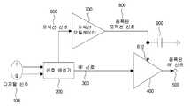
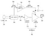
도 1은 포락선 추적 전력 증폭장치를 예시적으로 도시한 도면이다.
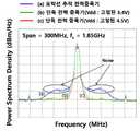
도 2는 종래의 단독 전력 증폭기 및 커패시터를 구비하지 않은 포락선 추적 전력 증폭장치의 출력 스펙트럼을 나타낸 그래프이다.
도 3은 종래의 단독 전력 증폭기, 커패시터를 구비하지 않은 포락선 추적 전력 증폭장치, 및 커패시터를 구비한 포락선 추적 전력 증폭장치의 출력 스펙트럼을 나타낸 그래프이다.
도 4는 포락선 추적 전력증폭장치에서 포락선 모듈레이터의 구성을 예시적으로 도시한 도면이다.
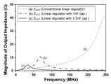
도 5는 병렬로 연결된 커패시터에 의한 포락선 모듈레이터의 출력 임피던스가 낮아지는 결과를 나타낸 그래프이다.
도 6은 포락선 추적 전력증폭장치에서 선형증폭기의 구성을 예시적으로 도시한 도면이다.
도 7은 포락선 추적 전력 증폭장치가 다수 개의 스테이지(stage)를 가진 전력증폭기에 적용될 실시예를 예시적으로 나타낸 도면이다.Hereinafter, the present invention will be described with reference to the embodiments shown in the accompanying drawings. For the sake of clarity, throughout the accompanying drawings, like elements have been assigned the same reference numerals. It is to be understood that the present invention is not limited to the embodiments illustrated in the accompanying drawings, but may be embodied in many other specific forms without departing from the spirit or essential characteristics thereof.
1 is a diagram illustrating an exemplary envelope tracking power amplifying device.
2 is a graph showing an output spectrum of a conventional single power amplifier and an envelope tracking power amplifier without a capacitor.
3 is a graph showing an output spectrum of a conventional single power amplifier, an envelope tracking power amplifier without a capacitor, and an envelope tracking power amplifier with a capacitor.
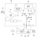
4 is a diagram illustrating an exemplary configuration of an envelope modulator in an envelope tracking power amplifying apparatus.
5 is a graph showing a result of lowering the output impedance of the envelope modulator by the capacitors connected in parallel.
6 is a diagram exemplarily showing a configuration of a linear amplifier in an envelope tracking power amplifying device.
7 is an exemplary diagram illustrating an embodiment in which an envelope tracking power amplifying device is applied to a power amplifier having a plurality of stages.
본 발명은 다양한 변경을 가할 수 있고 여러 가지 실시예를 가질 수 있는 바, 특정 실시예들을 도면에 예시하고 이를 상세한 설명을 통해 상세히 설명하고자 한다. 그러나, 이는 본 발명을 특정한 실시 형태에 대해 한정하려는 것이 아니며, 본 발명의 사상 및 기술 범위에 포함되는 모든 변경, 균등물 내지 대체물을 포함하는 것으로 이해되어야 한다.
While the present invention has been described in connection with certain exemplary embodiments, it is to be understood that the invention is not limited to the disclosed embodiments, but, on the contrary, is intended to cover various modifications and similarities. It should be understood, however, that the invention is not intended to be limited to the particular embodiments, but includes all modifications, equivalents, and alternatives falling within the spirit and scope of the invention.
도 1은 포락선 추적 전력 증폭장치를 예시적으로 도시한 도면이고, 도 2는 종래의 단독 전력 증폭기 및 커패시터를 구비하지 않은 포락선 추적 전력 증폭장치의 출력 스펙트럼을 나타낸 그래프이고, 도 3은 종래의 단독 전력 증폭기, 커패시터를 구비하지 않은 포락선 추적 전력 증폭장치, 및 커패시터를 구비한 포락선 추적 전력 증폭장치의 출력 스펙트럼을 나타낸 그래프이다.2 is a graph showing an output spectrum of a conventional single power amplifier and an envelope tracking power amplifying device without a capacitor, and FIG. 3 is a graph showing an output spectrum of a conventional single power amplifier and a conventional single- A power amplifier, an envelope tracking power amplifier without a capacitor, and an envelope tracking power amplifier with a capacitor.
도 1을 참조하면, 포락선 추적 전력 증폭장치는 입력된 디지털 신호(100)를 RF 신호(300)로 변환하여 출력하는 신호 생성기(200), 신호 생성기(200)로부터 출력된 포락선 입력 신호(600)를 증폭하는 넓은 대역폭을 가지는 포락선 모듈레이터(700), 및 증폭된 포락선 신호(800)에 따라 RF 신호(300)를 증폭하여 증폭된 RF 신호(500)를 출력하는 전력증폭기(400), 및 포락선 모듈레이터의 출력단에 일단이 연결되고 타단은 접지에 연결되어 수신밴드 잡음을 줄이는 커패시터(900)로 구성된다.1, an envelope tracking power amplifying apparatus includes a
포락선 모듈레이터(700)는 선형증폭기(710)와 스위치 증폭기(730)로 구성되며, 넓은 대역폭을 가진다. 포락선 모듈레이터(700)에서, 포락선 입력 신호(600)의 저주파 성분들은 스위치 증폭기(730)에 의해서 증폭이 되고, 고주파 성분들은 선형증폭기(710)에 의해서 증폭된다. 따라서 더 넓은 대역폭을 가지는 포락선 모듈레이터(700)는 더 넓은 대역폭을 가지는, 즉 더 빠른 스피드를 가지는 선형증폭기(710)를 설계함으로써 가능하다. 포락선 모듈레이터(700)는 도 4를 참조하여 설명한다.The
포락선 모듈레이터(700)가 출력한 증폭된 포락선 신호(800)는 전력 증폭기(400)의 전원공급부(Vdd)(810)에 공급된다. 이때 포락선 모듈레이터(100)와 병렬로 연결된 커패시터(900)는 전력 증폭기(400)의 출력 및 수신 밴드의 잡음을 조절할 수 있다. 넓은 대역폭을 가지는 포락선 모듈레이터(100)와 병렬로 연결되어 있는 커패시터(900)는 포락선 추적 전력 증폭장치에서 출력되는 증폭된 RF 신호에 발생하는 스퓨리어스 및 수신 밴드 잡음을 필터링을 통해 제거할 수 있다.The amplified
전력 증폭기(400)의 공급전압을 제어하는 포락선 모듈레이터(100)와 병렬로 연결되어 있는 커패시터(900)의 값은 적절히 선택되어야 한다. 커패시터(900)의 값이 지나치게 작으면, 스퓨리어스 및 수신 밴드 잡음 감소의 효과가 미미해진다. 반대로, 커패시터(900)의 값이 지나치게 크면, 증폭된 포락선 신호(800)가 원하는 크기로 출력되지 않는다. 따라서, 커패시터(900)의 값은 기대하는 잡음 감소 효과와 증폭된 포락선 신호(800)의 크기를 모두 만족할 수 있도록 선택되어야 한다. 예를 들어, 커패시터(900)의 값, 즉, 커패시턴스는 100 pF 이상 수 nF일 수 있다.The value of the
포락선 모듈레이터(700)를 이용하여 전력 증폭기(400)의 전원공급부(Vdd)(810)에 공급전압을 제어하기 위해 도 1과 같이 연결하되, 포락선 모듈레이터(700)에 병렬로 커패시터를 연결하지 않은 포락선 추적 전력 증폭장치와 종래의 단독 전력 증폭기의 출력 스펙트럼을 나타낸 그래프가 도 2에 도시되어 있다.1 for controlling the supply voltage to the power supply unit (Vdd) 810 of the
도 2를 참조하면, 그래프 (a)는 커패시터가 병렬로 연결되지 않은 포락선 추적 전력 증폭장치의 출력 스펙트럼이고, 그래프 (b)는 공급전압 Vdd가 고정된 3.4V인 종래의 단독 전력 증폭기의 출력 스펙트럼이며, 그래프 (c)는 공급전압 Vdd가 고정된 4.5V인 종래의 단독 전력 증폭기의 출력 스펙트럼이 도시되어 있다. 그래프 (b)와 (c)의 경우, 중심 주파수 fc에 전력이 집중되는 반면, 그래프 (a)의 경우 종래의 단독 전력 증폭기에서는 볼 수 없었던 수신 밴드 잡음(receiver band noise)이 발생함을 확인할 수 있다. 휴대용 단말기 및 무선 통신단말기의 전력 증폭기에서 수신 밴드 잡음이 생기게 될 경우 수신을 할 때 원하는 신호와 합쳐지게 되기 때문에 잡음이 발생하게 되어 무선 통신에 있어서 큰 문제가 생기게 된다. 따라서 포락선 추적 전력 증폭장치를 실질적으로 사용하기 위해서는 수신 밴드에 생기는 잡음을 꼭 제거해야 한다.Referring to FIG. 2, graph (a) shows an output spectrum of an envelope tracking power amplifier device in which capacitors are not connected in parallel, and graph (b) shows an output spectrum of a conventional single power amplifier having a fixed supply voltage Vdd of 3.4 V , And graph (c) shows the output spectrum of a conventional single power amplifier with a supply voltage Vdd of 4.5 V fixed. In the graphs (b) and (c), power is concentrated at the center frequency fc, whereas in the case of the graph (a), the receiver band noise which is not seen in the conventional single- have. When a receiving band noise is generated in a power amplifier of a portable terminal and a wireless communication terminal, a noise is generated because a desired signal is received at the time of receiving, which causes a serious problem in wireless communication. Therefore, in order to actually use the envelope tracking power amplifying device, it is necessary to remove the noise generated in the receiving band.
도 3은 커패시터(900)의 추가로 인한 포락선 추적 전력증폭장치의 수신 밴드 잡음이 감소한 최종 실험 결과를 나타낸 그래프이다. 도 3을 참조하면, 그래프 (a)는 단독 전력 증폭기의 출력 스펙트럼이고, 그래프 (b)는 커패시터가 병렬로 연결되지 않은 포락선 추적 전력 증폭장치의 출력 스펙트럼이며, 그래프 (c)는 커패시터가 병렬로 연결된 포락선 추적 전력 증폭장치의 출력 스펙트럼이다. 그래프 (b)를 보면, 포락선 추적 전력 증폭장치의 출력 스펙트럼의 중심 주파수 fc 주위에 스퓨리어스 잡음(spurious noise)이 발생함을 확인할 수 있다. 이에 반해, 그래프 (c)를 보면, 전력 증폭기(200)의 공급전압을 제어하는 포락선 모듈레이터(700)에 병렬로 연결된 커패시터(900)에 의해서 포락선 추적 전력 증폭장치는 출력 스펙트럼에 생기는 수신 밴드 잡음이 크게 줄어들어 저잡음(Low Noise)의 무선통신 단말기 및 시스템의 구현이 가능함을 알 수 있다.
3 is a graph showing a result of a final experiment in which a reception band noise of the envelope tracking power amplifying device due to the addition of the
도 4는 포락선 추적 전력증폭장치에서 포락선 모듈레이터의 구성을 예시적으로 도시한 도면이고, 도 5는 병렬로 연결된 커패시터에 의한 포락선 모듈레이터의 출력 임피던스가 낮아지는 결과를 나타낸 그래프이다.FIG. 4 is a diagram illustrating an exemplary configuration of an envelope modulator in an envelope tracking power amplifying device, and FIG. 5 is a graph illustrating a result of lowering an output impedance of an envelope modulator by a capacitor connected in parallel.
도 4를 참조하면, 포락선 추적 전력증폭장치는 전력증폭기(400)와 포락선 모듈레이터(700)로 구성된다. 전력증폭기(400)는 드라이브 스테이지(410)와 파워 스테이지(420)로 구성될 수 있다. 포락선 모듈레이터(700)는 선형증폭기(710), 선형 전류 감지기(720) 및 스위치 증폭기(730)로 구성될 수 있다. 선형증폭기(710)는 피드백(780)에 의해 포락선 입력 신호(600)를 증폭시키는 독립적인 전압 소스이다. 스위치 증폭기(730)는 출력 전류(770)에 필요한 대부분의 전류를 공급해주는 의존적인 전류 소스이다. 선형 전류 감지기(720)는 선형증폭기(710)에서 출력으로 흐르는 선형 전류(750)의 크기와 방향을 감지하여 스위치 증폭기(730)의 상태를 ON 또는 OFF로 변화시킴으로써 스위치 전류(760)를 조절한다.Referring to FIG. 4, the envelope tracking power amplifying apparatus includes a
포락선 모듈레이터(700)의 전체 효율은 상대적으로 효율이 낮지만 빠른 스피드를 가지는 선형증폭기(710)의 효율과 낮은 스피드를 갖지만 효율이 높은 스위치 증폭기(730)의 효율에 의해 결정된다. 또한, 높은 효율의 포락선 모듈레이터(700)를 설계하기 위해서는 높은 효율의 선형증폭기(710)와 스위치 증폭기(730)를 설계하는 것도 중요하지만 선형증폭기(710)에서 출력되는 선형 전류(750)와 스위치 증폭기(730)에서 출력되는 스위치 전류(760)의 비율도 역시 중요하다. 한편, 포락선 모듈레이터(700)의 동작 가능한 포락선 입력신호(600)의 대역폭은 빠른 스피드를 가지는 선형증폭기(710)에 의해서 정해진다. 다시 말해, 선형증폭기(710)의 대역폭이 넓으면 더 넓은 대역폭을 가지는 포락선 입력신호(600)를 포락선 모듈레이터(700)에 입력할 수 있다는 의미이다. 따라서 포락선 입력신호(600)는 높은 효율의 스위치 증폭기(730)에 의해서 저주파 성분들이 증폭이 되고, 낮은 효율의 선형증폭기(710)에 의해서 고주파 성분들이 증폭된다. 만일 선형증폭기(710)의 대역폭이 좁아서 포락선 입력신호(600)의 고주파 성분을 증폭시킬 수 없다면 포락선 모듈레이터(700)의 출력에 왜곡이 발생하게 된다.The overall efficiency of the
종래의 고정된 공급전압을 사용하는 단독 전력 증폭기는 공급전압을 제공하는 Vdd 선을 통해 들어 오는 잡음을 제거 하기 위해 DC de-coupling 커패시터를 사용한다. 하지만, 포락선 추적 전력 증폭장치는 변조된 포락선이 전력 증폭기의 공급전압으로 사용되기 때문에 DC de-coupling 커패시터를 사용할 수가 없다. 이를 대신하는 것이 포락선 모듈레이터의 선형증폭기(710)이다. 선형증폭기(710)의 출력 임피던스는 아래의 식과 같다.A single power amplifier using a conventional fixed supply voltage uses a DC de-coupling capacitor to remove noise coming through the Vdd line that provides the supply voltage. However, the envelope tracking power amplifier can not use a DC de-coupling capacitor because the modulated envelope is used as the supply voltage of the power amplifier. An alternative to this is the
[수학식 1][Equation 1]

수학식 1에서, Rout은 선형증폭기(710)의 버퍼의 출력 저항이고, β는 피드백(780)의 이득이고, A(s)는 선형증폭기의 주파수 응답이다. 수학식 1에서 알 수 있듯이, 선형증폭기(710)의 출력 임피던스 Zout(s)는 A(s)와 반비례 관계이다. 즉, 선형증폭기(710)의 대역폭이 넓어지면 출력 임피던스 Zout(s)가 낮아지게 된다. 하지만 이것은 한계가 있고, 출력 임피던스 Zout(s)는 주파수가 높아질수록 작아지는 특성을 가지는 것이 아니라 주파수가 높아질수록 출력 임피던스가 커지는 특성을 가지고 있다. 이러한 현상은 A(s)가 주파수가 높아질수록 낮아지기 때문이다.In Equation (1), Rout is the output resistance of the buffer of the
이를 해결하기 위해 도 1과 같이 포락선 모듈레이터(700)에 병렬로 추가적인 커패시터(900)를 연결해주면 포락선 입력신호(600)가 존재하는 0 내지 수십 MHz영역에서는 기존의 포락선 모듈레이터(100)의 특성을 나타내는 그래프 (a)와 유사한 특성을 보이는 반면에, 도 5의 그래프 (b) 및 (c)와 같이 임의의 지점 이후로부터는 추가 커패시터(900) 특성을 갖게 된다. 커패시터의 특성이 나타나는 지점은 커패시터(900)의 크기에 의해 조절될 수 있다. 큰 값을 갖는 커패시터를 병렬로 연결할 경우 수신 밴드에서의 출력 임피던스가 더 낮아져서 잡음이 줄어들 수 있지만, 지나치게 큰 값을 갖는 커패시터를 연결하게 될 경우 포락선 모듈레이터에서 변조된 공급전압을 전력 증폭기에 제대로 전달할 수가 없게 된다. 반대로, 작은 값을 갖는 커패시터를 연결할 경우 잡음 제거 효과가 줄어들게 된다. 따라서 커패시터(900)의 크기는 실험 및/또는 시뮬레이션을 통해 위의 두 가지 경우를 잘 고려하여 적절한 값으로 선택 되어야 한다.
If an
도 6은 포락선 추적 전력증폭장치에서 선형증폭기의 구성을 예시적으로 도시한 도면이다.6 is a diagram exemplarily showing a configuration of a linear amplifier in an envelope tracking power amplifying device.
선형증폭기(710)는 Operational Transconductance Amplifier(OTA)(711), 클래스 AB 바이어스 회로(712), RC 보상 회로(713), 버퍼(714)로 구성된다. OTA(711)는 넓은 대역폭과 높은 DC 이득(gain)을 위해 이득 스테이지로서, 포락선 입력 신호를 수신하며, 출력단은 클래스 AB 바이어스 회로(712)의 입력단에 결합된다. 클래스 AB 바이어스 회로(712)는 PMOS 소스 팔로워와 NMOS 소스 팔로워로 구성되며, 각 게이트가 OTA(711)의 출력단에 결합된다. 버퍼(714)는 큰 전류 전달 능력과 rail-to-rail 동작을 위해 common source 구조로 사용되며, Vdd와 접지 사이에 위치하며, 소스가 서로 연결된 PMOS와 NMOS로 구성된다. 버퍼(714)의 PMOS 및 NMOS의 소스는 출력단으로 동작한다. 버퍼(714)는 높은 효율로 포락선 입력 신호를 왜곡 없이 추적하기 위해서 클래스 AB 바이어스 회로(712)의 소스 팔로워를 이용하여 적절히 바이어스 시킨다. RC 보상 회로(713)는 OTA(711)의 출력단과 버퍼(714)의 출력단 사이에 연결된다.The
RC 보상 회로(713)는 선형증폭기(110)의 Gain Bandwidth Product(GBW)와 Phase Margin(PM)을 결정하는 중요한 요소로서, 선형증폭기(110)가 안정적으로 동작하도록 한다. 큰 커패시터(900)가 포락선 모듈레이터(100)의 출력노드에 추가적으로 연결 되었기 때문에 선형증폭기(110)의 Phase Margin(PM)이 매우 나빠지게 되어 불안전한 동작을 할 수 있다. 따라서, 선형증폭기(110)는 도 6과 같이 RC 보상 회로(713)를 통해서 안정적인 동작을 보장받을 수 있게 된다. 하지만, 일반적으로 대역폭 특성과 Phase Margin(PM) 특성은 trade-off 관계이기 때문에, 추가적인 커패시터를 출력 노드에 연결하고 RC 보상 회로(713)를 통해 안정적인 동작을 보장 받기 위해서는 선형증폭기(110)의 대역폭 특성이 매우 좋아야 한다. 따라서 넓은 대역폭을 가지는 선형증폭기가 필요하다. 대역폭이 넓지 않을 경우, 출력노드에 큰 커패시터가 연결되기 때문에 Phase Margin(PM)을 좋게 하기 위한 RC 보상 회로(713)에 의해 대역폭이 좁아지게 되므로, 고주파를 증폭시키는 선형증폭기(110)가 역할을 제대로 할 수 없게 된다.
The
도 7은 포락선 추적 전력 증폭장치가 다수 개의 스테이지(stage)를 가진 전력증폭기에 적용될 실시예를 예시적으로 나타낸 도면이다.7 is an exemplary diagram illustrating an embodiment in which an envelope tracking power amplifying device is applied to a power amplifier having a plurality of stages.
드라이브 스테이지(410)와 파워 스테이지(420)로 구성된 도 4의 전력증폭기와 비교할 때, 도 7의 전력증폭기는 다수 개의 스테이지로 구성되어 있다. 제안된 포락선 모듈레이터(700) 및 그 출력단에 병렬로 연결되는 커패시터(900)에 의한 잡음 제거 방식은 도 7에서 도시된 바와 같이 단독 혹은 2개의 스테이지를 가진 전력증폭기뿐만 아니라 다수 개의 스테이지를 가진 전력증폭기에도 적용될 수 있다. 도 7과 같이 다수개의 드라이브 스테이지를 가진 전력증폭기의 경우 마지막 스테이지인 파워 스테이지의 전원공급부(Vdd)(810)에 포락선 모듈레이터(100)에서 증폭된 포락선 신호(800)가 공급될 수 있다. 병렬로 연결된 커패시터(900)는 포락선 추적 전력 증폭장치의 출력에 생기는 스퓨리어스 및 수신 밴드 잡음를 필터링을 통해 제거할 수 있다. 다수 개의 스테이지로 구성된 전력 증폭기 역시 상기 언급한 바와 같이 가장 마지막 단의 파워 스테이지의 전원공급부(Vdd)(810)에만 추가 커패시터를 연결하면 스퓨리어스 잡음과 수신 밴드 잡음이 크게 감소될 수 있다.Compared with the power amplifier of FIG. 4, which is comprised of a
커패시터의 크기가 100 pF 내지 수 nF단위의 큰 값이기 때문에 전력증폭기의 드라이브 스테이지와 파워 스테이지에서 가장 마지막 스테이지인 파워 스테이지의 전원공급부(Vdd)(810)에 연결이 되면 스퓨리어스 잡음과 수신 밴드 잡음을 크게 감소시킬 수 있다. 여러 인덕터와 커패시터를 사용하는 구조와 비교하였을 때 파워 스테이지의 추가 커패시터만으로도 불필요한 잡음 성분을 제거하는 구조는 칩 사이즈 측면과 가격적인 측면에서 큰 장점을 가질 수 있다.
Since the magnitude of the capacitor is a large value in the range of 100 pF to several nF, the drive stage of the power amplifier and the power stage (810) of the power stage, which is the last stage in the power stage, Can be greatly reduced. Compared with the structure using several inductors and capacitors, the structure that removes unnecessary noise components by the additional capacitor of the power stage can have a great advantage in terms of chip size and cost.
전술한 본 발명의 설명은 예시를 위한 것이며, 본 발명이 속하는 기술분야의 통상의 지식을 가진 자는 본 발명의 기술적 사상이나 필수적인 특징을 변경하지 않고서 다른 구체적인 형태로 쉽게 변형이 가능하다는 것을 이해할 수 있을 것이다. 그러므로 이상에서 기술한 실시 예들은 모든 면에서 예시적인 것이며 한정적이 아닌 것으로 이해해야만 한다.
It will be understood by those skilled in the art that the foregoing description of the present invention is for illustrative purposes only and that those of ordinary skill in the art can readily understand that various changes and modifications may be made without departing from the spirit or essential characteristics of the present invention. will be. It is therefore to be understood that the above-described embodiments are illustrative in all aspects and not restrictive.
본 발명의 범위는 상기 상세한 설명보다는 후술하는 특허청구범위에 의하여 나타나며, 특허청구범위의 의미 및 범위 그리고 그 균등 개념으로부터 도출되는 모든 변경 또는 변형된 형태가 본 발명의 범위에 포함되는 것으로 해석되어야 한다.
It is intended that the present invention covers the modifications and variations of this invention provided they come within the scope of the appended claims and their equivalents. .
100: 디지털 신호
200: 신호 생성기
300: RF 신호
400: 전력증폭기
500: 증폭된 RF 신호
600: 포락선 입력 신호
700: 포락선 모듈레이터
800: 증폭된 포락선 신호
900: 커패시터100: Digital signal
200: Signal generator
300: RF signal
400: power amplifier
500: amplified RF signal
600: envelope input signal
700: Envelope modulator
800: amplified envelope signal
900: Capacitor
Claims (15)
Translated fromKorean상기 증폭된 포락선 신호에 따라 RF 신호를 증폭하여 증폭된 RF 신호를 출력하는 전력증폭기; 및
상기 포락선 모듈레이터의 출력단에 병렬로 연결된 커패시터를 포함하는 포락선 추적 전력 증폭장치.
An envelope modulator having a wide bandwidth for amplifying an envelope input signal and outputting an amplified envelope signal;
A power amplifier for amplifying an RF signal according to the amplified envelope signal and outputting an amplified RF signal; And
And a capacitor connected in parallel to the output of the envelope modulator.
The apparatus of claim 1, wherein the capacitor filters noise from the envelope modulator and the power amplifier.
3. The envelope tracking power amplifier of claim 2, wherein the capacitor is 100 pF or greater.
3. The apparatus of claim 2, wherein the amplified envelope signal is provided as a supply voltage of the power amplifier.
상기 포락선 모듈레이터는
상기 포락선 입력 신호에 의해 선형 전류를 출력하는 선형증폭기;
상기 선형 전류를 감지하는 선형 전류 감지기; 및
상기 선형 전류 감지기에 의해 스위치 전류를 출력하는 스위치 증폭기를 포함하는 포락선 추적 전력 증폭장치.
3. The method of claim 2,
The envelope modulator
A linear amplifier for outputting a linear current by the envelope input signal;
A linear current sensor for sensing the linear current; And
And a switch amplifier for outputting a switch current by the linear current sensor.
상기 포락선 입력 신호를 입력 받는 OTA(Operational Transconductance Amplifier);
상기 OTA의 출력단에 결합되며 소스 팔로워로 구성된 클래스 AB 바이어스 회로;
상기 클래스 AB 바이어스 회로에 의해 바이어스되며 common source로 구성된 버퍼; 및
상기 OTA의 출력단과 상기 버퍼 사이에 결합되며 상기 선형증폭기의 Phase Margin을 결정하는 RC 보상 회로를 포함하는 포락선 추적 전력 증폭장치.
6. The linear amplifier according to claim 5,
An OTA (Operational Transconductance Amplifier) receiving the envelope input signal;
A class AB bias circuit coupled to an output of the OTA and configured as a source follower;
A buffer biased by the class AB bias circuit and configured as a common source; And
And an RC compensation circuit coupled between the output of the OTA and the buffer to determine a phase margin of the linear amplifier.
3. The apparatus of claim 2, wherein the power amplifier comprises a drive stage and a power stage.
8. The apparatus of claim 7, wherein the drive stage is a plurality of envelope tracking power amplifiers.
8. The apparatus of claim 7, wherein the amplified envelope signal is supplied only to the power stage.
The apparatus of claim 1, further comprising a signal generator for generating the RF signal.
포락선 입력 신호에 의해 선형 전류를 출력하는 넓은 대역폭을 가지는 선형증폭기;
상기 선형 전류를 감지하는 선형 전류 감지기;
상기 선형 전류 감지기에 의해 스위치 전류를 출력하는 스위치 증폭기를 포함하는 포락선 모듈레이터.
An envelope modulator for amplifying an envelope input signal and outputting an amplified envelope signal,
A linear amplifier having a wide bandwidth for outputting a linear current by an envelope input signal;
A linear current sensor for sensing the linear current;
And a switch amplifier for outputting a switch current by the linear current sensor.
상기 포락선 입력 신호를 입력 받는 OTA(Operational Transconductance Amplifier);
상기 OTA의 출력단에 결합되며 소스 팔로워로 구성된 클래스 AB 바이어스 회로;
상기 클래스 AB 바이어스 회로에 의해 바이어스되며 common source로 구성된 버퍼; 및
상기 OTA의 출력단과 상기 버퍼 사이에 결합되며 상기 선형증폭기의 Phase Margin을 결정하는 RC 보상 회로를 포함하는 포락선 모듈레이터.
12. The apparatus of claim 11, wherein the linear amplifier comprises:
An OTA (Operational Transconductance Amplifier) receiving the envelope input signal;
A class AB bias circuit coupled to an output of the OTA and configured as a source follower;
A buffer biased by the class AB bias circuit and configured as a common source; And
And an RC compensation circuit coupled between the output of the OTA and the buffer to determine a phase margin of the linear amplifier.
12. The envelope modulator of claim 11, further comprising a capacitor connected in parallel to an output of the envelope modulator.
상기 커패시터는 상기 전력증폭기의 출력 임피던스 및 주파수 대역폭에 따라 스퓨리어스 잡음 및 수신 밴드 잡음을 조절하는 포락선 모듈레이터.
14. The apparatus of claim 13, wherein the envelope modulator is coupled to a power amplifier,
Wherein the capacitor adjusts spurious noise and receive band noise according to an output impedance and a frequency bandwidth of the power amplifier.
상기 커패시터는 상기 포락선 모듈레이터와 상기 전력증폭기로부터 나오는 잡음을 필터링하는 포락선 모듈레이터.14. The apparatus of claim 13, wherein the envelope modulator is coupled to a power amplifier,
Wherein the capacitor filters noise from the envelope modulator and the power amplifier.
Priority Applications (1)
| Application Number | Priority Date | Filing Date | Title |
|---|---|---|---|
| KR1020150017630AKR20160096288A (en) | 2015-02-04 | 2015-02-04 | Envelope-tracking modulator for reducing spurious noise and receiver band noise and power amplifier with envelope-tracking modulator |
Applications Claiming Priority (1)
| Application Number | Priority Date | Filing Date | Title |
|---|---|---|---|
| KR1020150017630AKR20160096288A (en) | 2015-02-04 | 2015-02-04 | Envelope-tracking modulator for reducing spurious noise and receiver band noise and power amplifier with envelope-tracking modulator |
Publications (1)
| Publication Number | Publication Date |
|---|---|
| KR20160096288Atrue KR20160096288A (en) | 2016-08-16 |
Family
ID=56854303
Family Applications (1)
| Application Number | Title | Priority Date | Filing Date |
|---|---|---|---|
| KR1020150017630AWithdrawnKR20160096288A (en) | 2015-02-04 | 2015-02-04 | Envelope-tracking modulator for reducing spurious noise and receiver band noise and power amplifier with envelope-tracking modulator |
Country Status (1)
| Country | Link |
|---|---|
| KR (1) | KR20160096288A (en) |
Cited By (4)
| Publication number | Priority date | Publication date | Assignee | Title |
|---|---|---|---|---|
| WO2018128420A1 (en)* | 2017-01-06 | 2018-07-12 | Samsung Electronics Co., Ltd. | Power amplification device, terminal having the same, and base station having the same |
| CN109167577A (en)* | 2018-08-30 | 2019-01-08 | 复旦大学 | Low-noise amplifier with envelope detected function |
| CN113949354A (en)* | 2020-07-15 | 2022-01-18 | 联发科技股份有限公司 | Envelope Tracking Power Modulator and Its Wireless Communication System |
| WO2024262754A1 (en)* | 2023-06-22 | 2024-12-26 | 삼성전자주식회사 | Electronic device and method for controlling spurious emission |
Citations (1)
| Publication number | Priority date | Publication date | Assignee | Title |
|---|---|---|---|---|
| US8681898B2 (en) | 2011-04-18 | 2014-03-25 | Electronics And Telecommunications Research Institute | Signal amplifying apparatus, wireless transmitting apparatus, and signal amplifying method |
- 2015
- 2015-02-04KRKR1020150017630Apatent/KR20160096288A/ennot_activeWithdrawn
Patent Citations (1)
| Publication number | Priority date | Publication date | Assignee | Title |
|---|---|---|---|---|
| US8681898B2 (en) | 2011-04-18 | 2014-03-25 | Electronics And Telecommunications Research Institute | Signal amplifying apparatus, wireless transmitting apparatus, and signal amplifying method |
Cited By (7)
| Publication number | Priority date | Publication date | Assignee | Title |
|---|---|---|---|---|
| WO2018128420A1 (en)* | 2017-01-06 | 2018-07-12 | Samsung Electronics Co., Ltd. | Power amplification device, terminal having the same, and base station having the same |
| US10511271B2 (en) | 2017-01-06 | 2019-12-17 | Samsung Electronics Co., Ltd. | Power amplification device, terminal having the same, and base station having the same |
| US11038476B2 (en) | 2017-01-06 | 2021-06-15 | Samsung Electronics Co., Ltd. | Power amplification device, terminal having the same, and base station having the same |
| CN109167577A (en)* | 2018-08-30 | 2019-01-08 | 复旦大学 | Low-noise amplifier with envelope detected function |
| CN109167577B (en)* | 2018-08-30 | 2022-04-12 | 复旦大学 | Low Noise Amplifier with Envelope Detection |
| CN113949354A (en)* | 2020-07-15 | 2022-01-18 | 联发科技股份有限公司 | Envelope Tracking Power Modulator and Its Wireless Communication System |
| WO2024262754A1 (en)* | 2023-06-22 | 2024-12-26 | 삼성전자주식회사 | Electronic device and method for controlling spurious emission |
Similar Documents
| Publication | Publication Date | Title |
|---|---|---|
| US7683720B1 (en) | Folded-cascode amplifier with adjustable continuous time equalizer | |
| JP3541750B2 (en) | Optical receiving preamplifier | |
| US9467106B2 (en) | Wideband bias circuits and methods | |
| EP3574582B1 (en) | Bias modulation active linearization for broadband amplifiers | |
| US20150280672A1 (en) | Low noise amplifier and receiver | |
| CN100481713C (en) | variable gain amplifier | |
| WO2011137635A1 (en) | Power amplifier and method for amplifying signals based on the same | |
| US10122326B2 (en) | Systems and methods providing loadline modulation of a power amplifier | |
| US20050218985A1 (en) | Fully differential amplifier with start up circuit | |
| JP2009165100A5 (en) | ||
| KR20160096288A (en) | Envelope-tracking modulator for reducing spurious noise and receiver band noise and power amplifier with envelope-tracking modulator | |
| KR20190079892A (en) | High frequency signal amplifier including balun | |
| CN105656433A (en) | Low noise amplifier | |
| CN104956589A (en) | Improved RF Low Noise Amplifier Load Circuit | |
| JP4784558B2 (en) | Power amplification device and wireless communication device using the same | |
| US20070096827A1 (en) | Multi controlled output levels cmos power amplifier (pa) | |
| US20110150038A1 (en) | System and method for uwb transmission predistortion and rf wire-bond interface technique related application | |
| US11303248B2 (en) | Dynamically biased power amplification | |
| US8115553B1 (en) | High linearity, low noise, wide bandwidth amplifier/buffer | |
| US8279000B2 (en) | Radio-frequency amplifier | |
| US11437965B2 (en) | Variable gain amplifier and wireless communication device | |
| CN109525211B (en) | Amplifier and wireless signal receiver including said amplifier | |
| CN115940847A (en) | power amplifier | |
| US8310311B2 (en) | Semiconductor integrated circuit device and communication system | |
| US10270411B2 (en) | Amplifier |
Legal Events
| Date | Code | Title | Description |
|---|---|---|---|
| PA0109 | Patent application | Patent event code:PA01091R01D Comment text:Patent Application Patent event date:20150204 | |
| PG1501 | Laying open of application | ||
| PC1203 | Withdrawal of no request for examination | ||
| WITN | Application deemed withdrawn, e.g. because no request for examination was filed or no examination fee was paid |