KR20160094488A - Touch panel and touch display device having the same - Google Patents
Touch panel and touch display device having the sameDownload PDFInfo
- Publication number
- KR20160094488A KR20160094488AKR1020150014906AKR20150014906AKR20160094488AKR 20160094488 AKR20160094488 AKR 20160094488AKR 1020150014906 AKR1020150014906 AKR 1020150014906AKR 20150014906 AKR20150014906 AKR 20150014906AKR 20160094488 AKR20160094488 AKR 20160094488A
- Authority
- KR
- South Korea
- Prior art keywords
- electrode
- substrate
- sensing
- passivation layer
- disposed
- Prior art date
- Legal status (The legal status is an assumption and is not a legal conclusion. Google has not performed a legal analysis and makes no representation as to the accuracy of the status listed.)
- Granted
Links
Images


Classifications
- G—PHYSICS
- G02—OPTICS
- G02F—OPTICAL DEVICES OR ARRANGEMENTS FOR THE CONTROL OF LIGHT BY MODIFICATION OF THE OPTICAL PROPERTIES OF THE MEDIA OF THE ELEMENTS INVOLVED THEREIN; NON-LINEAR OPTICS; FREQUENCY-CHANGING OF LIGHT; OPTICAL LOGIC ELEMENTS; OPTICAL ANALOGUE/DIGITAL CONVERTERS
- G02F1/00—Devices or arrangements for the control of the intensity, colour, phase, polarisation or direction of light arriving from an independent light source, e.g. switching, gating or modulating; Non-linear optics
- G02F1/01—Devices or arrangements for the control of the intensity, colour, phase, polarisation or direction of light arriving from an independent light source, e.g. switching, gating or modulating; Non-linear optics for the control of the intensity, phase, polarisation or colour
- G02F1/13—Devices or arrangements for the control of the intensity, colour, phase, polarisation or direction of light arriving from an independent light source, e.g. switching, gating or modulating; Non-linear optics for the control of the intensity, phase, polarisation or colour based on liquid crystals, e.g. single liquid crystal display cells
- G02F1/133—Constructional arrangements; Operation of liquid crystal cells; Circuit arrangements
- G02F1/1333—Constructional arrangements; Manufacturing methods
- G02F1/13338—Input devices, e.g. touch panels
- G—PHYSICS
- G06—COMPUTING OR CALCULATING; COUNTING
- G06F—ELECTRIC DIGITAL DATA PROCESSING
- G06F3/00—Input arrangements for transferring data to be processed into a form capable of being handled by the computer; Output arrangements for transferring data from processing unit to output unit, e.g. interface arrangements
- G06F3/01—Input arrangements or combined input and output arrangements for interaction between user and computer
- G06F3/03—Arrangements for converting the position or the displacement of a member into a coded form
- G06F3/041—Digitisers, e.g. for touch screens or touch pads, characterised by the transducing means
- G06F3/0416—Control or interface arrangements specially adapted for digitisers
- G—PHYSICS
- G02—OPTICS
- G02F—OPTICAL DEVICES OR ARRANGEMENTS FOR THE CONTROL OF LIGHT BY MODIFICATION OF THE OPTICAL PROPERTIES OF THE MEDIA OF THE ELEMENTS INVOLVED THEREIN; NON-LINEAR OPTICS; FREQUENCY-CHANGING OF LIGHT; OPTICAL LOGIC ELEMENTS; OPTICAL ANALOGUE/DIGITAL CONVERTERS
- G02F1/00—Devices or arrangements for the control of the intensity, colour, phase, polarisation or direction of light arriving from an independent light source, e.g. switching, gating or modulating; Non-linear optics
- G02F1/01—Devices or arrangements for the control of the intensity, colour, phase, polarisation or direction of light arriving from an independent light source, e.g. switching, gating or modulating; Non-linear optics for the control of the intensity, phase, polarisation or colour
- G02F1/13—Devices or arrangements for the control of the intensity, colour, phase, polarisation or direction of light arriving from an independent light source, e.g. switching, gating or modulating; Non-linear optics for the control of the intensity, phase, polarisation or colour based on liquid crystals, e.g. single liquid crystal display cells
- G02F1/133—Constructional arrangements; Operation of liquid crystal cells; Circuit arrangements
- G02F1/1333—Constructional arrangements; Manufacturing methods
- G02F1/1335—Structural association of cells with optical devices, e.g. polarisers or reflectors
- G02F1/133509—Filters, e.g. light shielding masks
- G02F1/133514—Colour filters
- G—PHYSICS
- G02—OPTICS
- G02F—OPTICAL DEVICES OR ARRANGEMENTS FOR THE CONTROL OF LIGHT BY MODIFICATION OF THE OPTICAL PROPERTIES OF THE MEDIA OF THE ELEMENTS INVOLVED THEREIN; NON-LINEAR OPTICS; FREQUENCY-CHANGING OF LIGHT; OPTICAL LOGIC ELEMENTS; OPTICAL ANALOGUE/DIGITAL CONVERTERS
- G02F1/00—Devices or arrangements for the control of the intensity, colour, phase, polarisation or direction of light arriving from an independent light source, e.g. switching, gating or modulating; Non-linear optics
- G02F1/01—Devices or arrangements for the control of the intensity, colour, phase, polarisation or direction of light arriving from an independent light source, e.g. switching, gating or modulating; Non-linear optics for the control of the intensity, phase, polarisation or colour
- G02F1/13—Devices or arrangements for the control of the intensity, colour, phase, polarisation or direction of light arriving from an independent light source, e.g. switching, gating or modulating; Non-linear optics for the control of the intensity, phase, polarisation or colour based on liquid crystals, e.g. single liquid crystal display cells
- G02F1/133—Constructional arrangements; Operation of liquid crystal cells; Circuit arrangements
- G02F1/1333—Constructional arrangements; Manufacturing methods
- G02F1/1343—Electrodes
- G02F1/134309—Electrodes characterised by their geometrical arrangement
- G—PHYSICS
- G06—COMPUTING OR CALCULATING; COUNTING
- G06F—ELECTRIC DIGITAL DATA PROCESSING
- G06F3/00—Input arrangements for transferring data to be processed into a form capable of being handled by the computer; Output arrangements for transferring data from processing unit to output unit, e.g. interface arrangements
- G06F3/01—Input arrangements or combined input and output arrangements for interaction between user and computer
- G06F3/03—Arrangements for converting the position or the displacement of a member into a coded form
- G06F3/041—Digitisers, e.g. for touch screens or touch pads, characterised by the transducing means
- G06F3/0412—Digitisers structurally integrated in a display
Landscapes
- Physics & Mathematics (AREA)
- Engineering & Computer Science (AREA)
- Nonlinear Science (AREA)
- General Physics & Mathematics (AREA)
- General Engineering & Computer Science (AREA)
- Theoretical Computer Science (AREA)
- Crystallography & Structural Chemistry (AREA)
- Chemical & Material Sciences (AREA)
- Optics & Photonics (AREA)
- Mathematical Physics (AREA)
- Human Computer Interaction (AREA)
- Geometry (AREA)
- Liquid Crystal (AREA)
- Devices For Indicating Variable Information By Combining Individual Elements (AREA)
Abstract
Description
Translated fromKorean실시예는 터치 감도를 향상시키기 위한 터치패널 및 이를 포함하는 터치 디스플레이 장치에 관한 것이다.The present invention relates to a touch panel for improving touch sensitivity and a touch display device including the touch panel.
일반적으로, 터치패널은 사용자가 직접 손가락을 이용하거나 물체를 통해서 이미지 디스플레이와 같은 스크린에 디스플레이된 명령 콘텐츠를 선택함으로써 사용자 명령을 입력할 수 있게 해주는 입력 장치이다. 터치 패널이 직접 사용자 손가락에 의해서 또는 물체에 의해서 터치될 때, 터치 패널은 터치 포인트를 검출한 다음 콘텐츠를 디스플레이하기 위해서 선택된 아이콘이 나타내는 커멘드에 따라서 액정 디스플레이를 구동한다.Generally, a touch panel is an input device that allows a user to input user commands by using a finger directly or through an object to select command content displayed on the screen, such as an image display. When the touch panel is directly touched by the user's finger or by an object, the touch panel detects the touch point and then drives the liquid crystal display according to the command indicated by the icon selected to display the content.
터치패널은 일반적으로 액정 디스플레이 내의 터치 패널들의 배치를 기반으로 애드 온 터치패널(Add On Touch Panel)과 인셀 터치패널(In-Cell Touch Panel)로 분류된다.The touch panel is generally classified into an Add On Touch Panel and an In-Cell Touch Panel based on the arrangement of touch panels in a liquid crystal display.
종래 인셀 터치패널은 박막 트랜지스터(Thin Film Transistor; TFT) 기판에 터치 센서 전극을 형성시키고, 컬러필터(Color Filter; CF) 기판의 상부를 터치하여 터치 동작을 구현하고 있다.Conventionally, an insensitive touch panel has a touch sensor electrode formed on a thin film transistor (TFT) substrate and a touch operation is performed by touching an upper portion of a color filter (CF) substrate.
하지만, CF 기판에는 예컨대, 산화인듐주석(Indium Tin Oxide; ITO)재질의 공통 전극이 형성되어 있으며, ITO에 의해 터치 신호가 차단되어 터치 감도가 떨어지는 문제점이 발생된다.However, a common electrode made of, for example, indium tin oxide (ITO) is formed on the CF substrate, and the touch signal is blocked by the ITO, thereby causing a problem that the touch sensitivity is reduced.
상기와 같은 문제점을 해결하기 위해, 실시예는 터치 감도를 향상시키기 위한 터치패널 및 이를 포함하는 터치 디스플레이 장치를 제공하는 것을 그 목적으로 한다.In order to solve the above problems, it is an object of the present invention to provide a touch panel for improving touch sensitivity and a touch display device including the touch panel.
상술한 목적을 달성하기 위하여, 실시예에 따른 터치패널은 CF 기판과, 상기 CF 기판 상에 배치되어 사용자에 의해 터치되며, 상기 터치를 감지하도록 센싱 전극들 및 구동 전극들을 포함하는 TFT 기판과, 상기 CF 기판과 TFT 기판 사이에 배치되는 액정층을 포함할 수 있다.According to an aspect of the present invention, there is provided a touch panel including: a CF substrate; a TFT substrate disposed on the CF substrate and including sensing electrodes and driving electrodes to be touched by a user, And a liquid crystal layer disposed between the CF substrate and the TFT substrate.
또한, 상술한 목적을 달성하기 위하여, 실시예에 따른 터치 디스플레이 장치는 CF 기판과, 상기 CF 기판 상에 배치되어 사용자에 의해 터치되며, 상기 터치를 감지하도록 센싱 전극들 및 구동 전극들을 포함하는 TFT 기판과, 상기 CF 기판과 TFT 기판 사이에 배치되는 액정층을 포함하는 터치패널과, 상기 터치패널의 아래에 배치된 백라이트 유닛을 포함할 수 있다.According to another aspect of the present invention, there is provided a touch display device including a CF substrate, a TFT disposed on the CF substrate and touching the touch panel, the touch panel comprising sensing electrodes and driving electrodes for sensing the touch, A touch panel including a substrate, a liquid crystal layer disposed between the CF substrate and the TFT substrate, and a backlight unit disposed below the touch panel.
실시예는 TFT 기판을 CF 기판 상에 배치함으로써, CF 기판의 ITO에 의해 터치 신호가 차단되는 것을 방지할 수 있는 효과가 있다.The embodiment has the effect of preventing the touch signal from being blocked by the ITO of the CF substrate by disposing the TFT substrate on the CF substrate.
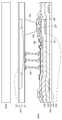
도 1은 실시예에 따른 디스플레이 장치를 나타낸 단면도이다.
도 2는 실시예에 따른 TFT 기판의 어레이를 나타낸 평면도이다.
도 3 내지 도 5는 실시예에 따른 터치패널의 구동 동작을 나타낸 그래프이다.
도 6은 실시예에 따른 터치패널의 터치 패널의 동작을 나타낸 단면도이다.1 is a cross-sectional view illustrating a display device according to an embodiment.
2 is a plan view showing an array of TFT substrates according to an embodiment.
FIGS. 3 to 5 are graphs showing a driving operation of the touch panel according to the embodiment.
6 is a cross-sectional view illustrating the operation of the touch panel of the touch panel according to the embodiment.
이하, 도면을 참조하여 실시예를 상세히 설명하기로 한다.
Hereinafter, embodiments will be described in detail with reference to the drawings.
도 1은 실시예에 따른 디스플레이 장치를 나타낸 단면도이고, 도 2는 실시예에 따른 TFT 기판의 어레이를 나타낸 평면도이고, 도 3 내지 도 5는 실시예에 따른 터치패널의 구동 동작을 나타낸 그래프이고, 도 6은 실시예에 따른 터치패널의 터치 패널의 동작을 나타낸 단면도이다.FIG. 1 is a cross-sectional view illustrating a display device according to an embodiment of the present invention. FIG. 2 is a plan view of an array of TFT substrates according to an embodiment. FIGS. 3 to 5 are graphs illustrating driving operations of a touch panel according to an embodiment, 6 is a cross-sectional view illustrating the operation of the touch panel of the touch panel according to the embodiment.
도 1 및 도 2를 참조하면, 실시예에 따른 터치 디스플레이 장치는 터치패널(1000)과, 상기 터치패널(1000)에 광을 제공하는 백라이트 유닛(2000)을 포함할 수 있다.1 and 2, the touch display apparatus according to the embodiment may include a
터치패널(1000)은 CF 기판(100)과, 상기 CF 기판(100) 상에 배치되어 터치 전극들 및 구동 전극들을 포함하는 TFT 기판(200)과, 상기 CF 기판(100)과 TFT 기판(200) 사이에 배치되는 액정층(300)을 포함할 수 있다. 여기서, CF 기판(100)과 TFT 기판(200) 사이의 가장자리에는 액정층(300)을 가두기 위한 컬럼 스페이서(310)가 배치될 수 있다. 도시되지는 않았으나, CF 기판과, TFT 기판의 일면에는 각각 편광판이 더 배치될 수 있다.The
CF 기판(100)은 제1 유리기판(110)과, 상기 제1 유리기판(100) 상의 컬러 필터(120)와, 상기 컬러 필터(120)를 덮는 오버코트층(130)과, 상기 오버코트층(130) 상에 배치된 제1 공통전극(140)을 포함할 수 있다. 컬러 필터(140)는 적색(Red), 녹색(Green), 파랑(Blue)을 포함할 수 있다. 컬러 필터(140)는 화이트(White)를 더 포함할 수도 있다.The
TFT 기판(200)은 CF 기판(100) 상에 배치될 수 있다. TFT 기판(200)은 구동 전극들(240)과, 센싱 전극들(220)을 포함할 수 있다. 이를 위해 TFT 기판(200)은 매트릭스 형태의 TFT가 형성되어 상기 TFT 들의 소스 전극 및 게이트 전극에는 데이터 라인과 게이트 라인에 각각 연결되고, 드레인 단자에는 화소 전극이 접속된다.The
사용자는 손가락 또는 물체를 이용하여 TFT 기판(200)의 상부에 터치를 수행할 수 있다. 이를 위해 센싱 전극들(220)과 구동 전극들(240)은 서로 교차되도록 배치될 수 있다.The user can perform a touch on the upper portion of the
센싱 전극들(220)은 평면 상 하나의 서브 화소 영역(P)의 가장자리를 따라 배치될 수 있다. 센싱 전극들(220)은 데이터 라인의 방향을 따라 다수의 구간으로 나누어 형성될 수 있으며, 각 구간의 경게면에서는 센싱 전극들(220)이 서로 연결되지 않을 수 있다. 센싱 전극들(220)은 3구간에 걸쳐 나누어 형성될 수 있다.The
센싱 전극들(220)은 각 구간 내에서는 게이트 라인(GL) 방향을 따라 직접 연결될 수 있다. 즉, 인접하는 서브 화소 영역(P)에 배치된 센싱 전극들(220)은 동일층에서 서로 연결되도록 형성할 수 있다.The
센싱 전극들(220)은 데이터 라인(DL) 방향을 따라 인접하는 센싱 전극들(220)과는 브릿지 연결될 수 있다. 센싱 전극들(220)은 데이터 라인(DL)을 따라 배치된 인접하는 센싱 전극들(220)과 일부만 브릿지 연결될 수 있다. 센싱 전극들(220)은 데이터 라인(DL)의 방향을 따라 인접하는 센싱 전극들(220)과 동일층에서 브릿지 연결될 수 있다. 센싱 전극들(220)은 게이트 라인(GL) 방향을 따라 직접 연결되기 때문에 데이터 라인(DL) 방향을 따라 배치된 센싱 전극들(220)은 일부만 브릿지 연결될 수 있다. 센싱 전극들(220)은 백라이트 유닛(2000)의 비개구영역을 차단하여 빛샘 현상을 방지할 수 있는 효과가 있다.The
보다 상세하게 설명하면, TFT 기판(200)은 제2 유리기판(210)과, 상기 제2 유리기판(210)의 아래에 제1 전극(220)이 형성될 수 있다. 제1 전극(220)은 투명한 도전체인 ITO 재질로 형성될 수 있다. 제1 전극(220)은 센싱 전극일 수 있다. 이에 제1 전극(220)은 앞서 설명한 센싱 전극과 동일한 도면 부호를 부여하기로 한다.In more detail, the
제1 전극(220)의 아래에는 제1 페시베이션층(230)이 배치될 수 있다. 제1 페시베이션층(230)은 절연 재질로 형성될 수 있다. 제1 페시베이션층(230)의 아래에는 제2 전극층(240)이 배치될 수 있다. 제2 전극(240)은 게이트 전극일 수 있다. 제2 전극(240)은 구동 전극일 수 있다. 이에 제2 전극(240)은 앞서 설명한 구동 전극과 동일한 도면 부호를 부여하기로 한다.A
제2 전극(240)의 아래에는 제2 전극(240)을 덮도록 절연층(250)이 배치될 수 있다. 절연층(250)의 아래에는 소스 전극(260) 및 드레인 전극(270)이 이격 배치될 수 있다. 소스 전극(260) 및 드레인 전극(270) 상에는 액티브층(ACT)이 소스 전극(260) 및 드레인 전극(270)과 일부가 중첩되도록 배치될 수 있다. 소스 전극(260) 및 드레인 전극(270)의 아래에는 제2 페시베이션층(280)이 배치될 수 있다. 제2 페시베이션층(280)은 소스 전극(260) 및 드레인 전극(270)을 덮도록 배치될 수 있다. 제2 페시베이션층(280)은 절연 재질로 형성될 수 있다. 제2 페시베이션층(280)의 아래에는 화소 전극(290)이 형성될 수 있다. 화소 전극(290)은 제2 페시베이션층(280)에 형성된 홀을 통해 드레인 전극(280)과 전기적으로 연결될 수 있다.An
상기에서는 제1 전극(220)을 센싱 전극으로 사용하고, 제2 전극(240)을 구동 전극으로 사용하였지만, 이에 한정되지 않고 제1 전극(220)을 구동 전극으로 사용하고, 제2 전극(240)을 센싱 전극으로 사용할 수 있다.Although the
도 3에 도시된 바와 같이, 터치 디스플레이 장치는 디스플레이 구간(D)과 센싱 구간(T)을 포함할 수 있다. 디스플레이 구간(D)과 센싱 구간(T)은 1프레임 내에서 시분할되어 구동될 수 있다. 예컨대, 디스플레이 구간(D)과 센싱 구간(T)은 1프레임 내에서 한 번씩 구동될 수 있다.As shown in FIG. 3, the touch display device may include a display period D and a sensing period T. FIG. The display period D and the sensing period T may be time-divisionally driven within one frame. For example, the display period D and the sensing period T may be driven once within one frame.
디스플레이 구간(D)에서는 제1 전극(220)은 공통전극으로 사용되고, 제2 전극(240)은 게이트 전극으로 사용될 수 있다. 센싱 구간(T)에서는 센싱 전극으로 제1 전극(220)이 사용될 수 있으며, 구동 전극으로 제2 전극(240)이 사용될 수 있다. 이와 다르게, 센싱 구간(T)에서는 센싱 전극으로 제2 전극(240)이 사용될 수 있으며, 구동 전극으로 제1 전극(220)이 사용될 수 있다.In the display period D, the
도 4에 도시된 바와 같이, 터치 디스플레이 장치는 디스플레이 구간(D)과 센싱 구간(T)을 포함할 수 있다. 디스플레이 구간(D)과 센싱 구간(T)은 1프레임 내에서 시분할되어 구동될 수 있다. 예컨대, 디스플레이 구간(D)과 센싱 구간(T)은 1프레임 내에서 두 번씩 구동될 수 있다. 디스플레이 구간(D)과 센싱 구간(T)이 한 쌍을 이루어 구동될 수 있으며, 이후 디스플레이 구간(D)과 센싱 구간(T)이 한 쌍을 이루어 다시 구동될 수 있다.As shown in FIG. 4, the touch display device may include a display period D and a sensing period T. FIG. The display period D and the sensing period T may be time-divisionally driven within one frame. For example, the display period D and the sensing period T may be driven twice within one frame. The display period D and the sensing period T may be driven as a pair and then the display period D and the sensing period T may be driven again to form a pair.
디스플레이 구간(D)에서는 제1 전극(220)은 공통전극으로 사용되고, 제2 전극(240)은 게이트 전극으로 사용될 수 있다. 센싱 구간(T)에서는 센싱 전극으로 제1 전극(220)이 사용될 수 있으며, 구동 전극으로 제2 전극(240)이 사용될 수 있다. 이와 다르게, 센싱 구간(T)에서는 센싱 전극으로 제2 전극(240)이 사용될 수 있으며, 구동 전극으로 제1 전극(220)이 사용될 수 있다.In the display period D, the
도 5에 도시된 바와 같이, 터치 디스플레이 장치는 디스플레이 구간(D)과 센싱 구간(T)을 포함할 수 있다. 디스플레이 구간(D)과 센싱 구간(T)은 1프레임 내에서 시분할되어 구동될 수 있다. 예컨대, 디스플레이 구간(D)과 센싱 구간(T)은 1프레임 내에서 두 번이상, 예컨대, N번씩 구동될 수 있다.As shown in FIG. 5, the touch display device may include a display period D and a sensing period T. FIG. The display period D and the sensing period T may be time-divisionally driven within one frame. For example, the display period D and the sensing period T may be driven twice or more, for example, N times within one frame.
디스플레이 구간(D)에서는 제1 전극(220)은 공통전극으로 사용되고, 제2 전극(240)은 게이트 전극으로 사용될 수 있다. 센싱 구간(T)에서는 센싱 전극으로 제1 전극(220)이 사용될 수 있으며, 구동 전극으로 제2 전극(240)이 사용될 수 있다. 이와 다르게, 센싱 구간(T)에서는 센싱 전극으로 제2 전극(240)이 사용될 수 있으며, 구동 전극으로 제1 전극(220)이 사용될 수 있다.In the display period D, the
도 3 내지 도 5에 도시된 바와 같이, 디스플레이 구간(D)과 센싱 구간(T)은 다양한 방식에 의해 시분할되어 구동될 수 있다. 물론, 도 3 내지 도 5에 도시된 특징에 한정되지 않으며, 다양한 방식으로 디스플레이 구간과 센싱 구간을 시분할하여 구동할 수 있다.As shown in FIGS. 3 to 5, the display period D and the sensing period T may be time-divisionally driven by various methods. Of course, the present invention is not limited to the features shown in Figs. 3 to 5, and the display section and the sensing section may be time-divisionally driven in various manners.
도 6에 도시된 바와 같이, 사용자에 의해 TFT 기판(200)의 상부가 눌러지면, TFT 기판(200)의 구동 전극(240)과 센싱 전극(220) 사이에 캐패시턴스가 발생되고, 이를 감지하여 터치 영역을 검출할 수 있게 된다.6, capacitance is generated between the driving
상기와 같이, 실시예에 따른 터치패널은 TFT 기판을 CF 기판 상에 배치함으로써, CF 기판의 ITO에 의해 터치 신호가 차단되는 것을 방지할 수 있는 효과가 있다.As described above, the touch panel according to the embodiment has the effect of preventing the touch signal from being blocked by the ITO of the CF substrate by disposing the TFT substrate on the CF substrate.
도 1로 돌아가서, 백라이트 유닛(2000)은 터치패널(1000) 아래에 배치될 수 있다. 백라이트 유닛(2000)은 터치패널의 하부에 배치되며, 터치패널에 광을 제공하는 역할을 한다. 도시되지는 않았으나, 상기 백라이트 유닛(2000)은 광원과, 상기 광원의 일측에 배치된 도광판과, 상기 도광판의 상부에 배치된 광학 시트들과, 상기 도광판의 하부에 배치된 반사 시트를 포함할 수 있다.Returning to Fig. 1, the
광원은 광을 발생시키는 역할을 하며, LED 소자를 포함할 수 있다. LED 소자는 R(Red), G(Green), B(Blue)의 단색광 발광하는 R,G,B 발광 다이오드 이거나 백색광을 발광하는 발광 다이오드일 수 있으며, 사이드뷰형 소자가 사용될 수 있다. 단색광을 발광하는 LED 소자가 사용되는 경우, R,G,B의 단색광 LED 소자를 교대로 일정한 간격으로 배치하여 이로부터 발광하는 단색광을 백색광으로 혼합한 후 터치패널(1000)로 공급할 수 있다. 이와 달리, 백색광을 발광하는 LED 소자가 사용되는 경우, 복수의 LED 소자를 일정 간격 배치하여 백색광을 터치패널(1000)로 공급할 수 있다. 백색광 LED 소자는 청색을 발광하는 청색 LED 소자와 청색의 단색광을 흡수하여 황색 광을 발광하는 형광체로 구성되어, 청색 LED 소자에서 출력되는 청색 단색광과 형광체에서 발광하는 황색 단색광이 혼합되어 백색광으로 터치패널(1000)에 공급될 수 있다.The light source serves to generate light, and may include an LED element. The LED element may be an R, G, B light emitting diode emitting monochromatic light of red (R), green (G) or blue (B), or a light emitting diode emitting white light, and a side view type device may be used. When an LED element emitting a monochromatic light is used, the monochromatic LED elements of R, G, and B are alternately arranged at regular intervals, monochromatic light emitted therefrom may be mixed into white light, and then supplied to the
도광판(Light Guide Plate, LGP)은 광원으로부터 방출되는 광을 터치패널(1000)로 가이드하는 역할을 한다. 도광판의 일측면으로 입사되는 광은 도광판의 내측에 첨가된 확산제에 의해 굴절 및 반사를 반복하여 타측면까지 진행한 후, 도광판의 상부로 출사하게 된다. 이러한 도광판은 점광원 또는 선광원 형태의 광학 분포를 가지는 광을 면광원 형태의 광학 분포를 가지는 광으로 변경시켜주는 역할을 하게 된다.The light guide plate (LGP) guides the light emitted from the light source to the
광학 시트는 도광판의 상부에 배치되어 도광판에서 출사되는 광의 효율을 향상시켜 터치패널(1000)로 공급하는 기능을 수행한다. 광학 시트는 도광판에서 출사된 광을 확산시키는 확산 시트와, 상기 확산 시트에 의해 확산된 광을 집광하여 터치패널(1000)의 전 영역에 균일한 광을 공급하도록 다수의 프리즘 시트로 이루어질 수 있다.The optical sheet is disposed on the upper side of the light guide plate to improve the efficiency of light emitted from the light guide plate and supply the light to the
확산 시트는 통상적으로 1매가 구비되지만 프리즘 시트는 프리즘이 x, y 축 방향으로 수직하는 교차하는 제1 프리즘 시트 및 제2 프리즘 시트를 구비할 수 있다. 제1 프리즘 시트 및 제2 프리즘 시트는 x,y축 방향에서 광을 굴절시켜 광의 직진성을 향상시킬 수 있다.The diffusion sheet is usually provided with one sheet, but the prism sheet may include a first prism sheet and a second prism sheet which intersect perpendicularly to the x and y axis directions of the prism. The first prism sheet and the second prism sheet can refract light in the x and y axis directions to improve the straightness of light.
반사 시트는 도광판의 하부에 배치되며, 도광판으로부터 하부로 출사되는 광을 터치패널(1000)을 향해 반사시키는 역할을 한다. 이러한 반사 시트는 입사광 전체의 반사량을 조절하여 출광면 전체가 균일한 휘도 분포를 가지도록 할 수 있다. 반사 시트는 반사율이 매우 높은 ESR(Enhanced Specular Reflector, ESR) 필름을 사용할 수 있다. ESR 필름은 98% 반사율과 2%의 투과율을 가지는 은색 또는 백색 필름으로서, 반사 시트로 입사되는 광을 대부분 터치패널(1000)을 향해 반사시키게 된다.
The reflective sheet is disposed at a lower portion of the light guide plate and reflects light emitted downward from the light guide plate toward the
상기에서는 도면 및 실시예를 참조하여 설명하였지만, 해당 기술 분야의 숙련된 당업자는 하기의 특허청구범위에 기재된 본 발명의 기술적 사상으로부터 벗어나지 않는 범위 내에서 본 발명은 다양하게 수정 및 변경시킬 수 있음은 이해할 수 있을 것이다.It will be apparent to those skilled in the art that various modifications and variations can be made in the present invention without departing from the spirit and scope of the invention as defined by the appended claims. You will understand.
100: CF 기판200: TFT 기판
210: 제2 유리기판220: 제1 전극
230: 제1 페시베이션층240: 제2 전극
280: 제2 페시베이션층290: 화소 전극
300: 액정층2000: 백라이트 유닛100: CF substrate 200: TFT substrate
210: second glass substrate 220: first electrode
230: first passivation layer 240: second electrode
280: second passivation layer 290: pixel electrode
300: liquid crystal layer 2000: backlight unit
Claims (11)
Translated fromKorean상기 CF 기판 상에 배치되어 사용자에 의해 터치되며, 상기 터치를 감지하도록 센싱 전극들 및 구동 전극들을 포함하는 TFT 기판; 및
상기 CF 기판과 TFT 기판 사이에 배치되는 액정층;을 포함하는 터치패널.CF substrate;
A TFT substrate disposed on the CF substrate and touching by a user and including sensing electrodes and driving electrodes for sensing the touch; And
And a liquid crystal layer disposed between the CF substrate and the TFT substrate.
상기 TFT 기판은 제1 기판과, 상기 제1 기판의 아래에 이격 배치된 제1 전극과, 상기 제1 전극의 아래에 배치된 제1 페시베이션층과, 상기 제1 페시베이션층의 아래에 배치된 제2 전극과, 상기 제2 전극의 아래에 배치된 절연층과, 상기 절연층의 아래에 배치되어 이격 배치된 소스 및 드레인 전극, 상기 소스 및 드레인 전극과 제2 절연층 사이에 배치된 액티브층과, 상기 소스 및 드레인 전극의 아래에 배치된 제2 페시베이션층과, 상기 제2 페시베이션층 아래에 배치되어 상기 제2 페시베이션층에 형성된 홀을 통해 드레인 전극과 전기적으로 연결된 화소 전극을 포함하는 터치패널.The method according to claim 1,
The TFT substrate includes a first substrate, a first electrode spaced below the first substrate, a first passivation layer disposed under the first electrode, and a second passivation layer disposed under the first passivation layer. An active layer disposed between the source and drain electrodes and the second insulating layer; a second electrode disposed under the first electrode; an insulating layer disposed below the second electrode; and source and drain electrodes disposed below and spaced apart from the insulating layer, A second passivation layer disposed under the source and drain electrodes; and a pixel electrode electrically connected to the drain electrode through holes formed in the second passivation layer and disposed below the second passivation layer, Contains a touch panel.
디스플레이 구간 동안 상기 제1 전극은 공통전극 역할을 수행하고, 제2 전극은 게이트 전극 역할을 수행하는 터치패널.3. The method of claim 2,
Wherein the first electrode serves as a common electrode during a display period and the second electrode serves as a gate electrode.
센싱 구간 동안 상기 제1 전극이 센싱 전극으로 사용되면 제2 전극은 구동전극으로 사용되고, 상기 제1 전극이 구동전극으로 사용되면, 제2 전극은 센싱 전극으로 사용되는 터치패널.The method of claim 3,
Wherein the second electrode is used as a driving electrode when the first electrode is used as a sensing electrode during a sensing period and the second electrode is used as a sensing electrode when the first electrode is used as a driving electrode.
상기 디스플레이 구간과 센싱 구간은 1프레임 내에서 시분할 구동을 수행하는 터치패널.5. The method of claim 4,
Wherein the display section and the sensing section perform time division driving within one frame.
상기 제1 전극들은 게이트 라인 방향을 따라 일정 구간으로 나누어 형성되는 터치패널.6. The method according to any one of claims 1 to 5,
Wherein the first electrodes are divided into a predetermined section along a gate line direction.
상기 제1 전극은 데이터 라인의 방향을 따라 인접하는 제1 전극과 동일층에서 브릿지 연결되는 터치패널.The method according to claim 6,
Wherein the first electrode is bridged at the same layer as the first electrode adjacent to the data line in the direction of the data line.
상기 터치패널의 아래에 배치된 백라이트 유닛;을 포함하는 터치 디스플레이 장치.A TFT substrate disposed on the CF substrate, the TFT substrate including a sensing electrode and a driving electrode that are touched by a user and sense the touch; and a liquid crystal layer disposed between the CF substrate and the TFT substrate. Touch panel; And
And a backlight unit disposed below the touch panel.
상기 TFT 기판은 제1 기판과, 상기 제1 기판의 아래에 이격 배치된 제1 전극과, 상기 제1 전극의 아래에 배치된 제1 페시베이션층과, 상기 제1 페시베이션층의 아래에 배치된 제2 전극과, 상기 제2 전극의 아래에 배치된 절연층과, 상기 절연층의 아래에 배치되어 이격 배치된 소스 및 드레인 전극, 상기 소스 및 드레인 전극과 제2 절연층 사이에 배치된 액티브층과, 상기 소스 및 드레인 전극의 아래에 배치된 제2 페시베이션층과, 상기 제2 페시베이션층 아래에 배치되어 상기 제2 페시베이션층에 형성된 홀을 통해 드레인 전극과 전기적으로 연결된 화소 전극을 포함하는 터치 디스플레이 장치.9. The method of claim 8,
The TFT substrate includes a first substrate, a first electrode spaced below the first substrate, a first passivation layer disposed under the first electrode, and a second passivation layer disposed under the first passivation layer. An active layer disposed between the source and drain electrodes and the second insulating layer; a second electrode disposed under the first electrode; an insulating layer disposed below the second electrode; and source and drain electrodes disposed below and spaced apart from the insulating layer, A second passivation layer disposed below the source and drain electrodes and a pixel electrode electrically connected to the drain electrode through holes formed in the second passivation layer and disposed below the second passivation layer, / RTI >
센싱 구간 동안 상기 제1 전극은 센싱 전극이고 제2 전극은 구동 전극이거나, 상기 제1 전극은 구동 전극이고 제2 전극은 센싱 전극인 터치 디스플레이 장치.10. The method of claim 9,
Wherein the first electrode is a sensing electrode and the second electrode is a driving electrode during a sensing period, the first electrode is a driving electrode, and the second electrode is a sensing electrode.
상기 제1 전극은 데이터 라인의 방향을 따라 인접하는 제1 전극과 동일층에서 브릿지 연결되는 터치 디스플레이 장치.11. The method according to any one of claims 8 to 10,
Wherein the first electrode is bridged at the same layer as the first electrode adjacent to the data line in the direction of the data line.
Priority Applications (1)
| Application Number | Priority Date | Filing Date | Title |
|---|---|---|---|
| KR1020150014906AKR102316349B1 (en) | 2015-01-30 | 2015-01-30 | Touch panel and touch display device having the same |
Applications Claiming Priority (1)
| Application Number | Priority Date | Filing Date | Title |
|---|---|---|---|
| KR1020150014906AKR102316349B1 (en) | 2015-01-30 | 2015-01-30 | Touch panel and touch display device having the same |
Publications (2)
| Publication Number | Publication Date |
|---|---|
| KR20160094488Atrue KR20160094488A (en) | 2016-08-10 |
| KR102316349B1 KR102316349B1 (en) | 2021-10-25 |
Family
ID=56713135
Family Applications (1)
| Application Number | Title | Priority Date | Filing Date |
|---|---|---|---|
| KR1020150014906AActiveKR102316349B1 (en) | 2015-01-30 | 2015-01-30 | Touch panel and touch display device having the same |
Country Status (1)
| Country | Link |
|---|---|
| KR (1) | KR102316349B1 (en) |
Cited By (1)
| Publication number | Priority date | Publication date | Assignee | Title |
|---|---|---|---|---|
| KR20180036367A (en)* | 2016-09-30 | 2018-04-09 | 엘지디스플레이 주식회사 | In-cell touch liquid crystal display device and method for fabricating the same |
Citations (7)
| Publication number | Priority date | Publication date | Assignee | Title |
|---|---|---|---|---|
| KR20040084968A (en)* | 2003-03-27 | 2004-10-07 | 비오이 하이디스 테크놀로지 주식회사 | Liquid crystal display |
| KR20120047540A (en)* | 2010-11-04 | 2012-05-14 | 삼성모바일디스플레이주식회사 | Liquid crystal display integrated touch screen panel |
| KR20130015126A (en)* | 2011-08-02 | 2013-02-13 | 엘지디스플레이 주식회사 | Liquid crystal display device with a built-in touch screen and method for manufacturing the same |
| KR20130074975A (en)* | 2011-12-27 | 2013-07-05 | 하이디스 테크놀로지 주식회사 | Capacitive type liquid crystal display device with an embedded touch sensor |
| KR20140052175A (en)* | 2012-10-22 | 2014-05-07 | 엘지디스플레이 주식회사 | Display device with integrated touch screen and method for driving the same |
| KR20140126287A (en)* | 2013-03-25 | 2014-10-30 | 허페이 비오이 옵토일렉트로닉스 테크놀로지 컴퍼니 리미티드 | Capacitive in-cell touch panel and display device |
| KR20140129542A (en)* | 2013-04-30 | 2014-11-07 | 엘지디스플레이 주식회사 | Touch screen display divice |
- 2015
- 2015-01-30KRKR1020150014906Apatent/KR102316349B1/enactiveActive
Patent Citations (7)
| Publication number | Priority date | Publication date | Assignee | Title |
|---|---|---|---|---|
| KR20040084968A (en)* | 2003-03-27 | 2004-10-07 | 비오이 하이디스 테크놀로지 주식회사 | Liquid crystal display |
| KR20120047540A (en)* | 2010-11-04 | 2012-05-14 | 삼성모바일디스플레이주식회사 | Liquid crystal display integrated touch screen panel |
| KR20130015126A (en)* | 2011-08-02 | 2013-02-13 | 엘지디스플레이 주식회사 | Liquid crystal display device with a built-in touch screen and method for manufacturing the same |
| KR20130074975A (en)* | 2011-12-27 | 2013-07-05 | 하이디스 테크놀로지 주식회사 | Capacitive type liquid crystal display device with an embedded touch sensor |
| KR20140052175A (en)* | 2012-10-22 | 2014-05-07 | 엘지디스플레이 주식회사 | Display device with integrated touch screen and method for driving the same |
| KR20140126287A (en)* | 2013-03-25 | 2014-10-30 | 허페이 비오이 옵토일렉트로닉스 테크놀로지 컴퍼니 리미티드 | Capacitive in-cell touch panel and display device |
| KR20140129542A (en)* | 2013-04-30 | 2014-11-07 | 엘지디스플레이 주식회사 | Touch screen display divice |
Cited By (1)
| Publication number | Priority date | Publication date | Assignee | Title |
|---|---|---|---|---|
| KR20180036367A (en)* | 2016-09-30 | 2018-04-09 | 엘지디스플레이 주식회사 | In-cell touch liquid crystal display device and method for fabricating the same |
Also Published As
| Publication number | Publication date |
|---|---|
| KR102316349B1 (en) | 2021-10-25 |
Similar Documents
| Publication | Publication Date | Title |
|---|---|---|
| TWI758641B (en) | Display device, operating method thereof and integrated control chip | |
| KR101420424B1 (en) | Liquid crystal display device having multi-touch detection function and driving method thereof | |
| US8884900B2 (en) | Touch-sensing display apparatus and electronic device therewith | |
| KR101642146B1 (en) | Touch screen display apparatus | |
| US9830019B2 (en) | Touch-sensing LCD panel | |
| JP4573856B2 (en) | Liquid crystal display device having multi-touch sensing function and driving method thereof | |
| CN101533170B (en) | Liquid crystal display, display system including the liquid crystal display and method of recognizing an object using the liquid crystal display | |
| CN106980850A (en) | A kind of lines detection means and its lines detection method | |
| KR20110032640A (en) | Multi-touch-aware display device | |
| KR20120097761A (en) | Touch integrated display device | |
| US10802653B2 (en) | Touch type display device and method for sensing touch thereof | |
| WO2016188027A1 (en) | Embedded touch display screen and touch display system | |
| US11294217B2 (en) | Transparent display panel and electronic equipment | |
| US8933911B2 (en) | Touch panel integrated display device | |
| KR20120130736A (en) | Liquid crystal display panel and its driving method | |
| CN102662527A (en) | Touch Sensing Display Device | |
| CN110879492A (en) | Liquid crystal display device having a plurality of pixel electrodes | |
| JP2020140085A (en) | In-cell touch panel | |
| KR102316349B1 (en) | Touch panel and touch display device having the same | |
| CN114019739B (en) | Display substrate, display panel and fingerprint identification method | |
| US10216306B2 (en) | Touch panel-equipped display device | |
| KR20160094487A (en) | Touch panel and touch display device having the same | |
| KR101901241B1 (en) | Touch Panel Integrated Display Device | |
| JP2022111590A (en) | Display device | |
| KR102271133B1 (en) | Display device |
Legal Events
| Date | Code | Title | Description |
|---|---|---|---|
| PA0109 | Patent application | St.27 status event code:A-0-1-A10-A12-nap-PA0109 | |
| R17-X000 | Change to representative recorded | St.27 status event code:A-3-3-R10-R17-oth-X000 | |
| R17-X000 | Change to representative recorded | St.27 status event code:A-3-3-R10-R17-oth-X000 | |
| PG1501 | Laying open of application | St.27 status event code:A-1-1-Q10-Q12-nap-PG1501 | |
| P22-X000 | Classification modified | St.27 status event code:A-2-2-P10-P22-nap-X000 | |
| A201 | Request for examination | ||
| PA0201 | Request for examination | St.27 status event code:A-1-2-D10-D11-exm-PA0201 | |
| D13-X000 | Search requested | St.27 status event code:A-1-2-D10-D13-srh-X000 | |
| D14-X000 | Search report completed | St.27 status event code:A-1-2-D10-D14-srh-X000 | |
| E902 | Notification of reason for refusal | ||
| PE0902 | Notice of grounds for rejection | St.27 status event code:A-1-2-D10-D21-exm-PE0902 | |
| P11-X000 | Amendment of application requested | St.27 status event code:A-2-2-P10-P11-nap-X000 | |
| P13-X000 | Application amended | St.27 status event code:A-2-2-P10-P13-nap-X000 | |
| P22-X000 | Classification modified | St.27 status event code:A-2-2-P10-P22-nap-X000 | |
| E701 | Decision to grant or registration of patent right | ||
| PE0701 | Decision of registration | St.27 status event code:A-1-2-D10-D22-exm-PE0701 | |
| GRNT | Written decision to grant | ||
| PR0701 | Registration of establishment | St.27 status event code:A-2-4-F10-F11-exm-PR0701 | |
| PR1002 | Payment of registration fee | St.27 status event code:A-2-2-U10-U11-oth-PR1002 Fee payment year number:1 | |
| PG1601 | Publication of registration | St.27 status event code:A-4-4-Q10-Q13-nap-PG1601 | |
| PR1001 | Payment of annual fee | St.27 status event code:A-4-4-U10-U11-oth-PR1001 Fee payment year number:4 | |
| PR1001 | Payment of annual fee | St.27 status event code:A-4-4-U10-U11-oth-PR1001 Fee payment year number:5 |