KR20160091718A - Multi-layer ceramic capacitor assembly - Google Patents
Multi-layer ceramic capacitor assemblyDownload PDFInfo
- Publication number
- KR20160091718A KR20160091718AKR1020150012188AKR20150012188AKR20160091718AKR 20160091718 AKR20160091718 AKR 20160091718AKR 1020150012188 AKR1020150012188 AKR 1020150012188AKR 20150012188 AKR20150012188 AKR 20150012188AKR 20160091718 AKR20160091718 AKR 20160091718A
- Authority
- KR
- South Korea
- Prior art keywords
- electrode
- ceramic capacitor
- multilayer ceramic
- bonding
- forming substrate
- Prior art date
- Legal status (The legal status is an assumption and is not a legal conclusion. Google has not performed a legal analysis and makes no representation as to the accuracy of the status listed.)
- Granted
Links
Images


Classifications
- H—ELECTRICITY
- H01—ELECTRIC ELEMENTS
- H01G—CAPACITORS; CAPACITORS, RECTIFIERS, DETECTORS, SWITCHING DEVICES, LIGHT-SENSITIVE OR TEMPERATURE-SENSITIVE DEVICES OF THE ELECTROLYTIC TYPE
- H01G4/00—Fixed capacitors; Processes of their manufacture
- H01G4/002—Details
- H01G4/018—Dielectrics
- H01G4/06—Solid dielectrics
- H01G4/08—Inorganic dielectrics
- H01G4/12—Ceramic dielectrics
- H01G4/1209—Ceramic dielectrics characterised by the ceramic dielectric material
- H—ELECTRICITY
- H01—ELECTRIC ELEMENTS
- H01G—CAPACITORS; CAPACITORS, RECTIFIERS, DETECTORS, SWITCHING DEVICES, LIGHT-SENSITIVE OR TEMPERATURE-SENSITIVE DEVICES OF THE ELECTROLYTIC TYPE
- H01G2/00—Details of capacitors not covered by a single one of groups H01G4/00-H01G11/00
- H01G2/02—Mountings
- H01G2/06—Mountings specially adapted for mounting on a printed-circuit support
- H01G2/065—Mountings specially adapted for mounting on a printed-circuit support for surface mounting, e.g. chip capacitors
- H—ELECTRICITY
- H01—ELECTRIC ELEMENTS
- H01G—CAPACITORS; CAPACITORS, RECTIFIERS, DETECTORS, SWITCHING DEVICES, LIGHT-SENSITIVE OR TEMPERATURE-SENSITIVE DEVICES OF THE ELECTROLYTIC TYPE
- H01G4/00—Fixed capacitors; Processes of their manufacture
- H01G4/002—Details
- H01G4/005—Electrodes
- H01G4/008—Selection of materials
- H01G4/0085—Fried electrodes
- H—ELECTRICITY
- H01—ELECTRIC ELEMENTS
- H01G—CAPACITORS; CAPACITORS, RECTIFIERS, DETECTORS, SWITCHING DEVICES, LIGHT-SENSITIVE OR TEMPERATURE-SENSITIVE DEVICES OF THE ELECTROLYTIC TYPE
- H01G4/00—Fixed capacitors; Processes of their manufacture
- H01G4/002—Details
- H01G4/228—Terminals
- H01G4/232—Terminals electrically connecting two or more layers of a stacked or rolled capacitor
- H—ELECTRICITY
- H01—ELECTRIC ELEMENTS
- H01G—CAPACITORS; CAPACITORS, RECTIFIERS, DETECTORS, SWITCHING DEVICES, LIGHT-SENSITIVE OR TEMPERATURE-SENSITIVE DEVICES OF THE ELECTROLYTIC TYPE
- H01G4/00—Fixed capacitors; Processes of their manufacture
- H01G4/30—Stacked capacitors
- H—ELECTRICITY
- H05—ELECTRIC TECHNIQUES NOT OTHERWISE PROVIDED FOR
- H05K—PRINTED CIRCUITS; CASINGS OR CONSTRUCTIONAL DETAILS OF ELECTRIC APPARATUS; MANUFACTURE OF ASSEMBLAGES OF ELECTRICAL COMPONENTS
- H05K1/00—Printed circuits
- H05K1/02—Details
- H05K1/0271—Arrangements for reducing stress or warp in rigid printed circuit boards, e.g. caused by loads, vibrations or differences in thermal expansion
- H—ELECTRICITY
- H05—ELECTRIC TECHNIQUES NOT OTHERWISE PROVIDED FOR
- H05K—PRINTED CIRCUITS; CASINGS OR CONSTRUCTIONAL DETAILS OF ELECTRIC APPARATUS; MANUFACTURE OF ASSEMBLAGES OF ELECTRICAL COMPONENTS
- H05K1/00—Printed circuits
- H05K1/02—Details
- H05K1/11—Printed elements for providing electric connections to or between printed circuits
- H05K1/111—Pads for surface mounting, e.g. lay-out
- H—ELECTRICITY
- H05—ELECTRIC TECHNIQUES NOT OTHERWISE PROVIDED FOR
- H05K—PRINTED CIRCUITS; CASINGS OR CONSTRUCTIONAL DETAILS OF ELECTRIC APPARATUS; MANUFACTURE OF ASSEMBLAGES OF ELECTRICAL COMPONENTS
- H05K1/00—Printed circuits
- H05K1/18—Printed circuits structurally associated with non-printed electric components
- H05K1/181—Printed circuits structurally associated with non-printed electric components associated with surface mounted components
- H—ELECTRICITY
- H05—ELECTRIC TECHNIQUES NOT OTHERWISE PROVIDED FOR
- H05K—PRINTED CIRCUITS; CASINGS OR CONSTRUCTIONAL DETAILS OF ELECTRIC APPARATUS; MANUFACTURE OF ASSEMBLAGES OF ELECTRICAL COMPONENTS
- H05K3/00—Apparatus or processes for manufacturing printed circuits
- H05K3/30—Assembling printed circuits with electric components, e.g. with resistor
- H05K3/32—Assembling printed circuits with electric components, e.g. with resistor electrically connecting electric components or wires to printed circuits
- H05K3/34—Assembling printed circuits with electric components, e.g. with resistor electrically connecting electric components or wires to printed circuits by soldering
- H05K3/341—Surface mounted components
- H05K3/3431—Leadless components
- H05K3/3436—Leadless components having an array of bottom contacts, e.g. pad grid array or ball grid array components
- H—ELECTRICITY
- H05—ELECTRIC TECHNIQUES NOT OTHERWISE PROVIDED FOR
- H05K—PRINTED CIRCUITS; CASINGS OR CONSTRUCTIONAL DETAILS OF ELECTRIC APPARATUS; MANUFACTURE OF ASSEMBLAGES OF ELECTRICAL COMPONENTS
- H05K1/00—Printed circuits
- H05K1/02—Details
- H05K1/14—Structural association of two or more printed circuits
- H05K1/141—One or more single auxiliary printed circuits mounted on a main printed circuit, e.g. modules, adapters
- Y—GENERAL TAGGING OF NEW TECHNOLOGICAL DEVELOPMENTS; GENERAL TAGGING OF CROSS-SECTIONAL TECHNOLOGIES SPANNING OVER SEVERAL SECTIONS OF THE IPC; TECHNICAL SUBJECTS COVERED BY FORMER USPC CROSS-REFERENCE ART COLLECTIONS [XRACs] AND DIGESTS
- Y02—TECHNOLOGIES OR APPLICATIONS FOR MITIGATION OR ADAPTATION AGAINST CLIMATE CHANGE
- Y02P—CLIMATE CHANGE MITIGATION TECHNOLOGIES IN THE PRODUCTION OR PROCESSING OF GOODS
- Y02P70/00—Climate change mitigation technologies in the production process for final industrial or consumer products
- Y02P70/50—Manufacturing or production processes characterised by the final manufactured product
Landscapes
- Engineering & Computer Science (AREA)
- Power Engineering (AREA)
- Microelectronics & Electronic Packaging (AREA)
- Manufacturing & Machinery (AREA)
- Chemical & Material Sciences (AREA)
- Ceramic Engineering (AREA)
- Materials Engineering (AREA)
- Inorganic Chemistry (AREA)
- Fixed Capacitors And Capacitor Manufacturing Machines (AREA)
- Ceramic Capacitors (AREA)
Abstract
Translated fromKoreanDescription
Translated fromKorean본 발명은 적층 세라믹 커패시터 조립체에 관한 것이다.The present invention relates to a multilayer ceramic capacitor assembly.
현재 적층 세라믹 커패시터(MLCC)는 휴대전화 등의 이동체 단말기기에 많이 이용되고 있다. 특히, 적층 세라믹 커패시터는 이동체 단말 중 회로기판의 실장용 랜드에 외부전극을 직접 얹어놓고 실장용 랜드와 외부전극을 솔더 등의 접합제로 접합함으로써 회로기판에 전기적 물리적으로 접속될 수 있다.Currently, multilayer ceramic capacitors (MLCC) are widely used in mobile terminals such as mobile phones. Particularly, the multilayer ceramic capacitor can be electrically and physically connected to the circuit board by directly placing the external electrode on the mounting land of the circuit board of the mobile terminal and bonding the mounting land and the external electrode with a bonding agent such as solder.
그러나, 적층 세라믹 커패시터는 인가되는 전압의 변화에 따라서 기계적인 변형이 생길 수 있다. 그리고, 이와 같은 변형이 발생하면, 변형은 회로기판에 전달되어서 회로기판이 진동할 수 있다. 그 결과, 회로기판의 진동 시 사람의 귀에 들리는 진동음(acoustic noise)이 발생할 수 있다.However, the multilayer ceramic capacitor may undergo mechanical deformation due to changes in applied voltage. Then, when such deformation occurs, the deformation is transmitted to the circuit board so that the circuit board can vibrate. As a result, acoustic noise heard by the human ear when the circuit board vibrates can occur.
본 발명의 실시예는 일면에 적층 세라믹 커패시터가 결합되는 전극형성 기판에서 적층 세라믹 커패시터의 외부전극이 형성된 부분과 대응되는 부분에 관통홀을 형성한 적층 세라믹 커패시터 조립체에 관한 것이다.An embodiment of the present invention relates to a multilayer ceramic capacitor assembly in which a through hole is formed in a portion corresponding to a portion where an external electrode of a multilayer ceramic capacitor is formed in an electrode-forming substrate where a multilayer ceramic capacitor is coupled on one surface.
여기서, 적층 세라믹 커패시터 조립체는 회로기판이 전극형성 기판의 타면에 결합되면서도 관통홀을 통해 회로기판의 일면에 형성된 표면전극이 적층 세라믹 커패시터의 외부전극에 전기적으로 연결될 수 있다.Here, the multilayer ceramic capacitor assembly may be such that the circuit board is coupled to the other surface of the electrode-formed substrate, and the surface electrode formed on one surface of the circuit board through the through hole is electrically connected to the external electrode of the multilayer ceramic capacitor.
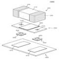
도 1은 본 발명의 일 실시예에 따른 적층 세라믹 커패시터 조립체를 나타내는 사시도.
도 2는 본 발명의 일 실시예에 따른 적층 세라믹 커패시터 조립체를 나타내는 분해 사시도.
도 3은 본 발명의 일 실시예에 따른 적층 세라믹 커패시터 조립체를 나타내는 단면도.
도 4는 본 발명의 일 실시예에 따른 적층 세라믹 커패시터 조립체에서 적층 세라믹 커패시터를 보다 상세히 나타내는 단면도.1 is a perspective view illustrating a multilayer ceramic capacitor assembly in accordance with an embodiment of the present invention;
2 is an exploded perspective view illustrating a multilayer ceramic capacitor assembly in accordance with one embodiment of the present invention.
3 is a cross-sectional view illustrating a multilayer ceramic capacitor assembly in accordance with an embodiment of the present invention.
4 is a cross-sectional view illustrating multilayer ceramic capacitors in more detail in a multilayer ceramic capacitor assembly in accordance with an embodiment of the present invention.
본 출원에서 사용한 용어는 단지 특정한 실시예를 설명하기 위해 사용된 것으로, 본 발명을 한정하려는 의도가 아니다. 단수의 표현은 문맥상 명백하게 다르게 뜻하지 않는 한, 복수의 표현을 포함한다.The terminology used in this application is used only to describe a specific embodiment and is not intended to limit the invention. The singular expressions include plural expressions unless the context clearly dictates otherwise.
본 출원에서, 어떤 부분이 어떤 구성요소를 "포함"한다고 할 때, 이는 특별히 반대되는 기재가 없는 한 다른 구성요소를 제외하는 것이 아니라 다른 구성요소를 더 포함할 수 있는 것을 의미한다. 또한, 명세서 전체에서, "상에"라 함은 대상 부분의 위 또는 아래에 위치함을 의미하는 것이며, 반드시 중력 방향을 기준으로 상 측에 위치하는 것을 의미하는 것이 아니다.In the present application, when a component is referred to as "comprising ", it means that it can include other components as well, without excluding other components unless specifically stated otherwise. Also, throughout the specification, the term "on" means to be located above or below the object portion, and does not necessarily mean that the object is located on the upper side with respect to the gravitational direction.
또한, 결합이라 함은, 각 구성 요소 간의 접촉 관계에 있어, 각 구성 요소 간에 물리적으로 직접 접촉되는 경우만을 뜻하는 것이 아니라, 다른 구성이 각 구성 요소 사이에 개재되어, 그 다른 구성에 구성 요소가 각각 접촉되어 있는 경우까지 포괄하는 개념으로 사용하도록 한다.In addition, the term " coupled " is used not only in the case of direct physical contact between the respective constituent elements in the contact relation between the constituent elements, but also means that other constituent elements are interposed between the constituent elements, Use them as a concept to cover each contact.
또한, 이하 사용되는 제1, 제2 등과 같은 용어는 동일 또는 상응하는 구성 요소들을 구별하기 위한 식별 기호에 불과하며, 동일 또는 상응하는 구성 요소들이 제1, 제2 등의 용어에 의하여 한정되는 것은 아니다.It is also to be understood that the terms first, second, etc. used hereinafter are merely reference numerals for distinguishing between identical or corresponding components, and the same or corresponding components are defined by terms such as first, second, no.
도면에서 나타난 각 구성의 크기 및 두께는 설명의 편의를 위해 임의로 나타내었으므로, 본 발명이 반드시 도시된 바에 한정되지 않는다.The sizes and thicknesses of the respective components shown in the drawings are arbitrarily shown for convenience of explanation, and thus the present invention is not necessarily limited to those shown in the drawings.
이하, 본 발명에 따른 적층 세라믹 커패시터 조립체의 실시예를 첨부도면을 참조하여 상세히 설명하기로 하며, 첨부 도면을 참조하여 설명함에 있어, 동일하거나 대응하는 구성 요소는 동일한 도면번호를 부여하고 이에 대한 중복되는 설명은 생략하기로 한다.DETAILED DESCRIPTION OF THE PREFERRED EMBODIMENTS Hereinafter, embodiments of a multilayer ceramic capacitor assembly according to the present invention will be described in detail with reference to the accompanying drawings, wherein like reference numerals refer to like or corresponding components, The description will be omitted.
도 1은 본 발명의 일 실시예에 따른 적층 세라믹 커패시터 조립체를 나타내는 사시도이다. 도 2는 본 발명의 일 실시예에 따른 적층 세라믹 커패시터 조립체를 나타내는 분해 사시도이다. 도 3은 본 발명의 일 실시예에 따른 적층 세라믹 커패시터 조립체를 나타내는 단면도이다. 도 4는 본 발명의 일 실시예에 따른 적층 세라믹 커패시터 조립체에서 적층 세라믹 커패시터를 보다 상세히 나타내는 단면도이다.1 is a perspective view illustrating a multilayer ceramic capacitor assembly according to one embodiment of the present invention. 2 is an exploded perspective view illustrating a multilayer ceramic capacitor assembly according to one embodiment of the present invention. 3 is a cross-sectional view illustrating a multilayer ceramic capacitor assembly in accordance with an embodiment of the present invention. 4 is a cross-sectional view illustrating multilayer ceramic capacitors in more detail in a multilayer ceramic capacitor assembly in accordance with an embodiment of the present invention.
도 1 내지 도 4에 도시된 바와 같이, 본 발명의 일 실시예에 따른 적층 세라믹 커패시터 조립체(1000)는 적층 세라믹 커패시터(100) 및 전극형성 기판(200)을 포함하고, 제1 접합부(300), 회로기판(400) 및 제2 접합부(500)를 더 포함할 수 있다.1 to 4, a multilayer
적층 세라믹 커패시터(100)는 유전체층(111)과 내부전극(113)을 순차적으로 적층한 적층체(110)와, 내부전극(113)과 전기적으로 연결되어 적층체(110)의 단부에 형성된 외부전극(120)을 포함한다.The multilayer
즉, 도 4에 도시된 바와 같이, 적층 세라믹 커패시터(100)의 적층체(110)는 세라믹 입자를 함유하는 유전체층(111)과 내부전극(113)이 교대로 순차 적층되어 형성된다.That is, as shown in FIG. 4, the
그리고, 외부전극(120)은 적층체(110)의 양단부에 한 쌍으로 형성되고 내부전극(113)이 각각의 외부전극(120)에 전기적으로 연결될 수 있다. 이와 같은 한 쌍의 외부전극(120)은 적층체(110)의 양단부에 형성되어 서로 대향할 수 있으며, 구리 등의 전도성 물질로 이루어질 수 있다.The
전극형성 기판(200)은 일면에 적층 세라믹 커패시터(100)가 결합되고, 외부전극(120)이 형성된 부분과 대응되는 부분에 관통홀(210)이 형성되는 부분으로, 적층 세라믹 커패시터(100)가 후술할 회로기판(400) 등에 실장되는 경우 절연 기능 등을 수행하기 위해 적층 세라믹 커패시터(100)와 회로기판(400) 사이에 개재될 수 있다.The
이 경우, 절연 기능 등을 효과적을 수행하기 위해서는 적층 세라믹 커패시터(100)가 회로기판(400) 등에 실장되는 면 전체를 전극형성 기판(200)이 커버하는 것이 바람직할 수 있으나, 이와 같은 경우에는 적층 세라믹 커패시터(100)와 회로기판(400) 간의 전기적 연결이 곤란해질 수 있다.In this case, in order to effectively perform the insulating function or the like, it is preferable that the
또한, 적층 세라믹 커패시터(100)가 회로기판(400) 등과 대면적이 물리적으로 직접 접합되는 경우에는 적층 세라믹 커패시터(100)에서 발생한 진동이 회로기판(400)으로 그대로 전달되어 진동음(acoustic noise)이 발생할 수 있다.In the case where the multilayer
따라서, 본 실시예에 따른 적층 세라믹 커패시터 조립체(1000)는 적층 세라믹 커패시터(100)의 실장면을 커버하는 전극형성 기판(200)에 관통홀(210)을 형성하고, 이러한 관통홀(210)을 통해 적층 세라믹 커패시터(100)의 전기적 연결이 이루어지도록 할 수 있다.Therefore, the multilayer
이로 인해, 적층 세라믹 커패시터(100)의 실장면 중 상대적으로 최소의 면적만이 노출되므로 절연 성능을 보다 향상시킬 수 있을 뿐만 아니라, 전기적 연결을 보다 용이하게 수행할 수 있다.Accordingly, since only a relatively small area of the mounting surface of the multilayer
제1 접합부(300)는 적층 세라믹 커패시터(100) 및 전극형성 기판(200) 중 외부전극(120)이 형성되지 않은 부분에 형성되어 적층 세라믹 커패시터(100)와 전극형성 기판(200)을 접합시키는 부분으로, 적층 세라믹 커패시터(100)와 전극형성 기판(200)을 물리적으로 접합시킬 수 있다.The
즉, 도 1 내지 도 3에 도시된 바와 같이 적층체(110)의 양단에 외부전극(120)이 형성된 경우, 제1 접합부(300)는 적층체(110)의 중앙 부분에 형성될 수 있다.That is, when the
이 경우, 제1 접합부(300)는 접착 물질 등을 포함하여 적층 세라믹 커패시터(100)와 전극형성 기판(200)을 접착시키거나, 결속 부재 등을 포함하여 적층 세라믹 커패시터(100)와 전극형성 기판(200)을 결속시키는 등 다양하게 구성될 수 있다.In this case, the
이와 같이, 본 실시예에 따른 적층 세라믹 커패시터 조립체(1000)는 제1 접합부(300)를 더 포함하여, 적층 세라믹 커패시터(100)와 전극형성 기판(200) 간의 전기적 연결 경로와 물리적 접합 경로를 서로 분리시킬 수 있다.As described above, the multilayer
여기서, 제1 접합부(300)는 적층 세라믹 커패시터(100) 및 전극형성 기판(200) 각각과 일체로 형성되는 한 쌍의 제1 접합패드(310) 및 한 쌍의 제1 접합패드(310)를 서로 솔더링(soldering) 접합시키는 제1 접합솔더체(320)를 포함할 수 있다.The
즉, 적층 세라믹 커패시터(100)를 회로기판(400) 등에 실장하는 경우에 가장 널리 사용되는 솔더링 접합을 통해 적층 세라믹 커패시터(100) 및 전극형성 기판(200)을 보다 용이하고 효과적으로 접합시킬 수 있다.That is, when the multilayer
회로기판(400)은 일면에 표면전극(410)이 형성되어 관통홀(210)을 통해 표면전극(410)이 외부전극(120)에 전기적으로 연결되도록 전극형성 기판(200)의 타면에 결합되는 부분으로, 소정의 회로 패턴이 형성되어 적층 세라믹 커패시터(100)로 전기적 신호를 제공할 수 있다.The
이 경우, 적층 세라믹 커패시터(100)과 회로기판(400) 간의 전기적 연결은 관통홀(210)을 통해 최소한의 면적만으로 이루어지므로, 적층 세라믹 커패시터(100)의 진동이 회로기판(400)으로 직접 전달되는 것을 최소화할 수 있다.In this case, since the electrical connection between the multilayer
본 실시예에 따른 적층 세라믹 커패시터 조립체(1000)에서 전극형성 기판(200)은 표면전극(410)과 외부전극(120)이 전기적으로 연결되도록 관통홀(210)을 통해 표면전극(410)과 외부전극(120)을 솔더링 접합시키는 통전솔더체(420)를 포함할 수 있다.In the multilayer
즉, 솔더링 접합을 통해 표면전극(410)과 외부전극(120)을 보다 용이하고 효과적으로 전기적 연결시킬 수 있다. 이 경우, 표면전극(410) 상에 일정 부분 유동성이 있는 통전솔더체(420)를 적층한 후, 전극형성 기판(200)을 통전솔더체(420) 상에서 내리 누르면 통전솔더체(420)가 관통홀(210)을 따라 올라오며 외부전극(120)과도 접촉될 수 있다.That is, the
제2 접합부(500)는 전극형성 기판(200) 및 회로기판(400) 중 표면전극(410)이 형성된 부분에 형성되어 전극형성 기판(200)과 회로기판(400)을 접합시키는 부분으로, 전극형성 기판(200)과 회로기판(400)을 물리적으로 접합시킬 수 있다.The
이 경우, 제2 접합부(500) 역시 접착 물질 등을 포함하여 전극형성 기판(200)과 회로기판(400)을 접착시키거나, 결속 부재 등을 포함하여 전극형성 기판(200)과 회로기판(400)을 결속시키는 등 다양하게 구성될 수 있다.In this case, the second
이와 같이, 제2 접합부(500)를 통해 전극형성 기판(200)과 회로기판(400)이 표면전극(410)이 형성된 부분에서 물리적으로 접합된다면, 적층 세라믹 커패시터(100)와 전극형성 기판(200) 간의 물리적 접합은 전극형성 기판(200)의 중앙 부분에서 이루어지고, 전극형성 기판(200)과 회로기판(400) 간의 물리적 접합은 전극형성 기판(200)의 외곽 부분에서 이루어진다.If the
따라서, 적층 세라믹 커패시터(100)의 진동이 전극형성 기판(200)으로 전달되더라도, 다시 전극형성 기판(200)의 외곽 부분으로 진동이 전달된 후 회로기판(400)으로 전달될 수 밖에 없다는 점에서, 상대적으로 비효율적인 진동 전달 경로를 가지게 하여 적층 세라믹 커패시터(100)의 진동이 회로기판(400)으로 전달되는 것을 최소화할 수 있다.Therefore, even if the vibration of the multilayer
여기서, 제2 접합부(500)는 전극형성 기판(200)과 일체로 형성되는 제2 접합패드(510) 및 제2 접합패드(510)와 표면전극(410)을 서로 솔더링 접합시키는 제2 접합솔더체(520)를 포함할 수 있다.The
즉, 솔더링 접합을 통해 전극형성 기판(200)과 회로기판(400)을 보다 용이하고 효과적으로 접합시킬 수 있다. 특히, 제1 접합부(300)를 통한 적층 세라믹 커패시터(100)와 전극형성 기판(200)간의 솔더링 접합과 병행하여 진행할 수 있으므로, 관련 공정을 보다 용이하게 수행할 수 있다.That is, the electrode-forming
나아가, 본 실시예에 따른 적층 세라믹 커패시터 조립체(1000)에서, 통전솔더체(420)와 제2 접합솔더체(520)는 일체로 형성될 수 있다. 즉, 통전솔더체(420)와 제2 접합솔더체(520)를 별도로 형성하지 않고, 표면전극(410) 상에 일정 부분 유동성이 있는 통전솔더체(420)를 적층한 후, 전극형성 기판(200)을 통전솔더체(420) 상에서 내리 눌렀을 때, 관통홀(210)을 따라 올라오는 부분은 자연스럽게 통전솔더체(420)가 되고, 관통홀(210)을 벗어나 전극형성 기판(200)과 회로기판(400) 사이에 개재되는 부분은 자연스럽게 제2 접합솔더체(520)가 될 수 있다.Further, in the multilayer
이와 같이, 통전솔더체(420)와 제2 접합솔더체(520)는 일체로 형성할 수 있으므로, 전기적 연결 및 물리적 접합을 위한 공정을 동시에 수행할 수 있다.Since the energizing
이상, 본 발명의 일 실시예에 대하여 설명하였으나, 해당 기술 분야에서 통상의 지식을 가진 자라면 특허청구범위에 기재된 본 발명의 사상으로부터 벗어나지 않는 범위 내에서, 구성 요소의 부가, 변경, 삭제 또는 추가 등에 의해 본 발명을 다양하게 수정 및 변경시킬 수 있을 것이며, 이 또한 본 발명의 권리범위 내에 포함된다고 할 것이다.It will be apparent to those skilled in the art that various modifications and variations can be made in the present invention without departing from the spirit of the invention as set forth in the appended claims. The present invention can be variously modified and changed by those skilled in the art, and it is also within the scope of the present invention.
100: 적층 세라믹 커패시터
110: 적층체
111: 유전체층
113: 내부전극
120: 외부전극
200: 전극형성 기판
210: 관통홀
300: 제1 접합부
310: 제1 접합패드
320: 제1 접합솔더체
400: 회로기판
410: 표면전극
420: 통전솔더체
500: 제2 접합부
510: 제2 접합패드
520: 제2 접합솔더체
1000: 적층 세라믹 커패시터 조립체100: Multilayer Ceramic Capacitor
110:
111: dielectric layer
113: internal electrode
120: external electrode
200: electrode forming substrate
210: Through hole
300: first connection
310: first bonding pad
320: first bonding solder
400: circuit board
410: surface electrode
420: Energizing solder body
500: second joint
510: second bonding pad
520: second bonding solder body
1000: Multilayer Ceramic Capacitor Assembly
Claims (8)
Translated fromKorean일면에 상기 적층 세라믹 커패시터가 결합되고, 상기 외부전극이 형성된 부분과 대응되는 부분에 관통홀이 형성되는 전극형성 기판;
를 포함하는 적층 세라믹 커패시터 조립체.
A multilayer ceramic capacitor comprising: a multilayer body in which a dielectric layer and an internal electrode are sequentially laminated; and an external electrode electrically connected to the internal electrode and formed at an end of the multilayer body; And
An electrode formation substrate in which the multilayer ceramic capacitor is coupled to one surface and a through hole is formed in a portion corresponding to a portion where the external electrode is formed;
≪ / RTI >
상기 적층 세라믹 커패시터 및 상기 전극형성 기판 중 상기 외부전극이 형성되지 않은 부분에 형성되어 상기 적층 세라믹 커패시터와 상기 전극형성 기판을 접합시키는 제1 접합부;
를 더 포함하는 적층 세라믹 커패시터 조립체.
The method according to claim 1,
A first junction formed at a portion of the multilayer ceramic capacitor and the electrode formation substrate where the external electrode is not formed, and joining the multilayer ceramic capacitor and the electrode formation substrate;
≪ / RTI >
상기 제1 접합부는
상기 적층 세라믹 커패시터 및 상기 전극형성 기판 각각과 일체로 형성되는 한 쌍의 제1 접합패드 및
한 쌍의 상기 제1 접합패드를 서로 솔더링(soldering) 접합시키는 제1 접합솔더체를 포함하는, 적층 세라믹 커패시터 조립체.
3. The method of claim 2,
The first joint
A pair of first bonding pads formed integrally with each of the laminated ceramic capacitor and the electrode forming substrate,
And a first bonding solder body for soldering and bonding a pair of the first bonding pads to each other.
일면에 표면전극이 형성되어 상기 관통홀을 통해 상기 표면전극이 상기 외부전극에 전기적으로 연결되도록 상기 전극형성 기판의 타면에 결합되는 회로기판;
을 더 포함하는 적층 세라믹 커패시터 조립체.
4. The method according to any one of claims 1 to 3,
A circuit board having a surface electrode formed on one surface thereof and coupled to the other surface of the electrode forming substrate so that the surface electrode is electrically connected to the external electrode through the through hole;
≪ / RTI >
상기 전극형성 기판은
상기 표면전극과 상기 외부전극이 전기적으로 연결되도록 상기 관통홀을 통해 상기 표면전극과 상기 외부전극을 솔더링 접합시키는 통전솔더체를 포함하는, 적층 세라믹 커패시터 조립체.
5. The method of claim 4,
The electrode-
And an energizing solder body for soldering the surface electrode and the external electrode through the through hole so that the surface electrode and the external electrode are electrically connected to each other.
상기 전극형성 기판 및 상기 회로기판 중 상기 표면전극이 형성된 부분에 형성되어 상기 전극형성 기판과 상기 회로기판을 접합시키는 제2 접합부;
를 더 포함하는 적층 세라믹 커패시터 조립체.
6. The method of claim 5,
A second bonding portion formed on a portion of the electrode-forming substrate and the circuit substrate where the surface electrode is formed to bond the electrode-forming substrate and the circuit substrate;
≪ / RTI >
상기 제2 접합부는
상기 전극형성 기판과 일체로 형성되는 제2 접합패드 및
상기 제2 접합패드와 상기 표면전극을 서로 솔더링 접합시키는 제2 접합솔더체를 포함하는, 적층 세라믹 커패시터 조립체.
The method according to claim 6,
The second joint
A second bonding pad formed integrally with the electrode forming substrate,
And a second bonding solder body for soldering bonding the second bonding pad and the surface electrode to each other.
상기 통전솔더체와 상기 제2 접합솔더체는 일체로 형성되는, 적층 세라믹 커패시터 조립체.
8. The method of claim 7,
Wherein the conductive solder body and the second bonded solder body are integrally formed.
Priority Applications (3)
| Application Number | Priority Date | Filing Date | Title |
|---|---|---|---|
| KR1020150012188AKR102163037B1 (en) | 2015-01-26 | 2015-01-26 | Multi-layer ceramic capacitor assembly |
| US14/990,332US20160217929A1 (en) | 2015-01-26 | 2016-01-07 | Multi-layer ceramic capacitor assembly |
| US15/851,110US10319525B2 (en) | 2015-01-26 | 2017-12-21 | Multi-layer ceramic capacitor assembly |
Applications Claiming Priority (1)
| Application Number | Priority Date | Filing Date | Title |
|---|---|---|---|
| KR1020150012188AKR102163037B1 (en) | 2015-01-26 | 2015-01-26 | Multi-layer ceramic capacitor assembly |
Publications (2)
| Publication Number | Publication Date |
|---|---|
| KR20160091718Atrue KR20160091718A (en) | 2016-08-03 |
| KR102163037B1 KR102163037B1 (en) | 2020-10-08 |
Family
ID=56434122
Family Applications (1)
| Application Number | Title | Priority Date | Filing Date |
|---|---|---|---|
| KR1020150012188AActiveKR102163037B1 (en) | 2015-01-26 | 2015-01-26 | Multi-layer ceramic capacitor assembly |
Country Status (2)
| Country | Link |
|---|---|
| US (2) | US20160217929A1 (en) |
| KR (1) | KR102163037B1 (en) |
Cited By (1)
| Publication number | Priority date | Publication date | Assignee | Title |
|---|---|---|---|---|
| KR20210123054A (en)* | 2020-04-02 | 2021-10-13 | (주)파트론 | Dielectric filter module |
Families Citing this family (1)
| Publication number | Priority date | Publication date | Assignee | Title |
|---|---|---|---|---|
| WO2022150342A1 (en)* | 2021-01-06 | 2022-07-14 | Bourns, Inc. | Multi-layer electrical device |
Citations (6)
| Publication number | Priority date | Publication date | Assignee | Title |
|---|---|---|---|---|
| US4760948A (en)* | 1986-12-23 | 1988-08-02 | Rca Corporation | Leadless chip carrier assembly and method |
| JPH08222831A (en)* | 1995-02-09 | 1996-08-30 | Matsushita Electric Ind Co Ltd | Mounting body for surface mount components |
| US5931371A (en)* | 1997-01-16 | 1999-08-03 | Ford Motor Company | Standoff controlled interconnection |
| US6693243B1 (en)* | 1999-11-25 | 2004-02-17 | Murata Manufacturing Co, Ltd. | Surface mounting component and mounted structure of surface mounting component |
| KR20090097411A (en) | 2008-03-11 | 2009-09-16 | 엘지이노텍 주식회사 | Noise suppression device and power supply system including the same |
| WO2014126084A1 (en)* | 2013-02-18 | 2014-08-21 | 太陽誘電株式会社 | Multilayer ceramic capacitor with interposer, and interposer for multilayer ceramic capacitor |
Family Cites Families (3)
| Publication number | Priority date | Publication date | Assignee | Title |
|---|---|---|---|---|
| JPH08130364A (en)* | 1994-10-31 | 1996-05-21 | Matsushita Electric Ind Co Ltd | Chip-type electronic component mounting body |
| US20070007323A1 (en)* | 2005-07-06 | 2007-01-11 | International Business Machines Corporation | Standoff structures for surface mount components |
| JP5459445B2 (en)* | 2011-07-11 | 2014-04-02 | 株式会社村田製作所 | Electronic components |
- 2015
- 2015-01-26KRKR1020150012188Apatent/KR102163037B1/enactiveActive
- 2016
- 2016-01-07USUS14/990,332patent/US20160217929A1/ennot_activeAbandoned
- 2017
- 2017-12-21USUS15/851,110patent/US10319525B2/enactiveActive
Patent Citations (6)
| Publication number | Priority date | Publication date | Assignee | Title |
|---|---|---|---|---|
| US4760948A (en)* | 1986-12-23 | 1988-08-02 | Rca Corporation | Leadless chip carrier assembly and method |
| JPH08222831A (en)* | 1995-02-09 | 1996-08-30 | Matsushita Electric Ind Co Ltd | Mounting body for surface mount components |
| US5931371A (en)* | 1997-01-16 | 1999-08-03 | Ford Motor Company | Standoff controlled interconnection |
| US6693243B1 (en)* | 1999-11-25 | 2004-02-17 | Murata Manufacturing Co, Ltd. | Surface mounting component and mounted structure of surface mounting component |
| KR20090097411A (en) | 2008-03-11 | 2009-09-16 | 엘지이노텍 주식회사 | Noise suppression device and power supply system including the same |
| WO2014126084A1 (en)* | 2013-02-18 | 2014-08-21 | 太陽誘電株式会社 | Multilayer ceramic capacitor with interposer, and interposer for multilayer ceramic capacitor |
Cited By (1)
| Publication number | Priority date | Publication date | Assignee | Title |
|---|---|---|---|---|
| KR20210123054A (en)* | 2020-04-02 | 2021-10-13 | (주)파트론 | Dielectric filter module |
Also Published As
| Publication number | Publication date |
|---|---|
| KR102163037B1 (en) | 2020-10-08 |
| US20180114646A1 (en) | 2018-04-26 |
| US20160217929A1 (en) | 2016-07-28 |
| US10319525B2 (en) | 2019-06-11 |
Similar Documents
| Publication | Publication Date | Title |
|---|---|---|
| KR101562597B1 (en) | Electronic component | |
| TWI550662B (en) | Installation of electronic components | |
| KR102426211B1 (en) | Electronic component and board having the same mounted thereon | |
| CN102956353B (en) | Chip-component structure and manufacture method thereof | |
| US9095073B2 (en) | Mounting land structure and mounting structure for laminated capacitor | |
| US9560764B2 (en) | Chip-component structure | |
| US10658118B2 (en) | Electronic component and board having the same | |
| JP5459444B2 (en) | Electronic components | |
| US9620288B2 (en) | Chip-component structure | |
| KR102463337B1 (en) | Electronic component and board having the same mounted thereon | |
| JP5532087B2 (en) | Mounting structure | |
| JP5459368B2 (en) | Chip component structure | |
| KR20160091718A (en) | Multi-layer ceramic capacitor assembly | |
| KR20190098016A (en) | Electronic component and board having the same mounted thereon | |
| JP2008034678A (en) | Sheet substrate base material and electronic device | |
| KR100847647B1 (en) | Printed circuit board | |
| KR20210085668A (en) | Electronic component and board having the same mounted thereon | |
| JP2018060908A (en) | Semiconductor device | |
| RU2016148440A (en) | SENSOR WITH MICROELECTRONIC PRIMARY MEASURING CONVERTER OF INERTIAL TYPE |
Legal Events
| Date | Code | Title | Description |
|---|---|---|---|
| PA0109 | Patent application | St.27 status event code:A-0-1-A10-A12-nap-PA0109 | |
| R17-X000 | Change to representative recorded | St.27 status event code:A-3-3-R10-R17-oth-X000 | |
| PG1501 | Laying open of application | St.27 status event code:A-1-1-Q10-Q12-nap-PG1501 | |
| A201 | Request for examination | ||
| PA0201 | Request for examination | St.27 status event code:A-1-2-D10-D11-exm-PA0201 | |
| P22-X000 | Classification modified | St.27 status event code:A-2-2-P10-P22-nap-X000 | |
| D13-X000 | Search requested | St.27 status event code:A-1-2-D10-D13-srh-X000 | |
| D14-X000 | Search report completed | St.27 status event code:A-1-2-D10-D14-srh-X000 | |
| R18-X000 | Changes to party contact information recorded | St.27 status event code:A-3-3-R10-R18-oth-X000 | |
| E902 | Notification of reason for refusal | ||
| PE0902 | Notice of grounds for rejection | St.27 status event code:A-1-2-D10-D21-exm-PE0902 | |
| P11-X000 | Amendment of application requested | St.27 status event code:A-2-2-P10-P11-nap-X000 | |
| P13-X000 | Application amended | St.27 status event code:A-2-2-P10-P13-nap-X000 | |
| E701 | Decision to grant or registration of patent right | ||
| PE0701 | Decision of registration | St.27 status event code:A-1-2-D10-D22-exm-PE0701 | |
| PR0701 | Registration of establishment | St.27 status event code:A-2-4-F10-F11-exm-PR0701 | |
| PR1002 | Payment of registration fee | St.27 status event code:A-2-2-U10-U11-oth-PR1002 Fee payment year number:1 | |
| PG1601 | Publication of registration | St.27 status event code:A-4-4-Q10-Q13-nap-PG1601 | |
| PR1001 | Payment of annual fee | St.27 status event code:A-4-4-U10-U11-oth-PR1001 Fee payment year number:4 | |
| PR1001 | Payment of annual fee | St.27 status event code:A-4-4-U10-U11-oth-PR1001 Fee payment year number:5 | |
| PR1001 | Payment of annual fee | St.27 status event code:A-4-4-U10-U11-oth-PR1001 Fee payment year number:6 |