KR20160087024A - Thin film transistor and method for fabricaing the same - Google Patents
Thin film transistor and method for fabricaing the sameDownload PDFInfo
- Publication number
- KR20160087024A KR20160087024AKR1020150004151AKR20150004151AKR20160087024AKR 20160087024 AKR20160087024 AKR 20160087024AKR 1020150004151 AKR1020150004151 AKR 1020150004151AKR 20150004151 AKR20150004151 AKR 20150004151AKR 20160087024 AKR20160087024 AKR 20160087024A
- Authority
- KR
- South Korea
- Prior art keywords
- electrode
- oxide semiconductor
- semiconductor pattern
- pattern
- forming
- Prior art date
- Legal status (The legal status is an assumption and is not a legal conclusion. Google has not performed a legal analysis and makes no representation as to the accuracy of the status listed.)
- Withdrawn
Links
- 238000000034methodMethods0.000titleclaimsdescription28
- 239000010409thin filmSubstances0.000titledescription42
- 239000004065semiconductorSubstances0.000claimsabstractdescription132
- 239000000758substrateSubstances0.000claimsabstractdescription52
- 229920002120photoresistant polymerPolymers0.000claimsdescription65
- 239000000463materialSubstances0.000claimsdescription31
- TYHJXGDMRRJCRY-UHFFFAOYSA-Nzinc indium(3+) oxygen(2-) tin(4+)Chemical compound[O-2].[Zn+2].[Sn+4].[In+3]TYHJXGDMRRJCRY-UHFFFAOYSA-N0.000claimsdescription12
- 239000007769metal materialSubstances0.000claimsdescription7
- 238000000151depositionMethods0.000claimsdescription2
- 229910052751metalInorganic materials0.000description14
- 239000002184metalSubstances0.000description14
- 238000004519manufacturing processMethods0.000description13
- 239000010949copperSubstances0.000description11
- 238000005530etchingMethods0.000description9
- 239000010936titaniumSubstances0.000description8
- RYGMFSIKBFXOCR-UHFFFAOYSA-NCopperChemical compound[Cu]RYGMFSIKBFXOCR-UHFFFAOYSA-N0.000description7
- 229910052802copperInorganic materials0.000description7
- 239000010408filmSubstances0.000description7
- 238000004148unit processMethods0.000description7
- ZOKXTWBITQBERF-UHFFFAOYSA-NMolybdenumChemical compound[Mo]ZOKXTWBITQBERF-UHFFFAOYSA-N0.000description6
- 229910052782aluminiumInorganic materials0.000description6
- XAGFODPZIPBFFR-UHFFFAOYSA-NaluminiumChemical compound[Al]XAGFODPZIPBFFR-UHFFFAOYSA-N0.000description6
- 229910052750molybdenumInorganic materials0.000description6
- 239000011733molybdenumSubstances0.000description6
- XLOMVQKBTHCTTD-UHFFFAOYSA-NZinc monoxideChemical compound[Zn]=OXLOMVQKBTHCTTD-UHFFFAOYSA-N0.000description5
- BQCADISMDOOEFD-UHFFFAOYSA-NSilverChemical compound[Ag]BQCADISMDOOEFD-UHFFFAOYSA-N0.000description4
- ATJFFYVFTNAWJD-UHFFFAOYSA-NTinChemical compound[Sn]ATJFFYVFTNAWJD-UHFFFAOYSA-N0.000description4
- RTAQQCXQSZGOHL-UHFFFAOYSA-NTitaniumChemical compound[Ti]RTAQQCXQSZGOHL-UHFFFAOYSA-N0.000description4
- 229910021417amorphous siliconInorganic materials0.000description4
- 239000011651chromiumSubstances0.000description4
- 239000004020conductorSubstances0.000description4
- 229910052733galliumInorganic materials0.000description4
- 229910052709silverInorganic materials0.000description4
- 239000004332silverSubstances0.000description4
- 229910052719titaniumInorganic materials0.000description4
- GYHNNYVSQQEPJS-UHFFFAOYSA-NGalliumChemical compound[Ga]GYHNNYVSQQEPJS-UHFFFAOYSA-N0.000description3
- APFVFJFRJDLVQX-UHFFFAOYSA-Nindium atomChemical compound[In]APFVFJFRJDLVQX-UHFFFAOYSA-N0.000description3
- 238000009413insulationMethods0.000description3
- 229910044991metal oxideInorganic materials0.000description3
- 150000004706metal oxidesChemical class0.000description3
- YVTHLONGBIQYBO-UHFFFAOYSA-Nzinc indium(3+) oxygen(2-)Chemical compound[O--].[Zn++].[In+3]YVTHLONGBIQYBO-UHFFFAOYSA-N0.000description3
- 229910000838Al alloyInorganic materials0.000description2
- VYZAMTAEIAYCRO-UHFFFAOYSA-NChromiumChemical compound[Cr]VYZAMTAEIAYCRO-UHFFFAOYSA-N0.000description2
- XUIMIQQOPSSXEZ-UHFFFAOYSA-NSiliconChemical compound[Si]XUIMIQQOPSSXEZ-UHFFFAOYSA-N0.000description2
- 230000000903blocking effectEffects0.000description2
- 229910052804chromiumInorganic materials0.000description2
- 229910052738indiumInorganic materials0.000description2
- NQBRDZOHGALQCB-UHFFFAOYSA-NoxoindiumChemical compound[O].[In]NQBRDZOHGALQCB-UHFFFAOYSA-N0.000description2
- KYKLWYKWCAYAJY-UHFFFAOYSA-Noxotin;zincChemical compound[Zn].[Sn]=OKYKLWYKWCAYAJY-UHFFFAOYSA-N0.000description2
- 229910052710siliconInorganic materials0.000description2
- 239000010703siliconSubstances0.000description2
- 229910052715tantalumInorganic materials0.000description2
- GUVRBAGPIYLISA-UHFFFAOYSA-Ntantalum atomChemical compound[Ta]GUVRBAGPIYLISA-UHFFFAOYSA-N0.000description2
- JBQYATWDVHIOAR-UHFFFAOYSA-NtellanylidenegermaniumChemical compound[Te]=[Ge]JBQYATWDVHIOAR-UHFFFAOYSA-N0.000description2
- OGIDPMRJRNCKJF-UHFFFAOYSA-Ntitanium(II) oxideChemical compound[Ti]=OOGIDPMRJRNCKJF-UHFFFAOYSA-N0.000description2
- 229910001316Ag alloyInorganic materials0.000description1
- YCKRFDGAMUMZLT-UHFFFAOYSA-NFluorine atomChemical compound[F]YCKRFDGAMUMZLT-UHFFFAOYSA-N0.000description1
- 229910052581Si3N4Inorganic materials0.000description1
- VYPSYNLAJGMNEJ-UHFFFAOYSA-NSilicium dioxideChemical compoundO=[Si]=OVYPSYNLAJGMNEJ-UHFFFAOYSA-N0.000description1
- 229910045601alloyInorganic materials0.000description1
- 239000000956alloySubstances0.000description1
- 239000000919ceramicSubstances0.000description1
- 238000005137deposition processMethods0.000description1
- 239000003822epoxy resinSubstances0.000description1
- 239000011737fluorineSubstances0.000description1
- 229910052731fluorineInorganic materials0.000description1
- 239000011521glassSubstances0.000description1
- AMGQUBHHOARCQH-UHFFFAOYSA-Nindium;oxotinChemical compound[In].[Sn]=OAMGQUBHHOARCQH-UHFFFAOYSA-N0.000description1
- 229910010272inorganic materialInorganic materials0.000description1
- 239000011147inorganic materialSubstances0.000description1
- 239000011810insulating materialSubstances0.000description1
- 238000012986modificationMethods0.000description1
- 230000004048modificationEffects0.000description1
- 239000011368organic materialSubstances0.000description1
- 239000004033plasticSubstances0.000description1
- 229920005668polycarbonate resinPolymers0.000description1
- 239000004431polycarbonate resinSubstances0.000description1
- 229910021420polycrystalline siliconInorganic materials0.000description1
- 229920000647polyepoxidePolymers0.000description1
- 229920001225polyester resinPolymers0.000description1
- 239000004645polyester resinSubstances0.000description1
- 229920005989resinPolymers0.000description1
- 239000011347resinSubstances0.000description1
- HQVNEWCFYHHQES-UHFFFAOYSA-Nsilicon nitrideChemical compoundN12[Si]34N5[Si]62N3[Si]51N64HQVNEWCFYHHQES-UHFFFAOYSA-N0.000description1
- 229910052814silicon oxideInorganic materials0.000description1
- 229920002050silicone resinPolymers0.000description1
- 239000000126substanceSubstances0.000description1
- 229960001296zinc oxideDrugs0.000description1
- 239000011787zinc oxideSubstances0.000description1
Images


Classifications
- H01L29/7869—
- H—ELECTRICITY
- H10—SEMICONDUCTOR DEVICES; ELECTRIC SOLID-STATE DEVICES NOT OTHERWISE PROVIDED FOR
- H10D—INORGANIC ELECTRIC SEMICONDUCTOR DEVICES
- H10D30/00—Field-effect transistors [FET]
- H10D30/60—Insulated-gate field-effect transistors [IGFET]
- H10D30/67—Thin-film transistors [TFT]
- H10D30/674—Thin-film transistors [TFT] characterised by the active materials
- H10D30/6755—Oxide semiconductors, e.g. zinc oxide, copper aluminium oxide or cadmium stannate
- H—ELECTRICITY
- H01—ELECTRIC ELEMENTS
- H01L—SEMICONDUCTOR DEVICES NOT COVERED BY CLASS H10
- H01L21/00—Processes or apparatus adapted for the manufacture or treatment of semiconductor or solid state devices or of parts thereof
- H01L21/02—Manufacture or treatment of semiconductor devices or of parts thereof
- H01L21/04—Manufacture or treatment of semiconductor devices or of parts thereof the devices having potential barriers, e.g. a PN junction, depletion layer or carrier concentration layer
- H01L21/18—Manufacture or treatment of semiconductor devices or of parts thereof the devices having potential barriers, e.g. a PN junction, depletion layer or carrier concentration layer the devices having semiconductor bodies comprising elements of Group IV of the Periodic Table or AIIIBV compounds with or without impurities, e.g. doping materials
- H01L21/30—Treatment of semiconductor bodies using processes or apparatus not provided for in groups H01L21/20 - H01L21/26
- H01L21/31—Treatment of semiconductor bodies using processes or apparatus not provided for in groups H01L21/20 - H01L21/26 to form insulating layers thereon, e.g. for masking or by using photolithographic techniques; After treatment of these layers; Selection of materials for these layers
- H01L21/3205—Deposition of non-insulating-, e.g. conductive- or resistive-, layers on insulating layers; After-treatment of these layers
- H01L21/321—After treatment
- H01L21/3213—Physical or chemical etching of the layers, e.g. to produce a patterned layer from a pre-deposited extensive layer
- H01L21/32139—Physical or chemical etching of the layers, e.g. to produce a patterned layer from a pre-deposited extensive layer using masks
- H—ELECTRICITY
- H01—ELECTRIC ELEMENTS
- H01L—SEMICONDUCTOR DEVICES NOT COVERED BY CLASS H10
- H01L21/00—Processes or apparatus adapted for the manufacture or treatment of semiconductor or solid state devices or of parts thereof
- H01L21/02—Manufacture or treatment of semiconductor devices or of parts thereof
- H01L21/04—Manufacture or treatment of semiconductor devices or of parts thereof the devices having potential barriers, e.g. a PN junction, depletion layer or carrier concentration layer
- H01L21/34—Manufacture or treatment of semiconductor devices or of parts thereof the devices having potential barriers, e.g. a PN junction, depletion layer or carrier concentration layer the devices having semiconductor bodies not provided for in groups H01L21/18, H10D48/04 and H10D48/07, with or without impurities, e.g. doping materials
- H01L21/46—Treatment of semiconductor bodies using processes or apparatus not provided for in groups H01L21/428
- H01L21/461—Treatment of semiconductor bodies using processes or apparatus not provided for in groups H01L21/428 to change their surface-physical characteristics or shape, e.g. etching, polishing, cutting
- H01L21/465—Chemical or electrical treatment, e.g. electrolytic etching
- H01L21/467—Chemical or electrical treatment, e.g. electrolytic etching using masks
- H01L29/78606—
- H01L29/78618—
- H—ELECTRICITY
- H10—SEMICONDUCTOR DEVICES; ELECTRIC SOLID-STATE DEVICES NOT OTHERWISE PROVIDED FOR
- H10D—INORGANIC ELECTRIC SEMICONDUCTOR DEVICES
- H10D30/00—Field-effect transistors [FET]
- H10D30/60—Insulated-gate field-effect transistors [IGFET]
- H10D30/67—Thin-film transistors [TFT]
- H10D30/6704—Thin-film transistors [TFT] having supplementary regions or layers in the thin films or in the insulated bulk substrates for controlling properties of the device
- H10D30/6713—Thin-film transistors [TFT] having supplementary regions or layers in the thin films or in the insulated bulk substrates for controlling properties of the device characterised by the properties of the source or drain regions, e.g. compositions or sectional shapes
- H—ELECTRICITY
- H10—SEMICONDUCTOR DEVICES; ELECTRIC SOLID-STATE DEVICES NOT OTHERWISE PROVIDED FOR
- H10D—INORGANIC ELECTRIC SEMICONDUCTOR DEVICES
- H10D30/00—Field-effect transistors [FET]
- H10D30/60—Insulated-gate field-effect transistors [IGFET]
- H10D30/67—Thin-film transistors [TFT]
- H10D30/6728—Vertical TFTs
- H—ELECTRICITY
- H10—SEMICONDUCTOR DEVICES; ELECTRIC SOLID-STATE DEVICES NOT OTHERWISE PROVIDED FOR
- H10D—INORGANIC ELECTRIC SEMICONDUCTOR DEVICES
- H10D30/00—Field-effect transistors [FET]
- H10D30/60—Insulated-gate field-effect transistors [IGFET]
- H10D30/67—Thin-film transistors [TFT]
- H10D30/6729—Thin-film transistors [TFT] characterised by the electrodes
- H10D30/673—Thin-film transistors [TFT] characterised by the electrodes characterised by the shapes, relative sizes or dispositions of the gate electrodes
- H—ELECTRICITY
- H10—SEMICONDUCTOR DEVICES; ELECTRIC SOLID-STATE DEVICES NOT OTHERWISE PROVIDED FOR
- H10D—INORGANIC ELECTRIC SEMICONDUCTOR DEVICES
- H10D62/00—Semiconductor bodies, or regions thereof, of devices having potential barriers
- H10D62/80—Semiconductor bodies, or regions thereof, of devices having potential barriers characterised by the materials
- H—ELECTRICITY
- H10—SEMICONDUCTOR DEVICES; ELECTRIC SOLID-STATE DEVICES NOT OTHERWISE PROVIDED FOR
- H10D—INORGANIC ELECTRIC SEMICONDUCTOR DEVICES
- H10D64/00—Electrodes of devices having potential barriers
- H10D64/01—Manufacture or treatment
- H10D64/031—Manufacture or treatment of data-storage electrodes
- H10D64/035—Manufacture or treatment of data-storage electrodes comprising conductor-insulator-conductor-insulator-semiconductor structures
- H—ELECTRICITY
- H10—SEMICONDUCTOR DEVICES; ELECTRIC SOLID-STATE DEVICES NOT OTHERWISE PROVIDED FOR
- H10D—INORGANIC ELECTRIC SEMICONDUCTOR DEVICES
- H10D86/00—Integrated devices formed in or on insulating or conducting substrates, e.g. formed in silicon-on-insulator [SOI] substrates or on stainless steel or glass substrates
- H10D86/01—Manufacture or treatment
- H10D86/021—Manufacture or treatment of multiple TFTs
- H—ELECTRICITY
- H10—SEMICONDUCTOR DEVICES; ELECTRIC SOLID-STATE DEVICES NOT OTHERWISE PROVIDED FOR
- H10D—INORGANIC ELECTRIC SEMICONDUCTOR DEVICES
- H10D86/00—Integrated devices formed in or on insulating or conducting substrates, e.g. formed in silicon-on-insulator [SOI] substrates or on stainless steel or glass substrates
- H10D86/40—Integrated devices formed in or on insulating or conducting substrates, e.g. formed in silicon-on-insulator [SOI] substrates or on stainless steel or glass substrates characterised by multiple TFTs
- H10D86/421—Integrated devices formed in or on insulating or conducting substrates, e.g. formed in silicon-on-insulator [SOI] substrates or on stainless steel or glass substrates characterised by multiple TFTs having a particular composition, shape or crystalline structure of the active layer
- H10D86/423—Integrated devices formed in or on insulating or conducting substrates, e.g. formed in silicon-on-insulator [SOI] substrates or on stainless steel or glass substrates characterised by multiple TFTs having a particular composition, shape or crystalline structure of the active layer comprising semiconductor materials not belonging to the Group IV, e.g. InGaZnO
- H—ELECTRICITY
- H10—SEMICONDUCTOR DEVICES; ELECTRIC SOLID-STATE DEVICES NOT OTHERWISE PROVIDED FOR
- H10D—INORGANIC ELECTRIC SEMICONDUCTOR DEVICES
- H10D86/00—Integrated devices formed in or on insulating or conducting substrates, e.g. formed in silicon-on-insulator [SOI] substrates or on stainless steel or glass substrates
- H10D86/40—Integrated devices formed in or on insulating or conducting substrates, e.g. formed in silicon-on-insulator [SOI] substrates or on stainless steel or glass substrates characterised by multiple TFTs
- H10D86/441—Interconnections, e.g. scanning lines
- H—ELECTRICITY
- H10—SEMICONDUCTOR DEVICES; ELECTRIC SOLID-STATE DEVICES NOT OTHERWISE PROVIDED FOR
- H10D—INORGANIC ELECTRIC SEMICONDUCTOR DEVICES
- H10D86/00—Integrated devices formed in or on insulating or conducting substrates, e.g. formed in silicon-on-insulator [SOI] substrates or on stainless steel or glass substrates
- H10D86/40—Integrated devices formed in or on insulating or conducting substrates, e.g. formed in silicon-on-insulator [SOI] substrates or on stainless steel or glass substrates characterised by multiple TFTs
- H10D86/60—Integrated devices formed in or on insulating or conducting substrates, e.g. formed in silicon-on-insulator [SOI] substrates or on stainless steel or glass substrates characterised by multiple TFTs wherein the TFTs are in active matrices
- H—ELECTRICITY
- H10—SEMICONDUCTOR DEVICES; ELECTRIC SOLID-STATE DEVICES NOT OTHERWISE PROVIDED FOR
- H10D—INORGANIC ELECTRIC SEMICONDUCTOR DEVICES
- H10D99/00—Subject matter not provided for in other groups of this subclass
Landscapes
- Engineering & Computer Science (AREA)
- Manufacturing & Machinery (AREA)
- Physics & Mathematics (AREA)
- Condensed Matter Physics & Semiconductors (AREA)
- General Physics & Mathematics (AREA)
- Computer Hardware Design (AREA)
- Microelectronics & Electronic Packaging (AREA)
- Power Engineering (AREA)
- Thin Film Transistor (AREA)
Abstract
Translated fromKoreanDescription
Translated fromKorean본 발명은 박막트랜지스터에 관한 것으로, 전기적 특성을 향상시킬 수 있는 박막트랜지스터 및 그의 제조방법에 관한 것이다.The present invention relates to a thin film transistor, and relates to a thin film transistor capable of improving electrical characteristics and a manufacturing method thereof.
절연 표면을 가지는 기판 위에 비교적 저온에서 형성된 반도체 박막을 이용하여 박막트랜지스터(TFT)를 구성하는 기술이 주목받고 있다. 박막트랜지스터는 TV로 대표되는 표시장치에 이용되고 있다. 박막트랜지스터에 적용할 수 있는 반도체 박막으로서 실리콘계 반도체 재료가 공지되어 있지만, 그 외의 재료로서 실리콘계 반도체 재료보다 전자 이동도가 높고 온/오프(ON/OFF) 비율이 높으며 다결정 실리콘 보다 원가가 저렴하고 균일도가 높은 산화물 반도체가 주목받고 있다.A technique of forming a thin film transistor (TFT) using a semiconductor thin film formed at a relatively low temperature on a substrate having an insulating surface has attracted attention. The thin film transistor is used in a display device represented by a TV. Although a silicon-based semiconductor material is known as a semiconductor thin film applicable to a thin-film transistor, it has a higher electron mobility and higher ON / OFF ratio than a silicon-based semiconductor material, and has a lower cost than polycrystalline silicon, Have attracted attention.
한편, 고집적화된 고성능 전자 장치에서는 박막트랜지스터의 미세화가 요구되어 박막트랜지스터의 점유 면적을 최소화한 세로형 박막트랜지스터(vertical type thin film transistor)가 제안되고 있다.On the other hand, in a highly integrated high performance electronic device, a vertical type thin film transistor has been proposed in which a thin film transistor is required to be miniaturized and an occupied area of the thin film transistor is minimized.
그러나, 세로형 박막트랜지스터는 채널 길이(channel length)를 형성하기 위해 소스 및 드레인 영역을 덮어야 하므로 산화물 반도체 증착 공정에서 소스 및 드레인의 테이퍼 각(taper angle)의 변동과 함께 단차에 따른 두께 균일도가 나빠져서 전기적 특성이 저하되는 문제점이 발생할 수 있다.However, since the vertical thin film transistor must cover the source and drain regions in order to form a channel length, the taper angle of the source and the drain in the oxide semiconductor deposition process and the thickness uniformity due to the step difference become worse The electrical characteristics may be deteriorated.
또한, 세로형 박막트랜지스터는 산화물 반도체의 두께가 채널 길이(channel length)를 결정하므로 안정성을 위한 최소한의 채널 영역을 확보하고자 할 때 공정 마진이 낮은 문제점이 발생할 수 있다.In addition, since the thickness of the oxide semiconductor determines the channel length, the vertical thin film transistor may have a low process margin when securing a minimum channel region for stability.
상술한 문제점을 해결하기 위해 안출된 본 발명의 목적은 전기적 특성을 향상시키며 공정 마진을 개선할 수 있는 박막트랜지스터 및 그의 제조방법을 제공하고자 한다.SUMMARY OF THE INVENTION An object of the present invention, which has been devised to solve the above problems, is to provide a thin film transistor and its manufacturing method capable of improving the electrical characteristics and improving the process margin.
상기한 바와 같은 목적을 달성하기 위한 본 발명의 박막트랜지스터는 기판과, 상기 기판 상에 위치하는 제1 전극과, 상기 제1 전극과 일정 간격 이격된 제2 전극과, 상기 제2 전극 상에 위치하며 채널 영역을 포함한 산화물 반도체 패턴과, 상기 산화물 반도체 패턴 상에 위치한 제3 전극과, 상기 제3 전극을 포함한 기판에 위치하며 상기 제1 전극의 일부와 상기 제2 전극의 일부 및 제3 전극의 일부를 각각 노출하는 제1 컨택홀을 구비한 제1 절연층과, 상기 제1 절연층 상에 위치하며 상기 산화물 반도체 패턴의 일부와 대응된 게이트 전극과, 상기 게이트 전극을 포함한 기판에 위치하며 상기 제2 전극의 일부를 노출하는 제1 컨택홀과 대응되는 제2 컨택홀을 구비한 제2 절연층 및 상기 제2 절연층 상에 위치하여 상기 제1 컨택홀 및 제2 컨택홀을 통해 상기 제2 전극과 전기적으로 접속되는 화소 전극을 포함한다.According to an aspect of the present invention, there is provided a thin film transistor comprising a substrate, a first electrode disposed on the substrate, a second electrode spaced apart from the first electrode by a predetermined distance, A third electrode located on the oxide semiconductor pattern; and a third electrode located on the substrate including the third electrode, wherein a portion of the first electrode, a portion of the second electrode, and a third electrode A gate electrode formed on the first insulating layer and corresponding to a portion of the oxide semiconductor pattern; and a second insulating layer located on the substrate including the gate electrode, A second insulating layer having a first contact hole and a second contact hole corresponding to a first contact hole exposing a part of the second electrode, and a second insulating layer located on the second insulating layer and electrically connected to the second contact hole through the first contact hole and the second contact hole, 2 And a pixel electrode electrically connected to the electrode.
상기 제2 전극 및 제3 전극은 상기 산화물 반도체 패턴의 하부 및 상부에 각각 위치함으로써, 적층 구조를 형성한다.The second electrode and the third electrode are respectively located below and above the oxide semiconductor pattern, thereby forming a laminated structure.
상기 제2 전극 및 제3 전극은 서로 상이한 금속 물질을 포함한다.The second electrode and the third electrode include different metal materials.
상기 산화물 반도체 패턴은 인듐-주석-아연 산화물(Indium-Tin-Zinc-Oxide)을 포함한다.The oxide semiconductor pattern includes indium-tin-zinc-oxide (indium-tin-zinc-oxide).
상기 채널영역은 상기 제3 전극과 상기 산화물 반도체 패턴의 사이의 오프 셋(off set)에 의한 영역 및 상기 산화물 반도체 패턴의 두께로 결정된다.The channel region is determined by an off-set region between the third electrode and the oxide semiconductor pattern and a thickness of the oxide semiconductor pattern.
상기 제1 절연층 상에 위치하여 상기 제1 컨택홀을 통해 상기 제1 전극과 상기 제3 전극을 전기적으로 연결하는 연결 패턴을 더 포함한다.And a connection pattern located on the first insulating layer and electrically connecting the first electrode and the third electrode through the first contact hole.
상기 연결 패턴은 상기 게이트 전극과 동일한 레이어에서 동일한 물질을 포함한다.The connection pattern includes the same material in the same layer as the gate electrode.
상기 제1 및 제2 전극은 동일한 레이어에서 동일한 물질을 포함한다.The first and second electrodes comprise the same material in the same layer.
상기한 바와 같은 목적을 달성하기 위한 본 발명의 박막트랜지스터의 제조방법은 기판 상에 제1 전극과, 상기 제1 전극과 일정 간격 이격된 제2 전극을 형성하는 단계와, 상기 제2 전극 상에 채널 영역을 포함한 산화물 반도체 패턴을 형성하는 단계와, 상기 산화물 반도체 패턴 상에서 상기 제2 전극의 일부와 중첩되는 제3 전극을 형성하는 단계와, 상기 제3 전극을 포함한 기판 상에서 상기 제1 전극의 일부, 상기 제2 전극의 일부 및 상기 제3 전극의 일부를 각각 노출하는 제1 컨택홀을 구비한 제1 절연층을 형성하는 단계와, 상기 제1 절연층 상에서 상기 산화물 반도체 패턴의 일부와 대응된 게이트 전극을 형성함과 동시에 상기 제1 컨택홀을 통해 상기 제1 전극과 상기 제3 전극을 전기적으로 연결하는 연결 패턴을 형성하는 단계와, 상기 게이트 전극 상에서 상기 제2 전극의 일부를 노출하는 제1 컨택홀과 대응되는 제2 컨택홀을 구비한 제2 절연층을 형성하는 단계 및 상기 제2 절연층 상에서 상기 제1 및 제2 컨택홀을 통해 상기 제2 전극과 전기적으로 접속되는 화소 전극을 형성하는 단계를 포함한다.According to an aspect of the present invention, there is provided a method of fabricating a thin film transistor, comprising: forming a first electrode on a substrate and a second electrode spaced apart from the first electrode by a predetermined distance; Forming an oxide semiconductor pattern including a channel region on the oxide semiconductor pattern; forming a third electrode overlapping with the portion of the second electrode on the oxide semiconductor pattern; and forming a portion of the first electrode on the substrate including the third electrode Forming a first insulating layer on the first insulating layer, the first insulating layer including a first contact hole exposing a part of the second electrode and a part of the third electrode, Forming a gate electrode and a connection pattern for electrically connecting the first electrode and the third electrode through the first contact hole; Forming a second insulating layer having a first contact hole and a second contact hole corresponding to the first contact hole exposing a part of the second electrode and forming a second contact hole on the second insulating layer through the first and second contact holes, And forming a pixel electrode electrically connected to the second electrode.
상기 제2 전극 및 제3 전극은 상기 산화물 반도체 패턴의 하부 및 상부에 각각 위치함으로써, 적층 구조를 형성한다.The second electrode and the third electrode are respectively located below and above the oxide semiconductor pattern, thereby forming a laminated structure.
상기 제2 전극 및 제3 전극은 서로 상이한 금속 물질을 포함한다.The second electrode and the third electrode include different metal materials.
상기 채널 영역은 상기 제3 전극과 상기 산화물 반도체 패턴 사이의 오프 셋(off set)에 의한 영역 및 상기 산화물 반도체 패턴의 두께로 결정된다.The channel region is determined by an off-set region between the third electrode and the oxide semiconductor pattern and a thickness of the oxide semiconductor pattern.
상기 산화물 반도체 패턴은 인듐-주석-아연 산화물(Indium-Tin-Zinc-Oxide)을 포함한다.The oxide semiconductor pattern includes indium-tin-zinc-oxide (indium-tin-zinc-oxide).
또한, 본 발명의 박막트랜지스터의 제조방법은 기판 상에 순차적으로 도전층 및 산화물 반도체층을 형성하는 단계와, 상기 산화물 반도체층 상부에 감광막을 증착한 후 상기 감광막 상부에 마스크를 배치하여 제1 감광막 패턴과 상기 제1 감광막 패턴보다 두꺼운 제2 감광막 패턴을 형성하는 단계와, 상기 제1 감광막 패턴 및 제2 감광막 패턴을 마스크로 하여 노출된 부분의 상기 산화물 반도체층 및 도전층을 일괄 식각하여 산화물 반도체 패턴, 제1 전극 및 상기 제1 전극과 일정 간격 이격된 제2 전극을 형성하는 단계와, 상기 제1 감광막 패턴을 제거하여 상기 산화물 반도체 패턴을 외부로 노출시키고, 상기 제2 감광막 패턴을 두께가 얇은 제3 감광막 패턴으로 형성하는 단계와, 상기 노출된 산화물 반도체 패턴을 제거하고 그 하부에 위치한 제1 전극 및 제2 전극을 외부로 노출시키는 단계와, 상기 제3 감광막 패턴을 제거하고 그 하부에 위치한 제2 전극과 채널 영역을 포함한 산화물 반도체 패턴을 외부로 노출시키는 단계와, 상기 산화물 반도체 패턴 상에 위치하며 상기 제2 전극의 일부와 중첩되는 제3 전극을 형성하는 단계와, 상기 제3 전극 상에서 상기 제1 전극의 일부와, 상기 제2 전극의 일부 및 상기 제3 전극의 일부를 각각 노출하는 제1 컨택홀을 구비한 제1 절연층을 형성하는 단계와, 상기 제1 절연층 상에서 상기 산화물 반도체 패턴의 일부와 대응되는 게이트 전극을 형성함과 동시에 상기 제1 컨택홀을 통해 상기 제1 전극과 상기 제3 전극을 전기적으로 연결하는 연결 패턴을 형성하는 단계와, 상기 게이트 전극 상에서 상기 제2 전극의 일부를 노출하는 제1 컨택홀과 대응되는 제2 컨택홀을 구비한 제2 절연층을 형성하는 단계 및 상기 제2 절연층 상에서 상기 제1 및 제2 컨택홀을 통해 상기 제2 전극과 전기적으로 접속되는 화소 전극을 형성하는 단계를 포함한다.A method of manufacturing a thin film transistor according to the present invention includes forming a conductive layer and an oxide semiconductor layer sequentially on a substrate, depositing a photoresist layer on the oxide semiconductor layer, arranging a mask on the photoresist layer, Forming a first photoresist pattern and a second photoresist pattern thicker than the first photoresist pattern using the first photoresist pattern and the second photoresist pattern as masks; Forming a first electrode, a first electrode, and a second electrode spaced apart from the first electrode by a predetermined distance; exposing the oxide semiconductor pattern to the outside by removing the first photoresist pattern; Forming a thin third photoresist pattern; removing the exposed oxide semiconductor pattern to form a first electrode and a second electrode, Exposing the second electrode to the outside, removing the third photoresist pattern, exposing an oxide semiconductor pattern including a second electrode and a channel region located below the third photoresist pattern to the outside, Forming a third electrode overlying a portion of the second electrode; forming a third electrode overlying a portion of the first electrode, a portion of the second electrode, and a portion of the third electrode on the third electrode, Forming a gate electrode corresponding to a part of the oxide semiconductor pattern on the first insulating layer and forming a gate electrode corresponding to the first electrode through the first contact hole, Forming a connection pattern for electrically connecting the first electrode and the third electrode; and forming a second contact hole corresponding to the first contact hole exposing a part of the second electrode on the gate electrode Forming a second insulating layer on the second insulating layer, and forming a pixel electrode electrically connected to the second electrode through the first and second contact holes on the second insulating layer.
상기 제2 전극 및 제3 전극은 상기 산화물 반도체 패턴의 하부 및 상부에 각각 위치함으로써, 적층 구조를 형성한다.The second electrode and the third electrode are respectively located below and above the oxide semiconductor pattern, thereby forming a laminated structure.
상기 제2 전극 및 제3 전극은 서로 상이한 금속 물질을 포함한다.The second electrode and the third electrode include different metal materials.
상기 채널 영역은 상기 제3 전극과 상기 산화물 반도체 패턴 사이의 오프 셋(off set)에 의한 영역 및 상기 산화물 반도체 패턴의 두께로 결정된다.The channel region is determined by an off-set region between the third electrode and the oxide semiconductor pattern and a thickness of the oxide semiconductor pattern.
상기 산화물 반도체 패턴은 인듐-주석-아연 산화물(Indium-Tin-Zinc-Oxide)을 포함한다.The oxide semiconductor pattern includes indium-tin-zinc-oxide (indium-tin-zinc-oxide).
이상 살펴본 바와 같은 본 발명에 따른 박막트랜지스터는 산화물 반도체 패턴을 중심으로 그 하부 및 상부에 각각 소스 전극과 드레인 전극을 형성하여 수직 방향의 채널 영역을 형성하여, 산화물 반도체 패턴의 두께뿐만 아니라 산화물 반도체 패턴과 드레인 전극 간의 오프 셋(off set)에 의한 영역까지 채널 영역이 확장되어 전기적 특성을 향상시킬 수 있다.As described above, the thin film transistor according to the present invention has a channel region in the vertical direction by forming a source electrode and a drain electrode on the lower and upper portions of the oxide semiconductor pattern as a center, and not only the thickness of the oxide semiconductor pattern, The channel region may be extended to an area off-set between the drain electrode and the drain electrode, thereby improving the electrical characteristics.
또한, 채널 영역이 오프 셋(off set)에 의한 영역으로도 확장됨에 따라 박막트랜지스터에서 안정성을 위해 필요한 최소한의 채널 영역이 확보 가능하여 채널 영역을 위한 공정 마진이 향상될 수 있다.In addition, as the channel region is extended to an off-set region, the minimum channel region necessary for stability in the thin film transistor can be secured, and the process margin for the channel region can be improved.
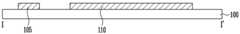
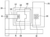
도 1은 본 발명의 실시예에 따른 박막트랜지스터를 설명하기 위한 간략한 평면도이다.
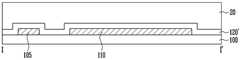
도 2는 도 1의 Ⅰ ~ Ⅰ'을 따라 절단한 단면도이다.
도 3a 내지 도 3o는 도 2의 박막트랜지스터의 제조 방법을 순차적으로 나타낸 단면도들이다.
도 4a 내지 도 4f는 도 2의 박막트랜지스터의 제조 방법을 설명하기 위한 평면도이다.
도 5a 내지 도 5o는 본 발명의 다른 실시예에 따른 박막트랜지스터의 제조 방법을 순차적으로 나타낸 단면도들이다.1 is a simplified plan view illustrating a thin film transistor according to an embodiment of the present invention.
2 is a cross-sectional view taken along the line I-I 'of FIG.
3A to 3O are sectional views sequentially illustrating a method of manufacturing the thin film transistor of FIG.
4A to 4F are plan views illustrating a method of manufacturing the thin film transistor of FIG.
5A to 5O are cross-sectional views sequentially illustrating a method of manufacturing a thin film transistor according to another embodiment of the present invention.
기타 실시예들의 구체적인 사항들은 상세한 설명 및 도면들에 포함되어 있다.The details of other embodiments are included in the detailed description and drawings.
본 발명의 이점 및 특징, 그리고 그것들을 달성하는 방법은 첨부되는 도면과 함께 상세하게 후술되어 있는 실시예들을 참조하면 명확해질 것이다.BRIEF DESCRIPTION OF THE DRAWINGS The advantages and features of the present invention and the manner of achieving them will become apparent with reference to the embodiments described in detail below with reference to the accompanying drawings.
그러나 본 발명은 이하에서 개시되는 실시예들에 한정되는 것이 아니라 서로 다른 다양한 형태로 구현될 수 있으며, 단지 본 실시예들은 본 발명의 개시가 완전하도록 하고, 본 발명이 속하는 기술분야에서 통상의 지식을 가진 자에게 고안의 범주를 완전하게 알려주기 위해 제공되는 것이며, 본 발명은 청구항의 범주에 의해 정의될 뿐이다. 명세서 전체에 걸쳐 동일 참조 부호는 동일 구성요소를 지칭한다.The present invention may, however, be embodied in many different forms and should not be construed as limited to the embodiments set forth herein. Rather, these embodiments are provided so that this disclosure will be thorough and complete, and will fully convey the scope of the invention to those skilled in the art. To fully disclose the scope of the invention to those skilled in the art, and the invention is only defined by the scope of the claims. Like reference numerals refer to like elements throughout the specification.
또한, 본 발명을 명확하게 설명하기 위해서 설명과 관계없는 부분은 생략하였으며, 도면에서 나타난 각 구성의 크기 및 두께는 설명의 편의를 위해 임의로 나타내었으므로 본 발명이 반드시 도시된 바에 한정되지 않는다.In the drawings, the same reference numbers are used throughout the drawings to refer to the same or like parts. FIG.
도면에서 여러 층 및 영역을 명확하게 표현하기 위하여 두께를 확대하여 나타내었다. 그리고 도면에서 설명의 편의를 위해 일부 층 및 영역의 두께를 과장되게 나타내었다. 층, 막, 영역, 판 등의 부분이 다른 부분 "위에" 또는 "상에" 있다고 할 때, 이는 다른 부분 "바로 위에" 있는 경우뿐 아니라 그 중간에 또 다른 부분이 있는 경우도 포함한다.In the drawings, the thickness is enlarged to clearly represent the layers and regions. The thickness of some layers and regions is exaggerated for convenience of explanation in the drawings. Whenever a portion such as a layer, film, region, plate, or the like is referred to as being "on" or "on" another portion, it includes not only the case where it is "directly on" another portion but also the case where there is another portion in between.
도 1은 본 발명의 실시예에 따른 박막트랜지스터를 설명하기 위한 간략한 평면도이고, 도 2는 도 1의 Ⅰ ~ Ⅰ'을 따라 절단한 단면도이다.FIG. 1 is a simplified plan view illustrating a thin film transistor according to an embodiment of the present invention, and FIG. 2 is a cross-sectional view taken along a line I-I 'of FIG.
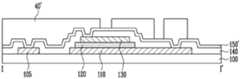
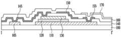
도 1 및 도 2를 참고하면, 본 발명의 실시예에 따른 박막트랜지스터는 기판(100) 상에서 수직 방향으로 연장된 바(bar) 형태의 제1 전극(105)과, 바(bar) 형태의 제1 전극(105)과 일정 간격 이격된 제2 전극(110)과, 제2 전극(110) 상에 형성된 산화물 반도체 패턴(120)과, 산화물 반도체 패턴(120) 상에 형성된 제3 전극(130)과, 제3 전극(130) 상에 형성된 제1 절연층(140)과, 제1 절연층(140) 상에 형성된 제1 및 제2 연결 패턴(145, 155)/게이트 전극(150)과, 제1 및 제2 연결 패턴(145, 155)/게이트 전극(150) 상에 형성된 제2 절연층(160) 및 제2 절연층(160) 상에 형성되어 제2 전극(110)과 전기적으로 접속되는 화소 전극(170)을 포함한다.Referring to FIGS. 1 and 2, a thin film transistor according to an embodiment of the present invention includes a
이러한 박막트랜지스터는 세로형(vertical) 타입으로 구성된다.Such a thin film transistor is configured as a vertical type.
기판(100)은 소자를 형성하기 위한 재료로 기계적 강도나 치수 안정성이 우수한 것을 선택할 수 있다. 기판(100)의 재료로는 유리판, 금속판, 세라믹판 또는 플라스틱(폴리카보네이트 수지, 폴리에스테르 수지, 에폭시 수지, 실리콘 수지, 불소 수지 등) 등을 예로 들 수 있으나, 이에 한정되지 않는다.The
제2 전극(110)은 박막트랜지스터의 소스 전극 및 드레인 전극의 한쪽으로서 기능한다. 제2 전극(110)과 일정 간격 이격된 바(bar) 형태의 제1 전극(105)은 외부로부터 제공된 전기적 신호를 제1 연결 패턴(145)을 통해 제3 전극(130)으로 제공한다.The
제1 전극(105) 및 제2 전극(110)은 알루미늄(Al)과 알루미늄 합금 등 알루미늄 계열의 금속, 은(Ag)과 은 합금 등 은 계열의 금속, 몰리브덴(Mo), 몰리브덴 합금 등 몰리브덴 계열의 금속 등의 금속성 재료로 이루어질 수 있다.The
제3 전극(130)은 박막트랜지스터의 소스 전극 및 드레인 전극의 다른 한쪽으로서 기능을 하며 제2 전극(110)과 상이한 도전 물질로 형성될 수 있다. 예를 들어, 제3 전극(130)은 구리(Cu)를 포함한 구리 계열의 금속으로 구성될 수 있다.The
산화물 반도체 패턴(120)은 산화물 반도체 물질을 포함할 수 있다. 산화물 반도체 물질은 금속 산화물 반도체로서, 아연(Zn), 인듐(In), 갈륨(Ga), 주석(Sn), 티타늄(Ti) 등의 금속의 산화물 또는 아연(Zn), 인듐(In), 갈륨(Ga), 주석(Sn), 티타늄(Ti) 등의 금속과 이들의 산화물의 조합으로 이루어질 수 있다. 예를 들어, 산화물 반도체 물질은 산화아연(ZnO), 아연-주석 산화물(ZTO), 아연-인듐 산화물(ZIO), 인듐 산화물(InO), 티타늄산화물(TiO), 인듐-갈륨-아연 산화물(IGZO), 인듐-주석-아연 산화물(ITZO) 중 적어도 하나를 포함할 수 있다.The
본 발명의 실시예에서 산화물 반도체 물질은 인듐-주석-아연 산화물(ITZO)로 이루어진 것이 바람직할 수 있다.In an embodiment of the present invention, the oxide semiconductor material may be preferably made of indium-tin-zinc oxide (ITZO).
산화물 반도체 패턴(120)의 두께(①)는 100Å 이상이 될 수 있다.The thickness (1) of the
이러한 산화물 반도체 패턴(120)은 수소화 비정질 규소에 비하여 전하의 유효 이동도(effective mobility)가 2 내지 100배 정도 크고, 온/오프 전류비가 105 내지 108의 값을 가짐으로써 뛰어난 반도체 특성을 가질 수 있다. 또한, 산화물 반도체 패턴(120)은 비정질 상태이지만 높은 전하의 유효 이동도를 가지고 있고, 기존 비정질 규소의 제조 공정을 거의 그대로 적용할 수 있어 제조 공정상 유리할 수 있다.The
제2 및 제3 전극(110, 130)은 산화물 반도체 패턴(120)을 중심으로 그 하부 및 상부에 각각 형성되어 산화물 반도체 패턴(120)과 함께 적층(계단형) 구조를 형성한다.The second and
산화물 반도체 패턴(120)이 가운데에 위치하고, 그 하부 및 상부에 각각 제2 전극(110)과 제3 전극(130)이 위치한 계단형 구조를 형성함에 따라 수직 방향으로 짧은 길이의 채널 영역이 형성될 수 있다. 이로 인해, 산화물 반도체 패턴(120)의 전체에 걸쳐 채널 영역이 형성되어 보다 많은 전류를 흘릴 수 있다.The
본 발명의 실시예에 따른 박막트랜지스터의 채널 영역은 산화물 반도체 패턴(120)의 두께(①)로 결정될 수 있다.The channel region of the thin film transistor according to the embodiment of the present invention may be determined as the thickness (1) of the
또한, 적층 구조로 이루어진 산화물 반도체 패턴(120)의 측면과 제3 전극(130)의 측면 간의 오프 셋(off set)에 의한 영역(②)으로 전류 패스가 형성되어 오프 셋(off set)에 의한 영역(②)이 채널 영역으로 확장될 수 있다. 이러한 오프 셋(off set)에 의한 영역(②)으로 인해 박막트랜지스터에서 안정성을 위해 필요한 최소한의 채널 영역을 확보할 수 있으므로 채널 영역을 위한 공정 마진이 향상될 수 있다.In addition, a current path is formed in the region (2) by offset between the side surface of the
따라서, 본 발명의 실시예에 따른 박막트랜지스터는 채널 영역이 산화물 반도체 패턴(120)의 두께(①)뿐 아니라, 산화물 반도체 패턴(120)과 제3 전극(130)의 오프 셋(off set)에 의한 영역(②)으로 확장되어 전기적 특성을 향상시킬 수 있다. 오프 셋(off set)에 의한 영역(②)은 제3 전극(130)의 측면과 산화물 반도체 패턴(120)의 측면 사이의 이격된 거리를 의미한다.Therefore, the channel region of the thin film transistor according to the embodiment of the present invention is not only the thickness (1) of the
또한, 박막트랜지스터의 채널 특성은 산화물 반도체 패턴(120)의 두께(①) 및 오프 셋(off set)에 의한 영역(②)을 통해 독립적으로 제어할 수 있다.In addition, the channel characteristics of the thin film transistor can be controlled independently through the thickness (1) of the
이때, 산화물 반도체 패턴(120)과 제3 전극(130)의 오프 셋(off set)에 의한 영역(②)은 대략 100Å 이상의 길이가 될 수 있다.At this time, the region (2) formed by offset of the
제1 절연층(140)은 제3 전극(130)이 형성된 기판(100) 전면에 형성된다. 제1 절연층(140)은 질화규소 또는 산화규소로 이루어진 무기물, 평탄화 특성이 우수하며 감광성을 가지는 유기물 또는 플라즈마 화학 기상 증착(plasma enhanced chemical vapor deposition, PECVD)으로 형성되는 a-Si:C:O, a-Si:O:F 등의 저유전율 절연 물질 등으로 이루어질 수 있다. 또한, 제1 절연층(140)은 비록 도시하지 않았으나 하부 무기막과 상부 유기막의 이중막 구조를 가질 수도 있다.The first insulating
제1 절연층(140)은 바(bar) 형태의 제1 전극(105)의 일부, 제3 전극(130)의 일부 및 제2 전극(110)의 일부를 외부로 노출하는 다수의 제1 컨택홀(H1)을 포함한다.The first insulating
게이트 전극(150)은 제2 및 제3 전극(110, 130) 및 산화물 반도체 패턴(120)과 함께 세로형(vertical) 박막트랜지스터를 구성한다. 이와 같은 게이트 전극(150)은 알루미늄(Al), 은(Ag), 구리(Cu), 몰리브덴(Mo), 크롬(Cr), 탄탈륨(Ta), 티타늄(Ti) 등의 금속 또는 이들의 합금 등으로 만들어질 수 있다.The
게이트 전극(150)은 제1 절연층(140)을 매개로 하여 산화물 반도체 패턴(120)의 측변에 형성될 수 있다.The
제1 연결 패턴(145)은 게이트 전극(150)과 동일한 레이어 상에 형성되며 게이트 전극(150)과 동일 물질로 구성되며 제1 컨택홀(H1)을 통해 제1 전극(105)과 제3 전극(130)을 전기적으로 연결한다.The
제2 연결 패턴(155)은 제1 연결 패턴(145)과 마찬가지로, 게이트 전극(150)과 동일한 레이어 상에서 동일한 물질로 구성되며 제1 컨택홀(H1)을 통해 외부로 노출된 제2 전극(110) 상에 형성되어 화소 전극(170)과 제2 전극(110)을 전기적으로 연결한다.The
제2 절연층(160)은 제1 및 제2 연결 패턴(145, 155)/게이트 전극(150)이 형성된 기판(100)에 위치하며 제2 연결 패턴(155)의 일부를 외부로 노출시키는 제2 컨택홀(H2)을 구비한다.The second
제2 절연층(160)이 형성된 기판(100) 상에는 화소 전극(170)이 형성될 수 있다. 화소 전극(170)은 제2 컨택홀(H2)에 의해 외부로 노출된 제2 연결 패턴(155) 상에 위치하여 제2 연결 패턴(155) 하부에 위치한 제2 전극(110)과 전기적으로 연결된다.The
제1 전극(105)으로 제공된 전기적 신호는 제1 연결 패턴(145)을 통해 제3 전극(130)으로 공급되어 산화물 반도체 패턴(120)의 채널 영역에 의해 제2 전극(110)으로 제공되고, 제2 연결 패턴(155)을 통해 최종적으로 화소 전극(170)으로 제공될 수 있다.The electrical signal provided to the
상술한 바와 같이, 본 발명의 실시예에 따른 박막트랜지스터는 산화물 반도체 패턴(120)의 두께(①)와 오프 셋(off set)에 의한 영역(②)으로 채널 영역이 결정될 수 있다. 따라서, 산화물 반도체 패턴(120)의 두께(①)와 오프 셋(off set)에 의한 영역(②)을 독립적으로 조절하여 채널 특성을 용이하게 제어할 수 있으므로, 본 발명의 실시예에 따른 박막트랜지스터의 전기적 특성을 향상시킬 수 있다.As described above, in the thin film transistor according to the embodiment of the present invention, the channel region can be determined by the thickness (1) of the
이하에서는 전술한 구조를 갖는 본 발명의 실시예에 따른 박막트랜지스터의 제조방법에 대해 설명하기로 한다.Hereinafter, a method of manufacturing a thin film transistor according to an embodiment of the present invention having the above-described structure will be described.
도 3a 내지 도 3o는 도 2의 박막트랜지스터의 제조 방법을 순차적으로 나타낸 단면도들이고, 도 4a 내지 도 4f는 도 2의 박막트랜지스터의 제조 방법을 설명하기 위한 평면도이다.3A to 3O are sectional views sequentially illustrating a method of manufacturing the thin film transistor of FIG. 2, and FIGS. 4A to 4F are plan views illustrating a method of manufacturing the thin film transistor of FIG.
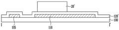
도 3a를 참고하면, 기판(100) 상에 제1 도전층(110')을 형성한다. 제1 도전층(110') 상에 제1 감광막(10)을 형성한다. 제1 도전층(110')은 알루미늄(Al)과 알루미늄 합금 등을 포함하는 알루미늄 계열의 금속, 은(Ag)과 은 합금 등을 포함하는 은 계열의 금속, 몰리브덴(Mo)과 몰리브덴 합금 등을 포함하는 몰리브덴 계열의 금속 등의 금속성 재료로 이루어질 수 있다.Referring to FIG. 3A, a first conductive layer 110 'is formed on a
제1 감광막(10) 상부에 마스크(미도시)를 배치한 후, 노광 등과 같은 일련의 단위 공정을 진행하여 도 3b에 도시된 바와 같이 감광막 패턴(10')이 형성된다. 기판(100) 상에서 제1 도전층(110')의 일부는 감광막 패턴(10')이 형성되지 않아 외부로 노출된다.After a mask (not shown) is disposed on the
이어, 도 3c 및 도 4a를 참고하면, 감광막 패턴(10')을 식각 마스크로 하여 외부로 노출된 제1 도전층(110')을 제거하여 바(bar) 형태의 제1 전극(105)과, 제1 전극(105)과 일정 간격 이격된 제2 전극(110)이 형성된다. 이어, 스트립 공정을 통해 감광막 패턴(도 3b의 110')을 제거한다.Referring to FIGS. 3C and 4A, the first conductive layer 110 'exposed to the outside is removed using the photoresist pattern 10' as an etching mask to form a
도 3d를 참고하면, 제2 전극(110)이 형성된 기판(100) 전면에 산화물 반도체 물질(120')을 증착한다. 산화물 반도체 물질(120')이 형성된 기판(100) 전면에 제2 감광막(20)을 형성한다.Referring to FIG. 3D, an oxide semiconductor material 120 'is deposited on the entire surface of the
산화물 반도체 물질(120')은 금속 산화물 반도체로서, 아연(Zn), 인듐(In), 갈륨(Ga), 주석(Sn), 티타늄(Ti) 등의 금속의 산화물 또는 아연(Zn), 인듐(In), 갈륨(Ga), 주석(Sn), 티타늄(Ti) 등의 금속과 이들의 산화물의 조합으로 이루어질 수 있다. 예를 들어, 산화물 반도체 물질은 산화 아연(ZnO), 아연-주석 산화물(ZTO), 아연-인듐 산화물(ZIO), 인듐 산화물(InO), 티타늄 산화물(TiO), 인듐-갈륨 아연 산화물(IGZO), 인듐-주석-아연 산화물(ITZO) 중 적어도 하나를 포함할 수 있다.The oxide semiconductor material 120 'is a metal oxide semiconductor and may be an oxide of a metal such as zinc (Zn), indium (In), gallium (Ga), tin (Sn), or titanium (Ti) In, gallium (Ga), tin (Sn), titanium (Ti) and oxides thereof. For example, the oxide semiconductor material may be selected from the group consisting of zinc oxide (ZnO), zinc-tin oxide (ZTO), zinc-indium oxide (ZIO), indium oxide (InO), titanium oxide (TiO), indium- gallium zinc oxide (IGZO) , And indium-tin-zinc oxide (ITZO).
제2 감광막(20) 상부에 마스크(미도시)를 배치한 후, 노광 등과 같은 일련의 단위 공정을 진행하여 도 3e에 도시된 바와 같이 감광막 패턴(20')이 형성된다. 기판(100) 상에서 산화물 반도체 물질(120')의 일부는 감광막 패턴(20')이 형성되지 않아 외부로 노출된다.After a mask (not shown) is disposed on the
도 3f 및 도 4b를 참고하면, 감광막 패턴(20)을 식각 마스크로 하여 외부로 노출된 산화물 반도체 물질(120')을 제거하여 산화물 반도체 패턴(120)이 형성된다. 이때, 식각 공정에서의 식각액은 금속 산화물 반도체 물질만 식각하는 식각액을 사용하며 산화물 반도체 물질(120') 하부에 위치한 제1 전극(105) 및 제2 전극(110)에는 영향을 미치지 않는다.Referring to FIGS. 3F and 4B, the
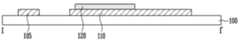
도 3g를 참고하면, 산화물 반도체 패턴(120)이 형성된 기판(100) 상에 제2 도전층(130')을 형성한다. 제2 도전층(130') 상에 제3 감광막(30)을 형성한다. 제2 도전층(130')은 제2 전극(110)과 상이한 도전 물질로 구리(Cu)를 포함한 구리 계열의 금속으로 구성될 수 있다.Referring to FIG. 3G, a second conductive layer 130 'is formed on the
제3 감광막(30) 상부에 마스크(미도시)를 배치한 후, 노광 등과 같은 일련의 단위 공정을 진행하여 도 3h에 도시된 바와 같이 감광막 패턴(30')이 형성된다. 기판(100) 상에서 제2 도전층(130')의 일부는 감광막 패턴(30')이 형성되지 않아 외부로 노출된다.After a mask (not shown) is disposed on the third
도 3i 및 도 4c를 참고하면, 감광막 패턴(30')을 식각 마스크로 하여 외부로 노출된 제2 도전층(130')을 제거하여 산화물 반도체 패턴(120)과 중첩되는 제3 전극(130)이 형성된다. 식각 공정에서의 식각액은 구리 계열의 금속으로 구성된 제2 도전층(130')만을 식각하는 식각액을 사용하며 제2 도전층(130') 하부에 위치한 산화물 반도체 패턴(120)에는 영향을 미치지 않는다.Referring to FIGS. 3I and 4C, the second conductive layer 130 'exposed to the outside is removed using the photoresist pattern 30' as an etching mask to form a
이때, 기판(100) 상에서 순차적으로 형성된 제2 전극(110), 산화물 반도체 패턴(120) 및 제3 전극(130)은 계단형의 적층 구조를 갖는다. 산화물 반도체 패턴(120)이 가운데에 위치하고 그 하부 및 상부에 각각 제2 전극(110) 및 제3 전극(130)이 위치함에 따라 수직 방향으로 길이를 갖는 채널 영역이 형성된다.At this time, the
또한, 계단형의 적층 구조로 이루어진 산화물 반도체 패턴(120)의 측면과 제3 전극(130)의 측면 간의 오프 셋(off set)에 의한 영역으로 전류 패스가 형성된다.Further, a current path is formed in an area offset between a side surface of the
도 3j 및 도 4d를 참고하면, 제3 전극(130)이 형성된 기판(100) 상에 제1 전극(105)의 일부, 제2 전극(110)의 일부 및 제3 전극(130)의 일부를 각각 외부로 노출하는 다수의 제1 컨택홀(H1)을 구비한 제1 절연층(140)이 형성된다.3J and 4D, a part of the
이어, 도 3k를 참고하면, 제1 절연층(140)이 형성된 기판(100) 상에 제3 도전층(150')을 형성한다. 제3 도전층(150')이 형성된 기판(100) 전면에 제4 감광막(40)을 형성한다. 제3 도전층(150')은 알루미늄(Al), 은(Ag), 구리(Cu), 몰리브덴(Mo), 크롬(Cr), 탄탈륨(Ta), 티타늄(Ti) 등의 금속 또는 이들의 합금 등으로 만들어질 수 있다.Referring to FIG. 3K, a third conductive layer 150 'is formed on the
제4 감광막(40) 상부에 마스크(미도시)를 배치한 후, 노광 등과 같은 일련의 단위 공정을 진행하여 도 3l에 도시된 바와 같이 감광막 패턴(40')이 형성된다. 기판(100) 상에서 제3 도전층(150')의 일부는 감광막 패턴(40')이 형성되지 않아 외부로 노출된다.After a mask (not shown) is disposed on the
도 3m 및 도 4e를 참고하면, 감광막 패턴(40')을 식각 마스크로 하여 외부로 노출된 제3 도전층(130)을 제거하여 제1 컨택홀(도 3j의 H1)을 통해 제1 전극(105)과 제3 전극(130)을 전기적으로 연결하는 제1 연결패턴(145) 및 산화물 반도체 패턴(120)의 측변에 위치한 게이트 전극(150)이 형성된다.Referring to FIGS. 3M and 4E, the third
또한, 제1 컨택홀(H1)을 통해 제2 전극(110)의 일부와 접속되는 제2 연결 패턴(155)이 형성된다.Also, a
제1 연결 패턴(145)은 외부로부터 제1 전극(105)으로 제공되는 전기적 신호를 제2 전극(130)으로 전달한다. 제2 전극(130)으로 전달된 전기적 신호는 그 하부에 형성된 산화물 반도체 패턴(120)의 채널 영역에 의해 산화물 반도체 패턴(120) 하부에 형성된 제2 전극(110)으로 제공될 수 있다.The
도 3n을 참고하면, 제1 및 제2 연결 패턴(145, 155)과 게이트 전극(150)이 형성된 기판(100) 상에 제2 연결 패턴(155)의 일부를 외부로 노출하는 제2 컨택홀(H2)을 구비한 제2 절연층(160)이 형성된다.Referring to FIG. 3N, on the
연속하여, 도 3o 및 도 4f를 참고하면, 제2 절연층(160)이 형성된 기판(100) 상에 제2 컨택홀(H2)을 통해 제2 연결 패턴(155)에 접속되는 화소 전극(170)이 형성된다. 화소 전극(170)은 투명 도전 물질로 이루어질 수 있다. 투명 도전 물질로는 인듐 주석 산화물(ITO), 인듐 아연 산화물(IZO), 징크옥사이드(ZnO), In2O3 등과 같은 산화물 계열의 투명 도전막을 포함할 수 있다.3O and 4F, a
제2 전극(110)으로 제공된 전기적 신호는 제2 연결 패턴(155)과 직접적으로 접속된 화소 전극(170)으로 최종적으로 제공된다.The electrical signal provided to the
상술한 본 발명의 실시예에 따르면, 박막트랜지스터의 채널 영역이 산화물 반도체 패턴(120)의 두께와 산화물 반도체 패턴(120)과 제3 전극(130) 간의 오프 셋(off set)에 의한 영역으로 제어됨에 따라 위의 두 가지 요소를 독립적으로 조절하여 박막트랜지스터의 전기적 특성을 향상시킬 수 있다.The channel region of the thin film transistor is controlled by controlling the thickness of the
도 5a 내지 도 5o는 본 발명의 다른 실시예에 따른 박막트랜지스터의 제조 방법을 순차적으로 나타낸 단면도들이다. 상술한 실시예와 동일한 구성요소의 설명은 생략하며 차이점을 중심으로 설명한다.5A to 5O are cross-sectional views sequentially illustrating a method of manufacturing a thin film transistor according to another embodiment of the present invention. The description of the same components as those of the above-described embodiment will be omitted and differences will be mainly described.
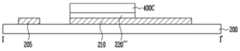
도 5a를 참고하면, 기판(200) 상에 순차적으로 제1 도전층(210')과 산화물 반도체 물질(220')을 형성한다. 산화물 반도체 물질(220') 상에 제1 감광막(400)을 형성한다. 제1 감광막(400) 상부에 반투과부(A), 투과부(B) 및 차단부(C)를 구비한 하프톤 마스크(300)를 배치한 후 노광 등의 일련의 단위 공정을 포함하는 마스크 공정을 진행하여 도 5b에 도시된 바와 같이 서로 상이한 두께를 갖는 제1 및 제2 감광막 패턴(400a, 400b)을 형성한다.Referring to FIG. 5A, a first conductive layer 210 'and an oxide semiconductor material 220' are sequentially formed on a
제1 감광막 패턴(400a)은 하프톤 마스크(300)의 반투과부(A)에 대응되어 형성되고 제1 두께를 갖는다. 제2 감광막 패턴(400b)은 하프톤 마스크(300)의 차단부(C)에 대응되어 형성되고 제1 두께보다 두꺼운 제2 두께를 갖는다.The
또한, 기판(200) 상에서 하프톤 마스크(300)의 투과부(B)에 대응되는 제1 감광막(400)은 제거되어 그 하부에 위치한 산화물 반도체 물질(220')이 외부로 노출된다.In addition, the
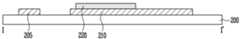
도 5c를 참고하면, 제1 및 제2 감광막 패턴(400a, 400b)을 식각 마스크로 하여 기판(200) 상에 형성된 제1 도전층(210') 및 산화물 반도체 물질(220')의 식각 공정을 진행한다. 제1 도전층(210') 및 산화물 반도체 물질(220')은 일괄 식각된다.Referring to FIG. 5C, the first conductive layer 210 'and the oxide semiconductor material 220', which are formed on the
이러한 식각 공정에 의해 제1 도전층(210')은 제1 전극(205)과, 제1 전극(205)과 일정 간격 이격된 제2 전극(210)으로 패터닝되고, 산화물 반도체 물질(220')은 제1 및 제2 감광막 패턴(400a, 400b)과 대응되는 영역에만 위치한 제1 산화물 반도체 물질층(220")으로 패터닝된다.The first
도 5d를 참고하면, 에치 백(etch back)과 같은 화학 처리를 진행하여, 제1 감광막 패턴(400a)을 제거하여 제1 산화물 반도체 물질층(220')을 외부로 노출시킨다. 이와 동시에, 후술한 제3 전극이 형성될 위치에 배치된 제2 감광막 패턴(도 5c의 400a)의 두께보다 얇아진 제3 감광막 패턴(400c)이 형성된다.Referring to FIG. 5D, a chemical treatment such as an etch back is performed to expose the first oxide semiconductor material layer 220 'to the outside by removing the
도 5e를 참고하면, 제3 감광막 패턴(400c)을 식각 마스크로 하여 습식 식각(wet etch) 공정을 진행하여 외부로 노출된 제1 산화물 반도체 물질층(220')을 제거하여 바(bar) 형태의 제1 전극(205) 및 제2 전극(210)의 일부를 외부로 노출시킨다. 또한, 스트립 공정을 통해 제3 감광막 패턴(400c)을 제거하여 도 5f에 도시된 바와 같이, 제2 전극(210) 상에 산화물 반도체 패턴(220)이 형성된다.Referring to FIG. 5E, a wet etch process is performed using the third photoresist pattern 400c as an etch mask to remove the first exposed oxide semiconductor material layer 220 'to form a bar shape A part of the
이와 같이, 기판(200) 상에서 박막트랜지스터를 구성하는 제2 전극(210) 및 산화물 반도체 패턴(220)은 하나의 마스크 공정으로 형성될 수 있다.As described above, the
도 5g를 참고하면, 산화물 반도체 패턴(220)이 형성된 기판(200) 상에 제2 도전층(230')을 형성한다. 제2 도전층(230') 상에 제2 감광막(500)을 형성한다. 제2 감광막(500) 상부에 마스크(미도시)를 배치한 후, 노광 등과 같은 일련의 단위 공정을 진행하여 도 5h에 도시된 바와 같이 감광막 패턴(500')이 형성된다. 기판(200) 상에서 제2 도전층(230')의 일부는 감광막 패턴(500')이 형성되지 않아 외부로 노출된다.Referring to FIG. 5G, a second conductive layer 230 'is formed on the
도 5i를 참고하면, 감광막 패턴(500')을 식각 마스크로 하여 외부로 노출된 제2 도전층(230')을 제거하여 산화물 반도체 패턴(220)과 중첩되는 제3 전극(230)이 형성된다.Referring to FIG. 5I, the second conductive layer 230 'exposed to the outside is removed using the photoresist pattern 500' as an etching mask to form a
이때, 기판(200) 상에서 순차적으로 형성된 제2 전극(210), 산화물 반도체 패턴(220) 및 제3 전극(230)은 계단형의 적층 구조를 갖는다. 산화물 반도체 패턴(220)이 가운데에 위치하고 그 하부 및 상부에 각각 제2 전극(210) 및 제3 전극(230)이 위치함에 따라 수직 방향으로 길이를 갖는 채널 영역이 형성된다.At this time, the
또한, 계단형의 적층 구조로 이루어진 산화물 반도체 패턴(220)의 측면과 제3 전극(230)의 측면 간의 오프 셋(off set)에 의한 영역으로 전류 패스가 형성된다.Further, a current path is formed in an area offset between a side surface of the
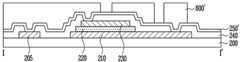
도 5j를 참고하면, 제3 전극(230)이 형성된 기판(200) 상에 제1 전극(205)의 일부, 제2 전극(210)의 일부 및 제3 전극(230)의 일부를 각각 외부로 노출하는 다수의 제1 컨택홀(H1)을 구비한 제1 절연층(240)이 형성된다.5J, a part of the
이어, 도 5k를 참고하면, 제1 절연층(240)이 형성된 기판(200) 상에 제3 도전층(250')을 형성한다. 제3 도전층(250')이 형성된 기판(200) 전면에 제3 감광막(600)을 형성한다.Referring to FIG. 5K, a third conductive layer 250 'is formed on the
제3 감광막(600) 상부에 마스크(미도시)를 배치한 후, 노광 등과 같은 일련의 단위 공정을 진행하여 도 5l에 도시된 바와 같이 감광막 패턴(600')이 형성된다. 기판(200) 상에서 제3 도전층(250')의 일부는 감광막 패턴(600')이 형성되지 않아 외부로 노출된다.After a mask (not shown) is disposed on the
도 5m을 참고하면, 감광막 패턴(600')을 식각 마스크로 하여 외부로 노출된 제3 도전층(250')을 제거하여 제1 컨택홀(도 5j의 H1)을 통해 제1 전극(205)과 제3 전극(230)을 전기적으로 연결하는 제1 연결 패턴(245) 및 산화물 반도체 패턴(220)의 측변에 위치한 게이트 전극(250)이 형성된다.Referring to FIG. 5M, the third conductive layer 250 'exposed to the outside is removed using the photoresist pattern 600' as an etching mask to form the
또한, 제1 컨택홀(H1)을 통해 제2 전극(210)의 일부와 접속되는 제2 연결 패턴(255)이 형성된다.In addition, a
제1 연결 패턴(245)은 외부로부터 제1 전극(205)으로 제공되는 전기적 신호를 제3 전극(230)으로 전달한다. 이로 인해, 제3 전극(230)으로 전달된 전기적 신호는 그 하부에 형성된 산화물 반도체 패턴(220)의 채널 영역에 의해 산화물 반도체 패턴(220) 하부에 형성된 제2 전극(210)으로 제공될 수 있다.The
도 5n을 참고하면, 제1 및 제2 연결 패턴(245, 255)과 게이트 전극(250)이 형성된 기판(200) 상에 제2 연결 패턴(255)의 일부를 외부로 노출하는 제2 컨택홀(H2)을 구비한 제2 절연층(260)이 형성된다.5n, a second contact hole 252 for exposing a part of the
연속하여, 도 5o를 참고하면, 제2 절연층(260)이 형성된 기판(200) 상에 제2 컨택홀(H2)을 통해 제2 연결 패턴(255)에 접속된 화소 전극(270)이 형성된다.5O, a
본 발명이 속하는 기술분야의 상의 지식을 가진 자는 본 발명이 그 기술적 사상이나 필수적인 특징을 변경하지 않고서 다른 구체적인 형태로 실시될 수 있다는 것을 이해할 수 있을 것이다. 그러므로 이상에서 기술한 실시예들은 모든 면에서 예시적인 것이며 한정적이 아닌 것으로 이해해야만 한다. 본 발명의 범위는 상기 상세한 설명보다는 후술하는 특허 청구범위에 의하여 나타내어지며 특히 청구범위의 의미 및 범위 그리고 균등 개념으로부터 도출되는 모든 변경 또는 변형된 형태가 본 발명의 범위에 포함되는 것으로 해석되어야 한다.It will be understood by those skilled in the art that the present invention may be embodied in other specific forms without departing from the spirit or essential characteristics thereof. It is therefore to be understood that the above-described embodiments are illustrative in all aspects and not restrictive. The scope of the present invention is defined by the appended claims rather than the detailed description, and all changes or modifications derived from the meaning and scope of the claims and the equivalents should be construed as being included within the scope of the present invention.
100/200: 기판105/205: 제1 전극
110/210; 제2 전극120/220: 산화물 반도체 패턴
130/230: 제3 전극140/240: 제1 절연층
145/245: 제1 연결 패턴150/250: 게이트 전극
155/255: 제2 연결 패턴160/260: 제2 절연층
170/270: 화소 전극100/200:
110/210;
130/230:
145/245:
155/255:
170/270:
Claims (18)
Translated fromKorean상기 기판 상에 위치하는 제1 전극과, 상기 제1 전극과 일정 간격 이격된 제2 전극;
상기 제2 전극 상에 위치하며 채널 영역을 포함한 산화물 반도체 패턴;
상기 산화물 반도체 패턴 상에 위치하는 제3 전극;
상기 제3 전극을 포함한 기판에 위치하며 상기 제1 전극의 일부, 상기 제2 전극의 일부 및 상기 제3 전극의 일부를 각각 노출하는 제1 컨택홀을 구비한 제1 절연층;
상기 제1 절연층 상에 위치하며 상기 산화물 반도체 패턴의 일부와 대응된 게이트 전극;
상기 게이트 전극을 포함한 기판에 위치하며 상기 제2 전극의 일부를 노출하는 제1 컨택홀과 대응되는 제2 컨택홀을 구비한 제2 절연층; 및
상기 제2 절연층 상에 위치하여 상기 제1 및 제2 컨택홀을 통해 상기 제2 전극과 전기적으로 접속되는 화소 전극을 포함하는 박막트랜지스터.Board;
A first electrode disposed on the substrate; a second electrode spaced apart from the first electrode by a predetermined distance;
An oxide semiconductor pattern located on the second electrode and including a channel region;
A third electrode located on the oxide semiconductor pattern;
A first insulating layer located on the substrate including the third electrode and having a first contact hole exposing a part of the first electrode, a part of the second electrode and a part of the third electrode, respectively;
A gate electrode located on the first insulating layer and corresponding to a part of the oxide semiconductor pattern;
A second insulating layer located on the substrate including the gate electrode and having a second contact hole corresponding to a first contact hole exposing a part of the second electrode; And
And a pixel electrode located on the second insulating layer and electrically connected to the second electrode through the first and second contact holes.
상기 제2 전극 및 제3 전극은 상기 산화물 반도체 패턴의 하부 및 상부에 각각 위치함으로써, 적층구조를 형성하는 박막트랜지스터.The method according to claim 1,
And the second electrode and the third electrode are respectively located below and above the oxide semiconductor pattern, thereby forming a laminated structure.
상기 제2 전극 및 제3 전극은 서로 상이한 금속 물질을 포함하는 박막트랜지스터.The method according to claim 1,
Wherein the second electrode and the third electrode comprise different metal materials.
상기 산화물 반도체 패턴은 인듐-주석-아연 산화물(Indium-Tin-Zinc-Oxide, ITZO)을 포함하는 박막트랜지스터.The method according to claim 1,
Wherein the oxide semiconductor pattern comprises indium-tin-zinc-oxide (ITZO).
상기 채널영역은 상기 제3 전극과 상기 산화물 반도체 패턴 사이의 오프 셋(off set)에 의한 영역 및 상기 산화물 반도체 패턴의 두께로 결정되는 박막트랜지스터.The method according to claim 1,
Wherein the channel region is determined by an off-set region between the third electrode and the oxide semiconductor pattern and a thickness of the oxide semiconductor pattern.
상기 제1 절연층 상에 위치하여 상기 제1 컨택홀을 통해 상기 제1 전극과 상기 제3 전극을 전기적으로 연결하는 연결 패턴을 더 포함하는 박막트랜지스터.The method according to claim 1,
And a connection pattern located on the first insulating layer and electrically connecting the first electrode and the third electrode through the first contact hole.
상기 연결 패턴은 상기 게이트 전극과 동일한 레이어에서 동일한 물질을 포함하는 박막트랜지스터.The method according to claim 6,
Wherein the connection pattern includes the same material in the same layer as the gate electrode.
상기 제1 및 제2 전극은 동일한 레이어에서 동일한 물질을 포함하는 박막트랜지스터.The method according to claim 1,
Wherein the first and second electrodes comprise the same material in the same layer.
상기 제2 전극 상에 채널 영역을 포함한 산화물 반도체 패턴을 형성하는 단계;
상기 산화물 반도체 패턴 상에서 상기 제2 전극의 일부와 중첩되는 제3 전극을 형성하는 단계;
상기 제3 전극을 포함한 기판 상에서 상기 제1 전극의 일부와, 상기 제2 전극의 일부 및 제3 전극의 일부를 각각 노출하는 제1 컨택홀을 구비한 제1 절연층을 형성하는 단계;
상기 제1 절연층 상에서 상기 산화물 반도체 패턴의 일부와 대응된 게이트 전극을 형성함과 동시에 상기 제1 컨택홀을 통해 상기 제1 전극과 상기 제3 전극을 전기적으로 연결하는 연결 패턴을 형성하는 단계;
상기 게이트 전극 상에서 상기 제2 전극의 일부를 노출하는 제1 컨택홀과 대응되는 제2 컨택홀을 구비한 제2 절연층을 형성하는 단계; 및
상기 제2 절연층 상에서 상기 제1 및 제2 컨택홀을 통해 상기 제2 전극과 전기적으로 접속되는 화소 전극을 형성하는 단계를 포함하는 박막트랜지스터의 제조방법.Forming a first electrode on the substrate and a second electrode spaced apart from the first electrode by a predetermined distance;
Forming an oxide semiconductor pattern including a channel region on the second electrode;
Forming a third electrode on the oxide semiconductor pattern to overlap with a portion of the second electrode;
Forming a first insulating layer on the substrate including the third electrode, the first insulating layer having a first contact hole exposing a part of the first electrode, a part of the second electrode and a part of the third electrode, respectively;
Forming a gate electrode corresponding to a part of the oxide semiconductor pattern on the first insulating layer and forming a connection pattern for electrically connecting the first electrode and the third electrode through the first contact hole;
Forming a second insulating layer on the gate electrode, the second insulating layer having a first contact hole exposing a portion of the second electrode and a second contact hole corresponding to the first contact hole; And
And forming a pixel electrode electrically connected to the second electrode through the first and second contact holes on the second insulating layer.
상기 제2 전극 및 제3 전극은 상기 산화물 반도체 패턴의 하부 및 상부에 각각 위치함으로써, 적층 구조를 형성하는 박막트랜지스터의 제조방법.10. The method of claim 9,
And the second electrode and the third electrode are respectively located below and above the oxide semiconductor pattern, thereby forming a laminated structure.
상기 제2 전극 및 제3 전극은 서로 상이한 금속 물질을 포함하는 박막트랜지스터의 제조방법.10. The method of claim 9,
Wherein the second electrode and the third electrode comprise different metal materials.
상기 채널 영역은 상기 제3 전극과 상기 산화물 반도체 패턴 사이의 오프 셋(off set)에 의한 영역 및 상기 산화물 반도체 패턴의 두께로 결정되는 박막트랜지스터의 제조방법.10. The method of claim 9,
Wherein the channel region is determined by an off-set region between the third electrode and the oxide semiconductor pattern and a thickness of the oxide semiconductor pattern.
상기 산화물 반도체 패턴은 인듐-주석-아연 산화물(Indium-Tin-Zinc-Oxide, ITZO)을 포함하는 박막트랜지스터의 제조방법.10. The method of claim 9,
Wherein the oxide semiconductor pattern comprises indium-tin-zinc-oxide (ITZO).
상기 산화물 반도체층 상부에 감광막을 증착한 후 상기 감광막 상부에 마스크를 배치하여 제1 감광막 패턴과 상기 제1 감광막 패턴보다 두꺼운 제2 감광막 패턴을 형성하는 단계;
상기 제1 감광막 패턴 및 제2 감광막 패턴을 마스크로 하여 노출된 부분의 상기 산화물 반도체층 및 도전층을 일괄 식각하여 산화물 반도체 패턴, 제1 전극 및 상기 제1 전극과 일정 간격 이격된 제2 전극을 형성하는 단계;
상기 제1 감광막 패턴을 제거하여 상기 산화물 반도체 패턴을 외부로 노출시키고, 상기 제2 감광막 패턴을 두께가 얇은 제3 감광막 패턴으로 형성하는 단계;
상기 노출된 산화물 반도체 패턴을 제거하고 그 하부에 위치한 제1 전극 및 제2 전극을 외부로 노출시키는 단계;
상기 제3 감광막 패턴을 제거하고 그 하부에 위치한 제2 전극과 채널 영역을 포함한 산화물 반도체 패턴을 외부로 노출시키는 단계;
상기 산화물 반도체 패턴 상에 위치하며 상기 제2 전극의 일부와 중첩되는 제3 전극을 형성하는 단계;
상기 제3 전극 상에서 상기 제1 전극의 일부, 상기 제2 전극의 일부 및 제3 전극의 일부를 각각 노출하는 제1 컨택홀을 구비한 제1 절연층을 형성하는 단계;
상기 제1 절연층 상에서 상기 산화물 반도체 패턴의 일부와 대응되는 게이트 전극을 형성함과 동시에 상기 제1 컨택홀을 통해 상기 제1 전극과 상기 제3 전극을 전기적으로 연결하는 연결 패턴을 형성하는 단계;
상기 게이트 전극 상에서 상기 제2 전극의 일부를 노출하는 제1 컨택홀과 대응되는 제2 컨택홀을 구비한 제2 절연층을 형성하는 단계; 및
상기 제2 절연층 상에서 상기 제1 및 제2 컨택홀을 통해 상기 제2 전극과 전기적으로 접속되는 화소 전극을 형성하는 단계를 포함하는 박막트랜지스터의 제조방법.Sequentially forming a conductive layer and an oxide semiconductor layer on a substrate;
Forming a first photoresist pattern and a second photoresist pattern thicker than the first photoresist pattern by depositing a photoresist over the oxide semiconductor layer and disposing a mask on the photoresist layer;
The oxide semiconductor layer and the conductive layer of the exposed portion are etched using the first photoresist pattern and the second photoresist pattern as masks to form an oxide semiconductor pattern, a first electrode, and a second electrode spaced apart from the first electrode by a predetermined distance ;
Removing the first photoresist pattern to expose the oxide semiconductor pattern to the outside, and forming the second photoresist pattern as a third photoresist pattern having a small thickness;
Removing the exposed oxide semiconductor pattern and exposing a first electrode and a second electrode located under the exposed oxide semiconductor pattern to the outside;
Removing the third photoresist pattern and exposing an oxide semiconductor pattern including a second electrode and a channel region located under the third photoresist pattern to the outside;
Forming a third electrode on the oxide semiconductor pattern and overlapping a portion of the second electrode;
Forming a first insulating layer on the third electrode, the first insulating layer having a first contact hole exposing a part of the first electrode, a part of the second electrode and a part of the third electrode, respectively;
Forming a gate electrode corresponding to a portion of the oxide semiconductor pattern on the first insulating layer and forming a connection pattern for electrically connecting the first electrode and the third electrode through the first contact hole;
Forming a second insulating layer on the gate electrode, the second insulating layer having a first contact hole exposing a portion of the second electrode and a second contact hole corresponding to the first contact hole; And
And forming a pixel electrode electrically connected to the second electrode through the first and second contact holes on the second insulating layer.
상기 제2 전극 및 제3 전극은 상기 산화물 반도체 패턴의 하부 및 상부에 각각 위치함으로써, 적층 구조를 형성하는 박막트랜지스터의 제조방법.15. The method of claim 14,
And the second electrode and the third electrode are respectively located below and above the oxide semiconductor pattern, thereby forming a laminated structure.
상기 제2 전극 및 제3 전극은 서로 상이한 금속 물질을 포함하는 박막트랜지스터의 제조방법.15. The method of claim 14,
Wherein the second electrode and the third electrode comprise different metal materials.
상기 채널 영역은 상기 제3 전극과 상기 산화물 반도체 패턴 사이의 오프 셋(off set)에 의한 영역 및 상기 산화물 반도체 패턴의 두께로 결정되는 박막트랜지스터의 제조방법.15. The method of claim 14,
Wherein the channel region is determined by an off-set region between the third electrode and the oxide semiconductor pattern and a thickness of the oxide semiconductor pattern.
상기 산화물 반도체 패턴은 인듐-주석-아연 산화물(Indium-Tin-Zinc-Oxide, ITZO)을 포함한 박막트랜지스터의 제조방법.
15. The method of claim 14,
Wherein the oxide semiconductor pattern comprises indium-tin-zinc-oxide (ITZO).
Priority Applications (2)
| Application Number | Priority Date | Filing Date | Title |
|---|---|---|---|
| KR1020150004151AKR20160087024A (en) | 2015-01-12 | 2015-01-12 | Thin film transistor and method for fabricaing the same |
| US14/886,214US9831350B2 (en) | 2015-01-12 | 2015-10-19 | Thin film transistor and method of manufacturing the same |
Applications Claiming Priority (1)
| Application Number | Priority Date | Filing Date | Title |
|---|---|---|---|
| KR1020150004151AKR20160087024A (en) | 2015-01-12 | 2015-01-12 | Thin film transistor and method for fabricaing the same |
Publications (1)
| Publication Number | Publication Date |
|---|---|
| KR20160087024Atrue KR20160087024A (en) | 2016-07-21 |
Family
ID=56368121
Family Applications (1)
| Application Number | Title | Priority Date | Filing Date |
|---|---|---|---|
| KR1020150004151AWithdrawnKR20160087024A (en) | 2015-01-12 | 2015-01-12 | Thin film transistor and method for fabricaing the same |
Country Status (2)
| Country | Link |
|---|---|
| US (1) | US9831350B2 (en) |
| KR (1) | KR20160087024A (en) |
Cited By (1)
| Publication number | Priority date | Publication date | Assignee | Title |
|---|---|---|---|---|
| US11832486B2 (en) | 2021-09-14 | 2023-11-28 | Electronics And Telecommunications Research Institute | Semiconductor device, display panel, and display device including the same |
Families Citing this family (7)
| Publication number | Priority date | Publication date | Assignee | Title |
|---|---|---|---|---|
| WO2017145939A1 (en)* | 2016-02-24 | 2017-08-31 | シャープ株式会社 | Thin film transistor substrate and display panel |
| CN106169485B (en)* | 2016-08-31 | 2019-06-14 | 深圳市华星光电技术有限公司 | TFT array substrate, method for making the same, and display device |
| CN106298959A (en)* | 2016-11-01 | 2017-01-04 | 京东方科技集团股份有限公司 | Thin film transistor (TFT) and manufacture method, array base palte and display device |
| CN107425077B (en)* | 2017-05-17 | 2020-03-06 | 京东方科技集团股份有限公司 | Thin film transistor, method for making the same, and display device |
| CN113299741B (en) | 2021-05-07 | 2022-09-09 | 惠州市华星光电技术有限公司 | Thin film transistor device, backlight module and display panel |
| CN115188830A (en)* | 2022-07-27 | 2022-10-14 | 武汉华星光电技术有限公司 | Thin film transistor with vertical structure and electronic device |
| CN115513300A (en)* | 2022-09-27 | 2022-12-23 | 武汉华星光电技术有限公司 | Thin film transistor of vertical structure and electronic device |
Family Cites Families (15)
| Publication number | Priority date | Publication date | Assignee | Title |
|---|---|---|---|---|
| KR100870659B1 (en) | 2001-12-31 | 2008-11-26 | 엘지디스플레이 주식회사 | Liquid crystal display device manufacturing method |
| KR101000451B1 (en)* | 2004-02-05 | 2010-12-13 | 삼성전자주식회사 | Method for forming aluminum wiring of TFT LCD board and TFT LC board |
| KR101054344B1 (en)* | 2004-11-17 | 2011-08-04 | 삼성전자주식회사 | Thin film transistor array panel and manufacturing method thereof |
| KR20080007813A (en)* | 2006-07-18 | 2008-01-23 | 삼성전자주식회사 | Thin film transistor array substrate |
| KR101489652B1 (en)* | 2008-09-02 | 2015-02-06 | 삼성디스플레이 주식회사 | Thin film transistor substrate and manufacturing method thereof |
| JP5796760B2 (en)* | 2009-07-29 | 2015-10-21 | Nltテクノロジー株式会社 | Transistor circuit |
| WO2011034012A1 (en)* | 2009-09-16 | 2011-03-24 | Semiconductor Energy Laboratory Co., Ltd. | Logic circuit, light emitting device, semiconductor device, and electronic device |
| WO2011065244A1 (en) | 2009-11-28 | 2011-06-03 | Semiconductor Energy Laboratory Co., Ltd. | Semiconductor device and method for manufacturing the same |
| KR20120014380A (en) | 2010-08-09 | 2012-02-17 | 삼성전자주식회사 | Vertical oxide semiconductor and method of manufacturing the same |
| KR20120039947A (en)* | 2010-10-18 | 2012-04-26 | 삼성모바일디스플레이주식회사 | Display device and method for manufacturing the same |
| KR101909704B1 (en)* | 2011-02-17 | 2018-10-19 | 삼성디스플레이 주식회사 | Display substrate and method of manufacturing the display substrate |
| KR20130016938A (en)* | 2011-08-09 | 2013-02-19 | 삼성디스플레이 주식회사 | Organic light emitting display device and manufacturing method of the same |
| US9312257B2 (en) | 2012-02-29 | 2016-04-12 | Semiconductor Energy Laboratory Co., Ltd. | Semiconductor device |
| JP6100071B2 (en) | 2012-04-30 | 2017-03-22 | 株式会社半導体エネルギー研究所 | Method for manufacturing semiconductor device |
| KR102227637B1 (en)* | 2013-11-07 | 2021-03-16 | 삼성디스플레이 주식회사 | Infrared detection device, infrared detection sensor having an infrared dection device and method of manufaturing the same |
- 2015
- 2015-01-12KRKR1020150004151Apatent/KR20160087024A/ennot_activeWithdrawn
- 2015-10-19USUS14/886,214patent/US9831350B2/enactiveActive
Cited By (1)
| Publication number | Priority date | Publication date | Assignee | Title |
|---|---|---|---|---|
| US11832486B2 (en) | 2021-09-14 | 2023-11-28 | Electronics And Telecommunications Research Institute | Semiconductor device, display panel, and display device including the same |
Also Published As
| Publication number | Publication date |
|---|---|
| US20160204267A1 (en) | 2016-07-14 |
| US9831350B2 (en) | 2017-11-28 |
Similar Documents
| Publication | Publication Date | Title |
|---|---|---|
| JP5324111B2 (en) | Thin film transistor array panel and manufacturing method thereof | |
| KR20160087024A (en) | Thin film transistor and method for fabricaing the same | |
| US8445301B2 (en) | Thin-film transistor substrate, method of manufacturing the same, and display device including the same | |
| US20150295092A1 (en) | Semiconductor device | |
| WO2019114834A1 (en) | Array substrate and manufacturing method thereof, and display device | |
| CN110021669B (en) | Thin film transistor, method for manufacturing the same, and display device including the same | |
| US8884286B2 (en) | Switching element, display substrate and method of manufacturing the same | |
| WO2014166176A1 (en) | Thin-film transistor and manufacturing method thereof, array base plate and display apparatus | |
| KR102080484B1 (en) | Array substrate for Liquid crystal display device and Method for manufacturing the same | |
| JP2014131047A (en) | Thin-film transistor and thin-film transistor display board | |
| US9224869B2 (en) | Semiconductor device and method for manufacturing same | |
| KR20150004536A (en) | Display substrate having a thin film transistor and method of manufacturing the same | |
| JP5991668B2 (en) | Display device and manufacturing method thereof | |
| KR20160085402A (en) | Thin film transistor substrate and method of manufacturing the same | |
| EP3261127A1 (en) | Thin-film transistor and manufacturing method therefor, array substrate and display device | |
| KR20100070082A (en) | Thin film transistor substrate and method of fabricating thereof | |
| TW201342628A (en) | Active component and method of manufacturing same | |
| KR20170072438A (en) | Transistor array panel and manufacturing method thereof | |
| KR101756659B1 (en) | Thin film transistor substrate and method for fabricating the same | |
| JP7671625B2 (en) | Semiconductor device and its manufacturing method | |
| KR102111067B1 (en) | Switching element, display substrate and method of manufacturing the same | |
| US9035364B2 (en) | Active device and fabricating method thereof | |
| KR20150061256A (en) | Display substrate comprising pixel tft and driving tft and preparation method thereof | |
| KR20140081413A (en) | Thin film transistor array panel and manufacturing method thereof | |
| KR102197263B1 (en) | Display substrate having a thin film transistor and method of manufacturing the same |
Legal Events
| Date | Code | Title | Description |
|---|---|---|---|
| PA0109 | Patent application | Patent event code:PA01091R01D Comment text:Patent Application Patent event date:20150112 | |
| PG1501 | Laying open of application | ||
| PC1203 | Withdrawal of no request for examination | ||
| WITN | Application deemed withdrawn, e.g. because no request for examination was filed or no examination fee was paid |