KR20160087021A - Display appratus - Google Patents
Display appratusDownload PDFInfo
- Publication number
- KR20160087021A KR20160087021AKR1020150004129AKR20150004129AKR20160087021AKR 20160087021 AKR20160087021 AKR 20160087021AKR 1020150004129 AKR1020150004129 AKR 1020150004129AKR 20150004129 AKR20150004129 AKR 20150004129AKR 20160087021 AKR20160087021 AKR 20160087021A
- Authority
- KR
- South Korea
- Prior art keywords
- light
- light source
- display
- panel
- electrode
- Prior art date
- Legal status (The legal status is an assumption and is not a legal conclusion. Google has not performed a legal analysis and makes no representation as to the accuracy of the status listed.)
- Ceased
Links
- 239000000758substrateSubstances0.000claimsabstractdescription52
- 239000000463materialSubstances0.000claimsdescription25
- 238000000034methodMethods0.000claimsdescription21
- 239000004973liquid crystal related substanceSubstances0.000claimsdescription18
- 230000003287optical effectEffects0.000claimsdescription14
- 239000011159matrix materialSubstances0.000claimsdescription13
- 239000003086colorantSubstances0.000claimsdescription6
- 239000010410layerSubstances0.000description70
- 239000010408filmSubstances0.000description10
- 238000009792diffusion processMethods0.000description7
- 239000002356single layerSubstances0.000description5
- 239000007983Tris bufferSubstances0.000description4
- XLOMVQKBTHCTTD-UHFFFAOYSA-NZinc monoxideChemical compound[Zn]=OXLOMVQKBTHCTTD-UHFFFAOYSA-N0.000description4
- 229910052782aluminiumInorganic materials0.000description4
- 239000002019doping agentSubstances0.000description4
- 229920000139polyethylene terephthalatePolymers0.000description4
- 239000005020polyethylene terephthalateSubstances0.000description4
- 239000004065semiconductorSubstances0.000description4
- XAGFODPZIPBFFR-UHFFFAOYSA-NaluminiumChemical compound[Al]XAGFODPZIPBFFR-UHFFFAOYSA-N0.000description3
- 230000000903blocking effectEffects0.000description3
- 150000004696coordination complexChemical class0.000description3
- 238000005538encapsulationMethods0.000description3
- AMGQUBHHOARCQH-UHFFFAOYSA-Nindium;oxotinChemical compound[In].[Sn]=OAMGQUBHHOARCQH-UHFFFAOYSA-N0.000description3
- 229910052741iridiumInorganic materials0.000description3
- 229910044991metal oxideInorganic materials0.000description3
- 150000004706metal oxidesChemical class0.000description3
- 125000002524organometallic groupChemical group0.000description3
- 239000010409thin filmSubstances0.000description3
- YVTHLONGBIQYBO-UHFFFAOYSA-Nzinc indium(3+) oxygen(2-)Chemical compound[O--].[Zn++].[In+3]YVTHLONGBIQYBO-UHFFFAOYSA-N0.000description3
- TYHJXGDMRRJCRY-UHFFFAOYSA-Nzinc indium(3+) oxygen(2-) tin(4+)Chemical compound[O-2].[Zn+2].[Sn+4].[In+3]TYHJXGDMRRJCRY-UHFFFAOYSA-N0.000description3
- POILWHVDKZOXJZ-ARJAWSKDSA-M(z)-4-oxopent-2-en-2-olateChemical compoundC\C([O-])=C\C(C)=OPOILWHVDKZOXJZ-ARJAWSKDSA-M0.000description2
- HNWFFTUWRIGBNM-UHFFFAOYSA-N2-methyl-9,10-dinaphthalen-2-ylanthraceneChemical compoundC1=CC=CC2=CC(C3=C4C=CC=CC4=C(C=4C=C5C=CC=CC5=CC=4)C4=CC=C(C=C43)C)=CC=C21HNWFFTUWRIGBNM-UHFFFAOYSA-N0.000description2
- FSEXLNMNADBYJU-UHFFFAOYSA-N2-phenylquinolineChemical compoundC1=CC=CC=C1C1=CC=C(C=CC=C2)C2=N1FSEXLNMNADBYJU-UHFFFAOYSA-N0.000description2
- VFUDMQLBKNMONU-UHFFFAOYSA-N9-[4-(4-carbazol-9-ylphenyl)phenyl]carbazoleChemical compoundC12=CC=CC=C2C2=CC=CC=C2N1C1=CC=C(C=2C=CC(=CC=2)N2C3=CC=CC=C3C3=CC=CC=C32)C=C1VFUDMQLBKNMONU-UHFFFAOYSA-N0.000description2
- 102100031577High affinity copper uptake protein 1Human genes0.000description2
- 101710196315High affinity copper uptake protein 1Proteins0.000description2
- 102100031145Probable low affinity copper uptake protein 2Human genes0.000description2
- 101710095010Probable low affinity copper uptake protein 2Proteins0.000description2
- QVGXLLKOCUKJST-UHFFFAOYSA-Natomic oxygenChemical compound[O]QVGXLLKOCUKJST-UHFFFAOYSA-N0.000description2
- 239000000872bufferSubstances0.000description2
- 238000010586diagramMethods0.000description2
- 230000005684electric fieldEffects0.000description2
- 230000014509gene expressionEffects0.000description2
- 230000005525hole transportEffects0.000description2
- 229910010272inorganic materialInorganic materials0.000description2
- 239000011147inorganic materialSubstances0.000description2
- GKOZUEZYRPOHIO-UHFFFAOYSA-Niridium atomChemical compound[Ir]GKOZUEZYRPOHIO-UHFFFAOYSA-N0.000description2
- UEEXRMUCXBPYOV-UHFFFAOYSA-Niridium;2-phenylpyridineChemical compound[Ir].C1=CC=CC=C1C1=CC=CC=N1.C1=CC=CC=C1C1=CC=CC=N1.C1=CC=CC=C1C1=CC=CC=N1UEEXRMUCXBPYOV-UHFFFAOYSA-N0.000description2
- 229910052749magnesiumInorganic materials0.000description2
- 238000012986modificationMethods0.000description2
- 230000004048modificationEffects0.000description2
- 229910052760oxygenInorganic materials0.000description2
- 239000001301oxygenSubstances0.000description2
- -1polyethylene terephthalatePolymers0.000description2
- 238000007789sealingMethods0.000description2
- 229910052709silverInorganic materials0.000description2
- TVIVIEFSHFOWTE-UHFFFAOYSA-Ktri(quinolin-8-yloxy)alumaneChemical compound[Al+3].C1=CN=C2C([O-])=CC=CC2=C1.C1=CN=C2C([O-])=CC=CC2=C1.C1=CN=C2C([O-])=CC=CC2=C1TVIVIEFSHFOWTE-UHFFFAOYSA-K0.000description2
- 239000011787zinc oxideSubstances0.000description2
- NGQSLSMAEVWNPU-YTEMWHBBSA-N1,2-bis[(e)-2-phenylethenyl]benzeneChemical compoundC=1C=CC=CC=1/C=C/C1=CC=CC=C1\C=C\C1=CC=CC=C1NGQSLSMAEVWNPU-YTEMWHBBSA-N0.000description1
- KMQPLEYEXDZOJF-UHFFFAOYSA-N1-naphthalen-2-ylanthraceneChemical compoundC1=CC=C2C=C3C(C4=CC5=CC=CC=C5C=C4)=CC=CC3=CC2=C1KMQPLEYEXDZOJF-UHFFFAOYSA-N0.000description1
- LPCWDYWZIWDTCV-UHFFFAOYSA-N1-phenylisoquinolineChemical compoundC1=CC=CC=C1C1=NC=CC2=CC=CC=C12LPCWDYWZIWDTCV-UHFFFAOYSA-N0.000description1
- VFMUXPQZKOKPOF-UHFFFAOYSA-N2,3,7,8,12,13,17,18-octaethyl-21,23-dihydroporphyrin platinumChemical compound[Pt].CCc1c(CC)c2cc3[nH]c(cc4nc(cc5[nH]c(cc1n2)c(CC)c5CC)c(CC)c4CC)c(CC)c3CCVFMUXPQZKOKPOF-UHFFFAOYSA-N0.000description1
- GEQBRULPNIVQPP-UHFFFAOYSA-N2-[3,5-bis(1-phenylbenzimidazol-2-yl)phenyl]-1-phenylbenzimidazoleChemical compoundC1=CC=CC=C1N1C2=CC=CC=C2N=C1C1=CC(C=2N(C3=CC=CC=C3N=2)C=2C=CC=CC=2)=CC(C=2N(C3=CC=CC=C3N=2)C=2C=CC=CC=2)=C1GEQBRULPNIVQPP-UHFFFAOYSA-N0.000description1
- OBAJPWYDYFEBTF-UHFFFAOYSA-N2-tert-butyl-9,10-dinaphthalen-2-ylanthraceneChemical compoundC1=CC=CC2=CC(C3=C4C=CC=CC4=C(C=4C=C5C=CC=CC5=CC=4)C4=CC=C(C=C43)C(C)(C)C)=CC=C21OBAJPWYDYFEBTF-UHFFFAOYSA-N0.000description1
- AWXGSYPUMWKTBR-UHFFFAOYSA-N4-carbazol-9-yl-n,n-bis(4-carbazol-9-ylphenyl)anilineChemical compoundC12=CC=CC=C2C2=CC=CC=C2N1C1=CC=C(N(C=2C=CC(=CC=2)N2C3=CC=CC=C3C3=CC=CC=C32)C=2C=CC(=CC=2)N2C3=CC=CC=C3C3=CC=CC=C32)C=C1AWXGSYPUMWKTBR-UHFFFAOYSA-N0.000description1
- UJOBWOGCFQCDNV-UHFFFAOYSA-N9H-carbazoleChemical compoundC1=CC=C2C3=CC=CC=C3NC2=C1UJOBWOGCFQCDNV-UHFFFAOYSA-N0.000description1
- JBRZTFJDHDCESZ-UHFFFAOYSA-NAsGaChemical compound[As]#[Ga]JBRZTFJDHDCESZ-UHFFFAOYSA-N0.000description1
- 229910052693EuropiumInorganic materials0.000description1
- 101000837344Homo sapiens T-cell leukemia translocation-altered gene proteinProteins0.000description1
- 229910052779NeodymiumInorganic materials0.000description1
- YNPNZTXNASCQKK-UHFFFAOYSA-NPhenanthreneNatural productsC1=CC=C2C3=CC=CC=C3C=CC2=C1YNPNZTXNASCQKK-UHFFFAOYSA-N0.000description1
- 102100028692T-cell leukemia translocation-altered gene proteinHuman genes0.000description1
- DGEZNRSVGBDHLK-UHFFFAOYSA-N[1,10]phenanthrolineChemical compoundC1=CN=C2C3=NC=CC=C3C=CC2=C1DGEZNRSVGBDHLK-UHFFFAOYSA-N0.000description1
- PJRJXFPRMUZBHQ-UHFFFAOYSA-N[Ir].C1C=CC2=CC=CC=C2N1C1=CC=CC=C1.C1C=CC2=CC=CC=C2N1C1=CC=CC=C1.C1C=CC2=CC=CC=C2N1C1=CC=CC=C1Chemical compound[Ir].C1C=CC2=CC=CC=C2N1C1=CC=CC=C1.C1C=CC2=CC=CC=C2N1C1=CC=CC=C1.C1C=CC2=CC=CC=C2N1C1=CC=CC=C1PJRJXFPRMUZBHQ-UHFFFAOYSA-N0.000description1
- CUJRVFIICFDLGR-UHFFFAOYSA-NacetylacetonateChemical compoundCC(=O)[CH-]C(C)=OCUJRVFIICFDLGR-UHFFFAOYSA-N0.000description1
- 229910021417amorphous siliconInorganic materials0.000description1
- 229910052791calciumInorganic materials0.000description1
- 238000005266castingMethods0.000description1
- 229910052804chromiumInorganic materials0.000description1
- 239000004020conductorSubstances0.000description1
- OGPBJKLSAFTDLK-UHFFFAOYSA-Neuropium atomChemical compound[Eu]OGPBJKLSAFTDLK-UHFFFAOYSA-N0.000description1
- 239000011521glassSubstances0.000description1
- 229910052737goldInorganic materials0.000description1
- 238000002347injectionMethods0.000description1
- 239000007924injectionSubstances0.000description1
- 238000007641inkjet printingMethods0.000description1
- 238000007648laser printingMethods0.000description1
- 229910052744lithiumInorganic materials0.000description1
- PQXKHYXIUOZZFA-UHFFFAOYSA-Mlithium fluorideInorganic materials[Li+].[F-]PQXKHYXIUOZZFA-UHFFFAOYSA-M0.000description1
- 238000004519manufacturing processMethods0.000description1
- 239000000203mixtureSubstances0.000description1
- 229910052759nickelInorganic materials0.000description1
- 239000011368organic materialSubstances0.000description1
- 229910052763palladiumInorganic materials0.000description1
- 125000002080perylenyl groupChemical groupC1(=CC=C2C=CC=C3C4=CC=CC5=CC=CC(C1=C23)=C45)*0.000description1
- CSHWQDPOILHKBI-UHFFFAOYSA-NperyreneNatural productsC1=CC(C2=CC=CC=3C2=C2C=CC=3)=C3C2=CC=CC3=C1CSHWQDPOILHKBI-UHFFFAOYSA-N0.000description1
- 229910052697platinumInorganic materials0.000description1
- BASFCYQUMIYNBI-UHFFFAOYSA-NplatinumSubstances[Pt]BASFCYQUMIYNBI-UHFFFAOYSA-N0.000description1
- 238000004528spin coatingMethods0.000description1
- 239000012780transparent materialSubstances0.000description1
- 238000001771vacuum depositionMethods0.000description1
Images


Classifications
- G—PHYSICS
- G02—OPTICS
- G02F—OPTICAL DEVICES OR ARRANGEMENTS FOR THE CONTROL OF LIGHT BY MODIFICATION OF THE OPTICAL PROPERTIES OF THE MEDIA OF THE ELEMENTS INVOLVED THEREIN; NON-LINEAR OPTICS; FREQUENCY-CHANGING OF LIGHT; OPTICAL LOGIC ELEMENTS; OPTICAL ANALOGUE/DIGITAL CONVERTERS
- G02F1/00—Devices or arrangements for the control of the intensity, colour, phase, polarisation or direction of light arriving from an independent light source, e.g. switching, gating or modulating; Non-linear optics
- G02F1/01—Devices or arrangements for the control of the intensity, colour, phase, polarisation or direction of light arriving from an independent light source, e.g. switching, gating or modulating; Non-linear optics for the control of the intensity, phase, polarisation or colour
- G02F1/13—Devices or arrangements for the control of the intensity, colour, phase, polarisation or direction of light arriving from an independent light source, e.g. switching, gating or modulating; Non-linear optics for the control of the intensity, phase, polarisation or colour based on liquid crystals, e.g. single liquid crystal display cells
- G02F1/133—Constructional arrangements; Operation of liquid crystal cells; Circuit arrangements
- G02F1/1333—Constructional arrangements; Manufacturing methods
- G02F1/1335—Structural association of cells with optical devices, e.g. polarisers or reflectors
- G02F1/133524—Light-guides, e.g. fibre-optic bundles, louvered or jalousie light-guides
- G—PHYSICS
- G02—OPTICS
- G02B—OPTICAL ELEMENTS, SYSTEMS OR APPARATUS
- G02B6/00—Light guides; Structural details of arrangements comprising light guides and other optical elements, e.g. couplings
- G02B6/0001—Light guides; Structural details of arrangements comprising light guides and other optical elements, e.g. couplings specially adapted for lighting devices or systems
- G02B6/0011—Light guides; Structural details of arrangements comprising light guides and other optical elements, e.g. couplings specially adapted for lighting devices or systems the light guides being planar or of plate-like form
- G02B6/0013—Means for improving the coupling-in of light from the light source into the light guide
- G02B6/0023—Means for improving the coupling-in of light from the light source into the light guide provided by one optical element, or plurality thereof, placed between the light guide and the light source, or around the light source
- G02B6/0031—Reflecting element, sheet or layer
- G—PHYSICS
- G02—OPTICS
- G02B—OPTICAL ELEMENTS, SYSTEMS OR APPARATUS
- G02B6/00—Light guides; Structural details of arrangements comprising light guides and other optical elements, e.g. couplings
- G02B6/0001—Light guides; Structural details of arrangements comprising light guides and other optical elements, e.g. couplings specially adapted for lighting devices or systems
- G02B6/0011—Light guides; Structural details of arrangements comprising light guides and other optical elements, e.g. couplings specially adapted for lighting devices or systems the light guides being planar or of plate-like form
- G02B6/0013—Means for improving the coupling-in of light from the light source into the light guide
- G02B6/0023—Means for improving the coupling-in of light from the light source into the light guide provided by one optical element, or plurality thereof, placed between the light guide and the light source, or around the light source
- G02B6/003—Lens or lenticular sheet or layer
- G—PHYSICS
- G02—OPTICS
- G02B—OPTICAL ELEMENTS, SYSTEMS OR APPARATUS
- G02B6/00—Light guides; Structural details of arrangements comprising light guides and other optical elements, e.g. couplings
- G02B6/0001—Light guides; Structural details of arrangements comprising light guides and other optical elements, e.g. couplings specially adapted for lighting devices or systems
- G02B6/0011—Light guides; Structural details of arrangements comprising light guides and other optical elements, e.g. couplings specially adapted for lighting devices or systems the light guides being planar or of plate-like form
- G02B6/0033—Means for improving the coupling-out of light from the light guide
- G02B6/0035—Means for improving the coupling-out of light from the light guide provided on the surface of the light guide or in the bulk of it
- G02B6/004—Scattering dots or dot-like elements, e.g. microbeads, scattering particles, nanoparticles
- G02B6/0043—Scattering dots or dot-like elements, e.g. microbeads, scattering particles, nanoparticles provided on the surface of the light guide
- G—PHYSICS
- G02—OPTICS
- G02B—OPTICAL ELEMENTS, SYSTEMS OR APPARATUS
- G02B6/00—Light guides; Structural details of arrangements comprising light guides and other optical elements, e.g. couplings
- G02B6/0001—Light guides; Structural details of arrangements comprising light guides and other optical elements, e.g. couplings specially adapted for lighting devices or systems
- G02B6/0011—Light guides; Structural details of arrangements comprising light guides and other optical elements, e.g. couplings specially adapted for lighting devices or systems the light guides being planar or of plate-like form
- G02B6/0033—Means for improving the coupling-out of light from the light guide
- G02B6/005—Means for improving the coupling-out of light from the light guide provided by one optical element, or plurality thereof, placed on the light output side of the light guide
- G02B6/0055—Reflecting element, sheet or layer
- G—PHYSICS
- G02—OPTICS
- G02B—OPTICAL ELEMENTS, SYSTEMS OR APPARATUS
- G02B6/00—Light guides; Structural details of arrangements comprising light guides and other optical elements, e.g. couplings
- G02B6/0001—Light guides; Structural details of arrangements comprising light guides and other optical elements, e.g. couplings specially adapted for lighting devices or systems
- G02B6/0011—Light guides; Structural details of arrangements comprising light guides and other optical elements, e.g. couplings specially adapted for lighting devices or systems the light guides being planar or of plate-like form
- G02B6/0081—Mechanical or electrical aspects of the light guide and light source in the lighting device peculiar to the adaptation to planar light guides, e.g. concerning packaging
- G02B6/0083—Details of electrical connections of light sources to drivers, circuit boards, or the like
- G—PHYSICS
- G02—OPTICS
- G02F—OPTICAL DEVICES OR ARRANGEMENTS FOR THE CONTROL OF LIGHT BY MODIFICATION OF THE OPTICAL PROPERTIES OF THE MEDIA OF THE ELEMENTS INVOLVED THEREIN; NON-LINEAR OPTICS; FREQUENCY-CHANGING OF LIGHT; OPTICAL LOGIC ELEMENTS; OPTICAL ANALOGUE/DIGITAL CONVERTERS
- G02F1/00—Devices or arrangements for the control of the intensity, colour, phase, polarisation or direction of light arriving from an independent light source, e.g. switching, gating or modulating; Non-linear optics
- G02F1/01—Devices or arrangements for the control of the intensity, colour, phase, polarisation or direction of light arriving from an independent light source, e.g. switching, gating or modulating; Non-linear optics for the control of the intensity, phase, polarisation or colour
- G02F1/13—Devices or arrangements for the control of the intensity, colour, phase, polarisation or direction of light arriving from an independent light source, e.g. switching, gating or modulating; Non-linear optics for the control of the intensity, phase, polarisation or colour based on liquid crystals, e.g. single liquid crystal display cells
- G02F1/133—Constructional arrangements; Operation of liquid crystal cells; Circuit arrangements
- G02F1/1333—Constructional arrangements; Manufacturing methods
- G02F1/1335—Structural association of cells with optical devices, e.g. polarisers or reflectors
- G02F1/133553—Reflecting elements
- G—PHYSICS
- G02—OPTICS
- G02F—OPTICAL DEVICES OR ARRANGEMENTS FOR THE CONTROL OF LIGHT BY MODIFICATION OF THE OPTICAL PROPERTIES OF THE MEDIA OF THE ELEMENTS INVOLVED THEREIN; NON-LINEAR OPTICS; FREQUENCY-CHANGING OF LIGHT; OPTICAL LOGIC ELEMENTS; OPTICAL ANALOGUE/DIGITAL CONVERTERS
- G02F1/00—Devices or arrangements for the control of the intensity, colour, phase, polarisation or direction of light arriving from an independent light source, e.g. switching, gating or modulating; Non-linear optics
- G02F1/01—Devices or arrangements for the control of the intensity, colour, phase, polarisation or direction of light arriving from an independent light source, e.g. switching, gating or modulating; Non-linear optics for the control of the intensity, phase, polarisation or colour
- G02F1/13—Devices or arrangements for the control of the intensity, colour, phase, polarisation or direction of light arriving from an independent light source, e.g. switching, gating or modulating; Non-linear optics for the control of the intensity, phase, polarisation or colour based on liquid crystals, e.g. single liquid crystal display cells
- G02F1/133—Constructional arrangements; Operation of liquid crystal cells; Circuit arrangements
- G02F1/1333—Constructional arrangements; Manufacturing methods
- G02F1/1335—Structural association of cells with optical devices, e.g. polarisers or reflectors
- G02F1/1336—Illuminating devices
- G02F1/133615—Edge-illuminating devices, i.e. illuminating from the side
- G—PHYSICS
- G02—OPTICS
- G02F—OPTICAL DEVICES OR ARRANGEMENTS FOR THE CONTROL OF LIGHT BY MODIFICATION OF THE OPTICAL PROPERTIES OF THE MEDIA OF THE ELEMENTS INVOLVED THEREIN; NON-LINEAR OPTICS; FREQUENCY-CHANGING OF LIGHT; OPTICAL LOGIC ELEMENTS; OPTICAL ANALOGUE/DIGITAL CONVERTERS
- G02F1/00—Devices or arrangements for the control of the intensity, colour, phase, polarisation or direction of light arriving from an independent light source, e.g. switching, gating or modulating; Non-linear optics
- G02F1/01—Devices or arrangements for the control of the intensity, colour, phase, polarisation or direction of light arriving from an independent light source, e.g. switching, gating or modulating; Non-linear optics for the control of the intensity, phase, polarisation or colour
- G02F1/13—Devices or arrangements for the control of the intensity, colour, phase, polarisation or direction of light arriving from an independent light source, e.g. switching, gating or modulating; Non-linear optics for the control of the intensity, phase, polarisation or colour based on liquid crystals, e.g. single liquid crystal display cells
- G02F1/133—Constructional arrangements; Operation of liquid crystal cells; Circuit arrangements
- G02F1/136—Liquid crystal cells structurally associated with a semi-conducting layer or substrate, e.g. cells forming part of an integrated circuit
- G02F1/1362—Active matrix addressed cells
- G02F1/136286—Wiring, e.g. gate line, drain line
- G—PHYSICS
- G02—OPTICS
- G02F—OPTICAL DEVICES OR ARRANGEMENTS FOR THE CONTROL OF LIGHT BY MODIFICATION OF THE OPTICAL PROPERTIES OF THE MEDIA OF THE ELEMENTS INVOLVED THEREIN; NON-LINEAR OPTICS; FREQUENCY-CHANGING OF LIGHT; OPTICAL LOGIC ELEMENTS; OPTICAL ANALOGUE/DIGITAL CONVERTERS
- G02F1/00—Devices or arrangements for the control of the intensity, colour, phase, polarisation or direction of light arriving from an independent light source, e.g. switching, gating or modulating; Non-linear optics
- G02F1/01—Devices or arrangements for the control of the intensity, colour, phase, polarisation or direction of light arriving from an independent light source, e.g. switching, gating or modulating; Non-linear optics for the control of the intensity, phase, polarisation or colour
- G02F1/13—Devices or arrangements for the control of the intensity, colour, phase, polarisation or direction of light arriving from an independent light source, e.g. switching, gating or modulating; Non-linear optics for the control of the intensity, phase, polarisation or colour based on liquid crystals, e.g. single liquid crystal display cells
- G02F1/133—Constructional arrangements; Operation of liquid crystal cells; Circuit arrangements
- G02F1/136—Liquid crystal cells structurally associated with a semi-conducting layer or substrate, e.g. cells forming part of an integrated circuit
- G02F1/1362—Active matrix addressed cells
- G02F1/1368—Active matrix addressed cells in which the switching element is a three-electrode device
- G—PHYSICS
- G09—EDUCATION; CRYPTOGRAPHY; DISPLAY; ADVERTISING; SEALS
- G09G—ARRANGEMENTS OR CIRCUITS FOR CONTROL OF INDICATING DEVICES USING STATIC MEANS TO PRESENT VARIABLE INFORMATION
- G09G3/00—Control arrangements or circuits, of interest only in connection with visual indicators other than cathode-ray tubes
- G09G3/20—Control arrangements or circuits, of interest only in connection with visual indicators other than cathode-ray tubes for presentation of an assembly of a number of characters, e.g. a page, by composing the assembly by combination of individual elements arranged in a matrix no fixed position being assigned to or needed to be assigned to the individual characters or partial characters
- G09G3/34—Control arrangements or circuits, of interest only in connection with visual indicators other than cathode-ray tubes for presentation of an assembly of a number of characters, e.g. a page, by composing the assembly by combination of individual elements arranged in a matrix no fixed position being assigned to or needed to be assigned to the individual characters or partial characters by control of light from an independent source
- G09G3/3406—Control of illumination source
- G09G3/342—Control of illumination source using several illumination sources separately controlled corresponding to different display panel areas, e.g. along one dimension such as lines
- G09G3/3426—Control of illumination source using several illumination sources separately controlled corresponding to different display panel areas, e.g. along one dimension such as lines the different display panel areas being distributed in two dimensions, e.g. matrix
- G—PHYSICS
- G09—EDUCATION; CRYPTOGRAPHY; DISPLAY; ADVERTISING; SEALS
- G09G—ARRANGEMENTS OR CIRCUITS FOR CONTROL OF INDICATING DEVICES USING STATIC MEANS TO PRESENT VARIABLE INFORMATION
- G09G3/00—Control arrangements or circuits, of interest only in connection with visual indicators other than cathode-ray tubes
- G09G3/20—Control arrangements or circuits, of interest only in connection with visual indicators other than cathode-ray tubes for presentation of an assembly of a number of characters, e.g. a page, by composing the assembly by combination of individual elements arranged in a matrix no fixed position being assigned to or needed to be assigned to the individual characters or partial characters
- G09G3/34—Control arrangements or circuits, of interest only in connection with visual indicators other than cathode-ray tubes for presentation of an assembly of a number of characters, e.g. a page, by composing the assembly by combination of individual elements arranged in a matrix no fixed position being assigned to or needed to be assigned to the individual characters or partial characters by control of light from an independent source
- G09G3/36—Control arrangements or circuits, of interest only in connection with visual indicators other than cathode-ray tubes for presentation of an assembly of a number of characters, e.g. a page, by composing the assembly by combination of individual elements arranged in a matrix no fixed position being assigned to or needed to be assigned to the individual characters or partial characters by control of light from an independent source using liquid crystals
- G09G3/3611—Control of matrices with row and column drivers
- G09G3/3648—Control of matrices with row and column drivers using an active matrix
- H—ELECTRICITY
- H10—SEMICONDUCTOR DEVICES; ELECTRIC SOLID-STATE DEVICES NOT OTHERWISE PROVIDED FOR
- H10K—ORGANIC ELECTRIC SOLID-STATE DEVICES
- H10K50/00—Organic light-emitting devices
- H10K50/80—Constructional details
- H10K50/85—Arrangements for extracting light from the devices
- H—ELECTRICITY
- H10—SEMICONDUCTOR DEVICES; ELECTRIC SOLID-STATE DEVICES NOT OTHERWISE PROVIDED FOR
- H10K—ORGANIC ELECTRIC SOLID-STATE DEVICES
- H10K50/00—Organic light-emitting devices
- H10K50/80—Constructional details
- H10K50/85—Arrangements for extracting light from the devices
- H10K50/856—Arrangements for extracting light from the devices comprising reflective means
- G—PHYSICS
- G02—OPTICS
- G02B—OPTICAL ELEMENTS, SYSTEMS OR APPARATUS
- G02B6/00—Light guides; Structural details of arrangements comprising light guides and other optical elements, e.g. couplings
- G02B6/0001—Light guides; Structural details of arrangements comprising light guides and other optical elements, e.g. couplings specially adapted for lighting devices or systems
- G02B6/0011—Light guides; Structural details of arrangements comprising light guides and other optical elements, e.g. couplings specially adapted for lighting devices or systems the light guides being planar or of plate-like form
- G02B6/0066—Light guides; Structural details of arrangements comprising light guides and other optical elements, e.g. couplings specially adapted for lighting devices or systems the light guides being planar or of plate-like form characterised by the light source being coupled to the light guide
- G02B6/0068—Arrangements of plural sources, e.g. multi-colour light sources
- G—PHYSICS
- G02—OPTICS
- G02B—OPTICAL ELEMENTS, SYSTEMS OR APPARATUS
- G02B6/00—Light guides; Structural details of arrangements comprising light guides and other optical elements, e.g. couplings
- G02B6/0001—Light guides; Structural details of arrangements comprising light guides and other optical elements, e.g. couplings specially adapted for lighting devices or systems
- G02B6/0011—Light guides; Structural details of arrangements comprising light guides and other optical elements, e.g. couplings specially adapted for lighting devices or systems the light guides being planar or of plate-like form
- G02B6/0066—Light guides; Structural details of arrangements comprising light guides and other optical elements, e.g. couplings specially adapted for lighting devices or systems the light guides being planar or of plate-like form characterised by the light source being coupled to the light guide
- G02B6/0073—Light emitting diode [LED]
- G—PHYSICS
- G02—OPTICS
- G02F—OPTICAL DEVICES OR ARRANGEMENTS FOR THE CONTROL OF LIGHT BY MODIFICATION OF THE OPTICAL PROPERTIES OF THE MEDIA OF THE ELEMENTS INVOLVED THEREIN; NON-LINEAR OPTICS; FREQUENCY-CHANGING OF LIGHT; OPTICAL LOGIC ELEMENTS; OPTICAL ANALOGUE/DIGITAL CONVERTERS
- G02F1/00—Devices or arrangements for the control of the intensity, colour, phase, polarisation or direction of light arriving from an independent light source, e.g. switching, gating or modulating; Non-linear optics
- G02F1/01—Devices or arrangements for the control of the intensity, colour, phase, polarisation or direction of light arriving from an independent light source, e.g. switching, gating or modulating; Non-linear optics for the control of the intensity, phase, polarisation or colour
- G02F1/13—Devices or arrangements for the control of the intensity, colour, phase, polarisation or direction of light arriving from an independent light source, e.g. switching, gating or modulating; Non-linear optics for the control of the intensity, phase, polarisation or colour based on liquid crystals, e.g. single liquid crystal display cells
- G02F1/133—Constructional arrangements; Operation of liquid crystal cells; Circuit arrangements
- G02F1/1333—Constructional arrangements; Manufacturing methods
- G02F1/1335—Structural association of cells with optical devices, e.g. polarisers or reflectors
- G02F1/1336—Illuminating devices
- G02F1/133601—Illuminating devices for spatial active dimming
- G—PHYSICS
- G02—OPTICS
- G02F—OPTICAL DEVICES OR ARRANGEMENTS FOR THE CONTROL OF LIGHT BY MODIFICATION OF THE OPTICAL PROPERTIES OF THE MEDIA OF THE ELEMENTS INVOLVED THEREIN; NON-LINEAR OPTICS; FREQUENCY-CHANGING OF LIGHT; OPTICAL LOGIC ELEMENTS; OPTICAL ANALOGUE/DIGITAL CONVERTERS
- G02F1/00—Devices or arrangements for the control of the intensity, colour, phase, polarisation or direction of light arriving from an independent light source, e.g. switching, gating or modulating; Non-linear optics
- G02F1/01—Devices or arrangements for the control of the intensity, colour, phase, polarisation or direction of light arriving from an independent light source, e.g. switching, gating or modulating; Non-linear optics for the control of the intensity, phase, polarisation or colour
- G02F1/13—Devices or arrangements for the control of the intensity, colour, phase, polarisation or direction of light arriving from an independent light source, e.g. switching, gating or modulating; Non-linear optics for the control of the intensity, phase, polarisation or colour based on liquid crystals, e.g. single liquid crystal display cells
- G02F1/133—Constructional arrangements; Operation of liquid crystal cells; Circuit arrangements
- G02F1/1333—Constructional arrangements; Manufacturing methods
- G02F1/1335—Structural association of cells with optical devices, e.g. polarisers or reflectors
- G02F1/1336—Illuminating devices
- G02F1/133616—Front illuminating devices
- G—PHYSICS
- G09—EDUCATION; CRYPTOGRAPHY; DISPLAY; ADVERTISING; SEALS
- G09G—ARRANGEMENTS OR CIRCUITS FOR CONTROL OF INDICATING DEVICES USING STATIC MEANS TO PRESENT VARIABLE INFORMATION
- G09G2320/00—Control of display operating conditions
- G09G2320/06—Adjustment of display parameters
- G09G2320/0626—Adjustment of display parameters for control of overall brightness
- G09G2320/0646—Modulation of illumination source brightness and image signal correlated to each other
- H—ELECTRICITY
- H10—SEMICONDUCTOR DEVICES; ELECTRIC SOLID-STATE DEVICES NOT OTHERWISE PROVIDED FOR
- H10K—ORGANIC ELECTRIC SOLID-STATE DEVICES
- H10K2102/00—Constructional details relating to the organic devices covered by this subclass
- H10K2102/301—Details of OLEDs
- H10K2102/302—Details of OLEDs of OLED structures
- H10K2102/3023—Direction of light emission
- H—ELECTRICITY
- H10—SEMICONDUCTOR DEVICES; ELECTRIC SOLID-STATE DEVICES NOT OTHERWISE PROVIDED FOR
- H10K—ORGANIC ELECTRIC SOLID-STATE DEVICES
- H10K59/00—Integrated devices, or assemblies of multiple devices, comprising at least one organic light-emitting element covered by group H10K50/00
- H10K59/10—OLED displays
- H10K59/12—Active-matrix OLED [AMOLED] displays
- H10K59/131—Interconnections, e.g. wiring lines or terminals
- H—ELECTRICITY
- H10—SEMICONDUCTOR DEVICES; ELECTRIC SOLID-STATE DEVICES NOT OTHERWISE PROVIDED FOR
- H10K—ORGANIC ELECTRIC SOLID-STATE DEVICES
- H10K59/00—Integrated devices, or assemblies of multiple devices, comprising at least one organic light-emitting element covered by group H10K50/00
- H10K59/80—Constructional details
- H10K59/875—Arrangements for extracting light from the devices
- H10K59/878—Arrangements for extracting light from the devices comprising reflective means
Landscapes
- Physics & Mathematics (AREA)
- General Physics & Mathematics (AREA)
- Optics & Photonics (AREA)
- Nonlinear Science (AREA)
- Chemical & Material Sciences (AREA)
- Crystallography & Structural Chemistry (AREA)
- Engineering & Computer Science (AREA)
- Mathematical Physics (AREA)
- Computer Hardware Design (AREA)
- Theoretical Computer Science (AREA)
- Microelectronics & Electronic Packaging (AREA)
- Devices For Indicating Variable Information By Combining Individual Elements (AREA)
Abstract
Translated fromKoreanDescription
Translated fromKorean본 발명은 얇은 두께를 갖는 표시 장치에 관한 것이다.The present invention relates to a display device having a thin thickness.
액정표시장치는 평판표시장치 중 하나이고, 티브이, 모니터, 노트북 및 휴대폰 등 다양한 장치들에 구비되어, 영상을 표시하는 용도로 사용되고 있다.2. Description of the Related Art A liquid crystal display device is one of flat panel display devices and is provided in various devices such as a TV, a monitor, a notebook, and a mobile phone, and is used for displaying an image.
액정표시장치는 두 기판 사이에 개재되어 있는 액정 물질에 인가되는 전계의 세기를 조절하고, 상기 두 기판을 투과하는 광의 양을 조절함으로써 영상을 표시한다. 액정표시장치는 영상을 표시하기 위한 액정표시패널 및 액정표시패널에 광을 공급하기 위한 백라이트 유닛을 구비한다.A liquid crystal display (LCD) displays an image by controlling the intensity of an electric field applied to a liquid crystal material interposed between two substrates and adjusting the amount of light transmitted through the two substrates. The liquid crystal display device includes a liquid crystal display panel for displaying an image and a backlight unit for supplying light to the liquid crystal display panel.
백라이트 유닛은 광을 발생하는 광원의 위치에 따라 크게 에지형과 직하형으로 구분될 수 있다. 에지형 백라이트 유닛은 도광판 및 도광판의 측면에 광을 제공하는 광원을 구비하며, 직하형 백라이트 유닛은 확산판 및 확산판의 하면에 광을 제공하는 광원을 구비한다.The backlight unit can be largely divided into an edge type and a direct type depending on the position of a light source generating light. The edge type backlight unit has a light source that provides light to the side surfaces of the light guide plate and the light guide plate, and the direct type backlight unit has a light source that provides light to the lower surface of the diffusion plate and the diffusion plate.
본 발명의 목적은 얇은 두께를 갖는 표시 장치를 제공하는 데 있다.An object of the present invention is to provide a display device having a thin thickness.
본 발명의 일 실시예에 따른 표시 장치는 광원부 영역 및 표시부 영역을 구비하고, 제1 방향을 향하는 상면을 구비하는 베이스 기판, 상기 광원부 영역에 대응하여 상기 상면 상에 구비되고, 상기 제1 방향과 반대하는 제2 방향측으로 광을 방출하는 패널 광원부, 및 상기 표시부 영역에 대응하여 상기 상면 상에 구비되는 표시부를 포함하는 표시 패널; 및 상기 표시 패널과 상기 제2 방향으로 인접하여 배치되고, 상기 광을 수신하며, 수신된 상기 광을 가이드 하여 상기 표시부 영역 측으로 제공하는 도광판을 포함하고, 상기 표시부는 상기 도광판으로부터 수신한 상기 광을 이용하여 영상을 표시한다.A display device according to an embodiment of the present invention includes a base substrate having a light source region and a display region, the base substrate having an upper surface facing the first direction, and a second substrate provided on the upper surface corresponding to the light source region, A display panel including a panel light source portion for emitting light toward the second direction opposite to the first direction, and a display portion provided on the upper surface corresponding to the display portion region; And a light guide plate disposed adjacent to the display panel in the second direction and receiving the light and guiding the received light to the display area side, wherein the display unit displays the light received from the light guide plate To display an image.
상기 패널 광원부는, 발광층; 상기 발광층 및 상기 베이스 기판의 상기 상면 사이에 제공되는 제1 전극; 및 상기 발광층을 사이에 두고 상기 제1 전극과 대향하는 제2 전극을 포함한다.The panel light source unit includes:A light emitting layer; A first electrode provided between the light emitting layer and the upper surface of the base substrate; And a second electrode facing the first electrode with the light emitting layer interposed therebetween.
상기 제1 전극은 투명 전극이며, 상기 제2 전극은 반사 전극이다.The first electrode is a transparent electrode, and the second electrode is a reflective electrode.
상기 발광층은 유기 발광 물질을 포함한다.The light emitting layer includes an organic light emitting material.
상기 표시부는 액정층; 상기 액정층 및 상기 베이스 기판의 상기 상면 사이에 개재되는 제3 전극; 및 상기 액정층을 사이에 두고 상기 제4 전극을 구비하는 화소를 포함한다.The display unit includes a liquid crystal layer; A third electrode interposed between the liquid crystal layer and the upper surface of the base substrate; And a pixel having the fourth electrode sandwiching the liquid crystal layer therebetween.
상기 화소는 상기 제3 전극 및 상기 베이스 기판의 상기 상면 사이에 제공되고, 상기 제3 전극과 연결되는 드레인 전극을 구비하는 트랜지스터를 더 포함한다.The pixel further includes a transistor provided between the third electrode and the upper surface of the base substrate, and having a drain electrode connected to the third electrode.
상기 패널 광원을 제어하는 광원 제어 신호를 생성하는 제어부를 더 포함하고, 상기 표시 패널은 상기 베이스 기판의 상기 상면 상에 구비되고, 상기 광원 제어 신호를 상기 패널 광원에 전달하는 광원 제어 라인을 포함한다.And a control unit for generating a light source control signal for controlling the panel light source, wherein the display panel includes a light source control line provided on the upper surface of the base substrate and transmitting the light source control signal to the panel light source .
상기 표시 패널은 상기 화소와 연결되고, 상기 베이스 기판의 상기 상면 상에 제공되는 게이트라인, 및 상기 게이트 라인과 절연된 데이터 라인을 더 포함하고, 상기 게이트 라인 및 상기 게이트 라인 중 어느 하나는 상기 광원 제어 라인과 동일한 층에 배치된다.Wherein the display panel further comprises a gate line connected to the pixel and provided on the upper surface of the base substrate, and a data line insulated from the gate line, wherein one of the gate line and the gate line is connected to the light source And is disposed on the same layer as the control line.
게이트 드라이버를 더 포함하며, 상기 제어부는 상기 게이트 드라이버를 제어 하는 게이트 제어 신호를 생성하고, 상기 표시 패널은 상기 게이트 제어 신호를 상기 게이트 드라이버에 전달하는 게이트 제어 라인을 포함하고, 상기 광원 제어 라인은 및 상기 게이트 제어 라인과 동일한 층에 배치된다.Wherein the control unit generates a gate control signal for controlling the gate driver and the display panel includes a gate control line for transmitting the gate control signal to the gate driver, And the gate control line.
상기 제어부는 수신한 입력 영상을 분석하고, 분석 결과를 근거로 상기 광원 제어 신호를 생성하고, 상기 패널 광원부는 상기 광원 제어 라인과 연결된 복수의 서브 패널 광원부를 포함하며, 상기 서브 패널 광원부들은 상기 광원 제어 신호에 의하여 독립적으로 구동된다.The control unit analyzes the received input image and generates the light source control signal based on the analysis result. The panel light source unit includes a plurality of sub panel light sources connected to the light source control line, And is independently driven by a control signal.
상기 서브 패널 광원부들은 백색광을 생성한다.The sub-panel light sources generate white light.
상기 서브 패널 광원부들은 서로 다른 컬러의 광을 생성하는 복수의 컬러 패널 광원부를 포함한다.The sub-panel light sources include a plurality of color panel light sources for generating light of different colors.
상기 표시부 영역은 매트릭스 영역 및 상기 매트릭스 영역 및 상기 광원부 영역 사이에 개재되는 게이트 드라이버 영역을 포함하고, 상기 표시 패널은 상기 게이트 드라이버 영역에 실장되는 게이트 드라이버를 포함한다.The display section area includes a matrix area, a gate driver area interposed between the matrix area and the light source area, and the display panel includes a gate driver mounted on the gate driver area.
상기 도광판은 상기 광원부 영역에 대응하여 정의되고 상기 패널 광원으로부터 출력된 광을 수신하는 입광부, 상기 표시부 영역에 대응하여 정의되고, 상기 광을 상기 표시부 측으로 출력하는 출광부, 및 상기 입광부로부터 수신한 상기 광을 상기 출광부 측으로 반사 시키는 반사부재를 포함한다.Wherein the light guide plate includes a light incident portion defined corresponding to the light source region and receiving light output from the panel light source, a light emitting portion defined corresponding to the display portion region and outputting the light to the display portion side, And a reflecting member for reflecting the light to the light emitting unit side.
상기 출광부는 상기 표시부 영역에 대응하여 구비되는 출광 패턴을 포함한다.The light emitter includes an emission pattern corresponding to the display area.
상기 표시부 영역에 대응하여 상기 베이스 기판 및 상기 도광판 사이에 구비되는 광학 부재를 더 포함한다.And an optical member provided between the base substrate and the light guide plate corresponding to the display area.
상기 도광판과 상기 제2 방향으로 인접하여 제공되는 반사판을 더 포함한다.And a reflection plate provided adjacent to the light guide plate in the second direction.
상술한 바에 따르면, 표시 패널에 패널 광원이 제공 될 수 있으므로, 상기 표시 패널의 하측에 별도의 광원을 배치하기 위한 공간이 요구 되지 않는다. 따라서, 표시 장치의 두께가 얇아 질 수 있다.According to the above description, since the panel light source can be provided on the display panel, a space for disposing a separate light source on the lower side of the display panel is not required. Therefore, the thickness of the display device can be reduced.
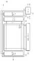
도 1은 본 발명의 실시예에 따른 표시장치의 분해 사시도이다.
도 2는 Ⅰ-Ⅰ'을 따라 절단한 도 1에 도시된 표시 장치의 단면도 이다.
도 3은 도 1에 도시된 표시 장치의 블록도 이다.
도 4는 도 3에 도시된 표시 패널의 일부를 확대한 평면도 이다.
도 5는 Ⅱ-Ⅱ'를 따라 절단한 도 4에 도시된 표시 패널의 단면도이다.
도 6은 Ⅲ-Ⅲ'을 따라 절단한 도 4에 도시된 표시 패널의 단면도 이다.
도 7은 본 발명의 다른 실시예에 따른 표시 패널의 평면도 이다.1 is an exploded perspective view of a display device according to an embodiment of the present invention.
2 is a cross-sectional view of the display device shown in Fig. 1 cut along the line I-I '.
3 is a block diagram of the display device shown in Fig.
4 is an enlarged plan view of a part of the display panel shown in Fig.
5 is a cross-sectional view of the display panel shown in Fig. 4 cut along II-II '.
6 is a cross-sectional view of the display panel shown in Fig. 4 cut along III-III '.
7 is a plan view of a display panel according to another embodiment of the present invention.
본 발명은 다양한 변경을 가할 수 있고 여러 가지 형태를 가질 수 있는 바, 특정 실시예들을 도면에 예시하고 본문에 상세하게 설명하고자 한다. 그러나, 이는 본 발명을 특정한 개시 형태에 대해 한정하려는 것이 아니며, 본 발명의 사상 및 기술 범위에 포함되는 모든 변경, 균등물 내지 대체물을 포함하는 것으로 이해되어야 한다.The present invention is capable of various modifications and various forms, and specific embodiments are illustrated in the drawings and described in detail in the text. It should be understood, however, that the invention is not intended to be limited to the particular forms disclosed, but includes all modifications, equivalents, and alternatives falling within the spirit and scope of the invention.
각 도면을 설명하면서 유사한 참조부호를 유사한 구성요소에 대해 사용하였다. 첨부된 도면에 있어서, 구조물들의 치수는 본 발명의 명확성을 위하여 실제보다 확대하여 도시한 것이다. 제1, 제2 등의 용어는 다양한 구성요소들을 설명하는데 사용될 수 있지만, 상기 구성요소들은 상기 용어들에 의해 한정되어서는 안 된다. 상기 용어들은 하나의 구성요소를 다른 구성요소로부터 구별하는 목적으로만 사용된다. 예를 들어, 본 발명의 권리 범위를 벗어나지 않으면서 제1 구성요소는 제2 구성요소로 명명될 수 있고, 유사하게 제2 구성요소도 제1 구성요소로 명명될 수 있다. 단수의 표현은 문맥상 명백하게 다르게 뜻하지 않는 한, 복수의 표현을 포함한다.Like reference numerals are used for like elements in describing each drawing. In the accompanying drawings, the dimensions of the structures are shown enlarged from the actual for the sake of clarity of the present invention. The terms first, second, etc. may be used to describe various components, but the components should not be limited by the terms. The terms are used only for the purpose of distinguishing one component from another. For example, without departing from the scope of the present invention, the first component may be referred to as a second component, and similarly, the second component may also be referred to as a first component. The singular expressions include plural expressions unless the context clearly dictates otherwise.
본 출원에서, "포함하다" 또는 "가지다" 등의 용어는 명세서 상에 기재된 특징, 숫자, 단계, 동작, 구성요소, 부품 또는 이들을 조합한 것이 존재함을 지정하려는 것이지, 하나 또는 그 이상의 다른 특징들이나 숫자, 단계, 동작, 구성요소, 부분품 또는 이들을 조합한 것들의 존재 또는 부가 가능성을 미리 배제하지 않는 것으로 이해되어야 한다. 또한, 층, 막, 영역, 판 등의 부분이 다른 부분 "위에" 있다고 할 경우, 이는 다른 부분 "바로 위에" 있는 경우뿐만 아니라 그 중간에 또 다른 부분이 있는 경우도 포함한다. 반대로 층, 막, 영역, 판 등의 부분이 다른 부분 "아래에" 있다고 할 경우, 이는 다른 부분 "바로 아래에" 있는 경우뿐만 아니라 그 중간에 또 다른 부분이 있는 경우도 포함한다.In the present application, the terms "comprises" or "having" and the like are used to specify that there is a feature, a number, a step, an operation, an element, a component or a combination thereof described in the specification, But do not preclude the presence or addition of one or more other features, integers, steps, operations, components, parts, or combinations thereof. Also, where a section such as a layer, a film, an area, a plate, or the like is referred to as being "on" another section, it includes not only the case where it is "directly on" another part but also the case where there is another part in between. On the contrary, where a section such as a layer, a film, an area, a plate, etc. is referred to as being "under" another section, this includes not only the case where the section is "directly underneath"
이하, 첨부한 도면들을 참조하여 본 발명의 바람직한 실시예를 보다 상세하게 설명하고자 한다.Hereinafter, preferred embodiments of the present invention will be described in detail with reference to the accompanying drawings.
도 1은 본 발명의 실시예에 따른 표시장치의 분해 사시도이며, 도 2는 Ⅰ-Ⅰ'을 따라 절단한 도 1에 도시된 표시 장치의 단면도 이다.FIG. 1 is an exploded perspective view of a display device according to an embodiment of the present invention, and FIG. 2 is a cross-sectional view of the display device shown in FIG. 1 cut along a line I-I '.
도 1 및 도 2를 참조하면, 본 발명의 일 실시예에 따른 표시장치(1000)는 표시 패널(100), 광학 부재(200), 도광판(300), 및 반사판(400)을 포함한다.1 and 2, a
상기 표시 패널(100)은 패널 광원부 및 표시부(120), 및 제1 기판(130)을 포함한다. 상기 표시 패널(100)은 예를 들어, 평행한 한 쌍의 단변들 및 평행한 한 쌍의 장변들을 포함하는 직사각형 형태를 가질 수 있다.The
상기 제1 기판(130)은 광원부 영역 및 표시부 영역(DA)을 포함한다. 상기 광원부 영역은 상기 제1 기판(130)의 좌측에 구비되는 제1 광원부 영역(LA1) 및 상기 제1 기판(130)의 우측에 구비되는 제2 광원부 영역(LA2)를 포함한다. 상기 표시부 영역(DA)은 상기 제1 및 제2 광원부 영역(LA1, LA2) 사이에 개재된다.The
상기 패널 광원부는 상기 제1 및 제2 광원부 영역(LA1, LA2)에 대응하여 상기 제1 기판(130)의 상면(131)에 각각 구비되는 제1 패널 광원부(110a) 및 제2 패널 광원부(110b)를 포함한다. 상기 제1 및 제2 패널 광원부(110a, 110b)는 제1 광(L1)을 생성한다. 보다 구체적으로, 상기 제1 및 제2 패널 광원부(110a, 110b) 각각은 상기 제1 광(L1)을 생성하고, 제2 방향(D2) 측으로 상기 제1 광(L1)을 방출한다. 상기 제1 광(L1)은 상기 제1 기판(130)을 통과하여 상기 도광판(300)에 제공된다.The panel light source unit includes a first panel
상기 도광판(300)은 상기 광학 부재(200)를 사이에 두고 상기 표시 패널(100)과 대향한다. 다시 말해 상기 도광판(300)은 상기 표시 패널(100)과 상기 제2 방향(D2)으로 인접하여 배치될 수 있다. 상기 도광판(300)은 상기 제2 방향(D2)과 수직한 수평 평면에서 상기 표시 패널(100)과 오버랩 될 수 있다.The
상기 도광판(300)은 상기 제1 및 제2 광원부 영역(LA1, LA2)에 대응하여 정의되는 입광부(310) 및 상기 표시부 영역(DA)에 대응하여 정의되는 출광부(320), 및 반사부재(330)를 포함한다.The
상기 출광부(320)는 상기 광학 부재(200)와 마주하는 출광면(321)을 포함한다. 상기 출광면(321)은 상기 표시부 영역(DA)에 대응하여 정의 될 수 있다. 또한, 상기 출광부(320)는 출광 패턴(322)를 포함한다. 상기 출광 패턴(322)은 예를 들어, 상기 출광부(320)의 하면(323)으로부터 상기 제2 방향(D2)과 반대하는 제1 방향(D1)으로 돌출된 돌기 형태를 가질 수 있다.The
상기 입광부(310)는 상기 표시 패널(100)을 마주하는 입광면(311)을 포함한다. 상기 입광면(311)은 상기 제1 및 제2 광원부 영역(LA1, LA2)에 대응하여 정의 될 수 있다.The light-
상기 반사 부재(330)는 상기 입광부(310)에 배치된다. 상기 반사 부재(330)는 수신한 광을 상기 출광부(320)측으로 반사 시킬 수 있도록 소정 각도 기울어져 있다. 보다 구체적으로, 상기 반사 부재(330)의 제1 면(331)과 평행한 면과 상기 입광면(311)이 이루는 각(θ)은 둔각 일 수 있다. 상기 반사 부재(330)는 광을 반사 시킬 수 있는 물질을 포함할 수 있다.The
상기 입광면(311)은 상기 제1 기판(130)을 통과하는 상기 제1 광(L1)을 수신한다. 상기 입광면(311)을 통과한 상기 제1 광(L1)은 상기 반사 부재(330)의 제1 면(331)에 의하여 상기 출광부(320) 측으로 제2 광(L2)으로써 반사된다. 상기 제2 광(L2)은 상기 입광부(310) 및 상기 출광부(320)에 의해 가이드 된 후, 상기 출광 패턴(322)에 의해 상기 광학 부재(200)측으로 출력 된다.The
상기 반사판(400)은 상기 도광판(300)의 상기 제2 방향(D2) 측에 배치되고, 상기 제1 광(L1) 및 상기 제2 광(L2) 중 상기 표시 패널(100) 방향으로 제공되지 않고 누설되는 광을 상기 표시 패널(100) 측으로 반사시킬 수 있다. 상기 반사판(400)은 예를 들어, 폴리에틸렌 테레프탈레이트(polyethylene terephthalate, PET) 및 알루미늄과 같은 광을 반사하는 물질을 포함한다.The
상기 광학 부재(200)는 상기 도광판(300) 및 상기 표시 패널(100) 사이에 개재된다. 상기 광학 부재(200)는 상기 수평 평면 상에서 상기 표시부 영역(DA)과 오버랩 된다.The
상기 광학 부재(200)는 예를 들어, 광을 확산하기 위한 한 장의 확산 시트(미도시) 및 광을 집광하기 위한 두 장의 집광 시트(미도시)를 포함할 수 있다.The
상기 확산 시트는 상기 도광판(300) 상에 배치되어 상기 도광판(300)으로부터 출사된 광을 확산시킨다. 상기 확산 시트는 투명한 물질, 예를 들어, 폴리에틸렌 테레프탈레이트(PET: Polyethylene Terephthalate) 재질로 형성될 수 있다.The diffusion sheet is disposed on the
상기 집광 시트들은 상기 확산 시트의 상부에 배치되고, 상기 확산 시트를 통해 확산된 광을 집광하여 정면 휘도를 향상시킨다. 상기 집광 시트들 각각은 프리즘 형상을 갖는 미세한 프리즘 패턴(미도시)을 구비할 수 있다. 특히, 상기 집광 시트들은 서로 다른 방향으로 연장된 프리즘 패턴들을 각각 포함할 수 있다.The light condensing sheets are disposed on the diffusion sheet, and light diffused through the diffusion sheet is condensed to improve the front luminance. Each of the light condensing sheets may have a fine prism pattern (not shown) having a prism shape. In particular, the light condensing sheets may each include prism patterns extending in different directions.
상기 광학 부재(200)가 상기 수평 평면 상에서 상기 제1 및 제2 광원부 영역(LA1, LA2)과 오버랩 되는 경우, 상기 입광면(311)으로 제공되는 상기 제1 광(L1)이 확산되고, 그 결과 상기 제1 광(L1)이 상기 입광면(311)에 효율적으로 제공될 수 없다.When the
따라서, 상기 광학 부재(200)는 상기 제1 광(L1)이 효율적으로 상기 입광면(311)에 도달 할 수 있도록, 상기 제1 및 제2 광원부 영역(LA1, LA2)과 상기 수평 평면 상에서 오버랩 되지 않을 수 있다.Therefore, the
상기 광학 부재(200)를 통과한 상기 제2 광(L2)은 상기 표시부 영역(DA)의 하면(132)에 도달한다.The second light L2 having passed through the
상기 표시부(120)는 상기 표시부 영역(DA)에 대응하여 상기 제1 기판(130)의 상기 상면(131)에 제공된다. 즉, 상기 표시부(120)는 상기 제1 및 제2 패널 광원부(110a, 110b) 사이에 개재된다. 상기 표시부(120)는 상기 표시부 영역(DA)의 하면(132)측으로 제공된 상기 제2 광(L2)을 수신 받고, 수신 받은 상기 제2 광(L2)을 이용하여 영상을 표시 한다.The
상술한 내용을 종합하면, 상기 제1 기판(130)에는 상기 제1 및 제2 패널 광원부(110a, 110b) 및 상기 표시부(120)가 배치되고, 상기 표시부(120)는 상기 제1 및 제2 패널 광원부(110a, 110b)로부터 제공된 광을 이용하므로, 상기 표시 장치(1000)는 상기 표시 패널(100)의 하측에 별도의 광원을 구비하기 위한 공간을 필요로 하지 않는다. 그 결과, 상기 표시 장치(1000)의 두께가 감소될 수 있다.The first and second
또한, 상기 표시 패널(100)에 상기 제1 및 제2 패널 광원부(110a, 110b)가 구비되므로, 별도의 광원을 조립할 필요가 없다. 그에 따라, 별도의 광원을 조립하는 경우 발생하는 조립 편차에 의한 화질의 불균일성이나, 별도의 광원 자체에서 비롯되는 화질의 불균일성이 발생되는 것을 방지 할 수 있다.In addition, since the
도 3은 도 1에 도시된 표시 장치의 블록도 이다.3 is a block diagram of the display device shown in Fig.
도 3을 참조하면, 상기 표시 장치(1000)는 상기 표시 패널(100)을 구동하는 게이트 구동부(500) 및 데이터 구동부(600), 상기 게이트 구동부(500)와 상기 데이터 구동부(600)의 구동을 제어하는 제어부(700)를 포함한다.3, the
상기 제어부(700)는 상기 표시 장치(1000)의 외부로부터 입력 영상(RGB) 및 복수의 제어신호(CS)를 수신한다. 상기 제어부(700)는 상기 데이터 구동부(600)의 인터페이스 및 상기 표시 패널(100)의 사양에 맞도록 상기 입력 영상(RGB)의 데이터 포맷을 변환하여 출력 영상 데이터(ID)를 생성하고, 상기 출력 영상 데이터(ID)를 상기 데이터 구동부(600)에 제공한다.The
또한, 상기 제어부(700)는 상기 복수의 제어신호(CS)에 근거하여 데이터 제어신호(DCS, 예를 들어, 출력개시신호, 수평개시신호 등) 및 게이트 제어신호(GCS, 예를 들어, 수직개시신호, 수직클럭신호, 및 수직클럭바신호)를 생성한다. 상기 데이터 제어신호(DCS)는 상기 데이터 구동부(600)로 제공되고, 상기 게이트 제어신호(GCS)는 상기 게이트 구동부(500)로 제공된다.The
상기 게이트 구동부(500)는 상기 제어부(700)로부터 제공되는 상기 게이트 제어신호(GCS)에 응답하여 게이트 신호들을 순차적으로 출력한다.The
상기 데이터 구동부(600)는 상기 제어부(700)로부터 제공되는 상기 데이터 제어신호(DCS)에 응답해서 상기 출력 영상 데이터(ID)를 데이터 전압들로 변환하여 상기 표시 패널(100)로 출력한다.The
상기 표시 패널(100)은 복수의 게이트 라인(GL1~GLn), 복수의 데이터 라인(DL1~DLm), 및 복수의 화소(PX)를 더 포함한다. The
상기 화소들(PX)은 영상을 구성하는 단위 영상을 표시하는 소자이다. 상기 표시 패널(100)에 구비된 상기 화소들(PX)의 개수에 따라 상기 표시 패널(100)의 해상도가 결정 될 수 있다. 도 3에서는 하나의 화소(PX)만을 도시하였으며 나머지 화소들에 대한 도시는 생략하였다.The pixels PX are elements for displaying a unit image constituting an image. The resolution of the
각 화소(PX)는 주요색(primary color)들 중 하나를 표시할 수 있다. 주요색들은 레드, 그린, 블루, 및 화이트를 포함할 수 있다. 그러나, 이에 한정되지 않고, 주요색들은 옐로우, 시안, 및 마젠타 등 다양한 색을 더 포함할 수 있다.Each pixel PX may represent one of the primary colors. The primary colors may include red, green, blue, and white. However, the present invention is not limited to this, and the main colors may further include various colors such as yellow, cyan, and magenta.
상기 복수의 게이트 라인(GL1~GLn)은 제3 방향(D3)으로 연장되고 상기 제3 방향(D3)과 수직한 제4 방향(D4)으로 서로 평행하게 배열된다. 상기 복수의 게이트 라인(GL1~GLn)은 상기 게이트 구동부(500)와 연결되어, 상기 게이트 구동부(500)로부터 상기 게이트 신호들을 순차적으로 수신한다.The plurality of gate lines GL1 to GLn extend in a third direction D3 and are arranged in parallel to each other in a fourth direction D4 perpendicular to the third direction D3. The plurality of gate lines GL1 to GLn are connected to the
상기 복수의 데이터 라인(DL1~DLm)은 상기 제4 방향(D4)으로 연장되고, 상기 제3 방향(D3)으로 서로 평행하게 배열된다. 상기 복수의 데이터 라인(DL1~DLm)은 상기 데이터 구동부(600)와 연결되어 상기 데이터 구동부(600)로부터 상기 데이터 전압들을 수신한다.The plurality of data lines DL1 to DLm extend in the fourth direction D4 and are arranged in parallel to each other in the third direction D3. The plurality of data lines DL1 to DLm are connected to the
상기 화소들(PX)은 상기 게이트 라인들(GL1~GLn) 중 대응하는 게이트 라인 및 상기 데이터 라인들(DL1~DLm) 중 대응하는 데이터 라인과 연결되어 구동 될 수 있다. 보다 구체적으로, 상기 화소들(PX)은 상기 게이트 신호에 의해 제어되고, 상기 데이터 전압에 대응되는 영상을 표시한다.The pixels PX may be driven by being connected to corresponding gate lines among the gate lines GL1 to GLn and corresponding data lines among the data lines DL1 to DLm. More specifically, the pixels PX are controlled by the gate signal and display an image corresponding to the data voltage.
상기 제어부(700)는 상기 제1 및 제2 패널 광원부(110a, 110b)을 제어하기 위한 광원 제어 신호(LCS)를 생성한다. 상기 제1 및 제2 패널 광원부(110a, 110b)는 상기 광원 제어 신호(LCS)에 응답 하여 상기 제1 광(L1, 도 2에 도시됨)을 생성한다. 보다 구체적으로, 상기 제1 광(L1)의 휘도, 컬러, 및 상기 제1 광(L1)이 생성되는 타이밍은 상기 광원 제어 신호(LCS)에 의해 제어될 수 있다.The
상기 제어부(700)는 집적 회로 칩의 형태로 인쇄 회로 기판(미도시)상에 실장되어 상기 게이트 구동부(500) 및 상기 데이터 구동부(600)에 연결될 수 있다. 상기 게이트 구동부(500) 및 상기 데이터 구동부(600)는 복수의 구동 칩들로 형성되어 연성 인쇄 회로(FPC: Flexible Printed Circuit, 미도시) 기판상에 실장되고, 테이프 캐리어 패키지(TCP: Tape Carrier Package) 방식으로 상기 표시 패널(100)에 연결될 수 있다.The
그러나, 이에 한정되지 않고, 상기 게이트 구동부(500) 및 상기 데이터 구동부(600)는 복수의 구동 칩들로 형성되어 상기 표시 패널(100)에 칩 온 글래스(COG: Chip on Gass) 방식으로 실장될 수 있다. 또한, 상기 게이트 구동부(500)는 상기 화소들(PX)과 함께 동시에 형성되어 ASG(Amorphous Silicon TFT Gate driver circuit) 형태로 상기 표시 패널(100)에 실장될 수 있다.However, the present invention is not limited thereto. The
본 발명의 일 예에 따른 상기 게이트 구동부(500)는 상기 표시 패널(100)에 ASG 형태로 실장되며, 상기 데이터 구동부(600)는 상기 연성 인쇄 회로에 형성되는 구동 칩들에 의해 구현 된다.The
도 4는 도 3에 도시된 표시 패널의 일부를 확대한 평면도 이다.4 is an enlarged plan view of a part of the display panel shown in Fig.
도 3 및 도 4를 참조하면, 상기 표시 패널(100)은 광원 제어 라인(LCL) 및 게이트 제어 라인(GCL)을 포함한다. 도 4에서는 상기 제1 내지 제m 데이터 라인(DL1~DLm) 중 제1 및 제2 데이터 라인(DL1, DL2) 만을 도시 하였으며, 상기 제1 내지 제n 게이트 라인(GL1~GLn) 중 제1 및 제2 게이트 라인(GL1, GL2) 만을 도시 하였다.3 and 4, the
한편, 상기 표시 패널(100)의 상기 표시부 영역(DA)은 게이트 구동부 영역(GA) 및 매트릭스 영역(MA)을 포함한다. 상기 게이트 구동부 영역(GA)은 상기 매트릭스 영역(MA) 및 상기 제1 광원부 영역(LA1) 사이에 개재될 수 있다.Meanwhile, the display area DA of the
상기 매트릭스 영역(MA)의 상기 제4 방향(D4) 측에는 패드 영역(PA)이 정의 될 수 있다. 상기 패드 영역(PA)은 상기 연성 인쇄 회로와 오버랩되는 영역이다. 상기 연성 인쇄 회로는 상기 제어부(700)로부터 생성되는 상기 광원 제어 신호(LCS), 상기 게이트 제어 신호(GCS), 및 상기 데이터 구동부(600)에서 생성되는 상기 데이터 전압들을 상기 표시 패널(100)에 전달 해준다.A pad region PA may be defined in the fourth direction D4 of the matrix region MA. The pad area PA is an area overlapping with the flexible printed circuit. The flexible printed circuit includes the
상기 광원 제어 라인(LCL)은 상기 제1 기판(130)의 상기 상면(131)에 제공된다. 보다 구체적으로, 상기 광원 제어 라인(LCL)의 일단은 상기 패드 영역(PA)에 구비되고, 상기 연성 인쇄 회로와 전기적으로 연결될 수 있다. 상기 광원 제어 라인(LCL)의 타단은 상기 제1 패널 광원부(110a)와 연결된다. 상기 광원 제어 라인(LCL)은 상기 제어부(700)로부터 생성되는 광원 제어 신호(LCS)를 상기 제1 패널 광원부(110a)에 전달한다.The light source control line LCL is provided on the
상기 게이트 구동부 영역(GA)에는 게이트 구동부(500)가 구비된다. 상기 게이트 구동부(500)는 상기 매트릭스 영역(MA)에 형성되는 화소(PX)의 트랜지스터(TR)와 함께 동시에 ASG 형태로 실장 될 수 있다.A
상기 게이트 제어 라인(GCL)은 상기 제1 기판(130)의 상기 상면(131)에 배치된다. 보다 구체적으로, 상기 게이트 제어 라인(GCL)의 일단은 상기 패드 영역(PA)에 구비되고, 상기 연성 인쇄 회로와 전기적으로 연결 될 수 있다. 상기 게이트 제어 라인(GCL)의 타단은 상기 게이트 구동부(500)와 연결될 수 있다. 상기 게이트 제어 라인(GCL)은 상기 제어부(700)로부터 생성되는 상기 게이트 제어 신호(GCS)를 상기 게이트 구동부(500)에 전달해 준다.The gate control line GCL is disposed on the
상기 매트릭스 영역(MA)에는 상기 화소들(PX)이 매트릭스 형태로 배치된다. 도 3에서는 간단한 설명을 위해 하나의 화소(PX)만을 예시적으로 도시하였다. 상기 화소(PX)는 상기 게이트 라인들 및 상기 데이터 라인들에 의해서 정의되는 화소 영역(PA) 마다 구비될 수 있다.The pixels PX are arranged in a matrix form in the matrix region MA. In FIG. 3, only one pixel PX is exemplarily shown for the sake of simplicity. The pixel PX may be provided for each pixel region PA defined by the gate lines and the data lines.
상기 제1 및 제2 게이트 라인(GL1, GL2)은 상기 제1 기판(130)의 상기 상면(131) 상에 배치된다. 상기 제1 및 제2 게이트 라인(GL1, GL2)의 일단은 상기 게이트 구동부(500)와 연결되고, 상기 게이트 구동부(500)에서 생성된 상기 게이트 신호를 상기 화소(PX)에 전달한다.The first and second gate lines GL1 and GL2 are disposed on the
상기 제1 및 제2 데이터 라인(DL1, DL2)은 상기 제1 기판(130)의 상기 상면(131) 상에 상기 게이트 라인과 절연되어 배치된다. 상기 제1 및 제2 데이터 라인(DL1, DL2)의 일단은 상기 패드 영역(PA)에 배치되고, 상기 연성 인쇄 회로와 전기적으로 연결된다. 상기 제1 및 제2 데이터 라인(DL1, DL2)은 상기 데이터 구동부(600)에서 생성된 상기 데이터 전압을 상기 화소(PX)에 전달 한다.The first and second data lines DL1 and DL2 are disposed on the
본 발명의 일 예로, 상기 광원 제어 라인(LCL)은 상기 게이트 제어 라인(GCL)과 동일한 층에 배치 될 수 있다. 이 경우, 상기 광원 제어 라인(LCL)은 상기 게이트 제어 라인(GCL)과 동일한 공정을 통해 형성 될 수 있다.In an embodiment of the present invention, the light source control line (LCL) may be disposed on the same layer as the gate control line (GCL). In this case, the light source control line LCL may be formed through the same process as the gate control line GCL.
또한 이에 한정되지 않고, 상기 광원 제어 라인(LCL)은 상기 게이트 라인 및 상기 데이터 라인 중 어느 하나와 동일한 층에 형성 될 수 있다. 이 경우 상기 광원 제어 라인(LCL)은 상기 게이트 라인 및 상기 데이터 라인 중 어느 하나와 동일한 공정을 통해 형성 될 수 있다.The light source control line (LCL) may be formed on the same layer as any one of the gate line and the data line. In this case, the light source control line (LCL) may be formed through the same process as any one of the gate line and the data line.
이와 같이, 상기 광원 제어 라인(LCL)은 상기 제1 기판(130)의 상기 상면(131)에 배선을 형성 하여 구현할 수 있으므로, 상기 패널 광원과 연결되기 위한 별도의 배선이 요구 하지 않는다. 그 결과, 상기 표시 장치(1000)의 구조가 간단해지고, 그에 따라 상기 표시 장치(1000)를 제조하기 위한 비용이 절감될 수 있다. 더욱이, 상기 광원 제어 라인(LCL)은 상기 제1 기판(130)의 상기 상면(131) 상에 형성되는 다른 라인과 함께 형성 될 수 있으므로, 간단하게 형성 될 수 있다.Since the light source control line LCL can be formed by forming the wiring on the
도 5는 Ⅱ-Ⅱ'를 따라 절단한 도 4에 도시된 표시 패널의 단면도이다.5 is a cross-sectional view of the display panel shown in Fig. 4 cut along II-II '.
도 5를 참조하면, 상기 제1 패널 광원부(110a)는 발광 소자(OE)를 포함한다. 본 발명의 일 예로, 상기 발광 소자(OE)는 유기 발광 소자를 포함할 수 있다. 그러나 이에 한정되지 않고, 상기 발광 소자(OE)는 GaAs(Gallium arsenide)와 같은 무기물로 구성되는 발광 다이오드 (LED: Light Emitting Diode)를 포함할 수 있다.Referring to FIG. 5, the first panel
상기 발광 소자(OE)는 제1 전극(E1), 제1 캐리어 수송 영역(CTR1), 발광층(EML), 제2 캐리어 수송 영역(CTR2), 및 제2 전극(E2)를 포함한다. 상기 제1 전극(E1)은 상기 제1 기판(130)의 상기 상면(131)에 구비되고, 상기 제1 전극(E1) 상에 상기 발광층(EML) 상기 제2 전극(E2)이 순차적으로 적층된다. 상기 제2 전극(E2)은 상기 발광층(EML)을 사이에 두고 상기 제1 전극(E1)과 대향 한다.The light emitting device OE includes a first electrode E1, a first carrier transport region CTR1, a light emitting layer EML, a second carrier transport region CTR2, and a second electrode E2. The first electrode E1 is provided on the
상기 제1 전극(E1)은 투명 전극 일 수 있다. 이 경우 상기 제1 전극(E1)은 투명 금속 산화물, 예를 들어, ITO(indium tin oxide), IZO(indium zinc oxide), ZnO(zinc oxide), ITZO(indium tin zinc oxide)를 포함할 수 있다. 본 발명의 일 예로, 상기 제1 전극(E1)은 정공을 제공하는 애노드 일 수 있다. 그러나 이에 한정되지 않고 상기 제1 전극(E1)은 전자를 제공하는 캐소드일 수 있다.The first electrode E1 may be a transparent electrode. In this case, the first electrode E1 may include a transparent metal oxide, for example, ITO (indium tin oxide), IZO (indium zinc oxide), ZnO (zinc oxide), ITZO (indium tin zinc oxide) . In one embodiment of the present invention, the first electrode E1 may be an anode providing holes. However, the first electrode E1 may be a cathode that provides electrons.
상기 제2 전극(E2)은 반투과 전극 또는 반사 전극 일 수 있다. 이 경우 상기 제2 전극(E2)은 Ag, Mg, Al, Pt, Pd, Au, Ni, Nd, Ir, Cr, Li, Ca, LiF/Ca, LiF/Al, Mo, Ti 또는 이들의 화합물이나 혼합물(예를 들어, Ag와 Mg의 혼합물)을 포함할 수 있다. 본 발명의 일 예로, 상기 제2 전극(E2)은 캐소드이다. 그러나 이에 한정되지 않고 상기 제2 전극은 애노드 일 수도 있다.The second electrode E2 may be a transflective electrode or a reflective electrode. In this case, the second electrode E2 may be formed of Ag, Mg, Al, Pt, Pd, Au, Ni, Nd, Ir, Cr, Li, Ca, LiF / Ca, LiF / (E. G., A mixture of Ag and Mg). In an example of the present invention, the second electrode E2 is a cathode. However, the second electrode may be an anode.
상기 발광층(EML)은 단일 물질로 이루어진 단일층, 복수의 서로 다른 물질로 이루어진 단일층 또는 복수의 서로 다른 물질로 이루어진 복수의 층을 갖는 다층 구조를 가질 수 있다.The light emitting layer (EML) may have a single layer made of a single material, a single layer made of a plurality of different materials, or a multi-layered structure having a plurality of layers made of a plurality of different materials.
상기 발광층(EML)은 진공 증착법, 스핀 코팅법, 캐스트법, LB법(Langmuir-Blodgett), 잉크젯 프린팅법, 레이저 프린팅법, 레이저 열전사법(Laser Induced Thermal Imaging, LITI) 등과 같은 다양한 방법을 이용하여 형성될 수 있다.The light emitting layer (EML) may be formed using various methods such as vacuum deposition, spin coating, casting, LB method, inkjet printing, laser printing, .
상기 발광층(EML)은 통상적으로 사용하는 유기 발광 물질이라면 특별히 한정되지 않으나, 예를 들어, 적색, 녹색 및 청색을 발광하는 물질로 이루어질 수 있으며, 형광물질 또는 인광물질을 포함할 수 있다. 또한, 상기 발광층(EML)은 호스트 및 도펀트를 포함할 수 있다.The light emitting layer (EML) is not particularly limited as long as it is a commonly used organic light emitting material. For example, the light emitting layer (EML) may comprise a material emitting red, green, and blue light and may include a fluorescent material or a phosphorescent material. The light emitting layer (EML) may include a host and a dopant.
상기 호스트는 통상적으로 사용하는 물질이라면 특별히 한정하지 않으나, 예를 들어, Alq3(tris(8-hydroxyquinolino)aluminum), CBP(4,4'-bis(N-carbazolyl)-1,1'-biphenyl), PVK(poly(n-vinylcabazole)), ADN(9,10-di(naphthalene-2-yl)anthracene), TCTA(4,4',4''-Tris(carbazol-9-yl)-triphenylamine), TPBi(1,3,5-tris(N-phenylbenzimidazole-2-yl)benzene), TBADN(3-tert-butyl-9,10-di(naphth-2-yl)anthracene), DSA(distyrylarylene), CDBP(4,4′-bis(9-carbazolyl)-2,2′-dimethyl-biphenyl), MADN(2-Methyl-9,10-bis(naphthalen-2-yl)anthracene) 등을 사용될 수 있다.For example, Alq3 (tris (8-hydroxyquinolino) aluminum), CBP (4,4'-bis (N-carbazolyl) -1,1'-biphenyl) , PVK (n-vinylcabazole), ADN (naphthalene-2-yl) anthracene, TCTA (4,4 ', 4 "-tris (carbazol- , TPBi (1,3,5-tris (N-phenylbenzimidazole-2-yl) benzene), TBADN (3-tert-butyl-9,10- di (naphth- (9-carbazolyl) -2,2'-dimethyl-biphenyl, MADN (2-Methyl-9,10-bis (naphthalen-2-yl) anthracene).
상기 발광층(EML)이 적색을 발광할 때, 상기 발광층(EML)은 예를 들어, PBD:Eu(DBM)3(Phen)(tris(dibenzoylmethanato)phenanthoroline europium) 또는 퍼릴렌(Perylene)을 포함하는 형광물질을 포함할 수 있다. 상기 발광층(EML)이 적색을 발광할 때, 상기 발광층(EML)에 포함되는 도펀트는 예를 들어, PIQIr(acac)(bis(1-phenylisoquinoline)acetylacetonate iridium), PQIr(acac)(bis(1-phenylquinoline)acetylacetonate iridium), PQIr(tris(1-phenylquinoline)iridium) 및 PtOEP(octaethylporphyrin platinum)과 같은 금속 착화합물(metal complex) 또는 유기 금속 착체(organometallic complex)에서 선택할 수 있다.When the light emitting layer (EML) emits red light, the light emitting layer (EML) may include, for example, a fluorescent material containing PBD: Eu (DBM) 3 (Phen) (tris (dibenzoylmethanato) phenanthoroline europium) or perylene ≪ / RTI > When the light emitting layer EML emits red light, the dopant included in the light emitting layer EML includes, for example, bis (1-phenylisoquinoline) acetylacetonate iridium, PQIr (acac) bis (1- a metal complex or an organometallic complex such as phenylquinoline acetylacetonate iridium, PQIr (tris (1-phenylquinoline) iridium) and PtOEP (octaethylporphyrin platinum).
상기 발광층(EML)이 녹색을 발광할 때, 상기 발광층(EML)은 예를 들어, Alq3(tris(8-hydroxyquinolino)aluminum)을 포함하는 형광물질을 포함할 수 있다. 상기 발광층(EML)이 녹색을 발광할 때, 상기 발광층(EML)에 포함되는 도펀트는 예를 들어, Ir(ppy)3(fac-tris(2-phenylpyridine)iridium)와 같은 금속 착화합물(metal complex) 또는 유기 금속 착체(organometallic complex)에서 선택할 수 있다.When the light emitting layer EML emits green light, the light emitting layer EML may include a fluorescent material including, for example, Alq3 (tris (8-hydroxyquinolino) aluminum). When the light emitting layer EML emits green light, the dopant included in the light emitting layer EML may be a metal complex such as Ir (ppy) 3 (fac-tris (2-phenylpyridine) iridium) Or an organometallic complex.
상기 발광층(EML)이 청색을 발광할 때, 상기 발광층(EML)은 예를 들어, 스피로-DPVBi(spiro-DPVBi), 스피로-6P(spiro-6P), DSB(distyryl-benzene), DSA(distyryl-arylene), PFO(Polyfluorene)계 고분자 및 PPV(poly(p-phenylene vinylene)계 고분자로 이루어진 군에서 선택된 어느 하나를 포함하는 형광물질을 포함할 수 있다. 상기 발광층(EML)이 청색을 발광할 때, 상기 발광층(EML)에 포함되는 도펀트는 예를 들어, (4,6-F2ppy)2Irpic와 같은 금속 착화합물(metal complex) 또는 유기 금속 착체(organometallic complex)에서 선택할 수 있다.When the light emitting layer (EML) emits blue light, the light emitting layer (EML) may include, for example, spiro-DPVBi, spiro-6P, distyryl-benzene, DSA The light emitting layer EML may emit blue light. The light emitting layer EML may emit blue light. The light emitting layer EML may emit blue light. The dopant included in the light emitting layer (EML) can be selected from a metal complex or an organometallic complex such as (4,6-F2ppy) 2Irpic.
본 발명의 일 예로, 상기 제1 캐리어 수송 영역(CTR1)은 정공 수송 영역 일 수 있다. 상기 정공 수송 영역은, 정공 주입층, 정공 수송층, 버퍼층 및 전자 저지층 중 적어도 하나를 포함할 수 있다.In an exemplary embodiment of the present invention, the first carrier transport region CTR1 may be a hole transport region. The hole transporting region may include at least one of a hole injecting layer, a hole transporting layer, a buffer layer, and an electron blocking layer.
상기 정공 수송 영역은 단일 물질로 이루어진 단일층, 복수의 서로 다른 물질로 이루어진 단일층 또는 복수의 서로 다른 물질로 이루어진 복수의 층을 갖는 다층 구조를 가질 수 있다.The hole transporting region may have a single layer made of a single material, a single layer made of a plurality of different materials, or a multi-layered structure having a plurality of layers made of a plurality of different materials.
예를 들어, 상기 정공 수송 영역은, 복수의 서로 다른 물질로 이루어진 단일층의 구조를 갖거나, 상기 제1 전극(E1)으로부터 차례로 적층된 상기 정공 주입층/ 상기 정공 수송층, 상기 정공 주입층/ 상기 정공 수송층/ 상기 버퍼층의 구조를 가질 수 있으나, 이에 한정되는 것은 아니다.For example, the hole transporting region may have a structure of a single layer made of a plurality of different materials, or may have a structure in which the hole injecting layer / the hole transporting layer, the hole injecting layer / The structure of the hole transport layer / the buffer layer may be used, but the present invention is not limited thereto.
상기 제2 캐리어 수송 영역(CTR2)은 예를 들어 전자 수송 영역 일 수 있다. 상기 전자 수송 영역은, 정공 저지층, 전자 수송층 및 전자 주입층 중 적어도 하나를 포함할 수 있으나, 이에 한정되는 것은 아니다.The second carrier transport region CTR2 may be, for example, an electron transport region. The electron transport region may include at least one of a hole blocking layer, an electron transport layer, and an electron injection layer, but is not limited thereto.
예를 들어, 상기 전자 수송 영역은, 상기 발광층(EML)으로부터 차례로 적층된 전자 수송층/ 전자 주입층 또는 전자 수송층/ 전자 주입층/정공 저지층의 구조를 가지거나, 둘 이상의 층이 혼합된 단일층 구조를 가질 수 있으나, 이에 한정되는 것은 아니다.For example, the electron transporting region may have a structure of an electron transporting layer / electron injecting layer or an electron transporting layer / electron injecting layer / hole blocking layer sequentially stacked from the light emitting layer (EML) Structure, but is not limited thereto.
상기 표시 패널(100)은 제2 기판(140)을 더 포함한다. 상기 제2 기판(120)은 상기 발광 소자(OE)를 사이에 두고 상기 제1 기판(130)과 대향한다. 도 5에서는 도시되지 않았으나, 상기 표시 패널(100)은 상기 발광 소자(OE)를 봉지(encapsulate) 할 수 있는 실링 부재를 포함한다. 상기 실링 부재는 상기 제1 및 제2 기판(130, 140) 사이에 상기 발광 소자(OE)를 둘러 싸도록 제공되어, 상기 발광 소자(OE)를 외부의 습기 및 산소로부터 보호한다.The
또한, 본 발명의 다른 일 예로, 상기 발광 소자(OE)는 상기 발광 소자(OE)를 커버함으로써, 상기 발광 소자(OE)를 외부의 습기 및 산소로부터 보호하는 박막 봉지(TFE: Thin Film Encapsulation)에 의해 봉지 될 수 있다. 상기 박막 봉지는 단일 물질로 이루어진 단일막, 복수의 서로 다른 물질로 이루어진 단일막 또는 복수의 서로 다른 물질로 이루어진 복수의 막을 갖는 다층 막구조를 가질 수 있다. 상기 박막 봉지는 유기물, 무기물, 또는 이들의 조합으로 이루어진 물질을 포함할 수 있다.According to another embodiment of the present invention, the light emitting device OE may be a thin film encapsulation (TFE) device that protects the light emitting device OE from external moisture and oxygen by covering the light emitting device OE. As shown in Fig. The thin film encapsulation may have a multilayer film structure having a single film made of a single material, a single film made of a plurality of different materials, or a plurality of films made of a plurality of different materials. The thin film encapsulation may comprise a material comprising an organic material, an inorganic material, or a combination thereof.
상기 제1 및 제2 전극(E1, E2)에 구동 전압이 인가되어 상기 발광층(EML)에 구동 전류가 흐르는 경우. 상기 발광층(EML)은 상기 제1 광(L1)을 생성한다. 상기 제1 광(L1)은 바로 상기 제1 전극(E1) 및 상기 제1 기판(130)을 통해 상기 제2 방향(D2) 측으로 출력 되거나, 상기 제2 전극(E2)에 의해 반사되어 상기 제1 전극(E1) 및 상기 제1 기판(130)을 통해 상기 제2 방향(D2) 측으로 출력 된다.When a driving voltage is applied to the first and second electrodes E1 and E2 and a driving current flows in the light emitting layer (EML). The light emitting layer (EML) generates the first light L1. The first light L1 may be output to the second direction D2 through the first electrode E1 and the
전술한 바와 같이 상기 광원 제어 라인(LCL)은 상기 제1 기판(130)의 상기 상면(131) 상에 배치된다. 본 발명의 일 예로, 상기 제1 전극(E1)은 상기 광원 제어 라인(LCL)과 동일한 층에 형성 될 수 있다.The light source control line LCL is disposed on the
도 6은 Ⅲ-Ⅲ'을 따라 절단한 도 4에 도시된 표시 패널의 단면도 이다.6 is a cross-sectional view of the display panel shown in Fig. 4 cut along III-III '.
상기 표시부(120)는 하판(LS), 액정층(LC) 및 상판(US)을 포함한다.The
상기 하판(LS)은 상기 제1 기판(130), 제1 절연막(IL1), 제2 절연막(IL2), 제3 전극(E3), 및 트랜지스터(TR)을 포함한다.The lower substrate LS includes the
상기 트랜지스터(TR)는 게이트 전극(GE), 제1 절연막(IL1), 반도체층(AL) 소스 전극(SE), 및 드레인 전극(DE)을 포함한다. 상기 게이트 전극(GE)은 상기 제1 기판(130)상에 배치되며, 상기 제1 게이트 라인(GL1, 도 4에 도시됨)으로부터 분기된다. 상기 반도체층(AL)은 상기 제1 절연막(IL1)을 사이에 두고 상기 게이트 전극(GE) 위에 배치될 수 있다. 상기 소스 전극(SE)은 상기 제1 데이터 라인(DL1, 도 4에 도시됨)으로부터 분기되어 상기 반도체층(AL)과 접촉되고, 상기 드레인 전극(DE)은 상기 소스 전극(SE)과 이격되어 상기 반도체층(AL)과 접촉된다.The transistor TR includes a gate electrode GE, a first insulating film IL1, a semiconductor layer AL source electrode SE, and a drain electrode DE. The gate electrode GE is disposed on the
상기 제2 절연막(IL2)은 상기 트랜지스터(TR) 및 상기 제1 절연막(IL1)을 커버한다. 상기 제2 절연막(IL2)은 상기 제2 방향(D2) 측으로 함몰된 컨택홀(CNT)을 포함한다. 상기 컨택홀(CNT)에 의해 상기 드레인 전극(DE)의 상면이 노출 된다.The second insulating layer IL2 covers the transistor TR and the first insulating layer IL1. The second insulating layer IL2 includes a contact hole CNT that is recessed toward the second direction D2. And the upper surface of the drain electrode DE is exposed by the contact hole CNT.
상기 제3 전극(E3)은 상기 제2 절연막(IL2) 상에 배치되며, 상기 컨택홀(CNT)을 통해 노출된 상기 드레인 전극(DE)의 상면과 전기적으로 연결된다. 상기 제3 전극(E3)은 투명 금속 산화물, 예를 들어, ITO(indium tin oxide), IZO(indium zinc oxide), ITZO(indium tin zinc oxide) 등을 포함할 수 있다.The third electrode E3 is disposed on the second insulating layer IL2 and is electrically connected to the upper surface of the drain electrode DE exposed through the contact hole CNT. The third electrode E3 may include a transparent metal oxide, for example, indium tin oxide (ITO), indium zinc oxide (IZO), indium tin zinc oxide (ITZO), or the like.
상기 상판(US)은 상기 제2 기판(140), 컬러 필터(CF), 블랙 매트릭스(BM), 제4 전극(PE4)을 포함한다.The upper plate US includes the
상기 블랙 매트릭스(BM)는 차광 영역(미도시)에 대응하여 상기 제2 기판(140) 상에 형성된다. 상기 차광 영역은 상기 복수의 데이터 라인들, 상기 트랜지스터(TR) 및 상기 복수의 게이트 라인들에 대응되는 영역으로 정의될 수 있다. 상기 차광 영역에는 빛샘이 발생할 수 있다. 상기 블랙 매트릭스(BM)는 상기 차광 영역에 대응하여 형성되어 상기 빛샘을 차단한다.The black matrix BM is formed on the
상기 컬러 필터(CF)는 상기 제2 기판(140) 상에 형성되며, 상기 액정층(LC)을 투과하는 광의 특정한 파장에 대응하는 성분을 필터링 하여 색을 구현한다. 본 발명의 일 예로, 상기 컬러 필터(CF)가 상기 상판(US)에 제공된 것을 개시하였으나 이에 한정되는 것은 아니며, 상기 컬러 필터(CF)은 상기 하판(LS)에 제공될 수 있다.The color filter CF is formed on the
상기 제4 전극(E4)은 상기 컬러 필터(CF) 상에 형성된다. 상기 제4 전극(PE4)은 투명 도전성 물질로 형성될 수 있다. 상기 제4 전극(E4)은 투명 금속 산화물, 예를 들어, ITO(indium tin oxide), IZO(indium zinc oxide), ITZO(indium tin zinc oxide) 등을 포함할 수 있다.The fourth electrode E4 is formed on the color filter CF. The fourth electrode PE4 may be formed of a transparent conductive material. The fourth electrode E4 may include a transparent metal oxide, for example, indium tin oxide (ITO), indium zinc oxide (IZO), indium tin zinc oxide (ITZO), or the like.
상기 액정층(LC)은 상기 하판(LS) 및 상기 상판(US) 사이에 개재되며, 유전율 이방성 및 광학적 이방성을 갖는 액정 분자를 포함한다.The liquid crystal layer LC includes liquid crystal molecules interposed between the lower plate LS and the upper plate US and having dielectric anisotropy and optical anisotropy.
상기 화소(PX)는 상기 트랜지스터(TR), 상기 제3 전극(E3), 액정층(LC), 상기 제4 전극(E4), 상기 컬러 필터(CF)로 구성 될 수 있다. 상기 제2 광(L2)은 상기 제1 기판(130)을 통해 상기 화소(PX)로 공급 되고, 상기 제2 광(L2)은 상기 제3 및 제4 전극(E3, E4) 사이에 형성되는 전계에 따라 구동되는 상기 액정 분자에 의해 제어 된다.The pixel PX may be formed of the transistor TR, the third electrode E3, the liquid crystal layer LC, the fourth electrode E4, and the color filter CF. The second light L2 is supplied to the pixel PX through the
도 7은 본 발명의 다른 실시예에 따른 표시 패널의 평면도 이다.7 is a plan view of a display panel according to another embodiment of the present invention.
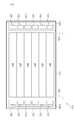
도 3및 도 7을 참조하면, 상기 제1 및 제2 패널 광원부(150a, 150b) 각각은 제1 내지 제6 서브 패널 광원부(151~156)를 포함할 수 있다.Referring to FIGS. 3 and 7, the first and second
상기 제1 내지 제6 서브 패널 광원부(151~156)는 상기 제4 방향(D4)을 따라 배열되어 하나의 열을 이룬다. 상기 제1 내지 제6 서브 패널 광원부(151~156)는 상기 광원 제어 라인(LCL)과 전기적으로 연결된다. 상기 제1 내지 제6 서브 패널 광원부(151~156)는 상기 광원 제어 라인(LCL)을 통해 제공되는 제1 내지 제6 서브 광원 제어 신호를 수신 받는다. 상기 제1 내지 제6 서브 패널 광원부(151~156)는 상기 제1 내지 제6 서브 광원 제어 신호에 각각 응답하여 독립적으로 구동 될 수 있다.The first to sixth sub-panel
본 발명의 일 예로, 상기 제어부(700)는 상기 입력 영상(RGB)를 분석하고, 분석한 결과를 근거로 상기 제1 내지 제6 서브 광원 제어 신호을 생성하여, 로컬 디밍 방식으로 제1 내지 제6 서브 패널 광원부(151~156)를 구동 할 수 있다.The
보다 구체적으로, 상기 제어부(700)는 상기 제1 내지 제6 서브 패널 광원부(151~156)들에 대응하여 상기 표시부(120)을 제1 내지 제6 영역(AR1~AR6)으로 구분하고, 상기 제1 내지 제6 영역(AR1~AR6)에 대응하는 상기 입력 영상(RGB)를 분석하여, 상기 제1 내지 제6 서브 광원 제어 신호를 생성한다.More specifically, the
예를 들어, 상기 제1 영역(AR1)에 대응되는 상기 입력 영상(RGB)의 평균적인 계조값은 크고, 상기 제6 영역(AR6)에 대응되는 상기 입력 영상(RGB)의 평균적인 계조값은 작은 경우, 상기 제1 서브 패널 광원부(151)에서 생성되는 광의 휘도가 상기 제6 서브 패널 광원부(156)에서 생성되는 광의 휘도 보다 크도록 상기 제1 및 제6 서브 광원 제어 신호을 생성할 수 있다.For example, the average gray-scale value of the input image RGB corresponding to the first area AR1 is large and the average gray-scale value of the input image RGB corresponding to the sixth area AR6 is large The first and sixth sub light source control signals may be generated such that the brightness of the light generated by the first sub-panel
본 발명의 일 예로, 상기 제1 내지 제6 서브 패널 광원부(151~156) 각각은 백색광을 생성할 수 있다. 이 경우, 상기 제1 내지 제6 서브 패널 광원부(151~156)의 상기 발광층(EML, 도 5에 도시됨)은 백색광을 생성하는 유기 발광 물질을 포함할 수 있다.In an example of the present invention, each of the first to sixth sub-panel
또한, 이에 한정되지 않고, 상기 제1 내지 제6 서브 패널 광원부(151~156) 각각은 서로 다른 컬러광을 생성하는 복수의 컬러 패널 광원부(미도시)를 포함할 수 있다. 본 발명의 일 예로, 상기 제1 내지 제6 서브 패널 광원부(151~156) 각각은 레드, 그린, 및 블루 컬러광을 생성하는 레드, 그린, 및 블루 패널 광원부를 포함할 수 있다. 이 경우, 상기 레드, 그린, 및 블루 패널 광원부의 발광층(EML)은 각각 레드, 그린, 및 블루광을 생성하는 유기 발광 물질을 포함할 수 있다. 이와 같이, 상기 제1 내지 제6 서브 패널 광원부(151~156)가 상기 컬러 패널 광원부들을 포함하는 경우, 상기 표시 패널(100)은 컬러 디밍 방식으로 구동 될 수 있다.The first to sixth sub-panel
이상 실시예를 참조하여 설명하였지만, 해당 기술 분야의 숙련된 당업자는 하기의 특허 청구의 범위에 기재된 본 발명의 사상 및 영역으로부터 벗어나지 않는 범위 내에서 본 발명을 다양하게 수정 및 변경시킬 수 있음을 이해할 수 있을 것이다.It will be understood by those skilled in the art that various changes in form and details may be made therein without departing from the spirit and scope of the invention as defined in the appended claims. It will be possible.
100: 표시 패널200: 광학 부재
300: 도광판400: 반사판
120: 표시부OE: 발광 소자
110a, 110b: 제1 및 제2 패널 광원부100: display panel 200: optical member
300: light guide plate 400: reflector
120: Display portion OE: Light emitting element
110a, 110b: first and second panel light sources
Claims (17)
Translated fromKorean상기 표시 패널과 상기 제2 방향으로 인접하여 배치되고, 상기 광을 수신하며, 수신된 상기 광을 가이드 하여 상기 표시부 영역 측으로 제공하는 도광판을 포함하고,
상기 표시부는 상기 도광판으로부터 수신한 상기 광을 이용하여 영상을 표시하는 것을 특징으로 하는 표시 장치.A base substrate having a light source region and a display region, the base substrate having an upper surface facing the first direction, a light emitting portion provided on the upper surface corresponding to the light source region and emitting light toward a second direction side opposite to the first direction, A display panel including a light source part and a display part provided on the upper surface corresponding to the display part area; And
And a light guide plate disposed adjacent to the display panel in the second direction to receive the light and guide the received light to the display area side,
And the display unit displays an image using the light received from the light guide plate.
상기 패널 광원부는,
발광층;
상기 발광층 및 상기 베이스 기판의 상기 상면 사이에 제공되는 제1 전극; 및
상기 발광층을 사이에 두고 상기 제1 전극과 대향하는 제2 전극을 포함하는 것을 특징으로 하는 표시 장치.The method according to claim 1,
The panel light source unit includes:
A light emitting layer;
A first electrode provided between the light emitting layer and the upper surface of the base substrate; And
And a second electrode facing the first electrode with the light emitting layer interposed therebetween.
상기 제1 전극은 투명 전극이며, 상기 제2 전극은 반사 전극인 것을 특징으로 하는 표시 장치.3. The method of claim 2,
Wherein the first electrode is a transparent electrode, and the second electrode is a reflective electrode.
상기 발광층은 유기 발광 물질을 포함하는 것을 특징으로 하는 표시 장치.The method of claim 3,
Wherein the light emitting layer comprises an organic light emitting material.
상기 표시부는
액정층;
상기 액정층 및 상기 베이스 기판의 상기 상면 사이에 개재되는 제3 전극; 및
상기 액정층을 사이에 두고 상기 제4 전극을 구비하는 화소를 포함 하는 것을 특징으로 하는 표시 장치.3. The method of claim 2,
The display unit
A liquid crystal layer;
A third electrode interposed between the liquid crystal layer and the upper surface of the base substrate; And
And a pixel including the fourth electrode with the liquid crystal layer interposed therebetween.
상기 화소는
상기 제3 전극 및 상기 베이스 기판의 상기 상면 사이에 제공되고, 상기 제3 전극과 연결되는 드레인 전극을 구비하는 트랜지스터를 더 포함하는 것을 특징으로 하는 표시 장치6. The method of claim 5,
The pixel
And a drain electrode provided between the third electrode and the upper surface of the base substrate and connected to the third electrode.
상기 패널 광원을 제어하는 광원 제어 신호를 생성하는 제어부를 더 포함하고,
상기 표시 패널은 상기 베이스 기판의 상기 상면 상에 구비되고, 상기 광원 제어 신호를 상기 패널 광원에 전달하는 광원 제어 라인을 포함하는 것을 특징으로 하는 표시 장치.The method according to claim 6,
Further comprising a control unit for generating a light source control signal for controlling the panel light source,
Wherein the display panel comprises a light source control line provided on the upper surface of the base substrate and transmitting the light source control signal to the panel light source.
상기 표시 패널은 상기 화소와 연결되고, 상기 베이스 기판의 상기 상면 상에 제공되는 게이트라인, 및 상기 게이트 라인과 절연된 데이터 라인을 더 포함하고, 상기 게이트 라인 및 상기 게이트 라인 중 어느 하나는 상기 광원 제어 라인과 동일한 층에 배치되는 것을 특징으로 하는 표시 장치.8. The method of claim 7,
Wherein the display panel further comprises a gate line connected to the pixel and provided on the upper surface of the base substrate, and a data line insulated from the gate line, wherein one of the gate line and the gate line is connected to the light source And is disposed on the same layer as the control line.
게이트 드라이버를 더 포함하며,
상기 제어부는 상기 게이트 드라이버를 제어 하는 게이트 제어 신호를 생성하고,
상기 표시 패널은 상기 게이트 제어 신호를 상기 게이트 드라이버에 전달하는 게이트 제어 라인을 포함하고,
상기 광원 제어 라인은 및 상기 게이트 제어 라인과 동일한 층에 배치되는 것을 특징으로 하는 표시 장치.8. The method of claim 7,
Further comprising a gate driver,
Wherein the control unit generates a gate control signal for controlling the gate driver,
Wherein the display panel includes a gate control line for transmitting the gate control signal to the gate driver,
Wherein the light source control line and the gate control line are arranged in the same layer.
상기 제어부는 수신한 입력 영상을 분석하고, 분석 결과를 근거로 상기 광원 제어 신호를 생성하고,
상기 패널 광원부는 상기 광원 제어 라인과 연결된 복수의 서브 패널 광원부를 포함하며, 상기 서브 패널 광원부들은 상기 광원 제어 신호에 의하여 독립적으로 구동되는 것을 특징으로 하는 표시 장치.8. The method of claim 7,
The control unit analyzes the received input image, generates the light source control signal based on the analysis result,
Wherein the panel light source unit includes a plurality of sub panel light source units connected to the light source control line, and the sub panel light source units are independently driven by the light source control signal.
상기 서브 패널 광원부들은 백색광을 생성하는 것을 특징으로 하는 표시 장치.11. The method of claim 10,
And the sub-panel light sources generate white light.
상기 서브 패널 광원부들은 서로 다른 컬러의 광을 생성하는 복수의 컬러 패널 광원부를 포함하는 것을 특징으로 하는 표시 장치.The method of claim 10, wherein
Wherein the sub-panel light sources include a plurality of color panel light sources for generating light of different colors.
상기 표시부 영역은 매트릭스 영역 및 상기 매트릭스 영역 및 상기 광원부 영역 사이에 개재되는 게이트 드라이버 영역을 포함하고,
상기 표시 패널은 상기 게이트 드라이버 영역에 실장되는 게이트 드라이버를 포함하는 것을 특징으로 하는 표시 장치.The method according to claim 1,
Wherein the display section region includes a matrix region and a gate driver region interposed between the matrix region and the light source region,
Wherein the display panel includes a gate driver mounted in the gate driver region.
상기 도광판은 상기 광원부 영역에 대응하여 정의되고 상기 패널 광원으로부터 출력된 광을 수신하는 입광부, 상기 표시부 영역에 대응하여 정의되고, 상기 광을 상기 표시부 측으로 출력하는 출광부, 및 상기 입광부로부터 수신한 상기 광을 상기 출광부 측으로 반사 시키는 반사부재를 포함하는 것을 특징으로 하는 표시 장치.The method according to claim 1,
Wherein the light guide plate includes a light incident portion defined corresponding to the light source region and receiving light output from the panel light source, a light emitting portion defined corresponding to the display portion region and outputting the light to the display portion side, And a reflecting member for reflecting the light to the light emitting unit side.
상기 출광부는 상기 표시부 영역에 대응하여 구비되는 출광 패턴을 포함하는 것을 특징으로 하는 표시 장치.15. The method of claim 14,
Wherein the light emitting portion includes an emission pattern provided corresponding to the display portion region.
상기 표시부 영역에 대응하여 상기 베이스 기판 및 상기 도광판 사이에 구비되는 광학 부재를 더 포함하는 것을 특징으로 하는 표시 장치.The method according to claim 1,
And an optical member provided between the base substrate and the light guide plate corresponding to the display region.
상기 도광판과 상기 제2 방향으로 인접하여 제공되는 반사판을 더 포함하는 것을 특징으로 하는 표시 장치.
The method according to claim 1,
And a reflective plate provided adjacent to the light guide plate in the second direction.
Priority Applications (2)
| Application Number | Priority Date | Filing Date | Title |
|---|---|---|---|
| KR1020150004129AKR20160087021A (en) | 2015-01-12 | 2015-01-12 | Display appratus |
| US14/800,459US9804440B2 (en) | 2015-01-12 | 2015-07-15 | Display device |
Applications Claiming Priority (1)
| Application Number | Priority Date | Filing Date | Title |
|---|---|---|---|
| KR1020150004129AKR20160087021A (en) | 2015-01-12 | 2015-01-12 | Display appratus |
Publications (1)
| Publication Number | Publication Date |
|---|---|
| KR20160087021Atrue KR20160087021A (en) | 2016-07-21 |
Family
ID=56367442
Family Applications (1)
| Application Number | Title | Priority Date | Filing Date |
|---|---|---|---|
| KR1020150004129ACeasedKR20160087021A (en) | 2015-01-12 | 2015-01-12 | Display appratus |
Country Status (2)
| Country | Link |
|---|---|
| US (1) | US9804440B2 (en) |
| KR (1) | KR20160087021A (en) |
Families Citing this family (2)
| Publication number | Priority date | Publication date | Assignee | Title |
|---|---|---|---|---|
| KR102281937B1 (en)* | 2014-12-29 | 2021-07-28 | 삼성디스플레이 주식회사 | Display device |
| TWD213275S (en)* | 2020-11-06 | 2021-08-11 | 仁寶電腦工業股份有限公司 | Notebook computer |
Family Cites Families (21)
| Publication number | Priority date | Publication date | Assignee | Title |
|---|---|---|---|---|
| KR20020074871A (en) | 2001-03-22 | 2002-10-04 | 삼성전자 주식회사 | Reflection type liquid crystal display device using artificial light |
| KR20050120999A (en)* | 2004-06-21 | 2005-12-26 | 삼성전자주식회사 | Liquid crystal display |
| KR100721574B1 (en) | 2005-03-07 | 2007-05-23 | 삼성에스디아이 주식회사 | Flat Panel Display |
| KR100721907B1 (en)* | 2005-07-25 | 2007-05-28 | 삼성전자주식회사 | Display device |
| KR20080004719A (en)* | 2006-07-06 | 2008-01-10 | 삼성전자주식회사 | Display device |
| KR20080006199A (en) | 2006-07-11 | 2008-01-16 | 삼성전자주식회사 | Liquid crystal display |
| KR100803221B1 (en)* | 2007-01-17 | 2008-02-14 | 삼성전자주식회사 | LCD with reflective area |
| KR100932239B1 (en) | 2008-05-23 | 2009-12-16 | 한국과학기술원 | Transparent organic light emitting diode backlight unit and transparent full color liquid crystal display using the same |
| JP4930631B2 (en)* | 2010-09-27 | 2012-05-16 | ソニー株式会社 | 3D display device |
| KR101475047B1 (en) | 2010-12-30 | 2014-12-22 | 엘지이노텍 주식회사 | Back Light Unit |
| TW201400946A (en)* | 2012-05-09 | 2014-01-01 | Sony Corp | Illumination device, and display |
| KR102115174B1 (en)* | 2012-06-18 | 2020-05-27 | 삼성디스플레이 주식회사 | Display panel |
| KR101957998B1 (en)* | 2012-06-20 | 2019-07-03 | 삼성디스플레이 주식회사 | Display panel and method of fabricating the same |
| KR20140006252A (en) | 2012-06-29 | 2014-01-16 | (주)넥스디스플레이 | Lcd module associated with panel using air zero gap bonding |
| JP6098064B2 (en)* | 2012-08-08 | 2017-03-22 | ソニー株式会社 | Display device and lighting device |
| KR20140025743A (en)* | 2012-08-22 | 2014-03-05 | 삼성디스플레이 주식회사 | Display device |
| KR20140038823A (en)* | 2012-09-21 | 2014-03-31 | 삼성디스플레이 주식회사 | Display panel and method of fabricating the same |
| KR101952132B1 (en)* | 2012-10-17 | 2019-02-27 | 삼성디스플레이 주식회사 | Display panel and method of fabricating the same |
| WO2014061572A1 (en)* | 2012-10-18 | 2014-04-24 | シャープ株式会社 | Illumination device and display device |
| KR102108214B1 (en)* | 2013-06-12 | 2020-05-07 | 엘지디스플레이 주식회사 | Light emitting diode assembly and liquid crystal display device having the same |
| KR102127509B1 (en)* | 2013-06-25 | 2020-07-10 | 삼성디스플레이 주식회사 | Display apparatus and method of manufacturing the same |
- 2015
- 2015-01-12KRKR1020150004129Apatent/KR20160087021A/ennot_activeCeased
- 2015-07-15USUS14/800,459patent/US9804440B2/ennot_activeExpired - Fee Related
Also Published As
| Publication number | Publication date |
|---|---|
| US9804440B2 (en) | 2017-10-31 |
| US20160202513A1 (en) | 2016-07-14 |
Similar Documents
| Publication | Publication Date | Title |
|---|---|---|
| US10297652B2 (en) | Display panel and method for manufacturing the same | |
| KR102687577B1 (en) | Light emitting diode display apparatus and multi screen display apparatus using the same | |
| EP3154089B1 (en) | Organic light emitting display device and method of manufacturing the same | |
| US11011574B2 (en) | Top emission microLED display and bottom emission microLED display and a method of forming the same | |
| US10937374B2 (en) | Display device | |
| JP2018081815A (en) | Display device | |
| KR20170106599A (en) | Flexible display device | |
| US10978515B2 (en) | Organic electroluminescent display panel with improved display brightness and fabrication method thereof | |
| US20150185410A1 (en) | Backlight assembly and display including the same | |
| US8897035B2 (en) | Container and display device including the same | |
| JP2016143606A (en) | Organic EL device and electronic device | |
| KR101096758B1 (en) | Backlight unit and liquid crystal display including the same | |
| US8848134B2 (en) | LED assembly and liquid crystal display device including the same | |
| US8926116B2 (en) | Display device | |
| US9804440B2 (en) | Display device | |
| JP5483390B2 (en) | Liquid crystal device and electronic device | |
| KR102484901B1 (en) | Organic Light Emitting Diode Display Device | |
| KR20190070527A (en) | Organic light emitting display device | |
| KR102150422B1 (en) | Liquid crystal display device | |
| KR102482967B1 (en) | Display device | |
| KR20090054840A (en) | Backlight and liquid crystal display device having same | |
| KR102678617B1 (en) | Display device | |
| US20250017066A1 (en) | Display device | |
| KR20170124677A (en) | Display panel and display apparatus having the same | |
| KR102660357B1 (en) | Light emitting diode package, backlight unit and liquid crystal display device comprising the same |
Legal Events
| Date | Code | Title | Description |
|---|---|---|---|
| PA0109 | Patent application | Patent event code:PA01091R01D Comment text:Patent Application Patent event date:20150112 | |
| PG1501 | Laying open of application | ||
| PA0201 | Request for examination | Patent event code:PA02012R01D Patent event date:20200110 Comment text:Request for Examination of Application Patent event code:PA02011R01I Patent event date:20150112 Comment text:Patent Application | |
| E902 | Notification of reason for refusal | ||
| PE0902 | Notice of grounds for rejection | Comment text:Notification of reason for refusal Patent event date:20210204 Patent event code:PE09021S01D | |
| E601 | Decision to refuse application | ||
| PE0601 | Decision on rejection of patent | Patent event date:20210615 Comment text:Decision to Refuse Application Patent event code:PE06012S01D Patent event date:20210204 Comment text:Notification of reason for refusal Patent event code:PE06011S01I |