KR20160085037A - Display device - Google Patents
Display deviceDownload PDFInfo
- Publication number
- KR20160085037A KR20160085037AKR1020150001884AKR20150001884AKR20160085037AKR 20160085037 AKR20160085037 AKR 20160085037AKR 1020150001884 AKR1020150001884 AKR 1020150001884AKR 20150001884 AKR20150001884 AKR 20150001884AKR 20160085037 AKR20160085037 AKR 20160085037A
- Authority
- KR
- South Korea
- Prior art keywords
- polarizing
- cover window
- hole
- light
- disposed
- Prior art date
- Legal status (The legal status is an assumption and is not a legal conclusion. Google has not performed a legal analysis and makes no representation as to the accuracy of the status listed.)
- Withdrawn
Links
Images


Classifications
- G—PHYSICS
- G06—COMPUTING OR CALCULATING; COUNTING
- G06F—ELECTRIC DIGITAL DATA PROCESSING
- G06F1/00—Details not covered by groups G06F3/00 - G06F13/00 and G06F21/00
- G06F1/16—Constructional details or arrangements
- G06F1/1613—Constructional details or arrangements for portable computers
- G06F1/1633—Constructional details or arrangements of portable computers not specific to the type of enclosures covered by groups G06F1/1615 - G06F1/1626
- G06F1/1684—Constructional details or arrangements related to integrated I/O peripherals not covered by groups G06F1/1635 - G06F1/1675
- H—ELECTRICITY
- H10—SEMICONDUCTOR DEVICES; ELECTRIC SOLID-STATE DEVICES NOT OTHERWISE PROVIDED FOR
- H10K—ORGANIC ELECTRIC SOLID-STATE DEVICES
- H10K59/00—Integrated devices, or assemblies of multiple devices, comprising at least one organic light-emitting element covered by group H10K50/00
- H10K59/50—OLEDs integrated with light modulating elements, e.g. with electrochromic elements, photochromic elements or liquid crystal elements
- H01L27/3232—
- G—PHYSICS
- G02—OPTICS
- G02F—OPTICAL DEVICES OR ARRANGEMENTS FOR THE CONTROL OF LIGHT BY MODIFICATION OF THE OPTICAL PROPERTIES OF THE MEDIA OF THE ELEMENTS INVOLVED THEREIN; NON-LINEAR OPTICS; FREQUENCY-CHANGING OF LIGHT; OPTICAL LOGIC ELEMENTS; OPTICAL ANALOGUE/DIGITAL CONVERTERS
- G02F1/00—Devices or arrangements for the control of the intensity, colour, phase, polarisation or direction of light arriving from an independent light source, e.g. switching, gating or modulating; Non-linear optics
- G02F1/01—Devices or arrangements for the control of the intensity, colour, phase, polarisation or direction of light arriving from an independent light source, e.g. switching, gating or modulating; Non-linear optics for the control of the intensity, phase, polarisation or colour
- G02F1/13—Devices or arrangements for the control of the intensity, colour, phase, polarisation or direction of light arriving from an independent light source, e.g. switching, gating or modulating; Non-linear optics for the control of the intensity, phase, polarisation or colour based on liquid crystals, e.g. single liquid crystal display cells
- G02F1/133—Constructional arrangements; Operation of liquid crystal cells; Circuit arrangements
- G02F1/13306—Circuit arrangements or driving methods for the control of single liquid crystal cells
- G02F1/13318—Circuits comprising a photodetector
- G—PHYSICS
- G02—OPTICS
- G02F—OPTICAL DEVICES OR ARRANGEMENTS FOR THE CONTROL OF LIGHT BY MODIFICATION OF THE OPTICAL PROPERTIES OF THE MEDIA OF THE ELEMENTS INVOLVED THEREIN; NON-LINEAR OPTICS; FREQUENCY-CHANGING OF LIGHT; OPTICAL LOGIC ELEMENTS; OPTICAL ANALOGUE/DIGITAL CONVERTERS
- G02F1/00—Devices or arrangements for the control of the intensity, colour, phase, polarisation or direction of light arriving from an independent light source, e.g. switching, gating or modulating; Non-linear optics
- G02F1/01—Devices or arrangements for the control of the intensity, colour, phase, polarisation or direction of light arriving from an independent light source, e.g. switching, gating or modulating; Non-linear optics for the control of the intensity, phase, polarisation or colour
- G02F1/13—Devices or arrangements for the control of the intensity, colour, phase, polarisation or direction of light arriving from an independent light source, e.g. switching, gating or modulating; Non-linear optics for the control of the intensity, phase, polarisation or colour based on liquid crystals, e.g. single liquid crystal display cells
- G02F1/133—Constructional arrangements; Operation of liquid crystal cells; Circuit arrangements
- G02F1/1333—Constructional arrangements; Manufacturing methods
- G02F1/1335—Structural association of cells with optical devices, e.g. polarisers or reflectors
- G02F1/133528—Polarisers
- G—PHYSICS
- G06—COMPUTING OR CALCULATING; COUNTING
- G06F—ELECTRIC DIGITAL DATA PROCESSING
- G06F1/00—Details not covered by groups G06F3/00 - G06F13/00 and G06F21/00
- G06F1/16—Constructional details or arrangements
- G06F1/1613—Constructional details or arrangements for portable computers
- G06F1/1633—Constructional details or arrangements of portable computers not specific to the type of enclosures covered by groups G06F1/1615 - G06F1/1626
- G06F1/1637—Details related to the display arrangement, including those related to the mounting of the display in the housing
- G—PHYSICS
- G06—COMPUTING OR CALCULATING; COUNTING
- G06F—ELECTRIC DIGITAL DATA PROCESSING
- G06F1/00—Details not covered by groups G06F3/00 - G06F13/00 and G06F21/00
- G06F1/26—Power supply means, e.g. regulation thereof
- G06F1/32—Means for saving power
- G06F1/3203—Power management, i.e. event-based initiation of a power-saving mode
- G06F1/3206—Monitoring of events, devices or parameters that trigger a change in power modality
- G06F1/3231—Monitoring the presence, absence or movement of users
- G—PHYSICS
- G06—COMPUTING OR CALCULATING; COUNTING
- G06F—ELECTRIC DIGITAL DATA PROCESSING
- G06F1/00—Details not covered by groups G06F3/00 - G06F13/00 and G06F21/00
- G06F1/26—Power supply means, e.g. regulation thereof
- G06F1/32—Means for saving power
- G06F1/3203—Power management, i.e. event-based initiation of a power-saving mode
- G06F1/3234—Power saving characterised by the action undertaken
- G06F1/325—Power saving in peripheral device
- G06F1/3265—Power saving in display device
- Y—GENERAL TAGGING OF NEW TECHNOLOGICAL DEVELOPMENTS; GENERAL TAGGING OF CROSS-SECTIONAL TECHNOLOGIES SPANNING OVER SEVERAL SECTIONS OF THE IPC; TECHNICAL SUBJECTS COVERED BY FORMER USPC CROSS-REFERENCE ART COLLECTIONS [XRACs] AND DIGESTS
- Y02—TECHNOLOGIES OR APPLICATIONS FOR MITIGATION OR ADAPTATION AGAINST CLIMATE CHANGE
- Y02B—CLIMATE CHANGE MITIGATION TECHNOLOGIES RELATED TO BUILDINGS, e.g. HOUSING, HOUSE APPLIANCES OR RELATED END-USER APPLICATIONS
- Y02B70/00—Technologies for an efficient end-user side electric power management and consumption
- Y02B70/10—Technologies improving the efficiency by using switched-mode power supplies [SMPS], i.e. efficient power electronics conversion e.g. power factor correction or reduction of losses in power supplies or efficient standby modes
- Y—GENERAL TAGGING OF NEW TECHNOLOGICAL DEVELOPMENTS; GENERAL TAGGING OF CROSS-SECTIONAL TECHNOLOGIES SPANNING OVER SEVERAL SECTIONS OF THE IPC; TECHNICAL SUBJECTS COVERED BY FORMER USPC CROSS-REFERENCE ART COLLECTIONS [XRACs] AND DIGESTS
- Y02—TECHNOLOGIES OR APPLICATIONS FOR MITIGATION OR ADAPTATION AGAINST CLIMATE CHANGE
- Y02D—CLIMATE CHANGE MITIGATION TECHNOLOGIES IN INFORMATION AND COMMUNICATION TECHNOLOGIES [ICT], I.E. INFORMATION AND COMMUNICATION TECHNOLOGIES AIMING AT THE REDUCTION OF THEIR OWN ENERGY USE
- Y02D10/00—Energy efficient computing, e.g. low power processors, power management or thermal management
Landscapes
- Engineering & Computer Science (AREA)
- Physics & Mathematics (AREA)
- Theoretical Computer Science (AREA)
- General Physics & Mathematics (AREA)
- Computer Hardware Design (AREA)
- General Engineering & Computer Science (AREA)
- Nonlinear Science (AREA)
- Human Computer Interaction (AREA)
- Optics & Photonics (AREA)
- Crystallography & Structural Chemistry (AREA)
- Chemical & Material Sciences (AREA)
- Mathematical Physics (AREA)
- Devices For Indicating Variable Information By Combining Individual Elements (AREA)
- Polarising Elements (AREA)
Abstract
Translated fromKoreanDescription
Translated fromKorean본 발명은 표시장치에 관한 것으로, 보다 상세하게는 편광부재를 포함하는 표시장치에 관한 것이다.The present invention relates to a display device, and more particularly, to a display device including a polarizing member.
텔레비전, 휴대폰, 네비게이션, 컴퓨터 모니터 등 다양한 표시장치가 개발되고 있다. 상기 표시장치들은 표시패널, 커버윈도우 및 광센서부재를 포함할 수 있다. 광센서부재는 커버윈도우 하부에 배치되고, 발광부와 수광부를 포함한다. 발광부로부터 커버윈도우 방향으로 출사되는 광이 인접한 사용자 등에 의해 반사되어 광 수신부에서 인식되는지 여부에 따라 표시패널의 표시여부를 결정한다. 상기 광은 주로 적외선 광이다. 표시장치는 광센서부재가 포함된 표시장치에 의해 전력 소모를 감소시킬 수 있다.Various display devices such as a television, a mobile phone, a navigation system, and a computer monitor are being developed. The display devices may include a display panel, a cover window, and a light sensor member. The light sensor member is disposed under the cover window, and includes a light emitting portion and a light receiving portion. Whether or not the display panel is to be displayed is determined according to whether or not the light emitted from the light emitting portion in the direction of the cover window is reflected by the adjacent user or the like and recognized by the light receiving portion. The light is mainly infrared light. The display device can reduce the power consumption by the display device including the photosensor member.
상기 커버윈도우의 비표시영역에 대응하는 커버윈도우 내측 일부에 컬러층이 배치되어 표시장치의 내부가 보이지 않도록 하고 있다. 컬러층은 광센서부재로부터 출사된 광 및 반사되어 들어오는 광을 투과시키 위한 홀(hole)을 포함한다.A color layer is disposed on a part of the inside of the cover window corresponding to the non-display area of the cover window so that the inside of the display is not visible. The color layer includes a hole for transmitting the light emitted from the photosensor member and the reflected light.
종래 표시장치들은 상기 홀이 노출하는 커버윈도우 내측에 적외선 잉크층을 인쇄하여 외부에서 광센서부재를 볼 수 없도록 하지만, 적외선 잉크층의 표면이 편평하지 않아서 발광부에서 출사된 광을 난반사시키고, 난반사 된 광이 수광부로 들어와 상기 광센서부재의 오작동을 일으킬 수 있다.Conventional display devices print an infrared ink layer on the inside of a cover window exposed by the hole so that the light sensor member can not be seen from the outside but the surface of the infrared ink layer is not flat to diffuse the light emitted from the light emitting portion, The light entering the light receiving unit may cause malfunction of the light sensor member.
본 발명이 해결하고자 하는 과제는 광센서부재로부터 출사된 광의 난반사를 억제하는 표시장치를 제공하는 것이다.A problem to be solved by the present invention is to provide a display device for suppressing irregular reflection of light emitted from an optical sensor member.
본 발명이 해결하고자 하는 과제는 광센서부재로부터 출사된 적외선의 투과율을 높이는 동시에 가시광선의 투과율을 낮추는 표시장치를 제공하는 것이다.A problem to be solved by the present invention is to provide a display device for increasing the transmittance of infrared rays emitted from a photosensor member and lowering the transmittance of a visible light ray.
본 발명의 과제들은 이상에서 언급한 기술적 과제로 제한되지 않으며, 언급되지 않은 또 다른 기술적 과제들은 아래의 기재로부터 당업자에게 명확하게 이해될 수 있을 것이다.The present invention has been made in view of the above problems, and it is an object of the present invention to provide a method of manufacturing the same.
본 발명의 일 실시예에 따른 표시장치는 표시영역 및 동일 평면 상에서 상기 표시영역을 둘러싸는 비표시영역을 정의하는 커버윈도우, 발광부 및 수광부를 포함하고, 상기 커버윈도우의 일측에서 상기 비표시영역에 중첩되도록 배치되는 광센서부재, 상기 커버윈도우의 상기 광센서 부재와 마주보는 일면 상에서 상기 비표시영역과 중첩되는 영역에 형성되고, 상기 광센서부재와 대응하도록 1개의 홀(hole)을 정의하는 컬러층, 및 적층되어 있는 복수의 편광필름을 포함하고, 상기 홀이 노출하는 상기 커버윈도우의 일면 상에 배치되는 편광부재를 포함한다.A display device according to an embodiment of the present invention includes a cover window defining a display area and a non-display area surrounding the display area on the same plane, a light emitting part and a light receiving part, A light sensor member formed in a region overlapping with the non-display region on one surface of the cover window facing the photosensor member, and defining one hole corresponding to the photosensor member A color layer, and a plurality of polarizing films stacked, and disposed on one side of the cover window from which the holes are exposed.
상기 편광필름은 편광자, 상기 편광자의 일면에 형성된 제1 보호층, 및 상기 편광자의 타면에 형성된 제2 보호층을 포함할 수 있다.The polarizing film may include a polarizer, a first protective layer formed on one side of the polarizer, and a second protective layer formed on the other side of the polarizer.
상기 제1 보호층 및 제2 보호층 중 적어도 하나는 트리아세틸 셀룰로오스(TriAcetyl Cellulose, TAC) 또는 셀룰로오스 아세테이트 트리멜리테이트(Cellulose Acetate Trimellitate, CAT)를 포함할 수 있다.At least one of the first protective layer and the second protective layer may include triacetyl cellulose (TAC) or cellulose acetate trimellitate (CAT).
상기 편광부재는 제1 편광필름 및 제2 편광필름을 포함하고, 상기 제1 편광필름의 편광축 방향인 제1 편광방향과 상기 제2 편광필름의 편광축 방향인 제2 편광방향은 45도 내지 90도의 각도를 가질 수 있다.Wherein the polarizing member includes a first polarizing film and a second polarizing film, wherein a first polarization direction in a direction of a polarization axis of the first polarizing film and a second polarizing direction in a direction of a polarization axis of the second polarizing film are in a range of 45 degrees to 90 degrees It can have an angle.
940nm 이상의 파장을 갖는 적외선의 상기 편광부재에 대한 투과율은 80% 이상일 수 있다.The transmittance of infrared rays having a wavelength of 940 nm or more to the above polarizing member may be 80% or more.
상기 복수의 편광필름 사이에 제1 접착층이 배치될 수 있다.A first adhesive layer may be disposed between the plurality of polarizing films.
상기 홀이 노출하는 면과 상기 편광부재 사이에 제2 접착층이 배치될 수 있다.And a second adhesive layer may be disposed between the surface exposed by the hole and the polarizing member.
상기 편광부재는 상기 홀과 동일한 면적을 갖고 상기 홀과 대응되도록 배치될 수 있다.The polarizing member may have the same area as the hole and be arranged to correspond to the hole.
상기 편광부재는 상기 홀보다 넓은 면적을 갖고 상기 컬러층 상으로 연장 배치될 수 있다.The polarizing member may have a larger area than the hole and may be extended over the color layer.
상기 발광부 및 수광부는 상기 표시영역과 상기 비표시영역의 경계를 이루는 모서리 중 상대적으로 길이가 짧은 2개의 모서리의 길이방향에 평행하게 배열될 수 있다.The light emitting portion and the light receiving portion may be arranged in parallel to the longitudinal direction of two corners relatively short in length among the corners forming the boundary between the display region and the non-display region.
상기 발광부 및 수광부는 상기 표시영역과 상기 비표시영역의 경계를 이루는 모서리 중 상대적으로 길이가 긴 2개의 모서리의 길이방향에 평행하게 배열될 수 있다.The light emitting portion and the light receiving portion may be arranged in parallel to the longitudinal direction of two relatively long corners among the corners forming the boundary between the display region and the non-display region.
본 발명의 또 다른 실시예에 따른 표시장치는 표시영역 및 동일 평면 상에서 상기 표시영역을 둘러싸는 비표시영역을 정의하는 커버윈도우, 발광부 및 수광부를 포함하고, 상기 커버윈도우의 일측에서 상기 비표시영역에 중첩되도록 배치되는 광센서부재, 상기 커버윈도우의 상기 광센서 부재와 마주보는 일면 상에서 상기 비표시영역과 중첩되는 영역에 형성되고, 상기 광센서부재와 대응하도록 2개의 홀(hole)을 정의하는 컬러층, 및 적층되어 있는 복수의 편광필름을 포함하고, 상기 홀이 노출하는 상기 커버윈도우의 일면 상에 배치되는 편광부재를 포함하되, 상기 2개의 홀은 상기 광센서부재에 포함된 발광부 및 수광부에 각각 하나씩 대응한다.A display device according to another embodiment of the present invention includes a cover window for defining a display area and a non-display area surrounding the display area on the same plane, a light emitting part and a light receiving part, An optical sensor member arranged to overlap the non-display region on the surface of the cover window opposite to the optical sensor member, and defining two holes corresponding to the optical sensor member, And a polarizing member which is disposed on one side of the cover window, the polarizing member including a plurality of polarizing films stacked thereon, and the hole is exposed, And the light receiving unit, respectively.
상기 편광필름은 편광자, 상기 편광자의 일면에 형성된 제1 보호층, 및 상기 편광자의 타면에 형성된 제2 보호층을 포함할 수 있다.The polarizing film may include a polarizer, a first protective layer formed on one side of the polarizer, and a second protective layer formed on the other side of the polarizer.
상기 제1 보호층 및 제2 보호층 중 적어도 하나는 트리아세틸 셀룰로오스(TriAcetyl Cellulose, TAC) 또는 셀룰로오스 아세테이트 트리멜리테이트(Cellulose Acetate Trimellitate, CAT)를 포함할 수 있다.At least one of the first protective layer and the second protective layer may include triacetyl cellulose (TAC) or cellulose acetate trimellitate (CAT).
상기 편광부재는 제1 편광필름 및 제2 편광필름을 포함하고, 상기 제1 편광필름의 편광축 방향인 제1 편광방향과 상기 제2 편광필름의 편광축 방향인 제2 편광방향은 45도 내지 90도의 각도를 가질 수 있다.Wherein the polarizing member includes a first polarizing film and a second polarizing film, wherein a first polarization direction in a direction of a polarization axis of the first polarizing film and a second polarizing direction in a direction of a polarization axis of the second polarizing film are in a range of 45 degrees to 90 degrees It can have an angle.
940nm 이상의 파장을 갖는 적외선의 상기 편광부재에 대한 투과율은 80% 이상일 수 있다.The transmittance of infrared rays having a wavelength of 940 nm or more to the above polarizing member may be 80% or more.
상기 편광부재는 상기 홀과 동일한 면적을 갖고 상기 홀과 대응되도록 배치될 수 있다.The polarizing member may have the same area as the hole and be arranged to correspond to the hole.
상기 편광부재는 상기 홀보다 넓은 면적을 갖고 상기 컬러층 상으로 연장 배치될 수 있다.The polarizing member may have a larger area than the hole and may be extended over the color layer.
상기 편광부재는 상기 2개의 홀이 노출하는 상기 커버윈도우의 일면들 상에 연속하여 배치될 수 있다.The polarizing member may be disposed on one side of the cover window in which the two holes are exposed.
상기 2개의 홀이 노출하는 상기 커버윈도우의 일면들 상에 각각 대응하는 2개의 편광부재가 배치될 수 있다.Two polarizing members corresponding to the respective ones of the cover windows on which the two holes are exposed may be arranged.
기타 실시예들의 구체적인 사항들은 상세한 설명 및 도면들에 포함되어 있다.The details of other embodiments are included in the detailed description and drawings.
본 발명의 실시예들에 따른 표시장치는 복수의 편광필름을 적층한 편광부재를 커버윈도우의 일측에 부착함으로써, 광센서부재로부터 출사된 광의 난반사를 억제할 수 있다.The display device according to the embodiments of the present invention can prevent irregular reflection of light emitted from the photosensor member by attaching a polarizing member in which a plurality of polarizing films are laminated to one side of the cover window.
본 발명의 실시예들에 따른 표시장치는 광센서부재로부터 출사된 적외선의 투과율을 높이는 동시에 가시광선의 투과율을 낮출 수 있다.The display device according to the embodiments of the present invention can increase the transmittance of infrared rays emitted from the photosensor member and reduce the transmittance of visible rays.
본 발명에 따른 효과는 이상에서 예시된 내용에 의해 제한되지 않으며, 더욱 다양한 효과들이 본 명세서 내에 포함되어 있다.The effects according to the present invention are not limited by the contents exemplified above, and more various effects are included in the specification.
도 1은 본 발명의 일 실시예에 따른 표시장치의 분해사시도이다.
도 2는 본 발명의 일 실시예에 따른 편광부재의 사시도이다.
도 3은 본 발명의 일 실시예에 따른 편광부재의 단면도이다.
도 4는 본 발명의 일 실시예에 따른 표시장치를 도 1의 A-A’를 따라 절단한 단면도이다.
도 5는 본 발명의 다른 실시예에 따른 표시장치를 도 1의 A-A’를 따라 절단한 단면도이다.
도 6 은 본 발명의 일 실시예에 따른 표시장치의 단면도이다.
도 7은 본 발명의 또 다른 실시예에 따른 표시장치의 단면도이다.
도 8은 본 발명의 일 실시예에 따른 표시장치의 광센서부재의 작동원리를 모식적으로 도시하는 단면도이다.
도 9는 본 발명의 일 실시예에 따른 편광부재의 파장에 따른 투과율을 도시하는 그래프이다.
도 10은 본 발명의 일 실시예에 따른 표시장치의 구성도이다.
도 11은 본 발명의 일 실시예에 따른 표시장치의 전원 관리 방법을 도시하는 순서도이다.
도 12는 본 발명의 또 다른 실시예에 따른 편광부재의 단면도이다.
도 13은 본 발명의 또 다른 실시예에 따른 표시장치의 사시도이다.
도 14는 본 발명의 또 다른 실시예에 따른 표시장치의 사시도이다.
도 15는 본 발명의 또 다른 실시예에 따른 표시장치를 도 14의 B-B’를 따라 절단한 단면도이다.
도 16은 본 발명의 또 다른 실시예에 따른 표시장치를 도 14의 B-B’를 따라 절단한 단면도이다.1 is an exploded perspective view of a display device according to an embodiment of the present invention.
2 is a perspective view of a polarizing member according to an embodiment of the present invention.
3 is a cross-sectional view of a polarizing member according to an embodiment of the present invention.
FIG. 4 is a cross-sectional view of a display device according to an embodiment of the present invention, taken along line A-A 'in FIG. 1;
5 is a cross-sectional view of a display device according to another embodiment of the present invention, taken along line A-A 'in FIG.
6 is a cross-sectional view of a display device according to an embodiment of the present invention.
7 is a cross-sectional view of a display device according to another embodiment of the present invention.
8 is a cross-sectional view schematically showing an operation principle of an optical sensor member of a display device according to an embodiment of the present invention.
9 is a graph showing transmittance according to wavelength of a polarizing member according to an embodiment of the present invention.
10 is a configuration diagram of a display device according to an embodiment of the present invention.
11 is a flowchart showing a power management method of a display apparatus according to an embodiment of the present invention.
12 is a cross-sectional view of a polarizing member according to another embodiment of the present invention.
13 is a perspective view of a display device according to another embodiment of the present invention.
14 is a perspective view of a display device according to another embodiment of the present invention.
FIG. 15 is a cross-sectional view of a display device according to still another embodiment of the present invention, taken along line B-B 'in FIG. 14;
FIG. 16 is a cross-sectional view of a display device according to still another embodiment of the present invention, taken along line B-B 'in FIG.
본 발명의 이점 및 특징, 그리고 그것들을 달성하는 방법은 첨부되는 도면과 함께 상세하게 후술되어 있는 실시예들을 참고하면 명확해질 것이다. 그러나 본 발명은 이하에서 개시되는 실시예들에 한정되는 것이 아니라 서로 다른 다양한 형태로 구현될 것이며, 단지 본 실시예들은 본 발명의 개시가 완전하도록 하며, 본 발명이 속하는 기술분야에서 통상의 지식을 가진 자에게 발명의 범주를 완전하게 알려주기 위해 제공되는 것이며, 본 발명은 청구항의 범주에 의해 정의될 뿐이다.BRIEF DESCRIPTION OF THE DRAWINGS The advantages and features of the present invention, and the manner of achieving them, will be apparent from the following detailed description of embodiments thereof taken in conjunction with the accompanying drawings. The present invention may, however, be embodied in many different forms and should not be construed as being limited to the embodiments set forth herein. Rather, these embodiments are provided so that this disclosure will be thorough and complete, and will fully convey the scope of the invention to those skilled in the art. Is provided to fully convey the scope of the invention to those skilled in the art, and the invention is only defined by the scope of the claims.
명세서 전체에 걸쳐 동일 참조 부호는 동일 구성 요소를 지칭한다.Like reference numerals refer to like elements throughout the specification.
도면에서 층 및 영역들의 크기 및 상대적인 크기는 설명의 명료성을 위해 과장된 것일 수 있다.The dimensions and relative sizes of layers and regions in the figures may be exaggerated for clarity of illustration.
소자(elements) 또는 층이 다른 소자 또는 층의 "위(on)" 또는 "상(on)"으로 지칭되는 것은 다른 소자 또는 층의 바로 위 뿐만 아니라 중간에 다른 층 또는 다른 소자를 개재한 경우를 모두 포함한다. 반면, 소자가 "직접 위(directly on)" 또는 "바로 위"로 지칭되는 것은 중간에 다른 소자 또는 층을 개재하지 않은 것을 나타낸다.It is to be understood that when an element or layer is referred to as being "on" or " on "of another element or layer, All included. On the other hand, a device being referred to as "directly on" or "directly above " indicates that no other device or layer is interposed in between.
한편, 본 발명의 실시예들에서 표시장치는 다양한 장치를 포함할 수 있다. 예를 들면, 표시 장치는 액정표시장치 또는 유기발광 표시장치를 포함할 수 있다. 다만, 이하에서는 설명의 편의를 위하여 표시장치가 유기발광 표시장치인 경우를 중심으로 상세히 설명하기로 한다.Meanwhile, in the embodiments of the present invention, the display device may include various devices. For example, the display device may include a liquid crystal display device or an organic light emitting display device. Hereinafter, for convenience of explanation, the case where the display device is an organic light emitting display device will be described in detail.
이하, 도면을 참고하여 본 발명의 실시예들에 대하여 설명한다.Hereinafter, embodiments of the present invention will be described with reference to the drawings.
도 1은 본 발명의 일 실시예에 따른 표시장치의 분해사시도이다. 도 2는 본 발명의 일 실시예에 따른 편광부재의 사시도이다. 도 3은 본 발명의 일 실시예에 따른 편광부재의 단면도이다. 도 4는 본 발명의 일 실시예에 따른 표시장치를 도 1의 A-A’를 따라 절단한 단면도이다. 도 5는 본 발명의 다른 실시예에 따른 표시장치를 도 1의 A-A’를 따라 절단한 단면도이다. 도 6 은 본 발명의 일 실시예에 따른 표시장치의 단면도이다. 도 7은 본 발명의 또 다른 실시예에 따른 표시장치의 단면도이다. 도 8은 본 발명의 일 실시예에 따른 표시장치의 광센서부재의 작동원리를 모식적으로 도시하는 단면도이다.1 is an exploded perspective view of a display device according to an embodiment of the present invention. 2 is a perspective view of a polarizing member according to an embodiment of the present invention. 3 is a cross-sectional view of a polarizing member according to an embodiment of the present invention. FIG. 4 is a cross-sectional view of a display device according to an embodiment of the present invention, taken along line A-A 'in FIG. 1; 5 is a cross-sectional view of a display device according to another embodiment of the present invention, taken along line A-A 'in FIG. 6 is a cross-sectional view of a display device according to an embodiment of the present invention. 7 is a cross-sectional view of a display device according to another embodiment of the present invention. 8 is a cross-sectional view schematically showing an operation principle of an optical sensor member of a display device according to an embodiment of the present invention.
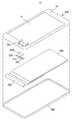
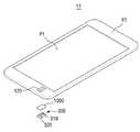
도 1을 참조하면, 본 발명의 일 실시에에 따른 표시장치(10)는 표시패널(400), 표시패널(400)의 하측에 배치되는 회로기판(500), 회로기판(500) 상에 배치되는 광센서부재(300), 표시패널(400) 및 회로기판(500)을 수납하는 하우징(600), 표시패널(400), 표시패널(400) 및 회로기판(500) 상에 배치된 커버윈도우(100) 및 커버윈도우(100)의 일측에 광센서부재(300)와 대응하도록 배치되는 편광부재(1000)를 포함한다.1, a
표시패널(400)은 영상을 표시할 수 있다. 표시패널(400)은 유기 발광 표시패널(OLED panel), 액정 표시패널(LCD panel), 전기영동 표시패널(EPD panel), 및 일렉트로웨팅 표시패널(EWD panel)과 같이 다양한 표시패널 등의 다양한 표시패널을 포함할 수 있으나, 이에 한정되는 것은 아니다.The
도 1에 도시된 바와 같이, 회로기판(500)은 표시패널(400)의 두께방향으로 표시패널(400)의 측면을 덮도록 배치될 수 있고, 표시패널(400)의 측면으로부터 연장되어 측면의 상측 모서리에 인접한 면과 하측 모서리에 인접한 면의 적어도 일부를 덮고 있을 수 있다. 더욱 구체적으로 설명하면, 회로기판(500)은 표시패널(400)의 커버윈도우(100)와 마주보는 면의 일측 모서리에 인접한 면의 일부분을 덮고 있으면서, 상기 일측 모서리에 인접한 표시패널(400)의 측면 및 상기 측면에 인접한 하면으로 연장되어 있을 수 있다.1, the
회로기판(500)은 표시패널(400)과 전기적으로 연결되어 있고, 표시패널(400)을 구동하는 구동소자, 신호를 처리하는 신호제어장치 및 전원장치(Switching Mode Supply, SMPS)를 포함할 수 있다.The
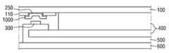
커버윈도우(100)는 표시패널(400) 상에 배치되며, 하우징(600)에 결합되어 하우징(600)과 함께 표시장치(10)의 외면을 구성할 수 있다. 표시패널(400)은 커버윈도우(100)에 결합될 수 있다.The
커버윈도우(100)는 평면상으로 표시패널(400)에서 투사된 영상이 표시되는 표시영역(P1) 및 표시영역(P1)을 둘러싸는 비표시영역(P2)을 포함할 수 있다. 비표시영역(P2)은 표시패널(400)에서 투사된 영상이 표시되지 않는 영역이다. 예를 들어, 표시영역(P1)에 대응하는 커버윈도우(100)의 일면에는 컬러층(110)이 배치되어 있지 않아서 광을 그대로 통과시킬 수 있고, 비표시영역(P2)에 대응하는 커버윈도우(100)의 일면에는 컬러층(110)이 배치되어 있어서, 광을 적어도 부분적으로 차단할 수 있다. 컬러층(110)이 불투명한 물질로 이루어진 경우, 입사되는 광을 완전히 차단할 수 있다.The
비표시영역(P2)의 광센서부재(300)와 중첩되는 영역에는 홀(120)이 정의될 수 있다. 홀(120)은 비표시영역(P2) 내에서 컬러층(110)에 의해 정의된다. 홀(120)은 커버윈도우(100)를 노출하기 때문에 광을 통과시킬 수 있다.A
도 1에는 홀(120)이 사각형인 것을 도시하였으나, 광이 통과할 수 있다면 형상에 제한되지 않고 원형, 삼각형, 타원형 및 불규칙한 형상일 수 있다.Although the
광센서부재(300)는 회로기판(500)의 커버윈도우(100)와 마주보는 면에 배치될 수 있다. 더욱 구체적으로 설명하면, 광센서부재(300)는 회로기판(500)의 커버윈도우(100)를 향하는 면에서 커버윈도우(100)의 비표시영역(P2)과 중첩되는 영역에 배치될 수 있다.The
하우징(600)은 표시패널(400) 및 회로기판(500)을 수납할 수 있다. 도 1에서는 1개의 부재로 구성된 하우징(400)을 예시적으로 도시하고 있다. 그러나, 하우징(400)은 2개 이상의 부재가 결합되어 구성될 수도 있다. 이하, 1개의 부재로 구성된 하우징을 중심으로 상세히 설명하기로 한다.The
하우징(600)은 표시패널(400) 및 회로기판(500) 이외에 배터리(미도시)와 같은 전원부를 더 수납할 수 있다.The
하우징(600)은 합성수지를 사출하여 형성될 수 있고, 금속 재질, 예컨대 스테인레스 스틸 또는 티타늄을 포함하여 형성될 수도 있으나, 이에 한정되는 것은 아니다.The
도 1 및 도 4를 참조하면, 컬러층(110)은 커버윈도우(100)의 일면 상에 배치되고, 비표시영역(P2)의 적어도 일부에 대응하게 배치된다. 컬러층(110)은 커버윈도우(100)의 타면 상으로 입사되는 광을 흡수하거나 반사시킨다. 도 4에서 1개의 층을 포함하는 컬러층(110)을 예시적으로 도시하고 있다. 그러나, 컬러층(110)은 2개 이상의 층을 포함할 수도 있다.1 and 4, the
홀(120)은 컬러층(110)에 의해 정의되고, 커버윈도우(100)를 노출하며, 광센서부재(300)에 대응하는 영역 내에 배치될 수 있다. 도 1 내지 도 8에서 광센서부재(300)에 대응하는 영역 내에 1개의 홀(120)이 배치되는 것을 예시적으로 도시하고 있다. 그러나 다른 실시예에서, 광센서부재(300)에 대응하는 영역 내에 2개의 홀(120)이 배치될 수도 있다. 이하, 광센서부재(300)에 대응하는 영역 내에 1개의 홀(120)이 배치되는 것을 중심으로 상세히 설명하기로 한다.The
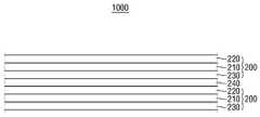
도 2 내지 도 3을 참조하면 커버윈도우(100)의 일측에 편광부재(1000)가 배치될 수 있다. 편광부재(1000)는 적층되어 있는 2개의 편광필름(200)을 포함한다.Referring to FIGS. 2 to 3, the polarizing
더욱 구체적으로 설명하면, 각각의 편광필름(200)은 적층되어 있는 편광자(210), 제1 보호층(220) 및 제2 보호층(230)을 포함할 수 있다. 편광자(210)의 일면에 제1 보호층(220)이 배치되고, 편광필름(200)의 타면에 제2 보호층(230)이 배치될 수 있다.More specifically, each
편광자(210)는 입사광 중 한쪽 방향으로 진동하는 광만 투과시키고 다른 방향으로 진동하는 광은 흡수하는 편광기능을 갖는다. 편광자(210)는 편광자(210)는 폴리 비닐 알코올(Poly Vinyl Alcohol, PVA)을 포함하여 이루어질 수 있다.The
제1 보호층(220) 및 제2 보호층(230)은 편광자(210)를 보호하거나 지지할 수 있다. 제1 보호층(220) 및 제2 보호층(230)에 의해 편광자(210)의 내구성, 기계적 강도, 내열 및 내습성이 향상될 수 있다.The
제1 보호층(220) 및 제2 보호층(230) 중 적어도 하나는 트리아세틸 셀룰로오스(TriAcetyl Cellulose, TAC)를 포함할 수 있다. 또한, 제1 보호층(220) 및 제2 보호층(230) 중 적어도 하나는 셀룰로오스 아세테이트 트리멜리테이트(Cellulose Acetate Trimellitate, CAT)를 포함할 수 있다. 예시적인 실시예에서, 제1 보호층(220)은 TAC로 이루어지고, 제2 보호층(230)은 CAT로 이루어질 수 있다.At least one of the first
도 2 및 도 3을 참조하면, 편광부재(1000)에 포함되어 있는 2개의 편광필름(200)중 어느 하나의 편광필름(200)의 편광축은 제1 편광방향(D1)을 향하고, 나머지 편광필름(200)의 편광축 방향은 제2 편광방향(D2)을 향한다.2 and 3, the polarization axis of one
이때, 제1 편광방향(D1)과 제2 편광방향(D2)이 동일 평면상에서 이루는 각도(a)는 45도 내지 90도일 수 있다. 0도 내지 90도 범위에서 각도(a)가 클수록 편광부재(1000)를 투과하는 가시광선의 양은 감소한다. 더욱 구체적으로 설명하면, 제1 편광방향(D1)과 제2 편광방향(D2)이 동일 평면상에서 이루는 각도(a)가 90도에 가까울수록 가시광선이 편광부재(1000)를 투과하는 양이 감소한다.At this time, the angle a formed by the first polarization direction D1 and the second polarization direction D2 on the same plane may be 45 degrees to 90 degrees. The larger the angle (a) is in the range of 0 to 90 degrees, the smaller the amount of visible light transmitted through the
한편, 적외선은 가시광선보다 파장이 길기 때문에 상대적으로 투과력이 좋고, 제1 편광방향(D1)과 제2 편광방향(D2)이 동일 평면상에서 이루는 각도(a)가 90도에 가깝더라도 편광부재(1000)를 잘 투과할 수 있다. 예컨대 본 발명의 일 실시예에 따른 표시장치(10)의 편광부재(1000)에 940nm 이상의 파장을 갖는 적외선을 출사하면 80% 이상의 투과율을 얻을 수 있다.On the other hand, since the infrared ray has a longer wavelength than the visible light and has relatively good transmission power and the angle a formed on the same plane by the first polarization direction D1 and the second polarization direction D2 is close to 90 degrees, ) Can be transmitted well. For example, when infrared ray having a wavelength of 940 nm or more is emitted to the
그 결과, 본 발명의 일 실시예에 따른 표시장치(10)의 편광부재(1000)는 가시광선 영역에서 낮은 투과율을 갖고, 높은 적외선 투과율을 갖는다. 이에 따라, 광센서부재(300)가 외부에 보이지 않는 상태에서, 광센서부재(300)가 편광부재(1000)를 통해 적외선을 주고 받을 수 있다.As a result, the polarizing
편광부재(1000)에 포함되어 있는 2개의 편광필름(200) 사이에 제1 접착층(240)이 배치될 수 있다. 제1 접착층(240)은 2개의 편광필름(200)을 접착시킬 수 있다. 제1 접착층(240)은 투명 접착층일 수 있다. 예를 들어, 제1 접착층(240)은 OCA(Optically clear adhesive)일 수 있다. 그러나, 이에 제한되지 않고, OCR(Optically clear resin)이 적용될 수도 있다.The first
예시적인 실시예에서, 제1 접착층은 PSA(Pressure Sensitive Adhesive)를 포함할 수 있다. PSA는 고분자 경화물을 포함할 수 있다. PSA는 점착제를 포함하여 필름 형태로 이루어져, 외부에서 제공되는 압력에 응답하여 점착 기능을 수행한다. PSA는 아크릴계나 고무계의 점착제, 혹은 상기 점착제에 질코니아 등의 미립자를 함유시킨 점착제를 포함할 수 있다.In an exemplary embodiment, the first adhesive layer may comprise PSA (Pressure Sensitive Adhesive). The PSA may comprise a polymeric cure. The PSA is made of a film including a pressure-sensitive adhesive, and performs an adhesive function in response to an externally supplied pressure. The PSA may include an acrylic or rubber pressure-sensitive adhesive, or a pressure-sensitive adhesive containing fine particles such as zirconia in the pressure-sensitive adhesive.
편광부재(1000)는 상술한 바와 같이, 2개의 편광필름(200)을 적층하여 제조되기 때문에 전체 영역에서 일정한 두께를 갖는다. 따라서, 적외선 인쇄층 대신 필름 형태로 제공되는 편광부재(1000)를 커버윈도우의 일측에 부착하여 사용함으로써, 광센서부재(300)에서 출사된 광의 난반사를 억제할 수 있다Since the
도 4를 참조하면, 커버윈도우(100)의 일면에 홀(120)을 정의하는 컬러층(110)이 배치되어 있다. 본 발명의 일 실시예에 따른 표시장치(10)의 편광부재(1000)는 홀(120)보다 큰 면적을 갖는다. 편광부재(1000)와 커버윈도우(100) 사이에 제2 접착층(250)이 배치됨으로써, 편광부재(1000)가 커버윈도우(100)에 부착될 수 있다. 도 4에는 제2 접착층(250)이 편광부재(1000) 상에 배치되어 있으나, 커버윈도우(100)의 일면에 배치되는 것도 가능하다. 편광부재(1000)는 홀(120)이 노출하는 커버윈도우(100) 상에 배치되고, 컬러층(110)의 홀(120)에 인접한 영역으로 연장 배치될 수 있다.Referring to FIG. 4, a
본 발명의 다른 실시예에 따른 편광부재(1100)는 도 5에 도시된 바와 같이, 홀(120)과 동일한 면적을 가질 수도 있다. 본 발명의 다른 실시예에 따른 편광부재(1100)는 홀(120)과 동일한 면적을 갖기 때문에 홀(120)이 노출하는 커버윈도우(100) 상에 배치되는 동시에 컬러층(110) 상으로 연장되지 않을 수 있다.The
도 4에 도시된 편광부재(1000)를 사용할 경우 부착되는 위치에 오차가 있더라도 일정 마진(margin)을 갖고 있기 때문에 커버윈도우(100)가 노출되지 않을 수 있으나, 도 5에 도시된 편광부재(1100)를 사용할 경우, 부착되는 위치에 오차가 있다면 커버윈도우(100)가 노출되는 불량이 발생할 수 있다는 단점이 있다. 그러나 도 5에 도시된 편광부재(1100)를 사용할 경우 도 4에 도시된 편광부재(1000)를 사용할 경우에 비해 편광부재(1100) 제조에 소요되는 재료를 절감할 수 있다.When the
도 1 및 도 6을 참조하면, 커버윈도우(100)의 일측에 광센서부재(300)가 배치되어 있고, 편광부재(1000)가 커버윈도우(100)의 일면에 배치될 수 있다. 더욱 구체적으로 설명하면, 커버윈도우(100)의 일측에 홀(120)에 대응하도록 광센서부재(300)가 배치되고, 커버윈도우(100)의 광센서부재(300)와 마주보는 면에 편광부재(1000)가 배치될 수 있다. 즉, 편광부재(1000)와 광센서부재(300)는 홀(120)과 중첩되는 영역에 배치될 수 있다. 표시패널(400), 회로기판(500), 및 하우징(600)은 상기에서 상세히 설명하였으므로 중복된 설명은 생략하기로 한다.1 and 6, a
도 7은 도 6의 표시장치의 변형예를 모식적으로 도시한 단면도이다.Fig. 7 is a cross-sectional view schematically showing a modification of the display device of Fig. 6;
도 7의 표시장치는 도 6의 표시장치와 유사하다. 다만, 회로기판(501)이 표시패널(400)의 측면을 감싸지 않고, 표시패널(400)의 하우징(600)과 마주보는 면에만 배치된 점에서 도 6의 표시장치와 상이하다. 이때, 광센서부재(300)는 회로기판(501)의 커버윈도우(100)와 마주보는 면 상에서 표시패널(400)이 배치되지 않은 영역에 배치될 수 있다.The display device of Fig. 7 is similar to the display device of Fig. 6 except that the
도 1, 도 4 및 도 8을 참조하면, 커버윈도우(100)의 일측에 광센서부재(300)가 배치되고, 커버윈도우(100)의 광센서부재(300)와 마주보는 면 상에 편광부재(1000)가 배치될 수 있다.1, 4, and 8, a
광센서부재(300)는 발광부(310)와 수광부(320)를 포함할 수 있다. 도 1 및 도 8에서 발광부(310)와 수광부(320)는 하나의 홀(120)에 대응하는 것을 도시하였으나, 본 발명의 또 다른 실시예에 따른 표시장치에서는 발광부(310)와 수광부(320)가 상이한 홀(120)에 각각 대응하도록 배치될 수 있다.The
발광부(310)는 홀(120)을 통하여 커버윈도우(100) 상측으로 광을 출사한다. 출사된 광의 일부는 인접한 사용자(700)에 의해 반사되어 홀(120)을 통하여 내부로 들어와 수방부(320)에 수신될 수 있다. 한편, 인접한 사용자(700)가 없는 경우에는 홀(120)을 통하여 출사된 광이 반사되어 되돌아오지 않기 때문에 광이 수광부(320)에 충분히 수신되지 않을 수 있다.The
예시적인 실시예에서, 수광부(320)는 가시광선 및 적외선을 동시에 수신할 수 있다. 적외선을 수신하여 상기와 같이 인접한 사용자(700)를 인식하는 동시에, 가시광선을 이용하여 조도를 측정할 수 있다.In the exemplary embodiment, the
도 9는 본 발명의 일 실시예에 따른 편광부재(1000)의 파장에 따른 투과율을 도시하는 그래프이다.9 is a graph showing the transmittance according to the wavelength of the
도 9를 참조하면, 본 발명의 일 실시예에 따른 편광부재(1000)는 940nm 이상의 파장을 갖는 적외선은 80% 이상 투과시키는 반면, 가시광선 및 자외선은 상대적으로 투과율이 낮다. 예컨대 가시광선의 투과율은 20% 미만일 수 있다. 그 결과, 광센서부재(300)가 외부에 보이지 않을 수 있고, 광센서부재(300)가 편광부재(1000)를 통해 적외선을 주고 받을 수 있다.Referring to FIG. 9, the polarizing
도 10은 본 발명의 일 실시예에 따른 표시장치의 전원 관리 장치의 구성도이다.10 is a configuration diagram of a power management apparatus of a display apparatus according to an embodiment of the present invention.
도 10을 참조하면, 본 발명의 일 실시예에 따른 표시장치(10)의 전원 관리 장치는 광센서부재(300), 통신모듈(810), 오디오 처리부(820), 저장부(830), 입력부(840), 표시부(850) 및 제어부(860)를 포함할 수 있다.10, a power management apparatus of a
광센서부재(300)는 사용자의 근접을 감지하는 역할을 수행한다. 본 발명의 일 실시예에 따른 광센서부재(300)는 포토 다이오드(photodiode) 기반의 광센서부재(300)일 수 있다. 광센서부재(300)는 발광부(310) 및 수광부(320)를 포함하며 발광부(310)는 LED(Light Emitting Diode)를 포함할 수 있고, 수광부(320)는 포토다이오드를 포함할 수 있다. 특히 발광부(310)는 IR LED(Infra-red Light Emitting Diode)로 구성될 수 있으며, 수광부(320)는 적외선을 흡수하는 포토 다이오드로 구성될 수 있다.The
수광부(320)는 흡수한 광을 전류(current)로 전환할 수 있으며, 전환된 전류를 ADC(Analog-to-Digital Converter)를 통해 ADC값으로 변환할 수 있다. 예시적인 실시예에서, ADC값은 16비트의 65536개의 카운트(count)값들로 구성될 수 있다. 수광부(320)는 발광부(310)에서 투사된 광이 사용자에 의해 반사되어 들어오는 광만을 측정할 수 있다. 수광부(320)는 측정된 수광량을 제어부(860)로 전달할 수 있다. 측정된 수광량은 제어부(860)가 사용자의 근접 여부를 판단하는 척도가 될 수 있다.The
통신부(810)는 표시장치의 무선 통신을 위한 데이터의 송수신 기능을 수행할 수 있다. 통신부(810)는 송신되는 신호의 주파수를 상승변환 및 증폭하는 RF송신기와, 수신되는 신호를 저잡음 증폭하고 주파수를 하강변환하는 RF수신기 등으로 구성될 수 있다. 또한, 통신부(810)는 무선 채널을 통해 데이터를 수신하여 제어부(860)로 출력하고, 제어부(860)로부터 출력된 데이터를 무선 채널을 통해 전송할 수 있다The
오디오 처리부(820)는 코덱으로 구성될 수 있으며, 코덱은 패킷 데이터 등을 처리하는 데이터 코덱과 음성 등의 오디오 신호를 처리하는 오디오 코덱을 포함할 수 있다. 오디오 처리부(820)는 디지털 오디오 신호를 오디오 코덱을 통해 아날로그 오디오 신호로 변환하여 스피커를 통해 재생하고, 마이크로부터 입력되는 아날로그 오디오 신호를 오디오 코덱을 통해 디지털 오디오 신호로 변환할 수 있다.The
저장부(830)는 표시장치의 동작에 필요한 프로그램 및 데이터를 저장하며 프로그램 영역과 데이터 영역으로 구분될 수 있다. 저장부(830)는 휘발성(volatile) 저장 매체 또는 비휘발성(nonvolatile) 저장 매체로 구성될 수 있으며, 양 저장 매체의 조합(combination)으로 구성될 수도 있다. 휘발성 저장 매체로는 RAM, DRAM, SRAM과 같은 반도체 메모리(semiconductor memory)가 포함되며, 비휘발성 저장 매체로는 하드 디스크(hard disk)가 포함될 수 있다.The
본 발명의 실시예에 따른 저장부(830)는 보상량 저장부를 포함할 수 있다. 보상량 저장부는 물체가 광센서부재(300)에 접근하지 않은 상태(오픈 상태)에서 측정되는 수광량의 범위와 이에 대응하는 보상량을 저장할 수 있다. 표시장치의 근접 인식 거리를 일정하게 유지시키기 위해서는 상황에 따라 근접 인식을 위해 필요한 기준값(근접 인식 임계 수광량)이 조절될 필요가 있다. 본 발명은 오픈 상태에서 수광량을 측정하고, 이를 기준으로 근접 인식 기준값을 재설정하는데, 여기서 '보상량'이란 오픈 상태에서 측정된 수광량으로부터 근접 인식 기준값을 산출하기 위해 필요한 수광량의 보상치에 해당할 수 있다.The
본 발명의 근접 인식 기준값은 사용자가 통화 호 발신을 위한 키 또는 통화 호 수신에 대한 응답을 위한 키를 입력할 때마다 재설정되며, 저장부(830)는 재설정되는 근접 인식 기준값을 저장할 수 있다.The proximity recognition reference value of the present invention is reset each time the user inputs a key for calling a call or a key for responding to a call reception, and the
입력부(840)는 표시장치를 제어하기 위한 사용자의 키 조작신호를 입력받아 제어부(860)로 전달할 수 있다. 표시장치가 터치스크린 기반의 표시장치인 경우, 입력부(840)는 표시부(850)와 일체형으로 구성될 수 있다. 입력부(840)는 사용자 입력에 따라 표시장치의 기능들을 실행하는 입력 신호를 생성하여 제어부(860)에 전달할 수 있다.The
표시부(850)는 액정표시장치(LCD, Liquid Crystal Display)로 형성될 수 있으며, 표시장치의 메뉴, 입력된 데이터, 기능 설정 정보 및 기타 다양한 정보를 사용자에게 시각적으로 제공할 수 있다. 예를 들어, 표시부(850)는 표시장치 부팅 화면, 대기 화면, 표시 화면, 통화 화면, 기타 어플리케이션 실행화면을 출력하는 기능을 수행할 수 있다.The
제어부(860)는 표시장치의 전반적인 동작 및 표시장치의 내부 블록들 간 신호 흐름을 제어할 수 있다. 제어부(860)는 입력부(840)를 통해 사용자의 키 입력(다이얼 모드에 진입하는 키, 다이얼 모드에 진입 후 숫자 키, 전화부 기능을 선택하는 키 또는 통화 호 수신에 응답하는 키 등)을 인식하면, 발광부(310)를 제어하여 광을 투사하고, 수광부(320)를 제어하여 발광부(310)에 의해 투사된 광에 대한 수광량을 측정할 수 있다. 수광부(320)는 측정된 수광량을 제어부(860)로 송신하고, 제어부(860)는 수광량을 수신하며, 수신된 수광량에 대응하는 보상량을 저장부(830)로부터 추출하며, 추출된 보상량을 수신된 수광량에 보상할 수 있다. 제어부(860)는 보상된 수광량을 근접 인식 기준값으로 설정하며, 설정된 근접 인식 기준값을 저장부(140)에 저장할 수 있다. 근접 인식 기준값을 설정한 후, 제어부(860)는 발광부(310)를 제어하여 광을 투사하고, 수광부(320)를 제어하여 발광부(310)에 의해 투사된 광에 대한 수광량을 측정하고, 측정된 수광량과 저장된 근접 인식 기준값을 비교하여 물체의 근접을 인식할 수 있다The
도 11은 본 발명의 일 실시예에 따른 표시장치의 전원 관리 방법을 도시하는 순서도이다.11 is a flowchart showing a power management method of a display apparatus according to an embodiment of the present invention.
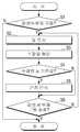
도 8 및 도 11을 참조하면, 표시장치(10)는 광센서부재(300)를 구동시킬 것인지 결정한다(S1). 예를 들어, 사용자가 통화를 시도하는 경우, 광센서부재(300)를 구동시킬 수 있다. 광센서부재(300)를 구동시키지 않는 것으로 결정한 경우, 표시장치는 본 알고리즘을 종료한다.8 and 11, the
광센서부재(300)를 구동시키는 경우, 표시장치(10)는 빛을 투사한다(S2). 광센서부재(300)를 구동시키면 광센서부재(300)에 포함된 발광부(310)는 광을 투사한다.When the
광을 투사한 후, 수광량을 확인한다(S3). 광센서부재(300)에 포함된 수광부(320)는 발광부(310)에서 투사된 광이 사용자에 의해 반사될 때 많은 양의 광을 수광할 수 있고, 발광부(310)에서 투사된 광이 사용자에 의해 반사되지 않을 때 상대적으로 적은 양의 광을 수광할 수 있다.After the light is projected, the amount of received light is confirmed (S3). The
이후, 상기 수광량과 기준값을 비교한다(S4). 수광량이 기준값보다 작은 경우 표시장치(10)는 사용자가 근접하지 않은 것으로 인식하고, 광센서부재(300) 구동을 종료할 것인지 결정한다(S6). 수광량이 기준값보다 크거나 같은 경우, 표시장치(10)는 근접 인식(S5) 단계로 진행하여 사용자가 근접한 것으로 인식한다. 예를 들어, 사용자가 근접한 것으로 인식한 경우, 표시장치(10)는 화면의 표시를 중단시킨다.Then, the received light amount is compared with a reference value (S4). If the amount of received light is smaller than the reference value, the
사용자가 근접한 것으로 인식한 다음, 표시장치(10)는 광센서부재(300)의 구동을 종료할 것인지 결정한다(S6). 예를 들어, 사용자가 통화를 시도할 때 광센서부재(300)가 구동되는 경우, 표시장치(10)는 사용자가 통화를 종료하였는지 확인한다. 표시장치는 사용자가 통화를 종료한 경우, 광센서부재(300)의 구동을 종료하는 것으로 결정한다. 한편, 표시장치(10)는 사용자가 통화중인 경우, 광센서부재(300) 구동을 종료하지 않는 것으로 결정한다.After recognizing that the user is close, the
광센서부재(300)의 구동을 종료하지 않는 것으로 결정한 경우, 표시장치(10)는 빛을 투사 하는 단계(S2)로 진행한다.If it is determined that the drive of the
광센서부재(300)의 구동을 종료하는 것으로 결정한 경우, 본 알고리즘은 종료된다. 예를 들어, 사용자가 근접한 것으로 인식(S5)하여 화면의 표시가 종료된 후, 사용자가 통화를 종료하여 광센서부재(300)의 구동이 종료되면, 화면의 표시가 활성화 될 수 있다.If it is determined to terminate driving of the
상기와 같은 전원 관리 방법을 실시하여 표시장치(10)는 사용자가 통화하는 동안 화면의 표시를 중단시킴으로써, 전력 소비량을 저감할 수 있다.By performing the power management method as described above, the
도 12는 도 2 및 도 3의 편광부재의 변형예를 모식적으로 도시한 단면도이다.12 is a cross-sectional view schematically showing a modified example of the polarizing member of Figs. 2 and 3. Fig.
도 12의 편광부재(1200)는 도 2 및 도 3의 편광부재(1000)와 유사하다. 다만, 도 2 및 도 3의 편광부재(1000)는 2개의 편광필름을 포함하는 반면, 3개의 편광필름(200)을 포함한다는 점에서 도 2 및 도 3의 편광부재(1000)와 상이하다. 편광자(210), 제1 보호층(220), 제2 보호층(230) 및 제1 접착층(240)은 상기에 상세히 설명하였으므로 중복된 설명은 생략하기로 한다.The
적층되어 있는 3개의 편광필름을 포함하는 편광부재(1200)의 편광축 방향은 상이할 수 있다. 도 2 및 도 3에 도시된 편광부재(1000)와 동일한 원리로 3개의 편광필름을 포함하는 편광부재(1200)는 자외선 및 가시광선 영역에서 낮은 투과율을 갖고 높은 적외선 투과율을 갖는다. 이에 따라, 광센서부재(300)가 외부에 보이지 않을 수 있고, 광센서부재(300)가 편광부재(1200)를 통해 적외선을 주고 받을 수 있다.The polarization axis direction of the
상술한 바와 같이, 편광부재(1200)는 3개의 편광필름(200)을 적층하여 제조되기 때문에 전체 영역에서 일정한 두께를 갖는다. 따라서, 적외선 인쇄층 대신 필름 형태로 제공되는 편광부재(1200)를 커버윈도우의 일측에 부착하여 사용함으로써, 광센서부재(300)에서 출사된 광의 난반사를 억제할 수 있다.As described above, since the
도 13은 도 1의 표시장치의 변형예를 모식적으로 도시한 사시도이다.Fig. 13 is a perspective view schematically showing a modification of the display device of Fig. 1; Fig.
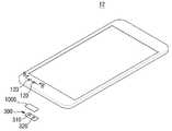
도 13의 표시장치(11)는 도 1의 표시장치(10)와 유사하다. 다만, 광센서부재(300)에 포함된 발광부(310)와 수광부(320)가 표시영역(P1)과 비표시영역(P2)의 경계를 이루는 모서리 중 상대적으로 길이가 긴 2개의 모서리의 길이방향으로 배열된 점에서 도 1에 도시된 표시장치(10)와 상이하다.The
도시된 바와 같이, 홀(120)은 발광부(310) 및 수광부(320)와 대응되는 위치와 형상을 가질 수 있다. 예시적인 실시예에서, 도 13에 도시된 바와 다르게, 발광부(310)와 수광부(320)의 위치가 서로 바뀌어 배치될 수도 있다.As shown in the figure, the
도 14는 도 1의 표시장치의 변형예를 모식적으로 도시한 사시도이다.Fig. 14 is a perspective view schematically showing a modification of the display device of Fig. 1; Fig.
도 14를 참조하면, 본 발명의 또 다른 실시예에 따른 표시장치(12)는 도 1의 표시장치(10)와 유사하다. 다만, 2개의 홀(120)을 포함하고, 1개의 홀(120)이 발광부(310)에 대응되는 위치에 배치되고, 나머지 1개의 홀(120)이 수광부(320)에 대응되는 위치에 배치되는 점에서 도 1의 표시장치(10)와 상이하다. 예시적인 실시예에서, 도 14에 도시된 바와 다르게, 발광부(310)와 수광부(320)의 위치가 서로 바뀌어 배치될 수도 있다. 편광부재(1000) 및 광센서부재(300)는 상기에서 상세히 설명하였으므로 중복된 설명은 생략하기로 한다.Referring to Fig. 14, the
도 15는 도 14의 표시장치를 도 14의 B-B’를 따라 절단한 단면도이다.Fig. 15 is a cross-sectional view of the display device of Fig. 14 taken along line B-B 'of Fig. 14;
도 14 및 도 15를 참조하면, 커버윈도우(100)의 일측에 컬러층(250)이 배치되고, 컬러층(250)은 2개의 홀(120)을 정의한다. 이때, 편광부재(1000)는 2개의 홀(120)이 노출하는 커버윈도우(100) 및 2개의 홀(120) 둘레에 인접한 컬러층(250) 상을 모두 덮도록 배치될 수 있다. 접착층(250)은 상기에서 상세히 설명하였으므로 중복된 설명은 생략하기로 한다.Referring to FIGS. 14 and 15, a
도 16은 도 15의 편광부재의 변형예를 모식적으로 도시한 단면도이다.16 is a cross-sectional view schematically showing a modified example of the polarizing member of Fig.
도 16의 편광부재(1300)는 도 15의 편광부재(1000)와 유사하다. 다만, 2개의 편광부재(1300)가 각각 2개의 홀(120)에 대응하도록 배치된 점에서 상이하다.The
이상 첨부된 도면을 참조하여 본 발명의 실시예들을 설명하였지만, 본 발명이 속하는 기술분야에서 통상의 지식을 가진 자는 본 발명의 그 기술적 사상이나 필수적인 특징을 변경하지 않고서 다른 구체적인 형태로 실시될 수 있다는 것을 이해할 수 있을 것이다. 그러므로 이상에서 기술한 실시예들은 모든 면에서 예시적인 것이며 한정적이 아닌 것으로 이해해야만 한다.While the present invention has been described in connection with what is presently considered to be practical exemplary embodiments, it is to be understood that the invention is not limited to the disclosed embodiments, but, on the contrary, You will understand. It is therefore to be understood that the above-described embodiments are illustrative in all aspects and not restrictive.
100 : 커버윈도우200 : 편광필름
300 : 광센서부재400 : 표시패널
500 : 회로기판P1 : 표시영역
P2 : 비표시영역1000 : 편광부재100: Cover window 200: Polarizing film
300: optical sensor member 400: display panel
500: circuit board P1: display area
P2: non-display area 1000: polarizing member
Claims (20)
Translated fromKorean발광부 및 수광부를 포함하고, 상기 커버윈도우의 일측에서 상기 비표시영역에 중첩되도록 배치되는 광센서부재;
상기 커버윈도우의 상기 광센서 부재와 마주보는 일면 상에서 상기 비표시영역과 중첩되는 영역에 형성되고, 상기 광센서부재와 대응하도록 1개의 홀(hole)을 정의하는 컬러층; 및
적층되어 있는 복수의 편광필름을 포함하고, 상기 홀이 노출하는 상기 커버윈도우의 일면 상에 배치되는 편광부재를 포함하는 표시장치.A cover window defining a display area and a non-display area surrounding the display area on the same plane;
An optical sensor member including a light emitting portion and a light receiving portion, the optical sensor member being disposed to overlap the non-display region at one side of the cover window;
A color layer formed in a region of the cover window that overlaps with the non-display region on one surface facing the photosensor member, the color layer defining one hole to correspond to the photosensor member; And
And a polarizing member including a plurality of polarizing films stacked and disposed on one surface of the cover window exposed by the hole.
상기 편광필름은 편광자;
상기 편광자의 일면에 형성된 제1 보호층; 및
상기 편광자의 타면에 형성된 제2 보호층을 포함하는 표시장치.The method according to claim 1,
Wherein the polarizing film comprises a polarizer;
A first protective layer formed on one surface of the polarizer; And
And a second protective layer formed on the other surface of the polarizer.
상기 제1 보호층 및 제2 보호층 중 적어도 하나는 트리아세틸 셀룰로오스(TriAcetyl Cellulose, TAC) 또는 셀룰로오스 아세테이트 트리멜리테이트(Cellulose Acetate Trimellitate, CAT)를 포함하는 표시장치.3. The method of claim 2,
Wherein at least one of the first protective layer and the second protective layer comprises TriAcetyl Cellulose (TAC) or Cellulose Acetate Trimellitate (CAT).
상기 편광부재는 제1 편광필름 및 제2 편광필름을 포함하고,
상기 제1 편광필름의 편광축 방향인 제1 편광방향과 상기 제2 편광필름의 편광축 방향인 제2 편광방향은 45도 내지 90도의 각도를 갖는 표시장치.The method according to claim 1,
Wherein the polarizing member comprises a first polarizing film and a second polarizing film,
Wherein a first polarization direction in a direction of a polarization axis of the first polarizing film and a second polarization direction in a direction of a polarization axis of the second polarizing film have an angle of 45 degrees to 90 degrees.
940nm 이상의 파장을 갖는 적외선의 상기 편광부재에 대한 투과율은 80% 이상인 표시장치.The method according to claim 1,
And a transmittance of the infrared ray having a wavelength of 940 nm or more to the polarizing member is 80% or more.
상기 복수의 편광필름 사이에 제1 접착층이 배치되는 표시장치.The method according to claim 1,
And a first adhesive layer is disposed between the plurality of polarizing films.
상기 홀이 노출하는 면과 상기 편광부재 사이에 제2 접착층이 배치되는 표시장치.The method according to claim 1,
And a second adhesive layer is disposed between the surface exposed by the hole and the polarizing member.
상기 편광부재는 상기 홀과 동일한 면적을 갖고 상기 홀과 대응되도록 배치되는 표시장치.The method according to claim 1,
Wherein the polarizing member has the same area as the hole and is arranged so as to correspond to the hole.
상기 편광부재는 상기 홀보다 넓은 면적을 갖고 상기 컬러층 상으로 연장 배치되는 표시장치.The method according to claim 1,
Wherein the polarizing member has a larger area than the hole and is extended on the color layer.
상기 발광부 및 수광부는 상기 표시영역과 상기 비표시영역의 경계를 이루는 모서리 중 상대적으로 길이가 짧은 2개의 모서리의 길이방향에 평행하게 배열된 표시장치.The method according to claim 1,
Wherein the light emitting portion and the light receiving portion are arranged parallel to a length direction of two corners relatively short in length among edges forming a boundary between the display region and the non-display region.
상기 발광부 및 수광부는 상기 표시영역과 상기 비표시영역의 경계를 이루는 모서리 중 상대적으로 길이가 긴 2개의 모서리의 길이방향에 평행하게 배열된 표시장치.The method according to claim 1,
Wherein the light emitting portion and the light receiving portion are arranged in parallel to the longitudinal direction of two relatively long corners among the corners forming the boundary between the display region and the non-display region.
발광부 및 수광부를 포함하고, 상기 커버윈도우의 일측에서 상기 비표시영역에 중첩되도록 배치되는 광센서부재;
상기 커버윈도우의 상기 광센서 부재와 마주보는 일면 상에서 상기 비표시영역과 중첩되는 영역에 형성되고, 상기 광센서부재와 대응하도록 2개의 홀(hole)을 정의하는 컬러층; 및
적층되어 있는 복수의 편광필름을 포함하고, 상기 홀이 노출하는 상기 커버윈도우의 일면 상에 배치되는 편광부재를 포함하되,
상기 2개의 홀은 상기 광센서부재에 포함된 발광부 및 수광부에 각각 하나씩 대응하도록 배치된 표시장치.A cover window defining a display area and a non-display area surrounding the display area on the same plane;
An optical sensor member including a light emitting portion and a light receiving portion, the optical sensor member being disposed to overlap the non-display region at one side of the cover window;
A color layer formed in an area overlapping the non-display area on one surface of the cover window facing the photosensor member, the color layer defining two holes corresponding to the photosensor member; And
And a polarizing member including a plurality of polarizing films stacked and disposed on one surface of the cover window through which the holes are exposed,
And the two holes are arranged so as to correspond to the light emitting portion and the light receiving portion included in the photosensor member, respectively.
상기 편광필름은 편광자;
상기 편광자의 일면에 형성된 제1 보호층; 및
상기 편광자의 타면에 형성된 제2 보호층을 포함하는 표시장치.13. The method of claim 12,
Wherein the polarizing film comprises a polarizer;
A first protective layer formed on one surface of the polarizer; And
And a second protective layer formed on the other surface of the polarizer.
상기 제1 보호층 및 제2 보호층 중 적어도 하나는 트리아세틸 셀룰로오스(TriAcetyl Cellulose, TAC) 또는 셀룰로오스 아세테이트 트리멜리테이트(Cellulose Acetate Trimellitate, CAT)를 포함하는 표시장치.14. The method of claim 13,
Wherein at least one of the first protective layer and the second protective layer comprises TriAcetyl Cellulose (TAC) or Cellulose Acetate Trimellitate (CAT).
상기 편광부재는 제1 편광필름 및 제2 편광필름을 포함하고,
상기 제1 편광필름의 편광축 방향인 제1 편광방향과 상기 제2 편광필름의 편광축 방향인 제2 편광방향은 45도 내지 90도의 각도를 갖는 표시장치.13. The method of claim 12,
Wherein the polarizing member comprises a first polarizing film and a second polarizing film,
Wherein a first polarization direction in a direction of a polarization axis of the first polarizing film and a second polarization direction in a direction of a polarization axis of the second polarizing film have an angle of 45 degrees to 90 degrees.
940nm 이상의 파장을 갖는 적외선의 상기 편광부재에 대한 투과율은 80% 이상인 표시장치.13. The method of claim 12,
And a transmittance of the infrared ray having a wavelength of 940 nm or more to the polarizing member is 80% or more.
상기 편광부재는 상기 홀과 동일한 면적을 갖고 상기 홀과 대응되도록 배치되는 표시장치.13. The method of claim 12,
Wherein the polarizing member has the same area as the hole and is arranged so as to correspond to the hole.
상기 편광부재는 상기 홀보다 넓은 면적을 갖고 상기 컬러층 상으로 연장 배치되는 표시장치.13. The method of claim 12,
Wherein the polarizing member has a larger area than the hole and is extended on the color layer.
상기 편광부재는 상기 2개의 홀이 노출하는 상기 커버윈도우의 일면들 상에 연속하여 배치되는 표시장치.13. The method of claim 12,
Wherein the polarizing member is disposed continuously on one side of the cover window from which the two holes are exposed.
상기 2개의 홀이 노출하는 상기 커버윈도우의 일면들 상에 각각 대응하는 2개의 편광부재가 배치되는 표시장치.13. The method of claim 12,
And two polarizing members corresponding to the respective ones of the cover windows on which the two holes are exposed are arranged.
Priority Applications (2)
| Application Number | Priority Date | Filing Date | Title |
|---|---|---|---|
| KR1020150001884AKR20160085037A (en) | 2015-01-07 | 2015-01-07 | Display device |
| US14/725,880US9874907B2 (en) | 2015-01-07 | 2015-05-29 | Display device |
Applications Claiming Priority (1)
| Application Number | Priority Date | Filing Date | Title |
|---|---|---|---|
| KR1020150001884AKR20160085037A (en) | 2015-01-07 | 2015-01-07 | Display device |
Publications (1)
| Publication Number | Publication Date |
|---|---|
| KR20160085037Atrue KR20160085037A (en) | 2016-07-15 |
Family
ID=56286493
Family Applications (1)
| Application Number | Title | Priority Date | Filing Date |
|---|---|---|---|
| KR1020150001884AWithdrawnKR20160085037A (en) | 2015-01-07 | 2015-01-07 | Display device |
Country Status (2)
| Country | Link |
|---|---|
| US (1) | US9874907B2 (en) |
| KR (1) | KR20160085037A (en) |
Cited By (2)
| Publication number | Priority date | Publication date | Assignee | Title |
|---|---|---|---|---|
| KR20200040953A (en)* | 2018-10-10 | 2020-04-21 | 삼성디스플레이 주식회사 | Cover window and display device including the same |
| KR20200113107A (en)* | 2019-03-22 | 2020-10-06 | 삼성디스플레이 주식회사 | Cover window and display module having the same |
Families Citing this family (10)
| Publication number | Priority date | Publication date | Assignee | Title |
|---|---|---|---|---|
| US10113973B2 (en) | 2017-01-20 | 2018-10-30 | Microsoft Technology Licensing, Llc | Infrared ink print testing for manufacturing |
| WO2018161753A1 (en) | 2017-03-07 | 2018-09-13 | 广东欧珀移动通信有限公司 | Terminal |
| KR102511474B1 (en) | 2017-09-13 | 2023-03-17 | 삼성디스플레이 주식회사 | display device |
| JP6973926B2 (en)* | 2017-10-16 | 2021-12-01 | アルパイン株式会社 | Front plate for display device and display device |
| CN207473963U (en)* | 2017-10-31 | 2018-06-08 | 昆山国显光电有限公司 | Effective display area has the display screen and display device of chamfered area |
| EP3983839B1 (en) | 2019-06-12 | 2025-08-06 | PPC Broadband Fiber Ltd. | Optical fiber connector |
| CN110264951B (en) | 2019-07-22 | 2021-01-22 | 京东方科技集团股份有限公司 | Organic electroluminescent display panel, display device and detection method |
| KR102763576B1 (en)* | 2019-07-24 | 2025-02-07 | 삼성전자주식회사 | Electronic device incluidng optical sensor module |
| KR102706216B1 (en)* | 2019-12-12 | 2024-09-13 | 삼성전자 주식회사 | Electronic device for controlling optical sensor module and operating method thereof |
| US20250201780A1 (en)* | 2023-12-19 | 2025-06-19 | Innolux Corporation | Display device |
Family Cites Families (15)
| Publication number | Priority date | Publication date | Assignee | Title |
|---|---|---|---|---|
| WO2008044463A1 (en)* | 2006-10-05 | 2008-04-17 | Konica Minolta Opto, Inc. | Liquid crystal display device of transverse electric field switching mode type |
| JP4778873B2 (en)* | 2006-10-20 | 2011-09-21 | 株式会社 日立ディスプレイズ | Liquid crystal display |
| US20100182538A1 (en)* | 2006-11-16 | 2010-07-22 | Yoshiki Takata | Liquid crystal display device and television receiver |
| JP5524501B2 (en) | 2008-06-30 | 2014-06-18 | 日東電工株式会社 | Polarizer, production method thereof, polarizing plate, optical film, and image display device |
| US8456586B2 (en)* | 2009-06-11 | 2013-06-04 | Apple Inc. | Portable computer display structures |
| US8384559B2 (en)* | 2010-04-13 | 2013-02-26 | Silicon Laboratories Inc. | Sensor device with flexible interface and updatable information store |
| US8567955B2 (en)* | 2011-03-24 | 2013-10-29 | Apple Inc. | Methods and apparatus for concealing sensors and other components of electronic devices |
| ITRM20110159A1 (en)* | 2011-03-29 | 2012-09-30 | Barberini S P A | POLARIZED COMPOSITE LENS WITH HIGH INFRARED PROTECTION. |
| KR101262252B1 (en) | 2011-10-18 | 2013-05-10 | 삼성디스플레이 주식회사 | Window substrate for display device and display device having the same |
| KR20130063570A (en) | 2011-12-07 | 2013-06-17 | 엘지전자 주식회사 | Mobile terminal and method for manufacturing the same |
| KR20140003046A (en) | 2012-06-29 | 2014-01-09 | 엘지이노텍 주식회사 | Touch window and fabricating method of the same, and lcd using the same |
| KR101884639B1 (en)* | 2012-07-20 | 2018-08-03 | 엘지디스플레이 주식회사 | Liquid crystal display device |
| JPWO2014038118A1 (en)* | 2012-09-07 | 2016-08-08 | パナソニックIpマネジメント株式会社 | Display device and display control system |
| US9088282B2 (en)* | 2013-01-25 | 2015-07-21 | Apple Inc. | Proximity sensors with optical and electrical sensing capabilities |
| CN104207760A (en)* | 2013-05-31 | 2014-12-17 | 义明科技股份有限公司 | Portable electronic device |
- 2015
- 2015-01-07KRKR1020150001884Apatent/KR20160085037A/ennot_activeWithdrawn
- 2015-05-29USUS14/725,880patent/US9874907B2/enactiveActive
Cited By (2)
| Publication number | Priority date | Publication date | Assignee | Title |
|---|---|---|---|---|
| KR20200040953A (en)* | 2018-10-10 | 2020-04-21 | 삼성디스플레이 주식회사 | Cover window and display device including the same |
| KR20200113107A (en)* | 2019-03-22 | 2020-10-06 | 삼성디스플레이 주식회사 | Cover window and display module having the same |
Also Published As
| Publication number | Publication date |
|---|---|
| US20160195905A1 (en) | 2016-07-07 |
| US9874907B2 (en) | 2018-01-23 |
Similar Documents
| Publication | Publication Date | Title |
|---|---|---|
| KR20160085037A (en) | Display device | |
| US11800746B2 (en) | Electronic devices with light sensors and displays | |
| US10963667B2 (en) | Under-screen biometric identification apparatus and electronic device | |
| US11263936B2 (en) | Electronic device including crack detection wiring | |
| CN110114779B (en) | Fingerprint identification device and electronic equipment | |
| KR102570864B1 (en) | Electronic apparatus | |
| KR102071734B1 (en) | Sensor-in-pixel display system with near infrared filter | |
| US10402018B2 (en) | Light-sensitive type touch panel, display device and touch positioning method | |
| TW201810119A (en) | Fingerprint identification device | |
| KR102269507B1 (en) | Display device | |
| WO2020211062A1 (en) | Fingerprint recognition apparatus and electronic device | |
| KR20170007670A (en) | Display apparatus | |
| KR20160022426A (en) | Display device | |
| KR20210126840A (en) | Sensing unit and display device having the same | |
| KR20210034822A (en) | Electronic device including displsy and camera unit | |
| KR20220027355A (en) | Display device | |
| CN110263747B (en) | Control method, electronic device, and non-volatile computer-readable storage medium | |
| US11300726B1 (en) | Display module and display device | |
| CN111294435B (en) | mobile terminal | |
| WO2024255622A1 (en) | Screen and electronic device | |
| WO2018028199A1 (en) | Touch control substrate and touch control display apparatus | |
| US20220263054A1 (en) | Window and display device having the same | |
| TWI607365B (en) | Handwriting interactive display device and handwriting interactive reading device | |
| CN115903098A (en) | Electronic device having anti-glare film with transparent openings | |
| CN115132069A (en) | Flexible display suitable for sensor under screen |
Legal Events
| Date | Code | Title | Description |
|---|---|---|---|
| PA0109 | Patent application | Patent event code:PA01091R01D Comment text:Patent Application Patent event date:20150107 | |
| PG1501 | Laying open of application | ||
| PC1203 | Withdrawal of no request for examination | ||
| WITN | Application deemed withdrawn, e.g. because no request for examination was filed or no examination fee was paid |