KR20160076298A - Touch input device - Google Patents
Touch input deviceDownload PDFInfo
- Publication number
- KR20160076298A KR20160076298AKR1020140186352AKR20140186352AKR20160076298AKR 20160076298 AKR20160076298 AKR 20160076298AKR 1020140186352 AKR1020140186352 AKR 1020140186352AKR 20140186352 AKR20140186352 AKR 20140186352AKR 20160076298 AKR20160076298 AKR 20160076298A
- Authority
- KR
- South Korea
- Prior art keywords
- electrode
- touch
- display module
- substrate
- pressure
- Prior art date
- Legal status (The legal status is an assumption and is not a legal conclusion. Google has not performed a legal analysis and makes no representation as to the accuracy of the status listed.)
- Granted
Links
Images


Classifications
- G—PHYSICS
- G06—COMPUTING OR CALCULATING; COUNTING
- G06F—ELECTRIC DIGITAL DATA PROCESSING
- G06F3/00—Input arrangements for transferring data to be processed into a form capable of being handled by the computer; Output arrangements for transferring data from processing unit to output unit, e.g. interface arrangements
- G06F3/01—Input arrangements or combined input and output arrangements for interaction between user and computer
- G06F3/03—Arrangements for converting the position or the displacement of a member into a coded form
- G06F3/041—Digitisers, e.g. for touch screens or touch pads, characterised by the transducing means
- G06F3/0414—Digitisers, e.g. for touch screens or touch pads, characterised by the transducing means using force sensing means to determine a position
- G—PHYSICS
- G06—COMPUTING OR CALCULATING; COUNTING
- G06F—ELECTRIC DIGITAL DATA PROCESSING
- G06F3/00—Input arrangements for transferring data to be processed into a form capable of being handled by the computer; Output arrangements for transferring data from processing unit to output unit, e.g. interface arrangements
- G06F3/01—Input arrangements or combined input and output arrangements for interaction between user and computer
- G06F3/03—Arrangements for converting the position or the displacement of a member into a coded form
- G06F3/041—Digitisers, e.g. for touch screens or touch pads, characterised by the transducing means
- G06F3/044—Digitisers, e.g. for touch screens or touch pads, characterised by the transducing means by capacitive means
- G06F3/0443—Digitisers, e.g. for touch screens or touch pads, characterised by the transducing means by capacitive means using a single layer of sensing electrodes
- G—PHYSICS
- G06—COMPUTING OR CALCULATING; COUNTING
- G06F—ELECTRIC DIGITAL DATA PROCESSING
- G06F2203/00—Indexing scheme relating to G06F3/00 - G06F3/048
- G06F2203/041—Indexing scheme relating to G06F3/041 - G06F3/045
- G06F2203/04103—Manufacturing, i.e. details related to manufacturing processes specially suited for touch sensitive devices
- G—PHYSICS
- G06—COMPUTING OR CALCULATING; COUNTING
- G06F—ELECTRIC DIGITAL DATA PROCESSING
- G06F2203/00—Indexing scheme relating to G06F3/00 - G06F3/048
- G06F2203/041—Indexing scheme relating to G06F3/041 - G06F3/045
- G06F2203/04111—Cross over in capacitive digitiser, i.e. details of structures for connecting electrodes of the sensing pattern where the connections cross each other, e.g. bridge structures comprising an insulating layer, or vias through substrate
Landscapes
- Engineering & Computer Science (AREA)
- General Engineering & Computer Science (AREA)
- Theoretical Computer Science (AREA)
- Human Computer Interaction (AREA)
- Physics & Mathematics (AREA)
- General Physics & Mathematics (AREA)
- Position Input By Displaying (AREA)
Abstract
Translated fromKoreanDescription
Translated fromKorean본 발명은 터치 입력 장치에 관한 것으로, 보다 상세하게는 디스플레이 모듈을 포함하는 터치 입력 장치로서 터치 위치 및 터치 압력의 크기를 검출할 수 있도록 구성된 터치 입력 장치에 관한 것이다.BACKGROUND OF THE
컴퓨팅 시스템의 조작을 위해 다양한 종류의 입력 장치들이 이용되고 있다. 예컨대, 버튼(button), 키(key), 조이스틱(joystick) 및 터치 스크린과 같은 입력 장치가 이용되고 있다. 터치 스크린의 쉽고 간편한 조작으로 인해 컴퓨팅 시스템의 조작시 터치 스크린의 이용이 증가하고 있다.Various types of input devices are used for the operation of the computing system. For example, an input device such as a button, a key, a joystick, and a touch screen is used. Due to the easy and simple operation of the touch screen, the use of the touch screen in the operation of the computing system is increasing.
터치 스크린은, 터치-감응 표면(touch-sensitive surface)을 구비한 투명한 패널일 수 있는 터치 센서 패널(touch sensor panel)을 포함하는 터치 입력 장치의 터치 표면을 구성할 수 있다. 이러한 터치 센서 패널은 디스플레이 스크린의 전면에 부착되어 터치-감응 표면이 디스플레이 스크린의 보이는 면을 덮을 수 있다. 사용자가 손가락 등으로 터치 스크린을 단순히 터치함으로써 사용자가 컴퓨팅 시스템을 조작할 수 있도록 한다. 일반적으로, 컴퓨팅 시스템은 터치 스크린 상의 터치 및 터치 위치를 인식하고 이러한 터치를 해석함으로써 이에 따라 연산을 수행할 수 있다.The touch screen may comprise a touch surface of a touch input device including a touch sensor panel, which may be a transparent panel having a touch-sensitive surface. Such a touch sensor panel may be attached to the front of the display screen such that the touch-sensitive surface covers the visible surface of the display screen. The user simply touches the touch screen with a finger or the like so that the user can operate the computing system. Generally, a computing system is able to recognize touch and touch locations on a touch screen and interpret the touch to perform operations accordingly.
이때, 디스플레이 모듈의 성능을 저하시키지 않으면서 터치 스크린 상의 터치에 따른 터치 위치뿐 아니라 터치의 압력 크기를 검출할 수 있는 터치 입력 장치에 대한 필요성이 야기되고 있다.At this time, there is a need for a touch input device capable of detecting not only a touch position corresponding to a touch on the touch screen but also a pressure magnitude of the touch without deteriorating the performance of the display module.
본 발명의 목적은 터치 스크린 상의 터치의 위치뿐 아니라 터치 압력의 크기를 검출할 수 있는 디스플레이 모듈을 포함하는 터치 입력 장치를 제공하는 것이다.It is an object of the present invention to provide a touch input device including a display module capable of detecting a position of a touch on a touch screen as well as a magnitude of a touch pressure.
본 발명의 또 다른 목적은 디스플레이 모듈의 시인성(visibility) 및 빛 투과율을 저하시킴이 없이 터치 위치 및 터치의 압력 크기를 검출할 수 있도록 구성된, 디스플레이 모듈을 포함하는 터치 입력 장치를 제공하는 것이다.It is still another object of the present invention to provide a touch input device including a display module configured to detect a touch position and a pressure magnitude of a touch without lowering the visibility and light transmittance of the display module.
본 발명의 또 다른 목적은 터치의 압력 크기 검출 정밀도가 개선된 터치 입력 장치를 제공하는 것이다.It is still another object of the present invention to provide a touch input device with improved pressure magnitude detection precision of a touch.
본 발명의 실시형태에 따른 터치 입력 장치는, 터치 표면에 대한 터치의 압력 검출이 가능한 터치 입력 장치로서, 기판; 및 디스플레이 모듈;을 포함하고, 상기 터치 표면에 대한 상기 터치에 따라 기준 전위층과의 거리가 변할 수 있는 위치에 배치된 전극을 더 포함하며, 상기 거리는 상기 터치의 압력 크기에 따라 달라질 수 있으며, 상기 전극은 상기 거리의 변화에 따른 전기적 신호를 출력할 수 있고, 상기 기준 전위층과 상기 전극 사이에 스페이서층이 위치할 수 있다.A touch input device according to an embodiment of the present invention is a touch input device capable of detecting pressure of a touch on a touch surface, comprising: a substrate; And an electrode arranged at a position where a distance from the reference potential layer can be changed according to the touch with respect to the touch surface, the distance being variable according to a pressure magnitude of the touch, The electrode may output an electrical signal according to the change of the distance, and a spacer layer may be positioned between the reference potential layer and the electrode.
본 발명에 따르면 터치 스크린 상의 터치의 위치뿐 아니라 터치 압력의 크기를 검출할 수 있는 디스플레이 모듈을 포함하는 터치 입력 장치를 제공할 수 있다.According to the present invention, it is possible to provide a touch input device including a display module capable of detecting a position of a touch on a touch screen as well as a magnitude of a touch pressure.
또한, 본 발명에 따르면, 디스플레이 모듈의 시인성(visibility) 및 빛 투과율을 저하시킴이 없이 터치 위치 및 터치의 압력 크기를 검출할 수 있도록 구성된, 디스플레이 모듈을 포함하는 터치 입력 장치를 제공할 수 있다.According to another aspect of the present invention, there is provided a touch input device including a display module configured to detect a touch position and a pressure magnitude of a touch without lowering the visibility and light transmittance of the display module.
또한, 본 발명에 따르면, 별도의 에어갭(air gap)을 제작함이 없이 제작 공정에 따라 기 존재하는 에어갭을 이용하여 터치 위치 및 터치의 압력 크기를 검출할 수 있도록 구성된, 디스플레이 모듈을 포함하는 터치 입력 장치를 제공할 수 있다.According to another aspect of the present invention, there is provided a display module including a display module configured to detect a touch position and a pressure magnitude of a touch using an existing air gap in accordance with a manufacturing process without manufacturing an additional air gap It is possible to provide a touch input device.
또한, 본 발명에 따르면 터치의 압력 크기 검출 정밀도가 개선된 터치 입력 장치를 제공할 수 있다.In addition, according to the present invention, it is possible to provide a touch input device with improved pressure magnitude detection accuracy of a touch.
도1은 본 발명의 실시예에 따른 정전 용량 방식의 터치 센서 패널 및 이의 동작을 위한 구성의 개략도이다.
도2a, 도2b 및 도2c는 본 발명의 실시예에 따른 터치 입력 장치에서 디스플레이 모듈에 대한 터치 센서 패널의 상대적인 위치를 예시하는 개념도이다.
도3은 본 발명의 제1실시형태에 따라 터치 위치 및 터치 압력을 검출할 수 있도록 구성된 터치 입력 장치의 단면도이다.
도4a 내지 도4f는 본 발명의 제2실시형태에 따른 터치 입력 장치를 예시한다.
도5a 내지 도5i는 본 발명의 제3실시형태에 따른 터치 입력 장치를 예시한다.
도6a 내지 도6i는 본 발명의 제4실시형태에 따른 터치 입력 장치를 예시한다.
도7a 내지 도7e는 본 발명의 실시예에 따른 압력 전극 패턴을 예시한다.
도8a 및 도8b는 본 발명에 따른 터치 입력 장치에서 터치 압력의 크기와 포화 면적 사이의 관계를 나타낸다.
도9a 내지 도9d는 본 발명의 실시예에 따른 압력 전극의 부착 구조를 예시한다.
도10a 및 도10b는 본 발명의 제5실시형태에 따른 터치 입력 장치를 예시한다.
도11a 및 도11b는 본 발명의 실시예에 따른 압력 전극의 부착 방법을 예시한다.
도12a 내지 도12c는 본 발명의 실시예에 따른 압력 전극을 터치 센싱 회로에 연결하는 방법을 예시한다.
도13a 내지 도13c는 본 발명의 실시예에 따라 압력 전극이 복수의 채널을 구성하는 경우를 예시한다.
도14는 본 발명의 실시형태에 따른 터치 입력 장치의 터치 표면 중심부를 비전도성 객체로 가압하는 실험을 수행하여, 객체의 그램중량에 따른 정전용량의 변화량을 표시하는 그래프이다.FIG. 1 is a schematic view of a capacitive touch sensor panel according to an embodiment of the present invention and a configuration for its operation.
FIGS. 2A, 2B, and 2C are conceptual diagrams illustrating relative positions of a touch sensor panel with respect to a display module in a touch input device according to an exemplary embodiment of the present invention.
3 is a cross-sectional view of a touch input device configured to detect a touch position and a touch pressure according to a first embodiment of the present invention.
4A to 4F illustrate a touch input device according to a second embodiment of the present invention.
5A to 5I illustrate a touch input device according to a third embodiment of the present invention.
6A to 6I illustrate a touch input device according to a fourth embodiment of the present invention.
7A to 7E illustrate a pressure electrode pattern according to an embodiment of the present invention.
8A and 8B show the relationship between the magnitude of the touch pressure and the saturated area in the touch input device according to the present invention.
9A to 9D illustrate an attaching structure of a pressure electrode according to an embodiment of the present invention.
10A and 10B illustrate a touch input device according to a fifth embodiment of the present invention.
11A and 11B illustrate a method of adhering a pressure electrode according to an embodiment of the present invention.
12A to 12C illustrate a method of connecting a pressure electrode to a touch sensing circuit according to an embodiment of the present invention.
13A to 13C illustrate a case where the pressure electrode constitutes a plurality of channels according to an embodiment of the present invention.
FIG. 14 is a graph showing an amount of change in capacitance according to the gram weight of an object by performing an experiment for pressing the center of the touch surface of the touch input device according to the embodiment of the present invention to a non-conductive object.
후술하는 본 발명에 대한 상세한 설명은, 본 발명이 실시될 수 있는 특정 실시예를 예시로서 도시하는 첨부 도면을 참조한다. 이들 실시예는 당업자가 본 발명을 실시할 수 있기에 충분하도록 상세히 설명된다. 본 발명의 다양한 실시예는 서로 다르지만 상호 배타적일 필요는 없음이 이해되어야 한다. 도면에서 유사한 참조부호는 여러 측면에 걸쳐서 동일하거나 유사한 기능을 지칭한다.The following detailed description of the invention refers to the accompanying drawings, which illustrate, by way of illustration, specific embodiments in which the invention may be practiced. These embodiments are described in sufficient detail to enable those skilled in the art to practice the invention. It should be understood that the various embodiments of the present invention are different, but need not be mutually exclusive. In the drawings, like reference numerals refer to the same or similar functions throughout the several views.
이하, 첨부되는 도면을 참조하여 본 발명의 실시예에 따른 터치 입력 장치를 설명한다. 이하에서는 정전용량 방식의 터치 센서 패널(100) 및 압력 검출 모듈(400)을 예시하나 임의의 방식으로 터치 위치 및/또는 터치 압력을 검출할 수 있는 터치 센서 패널(100) 및 압력 검출 모듈(400)이 적용될 수 있다.Hereinafter, a touch input device according to an embodiment of the present invention will be described with reference to the accompanying drawings. Hereinafter, the capacitive
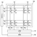
도1은 본 발명의 실시예에 따른 정전 용량 방식의 터치 센서 패널(100) 및 이의 동작을 위한 구성의 개략도이다. 도1을 참조하면, 본 발명의 실시예에 따른 터치 센서 패널(100)은 복수의 구동전극(TX1 내지 TXn) 및 복수의 수신전극(RX1 내지 RXm)을 포함하며, 상기 터치 센서 패널(100)의 동작을 위해 복수의 구동전극(TX1 내지 TXn)에 구동신호를 인가하는 구동부(120), 및 터치 센서 패널(100)의 터치 표면에 대한 터치에 따라 변화되는 정전용량 변화량에 대한 정보를 포함하는 감지신호를 수신하여 터치 및 터치 위치를 검출하는 감지부(110)를 포함할 수 있다.FIG. 1 is a schematic diagram of a capacitive
도1에 도시된 바와 같이, 터치 센서 패널(100)은 복수의 구동 전극(TX1 내지 TXn)과 복수의 수신 전극(RX1 내지 RXm)을 포함할 수 있다. 도1에서는 터치 센서 패널(100)의 복수의 구동전극(TX1 내지 TXn)과 복수의 수신전극(RX1 내지 RXm)이 직교 어레이를 구성하는 것으로 도시되어 있지만, 본 발명은 이에 한정되지 않으며, 복수의 구동전극(TX1 내지 TXn)과 복수의 수신전극(RX1 내지 RXm)이 대각선, 동심원 및 3차원 랜덤 배열 등을 비롯한 임의의 수의 차원 및 이의 응용 배열을 갖도록 할 수 있다. 여기서, n 및 m은 양의 정수로서 서로 같거나 다른 값을 가질 수 있으며 실시예에 따라 크기가 달라질 수 있다.As shown in FIG. 1, the
도1에 도시된 바와 같이, 복수의 구동전극(TX1 내지 TXn)과 복수의 수신전극(RX1 내지 RXm)은 각각 서로 교차하도록 배열될 수 있다. 구동전극(TX)은 제1축 방향으로 연장된 복수의 구동전극(TX1 내지 TXn)을 포함하고 수신전극(RX)은 제1축 방향과 교차하는 제2축 방향으로 연장된 복수의 수신전극(RX1 내지 RXm)을 포함할 수 있다.As shown in FIG. 1, the plurality of driving electrodes TX1 to TXn and the plurality of receiving electrodes RX1 to RXm may be arranged to cross each other. The driving electrode TX includes a plurality of driving electrodes TX1 to TXn extending in a first axis direction and a receiving electrode RX includes a plurality of receiving electrodes extending in a second axis direction intersecting the first axis direction RX1 to RXm).
본 발명의 실시예에 따른 터치 센서 패널(100)에서 복수의 구동전극(TX1 내지 TXn)과 복수의 수신전극(RX1 내지 RXm)은 서로 동일한 층에 형성될 수 있다. 예컨대, 복수의 구동전극(TX1 내지 TXn)과 복수의 수신전극(RX1 내지 RXm)은 절연막(미도시)의 동일한 면에 형성될 수 있다. 또한, 복수의 구동전극(TX1 내지 TXn)과 복수의 수신전극(RX1 내지 RXm)은 서로 다른 층에 형성될 수 있다. 예컨대, 복수의 구동전극(TX1 내지 TXn)과 복수의 수신전극(RX1 내지 RXm)은 하나의 절연막(미도시)의 양면에 각각 형성될 수도 있고, 또는 복수의 구동전극(TX1 내지 TXn)은 제1절연막(미도시)의 일면에 그리고 복수의 수신전극(RX1 내지 RXm)은 상기 제1절연막과 다른 제2절연막(미도시)의 일면상에 형성될 수 있다.In the
복수의 구동전극(TX1 내지 TXn)과 복수의 수신전극 (RX1 내지 RXm)은 투명 전도성 물질(예를 들면, 산화주석(SnO2) 및 산화인듐(In2O3) 등으로 이루어지는 ITO(Indium Tin Oxide) 또는 ATO(Antimony Tin Oxide)) 등으로 형성될 수 있다. 하지만, 이는 단지 예시일 뿐이며 구동전극(TX) 및 수신전극(RX)은 다른 투명 전도성 물질 또는 불투명 전도성 물질로 형성될 수도 있다. 예컨대, 구동전극(TX) 및 수신전극(RX)은 은잉크(silver ink), 구리(copper) 또는 탄소 나노튜브(CNT: Carbon Nanotube) 중 적어도 어느 하나를 포함하여 구성될 수 있다. 또한, 구동전극(TX) 및 수신전극(RX)는 메탈 메쉬(metal mesh)로 구현되거나 은나노(nano silver) 물질로 구성될 수 있다.A plurality of drive electrodes (TX1 to TXn) and a plurality of receiving electrodes (RX1 to RXm) is a transparent conductive material (e.g., tin oxide (SnO2) and indium oxide(In 2 O 3) ITO ( Indium Tin made of such Oxide) or ATO (antimony tin oxide)). However, this is merely an example, and the driving electrode TX and the receiving electrode RX may be formed of another transparent conductive material or an opaque conductive material. For example, the driving electrode TX and the receiving electrode RX may include at least one of silver ink, copper, or carbon nanotube (CNT). The driving electrode TX and the receiving electrode RX may be formed of a metal mesh or may be formed of a nano silver material.
본 발명의 실시예에 따른 구동부(120)는 구동신호를 구동전극(TX1 내지 TXn)에 인가할 수 있다. 본 발명의 실시예에서, 구동신호는 제1구동전극(TX1)부터 제n구동전극(TXn)까지 순차적으로 한번에 하나의 구동전극에 대해서 인가될 수 있다. 이러한 구동신호의 인가는 재차 반복적으로 이루어질 수 있다. 이는 단지 예시일 뿐이며, 실시예에 따라 다수의 구동전극에 구동신호가 동시에 인가될 수도 있다.The
감지부(110)는 수신전극(RX1 내지 RXm)을 통해 구동신호가 인가된 구동전극(TX1 내지 TXn)과 수신전극(RX1 내지 RXm) 사이에 생성된 정전용량(Cm: 101)에 관한 정보를 포함하는 감지신호를 수신함으로써 터치 여부 및 터치 위치를 검출할 수 있다. 예컨대, 감지신호는 구동전극(TX)에 인가된 구동신호가 구동전극(TX)과 수신전극(RX) 사이에 생성된 정전용량(CM: 101)에 의해 커플링된 신호일 수 있다. 이와 같이, 제1구동전극(TX1)부터 제n구동전극(TXn)까지 인가된 구동신호를 수신전극(RX1 내지 RXm)을 통해 감지하는 과정은 터치 센서 패널(100)을 스캔(scan)한다고 지칭할 수 있다.The
예를 들어, 감지부(110)는 각각의 수신전극(RX1 내지 RXm)과 스위치를 통해 연결된 수신기(미도시)를 포함하여 구성될 수 있다. 상기 스위치는 해당 수신전극(RX)의 신호를 감지하는 시간구간에 온(on)되어서 수신전극(RX)으로부터 감지신호가 수신기에서 감지될 수 있도록 한다. 수신기는 증폭기(미도시) 및 증폭기의 부(-)입력단과 증폭기의 출력단 사이, 즉 궤환 경로에 결합된 궤환 캐패시터를 포함하여 구성될 수 있다. 이때, 증폭기의 정(+)입력단은 그라운드(ground)에 접속될 수 있다. 또한, 수신기는 궤환 캐패시터와 병렬로 연결되는 리셋 스위치를 더 포함할 수 있다. 리셋 스위치는 수신기에 의해 수행되는 전류에서 전압으로의 변환을 리셋할 수 있다. 증폭기의 부입력단은 해당 수신전극(RX)과 연결되어 정전용량(CM: 101)에 대한 정보를 포함하는 전류 신호를 수신한 후 적분하여 전압으로 변환할 수 있다. 감지부(110)는 수신기를 통해 적분된 데이터를 디지털 데이터로 변환하는 ADC(미도시: analog to digital converter)를 더 포함할 수 있다. 추후, 디지털 데이터는 프로세서(미도시)에 입력되어 터치 센서 패널(100)에 대한 터치 정보를 획득하도록 처리될 수 있다. 감지부(110)는 수신기와 더불어, ADC 및 프로세서를 포함하여 구성될 수 있다.For example, the
제어부(130)는 구동부(120)와 감지부(110)의 동작을 제어하는 기능을 수행할 수 있다. 예컨대, 제어부(130)는 구동제어신호를 생성한 후 구동부(200)에 전달하여 구동신호가 소정 시간에 미리 설정된 구동전극(TX)에 인가되도록 할 수 있다. 또한, 제어부(130)는 감지제어신호를 생성한 후 감지부(110)에 전달하여 감지부(110)가 소정 시간에 미리 설정된 수신전극(RX)으로부터 감지신호를 입력받아 미리 설정된 기능을 수행하도록 할 수 있다.The
도1에서 구동부(120) 및 감지부(110)는 본 발명의 실시예에 따른 터치 센서 패널(100)에 대한 터치 여부 및 터치 위치를 검출할 수 있는 터치 검출 장치(미도시)를 구성할 수 있다. 본 발명의 실시예에 따른 터치 검출 장치는 제어부(130)를 더 포함할 수 있다. 본 발명의 실시예에 따른 터치 검출 장치는 터치 센서 패널(100)을 포함하는 터치 입력 장치(1000)에서 터치 센싱 회로인 터치 센싱 IC(touch sensing Integrated Circuit: 도12에서 150) 상에 집적되어 구현될 수 있다. 터치 센서 패널(100)에 포함된 구동전극(TX) 및 수신전극(RX)은 예컨대 전도성 트레이스(conductive trace) 및/또는 회로 기판상에 인쇄된 전도성 패턴(conductive pattern)등을 통해서 터치 센싱 IC(150)에 포함된 구동부(120) 및 감지부(110)에 연결될 수 있다. 터치 센싱 IC(150)는 전도성 패턴이 인쇄된 회로 기판, 예컨대 도12에서 160으로 표시되는 제1인쇄 회로 기판(이하에서, 제1PCB로 지칭) 상에 위치할 수 있다. 실시예에 따라 터치 센싱 IC(150)는 터치 입력 장치(1000)의 작동을 위한 메인보드 상에 실장되어 있을 수 있다.1, the driving
이상에서 살펴본 바와 같이, 구동전극(TX)과 수신전극(RX)의 교차 지점마다 소정 값의 정전용량(C)이 생성되며, 손가락과 같은 객체가 터치 센서 패널(100)에 근접하는 경우 이러한 정전용량의 값이 변경될 수 있다. 도1에서 상기 정전용량은 상호 정전용량(Cm)을 나타낼 수 있다. 이러한 전기적 특성을 감지부(110)에서 감지하여 터치 센서 패널(100)에 대한 터치 여부 및/또는 터치 위치를 감지할 수 있다. 예컨대, 제1축과 제2축으로 이루어진 2차원 평면으로 이루어진 터치 센서 패널(100)의 표면에 대한 터치의 여부 및/또는 그 위치를 감지할 수 있다.As described above, when a capacitance value C of a predetermined value is generated at each intersection of the driving electrode TX and the receiving electrode RX and an object such as a finger is close to the
보다 구체적으로, 터치 센서 패널(100)에 대한 터치가 일어날 때 구동신호가 인가된 구동전극(TX)을 검출함으로써 터치의 제2축 방향의 위치를 검출할 수 있다. 이와 마찬가지로, 터치 센서 패널(100)에 대한 터치시 수신전극(RX)을 통해 수신된 수신신호로부터 정전용량 변화를 검출함으로써 터치의 제1축 방향의 위치를 검출할 수 있다.More specifically, the position of the touch in the second axial direction can be detected by detecting the driving electrode TX to which the driving signal is applied when the touch to the
이상에서 터치 센서 패널(100)로서 상호 정전용량 방식의 터치 센서 패널이 상세하게 설명되었으나, 본 발명의 실시예에 따른 터치 입력 장치(1000)에서 터치 여부 및 터치 위치를 검출하기 위한 터치 센서 패널(100)은 전술한 방법 이외의 자기 정전용량 방식, 표면 정전용량 방식, 프로젝티드(projected) 정전용량 방식, 저항막 방식, 표면 탄성파 방식(SAW: surface acoustic wave), 적외선(infrared) 방식, 광학적 이미징 방식(optical imaging), 분산 신호 방식(dispersive signal technology) 및 음성 펄스 인식(acoustic pulse recognition) 방식 등 임의의 터치 센싱 방식을 이용하여 구현될 수 있다.Although the mutual capacitance type touch sensor panel has been described in detail as the
본 발명의 실시예에 따른 터치 입력 장치(1000)에서 터치 위치를 검출하기 위한 터치 센서 패널(100)은 디스플레이 모듈(200) 외부 또는 내부에 위치할 수 있다.The
본 발명의 실시예에 따른 터치 입력 장치(1000)의 디스플레이 모듈(200)은 액정표시장치(LCD: Liquid Crystal Display), PDP(Plasma Display Panel), 유기발광 표시장치(Organic Light Emitting Diode: OLED) 등에 포함된 디스플레이 패널일 수 있다. 이에 따라, 사용자는 디스플레이 패널에 표시된 화면을 시각적으로 확인하면서 터치 표면에 터치를 수행하여 입력 행위를 수행할 수 있다. 이때, 디스플레이 모듈(200)은 터치 입력 장치(100)의 작동을 위한 메인보드(main board) 상의 중앙 처리 유닛인 CPU(central processing unit) 또는 AP(application processor) 등으로부터 입력을 받아 디스플레이 패널에 원하는 내용을 디스플레이 하도록 하는 제어회로를 포함할 수 있다. 이러한 제어회로는 도11a 내지 13c에서 제2인쇄 회로 기판(210: 이하 제2PCB로 지칭)에 실장될 수 있다. 이때, 디스플레이 패널(200)의 작동을 위한 제어회로는 디스플레이 패널 제어 IC, 그래픽 제어 IC(graphic controller IC) 및 기타 디스플레이 패널(200) 작동에 필요한 회로를 포함할 수 있다.The
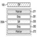
도2a, 도2b 및 도2c는 본 발명의 실시예에 따른 터치 입력 장치에서 디스플레이 모듈에 대한 터치 센서 패널의 상대적인 위치를 예시하는 개념도이다. 도2a 내지 도2c에서는 디스플레이 모듈(200) 내에 포함된 디스플레이 패널(200A)로서 LCD 패널이 도시되나, 이는 예시일 뿐이며 임의의 디스플레이 패널이 본 발명의 실시예에 따른 터치 입력 장치(1000)에 적용될 수 있다.FIGS. 2A, 2B, and 2C are conceptual diagrams illustrating relative positions of a touch sensor panel with respect to a display module in a touch input device according to an exemplary embodiment of the present invention. 2A to 2C, an LCD panel is shown as a
본원 명세서에서 도면부호 200A는 디스플레이 모듈(200)에 포함된 디스플레이 패널을 지칭할 수 있다. 도2에 도시된 바와 같이, LCD 패널(200A)은 액정 셀(liquid crystal cell)을 포함하는 액정 층(250), 액정 층(250)의 양단에 전극을 포함하는 제1글라스층(261)과 제2글라스층(262), 그리고 상기 액정 층(250)과 대향하는 방향으로서 상기 제1글라스층(261)의 일면에 제1편광층(271) 및 상기 제2글라스층(262)의 일면에 제2편광층(272)을 포함할 수 있다. 당해 기술분야의 당업자에게는, LCD 패널이 디스플레이 기능을 수행하기 위해 다른 구성을 더 포함할 수 있으며 변형이 가능함이 자명할 것이다.In the present specification,
도2a는, 터치 입력 장치(1000)에서 터치 센서 패널(100)이 디스플레이 모듈(200)의 외부에 배치된 것을 도시한다. 터치 입력 장치(1000)에 대한 터치 표면은 터치 센서 패널(100)의 표면일 수 있다. 도2a에서 터치 표면이 될 수 있는 터치 센서 패널(100)의 면은 터치 센서 패널(100)의 상부면이 될 수 있다. 또한, 실시예에 따라 터치 입력 장치(1000)에 대한 터치 표면은 디스플레이 모듈(200)의 외면이 될 수 있다. 도2a에서 터치 표면이 될 수 있는 디스플레이 모듈(200)의 외면은 디스플레이 모듈(200)의 제2편광층(272)의 하부면이 될 수 있다. 이때, 디스플레이 모듈(200)을 보호하기 위해서 디스플레이 모듈(200)의 하부면은 유리와 같은 커버층(미도시)으로 덮여있을 수 있다.FIG. 2A shows that the
도2b 및 2c는, 터치 입력 장치(1000)에서 터치 센서 패널(100)이 디스플레이 패널(200A)의 내부에 배치된 것을 도시한다. 이때, 도2b에서는 터치 위치를 검출하기 위한 터치 센서 패널(100)이 제1글라스층(261)과 제1편광층(271) 사이에 배치되어 있다. 이때, 터치 입력 장치(1000)에 대한 터치 표면은 디스플레이 모듈(200)의 외면으로서 도2b에서 상부면 또는 하부면이 될 수 있다. 도2c에서는 터치 위치를 검출하기 위한 터치 센서 패널(100)이 액정 층(250)에 포함되어 구현되는 경우를 예시한다. 또한, 실시예에 따라 디스플레이 패널(220A)을 동작하기 위한 전기적 소자들을 터치 센싱을 하는데 이용되도록 구현될 수도 있다. 이때, 터치 입력 장치(1000)에 대한 터치 표면은 디스플레이 모듈(200)의 외면으로서 도2c에서 상부면 또는 하부면이 될 수 있다. 도2b 및 도2c에서, 터치 표면이 될 수 있는 디스플레이 모듈(200)의 상부면 또는 하부면은 유리와 같은 커버층(미도시)으로 덮여있을 수 있다.Figs. 2B and 2C show that the
이상에서는 본 발명의 실시예에 따른 터치 센서 패널(100)에 대한 터치의 여부 및/또는 터치의 위치를 검출하는 것을 설명하였으나, 본 발명의 실시예에 따른 터치 센서 패널(100)을 이용하여 터치의 여부 및/또는 위치와 함께 터치의 압력의 크기를 검출할 수 있다. 또한 터치 센서 패널(100)과 별개로 터치 압력을 검출하는 압력 검출 모듈을 더 포함하여 터치의 압력 크기를 검출하는 것도 가능하다.Although the
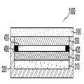
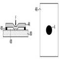
도3은 본 발명의 제1실시형태에 따라 터치 위치 및 터치 압력을 검출할 수 있도록 구성된 터치 입력 장치의 단면도이다.3 is a cross-sectional view of a touch input device configured to detect a touch position and a touch pressure according to a first embodiment of the present invention.
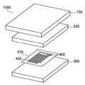
디스플레이 모듈(200)을 포함하는 터치 입력 장치(1000)에서 터치 위치를 검출하기 위한 터치 센서 패널(100) 및 압력 검출 모듈(400)은 디스플레이 모듈(200)의 전면에 부착될 수 있다. 이에 따라 디스플레이 모듈(200)의 디스플레이 스크린을 보호하고 터치 센서 패널(100)의 터치 검출 민감도를 높일 수 있다.The
이때, 압력 검출 모듈(400)은 터치 위치를 검출하기 위한 터치 센서 패널(100)과 별개로 동작할 수도 있는바, 예컨대, 압력 검출 모듈(400)은 터치 위치를 검출하기 위한 터치 센서 패널(100)과 독립적으로 압력만을 검출하도록 구성될 수 있다. 또한, 압력 검출 모듈(400)은 터치 위치를 검출하기 위한 터치 센서 패널(100)과 결합하여 터치 압력을 검출하도록 구성될 수 있다. 예컨대, 터치 위치를 검출하기 위한 터치 센서 패널(100)에 포함된 구동전극(TX)과 수신전극(RX) 중 적어도 하나의 전극은 터치 압력을 검출하는데 이용될 수 있다.In this case, the
도3에서 압력 검출 모듈(400)은 터치 센서 패널(100)과 결합하여 터치 압력을 검출할 수 있는 경우를 예시한다. 도2에서 압력 검출 모듈(400)은 상기 터치 센서 패널(100)과 디스플레이 모듈(200) 사이를 이격시키는 스페이서층(420)을 포함한다. 압력 검출 모듈(400)은 스페이서층(420)을 통해 터치 센서 패널(100)과 이격된 기준 전위층을 포함할 수 있다. 이때, 디스플레이 모듈(200)은 기준 전위층으로서 기능할 수 있다.In FIG. 3, the
기준 전위층은 구동전극(TX)과 수신전극(RX) 사이에 생성된 정전용량(101)에 변화를 야기할 수 있도록 하는 임의의 전위를 가질 수 있다. 예컨대, 기준 전위층은 그라운드(ground) 전위를 갖는 그라운드 층일 수 있다. 기준 전위층은 디스플레이 모듈(200)의 그라운드(ground) 층일 수 있다. 이때, 기준 전위층은 터치 센서 패널(100)의 2차원 평면과 평행한 평면을 가질 수 있다.The reference potential layer may have any potential that can cause a change in the
도3에 도시된 바와 같이, 터치 센서 패널(100)과 기준 전위층인 디스플레이 모듈(200)은 이격되어 위치한다. 이때, 터치 센서 패널(100)과 디스플레이 모듈(200)의 접착 방법의 차이에 따라 터치 센서 패널(100)과 디스플레이 모듈(200) 사이의 스페이서층(420)은 에어갭(air gap)으로 구현될 수 있다. 스페이서층(420)은 실시예에 따라 충격흡수물질로 이루어질 수 있다. 스페이서층(420)은 실시예에 따라 유전 물질(dielectric material)로 채워질 수 있다As shown in FIG. 3, the
이때, 터치 센서 패널(100)과 디스플레이 모듈(200)을 고정하기 위해서 양면 접착 테이프(430: DAT: Double Adhesive Tape)가 이용될 수 있다. 예컨대, 터치 센서 패널(100)과 디스플레이 모듈(200)은 각각의 면적이 포개어진 형태이고, 터치 센서 패널(100)과 터치 센서 패널(200) 각각의 가장자리 영역에서 양면 접착 테이프(430)를 통해서 두 개의 층이 접착되되 나머지 영역에서 터치 센서 패널(100)과 디스플레이 모듈(200)이 소정 거리(d)로 이격될 수 있다.At this time, a double adhesive tape (DAT: Double Adhesive Tape) may be used to fix the
일반적으로, 터치 센서 패널(100)의 휘어짐 없이 터치 표면을 터치하는 경우라도 구동전극(TX)과 수신전극(RX) 사이의 정전용량(101: Cm)이 변화한다. 즉, 터치 센서 패널(100)에 대한 터치시에 상호 정전용량(Cm: 101)이 기본 상호 정전용량에 비해 감소할 수 있다. 이는 손가락과 같은 도체인 객체가 터치 센서 패널(100)에 근접한 경우, 객체가 그라운드(GND) 역할을 하여 상호 정전용량(Cm: 101)의 프린징 정전용량(fringing capacitance)이 객체로 흡수되기 때문이다. 기본 상호 정전용량은 터치 센서 패널(100)에 대한 터치가 없는 경우에 구동전극(TX)과 수신전극(RX) 사이의 상호 정전용량의 값이다.Generally, the capacitance 101 (Cm) between the driving electrode TX and the receiving electrode RX changes even when the touch surface is touched without bending the
터치 센서 패널(100)의 터치 표면인 상부 표면을 객체로 터치 시 압력이 가해진 경우 터치 센서 패널(100)이 휘어질 수 있다. 이때, 구동전극(TX)과 수신전극(RX) 사이의 상호 정전용량(101: Cm)의 값은 더 감소할 수 있다. 이는, 터치 센서 패널(100)이 휘어져 터치 센서 패널(100)과 기준 전위층 사이의 거리가 d에서 d'로 감소함으로써 상기 상호 정전용량(101: Cm)의 프린징 정전용량이 객체뿐 아니라 기준 전위층으로도 흡수되기 때문이다. 터치 객체가 부도체인 경우에는 상호 정전용량(Cm)의 변화는 단순히 터치 센서 패널(100)과 기준 전위층 사이의 거리 변화(d-d')에만 기인할 수 있다.The
이상에서 살펴본 바와 같이, 디스플레이 모듈(200) 상에 터치 센서 패널(100) 및 압력 검출 모듈(400)을 포함하여 터치 입력 장치(1000)를 구성함으로써, 터치 위치뿐 아니라 터치 압력을 동시에 검출할 수 있다.As described above, by configuring the
하지만, 도3에 도시된 바와 같이, 터치 센서 패널(100)뿐 아니라 압력 검출 모듈(400)까지 디스플레이 모듈(200) 상부에 배치시키는 경우, 디스플레이 모듈의 디스플레이 특성이 저하되는 문제점이 발생한다. 특히, 디스플레이 모듈(200) 상부에 에어갭(420)을 포함하는 경우에 디스플레이 모듈의 시인성 및 빛 투과율이 저하될 수 있다.However, as shown in FIG. 3, when the
따라서, 이러한 문제점이 발생되는 것을 방지하기 위해서 터치 위치를 검출하기 위한 터치 센서 패널(100)과 디스플레이 모듈(200) 사이에 에어갭을 배치하지 않고, OCA(Optically Clear Adhesive)와 같은 접착제로 터치 센서 패널(100)과 디스플레이 모듈(200)이 완전 라미네이션(lamination)될 수 있다.Therefore, in order to prevent such a problem from occurring, an air gap is not disposed between the
도4a 내지 도4f는 본 발명의 제2실시형태에 따른 터치 입력 장치를 예시한다. 본 발명의 제2실시형태에 따른 터치 입력 장치(1000)에서 터치 위치를 검출하기 위한 터치 센서 패널(100)과 디스플레이 모듈(200) 사이가 접착제로 라미네이션된다. 이에 따라 터치 센서 패널(100)의 터치 표면을 통해 확인할 수 있는 디스플레이 모듈(200)의 디스플레이 색상 선명도, 시인성 및 빛 투과성이 향상될 수 있다.4A to 4F illustrate a touch input device according to a second embodiment of the present invention. The
도4a 내지 도4f를 참조한 설명에서, 본 발명의 제2실시형태에 따른 터치 입력 장치(1000)로서 터치 센서 패널(100)이 디스플레이 모듈(200) 상에 접착제로 라미네이션되어 부착된 것을 예시하나, 본 발명의 제2실시형태에 따른 터치 입력 장치(1000)는 터치 센서 패널(100)이 도2b 및 도2c 등에 도시된 바와 같이 디스플레이 모듈(200) 내부에 배치되는 경우도 포함할 수 있다. 보다 구체적으로, 도4a 및 도4b에서 터치 센서 패널(100)이 디스플레이 모듈(200)을 덮는 것이 도시되나, 터치 센서 패널(100)은 디스플레이 모듈(200) 내부에 위치하고 디스플레이 모듈(200)이 유리와 같은 커버층으로 덮인 터치 입력 장치(1000)가 본 발명의 제2실시형태로 이용될 수 있다. 4A to 4F illustrate that the
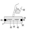
본 발명의 실시예에 따른 터치 입력 장치(1000)는 셀폰(cell phone), PDA(Personal Data Assistant), 스마트폰(smartphone), 태블랫 PC(tablet Personal Computer), MP3 플레이어, 노트북(notebook) 등과 같은 터치 스크린을 포함하는 전자 장치를 포함할 수 있다.The
본 발명의 실시예에 따른 터치 입력 장치(1000)에서 기판(300)은, 예컨대 터치 입력 장치(1000)의 최외곽 기구인 커버(320)와 함께 터치 입력 장치(1000)의 작동을 위한 회로기판 및/또는 배터리가 위치할 수 있는 실장공간 (310) 등을 감싸는 하우징(housing)의 기능을 수행할 수 있다. 이때, 터치 입력 장치(1000)의 작동을 위한 회로기판에는 메인보드(main board)로서 중앙 처리 유닛인 CPU(central processing unit) 또는 AP(application processor) 등이 실장되어 있을 수 있다. 기판(300)을 통해 디스플레이 모듈(200)과 터치 입력 장치(1000)의 작동을 위한 회로기판 및/또는 배터리가 분리되고, 디스플레이 모듈(200)에서 발생하는 전기적 노이즈가 차단될 수 있다.The
터치 입력 장치(1000)에서 터치 센서 패널(100) 또는 전면 커버층이 디스플레이 모듈(200), 기판(300), 및 실장공간(310)보다 넓게 형성될 수 있으며, 이에 따라 커버(320)가 터치 센서 패널(100)과 함께 디스플레이 모듈(200), 기판(300) 및 회로기판(310)을 감싸도록, 커버(320)가 형성될 수 있다.The
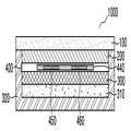
본 발명의 제2실시형태에 따른 터치 입력 장치(1000)는 터치 센서 패널(100)을 통해 터치 위치를 검출하고, 디스플레이 모듈(200)과 기판(300) 사이에 압력 검출 모듈(400)을 배치하여 터치 압력을 검출할 수 있다. 이때, 터치 센서 패널(100)은 디스플레이 모듈(200)의 내부 또는 외부에 위치할 수 있다. 압력 검출 모듈(400)은 예컨대, 에어갭(airgap)으로 이루어진 스페이서층(420)을 포함하여 구성되며, 이에 대해서는 도4b 내지 도4f를 참조하여 상세하게 살펴본다. 스페이서층(420)은 실시예에 따라 충격흡수물질로 이루어질 수 있다. 스페이서층(420)은 실시예에 따라 유전 물질(dielectric material)로 채워질 수 있다.The
도4b는 본 발명의 제2실시형태에 따른 터치 입력 장치의 사시도이다. 도4b에 도시된 바와 같이, 본 발명의 실시예에 따른 터치 입력 장치(1000)에서 압력 검출 모듈(400)는 디스플레이 모듈(200)과 기판(300)을 이격시키는 스페이서층(420) 및 스페이서층(420) 내에 위치하는 전극(450 및 460)을 포함할 수 있다. 이하에서, 터치 센서 패널(100)에 포함된 전극과 구분이 명확하도록, 압력을 검출하기 위한 전극(450 및 460)을 압력 전극(450 및 460)으로 지칭한다. 이때, 압력 전극(450 및 460)은 디스플레이 패널의 전면이 아닌 후면에 포함되므로 투명 물질뿐 아니라 불투명 물질로 구성되는 것도 가능하다.4B is a perspective view of the touch input device according to the second embodiment of the present invention. 4B, in the
이때, 스페이서층(420)을 유지하기 위해서 기판(300) 상부의 테두리를 따라 소정 두께를 갖는 접착 테이프(430)가 형성될 수 있다. 도4b에서 접착 테이프(430)는 기판(300)의 모든 테두리(예컨대, 4각형의 4면)에 형성된 것이 도시되나, 접착 테이프(440)는 기판(300)의 테두리 중 적어도 일부(예컨대, 4각형의 3면)에만 형성될 수도 있다. 실시예에 따라, 접착 테이프(430)는 기판(300)의 상부면 또는 디스플레이 모듈(200)의 하부면에 형성될 수도 있다. 접착 테이프(430)는 기판(300)과 디스플레이 모듈(200)을 동일한 전위로 만들 수 있도록 전도성 테이프일 수 있다. 또한, 접착 테이프(430)는 양면 접착 테이프일 수 있다. 본 발명의 실시예에서 접착 테이프(430)는 탄성이 없는 물질로 구성될 수 있다. 본 발명의 실시예에서, 디스플레이 모듈(200)에 압력이 인가되는 경우 디스플레이 모듈(200)이 휘어질 수 있으므로 접착 테이프(430)가 압력에 따라 형체의 변형이 없더라도 터치 압력의 크기를 검출할 수 있다.At this time, an
도4c는 본 발명의 실시예에 따른 압력 전극 패턴을 포함하는 터치 입력 장치의 단면도이다. 도4c에 도시된 바와 같이, 본 발명의 실시예에 따른 압력 전극(450, 460)은 스페이서층(420) 내로서 기판(300)상에 형성될 수 있다.4C is a cross-sectional view of a touch input device including a pressure electrode pattern according to an embodiment of the present invention. 4c, the
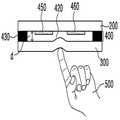
압력 검출을 위한 압력 전극은 제1전극(450)과 제2전극(460)을 포함할 수 있다. 이때, 제1전극(450)과 제2전극(460) 중 어느 하나는 구동전극일 수 있고 나머지 하나는 수신전극일 수 있다. 구동전극에 구동신호를 인가하고 수신전극을 통해 감지신호를 획득할 수 있다. 전압이 인가되면, 제1전극(450)과 제2전극(460) 사이에 상호 정전용량이 생성될 수 있다.The pressure electrode for pressure detection may include a
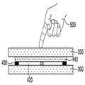
도4d는 도4c에 도시된 터치 입력 장치(1000)에 압력이 인가된 경우의 단면도이다. 디스플레이 모듈(200)의 하부면은 노이즈 차폐를 위해 그라운드(ground) 전위를 가질 수 있다. 객체(500)를 통해 터치 센서 패널(100)의 표면에 압력을 인가하는 경우 터치 센서 패널(100) 및 디스플레이 모듈(200)은 휘어지거나 눌릴 수 있다. 이에 따라 그라운드 전위면과 압력 전극 패턴(450, 460) 사이의 거리(d)가 d'로 감소할 수 있다. 이러한 경우, 상기 거리(d)의 감소에 따라 디스플레이 모듈(200)의 하부면으로 프린징 정전용량이 흡수되므로 제1전극(450)과 제2전극(460) 사이의 상호 정전용량은 감소할 수 있다. 따라서, 수신전극을 통해 획득되는 감지신호에서 상호 정전용량의 감소량을 획득하여 터치 압력의 크기를 산출할 수 있다.4D is a cross-sectional view of the
본 발명의 실시예에 따른 터치 입력 장치(100)에서, 디스플레이 모듈(200)은 압력을 인가하는 터치에 따라 휘어지거나 눌릴 수 있다. 디스플레이 모듈(200)은 터치에 따라 변형을 나타내도록 휘어지거나 눌릴 수 있다. 실시예에 따라 디스플레이 모듈(200)이 휘어지거나 눌릴 때 가장 큰 변형을 나타내는 위치는 상기 터치 위치와 일치하지 않을 수 있으나, 디스플레이 모듈(200)은 적어도 상기 터치 위치에서 휘어짐을 나타낼 수 있다. 예컨대, 터치 위치가 디스플레이 모듈(200)의 테두리 및 가장자리 등에 근접하는 경우 디스플레이 모듈(200)이 휘어지거나 눌리는 정도가 가장 큰 위치는 터치 위치와 다를 수 있으나, 디스플레이 모듈(200)은 적어도 상기 터치 위치에서 휘어짐 또는 눌림을 나타낼 수 있다.In the
이때, 기판(300)의 상부면 또한 노이즈 차폐를 위해 그라운드 전위를 가질 수 있다. 따라서, 기판(300)과 압력 전극(450, 460)이 단락(short circuit)되는 것을 방지하기 위해서 압력 전극(450, 460)은 절연층(470) 상에 형성될 수 있다. 도9는 본 발명의 실시예에 따른 압력 전극의 부착 구조를 예시한다. 도9a를 참조하여 설명하면, 압력 전극(450, 460)은 기판(300) 상에 제1절연층(470)을 위치시킨 후 압력 전극(450, 460)을 형성하여 구성될 수 있다. 또한, 실시예에 따라 압력 전극(450, 460)이 형성된 제1절연층(470)을 기판(300) 상에 부착하여 형성할 수 있다. 또한, 실시예에 따라 압력 전극은, 기판(300) 또는 기판(300)상의 제1절연층(470) 위에 압력 전극 패턴에 상응하는 관통 구멍을 갖는 마스크(mask)를 위치시킨 후 전도성 스프레이(spray)를 분사함으로써 형성될 수 있다.At this time, the upper surface of the
또한, 디스플레이 모듈(200)의 하부면이 그라운드 전위를 갖는 경우 기판(300) 상에 위치한 압력 전극(450, 460)과 디스플레이 모듈(300)이 단락되는 것을 방지하기 위해서 압력 전극(450, 460)은 추가의 제2절연층(471)으로 압력 전극(450, 460)을 덮을 수 있다. 또한, 제1절연층(470) 상에 형성된 압력 전극(450, 460)을 추가의 제2절연층(471)으로 덮은 후, 일체형으로 기판(300) 상에 부착하여 압력 검출 모듈(400)을 형성할 수 있다.When the lower surface of the
도9a를 참조하여 설명된 압력 전극(450, 460)의 부착 구조 및 방법은 압력 전극(450, 460)이 디스플레이 모듈(200)에 부착되는 경우에도 적용될 수 있다. 압력 전극(450, 460)이 디스플레이 모듈(200)에 부착되는 경우는 도4e와 관련하여 더욱 자세히 설명된다.The attachment structure and method of the
또한, 터치 입력 장치(1000)의 종류 및/또는 구현 방식에 따라, 압력 전극(450, 460)이 부착되는 기판(300) 또는 디스플레이 모듈(200)이 그라운드 전위를 나타내지 않거나 약한 그라운드 전위를 나타낼 수 있다. 이러한 경우, 본 발명의 실시예에 따른 터치 입력 장치(1000)는 기판(300) 또는 디스플레이 모듈(200)과 절연층(470) 사이에 그라운드 전극(ground electrode: 미도시)을 더 포함할 수 있다. 실시예에 따라, 그라운드 전극과 기판(300) 또는 디스플레이 모듈(200) 사이에는 또 다른 절연층(미도시)을 더 포함할 수도 있다. 이때, 그라운드 전극(미도시)은 압력 전극인 제1전극(450)과 제2전극(460) 사이에 생성되는 정전용량의 크기가 너무 커지는 것을 방지할 수 있다.Depending on the type and / or implementation of the
이상에서 설명한 압력 전극(450, 460) 형성 및 부착 방법은 이하의 실시예에도 동일하게 적용될 수 있다.The method of forming and attaching the
도4e는 본 발명의 실시예에 따른 압력(450, 460)이 디스플레이 모듈(200)의 하부면 상에 형성되는 경우를 예시한다. 이때, 기판(300)은 그라운드 전위를 가질 수 있다. 따라서, 터치 센서 패널(100)의 터치 표면을 터치함에 따라 기판(300)과 압력 전극(450, 460) 사이의 거리(d)가 감소하고, 결과적으로 제1전극(450)과 제2전극(460) 사이의 상호 정전용량의 변화를 야기할 수 있다.4E illustrates a case where
도7은 본 발명의 실시예에 따른 압력 전극 패턴을 예시한다. 도7a 내지 도7c에서는 제1전극(450)과 제2전극(460)이 기판(300) 상부 또는 디스플레이 모듈(200)의 하부면 상에 형성된 경우를 도시한다. 제1전극(450)과 제2전극(460) 사이의 정전용량은 제1전극(450) 및 제2전극(460)과 기준전위층(디스플레이 모듈(200) 또는 기판(300)) 사이의 거리에 따라 달라질 수 있다.7 illustrates a pressure electrode pattern according to an embodiment of the present invention. 7A to 7C illustrate the case where the
제1전극(450)과 제2전극(460) 사이의 상호 정전용량이 변화함에 따라 터치 압력의 크기를 검출할 때, 검출 정확도를 높이기 위해서 필요한 정전용량 범위를 생성하도록 제1전극(450)과 제2전극(460)의 패턴을 형성할 필요가 있다. 제1전극(450)과 제2전극(460)이 서로 마주하는 면적이 크거나 길이가 길수록 생성되는 정전용량의 크기가 커질 수 있다. 따라서, 필요한 정전용량 범위에 따라 제1전극(450)과 제2전극(460) 사이의 마주하는 면적의 크기, 길이 및 형상 등을 조절하여 설계할 수 있다. 도7b 및 도7c에는, 제1전극(450)과 제2전극(460)이 동일한 층에 형성되는 경우로서 제1전극(450)과 제2전극(460)이 서로 마주하는 길이가 상대적으로 길도록 압력 전극이 형성된 경우를 예시한다.The
이상에서는, 제1전극(450)과 제2전극(460)은 동일한 층에 형성된 것으로 도시되나, 제1전극(450)과 제2전극(460)은 실시예에 따라 서로 다른 층으로 구현되어도 무방하다. 도9b는 제1전극(450)과 제2전극(460)이 서로 다른 층에 구현된 경우의 부착 구조를 예시한다. 도9b에 예시된 바와 같이, 제1전극(450)은 제1절연층(470) 상에 형성되고 제2전극(460)은 제1전극(450) 상에 위치하는 제2절연층(471) 상에 형성될 수 있다. 실시예에 따라, 제2전극(460)은 제3절연층(472)으로 덮일 수 있다. 이때, 제1전극(450)과 제2전극(460)은 서로 다른 층에 위치하므로 서로 오버랩(overlap)되도록 구현될 수 있다. 예컨대, 제1전극(450)과 제2전극(460)은 도1을 참조하여 설명된 터치 센서 패널(100)에 포함된 MXN의 구조로 배열된 구동전극(TX)과 수신전극(RX)의 패턴과 유사하게 형성될 수 있다. 이때, M 및 N은 1 이상의 자연수 일 수 있다.Although the
이상에서 터치 압력은 제1전극(450)과 제2전극(460) 사이의 상호 정전용량의 변화로부터 검출되는 것이 예시된다. 하지만, 압력 전극(450, 460)이 제1전극(450)과 제2전극(460) 중 어느 하나의 압력 전극만을 포함하도록 구성될 수 있으며, 이러한 경우 하나의 압력 전극과 그라운드층(디스플레이 모듈(200) 또는 기판(300)) 사이의 정전용량 변화를 검출함으로써 터치 압력의 크기를 검출할 수도 있다.It is exemplified that the touch pressure is detected from the change of mutual capacitance between the
예컨대, 도4c에서 압력 전극은 제1전극(450)만을 포함하여 구성될 수 있으며, 이때 디스플레이 모듈(200)과 제1전극(450) 사이의 거리 변화에 따라 야기되는 제1전극(450)과 디스플레이 모듈(200) 사이의 정전용량 변화로부터 터치 압력의 크기를 검출할 수 있다. 터치 압력이 커짐에 따라 거리(d)가 감소하므로 디스플레이 모듈(200)과 제1전극(450) 사이의 정전용량은 터치 압력이 증가할수록 커질 수 있다. 이는 도4e와 관련된 실시예에도 동일하게 적용될 수 있다. 이때, 압력 전극은, 상호 정전용량 변화량 검출 정밀도를 높이기 위해 필요한, 빗살 형태 또는 삼지창 형상을 가질 필요는 없으며, 도7d에 예시된 바와 같이 판(예컨대, 사각판) 형상을 가질 수 있다.4C, the pressure electrode may include only the
도9c는 압력 전극이 제1전극(450)만을 포함하여 구현된 경우의 부착 구조를 예시한다. 도9c에 예시된 바와 같이, 제1전극(450)은 기판(300) 또는 디스플레이 모듈(200) 상에 위치한 제1절연층(470) 상에 형성될 수 있다. 또한, 실시예에 따라 제1전극(450)은 제2절연층(471)으로 덮일 수 있다.9C illustrates an attachment structure when the pressure electrode is implemented to include only the
도4f는 압력 전극(450, 460)이 스페이서층(420) 내로서 기판(300)의 상부면 및 디스플레이 모듈(200)의 하부면 상에 형성된 경우를 예시한다. 압력 검출을 위한 압력 전극 패턴은 제1전극(450)과 제2전극(460)을 포함할 수 있다. 이때, 제1전극(450)과 제2전극(460) 중 어느 하나는 기판(300) 상에 형성되고 나머지 하나는 디스플레이 모듈(200)의 하부면 상에 형성될 수 있다. 도4f에서는 제1전극(450)이 기판(300) 상에 형성되고 제2전극(460)이 디스플레이 모듈(200)의 하부면상에 형성된 것을 예시한다.4F illustrates the case where the
객체(500)를 통해 터치 센서 패널(100)의 표면에 압력을 인가하는 경우 터치 센서 패널(100) 및 디스플레이 모듈(200)은 휘어지거나 눌릴 수 있다. 이에 따라 제1전극(450)과 제2전극(460) 사이의 거리(d)가 감소할 수 있다. 이러한 경우, 상기 거리(d)의 감소에 따라 제1전극(450)과 제2전극(460) 사이의 상호 정전용량은 증가할 수 있다. 따라서, 수신전극을 통해 획득되는 감지신호에서 상호 정전용량의 증가량을 획득하여 터치 압력의 크기를 산출할 수 있다. 이때, 제1전극(450) 및 제2전극(460)에 대한 압력 전극 패턴은 각각 도7d에 예시된 바와 같은 형상을 가질 수 있다. 즉, 도4f에서 제1전극(450)과 제2전극(460)은 서로 다른 층에 형성되므로, 제1전극(450) 및 제2전극(460)은 빗살형상 또는 삼지창 형상을 가질 필요는 없으며 판형상(예컨대, 사각판형상)을 가질 수 있다.When pressure is applied to the surface of the
도9d는 제1전극(450)이 기판(300) 상에 부착되고 제2전극(460)이 디스플레이 모듈(200)에 부착된 경우의 부착 구조를 예시한다. 도9d에 예시된 바와 같이, 제1전극(450)은 기판(300) 상에 형성된 제1절연층(470-2) 상에 위치하고, 제1전극(450)은 제2절연층(471-2)에 의해 덮여 있을 수 있다. 또한, 제2전극(460)은 디스플레이 모듈(200)의 하부면 상에 형성된 제1절연층(470-1) 상에 위치하고, 제2전극(460)은 제2절연층(471-1)에 의해 덮여 있을 수 있다.9D illustrates an attachment structure when the
도9a와 관련하여 설명된 바와 마찬가지로, 압력 전극(450, 460)이 부착되는 기판(300) 또는 디스플레이 모듈(200)이 그라운드 전위를 나타내지 않거나 약한 그라운드 전위를 나타내는 경우, 도9a 내지 도9d에서 제1절연층(470, 470-1, 470-2) 사이에 그라운드 전극(미도시)을 더 포함할 수 있다. 이때, 그라운드 전극(미도시)과 압력 전극(450, 460)이 부착되는 기판(300) 또는 디스플레이 모듈(200) 사이에는 추가의 절연층(미도시)을 더 포함할 수 있다.
9A to 9D, when the
도5a 내지 도5i는 본 발명의 제3실시형태에 따른 터치 입력 장치를 예시한다. 본 발명의 제3실시형태는 도4a 내지 도4f를 참조하여 설명된 제2실시형태와 유사하며 이하에서는 그 차이점을 위주로 설명한다.5A to 5I illustrate a touch input device according to a third embodiment of the present invention. The third embodiment of the present invention is similar to the second embodiment described with reference to Figs. 4A to 4F, and the difference will be mainly described below.
도5a는 본 발명의 제3실시형태에 따른 터치 입력 장치의 단면도이다.5A is a cross-sectional view of a touch input device according to a third embodiment of the present invention.
본 발명의 제2실시형태에 따른 터치 입력 장치(1000)에서는 별도의 스페이서층 및/또는 기준 전위층을 제작함이 없이 디스플레이 모듈(200) 내 또는 외부에 존재하는 에어갭(air gap) 및/또는 전위층을 사용하여 터치 압력을 검출할 수 있으며 이에 대해서는 도5b 내지 도5i를 참조하여 상세하게 살펴본다.In the
도5b는 본 발명의 제3실시형태에 따른 터치 입력 장치(1000)에 포함될 수 있는 디스플레이 모듈(200)의 예시적인 단면도이다. 도5b에서는 디스플레이 모듈(200)로서 LCD 모듈을 예시한다. 도5b에 도시된 바와 같이, LCD 모듈(200)은 LCD 패널(200A)과 백라이트 유닛(200B: backlight unit)을 포함하여 구성될 수 있다. LCD 패널(200A)은 그 자체가 발광하지 못하고 다만 빛을 차단 내지 투과를 시키는 기능을 수행한다. 따라서, LCD 패널(200A)의 하부에는 광원이 위치하여 LCD 패널(200A)에 빛을 비추어 화면에는 밝음과 어두움뿐 아니라 여러 가지 다양한 색상을 갖는 정보를 표현하게 된다. LCD 패널(200A)은 수동소자로서 자체 발광하지 못하므로, 후면에 균일한 휘도 분포를 갖는 광원이 요구된다. LCD 패널(200A) 및 백라이트 유닛(200B)의 구조 및 기능은 공지된 기술이며 이하에서 간단히 살펴본다.5B is an exemplary cross-sectional view of a
LCD 패널(200A)을 위한 백라이트 유닛(200B)은 수개의 광학적 부품(optical part)을 포함할 수 있다. 도5b에서 백라이트 유닛(200B)은 광확산 및 광향상 시트(231), 도광판(232) 및 반사판(240)을 포함할 수 있다. 이때, 백라이트 유닛(200B)은 선광원(linear light source) 또는 점광원(point light source)등의 형태로서 도광판(232)의 후면 및/또는 측면에 배치된 광원(미도시)을 포함할 수 있다. 실시예에 따라, 도광판(232)과 광확산 및 광향상 시트(231)의 가장 자리에 지지부(233)를 더 포함할 수 있다.The backlight unit 200B for the
도광판(232: light guide plate)은 일반적으로 선광원 또는 점광원의 형태인 광원(미도시)으로부터 광들을 면광원 형태로 변환하여 LCD 패널(200A)로 향하게 하는 역할을 할 수 있다.The
도광판(232)에서 방출되는 광의 일부가 LCD 패널(200A)의 반대면으로 방출되어 손실될 수 있다. 반사판(240)은 이러한 손실된 광을 도광판(232)으로 재입사 시킬 수 있도록 도광판(232) 하부에 위치하며 반사율이 높은 물질로 구성될 수 있다.A part of the light emitted from the
광확산 및 광향상 시트(231)는 확산시트(diffuser sheet) 및/또는 프리즘 시트(prism sheet)를 포함할 수 있다. 확산시트는 도광판(232)으로부터 입사되는 광을 확산시키는 역할을 한다. 예컨대, 도광판(232)의 패턴(pattern)에 의하여 산란된 빛은 직접 눈으로 들어오기 때문에 도광판(232)의 패턴이 그대로 비치게 될 수 있다. 심지어 이러한 패턴은 LCD 패널(200A)을 장착한 후에도 확연하게 감지할 수 있으므로 확산시트는 이러한 도광판(232)의 패턴을 상쇄시키는 역할을 수행할 수 있다.The light diffusion and
확산시트를 지나면 광 휘도는 급격히 떨어지게 된다. 따라서, 광을 다시 포커스(focus)시켜 광 휘도를 향상시키도록 프리즘 시트가 포함될 수 있다.The light brightness rapidly drops after passing through the diffusion sheet. Thus, a prism sheet can be included to focus light again to improve light brightness.
백라이트 유닛(200B)은 기술의 변화, 발전 및/또는 실시예에 따라 전술한 구성과 다른 구성을 포함할 수 있으며, 또한 전술한 구성 이외에 추가적인 구성을 더 포함할 수 있다. 또한, 본 발명의 실시예에 따른 백라이트 유닛(200B)은 예컨대, 백라이트 유닛(200B)의 광학적 구성을 외부의 충격이나 이물 유입에 따른 오염 등으로부터 보호하기 위해서 보호 시트(protection sheet)를 프리즘 시트 상부에 더 포함할 수 있다. 또한, 백라이트 유닛(200B)은 광원으로부터의 광 손실을 최소화하기 위해서 실시예에 따라 램프 커버(lamp cover)를 더 포함할 수 있다. 또한, 백라이트 유닛(200B)은 백라이트 유닛(200B)의 주요 구성인 도광판(232), 시트(231) 및 램프(미도시) 등이 허용치수에 맞게 정확하게 형합이 가능하도록 하는 형태를 유지하게 해주는 프레임(frame)을 더 포함할 수도 있다. 또한, 전술한 구성 각각은 2개 이상의 별개의 부분으로 이루어질 수 있다. 예컨대, 프리즘 시트는 2개의 프리즘 시트로 구성될 수도 있다.The backlight unit 200B may include a configuration different from the configuration described above according to changes, developments, and / or embodiments of the technology, and may further include additional configurations in addition to the configurations described above. In order to protect the optical structure of the backlight unit 200B from contamination due to external impact or foreign matter inflow, for example, the backlight unit 200B according to the embodiment of the present invention may include a protection sheet, As shown in FIG. In addition, the backlight unit 200B may further include a lamp cover according to an embodiment in order to minimize light loss from the light source. The backlight unit 200B is a frame that allows the
이때, 도광판(232)과 반사판(240) 사이에는 재1에어갭(220-2)이 존재하도록 구성될 수 있다. 이에 따라 도광판(232)으로부터 반사판(240)으로의 손실광이 반사판(240)을 통해 다시 도광판(232)으로 재입사될 수 있다. 이때, 에어갭(220-2)을 유지할 수 있도록 도광판(233)과 반사판(240) 사이로서 가장자리에는 양면 접착 테이프(221-2)가 포함될 수 있다.At this time, a material air gap 220-2 may exist between the
또한, 실시예에 따라 백라이트 유닛(200B)는 LCD 패널(200A)과 제2에어갭(220-1)을 사이에 두고 위치할 수 있다. 이는 LCD 패널(200A)로부터의 충격이 백라이트 유닛(200B)으로 전달되는 것을 방지하기 위함이다. 이때, 에어갭(220-1)을 유지할 수 있도록 백라이트 유닛(200B)과 LCD 패널(200A) 사이로서 가장자리에는 양면 접착 테이프(221-1)가 포함될 수 있다.Also, according to the embodiment, the backlight unit 200B may be positioned between the
이상에서 살펴본 바와 같이, 디스플레이 모듈(200)은 자체적으로 제1에어갭(220-2) 및/또는 제2에어갭(220-1)과 같은 에어갭을 포함하여 구성될 수 있다. 또는 광확산 및 광향상 시트(231)의 복수의 레이어들 사이에 에어갭이 포함될 수 있다. 이상에서는 LCD 모듈의 경우에 대해서 설명하였으나, 다른 디스플레이 모듈의 경우에도 구조 내에 에어갭을 포함할 수 있다.As described above, the
따라서, 본 발명의 제3실시형태에 따른 터치 입력 장치(1000)는 압력 검출을 위해 별도의 스페이서층을 제작함이 없이 디스플레이 모듈(200) 내 또는 외에 이미 존재하는 에어갭을 사용할 수 있다. 스페이서층으로 이용되는 에어갭은 도5b를 참조하여 설명되는 제1에어갭(220-2) 및/또는 제2에어갭(220-1)뿐 아니라 디스플레이 모둘(200) 내에 포함되는 임의의 에어갭일 수 있다. 또는 디스플레이 모듈(200) 외부에 포함되는 에어갭일 수 있다. 이와 같이, 압력을 검출할 수 있는 터치 입력 장치(1000)를 제조함으로써 제조 비용을 절감하고 및/또는 제조 공정을 간소화할 수 있다. 도5c에는 본 발명의 제3실시형태에 따른 터치 입력 장치의 사시도이다. 도5c에서는 도4b에 도시된 제2실시형태의 그것과 달리 스페이서층(420)을 유지하기 위한 양면 접착 테이프(430)가 포함되지 않을 수 있다.Therefore, the
도5d는 제3실시형태에 따른 터치 입력 장치의 단면도를 예시한다. 도5a에 도시된 바와 같이, 압력 전극(450, 460)은 디스플레이 모듈(200)과 기판(300) 사이로서 기판(300)상에 형성될 수 있다. 도5d 내지 도5i에서 편의를 위해 압력 전극(450, 460)의 두께가 과장되어 두껍게 도시되나, 압력 전극(450, 460)은 시트(sheet) 형태로 구현될 수 있으므로 해당 두께는 매우 작을 수 있다. 마찬가지로, 디스플레이 모듈(200)과 기판(300) 사이의 간격 또한 과장되어 넓게 도시되었으나, 이 둘 사이의 간격 또한 매우 작은 간격을 갖도록 구현될 수 있다. 도5d 및 도5e에서 압력 전극(450, 460)이 기판(300) 상에 형성된 것을 나타내기 위해서 압력 전극(450, 460)과 디스플레이 모듈(200) 사이가 이격되도록 도시하였으나 이는 단지 설명을 위한 것이며 이들 사이는 이격되지 않도록 구현될 수도 있다.5D illustrates a cross-sectional view of the touch input device according to the third embodiment. 5A, the
이때, 도5d에서는 디스플레이 모듈(200)이 스페이서층(220) 및 기준 전위층(270)을 포함하는 것으로 도시된다.5D, the
스페이서층(220)은 도5b를 참조하여 설명된 바와 같이 디스플레이 모듈(200)의 제조시에 포함되는 제1에어갭(220-2) 및/또는 제2에어갭(220-1)일 수 있다. 디스플레이 모듈(220)이 하나의 에어갭을 포함하는 경우 해당 하나의 에어갭이 스페이서층(220)의 기능을 수행할 수 있으며, 디스플레이 모듈(220)이 복수 개의 에어갭을 포함하는 경우 해당 복수개의 에어갭이 통합적으로 스페이서층(220)의 기능을 수행할 수 있다. 도5d, 도5e, 도5h 및 도5i에서는 기능적으로 하나의 스페이서층(220)을 포함하는 것으로 도시된다.The
본 발명의 실시예에 따른, 터치 입력 장치(1000)는 도2a 내지 도2c에서 디스플레이 모듈(200) 내부로서 스페이서층(220)보다 상부에 기준 전위층(270)을 포함할 수 있다. 이러한 기준 전위층(270) 또한 디스플레이 모듈(200)의 제조시에 자체적으로 포함되는 그라운드 전위층일 수 있다. 예컨대, 도2a 내지 도2c에 도시된 디스플레이 패널(200A)에서 제1편광층(271)과 제1글라스층(261) 사이에 노이즈(noise) 차폐를 위한 전극(미도시)을 포함할 수 있다. 이러한 차폐를 위한 전극은 ITO로 구성될 수 있으며 그라운드 역할을 수행할 수 있다. 이와 같은 기준 전위층(270)은 디스플레이 모듈(200) 내부로서 상기 기준 전위층(270)과 압력 전극(450, 460) 사이에 스페이서층(220)이 위치하도록 하는 임의의 곳에 위치할 수 있으며, 이상에서 예시한 차폐 전극 이외의 임의의 전위를 갖는 전극이 기준 전위층(270)으로 이용될 수 있다. 예컨대, 기준 전위층(270)은 디스플레이 모듈(200)의 공통 전극 전위(Vcom)층일 수 있다.The
특히, 터치 입력 장치(1000)를 포함하는 장치의 두께를 얇게 하려는 노력의 일환으로서 별도의 커버 또는 프레임(frame)을 통해 디스플레이 모듈(200)을 싸도록 구성하지 않을 수 있다. 이러한 경우 기판(300)과 마주하는 디스플레이 모듈(200)의 하부면은 반사판(340) 및/또는 부도체일 수 있다. 이러한 경우 디스플레이 모듈(200) 하부면은 그라운드 전위를 가질 수 없다. 이와 같이 디스플레이 모듈(200) 하부면이 기준 전위층으로서 기능할 수 없는 경우에도 본 발명의 실시예에 따른 터치 압력 장치(1000)를 이용하면 디스플레이 모듈(200) 내부에 위치하는 임의의 전위층을 기준 전위층(270)으로 이용하여 압력을 검출할 수 있다.In particular, as an effort to reduce the thickness of the device including the
도5e는 도5d에 도시된 터치 입력 장치(1000)에 압력이 인가된 경우의 단면도이다. 객체(500)를 통해 터치 센서 패널(100)의 표면에 압력을 인가하는 경우 터치 센서 패널(100) 및 디스플레이 모듈(200)은 휘어지거나 눌릴 수 있다. 이때, 디스플레이 모듈(200) 내에 위치한 스페이서층(220)에 의해 기준 전위층(270)과 압력 전극 패턴(450, 460) 사이의 거리(d)가 d'로 감소할 수 있다. 이러한 경우, 상기 거리(d)의 감소에 따라 기준 전위층(270)으로 프린징 정전용량이 흡수되므로 제1전극(450)과 제2전극(460) 사이의 상호 정전용량은 감소할 수 있다. 따라서, 수신전극을 통해 획득되는 감지신호에서 상호 정전용량의 감소량을 획득하여 터치 압력의 크기를 산출할 수 있다.5E is a cross-sectional view of the
본 발명의 실시예에 따른 터치 입력 장치(1000)에서, 디스플레이 모듈(200)은 압력을 인가하는 터치에 따라 휘어지거나 눌릴 수 있다. 이때, 도5e에 도시된 바와 같이 스페이서층(220)으로 인해 스페이서층(220) 하부에 위치한 층(예컨대, 반사판)의 휘어짐 또는 눌림은 없거나 감소될 수 있다. 도5e에서는 디스플레이 모듈(200)의 최하부에서는 휘어짐 또는 눌림이 전혀 없는 것으로 도시되었으나 이는 예시일뿐이며 디스플레이 모듈(200)의 최하부에서도 휘어짐 또는 눌림이 있을 수 있으나 스페이서층(220)을 통해 그 정도가 완화될 수 있다.In the
제3실시형태에 따른 압력전극의 부착구조는 제2실시형태를 참조하여 설명된 것과 동일하므로 이하에서 생략한다.The mounting structure of the pressure electrode according to the third embodiment is the same as that described with reference to the second embodiment, and will not be described below.
도5f는 도5d를 참조하여 설명한 실시예의 변형예에 따른 압력 전극 패턴을 포함하는 터치 입력 장치의 단면도이다. 도5f에서는 스페이서층(420)이 디스플레이 모듈(200)과 기판(300) 사이에 위치하는 경우를 예시한다. 디스플레이 모듈(200)을 포함하는 터치 입력 장치(1000)를 제조할 때 디스플레이 모듈(200)과 기판(300) 사이는 완전 부착되지 않으므로 에어갭420)이 발생할 수 있다. 여기서, 이러한 에어갭(420)을 터치 압력 검출을 위한 스페이서층으로 이용함으로써 터치 압력 검출을 위해 일부러 스페이서층을 제작하는 시간/비용이 절감될 수 있다. 도5f 및 도5g에서는 스페이서층으로 이용되는 에어갭(220)이 디스플레이 모듈(200) 내부에 위치하지 않는 것으로 도시되나 도5f 및 도5g에서는 추가적으로 에어갭(220)이 디스플레이 모듈(200) 내에 포함되는 경우도 포함될 수 있다.FIG. 5F is a cross-sectional view of a touch input device including a pressure electrode pattern according to a modification of the embodiment described with reference to FIG. 5D. 5F illustrates a case in which the
도5g는 도5f에 도시된 터치 입력 장치에 압력이 인가된 경우의 단면도이다. 도5d와 마찬가지로, 터치 입력 장치(1000)에 대한 터치시 디스플레이 모듈(200)이 휘어지거나 눌릴 수 있다. 이때, 기준 전위층(270)과 압력 전극(450, 460) 사이에 위치하는 스페이서층(420) 및/또는 에어갭(220)에 의해 기준 전위층(270)과 압력 전극 패턴(450, 460) 사이의 거리(d)가 d'로 감소할 수 있다. 이에 따라, 수신전극을 통해 획득되는 감지신호에서 상호 정전용량의 감소량을 획득하여 터치 압력의 크기를 산출할 수 있다.5G is a cross-sectional view of the touch input device shown in FIG. 5D, the
도5h는 압력 전극(450, 460)이 디스플레이 모듈(200)의 하부면 상에 형성되는 것을 예시한다. 터치 센서 패널(100)의 터치 표면을 터치함에 따라 기준 전위층(270)과 압력 전극(450, 460) 사이의 거리(d)가 감소하고, 결과적으로 제1전극(450)과 제2전극(460) 사이의 상호 정전용량의 변화를 야기할 수 있다. 도5h에서는 압력 전극(450, 460)이 디스플레이 모듈(200) 상에 부착되는 것을 설명하기 위해, 압력 전극(450, 460)과 기판(300) 사이가 이격되도록 도시하였으나 이는 단지 설명을 위한 것이며 이 둘 사이는 이격되지 않게 구성될 수도 있다. 물론, 도5f 및 도5g와 마찬가지로 디스플레이 모듈(200)과 기판(300) 사이는 스페이서층(420)으로 이격될 수도 있다.5H illustrates that the
제2실시형태의 경우와 마찬가지로, 도5d 내지 도5h를 참조하여 설명된 제3실시형태에서의 압력전극(450,460) 또한 도7a 내지 도7c에 도시된 바와 같은 패턴을 가질 수 있으며, 이하에서 상세한 설명은 중복되므로 생략한다.As in the case of the second embodiment, the
도5i는 압력 전극(450, 460)이 기판(300)의 상부면 및 디스플레이 모듈(200)의 하부면 상에 형성된 경우를 예시한다. 도5i에서는 제1전극(450)이 기판(300) 상에 형성되고 제2전극(460)이 디스플레이 모듈(200)의 하부면상에 형성된 것을 예시한다. 도5i에서는 제1전극(450)과 제2전극(460) 사이가 이격되도록 도시되어 있으나, 이는 단지 제1전극(450)이 기판(300) 상에 형성되고 제2전극(460)이 디스플레이 모듈(200) 상에 형성된 것을 설명하기 위한 것이며, 이 둘 사이는 에어갭으로 이격되거나, 이 둘 사이에 절연물질이 위치하거나, 또는 제1전극(450)과 제2전극(460)은 서로 겹치지 않도록, 예컨대 동일한 층에 형성되는 경우와 마찬가지로 엇나가도록 형성될 수도 있다.Figure 5i illustrates the case where the
객체(500)를 통해 터치 센서 패널(100)의 표면에 압력을 인가하는 경우 터치 센서 패널(100) 및 디스플레이 모듈(200)이 휘어지거나 눌려 제1전극(450) 및 제2전극(460)과 기준 전위층(270) 사이의 거리(d)가 감소할 수 있다. 이러한 경우, 상기 거리(d)의 감소에 따라 제1전극(450)과 제2전극(460) 사이의 상호 정전용량이 감소할 수 있다. 따라서, 수신전극을 통해 획득되는 감지신호에서 상호 정전용량의 감소량을 획득하여 터치 압력의 크기를 산출할 수 있다. 이때, 제1전극(450) 및 제2전극(460)은 도7e에 도시된 바와 같은 압력 전극 패턴을 가질 수 있다. 도7e에서는 제1전극(450)이 기판(300) 상부면상에 형성되고 제2전극(460)이 디스플레이 모듈(200)의 하부면에 형성된 것이 도시된다. 도7e에 도시된 바와 같이, 제1전극(450)과 제2전극(460)이 서로 직교하도록 배치하여 정전용량의 변화량 감지 민감도가 향상될 수 있다.
When the pressure is applied to the surface of the
도6a 내지 도6i는 본 발명의 제4실시형태에 따른 터치 입력 장치를 예시한다. 제4실시형태는 제2실시형태와 유사하며 이하에서는 그 차이점을 위주로 설명한다.6A to 6I illustrate a touch input device according to a fourth embodiment of the present invention. The fourth embodiment is similar to the second embodiment, and the difference will be mainly described below.
도6a는 본 발명의 제4실시형태에 따른 터치 입력 장치의 단면도이다. 제4실시형태에서 압력 검출 모듈(400)에 포함되는 전극(450, 460)은 해당 전극을 포함하는 전극 시트(440)의 형태로 터치 입력 장치(1000)에 포함될 수 있으며, 이에 대해서는 이하에서 상세하게 살펴본다. 이때, 전극(450, 460)은 기판(300) 및/또는 디스플레이 모듈(200)과의 사이에서 에어갭(420)을 포함하도록 구성되어야 하므로 도6a에서 전극(450, 460)을 포함하는 전극 시트(440)가 기판(300) 및 디스플레이 모듈(200)과 이격되게 배치되었다. 하지만, 전극(450, 460)은 기판(300)과 디스플레이 모듈(200) 중 어느 하나와 접하여 형성될 수도 있다.6A is a cross-sectional view of a touch input device according to a fourth embodiment of the present invention. The
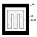
도6a는 본 발명의 제4실시형태에 따른 터치 입력 장치에 부착하기 위한 압력 전극을 포함하는 예시적인 전극 시트의 단면도이다. 예컨대, 전극 시트(440)는 제1절연층(470)과 제2절연층(471) 사이에 전극층(441)을 포함할 수 있다. 전극층(441)은 제1전극(450) 및/또는 제2전극(460)을 포함할 수 있다. 이때, 제1절연층(470)과 제2절연층(471)은 폴리이미드(polyimide)와 같은 절연 물질일 수 있다. 전극층(441)에 포함된 제1전극(450)과 제2전극(460)은 구리(copper)와 같은 물질을 포함할 수 있다. 전극 시트(440)의 제조 공정에 따라 전극층(441)과 제2절연층(471) 사이는 OCA(Optically Clear adhesive)와 같은 접착제(미도시)로 접착될 수 있다. 또한, 실시예에 따라 압력 전극(450, 460)은, 제1절연층(470) 위에 압력 전극 패턴에 상응하는 관통 구멍을 갖는 마스크(mask)를 위치시킨 후 전도성 스프레이(spray)를 분사함으로써 형성될 수 있다. 도6b 및 이하의 설명에서는 전극 시트(440)가 절연층(470, 471) 사이에 압력 전극(450, 460)을 포함하는 구조를 갖는 것으로 예시되나, 이는 단지 예시일 뿐이며 전극 시트(440)는 단순히 압력 전극(450, 460)만을 포함할 수도 있다.6A is a cross-sectional view of an exemplary electrode sheet including a pressure electrode for attaching to a touch input device according to a fourth embodiment of the present invention. For example, the
본 발명의 제4실시형태에 따른 터치 입력 장치(1000)에서 터치 압력을 검출할 수 있도록, 전극 시트(440)는 기판(300) 또는 디스플레이 모듈(200)과 스페이서층(420)을 사이에 두고 이격되도록 기판(300) 또는 디스플레이 모듈(200)에 부착될 수 있다.The
도6c는 제1방법에 따라 전극 시트(440)가 터치 입력 장치에 부착된 터치 입력 장치의 일부의 단면도이다. 도6c에서는 전극 시트(440)가 기판(300) 또는 디스플레이 모듈(200) 상에 부착된 것이 도시된다.6C is a cross-sectional view of a portion of the touch input device in which the
도6d에 도시된 바와 같이, 스페이서층(420)을 유지하기 위해서 전극 시트(440)의 테두리를 따라 소정 두께를 갖는 접착 테이프(430)가 형성될 수 있다. 도6d에서 접착 테이프(430)는 전극 시트(440)의 모든 테두리(예컨대, 4각형의 4면)에 형성된 것이 도시되나, 접착 테이프(430)는 전극 시트(440)의 테두리 중 적어도 일부(예컨대, 4각형의 3면)에만 형성될 수도 있다. 이때, 도6d에 도시된 바와 같이, 접착 테이프(430)는 전극 패턴(450, 460)을 포함하는 영역에는 형성되지 않을 수 있다. 이에 따라, 전극 시트(440)가 접착 테이프(430)를 통해 기판(300) 또는 디스플레이 모듈(200)에 부착될 때 압력 전극(450, 460)이 기판(300) 또는 디스플레이 모듈(200)과 소정 거리 이격되어 있을 수 있다. 실시예에 따라, 접착 테이프(430)는 기판(300)의 상부면 또는 디스플레이 모듈(200)의 하부면에 형성될 수 있다. 또한, 접착 테이프(440)는 양면 접착 테이프일 수 있다. 도6d에서는 압력 전극(450, 460) 중 하나의 압력 전극만을 예시하고 있다.An
도6e는 제2방법에 따라 전극 시트가 터치 입력 장치에 부착된 터치 입력 장치의 일부의 단면도이다. 도6e에서는 전극 시트(440)를 기판(300) 또는 디스플레이 모듈(200) 상에 위치시킨 후 접착 테이프(431)로 전극 시트(440)를 기판(300) 또는 디스플레이 모듈(200)에 고정시킬 수 있다. 이를 위해 접착 테이프(431)는 전극 시트(440)의 적어도 일부와 기판(300) 또는 디스플레이 모듈(200)의 적어도 일부에 접촉할 수 있다. 도6e에서는 접착 테이프(431)가 전극 시트(440)의 상부로부터 이어져 기판(300) 또는 디스플레이 모듈(200)의 노출 표면까지 이어지도록 도시된다. 이때, 접착 테이프(431)는 전극 시트(440)와 맞닿는 면 측에만 접착력이 있을 수 있다. 따라서, 도6e에서 접착 테이프(431)의 상부면은 접착력이 없을 수 있다.6E is a cross-sectional view of a portion of a touch input device in which an electrode sheet is attached to a touch input device according to a second method. 6E, the
도6e에 도시된 바와 같이, 전극 시트(440)를 접착 테이프(431)를 통해 기판(300) 또는 디스플레이 모듈(200)에 고정시키더라도 전극 시트(440)와 기판(300) 또는 디스플레이 모듈(200) 사이에는 소정의 공간, 즉 에어갭(420)이 존재할 수 있다. 이는 전극 시트(440)와 기판(300) 또는 디스플레이 모듈(200) 사이가 직접 접착제로 부착된 것이 아니며 또한 전극 시트(440)는 패턴을 갖는 전극(450, 460)을 포함하므로 전극 시트(440)의 표면은 편평하지 않을 수 있기 때문이다. 도6e에서의 에어갭(420) 또한 터치 압력을 검출하기 위한 스페이서층(420)으로서 기능할 수 있다.6E, even if the
이하에서는 도6c에 도시된 바와 같은 제1방법에 따라 전극 시트(440)가 기판(300) 또는 디스플레이 모듈(200)에 부착된 경우를 예로 하여 본 발명의 제4실시형태를 설명하나, 동일한 설명은 제2방법 등 임의의 방법에 따라 기판(300) 또는 디스플레이 모듈(200)과 이격되어 전극 시트(440)가 부착되는 경우에도 적용될 수 있다.Hereinafter, a fourth embodiment of the present invention will be described by taking the case where the
도6f는 본 발명의 제4실시예에 따른 압력 전극 패턴을 포함하는 터치 입력 장치의 단면도이다. 도6f에 도시된 바와 같이, 압력 전극(450, 460)을 포함하는 전극 시트(440)는 특히 압력 전극(450, 460)이 형성된 영역에서 기판(300)과 스페이서층(420)으로 이격되면서 기판(300)에 부착될 수 있다. 도6f에서 디스플레이 모듈(200)이 전극 시트(440)와 접촉되도록 도시되나 이는 단지 예시일 뿐이며 디스플레이 모듈(200)은 전극 시트(440)와 이격되어 위치할 수도 있다.6F is a cross-sectional view of a touch input device including a pressure electrode pattern according to a fourth embodiment of the present invention. The
도6g는 도6f에 도시된 터치 입력 장치(1000)에 압력이 인가된 경우의 단면도이다. 기판(300)은 노이즈 차폐를 위해 그라운드(ground) 전위를 가질 수 있다. 객체(500)를 통해 터치 센서 패널(100)의 표면에 압력을 인가하는 경우 터치 센서 패널(100) 및 디스플레이 모듈(200)은 휘어지거나 눌릴 수 있다. 이에 따라 전극 시트(440)가 눌려 전극 시트(440)에 포함된 압력 전극(450, 460)과 기판(300) 사이의 거리(d)가 d'로 감소할 수 있다. 이러한 경우, 상기 거리(d)의 감소에 따라 기판(300)으로 프린징 정전용량이 흡수되므로 제1전극(450)과 제2전극(460) 사이의 상호 정전용량은 감소할 수 있다. 따라서, 수신전극을 통해 획득되는 감지신호에서 상호 정전용량의 감소량을 획득하여 터치 압력의 크기를 산출할 수 있다.6G is a sectional view when pressure is applied to the
도6f 및 도6g에 도시된 바와 같이, 본 발명의 제4실시형태에 따른 터치 입력 장치(1000)는 전극 시트(440)가 부착된 기판(300)과 전극 시트(440) 사이의 거리 변화에 따라 터치 압력을 검출할 수 있다. 이때, 전극 시트(440)와 기판(300) 사이의 거리(d)는 매우 작으므로, 터치 압력에 따른 거리(d)의 미세한 변화에도 터치 압력을 정밀하게 검출할 수 있다.6F and 6G, the
도6h는 압력 전극(450, 460)이 디스플레이 모듈(200)의 하부면에 부착되는 것을 예시한다. 도6i는 도6h에 도시된 터치 입력 장치에 압력이 인가된 경우의 단면도이다. 이때, 디스플레이 모듈(300)은 그라운드 전위를 가질 수 있다. 따라서, 터치 센서 패널(100)의 터치 표면을 터치함에 따라 디스플레이 모듈(200)과 압력 전극(450, 460) 사이의 거리(d)가 감소하고, 결과적으로 제1전극(450)과 제2전극(460) 사이의 상호 정전용량의 변화를 야기할 수 있다.6H illustrates that the
도6h 및 도6i에 도시된 바와 같이, 본 발명의 제4실시형태에 따른 터치 입력 장치(1000)는 전극 시트(440)가 부착된 디스플레이 모듈(200)과 전극 시트(440) 사이의 거리 변화에 따라 터치 압력을 검출할 수도 있음을 알 수 있다.6H and 6I, the
예컨대, 실시예에 따라 전극 시트(440)와 기판(300) 사이의 거리에 비해 디스플레이 모듈(200)과 전극 시트(440) 사이의 거리는 더 작을 수 있다. 또한, 예컨대 전극 시트(440)와 그라운드 전위인 디스플레이 모듈(200)의 하부면 사이의 거리는, 전극 시트(440)와 디스플레이 모듈(200) 내에 위치하는 Vcom 전위층 및/또는 임의의 그라운드 전위 층과의 거리보다 작을 수 있다. 예컨대, 도2a 내지 도2c에 도시된 디스플레이 패널(200)에서 제1편광층(271)과 제1글라스층(261) 사이에 노이즈(noise) 차폐를 위한 전극(미도시)을 포함할 수 있으며 이러한 차폐를 위한 전극은 ITO로 구성될 수 있으며 그라운드 전위층 역할을 수행할 수 있다.For example, according to an embodiment, the distance between the
도6f 내지 도6i에 포함된 제1전극(450) 및 제2전극(460)는 도7a 내지 도7c에 예시된 패턴을 가질 수 있으며 상세한 설명은 중복되므로 생략한다.The
도6a 내지 도6i에서, 제1전극(450)과 제2전극(460)은 동일한 층에 형성된 것으로 도시되나, 제1전극(450)과 제2전극(460)은 실시예에 따라 서로 다른 층으로 구현될 수 있다. 도9b에 예시된 바와 같이, 전극 시트(440)에서 제1전극(450)은 제1절연층(470) 상에 형성되고 제2전극(460)은 제1전극(450) 상에 위치하는 제2절연층(471) 상에 형성되며, 제2전극(460)은 제3절연층(472)으로 덮일 수 있다.6A-6I, the
또한, 실시예에 따라 압력 전극(450, 460)이 제1전극(450)과 제2전극(460) 중 어느 하나의 압력 전극만을 포함하도록 구성될 수 있으며, 이러한 경우 하나의 압력 전극과 그라운드층(디스플레이 모듈(200) 또는 기판(300)) 사이의 정전용량 변화를 검출함으로써 터치 압력의 크기를 검출할 수도 있다. 이때, 압력 전극은 도7d에 예시된 바와 같이 판(예컨대, 사각판) 형상을 가질 수 있다. 이때, 도9c에 예시된 바와 같이, 전극 시트(440)에서 제1전극(450)은 제1절연층(470) 상에 형성되고 제2절연층(471)으로 덮일 수 있다.Also, according to the embodiment, the
도8a 및 도8b는 본 발명에 따른 터치 입력 장치에서 터치 압력의 크기와 포화 면적 사이의 관계를 나타낸다. 도8a 및 도8b에서는 전극 시트(440)가 기판(300)에 부착된 경우가 도시되나, 이하의 설명은 전극 시트(440)가 디스플레이 모듈(200)에 부착된 경우에도 동일하게 적용될 수 있다.8A and 8B show the relationship between the magnitude of the touch pressure and the saturated area in the touch input device according to the present invention. 8A and 8B illustrate a case where the
터치 압력의 크기가 충분히 큰 경우 소정 위치에서 전극 시트(440)와 기판(300) 사이의 거리가 더 이상 가까워지지 않는 상태에 다다를 수 있다. 이러한 상태를 이하에서는 포화 상태라고 지칭한다. 예컨대, 도8a에 예시된 바와 같이 힘(f)으로 터치 입력 장치(1000)를 누를 때 전극 시트(440)와 기판(300)은 접하여 더 이상 거리가 가까워질 수 없다. 이때, 도8a의 우측에서 전극 시트(440)와 기판(300)이 접촉하는 면적은 a로 표시될 수 있다.When the magnitude of the touch pressure is sufficiently large, the distance between the
하지만, 이러한 경우에도 터치 압력의 크기가 더 커지는 때에는 기판(300)과 전극 시트(440) 사이의 거리가 더 이상 가까워지지 않는 포화 상태에 있는 면적이 커질 수 있다. 예컨대, 도8b에 예시된 바와 같이 f보다 더 큰 힘(F)으로 터치 입력 장치(1000)를 누르면 전극 시트(440)와 기판(300)이 접촉하는 면적이 더 커질 수 있다. 도8b의 우측에서 전극 시트(440)와 기판(300)이 접촉하는 면적은 A로 표시될 수 있다. 이러한 면적이 커질수록 제1전극(450)과 제2전극(460) 사이의 상호 정전용량은 감소할 수 있다. 이하에서 거리의 변화에 따른 정전용량 변화에 따라서 터치 압력의 크기를 산출하는 것이 설명되나 이는 포화 상태에 있는 포화 면적의 변화에 따라서 터치 압력의 크기를 산출하는 것을 포함할 수 있다.However, even in such a case, when the magnitude of the touch pressure becomes larger, the area in the saturated state where the distance between the
도8a 및 도8b는 제4실시형태를 참조하여 설명되나, 도8a 및 도8b를 참조한 설명은 제1실시형태 내지 제3실시형태 및 아래서 설명하는 제5실시형태에도 동일하게 적용될 수 있음은 자명하다. 보다 구체적으로, 압력 전극(450, 460)과 그라운드층 또는 기준전위층(200, 300, 270) 사이의 거리가 더 이상 가까워질 수 없는 포화 상태에 있는 포화 면적의 변화에 따라서 터치 압력의 크기를 산출할 수 있다.
8A and 8B will be described with reference to the fourth embodiment. The description with reference to FIGS. 8A and 8B is applicable to the first to third embodiments and the fifth embodiment described below. Do. More specifically, the magnitude of the touch pressure in accordance with the change in the saturated area in which the distance between the
도10a 및 도10b는 본 발명의 제5실시형태에 따른 터치 입력 장치를 예시한다. 본 발명의 제5실시형태에 따른 터치 입력 장치(1000)는 터치 입력 장치의 상부 면뿐 아니라 하부 면에 압력을 인가하는 경우에도 터치 압력을 감지할 수 있다. 본 명세서에서 터치 표면으로서 터치 입력 장치(100)의 상부 면은 디스플레이 모듈(200)의 상부 면으로 지칭될 수 있으며 이는 디스플레이 모듈(200)의 상부 표면뿐 아니라 디스플레이 모듈(200)을 도면의 상측에서 덮고 있는 표면을 포함할 수 있다. 또한, 본 명세서에서 터치 표면으로서 터치 입력 장치(100)의 하부면은 기판(300)의 하부 면으로 지칭될 수 있으며 이는 기판(300)의 하부 표면뿐 아니라 도면의 하측에서 기판(300)을 덮고 있는 표면을 포함할 수 있다.10A and 10B illustrate a touch input device according to a fifth embodiment of the present invention. The
도10a에서는 제2실시형태에서 압력 전극(450, 460)이 디스플레이 모듈(200)의 하부면상에 위치하는 경우로서, 기판(300)의 하부면에 압력을 인가하여 기판(300)이 눌리거나 휘어짐을 통해서 기판(300)과 압력 전극(450, 460) 사이의 거리가 변화하는 경우를 예시한다. 이때, 기준전위층인 기판(300) 과의 거리가 변화함에 따라 제1전극(450)과 제2전극(460) 사이의 정전용량 또는 제1전극(450)(또는 제2전극(460)과 기판(300) 사이의 정전용량이 변화하므로 터치 압력을 검출할 수 있다.10A shows a case where the
도10b에서는 제3실시형태에서 전극 시트(440)가 기판(300)에 부착된 경우로서, 기판(300)의 하부면에 압력을 인가하여 기판(300)이 눌리거나 휘어짐을 통해서 기판(300)과 전극 시트(440) 사이의 거리가 변화하는 경우를 예시한다. 도10a의 경우와 마찬가지로, 기준전위층인 기판(300) 과의 거리가 변화함에 따라 제1전극(450)과 제2전극(460) 사이의 정전용량 또는 제1전극(450)(또는 제2전극(460)과 기판(300) 사이의 정전용량이 변화하므로 터치 압력을 검출할 수 있다.10B shows a case where the
도10a 및 도10b에서 제2실시형태 및 제3실시형태의 일부 예에 대해서 제5실시형태를 설명하였으나, 제5실시형태는 제1실시형태 내지 제4실시형태로서 기판(300)의 하부 면에 압력을 인가하여 기판(300)이 휘어지거나 눌림으로 인해 제1전극(450)과 제2전극(460) 사이의 정전용량, 또는 제1전극(450)과 기준전위층(200, 300, 270) 사이의 정전용량이 변화하는 경우에 모두 적용될 수 있다. 예컨대, 도4c에 도시된 바와 같은 구조에서 기판(300)이 휘어지거나 눌림을 통해서 압력 전극(450, 460)과 디스플레이 모듈(200) 사이의 거리가 변화할 수 있고, 이에 따라 압력 검출이 가능할 수 있다.
10A and 10B, the fifth embodiment has been described with respect to some examples of the second embodiment and the third embodiment. However, the fifth embodiment is a modification of the first embodiment through the fourth embodiment, The
이상에서 살펴본 바와 같이, 본 발명의 실시예에 따른 터치 입력 장치(1000)는 압력 전극(450, 460)에서 발생하는 정전용량의 변화를 감지한다. 따라서, 제1전극(450)과 제2전극(460) 중 구동전극에는 구동신호가 인가될 필요가 있고 수신전극으로부터 감지신호를 획득하여 정전용량의 변화량으로부터 터치 압력을 산출해야 한다. 실시예에 따라, 압력 검출의 동작을 위한 터치 센싱 IC를 추가로 포함하는 것도 가능하다. 이러한 경우, 도1에 예시된 바와 같이, 구동부(120), 감지부(110) 및 제어부(130)와 유사한 구성을 중복하여 포함하게 되므로 터치 입력 장치(1000)의 면적 및 부피가 커지는 문제점이 발생할 수 있다.As described above, the
실시예에 따라, 터치 입력 장치(1000)는 압력 검출을 위해 터치 센서 패널(100)의 작동을 위한 터치 검출 장치를 통해 구동신호가 인가되고 감지신호를 입력받아 터치 압력을 검출할 수 있다. 이하에서는, 제1전극(450)이 구동전극이고 제2전극(460)이 수신전극인 경우를 가정하여 설명한다.The
이를 위해, 본 발명의 실시예에 따른 터치 입력 장치(1000)에서 제1전극(450)은 구동부(120)로부터 구동신호를 인가받고 제2전극(460)은 감지신호를 감지부(110)에 전달할 수 있다. 제어부(130)는 터치 센서 패널(100)의 스캐닝을 수행함과 동시에 압력 검출의 스캐닝을 수행하도록 하거나, 또는 제어부(130)는 시분할하여 제1시간구간에는 터치 센서 패널(100)의 스캐닝을 수행하도록 하고 제1시간구간과는 다른 제2시간구간에는 압력 검출의 스캐닝을 수행하도록 제어신호를 생성할 수 있다.The
따라서, 본 발명의 실시예에서 제1전극(450)과 제2전극(460)는 전기적으로 구동부(120) 및/또는 감지부(110)에 연결되어야 한다. 이때, 터치 센서 패널(100)을 위한 터치 검출 장치는 터치 센싱 IC(150)로서 터치 센서 패널(100)의 일단 또는 터치 센서 패널(100)와 동일 평면상에 형성되는 것이 일반적이다. 압력 전극 패턴(450, 460)은 임의의 방법으로 터치 센서 패널(100)의 터치 검출 장치와 전기적으로 연결될 수 있다. 예컨대, 압력 전극 패턴(450, 460)은 디스플레이 모듈(200)에 포함된 제2PCB(210)를 이용하여 커넥터(connector)를 통해 터치 검출 장치에 연결될 수 있다. 예컨대, 도4b 및 도5c에 도시된 바와 같이 제1전극(450)과 제2전극(460)으로부터 각각 전기적으로 연장되는 전도성 트레이스들(460)은 제2PCB(210) 등을 통하여 터치 센싱 IC(150)까지 전기적으로 연결될 수 있다.Therefore, in the embodiment of the present invention, the
도11a 및 도11b는 압력 전극(450, 460, 또는 전극 시트(440))이 디스플레이 모듈(200)의 하부면에 부착되는 경우를 나타낸다. 도11a 및 도11b에서 디스플레이 모듈(200)은 하부면 일부에 디스플레이 패널의 작동을 위한 회로가 실장된 제2PCB(210)가 도시된다.11A and 11B show the case where the
도11a는 제1전극(450)과 제2전극(460)이 디스플레이 모듈(200)의 제2PCB(210)의 일단에 연결되도록 압력 전극(450, 460)을 디스플레이 모듈(200)의 하부면에 부착하는 경우를 예시한다. 이때, 도11a에서는 제1전극(450)과 제2전극(460)이 절연층(470) 상에 제작된 경우를 예시한다. 압력 전극(450, 460)은 절연층(470) 상에 형성되어 일체형 시트(sheet)로서 디스플레이 모듈(200)의 하부면에 부착될 수도 있다. 제2PCB(210) 상에는 압력 전극(450, 460)을 터치 센싱 IC(150) 등 필요한 구성까지 전기적으로 연결할 수 있도록 도전성 패턴이 인쇄되어 있을 수 있다. 이에 대한 상세한 설명은 도12a 내지 도12c를 참조하여 설명한다. 도11a에 예시된 압력 전극(450, 460)의 부착 방법은 기판(300)에 대해서도 동일하게 적용될 수 있다.11A shows a state in which the
도11b는 제1전극(450)과 제2전극(460)이 디스플레이 모듈(200)의 제2PCB(210)에 일체형으로 형성된 경우를 예시한다. 예컨대, 디스플레이 모듈(200)의 제2PCB(210) 제작시에 제2PCB에 일정 면적(211)을 할애하여 미리 디스플레이 패널의 작동을 위한 회로뿐 아니라 제1전극(450)과 제2전극(460)에 해당하는 패턴까지 인쇄할 수 있다. 제2PCB(210)에는 제1전극(450) 및 제2전극(460)을 터치 센싱 IC(150) 등 필요한 구성까지 전기적으로 연결하는 도전성 패턴이 인쇄되어 있을 수 있다.11B illustrates a case where the
도12a 내지 도12c는 압력 전극(450, 460 또는 전극 시트(440))을 터치 센싱 IC(150)에 연결하는 방법을 예시한다. 도12a 내지 도12c에서 터치 센서 패널(100)이 디스플레이 모듈(200)의 외부에 포함된 경우로서, 터치 센서 패널(100)의 터치 검출 장치가 터치 센서 패널(100)을 위한 제1PCB(160)에 실장된 터치 센싱 IC(150)에 집적된 경우를 예시한다.12A to 12C illustrate a method of connecting the
도12a에서 디스플레이 모듈(200)에 부착된 압력 전극(450, 460)이 제1커넥터(121)를 통해 터치 센싱 IC(150)까지 연결되는 경우를 예시한다. 도10a에 예시된 바와 같이, 스마트폰과 같은 이동 통신 장치에서 터치 센싱 IC(150)는 제1커넥터(connector: 121)를 통해서 디스플레이 모듈(200)을 위한 제2PCB(210)에 연결된다. 제2PCB(210)는 제2커넥터(224)를 통해서 메인보드로 전기적으로 연결될 수 있다. 따라서, 터치 센싱 IC(150)는 제1커넥터(121) 및 제2커넥터(224)를 통해서 터치 입력 장치(1000)의 작동을 위한 CPU 또는 AP와 신호를 주고 받을 수 있다.12A illustrates a case where the
이때, 도12a에서는 압력 전극(450)이 도11b에 예시된 바와 같은 방식으로 디스플레이 모듈(200)에 부착된 것이 예시되나 도11a에 예시된 바와 같은 방식으로 부착된 경우에도 적용될 수 있다. 제2PCB(210)에는 압력 전극(450, 460)이 제1커넥터(121)를 통해 터치 센싱 IC(150)까지 전기적으로 연결될 수 있도록 도전성 패턴이 인쇄되어 있을 수 있다.Here, in FIG. 12A, the
도12b에서 디스플레이 모듈(200)에 부착된 압력 전극(450, 460)이 제3커넥터(471)를 통해서 터치 센싱 IC(150)까지 연결되는 경우가 예시된다. 도12b에서 압력 전극(450, 460)은 제3커넥터(471)를 통해서 터치 입력 장치(1000)의 작동을 위한 메인보드까지 연결되고, 추후 제2커넥터(224) 및 제1커넥터(121)를 통해서 터치 센싱 IC(150)까지 연결될 수 있다. 이때, 압력 전극(450, 460)은 제2PCB(210)와 분리된 추가의 PCB(211) 상에 인쇄될 수 있다. 또는 실시예에 따라 압력 전극(450, 460)은 절연층(470) 상에 형성되고 압력 전극(450, 460)으로부터 전도성 트레이스등을 연장시켜 커넥터(471)를 통해 메인보드까지 연결될 수도 있다.The case where the
도12c에서 압력 전극(450, 460)이 제4커넥터(472)를 통해서 직접 터치 센싱 IC(150)로 연결되는 경우가 예시된다. 도12c에서 압력 전극(450, 460)은 제4커넥터(472)를 통해 제1PCB(160)까지 연결될 수 있다. 제1PCB(160)에는 제4커넥터(472)부터 터치 센싱 IC(150)까지 전기적으로 연결하는 도전성 패턴이 인쇄되어 있을 수 있다. 이에 따라, 압력 전극(450, 460)은 제4커넥터(472)를 통해서 터치 센싱 IC(150)까지 연결될 수 있다. 이때, 압력 전극(450, 460)은 제2PCB(210)와 분리된 추가의 PCB(211) 상에 인쇄될 수 있다. 제2PCB(472)와 추가의 PCB(211)는 서로 단락되지 않도록 절연되어 있을 수 있다. 또는 실시예에 따라 압력 전극(450, 460)은 절연층(470) 상에 형성되고 압력 전극(450, 460)으로부터 전도성 트레이스등을 연장시켜 커넥터(472)를 통해 제1PCB(160)까지 연결될 수도 있다.The case where the
도12b 및 도12c의 연결 방법은 압력 전극(450, 460)이 디스플레이 모듈(200)의 하부면뿐 아니라 기판(300)상에 형성된 경우에도 적용될 수 있다.12B and 12C can be applied to the case where the
도12a 내지 도12c에서는 터치 센싱 IC(150)가 제1PCB(160) 상에 형성된 COF(chip on film) 구조를 가정하여 설명되었다. 하지만, 이는 단지 예시일 뿐이며 본 발명은 터치 센싱 IC(150)가 터치 입력 장치(1000)의 실장공간(310) 내의 메인보드 상에 실장되는 COB(chip on board) 구조의 경우에도 적용될 수 있다. 도12a 내지 도12c에 대한 설명으로부터 당해 기술분야의 당업자에게 다른 실시예의 경우에 압력 전극(450, 460)의 커넥터를 통한 연결이 자명할 것이다.12A to 12C, the
이상에서는 구동전극으로서 제1전극(450)이 하나의 채널을 구성하고 수신전극으로서 제2전극(460)이 하나의 채널을 구성하는 압력 전극(450, 460)에 대해서 살펴보았다. 하지만, 이는 단지 예시일 뿐이며, 실시예에 따라 구동전극 및 수신전극은 각각 복수개의 채널을 구성하여 다중터치(multi touch)에 따라 다중의 압력 검출이 가능할 수 있다.In the above description, the
도13a 내지 도13c는 본 발명의 압력 전극이 복수의 채널을 구성하는 경우를 예시한다. 도13a에서는 제1전극(450-1, 450-2)과 제2전극(460-1, 460-2) 각각이 2개의 채널을 구성하는 경우가 예시된다. 도13b에서는 제1전극(450)은 2개의 채널(450-1, 450-2)을 구성하나 제2전극(460)은 1개의 채널을 구성하는 경우가 예시된다. 도13c에서는 제1전극(450-1 내지 450-5)과 제2전극(460-1, 460-5) 각각이 5개의 채널을 구성하는 경우가 예시된다.13A to 13C illustrate a case where the pressure electrode of the present invention constitutes a plurality of channels. 13A illustrates a case where the first electrodes 450-1 and 450-2 and the second electrodes 460-1 and 460-2 constitute two channels. 13B illustrates a case where the
도13a 내지 도13c는 압력 전극이 단수 또는 복수의 채널을 구성하는 경우를 예시하며 다양한 방법으로 압력 전극이 단수 또는 복수의 채널로 구성될 수 있다. 도13a 내지 도13c에서 압력 전극(450, 460)이 터치 센싱 IC(150)에 전기적으로 연결되는 경우가 예시되지 않았으나, 도12a 내지 도12c 및 기타의 방법으로 압력 전극(450, 460)이 터치 센싱 IC(150)에 연결될 수 있다.13A to 13C illustrate the case where the pressure electrode constitutes a single channel or a plurality of channels, and the pressure electrode may be composed of a single channel or a plurality of channels in various ways. 13A to 13C illustrate a case where the
도14는 본 발명의 실시형태에 따른 터치 입력 장치(1000)의 터치 표면 중심부를 비전도성 객체로 가압하는 실험을 수행하여, 객체의 그램중량(gram force)에 따른 정전용량의 변화량을 표시하는 그래프이다. 도14에서 알 수 있는 바와 같이, 본 발명의 실시예에 따른 터치 입력 장치(1000)의 터치 표면 중심부를 가압하는 힘이 커질수록 압력 검출을 위한 압력 전극 패턴(450, 460)의 정전용량의 변화량이 커짐을 알 수 있다.14 is a graph showing a change in capacitance according to a gram force of an object by performing an experiment for pressing the center of the touch surface of the
이상에서는 압력 검출을 위해 정전용량 방식의 검출 모듈이 설명되었으나, 본 발명의 실시예에 따른 터치 입력 장치(1000)는 압력 검출을 위해 스페이서층(420, 220) 및 압력 전극(450, 460 또는 전극 시트(440))을 이용하는 경우라면 임의의 방식의 압력 검출 모듈을 이용할 수 있다.The
또한, 이상에서 실시예를 중심으로 설명하였으나 이는 단지 예시일 뿐 본 발명을 한정하는 것이 아니며, 본 발명이 속하는 분야의 통상의 지식을 가진 자라면 본 실시예의 본질적인 특성을 벗어나지 않는 범위에서 이상에 예시되지 않은 여러 가지의 변형과 응용이 가능함을 알 수 있을 것이다. 예를 들어, 실시예에 구체적으로 나타난 각 구성 요소는 변형하여 실시할 수 있는 것이다. 그리고 이러한 변형과 응용에 관계된 차이점들은 첨부된 청구 범위에서 규정하는 본 발명의 범위에 포함되는 것으로 해석되어야 할 것이다.While the present invention has been particularly shown and described with reference to exemplary embodiments thereof, it is clearly understood that the same is by way of illustration and example only and is not to be taken by way of illustration, It can be seen that various modifications and applications are possible. For example, each component specifically shown in the embodiments can be modified and implemented. It is to be understood that all changes and modifications that come within the meaning and range of equivalency of the claims are therefore intended to be embraced therein.
1000: 터치 입력 장치 100: 터치 센서 패널
120: 구동부 110: 감지부
130: 제어부 200: 디스플레이 모듈
300: 기판 400: 압력 검출 모듈
420; 스페이서층 전극시트: 440
450, 460: 전극1000: touch input device 100: touch sensor panel
120: driving unit 110:
130: control unit 200: display module
300: substrate 400: pressure detection module
420; Spacer layer Electrode sheet: 440
450, 460: electrode
Claims (16)
Translated fromKorean기판; 및
디스플레이 모듈;을 포함하고,
상기 터치 표면에 대한 상기 터치에 따라 기준 전위층과의 거리가 변할 수 있는 위치에 배치된 전극을 더 포함하며,
상기 거리는 상기 터치의 압력 크기에 따라 달라질 수 있으며,
상기 전극은 상기 거리의 변화에 따른 전기적 신호를 출력할 수 있고,
상기 기준 전위층과 상기 전극 사이에 스페이서층이 위치하는,
터치 입력 장치.A touch input device capable of detecting pressure of a touch on a touch surface,
Board; And
And a display module,
And an electrode disposed at a position where a distance from the reference potential layer can be changed according to the touch with respect to the touch surface,
The distance may vary depending on the pressure magnitude of the touch,
The electrode can output an electrical signal according to the change of the distance,
Wherein a spacer layer is located between the reference potential layer and the electrode,
Touch input device.
상기 전극은 상기 기판 또는 상기 디스플레이 모듈상에 형성되며,
상기 거리에 따라 상기 전극과 상기 기준 전위층 사이의 정전용량이 변화하는, 터치 입력 장치.The method according to claim 1,
The electrode being formed on the substrate or the display module,
And a capacitance between the electrode and the reference potential layer changes according to the distance.
상기 전극은 제1절연층과 제2절연층 사이에 위치하여, 일체형의 전극 시트로 상기 제1절연층 및 상기 제2절연층과 함께 상기 기판 또는 상기 디스플레이 모듈에 고정되며,
상기 전극이 고정되는 상기 기판 또는 상기 디스플레이 모듈이 상기 기준 전위층인, 터치 입력 장치.3. The method of claim 2,
Wherein the electrode is positioned between the first insulating layer and the second insulating layer and is fixed to the substrate or the display module together with the first insulating layer and the second insulating layer by an integral electrode sheet,
Wherein the substrate on which the electrode is fixed or the display module is the reference potential layer.
상기 기준 전위층은 상기 기판 또는 상기 디스플레이 모듈이거나 상기 디스플레이 모듈 내부에 위치하는, 터치 입력 장치.3. The method of claim 2,
Wherein the reference potential layer is either the substrate or the display module or is located inside the display module.
상기 전극은 제1전극과 제2전극을 포함하며, 상기 거리에 따라 상기 제1전극과 상기 제2전극 사이의 정전용량이 변화하며,
상기 기준 전위층은 상기 기판 또는 상기 디스플레이 모듈이거나 상기 디스플레이 모듈 내부에 위치하는, 터치 입력 장치.The method according to claim 1,
Wherein the electrode comprises a first electrode and a second electrode, the capacitance between the first electrode and the second electrode varying with the distance,
Wherein the reference potential layer is either the substrate or the display module or is located inside the display module.
상기 제1전극 및 상기 제2전극이 상기 기판상에 형성되거나, 상기 제1전극 및 상기 제2전극이 상기 디스플레이 모듈상에 형성되거나, 또는 상기 제1전극과 상기 제2전극 중 어느 하나는 상기 기판상에 형성되고 나머지 하나는 상기 디스플레이 모듈상에 형성되는, 터치 입력 장치.6. The method of claim 5,
Wherein the first electrode and the second electrode are formed on the substrate, or the first electrode and the second electrode are formed on the display module, or one of the first electrode and the second electrode is formed on the substrate, And the other is formed on the display module.
상기 전극은 제1절연층과 제2절연층 사이에 위치하여, 일체형의 전극 시트로 상기 제1절연층 및 상기 제2절연층과 함께 상기 기판 또는 상기 디스플레이 모듈에 고정되며,
상기 전극이 고정되는 상기 기판 또는 상기 디스플레이 모듈이 상기 기준 전위층이고,
상기 전극은 제1전극과 제2전극을 포함하며, 상기 거리에 따라 상기 제1전극과 상기 제2전극 사이의 정전용량이 변화하는, 터치 입력 장치.The method according to claim 1,
Wherein the electrode is positioned between the first insulating layer and the second insulating layer and is fixed to the substrate or the display module together with the first insulating layer and the second insulating layer by an integral electrode sheet,
The substrate on which the electrode is fixed or the display module is the reference potential layer,
Wherein the electrode includes a first electrode and a second electrode, and the electrostatic capacitance between the first electrode and the second electrode changes according to the distance.
상기 전극은 상기 전극 패턴에 상응하는 관통구멍을 갖는 마스크(mask)를 위치시킨 후, 전도성 스프레이를 분사함으로써 형성되는, 터치 입력 장치.8. The method according to any one of claims 1 to 7,
Wherein the electrode is formed by positioning a mask having a through hole corresponding to the electrode pattern, and then spraying a conductive spray.
상기 터치 표면에 대한 상기 터치에 따라 상기 디스플레이 모듈이 적어도 상기 터치의 위치에서 휘어지는, 터치 입력 장치.8. The method according to any one of claims 1 to 7,
Wherein the display module is bent at least in the position of the touch according to the touch on the touch surface.
상기 터치 표면은 상기 디스플레이 모듈의 상부표면 및 상기 기판의 하부면 중 적어도 하나 일 수 있는, 터치 입력 장치.8. The method according to any one of claims 1 to 7,
Wherein the touch surface can be at least one of an upper surface of the display module and a lower surface of the substrate.
상기 터치 표면에 대한 상기 터치시 상기 터치의 위치를 검출할 수 있도록 하는 터치 센서 패널; 및
상기 터치 센서 패널의 작동을 위한 터치 센싱 회로를 실장한 제1인쇄 회로 기판을 더 포함하며,
상기 터치 센서 패널은, 상기 디스플레이 모듈 상에 있어서 상기 기판과 반대측 면상에 접착되는, 터치 입력 장치.8. The method according to any one of claims 1 to 7,
A touch sensor panel for detecting a position of the touch when touching the touch surface; And
And a first printed circuit board on which a touch sensing circuit for operating the touch sensor panel is mounted,
Wherein the touch sensor panel is adhered on the surface opposite to the substrate on the display module.
상기 디스플레이 모듈은 상기 디스플레이 패널의 작동을 위한 제어 회로를 실장한 제2인쇄 회로 기판을 더 포함하고,
상기 전극은 상기 제2인쇄 회로 기판상에 인쇄되어 있는, 터치 입력 장치The method according to claim 1,
Wherein the display module further includes a second printed circuit board on which a control circuit for operating the display panel is mounted,
Wherein the electrode is printed on the second printed circuit board,
상기 디스플레이 모듈은 상기 디스플레이 패널의 작동을 위한 제어 회로를 실장한 제2인쇄 회로 기판을 더 포함하며,
상기 전극은 상기 제2인쇄 회로 기판에 인쇄된 전도성 패턴과 전기적으로 연결되도록 상기 디스플레이 모듈상에 부착되는, 터치 입력 장치.The method according to claim 1,
The display module further includes a second printed circuit board on which a control circuit for operating the display panel is mounted,
Wherein the electrode is attached on the display module to be electrically connected to the conductive pattern printed on the second printed circuit board.
상기 터치 표면에 대한 상기 터치시 상기 터치의 위치를 검출할 수 있도록 하는 터치 센서 패널; 및
상기 터치 센서 패널의 작동을 위한 터치 센싱 회로를 실장한 제1인쇄 회로 기판을 더 포함하고,
상기 터치 센서 패널은, 상기 디스플레이 모듈 상에 있어서 상기 기판과 반대측 면상에 접착되고,
상기 제1인쇄 회로 기판과 상기 제2인쇄 회로 기판 사이에 커넥터를 더 포함하며,
상기 전극은 상기 커넥터를 통해 상기 터치 센싱 회로에 전기적으로 연결되는,
터치 입력 장치.The method according to claim 12 or 13,
A touch sensor panel for detecting a position of the touch when touching the touch surface; And
Further comprising a first printed circuit board on which a touch sensing circuit for operating the touch sensor panel is mounted,
Wherein the touch sensor panel is bonded on a surface of the display module opposite to the substrate,
Further comprising a connector between the first printed circuit board and the second printed circuit board,
The electrode being electrically connected to the touch sensing circuit through the connector,
Touch input device.
상기 디스플레이 모듈은 상기 디스플레이 패널의 작동을 위한 제어 회로를 실장한 제2인쇄 회로 기판을 더 포함하고,
상기 전극은 추가의 회로 기판에 형성되어 있고,
상기 추가의 회로 기판과 상기 제1인쇄 회로 기판 사이에 커넥터를 더 포함하며,
상기 전극은 상기 커넥터를 통해 상기 터치 센싱 회로에 전기적으로 연결되는, 터치 입력 장치.12. The method of claim 11,
Wherein the display module further includes a second printed circuit board on which a control circuit for operating the display panel is mounted,
The electrode is formed on an additional circuit board,
Further comprising a connector between said additional circuit board and said first printed circuit board,
And the electrode is electrically connected to the touch sensing circuit through the connector.
상기 디스플레이 모듈은 상기 디스플레이 패널의 작동을 위한 제어 회로를 실장한 제2인쇄 회로 기판을 더 포함하고,
상기 전극은 추가의 회로 기판에 형성되어 있고,
상기 제1인쇄 회로 기판과 상기 제2인쇄 회로 기판 사이에 제1커넥터; 상기 제2인쇄 회로 기판과 상기 터치 입력 장치의 작동을 위한 중앙 처리 유닛을 실장한 메인보드 사이에 제2커넥터; 및 상기 추가의 회로 기판과 상기 메인보드 사이에 제3커넥터를 더 포함하며,
상기 전극은 상기 제1커넥터, 상기 제2커넥터 및 상기 제3커넥터를 통해 상기 터치 센싱 회로에 전기적으로 연결되는, 터치 입력 장치.12. The method of claim 11,
Wherein the display module further includes a second printed circuit board on which a control circuit for operating the display panel is mounted,
The electrode is formed on an additional circuit board,
A first connector between the first printed circuit board and the second printed circuit board; A second connector between the second printed circuit board and the main board on which the central processing unit for operating the touch input device is mounted; And a third connector between the additional circuit board and the main board,
And the electrode is electrically connected to the touch sensing circuit through the first connector, the second connector, and the third connector.
Priority Applications (29)
| Application Number | Priority Date | Filing Date | Title |
|---|---|---|---|
| KR1020140186352AKR101693337B1 (en) | 2014-12-22 | 2014-12-22 | Touch input device |
| JP2015019094AJP6527343B2 (en) | 2014-08-01 | 2015-02-03 | Touch input device |
| US14/614,086US10474271B2 (en) | 2014-08-01 | 2015-02-04 | Touch input device |
| EP15154188.5AEP2980685B1 (en) | 2014-08-01 | 2015-02-06 | Touch input device |
| JP2015024602AJP6247651B2 (en) | 2014-03-24 | 2015-02-10 | Menu operation method and menu operation device including touch input device for performing the same |
| US14/618,750US20150268802A1 (en) | 2014-03-24 | 2015-02-10 | Menu control method and menu control device including touch input device performing the same |
| US14/623,781US20150268827A1 (en) | 2014-03-24 | 2015-02-17 | Method for controlling moving direction of display object and a terminal thereof |
| CN201510086606.6ACN105320346B (en) | 2014-08-01 | 2015-02-17 | Touch input device |
| CN201910173131.2ACN109901750B (en) | 2014-08-01 | 2015-02-17 | Touch input device |
| JP2015040046AJP6109218B2 (en) | 2014-03-24 | 2015-03-02 | Method of adjusting moving direction of display object and terminal |
| US14/663,551US10104270B2 (en) | 2014-03-24 | 2015-03-20 | Method for operating camera underwater |
| JP2015060026AJP2015185173A (en) | 2014-03-24 | 2015-03-23 | Temporary operation method of operation object by touch pressure and touch area and terminal |
| JP2015060025AJP6484079B2 (en) | 2014-03-24 | 2015-03-23 | Kansei transmission method and terminal for the same |
| JP2015060023AJP6326001B2 (en) | 2014-03-24 | 2015-03-23 | Underwater operation of the camera |
| US14/666,352US9971435B2 (en) | 2014-03-24 | 2015-03-24 | Method for transmitting emotion and terminal for the same |
| US14/666,471US10268322B2 (en) | 2014-03-24 | 2015-03-24 | Method for temporarily manipulating operation of object in accordance with touch pressure or touch area and terminal thereof |
| JP2016238164AJP2017079079A (en) | 2014-03-24 | 2016-12-08 | Menu operation method and menu operation device including touch input device conducting menu operation |
| JP2017042491AJP6577967B2 (en) | 2014-03-24 | 2017-03-07 | Method of adjusting moving direction of display object and terminal |
| JP2017093158AJP2017174447A (en) | 2014-03-24 | 2017-05-09 | Underwater camera operating method |
| JP2017212104AJP2018049646A (en) | 2014-03-24 | 2017-11-01 | Temporary operation method of operation object by touch pressure and touch area and terminal |
| JP2017212092AJP2018032435A (en) | 2014-03-24 | 2017-11-01 | Sensitivity transmission method and terminal therefor |
| JP2017226677AJP6706239B2 (en) | 2014-08-01 | 2017-11-27 | Touch input device |
| US16/121,438US10404898B2 (en) | 2014-03-24 | 2018-09-04 | Method for operating camera underwater |
| US16/660,754US10983648B2 (en) | 2014-08-01 | 2019-10-22 | Touch input device |
| JP2019232270AJP2020064651A (en) | 2014-03-24 | 2019-12-24 | Temporary operation method and terminal of operation target by touch pressure and touch area |
| US17/209,163US11301103B2 (en) | 2014-08-01 | 2021-03-22 | Touch input device |
| US17/704,988US11709573B2 (en) | 2014-08-01 | 2022-03-25 | Touch input device |
| US18/208,656US12086370B2 (en) | 2014-08-01 | 2023-06-12 | Touch input device |
| US18/827,475US20240427465A1 (en) | 2014-08-01 | 2024-09-06 | Touch input device |
Applications Claiming Priority (1)
| Application Number | Priority Date | Filing Date | Title |
|---|---|---|---|
| KR1020140186352AKR101693337B1 (en) | 2014-12-22 | 2014-12-22 | Touch input device |
Related Child Applications (1)
| Application Number | Title | Priority Date | Filing Date |
|---|---|---|---|
| KR1020160034887ADivisionKR20160076490A (en) | 2016-03-23 | 2016-03-23 | Touch input device |
Publications (2)
| Publication Number | Publication Date |
|---|---|
| KR20160076298Atrue KR20160076298A (en) | 2016-06-30 |
| KR101693337B1 KR101693337B1 (en) | 2017-01-06 |
Family
ID=56352768
Family Applications (1)
| Application Number | Title | Priority Date | Filing Date |
|---|---|---|---|
| KR1020140186352AActiveKR101693337B1 (en) | 2014-03-24 | 2014-12-22 | Touch input device |
Country Status (1)
| Country | Link |
|---|---|
| KR (1) | KR101693337B1 (en) |
Cited By (6)
| Publication number | Priority date | Publication date | Assignee | Title |
|---|---|---|---|---|
| WO2018026245A1 (en)* | 2016-08-05 | 2018-02-08 | Samsung Electronics Co., Ltd. | Electronic device including display equipped with force sensor |
| KR20180017636A (en)* | 2016-08-10 | 2018-02-21 | 주식회사 아모센스 | Sensor for detecting touch pressure |
| KR20180023379A (en)* | 2016-08-25 | 2018-03-07 | 주식회사 하이딥 | Touch input device |
| KR20180113219A (en)* | 2016-09-22 | 2018-10-15 | 애플 인크. | Display module and glass with undercut plastic frame |
| KR20190095006A (en)* | 2018-02-06 | 2019-08-14 | 주식회사 하이딥 | Touch input apparatus |
| US10631437B2 (en) | 2016-09-22 | 2020-04-21 | Apple Inc. | Display module and glass with undercut plastic frame |
Families Citing this family (1)
| Publication number | Priority date | Publication date | Assignee | Title |
|---|---|---|---|---|
| KR102802744B1 (en) | 2019-03-28 | 2025-05-02 | 삼성디스플레이 주식회사 | Display device |
Citations (4)
| Publication number | Priority date | Publication date | Assignee | Title |
|---|---|---|---|---|
| KR20120053716A (en)* | 2010-11-18 | 2012-05-29 | 신화인터텍 주식회사 | Method of manufacturing patterned transparent conductive film |
| WO2013132736A1 (en)* | 2012-03-09 | 2013-09-12 | ソニー株式会社 | Sensor device, input device, and electronic apparatus |
| KR20130131647A (en)* | 2012-05-24 | 2013-12-04 | (주)멜파스 | Touch screen panel including window having electrode formed therewith as one body, and touch screen display apparatus including thereof |
| JP2014194591A (en)* | 2013-03-28 | 2014-10-09 | Fujitsu Ltd | Detection device, detection method, and electronic apparatus |
- 2014
- 2014-12-22KRKR1020140186352Apatent/KR101693337B1/enactiveActive
Patent Citations (4)
| Publication number | Priority date | Publication date | Assignee | Title |
|---|---|---|---|---|
| KR20120053716A (en)* | 2010-11-18 | 2012-05-29 | 신화인터텍 주식회사 | Method of manufacturing patterned transparent conductive film |
| WO2013132736A1 (en)* | 2012-03-09 | 2013-09-12 | ソニー株式会社 | Sensor device, input device, and electronic apparatus |
| KR20130131647A (en)* | 2012-05-24 | 2013-12-04 | (주)멜파스 | Touch screen panel including window having electrode formed therewith as one body, and touch screen display apparatus including thereof |
| JP2014194591A (en)* | 2013-03-28 | 2014-10-09 | Fujitsu Ltd | Detection device, detection method, and electronic apparatus |
Cited By (11)
| Publication number | Priority date | Publication date | Assignee | Title |
|---|---|---|---|---|
| WO2018026245A1 (en)* | 2016-08-05 | 2018-02-08 | Samsung Electronics Co., Ltd. | Electronic device including display equipped with force sensor |
| US10531580B2 (en) | 2016-08-05 | 2020-01-07 | Samsung Electronics Co., Ltd. | Electronic device including display equipped with force sensor |
| KR20180017636A (en)* | 2016-08-10 | 2018-02-21 | 주식회사 아모센스 | Sensor for detecting touch pressure |
| KR20180023379A (en)* | 2016-08-25 | 2018-03-07 | 주식회사 하이딥 | Touch input device |
| KR20180113219A (en)* | 2016-09-22 | 2018-10-15 | 애플 인크. | Display module and glass with undercut plastic frame |
| US10631437B2 (en) | 2016-09-22 | 2020-04-21 | Apple Inc. | Display module and glass with undercut plastic frame |
| KR20200128172A (en)* | 2016-09-22 | 2020-11-11 | 애플 인크. | Display module and glass with undercut plastic frame |
| US11392175B2 (en) | 2016-09-22 | 2022-07-19 | Apple Inc. | Display module and glass with undercut plastic frame |
| US12189423B2 (en) | 2016-09-22 | 2025-01-07 | Apple Inc. | Display module and glass with undercut plastic frame |
| KR20190095006A (en)* | 2018-02-06 | 2019-08-14 | 주식회사 하이딥 | Touch input apparatus |
| WO2019156448A1 (en)* | 2018-02-06 | 2019-08-15 | 주식회사 하이딥 | Touch input device |
Also Published As
| Publication number | Publication date |
|---|---|
| KR101693337B1 (en) | 2017-01-06 |
Similar Documents
| Publication | Publication Date | Title |
|---|---|---|
| KR101712346B1 (en) | Touch input device | |
| JP6706239B2 (en) | Touch input device | |
| KR101583221B1 (en) | Electrode sheet for pressure detection and pressure detecting module including the same | |
| KR101681305B1 (en) | Touch input device | |
| KR101695212B1 (en) | Electrode sheet and touch input device for detecting pressure with temperature compensation | |
| KR101565822B1 (en) | Smartphone | |
| KR101670447B1 (en) | Smartphone | |
| KR20160048424A (en) | Touch input device | |
| KR101693337B1 (en) | Touch input device | |
| KR101633923B1 (en) | Smartphone | |
| KR101666866B1 (en) | Smartphone | |
| KR101683680B1 (en) | Electrode sheet for pressure detection and pressure detecting module including the same | |
| KR101857080B1 (en) | Electrode sheet and touch input device | |
| KR101634315B1 (en) | Touch input device | |
| KR101734989B1 (en) | Touch input device | |
| KR101838570B1 (en) | Electrode sheet and touch input device | |
| KR101960708B1 (en) | Touch input device | |
| KR101762279B1 (en) | Electrode sheet and touch input device for detecting pressure with temperature compensation | |
| KR101865304B1 (en) | Touch input device | |
| KR101838686B1 (en) | Electrode sheet for pressure detection and touch input device including the same | |
| KR20180052580A (en) | Electrode sheet and touch input device | |
| KR101656755B1 (en) | Electrode sheet and touch input device | |
| KR20180029220A (en) | Electrode sheet for pressure detection and touch input device including the same | |
| KR101763206B1 (en) | Touch input device | |
| KR20160076490A (en) | Touch input device |
Legal Events
| Date | Code | Title | Description |
|---|---|---|---|
| A201 | Request for examination | ||
| PA0109 | Patent application | Patent event code:PA01091R01D Comment text:Patent Application Patent event date:20141222 | |
| PA0201 | Request for examination | ||
| E902 | Notification of reason for refusal | ||
| PE0902 | Notice of grounds for rejection | Comment text:Notification of reason for refusal Patent event date:20160308 Patent event code:PE09021S01D | |
| A107 | Divisional application of patent | ||
| PA0107 | Divisional application | Comment text:Divisional Application of Patent Patent event date:20160323 Patent event code:PA01071R01D | |
| E902 | Notification of reason for refusal | ||
| PE0902 | Notice of grounds for rejection | Comment text:Notification of reason for refusal Patent event date:20160531 Patent event code:PE09021S01D | |
| PG1501 | Laying open of application | ||
| E701 | Decision to grant or registration of patent right | ||
| PE0701 | Decision of registration | Patent event code:PE07011S01D Comment text:Decision to Grant Registration Patent event date:20161228 | |
| PR0701 | Registration of establishment | Comment text:Registration of Establishment Patent event date:20161230 Patent event code:PR07011E01D | |
| PR1002 | Payment of registration fee | Payment date:20170102 End annual number:3 Start annual number:1 | |
| PG1601 | Publication of registration | ||
| FPAY | Annual fee payment | Payment date:20191202 Year of fee payment:4 | |
| PR1001 | Payment of annual fee | Payment date:20191202 Start annual number:4 End annual number:4 | |
| PR1001 | Payment of annual fee | Payment date:20201201 Start annual number:5 End annual number:5 | |
| PR1001 | Payment of annual fee | Payment date:20211201 Start annual number:6 End annual number:6 | |
| PR1001 | Payment of annual fee | Payment date:20221201 Start annual number:7 End annual number:7 | |
| PR1001 | Payment of annual fee | Payment date:20241202 Start annual number:9 End annual number:9 |