KR20160073334A - Reconfigurable logic architecture - Google Patents
Reconfigurable logic architectureDownload PDFInfo
- Publication number
- KR20160073334A KR20160073334AKR1020150180208AKR20150180208AKR20160073334AKR 20160073334 AKR20160073334 AKR 20160073334AKR 1020150180208 AKR1020150180208 AKR 1020150180208AKR 20150180208 AKR20150180208 AKR 20150180208AKR 20160073334 AKR20160073334 AKR 20160073334A
- Authority
- KR
- South Korea
- Prior art keywords
- die
- look
- memory
- reconfigurable
- memory cell
- Prior art date
- Legal status (The legal status is an assumption and is not a legal conclusion. Google has not performed a legal analysis and makes no representation as to the accuracy of the status listed.)
- Granted
Links
Images


Classifications
- H—ELECTRICITY
- H03—ELECTRONIC CIRCUITRY
- H03K—PULSE TECHNIQUE
- H03K19/00—Logic circuits, i.e. having at least two inputs acting on one output; Inverting circuits
- H03K19/02—Logic circuits, i.e. having at least two inputs acting on one output; Inverting circuits using specified components
- H03K19/173—Logic circuits, i.e. having at least two inputs acting on one output; Inverting circuits using specified components using elementary logic circuits as components
- H03K19/177—Logic circuits, i.e. having at least two inputs acting on one output; Inverting circuits using specified components using elementary logic circuits as components arranged in matrix form
- H03K19/17748—Structural details of configuration resources
- H03K19/1776—Structural details of configuration resources for memories
- G—PHYSICS
- G11—INFORMATION STORAGE
- G11C—STATIC STORES
- G11C5/00—Details of stores covered by group G11C11/00
- G11C5/02—Disposition of storage elements, e.g. in the form of a matrix array
- G11C5/04—Supports for storage elements, e.g. memory modules; Mounting or fixing of storage elements on such supports
- G—PHYSICS
- G11—INFORMATION STORAGE
- G11C—STATIC STORES
- G11C5/00—Details of stores covered by group G11C11/00
- G11C5/12—Apparatus or processes for interconnecting storage elements, e.g. for threading magnetic cores
- H—ELECTRICITY
- H01—ELECTRIC ELEMENTS
- H01L—SEMICONDUCTOR DEVICES NOT COVERED BY CLASS H10
- H01L25/00—Assemblies consisting of a plurality of semiconductor or other solid state devices
- H01L25/18—Assemblies consisting of a plurality of semiconductor or other solid state devices the devices being of the types provided for in two or more different main groups of the same subclass of H10B, H10D, H10F, H10H, H10K or H10N
- H—ELECTRICITY
- H01—ELECTRIC ELEMENTS
- H01L—SEMICONDUCTOR DEVICES NOT COVERED BY CLASS H10
- H01L25/00—Assemblies consisting of a plurality of semiconductor or other solid state devices
- H01L25/50—Multistep manufacturing processes of assemblies consisting of devices, the devices being individual devices of subclass H10D or integrated devices of class H10
- H—ELECTRICITY
- H03—ELECTRONIC CIRCUITRY
- H03K—PULSE TECHNIQUE
- H03K19/00—Logic circuits, i.e. having at least two inputs acting on one output; Inverting circuits
- H03K19/02—Logic circuits, i.e. having at least two inputs acting on one output; Inverting circuits using specified components
- H03K19/173—Logic circuits, i.e. having at least two inputs acting on one output; Inverting circuits using specified components using elementary logic circuits as components
- H03K19/177—Logic circuits, i.e. having at least two inputs acting on one output; Inverting circuits using specified components using elementary logic circuits as components arranged in matrix form
- H03K19/17724—Structural details of logic blocks
- H03K19/17728—Reconfigurable logic blocks, e.g. lookup tables
- H—ELECTRICITY
- H03—ELECTRONIC CIRCUITRY
- H03K—PULSE TECHNIQUE
- H03K19/00—Logic circuits, i.e. having at least two inputs acting on one output; Inverting circuits
- H03K19/02—Logic circuits, i.e. having at least two inputs acting on one output; Inverting circuits using specified components
- H03K19/173—Logic circuits, i.e. having at least two inputs acting on one output; Inverting circuits using specified components using elementary logic circuits as components
- H03K19/177—Logic circuits, i.e. having at least two inputs acting on one output; Inverting circuits using specified components using elementary logic circuits as components arranged in matrix form
- H03K19/17736—Structural details of routing resources
- H—ELECTRICITY
- H03—ELECTRONIC CIRCUITRY
- H03K—PULSE TECHNIQUE
- H03K19/00—Logic circuits, i.e. having at least two inputs acting on one output; Inverting circuits
- H03K19/02—Logic circuits, i.e. having at least two inputs acting on one output; Inverting circuits using specified components
- H03K19/173—Logic circuits, i.e. having at least two inputs acting on one output; Inverting circuits using specified components using elementary logic circuits as components
- H03K19/177—Logic circuits, i.e. having at least two inputs acting on one output; Inverting circuits using specified components using elementary logic circuits as components arranged in matrix form
- H03K19/17748—Structural details of configuration resources
- H03K19/17758—Structural details of configuration resources for speeding up configuration or reconfiguration
- H—ELECTRICITY
- H03—ELECTRONIC CIRCUITRY
- H03K—PULSE TECHNIQUE
- H03K19/00—Logic circuits, i.e. having at least two inputs acting on one output; Inverting circuits
- H03K19/02—Logic circuits, i.e. having at least two inputs acting on one output; Inverting circuits using specified components
- H03K19/173—Logic circuits, i.e. having at least two inputs acting on one output; Inverting circuits using specified components using elementary logic circuits as components
- H03K19/177—Logic circuits, i.e. having at least two inputs acting on one output; Inverting circuits using specified components using elementary logic circuits as components arranged in matrix form
- H03K19/17748—Structural details of configuration resources
- H03K19/17764—Structural details of configuration resources for reliability
- H—ELECTRICITY
- H01—ELECTRIC ELEMENTS
- H01L—SEMICONDUCTOR DEVICES NOT COVERED BY CLASS H10
- H01L2924/00—Indexing scheme for arrangements or methods for connecting or disconnecting semiconductor or solid-state bodies as covered by H01L24/00
- H01L2924/0001—Technical content checked by a classifier
- H01L2924/0002—Not covered by any one of groups H01L24/00, H01L24/00 and H01L2224/00
Landscapes
- Physics & Mathematics (AREA)
- Mathematical Physics (AREA)
- Engineering & Computer Science (AREA)
- Computer Hardware Design (AREA)
- Computing Systems (AREA)
- General Engineering & Computer Science (AREA)
- Microelectronics & Electronic Packaging (AREA)
- Condensed Matter Physics & Semiconductors (AREA)
- General Physics & Mathematics (AREA)
- Power Engineering (AREA)
- Computer Networks & Wireless Communication (AREA)
- Manufacturing & Machinery (AREA)
- Logic Circuits (AREA)
- Microcomputers (AREA)
- Design And Manufacture Of Integrated Circuits (AREA)
Abstract
Translated fromKoreanDescription
Translated fromKorean본 출원은 컴퓨팅 기술에 관한 것으로, 좀더 구체적으로는 재설정 가능한 처리 유닛(reconfigurable processing unit)에 관한 것이다.This application relates to computing technology, and more particularly to a reconfigurable processing unit.
일반적으로, 프로그램가능 논리 소자(programmable logic device)(이하, PLD)는 재설정 가능한 디지털 회로들(reconfigurable digital circuits)을 만드는데 사용되는 전기 소자이다. 고정된 기능을 갖는 논리 게이트 또는 논리 회로와 다르게, PLD는 일반적으로 제조를 할 때에 그 기능을 한정하지 않는다. PLD는 회로에서 사용되기 전에 프로그램 되어야 하며, 따라서 원하는 연산을 수행하도록 재설정된다고 한다.In general, a programmable logic device (PLD) is an electrical device used to make reconfigurable digital circuits. Unlike logic gates or logic circuits with fixed functionality, PLDs generally do not limit their functionality in manufacturing. The PLD must be programmed before it is used in the circuit, and is therefore said to be reset to perform the desired operation.
전통적으로, PLD는 논리 장치 및 메모리 장치의 조합을 포함한다. 일반적으로, 메모리는 프로그램 동작 동안에 칩(chip)에 주어지는 패턴을 저장하는데 사용된다. 집적 회로에 데이터를 저장하는 대부분의 방법은 PLD에 적용될 수 있도록 조정되어 왔다. 이러한 것들은 일반적으로 실리콘 안티-퓨즈(silicon anti-fuses), SRAM(static random access memory), EPROM(erasable programmable read only memory), EEPROM(electronically EPROM), 비휘발성 램(non-volatile RAM) 등을 포함한다. 일반적으로, 대부분의 PLD들은 칩 내부의 한정된 실리콘 영역에 걸쳐서 특이 레벨의 전압을 제공함으로써 프로그램 되는 소자들을 포함한다. 이러한 높은 레벨의 전압은 기술에 따라 전기적 연결을 파괴(break)하거나 세트(set)하고 전기 회로의 레이아웃을 변경한다.Traditionally, a PLD includes a combination of a logic device and a memory device. In general, memory is used to store a pattern given to a chip during a program operation. Most methods of storing data in integrated circuits have been tuned to be applicable to PLDs. These include generally silicon anti-fuses, static random access memory (SRAM), erasable programmable read only memory (EPROM), electronically EPROM (EEPROM), non-volatile RAM do. In general, most PLDs include devices that are programmed by providing a specific level of voltage across a limited silicon region within the chip. This high level voltage breaks or sets the electrical connection and changes the layout of the electrical circuit according to the technique.
일반적 타입의 PLD들 중 하나로 FPGA(field-programmable gate array)가 있다. FPGA는 제조 이후에 소비자 또는 설계자에 의하여 디자인되는 것을 일 특징으로 하는 집적회로이다. 이러한 이유로 “현장에서 프로그램가능(field-programmable)하다”라고 칭해진다. ASIC(application-specific integrated circuit)에 사용되는 것과 유사하게, FPGA 특성은 일반적으로 HDL(hardware description language)를 사용하여 구체화된다.One of the common types of PLDs is a field-programmable gate array (FPGA). An FPGA is an integrated circuit that is characterized by being designed by a consumer or designer after manufacture. For this reason, it is called " field-programmable ". Similar to that used in application-specific integrated circuits (ASICs), FPGA characteristics are typically specified using a hardware description language (HDL).
FPGA는 프로그램 가능한 논리 블록들 및 해당 블록들을 상호 연결(wired together)시킬 수 있는 재설정 가능 상호 연결들(reconfigurable interconnect)의 계층을 포함한다. FPGA의 논리 블록들은 복잡한 조합 연상들 또는 AND, XOR 등과 같은 간단한 논리 연산을 수행할 수 있다.The FPGA includes programmable logic blocks and a layer of reconfigurable interconnects that can wired together the blocks. Logic blocks in an FPGA can perform complex logic associations or simple logical operations such as AND, XOR, and so on.
본 출원의 목적은 향상된 연산 속도를 가지며, 동시에 빠른 데이터 통신이 가능한 재설정 가능 논리 장치를 제공하는데 있다.It is an object of the present invention to provide a reconfigurable logic device having an improved computation speed and at the same time capable of rapid data communication.
본 출원의 기술적 사상의 실시 예에 따른 장치는 상기 장치는 복수의 스택된 집적 회로 다이들을 포함하며, 상기 복수의 스택된 집적 회로 다이들은 랜덤 액세스 방식으로 데이터를 저장하도록 구성된 메모리 셀 다이, 및 논리 연산을 수행하도록 구성된 재설정 가능한 룩-업 테이블을 포함하는 랜덤 액세스 메모리 어레이를 포함하는 룩-업 테이들 다이를 포함하고, 상기 재설정 가능한 룩-업 테이블은 논리 연산을 수행하는 룩-업 테이블을 저장하도록 구성된 복수의 랜덤 액세스 메모리 셀들 및 입력 신호들의 세트에 기초하여 메모리 셀들의 하나 또는 그 이상의 행들을 활성화하는 로컬 로우 디코더를 포함하고, 상기 복수의 메모리 셀들에 저장된 상기 룩-업 테이블은 메모리 쓰기 동작을 통하여 상기 랜덤 액세스 메모리 어레이로 변경된다.An apparatus according to an embodiment of the technical idea of the present application is characterized in that the apparatus comprises a plurality of stacked integrated circuit dies, the plurality of stacked integrated circuit dies having a memory cell die configured to store data in a random access manner, Up table comprising a random access memory array comprising a reconfigurable look-up table configured to perform an operation, said reconfigurable look-up table comprising a look-up table for performing a logical operation And a local row decoder for activating one or more rows of memory cells based on a set of input signals, wherein the look-up table stored in the plurality of memory cells comprises a memory write operation To the random access memory array.
실시 예에 있어서, 상기 복수의 스택된 집적 회로 다이들은 고정된 논리 회로들을 포함하는 논리 다이를 포함한다.In an embodiment, the plurality of stacked integrated circuit dies includes a logic die comprising fixed logic circuits.
실시 예에 있어서, 상기 재설정 가능한 룩-업 테이블은 상기 메모리 셀 다이 도는 상기 논리 다이 중 어느 하나로부터 데이터를 수신하고, 상기 논리 다이로부터의 도움 없이, 상기 데이터에 대한 상기 논리 연산을 수행하고, 상기 메모리 셀 다이 또는 상기 논리 다이 중 어느 하나에 출력을 제공한다.In an embodiment, the reconfigurable look-up table is configured to receive data from either the memory cell die or the logic die, perform the logical operation on the data without assistance from the logic die, And provides an output to either the memory cell die or the logic die.
실시 예에 있어서, 상기 복수의 스택된 집적 회로 다이들은 상기 메모리 셀 다이 및 상기 룩-업 테이블 다이 사이에서 신호들을 라우팅 하도록 구성된 라우팅 다이를 포함한다.In an embodiment, the plurality of stacked integrated circuit dies includes a routing die configured to route signals between the memory cell die and the look-up table die.
실시 예에 있어서, 상기 복수의 스택된 집적 회로 다이들은 복수의 메모리 셀 다이들을 포함하며, 상기 라우팅 다이는 상기 룩-업 테이블 다이 및 상기 복수의 메모리 셀 다이들 사이에서 신호들을 라우팅 하도록 구성되며, 상기 라우팅 다이에 의하여 제공되는 신호 라우팅은 상기 룩-업 테이블 다이의 논리 연산의 변화에 응답하여 변경되도록 구성된다.In an embodiment, the plurality of stacked integrated circuit dies includes a plurality of memory cell dice, the routing die configured to route signals between the look-up table die and the plurality of memory cell dice, The signal routing provided by the routing die is configured to change in response to a change in the logical operation of the look-up table die.
실시 예에 있어서, 상기 메모리 셀 다이 및 상기 룩-업 테이블 다이는 동일한 제작 기술에 의하여 제조된다.In an embodiment, the memory cell die and the look-up table die are manufactured by the same fabrication technique.
실시 예에 있어서, 상기 메모리 셀 다이는 하이 밴드위스 메모리를 포함한다.In an embodiment, the memory cell die includes a high-band memory.
실시 예에 있어서, 상기 메모리 셀 다이 및 룩-업 테이블 다이는 쓰루-실리콘 비아들(TSVs)에 의하여 전기적으로 연결된다.In an embodiment, the memory cell die and the look-up table die are electrically connected by through-silicon vias (TSVs).
실시 예에 있어서, 상기 재설정 가능한 룩-업 테이블은 상기 재설정 가능한 룩-업 테이블에 의하여 처리되는 데이터를 저장하는 상기 메모리 셀 다이의 일부분에 물리적으로 근접하도록 상기 룩-업 테이블 다이에 물리적으로 위치한다.In an embodiment, the reconfigurable look-up table is physically located on the look-up table die such that the reconfigurable look-up table is physically close to a portion of the memory cell die storing data processed by the reconfigurable look-up table .
본 출원의 기술적 사상의 실시 예에 따른 시스템 온 칩은 논리 연산을 수행하도록 구성된 재설정 가능한 룩-업 테이블을 포함하는 룩-업 테이블 다이 및 프로세서 코어를 포함하는 프로세서 다이를 포함하며, 상기 룩-업 테이블 다이는 논리 연산을 수행하는 룩-업 테이블을 저장하는 복수의 랜덤 액세스 메모리 셀들을 포함하고, 상기 룩-업 테이블은 메모리 쓰기 동작에 의하여 랜덤 액세스 메모리 셀들로 변경되며, 상기 프로세서 코어는 상기 논리 연산의 수행에 대한 부담을 상기 재설정 가능한 룩-업 테이블로 전이한다.The system-on-chip according to an embodiment of the technical idea of the present application includes a processor die including a look-up table die and a processor core including a reconfigurable look-up table configured to perform logical operations, Wherein the table die comprises a plurality of random access memory cells storing a look-up table for performing a logical operation, the look-up table being changed to random access memory cells by a memory write operation, Shifts the burden of performing the operation to the reconfigurable look-up table.
실시 예에 있어서, 상기 룩-업 테이블 다이 및 프로세서 다이는 쓰루-실리콘 비아들에 의하여 전기적으로 연결된다.In an embodiment, the look-up table die and the processor die are electrically connected by through-silicon vias.
실시 예에 있어서, 랜덤 액세스 방식으로 데이터를 저장하는 메모리 셀 다이를 더 포함한다.In an embodiment, the memory cell die further includes a memory cell die for storing data in a random access manner.
실시 예에 있어서, 상기 재설정 가능한 룩-업 테이블은, 상기 메모리 셀 다이 또는 상기 프로세서 다이 중 어느 하나로부터 데이터를 수신하고, 상기 프로세서 다이로부터의 도움없이, 상기 데이터에 대한 상기 논리 연산을 수행하고, 상기 메모리 셀 다이 또는 상기 프로세서 다이 중 어느 하나에 출력을 제공한다.In one embodiment, the reconfigurable look-up table is configured to receive data from either the memory cell die or the processor die, perform the logical operation on the data without assistance from the processor die, And provides an output to either the memory cell die or the processor die.
실시 예에 있어서, 상기 메모리 셀 다이, 상기 룩-업 테이블, 그리고 상기 프로세서 다이는 서로 스택된다.In an embodiment, the memory cell die, the look-up table, and the processor die are stacked together.
실시 예에 있어서, 메모리 셀 다이 및 라우팅 다이를 더 포함하며, 상기 라우팅 다이는 상기 메모리 셀 다이와 상기 룩-업 테이블 다이 사이에서 신호들을 라우팅 하도록 구성된다.In an embodiment, the memory device further includes a memory cell die and a routing die, wherein the routing die is configured to route signals between the memory cell die and the look-up table die.
실시 예에 있어서, 상기 라우팅 다이는 선택된 룩-업 테이블 다이의 논리 연산 및 상기 재설정 가능한 룩-업 테이블에 의하여 액세스된 데이터의 위치에 기초하여 상기 룩-업 테이블 다이 및 상기 메모리 셀 다이 사이에서 신호들을 라우팅 하도록 구성된다.In an embodiment, the routing die is configured to receive signals from the look-up table die and the memory cell die based on logical operations of a selected look-up table die and the location of data accessed by the reconfigurable look- Lt; / RTI >
실시 예에 있어서, 상기 룩-업 테이블 다이는 랜덤 액세스 방식으로 데이터를 저장하도록 구성된 메모리 어레이를 포함하고, 상기 프로세서 다이는 상기 메모리 어레이로부터 입력 데이터를 읽고, 상기 입력 데이터를 상기 재설정 가능한 룩-업 테이블의 입력 인터페이스에 쓰며, 상기 재설정 가능한 룩-업 테이블의 출력 인터페이스로부터, 상기 논리 연산 수행의 일부로써 생성된 출력 데이터를 읽는다.In an embodiment, the look-up table die includes a memory array configured to store data in a random access fashion, the processor die reads input data from the memory array and stores the input data in the reconfigurable look- Writes to the input interface of the table and reads the output data generated as part of the logical operation from the output interface of the reconfigurable look-up table.
본 출원의 기술적 사상의 실시 예에 따른 방법에 있어서, 제 1 제조 기술에 의하여, 랜덤 액세스 방식으로 데이터를 저장하도록 구성된 메모리 셀 다이를 제조하는 단계, 제 2 제조 기술에 의하여, 논리 연산을 수행하는 재설정 가능한 룩-업 테이블을 포함하는 룩-업 테이블 다이를 제조하는 단계, 및 상기 메모리 셀 다이 및 상기 룩-업 테이블 다이가 집적 회로의 스택이 되도록 물리적으로 연결하는 단계를 포함하며, 상기 룩-업 테이블 다이는 논리 연산을 수행하는 룩-업 테이블을 저장하도록 구성된 복수의 랜덤 액세스 메모리 셀들을 포함하며, 상기 룩-업 테이블은 상기 랜덤 액세스 메모리 셀들에 대한 메모리 쓰기 동작에 의하여 변경된다.A method according to an embodiment of the technical idea of the present application, comprising the steps of: fabricating a memory cell die configured to store data in a random access manner, by a first fabrication technique; Fabricating a look-up table die comprising a reconfigurable look-up table, and physically coupling the memory cell die and the look-up table die to form a stack of integrated circuits, The up table die includes a plurality of random access memory cells configured to store a look-up table for performing a logical operation, wherein the look-up table is changed by a memory write operation for the random access memory cells.
실시 예에 있어서, 제 3 제조 기술에 의하여, 상기 논리 연산 실행의 부담을 상기 재설정 가능한 룩-업 테이블에 전이 하도록 구성된 프로세서 코어를 포함하는 프로세서 다이를 제조하는 단계 및 상기 메모리 셀 다이, 상기 룩-업 테이블 다이, 그리고 상기 프로세서 다이를 집적된 회로 다이들의 스택이 되도록 물리적으로 연결하는 단계를 더 포함한다.In an embodiment, by a third fabrication technique, fabricating a processor die comprising a processor core configured to transition the burden of performing the logical operation to the reconfigurable look-up table, Up table die, and physically connecting the processor die to be a stack of integrated circuit dies.
실시 예에 있어서, 상기 제 1 제조 기술, 상기 제 2 제조 기술, 그리고 상기 제 3 제조 기술은 서로 다른 두 개의 제조 기술들로 구성된 그룹으로부터 선택된다.In an embodiment, the first manufacturing technique, the second manufacturing technique, and the third manufacturing technique are selected from the group consisting of two different manufacturing techniques.
본 출원의 실시 에에 따른 재설정 가능 논리 장치는 연산 속도가 향상될 뿐만 아니라, 데이터 통신을 빠르게 수행할 수 있다.The reconfigurable logic device according to the embodiment of the present application not only improves the operation speed but also can perform data communication quickly.
도 1은 본 출원의 기술적 사상에 따른 시스템의 일 실시 예를 보여주는 도면이다.
도 2는 본 출원의 기술적 사상의 실시 예에 따른 장치 또는 RLUT의 일 예를 보여주는 블록도이다.
도 3a는 본 출원의 기술적 사상의 실시 예에 따른 시스템의 일 실시 예를 보여주는 블록도이다.
도 3b는 본 출원의 기술적 사상에 따른 시스템의 일 실시 예를 보여주는 블록도이다.
도 3c는 본 출원의 기술적 사상의 실시 예에 따른 시스템의 일 예를 보여주는 블록도이다.
도 4는 본 출원의 기술적 사상의 실시 예에 따른 시스템들의 예들을 보여주는 블록도이다.
도 5는 본 출원의 기술적 사상의 실시 예에 따른 반도체 장치들을 포함하는 정보 처리 시스템을 보여주는 블록도이다.1 is a diagram showing an embodiment of a system according to the technical idea of the present application.
2 is a block diagram showing an example of a device or RLUT according to an embodiment of the technical idea of the present application.
FIG. 3A is a block diagram illustrating an embodiment of a system according to an embodiment of the present technology.
Figure 3B is a block diagram illustrating an embodiment of a system according to the teachings of the present application.
3C is a block diagram illustrating an example of a system according to an embodiment of the present invention.
4 is a block diagram illustrating examples of systems according to an embodiment of the technical idea of the present application.
5 is a block diagram showing an information processing system including semiconductor devices according to an embodiment of the technical idea of the present application.
이하에서는, 본 출원의 기술분야에서 통상의 지식을 가진 자가 본 출원의 기술적 사상을 용이하게 이해할 수 있을 정도로 상세히 설명하기 위하여, 본 출원의 기술적 사상에 따른 실시 예들이 첨부된 도면을 참조하여 좀더 자세히 설명될 것이다. 도 1은 본 출원의 기술적 사상에 따른 시스템(100)의 일 실시 예를 보여주는 도면이다. 일 실시 예에 있어서, 시스템(100)은 프로세서(processor)(104), 메모리(106), 및 재설정 가능 메모리 로직(reconfigurable memory logic)(102)을 포함한다. 다양한 실시 예들에 있어서, 시스템(100)은 하나 또는 그 이상의 기타 구성들, 예를 들어, 네트워크 인터페이스, 메모리 컨트롤러 등을 포함할 것이다.DETAILED DESCRIPTION OF THE PREFERRED EMBODIMENTS In order to facilitate the understanding of the technical idea of the present application, those skilled in the art will be able to describe the embodiments according to the technical idea of the present application in more detail with reference to the accompanying drawings, Will be explained. 1 is a diagram illustrating an embodiment of a
다양한 실시 예들에 있어서, 시스템(100)은 시스템 온 칩(SoC)을 포함할 것이다. 다른 실시 예에 있어서, 시스템(100)은 일련의 구별되거나 독립적인 구성들을 포함할 거이다. 다른 실시 예에 있어서, 시스템(100)은 집적되고 개별적인 소자들의 조합을 포함할 것이다. 다양한 실시 예들에 있어서, 시스템은 랩톱(laptop), 데스크톱(desktop), 워크스테이션, 개인용 디지털 장비, 스마트 폰, 태블릿 등과 같은 컴퓨팅 장치, 또는 가상 머신, 또는 가상 컴퓨팅 장치를 포함할 것이다. 다양한 실시 예들에 있어서, 시스템(100)은 사용자에 의하여 사용될 것이다.In various embodiments, the
도시된 실시 예에 있어서, 프로세서(104)는 인스트럭션(instruction) 또는 소프트웨어들, 펌웨어, 또는 이들의 조합을 실행할 수 있는 하나 또는 그 이상의 머신(machine)을 실행하도록 구성될 것이다. 이러한 실시 예에 있어서, 프로세서(104)는 AND 게이트, 플립-플롭 등과 같은 고정된 논리 회로들을 포함할 것이며, 고정된 논리 회로들은 프로세서(104)의 제조 과정 동안(또는 퓨즈(fuse)들을 제조하는 과정과 같은 그 직후의 동작 동안에) 세트 되고 제조된 이후에는 실질적으로 변경되지 않을 것이다.In the illustrated embodiment, the
일 실시 예에 있어서, 메모리(106)는 복수의 메모리 셀들을 포함한다. 복수의 메모리 셀들 각각은 하나 또는 그 이상의 데이터를 일시적으로, 영구적으로, 또는 반-영구적으로 저장하는 메모리 셀이거나 이들의 조합일 수 있다. 메모리(106)의 데이터는 프로세서(106)에 의하여 접근될 것이다. 또한, 메모리(106)는 휘발성 메모리, 불휘발성 메모리 또는 이들의 조합을 포함할 것이다.In one embodiment, the
도시된 실시 예에 있어서, 시스템(100)은 재설정 가능 메모리 로직(102)을 포함한다. 재설정 가능 메모리 로직(102)은 소자들(112, 114)로 도시된 서브-어레이(sub-array)들 내에 배치된 복수의 메모리 셀들을 포함한다는 점에서 메모리(106)와 유사하다. 전통적으로, SRAM, DRAM 등과 같은 메모리는 행(row)들과 열(column)들의 어레이 내에 배치된 메모리 셀들의 어레이를 포함한다. 또한, 좀더 관리하기 쉬운 보다 큰 어레이를 만들기 위하여, 어레이는 256 행들 X 256 열들 등과 같은 메모리 셀들의 서브-어레이들로 나뉘어질 수 있다. 또한, 전통적으로 메모리 어레이를 서브-어레이들로 나누는 이유는 일반적으로 단지 하나의 서브-어레이가 한 번에 접근가능하기 때문이며, 이러한 방법을 통하여 파워소모 및 계산의 복잡성을 줄일 수 있기 때문이다.In the illustrated embodiment, the
도시된 실시 예에 있어서, 전통적인 메모리 서브-어레이들 대신에 서브-어레이들이 룩-업 테이블(look-up table)(이하, LUT)들로 동작하도록 재설정된다는 점에서, 재설정 가능한 메모리 로직(102)으로 도시된 메모리 어레이는 메모리(106)와 차이가 있다. 예를 들어, LUT는 덧셈기, 곱셈기 등과 같은 산술 논리 연산을 수행할 것이다. 한편, 상술한 설명은 예시적인 것이며, 본 출원의 기술적 사상은 이에 한정되지 않음이 이해될 것이다. 도시된 실시 예에 있어서, 이러한 LUT들은 처리 소자(processing elements) 또는 재설정 가능 LUT(reconfigurable LUT)(이하 RLUT)들(112)로 칭해질 것이다.In the illustrated embodiment, the resettable memory logic 102, in that instead of conventional memory sub-arrays, the sub-arrays are reset to operate as look-up tables (LUTs) The memory array shown in FIG. For example, the LUT will perform arithmetic logic operations such as adders, multipliers, and the like. It should be understood, however, that the above description is exemplary and that the technical idea of the present application is not limited thereto. In the illustrated embodiment, these LUTs will be referred to as processing elements or reconfigurable LUTs (RLUTs) 112.
이러한 실시 예에 있어서, RLUT(112) 및 그 안에 구현되는 논리 연산은 단지 메모리 쓰기 동작을 수행하는 것에 의하여 변경될 것이다. 이는 논리 연산들이 시스템(100)이 동작하는 동안에 급격하게(dynamically) 재설정 되거나 변경되게 하는 것을 가능하게 한다. 전통적인 쓰기 동작(또는 이와 유사한 동작)을 사용하는 것은 EEPROM들을 프로그램 하는데 사용되는 것과 같이 일반적이지 않은 전압(예를 들어, 동작 전압이 아니거나 높은 전압)의 필요 없이 재-프로그램(reprogram)하는 것을 가능하게 한다.In this embodiment, the
이러한 실시 예에 있어서, 재설정 가능한 메모리 로직(102)은 설정 인터페이스(configuration interface, 116)를 포함할 것이다. 다른 실시 예에 있어서, 프로세서(104)(또는 다른 소자)가 RLUT(112)에 저장된 논리 연산을 변경하거나 바꾸기를 원할 때, 이는 쓰기 동작 또는 특수 쓰기 동작(special write operation)(예를 들어, RLUT(112)와 관련된 인디케이터(indicator)를 포함하는 쓰기 동작)을 수행할 것이다.In this embodiment, the reconfigurable memory logic 102 will include a
몇몇의 실시 예들에 있어서, 모든 메모리 액세스(access)들 또는 동작들은 재설정 가능한 메모리 로직(102)의 입출력 인터페이스(input/output interface)(118)를 통하여 수행될 것이다. 이러한 실시 예에 있어서, 만약 메모리 액세스가 RAM 서브-어레이(114)와 같은 서브-어레이에 저장된 데이터를 되살리기 위한 것이라면, 입출력 인터페이스(118)는 메모리 어레이가 전통적으로 하는 것과 같이 단순히 읽기/쓰기 요청을 처리할 것이다. 그러나, 다른 실시 예에 있어서, 만약 메모리 액세스가 RLUT(112)로 사용되는 서브-어레이(또는 RLUT(112)로 사용될 서브-어레이)에 대한 것이라면, 입출력 인터페이스(118)는 이의 처리를 위하여 메모리 액세스를 설정 인터페이스(116)로 보낼 것이다.In some embodiments, all memory accesses or operations may be performed through the input /
다른 실시 예에 있어서, 입출력 인터페이스(118)는 RLUT(112)를 읽거나 쓰도록 구성될 것이다. 이러한 실시 예에 있어서, 쓰기 액세스(write access)는 RLUT(112)에 쓰는 동작과 관련되어 이의 논리 연산을 정의할 것이다. 이러한 실시 예에 있어서, 설정 인터페이스(116)는 전체적으로 재설정 가능한 메모리 로직(102) 또는 RLUT(112)내의 신호들의 라우팅(routing)을 조정하도록 구성될 것이다. 예를 들어, 설정 인터페이스(116)는 복수의 RLUT(112) 및/또는 RAM(114)들 사이의 신호들의 라우팅을 조정하도록 구성될 것이다. 이러한 실시 예에 있어서, 입출력 인터페이스(118)는 RLUT(112)들 및 램(114)들에 대한 데이터 액세스(data access)를 관리하도록 구성되며, 설정 인터페이스(116)는 서브-어레이들(112 및 114)의 상호연결을 관리하도록 구성될 것이다. 한편, 상술한 설명은 예시적인 것이며, 본 출원의 기술적 사상에 따른 실시 예는 이에 한정되지 않음이 이해될 것이다. 다른 실시 예들에 있어서, 입출력 인터페이스(118)는 설정 인터페이스(116)를 포함할 것이다.In another embodiment, the input /
더욱이, 도시된 실시 예에 있어서, 각 서브-어레이는 RLUT(112) 또는 전통적인 램(114) 메모리 서브-어레이 중 어느 하나로 사용될 것이다. 앞서 설명된 바와 같이, 전통적인 램(114) 서브-어레이는 데이터 및 정보를 저장하도록 구성될 것이다. 이러한 실시 예에 있어서, RLUT(112)들 및 램(114) 서브 어레이들의 개수 또는 이들 사이의 균형은 재설정 가능한 메모리 로직(102) 내에서 빠르게(dynamically) 조정될 수 있다. 다른 실시 예에 있어서, RLUT(112)들 및 램(114) 서브-어레이들의 개수는 제조 과정 동안에 고정될 것이다. 다른 실시 예에 있어서, RLUT(112)들의 최대 개수는 제조 과정 동안에 고정되지만 RLUT(112)들은 RAM(114) 서브-어레이들로 동작하도록 설정될 것이다. 한편, 상술한 설명은 예시적인 것이며, 본 출원의 기술적 사상은 이에 한정되지 않음이 이해될 것이다.Moreover, in the illustrated embodiment, each sub-array will be used either as a
다양한 실시 예들에 있어서, 프로세서(104)(또는 다른 소자)는 서브-어레이를 RLUT(112)로 설정 가능하도록 원할 수 있다. 이러한 실시 예들에 있어서, 프로세서(104)는 메모리 액세스가 재설정 가능 메모리 로직(102)으로 이루어지도록 할 것이다. 여기서, 메모리 액세스(memory access)는 LUT의 크기에 의존하는 일련의 메모리 액세스들을 포함할 것이다. 몇몇 실시 예들에 있어서, 구체적인 메모리 액세스들은 LUT로의 입력들의 개수 및 LUT부터로의 출력들의 개수들을 가리킬 것이다. 이에 더하여, 메모리 액세스들은 RLUT(112)와 관련된 신호 라우팅 정보(signal routing information)을 가리킬 것이다. 예를 들어, 이하에서 설명될 바와 같이, 복수의 RLUT(112)들은 덧셈기 등과 같은 논리 연산들을 수행하기 위하여 캐스캐이드(cascade) 형태이거나 함께 라우트되는 형태일 수 있다.In various embodiments, the processor 104 (or other device) may desire to be able to set the sub-array to the
반대로, 프로세서(104)(또는 다른 소자)는 서브-어레이를 램(114)으로 설정 가능하도록 원할 수 있다. 이러한 경우, 메모리 액세스들은 설정 인터페이스(116)가 RLUT(112)를 재설정하여 보통의 램(114)으로 되도록 지시할 것이다. 몇몇의 실시 예들에 있어서, 미리 정해진 메모리 셀은 서브-어레이가 현재 RLUT(112) 또는 램(114)으로 기능하고 있는지의 여부를 가리키는 비트(bit)를 저장하도록 구성될 것이다. 다양한 실시 예들에 있어서, 이러한 지시 비트(indication bit)는 서브-어레이 또는 설정 인터페이스(116) 내에 포함될 것이다. 한편, 상술한 설명은 예시적인 것이며, 본 출원의 기술적 사상은 이에 한정되지 않음이 이해될 것이다.Conversely, the processor 104 (or other device) may want to be able to set the sub-array to RAM 114. In this case, the memory accesses will instruct the
다양한 실시 예들에 있어서, 재설정 가능 메모리 로직(102)은 DRAM(dynamic RAM)을 포함할 것이다. 이는 RLUT(112)들이 일반적인 메모리 액세스 동작들에 의하여 재프로그램 되며, 특수 전압들(예를 들어, 번 퓨즈(bun fuse), 또는 세트 트랜지스터(set transistors) 등)에 의존할 필요가 없다는 점에서 전통적인 FPGA 또는 PLD 기술과는 차이가 있다.In various embodiments, the reconfigurable memory logic 102 will include dynamic RAM (DRAM). This means that the
이러한 실시 예에 있어서, RLUT(112)들을 기초로 하는 DRAM 서브-어레이들에 의하여, SRAM기초의 FPGA에 비하여 보다 높은 밀도가 획득될 수 있다. 예를 들어, 6개의 트랜지스터들(6T)을 요구하는 SRAM과 비교하여, DRAM RLUT(112)는 메모리 셀 또는 정보 비트 마다 단지 하나의 트랜지스터 및 하나의 커패시터(1T1C)를 필요로 할 수 있다. 다른 실시 예에 있어서, DRAM RLUT(112)들은 SRAM 또는 플래시 기초의 FPGA에 비하여 비용을 절감하는 결과를 가져올 수도 있다.In this embodiment, by DRAM sub-arrays based on
RLUT(112)가 전통적인 메모리 액세스(또는 그 변형)에 의하여 수정될 수 있기 때문에, RLUT(112)는 자기-수정(self-modifying)일 것이다. 예를 들어, 한 클럭-사이클(one clock-cycle)의 RLUT(112) 계산의 출력은 메모리 액세스가 RLUT(112)를 재설정하거나 업데이트하여 그 다음의 계산 함수를 수행하도록 할 수 있다. 다른 실시 예에 있어서, RLUT(112)의 출력은 RLUT(112)의 동작을 수정하는 동일한 RLUT(112)의 입력으로써의 피드백일 것이다.
또한, 다양한 실시 예들에 있어서, DRAM RLUT(112)들 및 RAM(114)을 서로 혼합하여 사용하는 것은 여러 장점이 있다. 예를 들어, RAM(114)에 저장된 데이터에 대한 근접성은 RLUT(112)에 의하여 수행되는 연산 속도를 향상시킬 수 있으며, 버스를 통하여 데이터가 이동할 필요가 없으므로 소모되는 파워를 낮출 수 있다. 몇몇의 실시 예들에 있어서, 프로세서(104) 및 메모리(106)를 만드는데 사용되는 것과 유사한 DRAM 기술에 근거하여 RLUT(112)를 구현함으로써, RLUT(112)들은 프로세서(103) 및/또는 메모리(106)와 같이 동일한 다이(die) 또는 패키지 내에 존재할 수 있다. 이와 같이, DRAM RLUT(112)들에 의하여 제동되는 근접 데이터 연산(near-data computing)은 좀더 빠르고 효율적일 수 있다. 이에 더하여, 동일한 제조 공정은 시스템(100)의 제조 비용을 낮출 수 있다. 한편, 상술한 설명은 예시적인 것이며, 본 출원의 기술적 사상은 이에 한정되지 않음이 이해될 것이다.Further, in various embodiments, the use of a mix of
도 2는 본 출원의 기술적 사상의 실시 예에 따른 장치 또는 RLUT(200)의 일 예를 보여주는 블록도이다. 도시된 실시 예에 있어서, RLUT(200)는 데이터를 저장하도록 구성된 서브-어레이 또는 복수의 메모리 셀들(202)을 포함할 것이다. 도시된 실시 예에 있어서, 메모리 셀들(202)은 (예를 들어, 4-비트 덧셈기 등과 같은) 논리 연산을 수행하는 룩-업 테이블을 포함할 것이다.2 is a block diagram showing an example of a device or
다양한 실시 예들에 있어서, RLUT(200)는 입력들(212)로써 N개의 신호들을 수신할 것이다. 다양한 실시 예들에 있어서, N개의 신호들(212)은 RLUT(200)의 논리 연산의 오퍼랜드들(operands)에 기초하여 그룹들로 구분될 것이다. 예를 들어, 만약 입력 신호들(212)이 8-비트들을 포함한다면, 이들은 두 개의 4-비트 오퍼랜드들로 그룹되어 구분될 것이다. 한편, 상술한 설명은 예시적인 것이며, 본 출원의 기술적 사상은 이에 한정되지 않음이 이해될 것이다.In various embodiments, the
입력들(212)은 로컬 로우 디코더(local row decoder)(204)에 의하여 디코딩 될 것이다. 다양한 실시 예들에 있어서, 로컬 로우 디코더(204)는 입력 신호들(212)의 값들에 근거하여 메모리 셀들(202)의 하나 또는 그 이상의 행들(214)을 활성화시킬 것이다. 다양한 실시 예들에 있어서, 로컬 로우 디코더(204)는 입력 신호들(212)의 값들을 메모리 셀들(202)의 행들의 어드레스로 이용할 것이다.The
도시된 실시 예에 있어서, 메모리 셀들(202)의 각 열은 선택된 행에 저장된 값들을 미리 정해진 전압에서 출력하는 드라이버(206)에 연결될 것이다. 다양한 실시 예들에 있어서, 드라이버(206)는 워드 라인 드라이버를 포함할 것이다.In the illustrated embodiment, each column of
몇몇의 실시 예들에 있어서, RLUT(200)는 RLUT(200)의 출력 신호들을 저장하도록 구성된 하나 또는 그 이상의 레지스터들(207)을 포함할 것이다. 예를 들어, 몇몇의 실시 예들에 있어서, RLUT(200)는 클럭 신호의 에지들 사이에서 입력들 및/또는 출력들이 통상 안정적일 것으로 예상되는 파이프라인 구조(pipelined architecture)의 일부일 것이다. 이러한 실시 예에 있어서, 레지스터들(207)은 파이프라인 구조에 의하여 요구되는 것과 같은 출력 신호(218)의 값들을 안정되게 하거나 홀드(hold)하는데 이용될 것이다. 도시된 실시 예에 있어서, 레지스터(207)는 드라이버(206) 및 로컬 라인 선택기(local line selector)(208) 사이에 위치하는 것으로 도시되어 있다. 다른 실시 예에 있어서, 레지스터(207)는 로컬 라인 선택기(208) 다음에 위치할 수도 있다. 한편, 상술한 설명은 예시적인 것이며, 본 출원의 기술적 사상은 이에 한정되지 않음이 이해될 것이다.In some embodiments, the
몇몇의 실시 예들에 있어서, RLUT(200)는 적어도 하나의 입력 신호(217)에 기초하여 메모리 셀들(202)의 행의 서브-세트(sub-set)(216)를 선택하도록 구성된 로컬 라인 선택기(208)를 포함할 것이다. 이러한 실시 예에 있어서, 로컬 라인 선택기(208)는 최종 출력 신호(218)를 발생할 것이다. 도시된 실시 예에 있어서, 출력 신호(218)는 M-비트들을 포함할 것이다.In some embodiments, the
몇몇의 실시 예들에 있어서, 입력 신호(217)의 값은 급격하게(dynamically)변할 것이다. 예를 들어, 덧셈기의 경우에, 인력 신호(217)는 캐리-인 비트(carry-in bit)로 기능할 것이며, 각 새로운 덧셈 동작에 따라 변할 것이다. 다른 실시 예에 있어서, 입력 신호(217)는 상대적으로 일정한 값일 것이다. 예를 들어, RLUT(200)는 16 비트들의 워드 라인들을 가질 수 있으나, 원하는 출력 신호들(218)은 단지 5 비트들을 포함할 수 있다. 이러한 실시 예에 있어서, 입력 신호(217)는 16-비트 워드 중 앞의 5-비트들 만을 선택하도록 구성될 수 있다. 한편, 상술한 설명은 예시적인 것이며, 본 출원의 기술적 사상은 이에 한정되지 않음이 이해될 것이다.In some embodiments, the value of the
다양한 실시 예들에 있어서, DRAM 기초의 RLUT(200)를 최소 개수의 입력들(212) 및 최소 개수의 출력들(218)로 제한하는 것이 유리할 수 있다. 예를 들어, 만약 메모리 셀들(202)이 전체 서브-어레이를 포함한다면, 열들 및 행들의 개수는 상대적으로 많을 것이다. 이러한 경우, 대부분의 서브-어레이들의 행들(예를 들어, 입력 신호들(212) 및 대부분의 서브-어레이들의 열들(예를 들어, 출력 신호들(218))을 사용하는 LUT를 사용하는 것이 보다 효율적일 것이다. 이러한 실시 예에 있어서, 미리 정해진 최소 개수의 입력들/출력들은 서브-어레이를 효율적으로 사용할 수 있는 최소의 양을 야기할 것이다.In various embodiments, it may be advantageous to limit the DRAM based
다양한 실시 예들에 있어서, 서브-어레이의 이용은 RLUT(200)에게 상대적으로 많은 개수의 입력들/출력들을 포함하는 수학 연산 함수들(예를 들어, 덧셈기 등)을 처리할 수 있도록 할 것이다. 반대로, RLUT(200)가 (랜덤 제어 로직 등과 같은) 적은 숫자의 입력들/출력들의 함수들을 연산하는데 사용되는 동안에는, 이와 같이 RLUT(200)을 사용하는 것이 가장 효율적인 것은 아닐 수도 있다. 한편, 상술한 설명은 예시적인 것이며, 본 출원의 기술적 사상은 이에 한정되지 않음이 이해될 것이다.In various embodiments, the use of sub-arrays may allow the
일 실시 예에 있어서, RLUT(200)는 4-비트들의 최소 오퍼랜드 너비(minimum operand width)를 포함하도록 구성될 것이다. 이러한 실시 예에 있어서, 두 개의 오퍼랜드 논리 연산은 8-비트들의 너비를 갖는 총 입력 신호(total input signal)(212)를 포함할 것이다. 이와 유사하게, RLUT(200)은 9-비트들의 너비를 갖는 최소 출력 신호(minimum output signal)(218)를 포함할 것이다. 다른 실시 예에 있어서, RLUT(200)는 (예를 들어, 8-비트와 같은) 최소 오퍼랜드 너비의 두 배와 동일한 너비를 갖는 최소 출력 신호(218)를 포함할 것이다. 한편, 상술한 설명은 예시적인 것이며, 본 출원의 기술적 사상은 이에 한정되지 않음이 이해될 것이다.In one embodiment, the
다양한 실시 예들에 있어서, RLUT(200)는 입력 신호들(212) 및/또는 출력 신호들(218)의 개수들이 급격히 변경되도록 구성될 것이다. 예를 들어, RLUT(200)에 의하여 수행되는 논리 연산이 제 1 함수에서 제 2 함수로 급격하게 변경됨에 따라, 오퍼랜드들의 개수 및/또는 출력 신호들(218)의 개수 역시 급격하게 변경될 것이다. 이러한 실시 예에 있어서, 가능한 신호들(212 및/또는 218)의 총 개수의 서브 세트를 액티브(active)로 선택하는 것과 관련될 것이다.In various embodiments, the
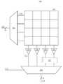
도 3a는 본 출원의 기술적 사상의 실시 예에 따른 시스템(391)의 일 실시 예를 보여주는 블록도이다. 도시된 실시 예에 있어서, 복수의 집적 회로 다이들(integrated circuit dies)이 스택되거나(stacked) 혹은 집적(integrated)되어 멀티-칩(multi-chip) 시스템을 형성한다. 다양한 실시 예들에 있어서, 이러한 멀티-칩 시스템(391)은, 앞서 설명된 바와 같이, RLUT를 포함할 것이다.FIG. 3A is a block diagram illustrating one embodiment of a
다양한 실시 예들에 있어서, 하이 밴드위스 메모리(High Bandwidth Memory, HBM)는 높은 퍼포먼스(performance)를 갖는 랜덤 액세스 메모리(random access memory)(이하, RAM)을 포함할 것이다. 몇몇의 실시 예들에 있어서, 하이 밴드위스 메모리는 쓰루-실리콘 비아(through-silicon via)(이하, TSV)를 이용하여 통신 동작을 수행하는 스택드 DRAM(stacked dynamic RAM)을 포함할 것이다. 일반적으로, 하이 밴드위스 메모리(HBM)는 쓰루-실리콘 비아들(TSVs)과 마이크로범프들(microbumps)을 결합하여 메모리 셀 어레이들의 복수의 다이(die)들(예를 들어, 4, 8개의 다이들)을 서로의 상부에 연결한다. 몇몇의 실시 예들에 있어서, 메모리 컨트롤러는 스택(stack)의 가장 하부(bottom)에 위치하는 독립적인 다이에 포함될 수 있다.In various embodiments, a High Bandwidth Memory (HBM) will include a random access memory (RAM) having high performance. In some embodiments, the high-band memory will include stacked dynamic RAM (DRAM) that performs communication operations using a through-silicon via (TSV). Generally, high bandwith memory (HBM) combines through-silicon vias (TSVs) and microbumps to form multiple die of memory cell arrays (e.g., four or eight die To the top of each other. In some embodiments, the memory controller may be included in an independent die located at the bottom of the stack.
다양한 실시 예들에 있어서, 시스템(391)은 하이 밴드위스 메모리를 포함할 것이다. 이러한 실시 예에 있어서, 시스템(391)은, 실시 예에 따라, 상부(top) 또는 하부(bottom) 또는 다른 곳에 위치하는 메모리 컨트롤러를 포함할 것이다. 한편, 상술한 설명은 예시적인 것이며, 본 출원의 기술적 사상은 이에 한정되지 않음이 이해될 것이다.In various embodiments, the
도시된 실시 예에 있어서, 시스템(391)은 (예를 들어, DRAM 등과 같은) 메모리 다이(304) 및 LUT 다이(LUTD)(302)를 포함할 것이다. 일 실시 예에 있어서, 메모리 다이(304) 및 LUT 다이(302)는 동일한 제조 공정을 사용하여 만들어지거나 혹은 동일하지 않은 제조 공정을 사용하여 만들어질 것이다.In the illustrated embodiment, the
도시된 실시 예에 있어서, 메모리 다이(304)는 복수의 메모리 어레이들(314)을 포함할 것이다. 이러한 실시 예에 있어서, 메모리 어레이들(314)은 다양한 조각들의 데이터를 저장하도록 구성될 것이다. 몇몇의 실시 예들에 있ㅇ서ㅓ, 데이터는 LUT 다이(302)에 의하여 액세스될 것이다.In the illustrated embodiment, the memory die 304 will comprise a plurality of memory arrays 314. In this embodiment, the memory arrays 314 will be configured to store various pieces of data. In some embodiments, the data will be accessed by the LUT die 302.
도시된 실시 예에 있어서, LUT 다이(302)는 하나 또는 그 이상의 재설정 가능한 LUT들(이하, RLUT)(312)을 포함할 것이다. RLUT(312)는, 앞서 설명된 바와 같이, 주어진 논리 연산을 수행할 수 있는 룩-업 테이블을 저장하도록 구성된 메모리 서브-어레이(memory sub-array)를 포함할 것이다. 앞서 설명된 바와 같이, 다양한 실시 예들에 있어서, RLUT(312)는 쓰기 요청들을 받아들여 메모리 서브-어레이가 논리 연산들을 가속(accelerating)하고 수행하는 프로그램 동작을 수행하도록 (도 3c에 도시된) 인터페이스를 포함할 것이다. 앞서 설명된 바와 같이, 다양한 실시 예들에 있어서, RLUT(312)는 읽기 요청들을 받아들여 룩-업 테이블에 저장된 논리 연산들의 수행을 야기하기 위한 인터페이스를 포함할 것이다.In the illustrated embodiment, LUT die 302 will include one or more resettable LUTs (hereinafter RLUT) 312.
다양한 실시 예들에 있어서, RLUT(312)는 하나 또는 그 이상의 비아들(vias)(326) (또는 마이크로범프들)을 이용하여 메모리(314)와 통신할 것이다. 이러한 실시 예는, (예를 들어, RLUT(312와 같은) 버스 또는 다른 외부 인터페이스를 통하여 통신할 필요 없이, 처리 소자(processing element)와 (예를 들어, 메모리(314)에) 저장된 데이터 사이의 빠른 통신을 가능하게 할 것이다.In various embodiments, the
다양한 실시 예들에 있어서, 메모리(314)는 입력들(322)을 RLUT(312)로 전송하고 출력들(324)을 RLUT(312)로부터 수신하기 위한 특정 인터페이스들을 포함할 것이다. 이러한 실시 예에 있어서, 메모리(314)는 RLUT(312)에 의하여 제기된(issued) 읽기 요청에 응답하여, 입력 값들(input values)이 입력 인터페이스(322)에 이용가능하도록 할 것이다. 이와 유사하게, 메모리(314)는 RLUT(312)에 의하여 제기된 쓰기 요청에 응답하여, 출력 인터페이스(324)에 이용가능한 출력 값들(output values)을 저장할 것이다. 다양한 실시 예들에 있어서, 이러한 읽기/쓰기 요청들은 전통적인 프로세서에 의하여 제기된 전통적인 읽기/쓰기 요청을 포함할 것이다. 다른 실시 예에 있어서, 읽기/쓰기 요청들은 입력 인터페이스(322)를 이용하여 원하는 데이터를 이용가능하게 만드는 전통적인 프로세서 또는 RLUT(312)에 의한 요청을 포함할 것이다. 이와 유사하게, 출력 인터페이스(324)에 보내진 데이이터를 저장하는 것에 역시 적용될 것이다. 다만, 상술한 설명은 예시적인 것이며, 본 출원의 기술적 사상은 이에 한정되지 않음이 이해될 것이다.In various embodiments, memory 314 may include specific interfaces for sending inputs 322 to
다양한 실시 예들에 있어서, RLUT(312)는 액세스된 메모리(314)에 같은 장소에 배치되거나 또는 물리적으로 근접할 것이다. 이러한 실시 예에 있어서, 둘 사이의 연결, 즉 액세스 타임 및 파워소모 모두가 줄어들 것 이다. 더욱이, 둘 사이에 요구되는 라우팅 역시 줄어들 것이다. 한편, 상술한 설명은 예시적인 것이며, 본 출원의 기술적 사상은 이에 한정되지 않음이 이해될 것이다.In various embodiments, the
몇몇의 실시 예들에 있어서, LUT 다이(302)는 (도면의 LUT 다이(302)에는 도시되지 않은) 하나 또는 그 이상의 메모리들(314)을 포함할 것이다. 이러한 실시 예에 있어서, RLUT(312)는 LUT 다이(302)의 메모리들(314) 또는 LUT 다이(304)의 메모리들(314) 중 어느 하나에 저장된 데이터에 액세스하도록 구성될 것이다. 다만, 상술한 설명은 예시적인 것이며, 본 출원의 기술적 사상은 이에 한정되지 않음이 이해될 것이다.In some embodiments, the LUT die 302 will include one or more memories 314 (not shown in the LUT die 302 of the drawing). In this embodiment, the
도 3b는 본 출원의 기술적 사상에 따른 시스템(392)의 일 실시 예를 보여주는 블록도이다. 도시된 실시 예에 있어서, 복수의 집적 회로 다이들(integrated circuit dies)이 스택되거나(stacked) 혹은 집적(integrated)되어 멀티-칩(multi-chip) 시스템 또는 하이밴드위스 메모리(high-bandwidth memory)를 형성한다. 다양한 실시 예들에 있어서, 이러한 멀티-칩 시스템(392)은, 앞서 설명된 바와 같이, RLUT를 포함할 것이다.FIG. 3B is a block diagram illustrating one embodiment of a
도시된 실시 예에 있어서, 시스템(392)은 (예를 들어, DRAM 등과 같은) 메모리 다이(304) 및 LUT 다이(LUTD)(302)를 포함할 것이다. 다양한 실시 예들에 있어서, 메모리 다이(304)는 복수의 메모리들(314)을 포함할 것이며, 각각은 대응하는 데이터 조각들을 저장하도록 구성될 것이다. 이러한 실시 예에 있어서, LUT 다이(302)는 RLUT(312)로 구성된 하나 또는 그 이상의 서브-어레이들을 포함할 것이다.In the illustrated embodiment, the
다양한 실시 예들에 있어서, 시스템(392)은 또한 라우팅 다이(306)를 포함할 것이다. 라우팅 다이(306)는 룩-업 테이블 다이(look-up table die)(312) 및 메모리 다이(304) 사이에서 신호들을 급격하게(dynamically) 라우팅 하도록 구성될 것이다. 다양한 실시 예들에 있어서. 라우팅 다이(306)는 하나 또는 그 이상의 비아들(326)에 의하여 LUT 다이(302)에 연결될 것이다. 비아들(326)(또는 그것의 일부)의 끝(end)은 입출력(input/output, I/O) 단자들 또는 인터페이스들(323)일 것이다. 이러한 실시 예에 있어서, 라우팅 다이(306)는 입출력 인터페이스(323) 및 원하는 데이터를 저장하는 메모리들(314) 사이에서 급격하게 신호들을 라우팅 할 것이다.In various embodiments, the
다양한 실시 예들에 있어서, 라우팅은 라우팅 구조(routing structure)(327)에 의하여 수행될 것이다. 다양한 실시 예들에 있어서, 라우팅 구조(327)는, 예를 들어, 멀티플렉서들(multiplexers), 디-멀티플렉서들(de-multiplexers), 크로스바 스위치들(crossbar switches), 로타리 스위치(rotary switch), 메모리 스위치(memory switch), 크로스오버 스위치(crossover switch) 등과 같은 다양한 라우팅 장치들을 포함할 것이다. 다만, 상술한 설명은 예시적인 것이며, 본 출원의 기술적 사상은 이에 한정되지 않음이 이해될 것이다.In various embodiments, the routing may be performed by a routing structure 327. In various embodiments, the routing structure 327 may include, for example, multiplexers, de-multiplexers, crossbar switches, rotary switches, memory switches, a memory switch, a crossover switch, and the like. It should be understood, however, that the above description is illustrative and that the technical idea of the present application is not limited thereto.
몇몇의 실시 예들에 있어서, 라우팅 구조(327)는 RLUT(312)의 입출력 인터페이스들(323) 및 메모리들(314)의 유사한 입출력 인터페이스들(323a 또는 323b) 사이에서 입출력 신호들을 라우팅하도록 구성될 것이다. 도시된 실시 예에 있어서, 두 개의 가능한 라우팅 스킴들이 도시되어 있다. 예를 들어, 직선은 RLUT(312)를 제 1 메모리(메모리 다이(304)의 왼쪽 아래 코너에 도시된 메모리))의 입출력 인터페이스(323a)에 연결하도록 사용될 제 1 라우트를 보여준다. 다른 예로, 점선은 RLUT(312)를 제 2 메모리(메모리 다이(304)의 오른쪽에 도시된 메모리)의 입출력 인터페이스(323b)에 연결하도록 사용될 제 2 라우트를 보여준다. 다만, 상술한 설명은 예시적인 것이며, 본 출원의 기술적 사상은 이에 한정되지 않음이 이해될 것이다.In some embodiments, routing structure 327 may be configured to route input / output signals between input / output interfaces 323 of
이러한 실시 예에 있어서, 정확한 라우팅은 RLUT(312) 및 액세스될 데이터에 의하여 수행될 논리 연산에 기초하여 다를 것이다. 예를 들어, 만약 RLUT(312)에 의하여 액세스될 데이터가 제 1 메모리에 저장된다면, 직선(solid line)의 라우트가 사용될 것이다. 그러나, 만약 RLUT(312)에 의하여 액세스될 데이터가 제 2 메모리에 저장되어 있다면, 점선의 라우트가 대신 사용될 것이다. 다양한 실시 예들에 있어서, 신호 라우팅은 RLUT(312)의 논리 연산 또는 RLUT(312)에 의하여 액세스된 데이터의 변화에 응답하여 급격하게 변할 것이다.In this embodiment, the correct routing will be different based on the logical operations to be performed by the
도 3c는 본 출원의 기술적 사상의 실시 예에 따른 시스템(393)의 일 예를 보여주는 블록도이다. 도시된 실시 예에 있어서, 복수의 집적 회로 다이들(integrated circuit dies)이 스택되거나(stacked) 혹은 집적(integrated)되어 멀티-칩(multi-chip) 시스템 또는 하이밴드위스 메모리(high-bandwidth memory)를 형성할 것이다. 다양한 실시 예들에 있어서, 이러한 멀티-칩 시스템(393)은, 앞서 설명된 바와 같이, RLUT를 포함할 것이다.3C is a block diagram illustrating an example of a
도시된 실시 예에 있어서, 앞서 설명된 바와 같이, 시스템(393)은 (예를 들어, DRAM 등과 같은) 메모리 다이(304) 및 LUT 다이(LUTD)(302)를 포함할 것이다. 다양한 실시 예들에 있어서, 메모리 다이(304)는 복수의 메모리들(314)을 포함할 것이며, 각각은 대응하는 데이터 조각들을 저장하도록 구성될 것이다. 이러한 실시 예에 있어서, LUT 다이(302)는 RLUT(312)로 구성된 하나 또는 그 이상의 서브-어레이들을 포함할 것이다.In the illustrated embodiment, as described above, the
도시된 실시 예에 있어서, 시스템(393)은 또한 프로세서 다이(processor die)(308)를 포함할 것이다. 다양한 실시 예들에 있어서, 프로세서 다이(308)는 실질적으로 논리 연산들을 전용적으로 수행하는 복수의 고정된 논리 회로(318)를 포함할 것이며, RLUT들(312)이 변경됨에 따라 변경되지 않을 것이다. 다양한 실시 예들에 있어서, 고정된 논리 회로들(318)은 하나 또는 그 이상의 프로세서 코어들을 포함할 것이다. 더욱이, 일 실시 예에 있어서, 프로세서 다이(308)는 메모리 다이(304) 또는 LUT 다이(302)를 생성하는데 사용되는 프로세스와 다른 방법을 사용하여 제조될 수도 있으며, 그렇지 않을 수도 있다. 몇몇의 실시 예들에 있어서, 시스템(393)은 시스템-온-칩(SoC)을 포함할 것이다. 한편, 상술한 설명은 예시적인 것이며, 본 출원의 기술적 사상은 이에 한정되지 않음이 이해될 것이다.In the illustrated embodiment, the
다양한 실시 예들에 있어서, 프로세서 다이(308)는 RLUT 다이(312)를 설정(establish)하거나 이용할 것이다. 이러한 실시 예에 있어서, (LUT 다이(302)의) LUT 인터페이스(316)를 거쳐 RLUT(312)에 쓰기 동작을 하거나 RLUT(312)로부터 읽기 동작을 수행할 것이다. 앞서 설명된 바와 같이, 다양한 실시 예들에 있어서, LUT 인터페이스(316)는 쓰기 요청들을 받아들여 메모리 서브-어레이가 논리 연산들을 가속(accelerating)하고 실행하는 프로그램 동작을 수행하도록 쓰기 요청들을 받아들이도록(accept) 구성될 것이다. 또한, 앞서 설명된 바와 같이, 다양한 실시 예들에 있어서, LUT 인터페이스(316)는 룩-업 테이블에 저장된 논리 연산들의 수행을 야기하기 위한 읽기 요청들을 받아들이도록 구성될 것이다.In various embodiments, processor die 308 may establish or utilize RLUT die 312. In this embodiment, a write operation to the
다양한 실시 예들에 있어서, 프로세서 다이(308)는 하나 또는 그 이상의 RLUT(312)를 포함할 것이다. 몇몇의 실시 예들에 있어서, 본 출원의 기술적 사상에 따른 실시 예는 메모리 다이(304) 및 프로세서 다이(308)를 포함할 것이며, 프로세서 다이(308)는 RLUT(312)를 포함하되 LUT 다이(302)와 별도의 구성이 아닐 수 있다. 이러한 실시 예에 있어서, 프로세서 다이(308)는 LUT 다이(302)로 개념적으로 보일 수 있다. 한편, 상술한 설명은 예시적인 것이며, 본 출원의 기술적 사상은 이에 한정되는 것이 아님이 이해될 것이다.In various embodiments, the processor die 308 may include one or
도 4는 본 출원의 기술적 사상의 실시 예에 따른 시스템들(490, 492, 494)의 예들을 보여주는 블록도이다. 도시된 실시 예에 있어서, 복수의 집적 회로 다이들(integrated circuit dies)이 스택되거나(stacked) 혹은 집적(integrated)되어 멀티-칩(multi-chip) 시스템 또는 하이 밴드위스 메모리(high-bandwidth memory)를 형성할 것이다. 다양한 실시 예들에 있어서, 이러한 멀티-칩 시스템들(490, 492, 494)은, 앞서 설명된 바와 같이, RLUT를 포함할 것이다.4 is a block diagram illustrating examples of
도시된 실시 예에 있어서, 시스템(490)은 메모리 도는 DRAM 다이(304), 라우팅 다이(306), LUT 다이(302), 그리고 논리 또는 프로세서 다이(308)를 포함할 것이다. 일 실시 예에 있어서, 라우팅 다이(306)는 메모리 다이(304)와 LUT 다이(302) 사이에 위치하여 둘 사이의 신호들을 라우팅하는 것을 용이하게 할 것이다. 도시된 실시 예에 있어서, 프로세서 다이(308)는 스택의 하부(bottom)에 위치할 것이다. 몇몇의 실시 예들에 있어서, 프로세서 다이(308)는 메모리 다이(304) 또는 LUT 다이(302)로부터 서로 다른 기술 또는 프로세스를 사용하여 조작(fabricated)될 것이다. 한편, 상술한 설명은 예시적인 것이며, 본 출원의 기술적 사상은 이에 한정되지 않음이 이해될 것이다.In the illustrated embodiment, the
도시된 실시 예에 있어서, 시스템(492)은 복수의 메모리 다이들(304), 라우팅 다이(306), LUT 다이(302), 그리고 논리 또는 프로세서 다이(308)를 포함할 것이다. 일 실시 예에 있어서, 라우팅 다이(306)는 복수의 메모리 다이들(304) 및 LUT 다이(302) 사이에 위치하여 둘 사이의 신호들을 라우팅하는 것을 용이하게 할 것이다. 도시된 실시 예에 있어서, 프로세서 다이(308)는 스택의 하부에 위치할 것이다. 한편, 상술한 설명은 예시적인 것이며, 본 출원의 기술적 사상은 이에 한정되지 않음이 이해될 것이다.In the illustrated embodiment, the
도시된 실시 예에 있어서, 시스템(494)은 복수의 메모리 다이들(304), LUT 다이(302), 그리고 논리 또는 프로세서 다이(308)를 포함할 것이다. 일 실시 예에 있어서, 라우팅 다이(306)가 (적어도 메모리 다이들(304) 및 LUT 다이(302) 사이에는) 존재하지 않을 것이다. 이러한 실시 예에 있어서, LUT 다이(302) 및 메모리 다이(304)는 스트레이트-쓰루 비아들(straight-through vias) 또는 다른 수단들을 사용하여 통신할 것이다. 몇몇의 실시 예들에 있어서, LUT 다이(302)는 단지 최근접 또는 인접하는 메모리 다이(304)와 통신할 것이다. 한편, 상술한 설명은 예시적인 것이며, 본 출원의 기술적 사상은 이에 한정되지 않음이 이해될 것이다.In the illustrated embodiment, the
한편, 상술한 설명들 및 도시된 실시 예들은 단지 본 출원의 기술적 사상의 몇몇 실시 예들에 불과할 뿐, 본 출원의 기술적 사상을 한정하는 것은 아님이 이해될 것이다. 예를 들어, 다른 실시 예에 있어서, 복수의 라우팅 다이들(302)이 사용될 수 있다. 예를 들어, 제 1 라우팅 다이(306)가 프로세서 다이(308) 및 LUT 다이(302) 사이에 존재할 것이며, 제 2 라우팅 다이(306)가 메모리 다이(304)와 LUT 다이(302) 사이에 존재할 것이다.It is to be understood, however, that the foregoing description and illustrated embodiments are merely illustrative of some of the technical aspects of the present application and are not intended to limit the scope of the present application. For example, in other embodiments, a plurality of routing dies 302 may be used. For example, a first routing die 306 may exist between the processor die 308 and the LUT die 302 and a second routing die 306 may exist between the memory die 304 and the LUT die 302 will be.
다른 실시 예에 있어서, 둘 또는 그 이상의 다이들은 스택되는 대신에 나란히(side-by-side) 배열될 수 있을 정도로 충분히 작을 수 있다. 예를 들어, 일 실시 예에 있어서, 논리 또는 프로세서 다이(308) 및 LUT 다이(302)는 함께 메모리 다이(304)와 대략 동일한 크기일 수 있다. 이러한 실시 예에 있어서, 프로세서 다이(308)와 LUT 다이(302)는 하나의 레벨 상에 나란히 위치할 것이며, 메모리 다이(304)가 두 다이들(302, 308) 위에 또는 아래에 위치할 것이다. 이러한 실시 예에 있어서, 데이터는 데이터가 저장될 실행 소자(execution element)(예를 들어, LUT, 고정 회로 등)와 같은 위치 또는 인접한 장소에 저장될 것이다. 한편, 상술한 설명은 예시적인 것이며, 본 출원의 기술적 사상은 이에 한정되지 않음이 이해될 것이다.In other embodiments, two or more dies may be small enough to be arranged side-by-side instead of being stacked. For example, in one embodiment, the logic or processor die 308 and the LUT die 302 may be approximately the same size as the memory die 304 together. In this embodiment, the processor die 308 and the LUT die 302 will be positioned side by side on one level and the memory die 304 will be located on or below the two dies 302, 308. In this embodiment, the data will be stored at a location, such as an execution element (e.g., LUT, fixed circuit, etc.) where the data is to be stored or in an adjacent location. It should be understood, however, that the above description is exemplary and that the technical idea of the present application is not limited thereto.
다양한 실시 예들에 있어서, 스택된 LUT 다이(302) 시스템들을 위한 응용들은 빅 데이터(big data) 분석, 데이터 베이스, 하이 퍼포먼스 컴퓨팅 등을 포함할 것이다. 몇몇의 실시 예들에 있어서, LUT 다이(302)에 의하여 처리되는 데이터의 양은 (메모리 다이(304)와 같은) 데이터 스토리지가 제공할 충분한 이점들에 버금갈 만큼 충분히 크거나 빈번할 것이다. 한편, 상술한 설명은 예시적인 것이며, 본 출원의 기술적 사상은 이에 한정되는 것이 아님이 이해될 것이다.In various embodiments, applications for stacked LUT die 302 systems will include big data analysis, databases, high performance computing, and the like. In some embodiments, the amount of data processed by the LUT die 302 may be large enough or frequent enough to equal merely the advantages that the data storage (such as the memory die 304) will provide. It should be understood, however, that the above description is exemplary and that the technical idea of the present application is not limited thereto.
도 5는 본 출원의 기술적 사상의 실시 예에 따른 반도체 장치들을 포함하는 정보 처리 시스템(500)을 보여주는 블록도이다.5 is a block diagram showing an
도 5를 참조하면, 정보 처리 시스템(500)은 본 출원의 기술적 사상에 따라 구성된 하나 또는 그 이상의 장치들을 포함한다. 다른 실시 예에 있어서, 정보 처리 시스템(500)은 본 출원의 기술적 사상에 따른 하나 또는 그 이상의 기술들을 사용할 것이다.Referring to FIG. 5, the
다양한 실시 예들에 있어서, 정보 처리 시스템(500)은 랩톱, 데스크톱, 워크스테이션, 서버, 블래이드 서버(blade server), 개인용 디지털 장비, 스마트 폰, 태블릿 및 다른 적당한 컴퓨터 장치 또는 가상 머신(virtual machine) 또는 가상 컴퓨팅 장치와 같은 컴퓨팅 장치를 포함할 것이다. 다양한 실시 예들에 있어서, 정보 처리 장치(500)는 사용자에 의하여 의하여 사용될 것이다.In various embodiments, the
본 출원의 기술적 사상의 실시 예에 따른 정보 처리 장치(500)는 중앙 처리 장치(CPU), 논리 또는 프로세서(510)를 더 포함할 것이다. 몇몇의 실시 예에 있어서, 프로세서(510)는 하나 또는 그 이상의 기능 유닛 블록들(functional unit blocks, FUBs) 또는 조합 논리 블록들(combinational logic blocks, CLBs)을 포함할 것이다. 이러한 실시 예에 있어서, 조합 논리 블록은 다양한 Boolean 논리 동작들(예를 들어, NAND, NOR, NOT, XOR 등), 안정화 논리 장치들(예를 들어, 플립-플롭, 래치 등), 다른 논리 장치들 또는 이들의 조합을 포함할 서이다. 이러한 조합 논리 동작들은 원하는 결과를 얻기 위하여 입력 신호들을 단순하게 또는 복잡하게 처리하도록 구성될 것이다. 한편, 몇몇의 예시적인 실시 예들이 동기 조합 논리 동작들(synchronous combinational logic operations)의 예로써 설명되었으나, 본 출원의 기술적 사상은 이에 한정되지 않으며, 비동기식 동작들 또는 이들의 조합을 포함할 수 있음이 이해될 것이다. 일 실시 예로, 조합 논리 동작들은 복수의 CMOS 트랜지스터들을 포함할 수 있다. 다양한 실시 예들에 있어서, 이러한 CMOS 트랜지스터들은 논리 동작들을 수행하는 게이트들로 배열될 수 있다. 다만, 다양한 기술들이 본 출원의 기술적 사상의 범주 내에서 사용될 수 있음이 이해도리 것이다.The
본 출원의 기술적 사상에 따른 정보 처리 시스템(500)은 (예를 들어, RAM과 같은) 휘발성 메모리(520)를 포함할 것이다. 본 출원의 기술적 사상에 따른 정보 처리 시스템(500)은 (예를 들어, 하드 드라이브, 광학 메모리, NAND 또는 플래시 메모리 등과 같은) 불휘발성 메모리(530)를 포함할 것이다. 몇몇의 실시 예들에 있어서, 휘발성 메모리(520), 불휘발성 메모리(530) 또는 이들의 조합 또는 그 일부는 “저장 매체(storage medium)”라 칭해질 수 있다. 다양한 실시 예들에 있어서, 휘발성 메모리(520) 및/또는 불휘발성 메모리(530)는 반영구적이거나 실질적으로 영구적으로 데이터를 저장하도록 구성될 것이다.The
다양한 실시 예들에 있어서, 정보 처리 시스템(500)은 통신 네트워크를 통하여 통신할 수 있도록 하나 또는 그 이상의 네트워크 인터페이스(540)를 포함할 것이다. Wi-Fi 프로토콜의 예의 경우, IEEE 802.11g, IEEE 802.11n 등을 포함할 것이나, 이에 한정되는 것은 아니다. 셀룰러 프로토콜(cellular protocol)의 경우에 IEEE 802.16m (a.k.a. Wireless-MAN (Metropolitan Area Network) Advanced), Long Term Evolution (LTE) Advanced), Enhanced Data rates for GSM (Global System for Mobile Communications) Evolution (EDGE), Evolved High-Speed Packet Access (HSPA+) 등을 포함할 것이나, 이에 한정되는 것은 아니다. 유선 프로토콜의 경우에 IEEE 802.3 (a.k.a. Ethernet), Fibre Channel, Power Line communication(e.g., HomePlug, IEEE 1901, etc.) 등을 포함할 것이나, 이에 한정되는 것은 아니다. 한편, 상술한 설명은 예시적인 것이며, 본 출원의 기술적 사상은 이에 한정되는 것이 아님이 이해될 것이다.In various embodiments, the
본 출원의 기술적 사상의 실시 예에 다른 정보 처리 시스템(500)은 (예를 들어, 디스플레이 어댑터, 촉각 인터페이스, 휴먼 인터페이스 장치 등과 같은) 사용자 인터페이스 유닛(550)을 더 포함할 것이다. 다양한 실시 예들에 있어서, 이러한 사용자 인터페이스 유닛(550)은 사용자로부터 입력을 수신하거나 또는 사용자로 출력을 제공하도록 구성될 수 있다. 다른 종류의 장치들은 사용자에게 인터페이스를 제공하도록 사용될 수 있다. 예를 들어, 사용자로부터 제공되는 피드백은 어떠한 형태의 센서 피드백, 예를 들어, 시각 피드백(visual feedback), 청각 피드백(auditory feedback) 또는 촉각 피드백(tactile feedback) 등 일 수 있다. 사용자로부터의 입력은 음향(acoustic), 스피치(speech) 또는 촉각 입력일 수 있다.Other
다양한 실시 예들에 있어서, 정보 처리 시스템(500)은 (예를 들어, 디스플레이 또는 모니터, 키보드, 마우스, 카메라, 핑거프린트 리더, 비디오 프로세서 등과 같은) 하나 또는 그 이상의 장치들 또는 하드웨어 구성들(560)을 포함할 수 있다. 다만, 상술한 설명은 예시적인 것이며, 본 출원의 기술적 사상은 이에 한정되지 않음이 이해될 것이다.In various embodiments, the
본 출원의 기술적 사상의 실시 예에 따른 정보 처리 시스템(500)은 하나 또는 그 이상의 버스들(505)을 더 포함할 것이다. 이러한 실시 예에 있어서, 시스템 버스(505)는 프로세서(510), 휘발성 메모리(520), 불휘발성 메모리(530), 네트워크 인터페이스(540), 사용자 인터페이스 유닛(550) 그리고 하나 또는 그 이상의 하드웨어 구성들(560)에 통신적으로 연결되도록 구성될 것이다. 프로세서(510)에 의하여 처리되는 데이터 또는 불휘발성 메모리(530)의 외부로부터 입력되는 데이터가 불휘발성 메모리(530) 또는 휘발성 메모리(520) 중 어느 하나에 저장될 수 있다.The
다양한 실시 예들에 있어서, 정보 처리 시스템(500)은 하나 또는 그 이상의 소프트웨어 소자들(570)을 포함할 것이다. 몇몇의 실시 예에 있어서, 소프트웨어 소자들(570)은 OS(operating system) 및/또는 어플리케이션을 포함할 것이다. 몇몇의 실시 예에 있어서, OS는 어플리케이션에 하나 또는 그 이상의 서비스들을 제공하도록 구성되며, 정보 처리 시스템(500)의 어플리케이션과 다양한 하드웨어 소자들(예를 들어, 프로세서(510), 네트워크 인터페이스(540) 등) 사이의 중개자(intermediary)로서 관리하거나 동작할 것이다. 이러한 실시 예에 있어서, 정보 처리 시스템(500)은 (불휘발성 메모리(530) 내부 등에) 지엽적으로 설치되고 프로세서(510)에 의하여 직접적으로 실행되며 OS와 직접적으로 상호 동작하도록 구성된 하나 또는 그 이상의 네이티브 어플리케이션(native application)을 포함할 것이다. 이러한 실시 예에 있어서, 네이티브 어플리케이션들은 코드(code)를 실행할 수 있는 프리-컴파일드 머신(pre-compiled machine)을 포함할 것이다. 몇몇의 실시 예들에 있어서, 네이티브 어플리케이션들은 소스(source) 또는 오브젝트(object) 코드를 프로세서(510)에 의하여 실행 가능한 코드로 해석하도록 구성되는 (C shell(csh), AppleScript, AutoHotkey 등의)스크립트 번역기(script interpreter) 또는 (Java Virtual Machine, Microsoft Common Language Runtime 등의) 가상 실행 머신(virtual execution machine, VM)을 포함할 것이다.In various embodiments, the
앞서 설명된 반도체 장치들은 다양한 패키징 기술들을 이용하여 캡슐화(encapsulate)될 것이다. 예를 들어, 본 출원의 기술적 사상에 따라 구현된 반도체 장치들은 POP(package on package) 기술, BGAs(ball grid arrays) 기술, CSPs(chip scale packages) 기술, PLCC(plastic leaded chip carrier) 기술, PDIP(plastic dual in-line package) 기술, 다이 인 와플 팩(die in waffle pack) 기술, 다이 인 와퍼 폼(die in wafer form) 기술, COB(chip on board) 기술, CERDIP(ceramic dual in-line package) 기술, PMQFP(plastic metric quad flat package) 기술, PQFP(plastic quad flat package) 기술, SOIC(small outline package) 기술, SSOP(shrink small outline package) 기술, TSOP(thin small outline package) 기술, TQFP(thin quad flat package) 기술, SIP(system in package) 기술, MCP(multi-chip package) 기술, WFP(wafer-level fabricated package) 기술, WSP(wafer-level processed stack package) 기술 또는 본 출원의 기술분야에서 통상의 지식을 가진 자에게 잘 알려진 기술 중 어느 하나를 사용하여 캡슐화될 것이다.The semiconductor devices described above will be encapsulated using various packaging techniques. For example, the semiconductor devices implemented in accordance with the technical idea of the present application may be implemented on a package-on-package (POP) technology, ball grid array (BGAs) technology, chip scale packages (CSPs) technology, plastic leaded chip carrier die in wafer form technology, chip on board (COB) technology, ceramic dual in-line package (CERDIP) technology, plastic dual in-line package technology, die in waffle pack technology, ), Plastic metric quad flat package (PMQFP) technology, plastic quad flat package (PQFP) technology, small outline package (SOIC) technology, shrink small outline package (SSOP) technology, thin small outline package (TSOP) thin quad flat package, SIP, multi-chip package (MCP), wafer-level fabricated package (WFP), wafer-level processed stack package (WSP) Using techniques well known to those of ordinary skill in the art.
방법 단계들은 컴퓨터 프로그램을 수행하여 입력 데이터를 동작시키고 출력 데이터를 발생시키는 기능들을 수행하는 하나 또는 그 이상의 프로그램 가능한 프로세서들에 의하여 수행될 것이다. 방법 단계들은 도한 FPGA(field programmable gate array) 또는 ASIC(application-specific integrated circuit) 등과 같은 특수 목적의 논리 회로에 의하여 동작하거나, 장치는 이러한 특수 목적의 논리 회로로써 구현될 것이다.The method steps may be performed by one or more programmable processors that perform the functions of performing a computer program to operate input data and generate output data. The method steps may be implemented by special purpose logic circuits, such as field programmable gate arrays (FPGAs) or application-specific integrated circuits (ASICs), or the devices may be implemented as such special purpose logic circuits.
다양한 실시 예들에 있어서, 컴퓨터 판독 가능한 매체는 동작할 때에 장치로 하여금 방법 단계들 중 적어도 일부를 수행하도록 하는 인스트럭션들을 포함할 것이다. 몇몇의 실시 예들에 있어서, 컴퓨터 판독 가능한 매체는 자기 매체(magnetic medium), 광학 매체(optical medium), 다른 매체, 또는 이들의 조합(예를 들어, CD-ROM, 하드 드라이브, ROM, 플래시 드라이브 등)에 포함될 것이다. 이러한 실시 예에 있어서, 컴퓨터 판독 가능한 매체는 제조 시에 실체적(tangibly) 또는 비-일시적(non-transitorily)인 성질을 갖도록 구현될 수 있다.In various embodiments, the computer-readable medium will include instructions that, when actuated, cause the device to perform at least some of the method steps. In some embodiments, the computer-readable medium can be a magnetic medium, optical medium, other medium, or a combination thereof (e.g., CD-ROM, hard drive, ROM, ). In such an embodiment, the computer-readable medium may be implemented to have a property that is tangibly or non-transitorily at the time of manufacture.
본 출원의 기술적 사상에 따른 실시 예들이 앞서 설명되었다. 다만 상술한 설명은 예시적인 것이며, 본 출원의 기술적 사상을 벗어나지 않은 채로 본 출원의 기술적 사상의 범주 내에서 다양하게 적용 및 응용될 수 있을 것이다. 따라서, 본 출원의 기술적 사상은 앞서 설명된 실시 예들에 한정되지 않음이 이해될 것이다. 따라서, 본 출원의 기술적 사상의 범주는 본 출원의 청구항을 가능한 넓게 해석하거나 이와 균등하게 해석하는 것에 의하여 정하여 질 것이며, 앞서 설명된 실시 예들에 의하여 한정되지 않는다. 또한, 본 출원의 청구항은 본 출원의 실시 예들이 그 범위 내에서 다양하게 변경되거나 변형된 실시 예들을 포함하도록 의도된 것들임이 이해될 것이다.Embodiments according to the technical idea of the present application have been described above. It is to be understood that both the foregoing general description and the following detailed description are exemplary and explanatory only and are not restrictive of the invention, as claimed. Therefore, it will be understood that the technical idea of the present application is not limited to the embodiments described above. Accordingly, the scope of the technical idea of the present application will be determined by broadly construing or evenly interpreting the claims of the present application as possible, and is not limited by the embodiments described above. It is also to be understood that the claims of the present application are intended to encompass embodiments in which the present application is variously modified or modified within its scope.
102: 재설정 가능 메모리 로직
104: 프로세서
106, 314: 메모리
108: 기타 구성들
112: 처리 소자(RLUT)
114: 램(RAM)
116: 설정 인터페이스
118: 입출력 인터페이스
200, 312: 재설정 가능 룩-업 테이블(RLUT)
202: 메모리 셀들
204: 로컬 로우 디코더
206: 드라이버
208: 로컬 라인 선택기
302: 룩-업 테이블(LUT) 다이
304: 메모리 다이
306: 라우팅 다이
312: 재설정 가능 룩-업 테이블(RLUT) 다이
322: 입력 인터페이스
324: 출력 인터페이스
391, 392, 393: 멀티 칩 시스템
490, 494, 494: 시스템들
500: 정보 처리 시스템102: Resettable memory logic
104: Processor
106, 314: memory
108: Other configurations
112: Processing element (RLUT)
114: RAM (RAM)
116: Configuration Interface
118: Input / output interface
200, 312: a reconfigurable look-up table (RLUT)
202: memory cells
204: local row decoder
206: Driver
208: Local line selector
302: look-up table (LUT) die
304: Memory die
306: Routing die
312: Resettable look-up table (RLUT) die
322: input interface
324: Output interface
391, 392, 393: Multi-chip system
490, 494, 494: Systems
500: Information processing system
Claims (10)
Translated fromKorean상기 장치는 복수의 스택된 집적 회로 다이들을 포함하며,
상기 복수의 스택된 집적 회로 다이들은
랜덤 액세스 방식으로 데이터를 저장하도록 구성된 메모리 셀 다이; 및
논리 연산을 수행하도록 구성된 재설정 가능한 룩-업 테이블을 포함하는 랜덤 액세스 메모리 어레이를 포함하는 룩-업 테이들 다이를 포함하고,
상기 재설정 가능한 룩-업 테이블은
논리 연산을 수행하는 룩-업 테이블을 저장하도록 구성된 복수의 랜덤 액세스 메모리 셀들; 및
입력 신호들의 세트에 기초하여 메모리 셀들의 하나 또는 그 이상의 행들을 활성화하는 로컬 로우 디코더를 포함하고,
상기 복수의 메모리 셀들에 저장된 상기 룩-업 테이블은 메모리 쓰기 동작을 통하여 상기 랜덤 액세스 메모리 어레이로 변경되는, 장치.In the apparatus,
The apparatus includes a plurality of stacked integrated circuit dies,
The plurality of stacked integrated circuit dies
A memory cell die configured to store data in a random access manner; And
A look-up table die including a random access memory array including a reconfigurable look-up table configured to perform logical operations,
The reconfigurable look-up table
A plurality of random access memory cells configured to store a look-up table performing logical operations; And
A local row decoder for activating one or more rows of memory cells based on the set of input signals,
Wherein the look-up table stored in the plurality of memory cells is changed to the random access memory array through a memory write operation.
상기 복수의 스택된 집적 회로 다이들은 고정된 논리 회로들을 포함하는 논리 다이를 포함하는, 장치.The method according to claim 1,
Wherein the plurality of stacked integrated circuit dies includes a logic die comprising fixed logic circuits.
상기 재설정 가능한 룩-업 테이블은
상기 메모리 셀 다이 도는 상기 논리 다이 중 어느 하나로부터 데이터를 수신하고,
상기 논리 다이로부터의 도움 없이, 상기 데이터에 대한 상기 논리 연산을 수행하고,
상기 메모리 셀 다이 또는 상기 논리 다이 중 어느 하나에 출력을 제공하는, 장치.3. The method of claim 2,
The reconfigurable look-up table
Wherein the memory cell die receives data from any of the logic dice,
Perform the logical operation on the data without assistance from the logic die,
And provide an output to either the memory cell die or the logic die.
상기 복수의 스택된 집적 회로 다이들은 상기 메모리 셀 다이 및 상기 룩-업 테이블 다이 사이에서 신호들을 라우팅 하도록 구성된 라우팅 다이를 포함하는, 장치.The method according to claim 1,
Wherein the plurality of stacked integrated circuit dies includes a routing die configured to route signals between the memory cell die and the look-up table die.
상기 복수의 스택된 집적 회로 다이들은 복수의 메모리 셀 다이들을 포함하며,
상기 라우팅 다이는 상기 룩-업 테이블 다이 및 상기 복수의 메모리 셀 다이들 사이에서 신호들을 라우팅 하도록 구성되며,
상기 라우팅 다이에 의하여 제공되는 신호 라우팅은 상기 룩-업 테이블 다이의 논리 연산의 변화에 응답하여 변경되도록 구성되는, 장치.5. The method of claim 4,
The plurality of stacked integrated circuit dies including a plurality of memory cell dice,
Wherein the routing die is configured to route signals between the look-up table die and the plurality of memory cell dies,
Wherein the signal routing provided by the routing die is configured to change in response to a change in the logical operation of the look-up table die.
상기 메모리 셀 다이 및 상기 룩-업 테이블 다이는 동일한 제작 기술에 의하여 제조되는, 장치.The method according to claim 1,
Wherein the memory cell die and the look-up table die are manufactured by the same fabrication technique.
상기 메모리 셀 다이는 하이 밴드위스 메모리를 포함하는, 장치.The method according to claim 1,
Wherein the memory cell die comprises a high bandwith memory.
상기 재설정 가능한 룩-업 테이블은 상기 재설정 가능한 룩-업 테이블에 의하여 처리되는 데이터를 저장하는 상기 메모리 셀 다이의 일부분에 물리적으로 근접하도록 상기 룩-업 테이블 다이에 물리적으로 위치하는, 장치.The method according to claim 1,
Wherein the reconfigurable look-up table is physically located on the look-up table die such that the reconfigurable look-up table is physically proximate to a portion of the memory cell die storing data processed by the reconfigurable look-up table.
프로세서 코어를 포함하는 프로세서 다이를 포함하며,
상기 룩-업 테이블 다이는 논리 연산을 수행하는 룩-업 테이블을 저장하는 복수의 랜덤 액세스 메모리 셀들을 포함하고,
상기 룩-업 테이블은 메모리 쓰기 동작에 의하여 랜덤 액세스 메모리 셀들로 변경되며,
상기 프로세서 코어는 상기 논리 연산의 수행에 대한 부담을 상기 재설정 가능한 룩-업 테이블로 전이하는, 시스템 온 칩.A look-up table die comprising a reconfigurable look-up table configured to perform logical operations; And
A processor die including a processor core,
Wherein the look-up table die comprises a plurality of random access memory cells storing a look-up table performing logical operations,
The look-up table is changed to random access memory cells by a memory write operation,
Wherein the processor core transitions the burden of performing the logical operation to the reconfigurable look-up table.
상기 룩-업 테이블 다이 및 프로세서 다이는 쓰루-실리콘 비아들에 의하여 전기적으로 연결된, 시스템 온 칩.10. The method of claim 9,
Wherein the look-up table die and the processor die are electrically connected by through-silicon vias.
Applications Claiming Priority (8)
| Application Number | Priority Date | Filing Date | Title |
|---|---|---|---|
| US201462092819P | 2014-12-16 | 2014-12-16 | |
| US201462092825P | 2014-12-16 | 2014-12-16 | |
| US201462092822P | 2014-12-16 | 2014-12-16 | |
| US62/092,825 | 2014-12-16 | ||
| US62/092,819 | 2014-12-16 | ||
| US62/092,822 | 2014-12-16 | ||
| US14/838,347US9577644B2 (en) | 2014-12-16 | 2015-08-27 | Reconfigurable logic architecture |
| US14/838,347 | 2015-08-27 |
Publications (2)
| Publication Number | Publication Date |
|---|---|
| KR20160073334Atrue KR20160073334A (en) | 2016-06-24 |
| KR102440132B1 KR102440132B1 (en) | 2022-09-05 |
Family
ID=56112171
Family Applications (3)
| Application Number | Title | Priority Date | Filing Date |
|---|---|---|---|
| KR1020150179353AActiveKR102496680B1 (en) | 2014-12-16 | 2015-12-15 | Dram-based reconfigurable logic |
| KR1020150180209AActiveKR102438730B1 (en) | 2014-12-16 | 2015-12-16 | DRAM-based reconfigurable logic device supporting spatial multiplexing |
| KR1020150180208AActiveKR102440132B1 (en) | 2014-12-16 | 2015-12-16 | Reconfigurable logic architecture |
Family Applications Before (2)
| Application Number | Title | Priority Date | Filing Date |
|---|---|---|---|
| KR1020150179353AActiveKR102496680B1 (en) | 2014-12-16 | 2015-12-15 | Dram-based reconfigurable logic |
| KR1020150180209AActiveKR102438730B1 (en) | 2014-12-16 | 2015-12-16 | DRAM-based reconfigurable logic device supporting spatial multiplexing |
Country Status (5)
| Country | Link |
|---|---|
| US (3) | US9954533B2 (en) |
| JP (1) | JP6594762B2 (en) |
| KR (3) | KR102496680B1 (en) |
| CN (1) | CN105703765B (en) |
| TW (1) | TWI649970B (en) |
Cited By (1)
| Publication number | Priority date | Publication date | Assignee | Title |
|---|---|---|---|---|
| KR20210013870A (en)* | 2019-07-29 | 2021-02-08 | 에스케이하이닉스 주식회사 | Memory system for data swap and method operating thereof |
Families Citing this family (45)
| Publication number | Priority date | Publication date | Assignee | Title |
|---|---|---|---|---|
| US10013212B2 (en)* | 2015-11-30 | 2018-07-03 | Samsung Electronics Co., Ltd. | System architecture with memory channel DRAM FPGA module |
| US10848158B2 (en) | 2016-02-13 | 2020-11-24 | HangZhou HaiCun Information Technology Co., Ltd. | Configurable processor |
| US20170322906A1 (en)* | 2016-05-04 | 2017-11-09 | Chengdu Haicun Ip Technology Llc | Processor with In-Package Look-Up Table |
| US10075168B2 (en)* | 2016-03-05 | 2018-09-11 | XiaMen HaiCun IP Technology LLC | Configurable computing array comprising three-dimensional writable memory |
| JP2017169118A (en)* | 2016-03-17 | 2017-09-21 | 株式会社東芝 | Integrated circuit and electronic equipment |
| CN107346352A (en)* | 2016-05-04 | 2017-11-14 | 杭州海存信息技术有限公司 | Emulation processor based on look-up table in encapsulation |
| US9871020B1 (en)* | 2016-07-14 | 2018-01-16 | Globalfoundries Inc. | Through silicon via sharing in a 3D integrated circuit |
| US10354716B2 (en) | 2016-09-16 | 2019-07-16 | Aspiring Sky Co. Limited | SRAM based memory structures and methods thereof |
| US11361813B2 (en) | 2016-09-16 | 2022-06-14 | Aspiring Sky Co. Limited | Nonvolatile memory structures with DRAM |
| US10402342B2 (en)* | 2016-10-20 | 2019-09-03 | Aspiring Sky Co., Limited | Re-configurable non-volatile memory structures and systems |
| US10353715B2 (en) | 2016-10-20 | 2019-07-16 | Aspiring Sky Co. Limited | Low power non-volatile SRAM memory systems |
| US10180808B2 (en)* | 2016-10-27 | 2019-01-15 | Samsung Electronics Co., Ltd. | Software stack and programming for DPU operations |
| US10242728B2 (en)* | 2016-10-27 | 2019-03-26 | Samsung Electronics Co., Ltd. | DPU architecture |
| US10732866B2 (en) | 2016-10-27 | 2020-08-04 | Samsung Electronics Co., Ltd. | Scaling out architecture for DRAM-based processing unit (DPU) |
| US9922696B1 (en)* | 2016-10-28 | 2018-03-20 | Samsung Electronics Co., Ltd. | Circuits and micro-architecture for a DRAM-based processing unit |
| US10386410B2 (en)* | 2016-12-12 | 2019-08-20 | Samsung Electronics Co., Ltd. | Highly flexible performance counter and system debug module |
| US11625523B2 (en) | 2016-12-14 | 2023-04-11 | iCometrue Company Ltd. | Logic drive based on standard commodity FPGA IC chips |
| CN108288616B (en) | 2016-12-14 | 2023-04-07 | 成真股份有限公司 | Chip package |
| KR102245385B1 (en)* | 2017-03-28 | 2021-04-27 | 에스케이하이닉스 주식회사 | Look up table including magnetic element, fpga incudinng the look up table and technology mapping method |
| US10447274B2 (en) | 2017-07-11 | 2019-10-15 | iCometrue Company Ltd. | Logic drive based on standard commodity FPGA IC chips using non-volatile memory cells |
| US10957679B2 (en) | 2017-08-08 | 2021-03-23 | iCometrue Company Ltd. | Logic drive based on standardized commodity programmable logic semiconductor IC chips |
| US10630296B2 (en) | 2017-09-12 | 2020-04-21 | iCometrue Company Ltd. | Logic drive with brain-like elasticity and integrality based on standard commodity FPGA IC chips using non-volatile memory cells |
| US11119677B2 (en)* | 2017-12-15 | 2021-09-14 | Samsung Electronics Co., Ltd. | HBM based memory lookup engine for deep learning accelerator |
| US10628295B2 (en) | 2017-12-26 | 2020-04-21 | Samsung Electronics Co., Ltd. | Computing mechanisms using lookup tables stored on memory |
| US11398453B2 (en)* | 2018-01-09 | 2022-07-26 | Samsung Electronics Co., Ltd. | HBM silicon photonic TSV architecture for lookup computing AI accelerator |
| US10732929B2 (en)* | 2018-01-09 | 2020-08-04 | Samsung Electronics Co., Ltd. | Computing accelerator using a lookup table |
| US10608642B2 (en)* | 2018-02-01 | 2020-03-31 | iCometrue Company Ltd. | Logic drive using standard commodity programmable logic IC chips comprising non-volatile radom access memory cells |
| US10623000B2 (en) | 2018-02-14 | 2020-04-14 | iCometrue Company Ltd. | Logic drive using standard commodity programmable logic IC chips |
| US10608638B2 (en)* | 2018-05-24 | 2020-03-31 | iCometrue Company Ltd. | Logic drive using standard commodity programmable logic IC chips |
| US20230353151A1 (en)* | 2018-05-24 | 2023-11-02 | iCometrue Company Ltd. | Logic drive using standard commodity programmable logic ic chips |
| US10892011B2 (en) | 2018-09-11 | 2021-01-12 | iCometrue Company Ltd. | Logic drive using standard commodity programmable logic IC chips comprising non-volatile random access memory cells |
| US11309334B2 (en) | 2018-09-11 | 2022-04-19 | iCometrue Company Ltd. | Logic drive using standard commodity programmable logic IC chips comprising non-volatile random access memory cells |
| US10937762B2 (en) | 2018-10-04 | 2021-03-02 | iCometrue Company Ltd. | Logic drive based on multichip package using interconnection bridge |
| US11616046B2 (en) | 2018-11-02 | 2023-03-28 | iCometrue Company Ltd. | Logic drive based on chip scale package comprising standardized commodity programmable logic IC chip and memory IC chip |
| US11211334B2 (en) | 2018-11-18 | 2021-12-28 | iCometrue Company Ltd. | Logic drive based on chip scale package comprising standardized commodity programmable logic IC chip and memory IC chip |
| US11227838B2 (en) | 2019-07-02 | 2022-01-18 | iCometrue Company Ltd. | Logic drive based on multichip package comprising standard commodity FPGA IC chip with cooperating or supporting circuits |
| US10985154B2 (en) | 2019-07-02 | 2021-04-20 | iCometrue Company Ltd. | Logic drive based on multichip package comprising standard commodity FPGA IC chip with cryptography circuits |
| US11887930B2 (en) | 2019-08-05 | 2024-01-30 | iCometrue Company Ltd. | Vertical interconnect elevator based on through silicon vias |
| US11637056B2 (en) | 2019-09-20 | 2023-04-25 | iCometrue Company Ltd. | 3D chip package based on through-silicon-via interconnection elevator |
| US11600526B2 (en) | 2020-01-22 | 2023-03-07 | iCometrue Company Ltd. | Chip package based on through-silicon-via connector and silicon interconnection bridge |
| US11403111B2 (en) | 2020-07-17 | 2022-08-02 | Micron Technology, Inc. | Reconfigurable processing-in-memory logic using look-up tables |
| US11355170B1 (en) | 2020-12-16 | 2022-06-07 | Micron Technology, Inc. | Reconfigurable processing-in-memory logic |
| US12176278B2 (en) | 2021-05-30 | 2024-12-24 | iCometrue Company Ltd. | 3D chip package based on vertical-through-via connector |
| US12112792B2 (en) | 2021-08-10 | 2024-10-08 | Micron Technology, Inc. | Memory device for wafer-on-wafer formed memory and logic |
| US12268012B2 (en) | 2021-09-24 | 2025-04-01 | iCometrue Company Ltd. | Multi-output look-up table (LUT) for use in coarse-grained field-programmable-gate-array (FPGA) integrated-circuit (IC) chip |
Citations (5)
| Publication number | Priority date | Publication date | Assignee | Title |
|---|---|---|---|---|
| US6020759A (en)* | 1997-03-21 | 2000-02-01 | Altera Corporation | Programmable logic array device with random access memory configurable as product terms |
| JP2002538652A (en)* | 1999-02-25 | 2002-11-12 | ザイリンクス インコーポレイテッド | FPGA-type identifiable logic block with multi-purpose logic / memory circuit |
| KR20040072645A (en)* | 2001-12-05 | 2004-08-18 | 아르보 컴퍼니 엘엘피 | Reconfigurable processor module comprising hybrid stacked integrated circuit die elements |
| US20080117710A1 (en)* | 2006-11-20 | 2008-05-22 | Elpida Memory, Inc. | Look-up table cascade circuit, look-up table cascade array circuit and a pipeline control method thereof |
| US7535252B1 (en)* | 2007-03-22 | 2009-05-19 | Tabula, Inc. | Configurable ICs that conditionally transition through configuration data sets |
Family Cites Families (26)
| Publication number | Priority date | Publication date | Assignee | Title |
|---|---|---|---|---|
| US5260610A (en)* | 1991-09-03 | 1993-11-09 | Altera Corporation | Programmable logic element interconnections for programmable logic array integrated circuits |
| US5633830A (en)* | 1995-11-08 | 1997-05-27 | Altera Corporation | Random access memory block circuitry for programmable logic array integrated circuit devices |
| GB9303084D0 (en)* | 1993-02-16 | 1993-03-31 | Inmos Ltd | Programmable logic circuit |
| CN1120373A (en)* | 1993-03-17 | 1996-04-10 | 蔡卡得公司 | Random access memory (RAM) based configurable arrays |
| US5689195A (en)* | 1995-05-17 | 1997-11-18 | Altera Corporation | Programmable logic array integrated circuit devices |
| GB9604496D0 (en)* | 1996-03-01 | 1996-05-01 | Xilinx Inc | Embedded memory for field programmable gate array |
| JP3106998B2 (en)* | 1997-04-11 | 2000-11-06 | 日本電気株式会社 | Programmable logic LSI with additional memory |
| JPH11220382A (en)* | 1997-11-03 | 1999-08-10 | Altera Corp | Programmable logic architecture incorporating content addressable embedded array blocks |
| DE69815482T2 (en) | 1997-12-24 | 2004-04-29 | Texas Instruments Inc., Dallas | Computer arrangement with processor and memory hierarchy and its operating method |
| US6184712B1 (en)* | 1999-02-25 | 2001-02-06 | Xilinx, Inc. | FPGA configurable logic block with multi-purpose logic/memory circuit |
| JP3743487B2 (en)* | 1999-07-14 | 2006-02-08 | 富士ゼロックス株式会社 | Programmable logic circuit device, information processing system, method for reconfiguring circuit into programmable logic circuit device, and method for compressing circuit information for programmable logic circuit device |
| DE60228083D1 (en)* | 2001-05-16 | 2008-09-18 | Nxp Bv | RECONFIGURABLE LOGIC DEVICE |
| CN1295879C (en)* | 2002-03-18 | 2007-01-17 | 皇家飞利浦电子股份有限公司 | Implementation of wide multiplexers in reconfigurable logic |
| DE602004006841T2 (en)* | 2003-02-19 | 2008-02-07 | Koninklijke Philips Electronics N.V. | ELECTRONIC CIRCUIT WITH A FIELD OF PROGRAMMABLE LOGIC CELLS |
| US6934174B2 (en)* | 2003-09-03 | 2005-08-23 | Lsi Logic Corporation | Reconfigurable memory arrays |
| US7129749B1 (en)* | 2004-10-27 | 2006-10-31 | Lattice Semiconductor Corporation | Programmable logic device having a configurable DRAM with transparent refresh |
| US7468993B2 (en) | 2005-01-14 | 2008-12-23 | International Business Machines Corporation | Dynamic reconfiguration of solid state memory device to replicate and time multiplex data over multiple data interfaces |
| JP4191219B2 (en)* | 2006-10-30 | 2008-12-03 | エルピーダメモリ株式会社 | Memory circuit, semiconductor device, and control method of memory circuit |
| US20080162856A1 (en) | 2006-12-29 | 2008-07-03 | Motorola, Inc. | Method for dynamic memory allocation on reconfigurable logic |
| GB2455806B (en)* | 2007-12-21 | 2010-04-14 | Wolfson Microelectronics Plc | Filter |
| US8254191B2 (en)* | 2008-10-30 | 2012-08-28 | Micron Technology, Inc. | Switched interface stacked-die memory architecture |
| CN101847970A (en)* | 2010-04-29 | 2010-09-29 | 复旦大学 | Digital system with reconfigurable function |
| US9514259B2 (en)* | 2012-11-20 | 2016-12-06 | Taiyo Yuden Co., Ltd. | Logic configuration method for reconfigurable semiconductor device |
| JP5994679B2 (en)* | 2013-02-26 | 2016-09-21 | 株式会社ソシオネクスト | Processing device and control method of processing device |
| TWI636667B (en)* | 2013-04-02 | 2018-09-21 | Taiyo Yuden Co., Ltd. | Reconfigurable logic element |
| CN104575595B (en)* | 2014-12-12 | 2017-07-07 | 杭州华澜微电子股份有限公司 | The storage device of non-volatile random access |
- 2015
- 2015-07-30USUS14/814,503patent/US9954533B2/enactiveActive
- 2015-08-27USUS14/838,347patent/US9577644B2/enactiveActive
- 2015-08-27USUS14/838,348patent/US9503095B2/ennot_activeExpired - Fee Related
- 2015-12-15KRKR1020150179353Apatent/KR102496680B1/enactiveActive
- 2015-12-16CNCN201510944660.XApatent/CN105703765B/enactiveActive
- 2015-12-16KRKR1020150180209Apatent/KR102438730B1/enactiveActive
- 2015-12-16TWTW104142212Apatent/TWI649970B/enactive
- 2015-12-16JPJP2015245493Apatent/JP6594762B2/enactiveActive
- 2015-12-16KRKR1020150180208Apatent/KR102440132B1/enactiveActive
Patent Citations (5)
| Publication number | Priority date | Publication date | Assignee | Title |
|---|---|---|---|---|
| US6020759A (en)* | 1997-03-21 | 2000-02-01 | Altera Corporation | Programmable logic array device with random access memory configurable as product terms |
| JP2002538652A (en)* | 1999-02-25 | 2002-11-12 | ザイリンクス インコーポレイテッド | FPGA-type identifiable logic block with multi-purpose logic / memory circuit |
| KR20040072645A (en)* | 2001-12-05 | 2004-08-18 | 아르보 컴퍼니 엘엘피 | Reconfigurable processor module comprising hybrid stacked integrated circuit die elements |
| US20080117710A1 (en)* | 2006-11-20 | 2008-05-22 | Elpida Memory, Inc. | Look-up table cascade circuit, look-up table cascade array circuit and a pipeline control method thereof |
| US7535252B1 (en)* | 2007-03-22 | 2009-05-19 | Tabula, Inc. | Configurable ICs that conditionally transition through configuration data sets |
Cited By (2)
| Publication number | Priority date | Publication date | Assignee | Title |
|---|---|---|---|---|
| KR20210013870A (en)* | 2019-07-29 | 2021-02-08 | 에스케이하이닉스 주식회사 | Memory system for data swap and method operating thereof |
| US12411633B2 (en) | 2019-07-29 | 2025-09-09 | SK Hynix Inc. | Memory system for data swap and operating method thereof |
Also Published As
| Publication number | Publication date |
|---|---|
| JP6594762B2 (en) | 2019-10-23 |
| JP2016123092A (en) | 2016-07-07 |
| US9503095B2 (en) | 2016-11-22 |
| TW201633718A (en) | 2016-09-16 |
| CN105703765A (en) | 2016-06-22 |
| US20160173101A1 (en) | 2016-06-16 |
| US9954533B2 (en) | 2018-04-24 |
| KR102440132B1 (en) | 2022-09-05 |
| US9577644B2 (en) | 2017-02-21 |
| KR20160073324A (en) | 2016-06-24 |
| US20160173102A1 (en) | 2016-06-16 |
| KR20160073335A (en) | 2016-06-24 |
| US20160173103A1 (en) | 2016-06-16 |
| CN105703765B (en) | 2020-10-09 |
| TWI649970B (en) | 2019-02-01 |
| KR102438730B1 (en) | 2022-08-31 |
| KR102496680B1 (en) | 2023-02-06 |
Similar Documents
| Publication | Publication Date | Title |
|---|---|---|
| KR102440132B1 (en) | Reconfigurable logic architecture | |
| JP6738262B2 (en) | Accelerator controller and accelerator logic loading method thereof | |
| US20220367412A1 (en) | Hbm silicon photonic tsv architecture for lookup computing ai accelerator | |
| KR102546943B1 (en) | Distributed global-bitline keeper/precharge/header circuit for contention free low voltage operation in 8t register files | |
| JP7132043B2 (en) | reconfigurable processor | |
| US10467373B2 (en) | Method of selecting routing resources in a multi-chip integrated circuit device | |
| US10700686B2 (en) | Configurable computing array | |
| US20230342418A1 (en) | Efficient Triangular Systolic Array-Based Matrix Inversion | |
| US8760191B2 (en) | Reconfigurable semiconductor integrated circuit | |
| JPH1117524A (en) | Programmable logic circuit system and re-configuration method for programmable logic circuit device | |
| US11467804B2 (en) | Geometric synthesis |
Legal Events
| Date | Code | Title | Description |
|---|---|---|---|
| PA0109 | Patent application | Patent event code:PA01091R01D Comment text:Patent Application Patent event date:20151216 | |
| PG1501 | Laying open of application | ||
| A201 | Request for examination | ||
| PA0201 | Request for examination | Patent event code:PA02012R01D Patent event date:20201216 Comment text:Request for Examination of Application Patent event code:PA02011R01I Patent event date:20151216 Comment text:Patent Application | |
| E902 | Notification of reason for refusal | ||
| PE0902 | Notice of grounds for rejection | Comment text:Notification of reason for refusal Patent event date:20220214 Patent event code:PE09021S01D | |
| E701 | Decision to grant or registration of patent right | ||
| PE0701 | Decision of registration | Patent event code:PE07011S01D Comment text:Decision to Grant Registration Patent event date:20220613 | |
| GRNT | Written decision to grant | ||
| PR0701 | Registration of establishment | Comment text:Registration of Establishment Patent event date:20220831 Patent event code:PR07011E01D | |
| PR1002 | Payment of registration fee | Payment date:20220901 End annual number:3 Start annual number:1 | |
| PG1601 | Publication of registration | ||
| PR1001 | Payment of annual fee | Payment date:20250625 Start annual number:4 End annual number:4 |