KR20160072476A - Semiconductor device and method of fabricating the same - Google Patents
Semiconductor device and method of fabricating the sameDownload PDFInfo
- Publication number
- KR20160072476A KR20160072476AKR1020140180114AKR20140180114AKR20160072476AKR 20160072476 AKR20160072476 AKR 20160072476AKR 1020140180114 AKR1020140180114 AKR 1020140180114AKR 20140180114 AKR20140180114 AKR 20140180114AKR 20160072476 AKR20160072476 AKR 20160072476A
- Authority
- KR
- South Korea
- Prior art keywords
- source
- drain
- contact
- active region
- gate electrode
- Prior art date
- Legal status (The legal status is an assumption and is not a legal conclusion. Google has not performed a legal analysis and makes no representation as to the accuracy of the status listed.)
- Withdrawn
Links
Images


Classifications
- H—ELECTRICITY
- H10—SEMICONDUCTOR DEVICES; ELECTRIC SOLID-STATE DEVICES NOT OTHERWISE PROVIDED FOR
- H10D—INORGANIC ELECTRIC SEMICONDUCTOR DEVICES
- H10D30/00—Field-effect transistors [FET]
- H10D30/60—Insulated-gate field-effect transistors [IGFET]
- H10D30/64—Double-diffused metal-oxide semiconductor [DMOS] FETs
- H10D30/66—Vertical DMOS [VDMOS] FETs
- H10D30/663—Vertical DMOS [VDMOS] FETs having both source contacts and drain contacts on the same surface, i.e. up-drain VDMOS
- H—ELECTRICITY
- H10—SEMICONDUCTOR DEVICES; ELECTRIC SOLID-STATE DEVICES NOT OTHERWISE PROVIDED FOR
- H10D—INORGANIC ELECTRIC SEMICONDUCTOR DEVICES
- H10D84/00—Integrated devices formed in or on semiconductor substrates that comprise only semiconducting layers, e.g. on Si wafers or on GaAs-on-Si wafers
- H10D84/80—Integrated devices formed in or on semiconductor substrates that comprise only semiconducting layers, e.g. on Si wafers or on GaAs-on-Si wafers characterised by the integration of at least one component covered by groups H10D12/00 or H10D30/00, e.g. integration of IGFETs
- H10D84/82—Integrated devices formed in or on semiconductor substrates that comprise only semiconducting layers, e.g. on Si wafers or on GaAs-on-Si wafers characterised by the integration of at least one component covered by groups H10D12/00 or H10D30/00, e.g. integration of IGFETs of only field-effect components
- H10D84/83—Integrated devices formed in or on semiconductor substrates that comprise only semiconducting layers, e.g. on Si wafers or on GaAs-on-Si wafers characterised by the integration of at least one component covered by groups H10D12/00 or H10D30/00, e.g. integration of IGFETs of only field-effect components of only insulated-gate FETs [IGFET]
- H10D84/834—Integrated devices formed in or on semiconductor substrates that comprise only semiconducting layers, e.g. on Si wafers or on GaAs-on-Si wafers characterised by the integration of at least one component covered by groups H10D12/00 or H10D30/00, e.g. integration of IGFETs of only field-effect components of only insulated-gate FETs [IGFET] comprising FinFETs
- H—ELECTRICITY
- H01—ELECTRIC ELEMENTS
- H01L—SEMICONDUCTOR DEVICES NOT COVERED BY CLASS H10
- H01L21/00—Processes or apparatus adapted for the manufacture or treatment of semiconductor or solid state devices or of parts thereof
- H01L21/70—Manufacture or treatment of devices consisting of a plurality of solid state components formed in or on a common substrate or of parts thereof; Manufacture of integrated circuit devices or of parts thereof
- H01L21/71—Manufacture of specific parts of devices defined in group H01L21/70
- H01L21/768—Applying interconnections to be used for carrying current between separate components within a device comprising conductors and dielectrics
- H01L21/76801—Applying interconnections to be used for carrying current between separate components within a device comprising conductors and dielectrics characterised by the formation and the after-treatment of the dielectrics, e.g. smoothing
- H01L21/76802—Applying interconnections to be used for carrying current between separate components within a device comprising conductors and dielectrics characterised by the formation and the after-treatment of the dielectrics, e.g. smoothing by forming openings in dielectrics
- H01L21/76807—Applying interconnections to be used for carrying current between separate components within a device comprising conductors and dielectrics characterised by the formation and the after-treatment of the dielectrics, e.g. smoothing by forming openings in dielectrics for dual damascene structures
- H01L21/76808—Applying interconnections to be used for carrying current between separate components within a device comprising conductors and dielectrics characterised by the formation and the after-treatment of the dielectrics, e.g. smoothing by forming openings in dielectrics for dual damascene structures involving intermediate temporary filling with material
- H—ELECTRICITY
- H01—ELECTRIC ELEMENTS
- H01L—SEMICONDUCTOR DEVICES NOT COVERED BY CLASS H10
- H01L21/00—Processes or apparatus adapted for the manufacture or treatment of semiconductor or solid state devices or of parts thereof
- H01L21/70—Manufacture or treatment of devices consisting of a plurality of solid state components formed in or on a common substrate or of parts thereof; Manufacture of integrated circuit devices or of parts thereof
- H01L21/71—Manufacture of specific parts of devices defined in group H01L21/70
- H01L21/768—Applying interconnections to be used for carrying current between separate components within a device comprising conductors and dielectrics
- H01L21/76838—Applying interconnections to be used for carrying current between separate components within a device comprising conductors and dielectrics characterised by the formation and the after-treatment of the conductors
- H01L21/76895—Local interconnects; Local pads, as exemplified by patent document EP0896365
- H—ELECTRICITY
- H01—ELECTRIC ELEMENTS
- H01L—SEMICONDUCTOR DEVICES NOT COVERED BY CLASS H10
- H01L21/00—Processes or apparatus adapted for the manufacture or treatment of semiconductor or solid state devices or of parts thereof
- H01L21/70—Manufacture or treatment of devices consisting of a plurality of solid state components formed in or on a common substrate or of parts thereof; Manufacture of integrated circuit devices or of parts thereof
- H01L21/71—Manufacture of specific parts of devices defined in group H01L21/70
- H01L21/768—Applying interconnections to be used for carrying current between separate components within a device comprising conductors and dielectrics
- H01L21/76897—Formation of self-aligned vias or contact plugs, i.e. involving a lithographically uncritical step
- H—ELECTRICITY
- H01—ELECTRIC ELEMENTS
- H01L—SEMICONDUCTOR DEVICES NOT COVERED BY CLASS H10
- H01L23/00—Details of semiconductor or other solid state devices
- H01L23/48—Arrangements for conducting electric current to or from the solid state body in operation, e.g. leads, terminal arrangements ; Selection of materials therefor
- H01L23/482—Arrangements for conducting electric current to or from the solid state body in operation, e.g. leads, terminal arrangements ; Selection of materials therefor consisting of lead-in layers inseparably applied to the semiconductor body (electrodes)
- H01L23/485—Arrangements for conducting electric current to or from the solid state body in operation, e.g. leads, terminal arrangements ; Selection of materials therefor consisting of lead-in layers inseparably applied to the semiconductor body (electrodes) consisting of layered constructions comprising conductive layers and insulating layers, e.g. planar contacts
- H—ELECTRICITY
- H10—SEMICONDUCTOR DEVICES; ELECTRIC SOLID-STATE DEVICES NOT OTHERWISE PROVIDED FOR
- H10D—INORGANIC ELECTRIC SEMICONDUCTOR DEVICES
- H10D30/00—Field-effect transistors [FET]
- H10D30/60—Insulated-gate field-effect transistors [IGFET]
- H10D30/62—Fin field-effect transistors [FinFET]
- H10D30/6219—Fin field-effect transistors [FinFET] characterised by the source or drain electrodes
- H—ELECTRICITY
- H10—SEMICONDUCTOR DEVICES; ELECTRIC SOLID-STATE DEVICES NOT OTHERWISE PROVIDED FOR
- H10D—INORGANIC ELECTRIC SEMICONDUCTOR DEVICES
- H10D62/00—Semiconductor bodies, or regions thereof, of devices having potential barriers
- H10D62/10—Shapes, relative sizes or dispositions of the regions of the semiconductor bodies; Shapes of the semiconductor bodies
- H10D62/13—Semiconductor regions connected to electrodes carrying current to be rectified, amplified or switched, e.g. source or drain regions
- H10D62/149—Source or drain regions of field-effect devices
- H10D62/151—Source or drain regions of field-effect devices of IGFETs
- H—ELECTRICITY
- H10—SEMICONDUCTOR DEVICES; ELECTRIC SOLID-STATE DEVICES NOT OTHERWISE PROVIDED FOR
- H10D—INORGANIC ELECTRIC SEMICONDUCTOR DEVICES
- H10D64/00—Electrodes of devices having potential barriers
- H10D64/20—Electrodes characterised by their shapes, relative sizes or dispositions
- H10D64/23—Electrodes carrying the current to be rectified, amplified, oscillated or switched, e.g. sources, drains, anodes or cathodes
- H10D64/251—Source or drain electrodes for field-effect devices
- H10D64/258—Source or drain electrodes for field-effect devices characterised by the relative positions of the source or drain electrodes with respect to the gate electrode
- H10D64/259—Source or drain electrodes being self-aligned with the gate electrode and having bottom surfaces higher than the interface between the channel and the gate dielectric
- H—ELECTRICITY
- H10—SEMICONDUCTOR DEVICES; ELECTRIC SOLID-STATE DEVICES NOT OTHERWISE PROVIDED FOR
- H10D—INORGANIC ELECTRIC SEMICONDUCTOR DEVICES
- H10D84/00—Integrated devices formed in or on semiconductor substrates that comprise only semiconducting layers, e.g. on Si wafers or on GaAs-on-Si wafers
- H10D84/01—Manufacture or treatment
- H10D84/0123—Integrating together multiple components covered by H10D12/00 or H10D30/00, e.g. integrating multiple IGBTs
- H10D84/0126—Integrating together multiple components covered by H10D12/00 or H10D30/00, e.g. integrating multiple IGBTs the components including insulated gates, e.g. IGFETs
- H10D84/0149—Manufacturing their interconnections or electrodes, e.g. source or drain electrodes
- H—ELECTRICITY
- H10—SEMICONDUCTOR DEVICES; ELECTRIC SOLID-STATE DEVICES NOT OTHERWISE PROVIDED FOR
- H10D—INORGANIC ELECTRIC SEMICONDUCTOR DEVICES
- H10D84/00—Integrated devices formed in or on semiconductor substrates that comprise only semiconducting layers, e.g. on Si wafers or on GaAs-on-Si wafers
- H10D84/01—Manufacture or treatment
- H10D84/02—Manufacture or treatment characterised by using material-based technologies
- H10D84/03—Manufacture or treatment characterised by using material-based technologies using Group IV technology, e.g. silicon technology or silicon-carbide [SiC] technology
- H10D84/038—Manufacture or treatment characterised by using material-based technologies using Group IV technology, e.g. silicon technology or silicon-carbide [SiC] technology using silicon technology, e.g. SiGe
- H—ELECTRICITY
- H10—SEMICONDUCTOR DEVICES; ELECTRIC SOLID-STATE DEVICES NOT OTHERWISE PROVIDED FOR
- H10D—INORGANIC ELECTRIC SEMICONDUCTOR DEVICES
- H10D84/00—Integrated devices formed in or on semiconductor substrates that comprise only semiconducting layers, e.g. on Si wafers or on GaAs-on-Si wafers
- H10D84/80—Integrated devices formed in or on semiconductor substrates that comprise only semiconducting layers, e.g. on Si wafers or on GaAs-on-Si wafers characterised by the integration of at least one component covered by groups H10D12/00 or H10D30/00, e.g. integration of IGFETs
- H10D84/82—Integrated devices formed in or on semiconductor substrates that comprise only semiconducting layers, e.g. on Si wafers or on GaAs-on-Si wafers characterised by the integration of at least one component covered by groups H10D12/00 or H10D30/00, e.g. integration of IGFETs of only field-effect components
- H10D84/83—Integrated devices formed in or on semiconductor substrates that comprise only semiconducting layers, e.g. on Si wafers or on GaAs-on-Si wafers characterised by the integration of at least one component covered by groups H10D12/00 or H10D30/00, e.g. integration of IGFETs of only field-effect components of only insulated-gate FETs [IGFET]
- H—ELECTRICITY
- H01—ELECTRIC ELEMENTS
- H01L—SEMICONDUCTOR DEVICES NOT COVERED BY CLASS H10
- H01L2924/00—Indexing scheme for arrangements or methods for connecting or disconnecting semiconductor or solid-state bodies as covered by H01L24/00
- H01L2924/0001—Technical content checked by a classifier
- H01L2924/0002—Not covered by any one of groups H01L24/00, H01L24/00 and H01L2224/00
Landscapes
- Engineering & Computer Science (AREA)
- Physics & Mathematics (AREA)
- Condensed Matter Physics & Semiconductors (AREA)
- General Physics & Mathematics (AREA)
- Computer Hardware Design (AREA)
- Microelectronics & Electronic Packaging (AREA)
- Power Engineering (AREA)
- Manufacturing & Machinery (AREA)
- Insulated Gate Type Field-Effect Transistor (AREA)
Abstract
Translated fromKoreanDescription
Translated fromKorean본 발명은 반도체 장치 및 이의 제조 방법에 관한 것이다.The present invention relates to a semiconductor device and a method of manufacturing the same.
최근 정보 매체의 급속한 보급에 따라 반도체 장치의 기능도 비약적으로 발전하고 있다. 최근의 반도체 제품들의 경우, 경쟁력 확보를 위해 낮은 비용, 고품질을 위해 제품의 고집적화가 요구된다. 고집적화를 위해, 반도체 장치는 스케일링 다운이 진행되고 있다.Recently, with the rapid spread of information media, the function of semiconductor devices has been remarkably developed. In recent semiconductor products, high integration of products is required for low cost and high quality in order to secure competitiveness. For high integration, semiconductor devices are undergoing scaling down.
반도체 장치의 동작 속도를 빠르게 하고 집적도를 높이기 위한 연구가 진행되고 있다. 반도체 장치는 모스 트랜지스터(MOS transistor)와 같은 개별 소자들(discrete devices)을 구비하는데, 반도체 장치의 집적화에 따라 모스 트랜지스터의 게이트는 점점 축소되고 있으며, 게이트의 하부 채널 영역 또한 점점 좁아지고 있다.Research is underway to increase the operation speed and the integration degree of the semiconductor device. Semiconductor devices have discrete devices such as MOS transistors. With the integration of semiconductor devices, the gate of the MOS transistor is getting smaller and the lower channel region of the gate is becoming smaller.
트랜지스터의 게이트간의 간격이 줄어들게 됨으로써, 트랜지스터의 게이트와 트랜지스터의 소오스/드레인 상에 형성되는 컨택 사이의 간격이 급격하게 감소되고 있다.As the distance between the gates of the transistors is reduced, the gap between the gate of the transistor and the contact formed on the source / drain of the transistor is drastically reduced.
본 발명이 해결하려는 과제는, 굴곡진 바닥면을 갖는 소오스/드레인 컨택을 형성함으로써, 신뢰성 및 소자 성능을 개선할 수 있는 반도체 장치를 제공하는 것이다.It is an object of the present invention to provide a semiconductor device capable of improving reliability and device performance by forming a source / drain contact having a curved bottom surface.
본 발명이 해결하려는 다른 과제는, 굴곡진 바닥면을 갖는 소오스/드레인 컨택을 형성함으로써, 신뢰성 및 소자 성능을 개선할 수 있는 반도체 장치 제조 방법을 제공하는 것이다.Another problem to be solved by the present invention is to provide a semiconductor device manufacturing method capable of improving reliability and device performance by forming a source / drain contact having a curved bottom surface.
본 발명이 해결하려는 과제들은 이상에서 언급한 과제들로 제한되지 않으며, 언급되지 않은 또 다른 과제들은 아래의 기재로부터 당업자에게 명확하게 이해될 수 있을 것이다.The problems to be solved by the present invention are not limited to the above-mentioned problems, and other matters not mentioned can be clearly understood by those skilled in the art from the following description.
상기 과제를 해결하기 위한 본 발명의 반도체 장치의 일 태양(aspect)은 서로 간에 이격되는 제1 활성 영역 및 제2 활성 영역, 상기 제1 활성 영역 및 상기 제2 활성 영역 상에, 상기 제1 활성 영역 및 상기 제2 활성 영역과 교차하는 게이트 전극, 상기 게이트 전극의 일측에 배치되고, 서로 간에 이격되는 제1 소오스/드레인 및 제2 소오스/드레인, 및 상기 제1 소오스/드레인 및 상기 제2 소오스/드레인 상에 각각 배치되는 제1 부분 및 제2 부분과, 상기 제1 부분과 상기 제2 부분을 서로 연결하는 연결 부분을 포함하는 컨택으로, 상기 제1 부분의 상면 및 상기 제2 부분의 상면은 상기 연결 부분의 상면과 동일 평면 상에 놓이고, 상기 제1 부분의 높이 및 상기 제2 부분의 높이는 상기 연결 부분의 높이와 다른 컨택을 포함한다.According to an aspect of the present invention, there is provided a semiconductor device comprising a first active region and a second active region spaced apart from each other, a first active region and a second active region, A first source / drain and a second source / drain disposed on one side of the gate electrode and spaced apart from each other, and a second source / drain and a second source / / Drain, and a connection portion connecting the first portion and the second portion to each other, wherein the upper portion of the first portion and the upper portion of the second portion The height of the first portion and the height of the second portion include contacts different from the height of the connecting portion.
본 발명의 몇몇 실시예에서, 상기 제1 부분의 높이 및 상기 제2 부분의 높이는 각각 상기 연결 부분의 높이보다 높다.In some embodiments of the present invention, the height of the first portion and the height of the second portion are each higher than the height of the connecting portion.
본 발명의 몇몇 실시예에서, 상기 제1 부분의 높이와 상기 제2 부분의 높이는 실질적으로 동일하다.In some embodiments of the present invention, the height of the first portion and the height of the second portion are substantially the same.
본 발명의 몇몇 실시예에서, 상기 연결 부분은 상기 제1 소오스/드레인과 상기 제2 소오스/드레인 사이에 배치된다.In some embodiments of the present invention, the connecting portion is disposed between the first source / drain and the second source / drain.
본 발명의 몇몇 실시예에서, 상기 게이트 전극, 상기 제1 소오스/드레인 및 상기 제2 소오스/드레인을 덮고, 컨택홀을 포함하는 층간 절연막을 더 포함하고, 상기 컨택홀은 상기 컨택의 제1 부분 및 상기 컨택의 제2 부분에 각각 대응되는 제1 트렌치 및 제2 트렌치와, 상기 컨택의 연결 부분에 대응되는 연결 트렌치를 포함한다.In some embodiments of the present invention, the semiconductor device further includes an interlayer insulating film covering the gate electrode, the first source / drain and the second source / drain, and including a contact hole, And a first trench and a second trench respectively corresponding to a second portion of the contact, and a connection trench corresponding to a connection portion of the contact.
본 발명의 몇몇 실시예에서, 상기 게이트 전극의 상면으로부터 상기 층간 절연막의 상면까지의 높이는 상기 연결 부분의 높이와 실질적으로 동일하다.In some embodiments of the present invention, the height from the upper surface of the gate electrode to the upper surface of the interlayer insulating film is substantially equal to the height of the connecting portion.
본 발명의 몇몇 실시예에서, 상기 컨택은 상기 컨택홀의 측벽 및 바닥면을 따라서 형성되는 배리어막과, 상기 배리어막 상에 상기 컨택홀을 채우는 필링막을 포함하고, 상기 필링막은 상기 배리어막에 의해 비구획된다.In some embodiments of the present invention, the contact includes a barrier film formed along a side wall and a bottom surface of the contact hole, and a peeling film filling the contact hole on the barrier film, .
본 발명의 몇몇 실시예에서, 상기 컨택은 상기 컨택홀의 측벽 및 바닥면을 따라서 형성되는 배리어막과, 상기 배리어막 상에 상기 컨택홀을 채우는 필링막을 포함하고, 상기 배리어막은 상기 컨택홀의 바닥면으로부터 돌출되는 돌출부를 포함한다.In some embodiments of the present invention, the contact includes a barrier film formed along a sidewall and a bottom surface of the contact hole, and a peeling film filling the contact hole on the barrier film. The barrier film extends from the bottom surface of the contact hole And includes protruding protrusions.
본 발명의 몇몇 실시예에서, 상기 배리어막의 돌출부에 의해 상기 필링막은 적어도 2개 영역으로 구획된다.In some embodiments of the present invention, the peeling film is partitioned into at least two regions by projections of the barrier film.
본 발명의 몇몇 실시예에서, 상기 컨택홀의 측벽에서 상기 배리어막의 두께는 상기 배리어막의 돌출부의 두께보다 얇다.In some embodiments of the present invention, the thickness of the barrier film on the side wall of the contact hole is thinner than the thickness of the protrusion of the barrier film.
본 발명의 몇몇 실시예에서, 상기 배리어막의 돌출부는 하부와, 상기 하부보다 두께가 얇은 상부를 포함한다.In some embodiments of the present invention, the protrusion of the barrier film includes a lower portion and an upper portion that is thinner than the lower portion.
본 발명의 몇몇 실시예에서, 상기 제1 활성 영역과 이격되어 인접하고, 상기 게이트 전극과 교차하는 제3 활성 영역과, 상기 게이트 전극의 일측에 배치되는 제3 소오스/드레인을 더 포함하고, 상기 제3 소오스 드레인은 상기 제1 소오스/드레인과 접촉하고, 상기 제2 소오스/드레인과 비접촉한다.In some embodiments of the present invention, the device further comprises a third active region that is spaced apart from the first active region and intersects the gate electrode, and a third source / drain disposed on one side of the gate electrode, The third source drain is in contact with the first source / drain and is not in contact with the second source / drain.
본 발명의 몇몇 실시예에서, 상기 제1 부분은 상기 제3 소오스/드레인 상으로 연장된다.In some embodiments of the present invention, the first portion extends onto the third source / drain.
본 발명의 몇몇 실시예에서, 상기 제1 소오스/드레인 및 상기 제2 소오스/드레인은 상승된 소오스/드레인이다.In some embodiments of the invention, the first source / drain and the second source / drain are raised source / drain.
본 발명의 몇몇 실시예에서, 상기 제1 활성 영역 및 상기 제2 활성 영역은 각각 핀형 액티브 패턴이다.In some embodiments of the present invention, the first active region and the second active region are each a pinned active pattern.
본 발명의 몇몇 실시예에서, 상기 제1 소오스/드레인은 상기 제1 활성 영역과 중첩되고, 상기 제2 소오스/드레인은 상기 제2 활성 영역과 중첩된다.In some embodiments of the present invention, the first source / drain overlaps the first active region, and the second source / drain overlaps the second active region.
본 발명의 몇몇 실시예에서, 상기 제1 활성 영역과 상기 제2 활성 영역은 최인접한다.In some embodiments of the present invention, the first active region and the second active region are closest to each other.
상기 과제를 해결하기 위한 본 발명의 반도체 장치의 다른 태양은 서로 간에 이격되는 제1 활성 영역 및 제2 활성 영역, 제1 활성 영역 및 상기 제2 활성 영역 상에, 상기 제1 활성 영역 및 상기 제2 활성 영역과 교차하는 게이트 전극, 상기 게이트 전극의 일측에 배치되고, 서로 간에 이격되는 제1 소오스/드레인 및 제2 소오스/드레인으로, 상기 제1 소오스/드레인은 상기 제1 활성 영역과 중첩되고, 상기 제2 소오스/드레인은 상기 제2 활성 영역과 중첩되는 제1 소오스/드레인 및 제2 소오스/드레인, 상기 게이트 전극, 상기 제1 소오스/드레인 및 상기 제2 소오스/드레인을 덮는 층간 절연막, 및 상기 제1 소오스/드레인 및 상기 제2 소오스/드레인 상에 각각 배치되는 제1 부분 및 제2 부분과, 상기 제1 부분과 상기 제2 부분을 서로 연결하는 연결 부분을 포함하고, 상기 층간 절연막 내에 배치되는 컨택으로, 상기 층간 절연막의 상면을 기준으로 상기 제1 부분의 바닥면 및 상기 제2 부분의 바닥면은 상기 연결 부분의 바닥면보다 깊은 컨택을 포함한다.According to another aspect of the present invention, there is provided a semiconductor device comprising a first active region and a second active region spaced apart from each other, a first active region, and a second active region, 2 active region, a first source / drain and a second source / drain disposed on one side of the gate electrode and spaced apart from each other, the first source / drain overlapping the first active region The second source / drain includes a first source / drain and a second source / drain overlapping the second active region, an interlayer insulating film covering the gate electrode, the first source / drain and the second source / drain, And first and second portions disposed on the first source / drain and the second source / drain, respectively, and a connecting portion connecting the first portion and the second portion to each other, And a bottom surface of the first portion and a bottom surface of the second portion with respect to an upper surface of the interlayer insulating film include a contact disposed in the interlayer insulating film and deeper than a bottom surface of the connecting portion.
본 발명의 몇몇 실시예에서, 상기 층간 절연막의 상면을 기준으로, 상기 연결 부분의 바닥면은 상기 제1 소오스/드레인의 상면 및 상기 제2 소오스/드레인의 상면보다 얕다.In some embodiments of the present invention, the bottom surface of the connecting portion is shallower than the top surface of the first source / drain and the top surface of the second source / drain with reference to the top surface of the interlayer insulating film.
본 발명의 몇몇 실시예에서, 상기 제1 부분의 상면, 상기 제2 부분의 상면 및 상기 연결 부분의 상면은 동일 평면 상에 놓여있다.In some embodiments of the present invention, the top surface of the first portion, the top surface of the second portion, and the top surface of the connecting portion lie on the same plane.
본 발명의 몇몇 실시예에서, 상기 층간 절연막은 컨택홀을 포함하고, 상기 컨택홀은 상기 제1 부분의 바닥면, 상기 제2 부분의 바닥면 및 상기 연결 부분의 바닥면에 대응되는 굴곡진 바닥면을 포함하고, 상기 컨택은 상기 컨택홀의 측면 및 바닥면을 따라서 형성되는 배리어막과, 상기 배리어막 상에 상기 컨택홀을 채우는 필링막을 포함한다.In some embodiments of the present invention, the interlayer insulating film includes a contact hole, and the contact hole has a curved bottom surface corresponding to a bottom surface of the first portion, a bottom surface of the second portion, Wherein the contact includes a barrier film formed along a side surface and a bottom surface of the contact hole, and a peeling film filling the contact hole on the barrier film.
본 발명의 몇몇 실시예에서, 상기 제1 부분, 상기 제2 부분 및 상기 연결 부분에 포함되는 상기 필링막은 통합 구조(integral structure)이다.In some embodiments of the present invention, the filling film contained in the first portion, the second portion and the connecting portion is an integral structure.
본 발명의 몇몇 실시예에서, 상기 배리어막은 상기 컨택홀의 바닥면으로부터 돌출되는 돌출부를 더 포함하고, 상기 돌출부에 의해, 상기 필링막은 적어도 2개 영역으로 구획된다.In some embodiments of the present invention, the barrier film further includes protrusions protruding from the bottom surface of the contact hole, and the protrusions divide the filling film into at least two regions.
본 발명의 몇몇 실시예에서, 상기 제1 활성 영역 및 상기 제2 활성 영역 사이에 활성 영역이 비배치된다.In some embodiments of the invention, the active region is unequipped between the first active region and the second active region.
상기 과제를 해결하기 위한 본 발명의 반도체 장치의 또 다른 태양은 서로 간에 이격되고, 일방향으로 순차적으로 배치되는 제1 내지 제4 핀형 액티브 패턴, 상기 제1 내지 제4 핀형 액티브 패턴의 측벽 일부를 덮는 필드 절연막, 상기 필드 절연막 상에, 상기 제1 내지 제4 핀형 액티브 패턴과 교차하고, 상기 일방향으로 연장되는 게이트 전극, 상기 게이트 전극의 일측에 배치되고, 서로 간에 접촉하는 제1 소오스/드레인 및 제2 소오스/드레인으로, 상기 제1 소오스/드레인은 상기 제1 핀형 액티브 패턴 상에 배치되고, 상기 제2 소오스/드레인은 상기 제2 핀형 액티브 패턴 상에 배치되는 제1 소오스/드레인 및 제2 소오스/드레인, 상기 게이트 전극의 일측에 배치되고, 서로 간에 접촉하는 제3 소오스/드레인 및 제4 소오스/드레인으로, 상기 제3 소오스/드레인은 상기 제3 핀형 액티브 패턴 상에 배치되고, 상기 제2 소오스/드레인과 비접촉하고, 상기 제4 소오스/드레인은 상기 제4 핀형 액티브 패턴 상에 배치되는 제3 소오스/드레인 및 제4 소오스/드레인, 및 상기 제1 소오스/드레인 및 상기 제2 소오스/드레인과 각각 연결되는 제1 부분과, 상기 제3 소오스/드레인 및 상기 제4 소오스/드레인과 각각 연결되는 제2 부분과, 상기 제1 부분과 상기 제2 부분을 서로 연결하는 연결 부분을 포함하는 컨택으로, 상기 제1 부분의 상면 및 상기 제2 부분의 상면은 상기 연결 부분의 상면과 동일 평면 상에 놓이고, 상기 제1 부분의 높이 및 상기 제2 부분의 높이는 상기 연결 부분의 높이와 다른 컨택을 포함한다.According to another aspect of the present invention, there is provided a semiconductor device comprising first to fourth pinned active patterns spaced apart from each other and sequentially arranged in one direction, a first pinned active pattern covering a part of a side wall of the first through fourth pinned active patterns, A first source / drain and a second source / drain which are disposed on one side of the gate electrode, and which are in contact with each other, and a second source / drain which crosses the first to fourth pinned active patterns on the field insulating film; Drain and a second source / drain, the first source / drain being disposed on the first fin-shaped active pattern, the second source / drain being a first source / drain disposed on the second fin- / Drain, a third source / drain and a fourth source / drain arranged at one side of the gate electrode and in contact with each other, and the third source / A third source / drain and a fourth source / drain arranged on the third fin-shaped active pattern and not in contact with the second source / drain, the fourth source / drain being disposed on the fourth fin- And a first portion connected to the first source / drain and the second source / drain, respectively, a second portion connected to the third source / drain and the fourth source / drain, respectively, Wherein the upper surface of the first portion and the upper surface of the second portion are coplanar with the upper surface of the connecting portion and the height of the first portion and the upper surface of the second portion are coplanar with the upper surface of the connecting portion, The height of the second portion includes a contact different from the height of the connecting portion.
본 발명의 몇몇 실시예에서, 상기 필드 절연막의 상면을 기준으로, 상기 제1 부분의 바닥면 및 상기 제2 부분의 바닥면은 상기 연결 부분의 바닥면보다 낮다.In some embodiments of the present invention, the bottom surface of the first portion and the bottom surface of the second portion are lower than the bottom surface of the connecting portion, with respect to the top surface of the field insulating film.
본 발명의 몇몇 실시예에서, 상기 연결 부분의 일부는 상기 제2 소오스/드레인과 상기 제3 소오스/드레인 사이를 통과한다.In some embodiments of the present invention, a portion of the connecting portion passes between the second source / drain and the third source / drain.
본 발명의 몇몇 실시예에서, 상기 연결 부분의 바닥면은 상기 필드 절연막의 상면보다 높다.In some embodiments of the present invention, the bottom surface of the connecting portion is higher than the top surface of the field insulating film.
본 발명의 몇몇 실시예에서, 상기 층간 절연막은 컨택홀을 포함하고, 상기 컨택홀은 상기 제1 부분의 바닥면, 상기 제2 부분의 바닥면 및 상기 연결 부분의 바닥면에 대응되는 굴곡진 바닥면을 포함하고, 상기 컨택은 상기 컨택홀의 측면 및 바닥면을 따라서 형성되는 배리어막과, 상기 배리어막 상에 상기 컨택홀을 채우는 필링막을 포함한다.In some embodiments of the present invention, the interlayer insulating film includes a contact hole, and the contact hole has a curved bottom surface corresponding to a bottom surface of the first portion, a bottom surface of the second portion, Wherein the contact includes a barrier film formed along a side surface and a bottom surface of the contact hole, and a peeling film filling the contact hole on the barrier film.
본 발명의 몇몇 실시예에서, 상기 제1 부분, 상기 제2 부분 및 상기 연결 부분에 포함되는 상기 필링막은 통합 구조(integral structure)이다.In some embodiments of the present invention, the filling film contained in the first portion, the second portion and the connecting portion is an integral structure.
상기 다른 과제를 해결하기 위한 본 발명의 반도체 장치 제조 방법의 일 태양은 서로 간에 이격되는 제1 활성 영역 및 제2 활성 영역 상에, 상기 제1 활성 영역 및 상기 제2 활성 영역과 교차하는 게이트 전극을 형성하고, 상기 게이트 전극의 일측에, 상기 제1 활성 영역과 중첩되는 제1 소오스/드레인과, 상기 제2 활성 영역과 중첩되는 제2 소오스/드레인을 각각 형성하고, 상기 제1 소오스/드레인과 상기 제2 소오스/드레인은 서로 간에 이격되고, 상기 게이트 전극, 상기 제1 소오스/드레인 및 상기 제2 소오스/드레인을 덮는 층간 절연막을 형성하고, 상기 층간 절연막 내에, 상기 제1 소오스/드레인을 노출시키는 제1 트렌치와, 상기 제2 소오스/드레인을 노출시키는 제2 트렌치를 형성하고, 상기 층간 절연막 내에, 상기 제1 트렌치와 상기 제2 트렌치를 연결하는 연결 트렌치와, 상기 게이트 전극의 상면을 노출시키는 제1 컨택홀을 동시에 형성하는 것을 포함한다.According to another aspect of the present invention, there is provided a method of manufacturing a semiconductor device, comprising: forming a first active region and a second active region on a substrate, the first active region and the second active region, A first source / drain overlapping the first active region, and a second source / drain overlapping the second active region are formed on one side of the gate electrode, and the first source / And the second source / drain are separated from each other to form an interlayer insulating film covering the gate electrode, the first source / drain and the second source / drain, and the first source / drain is formed in the interlayer insulating film. And a second trench exposing the second source / drain are formed in the first interlayer insulating film, and the first trench and the second trench are connected to each other in the interlayer insulating film Includes simultaneously forming a connection trench and a first contact hole exposing an upper surface of the gate electrode.
본 발명의 몇몇 실시예에서, 상기 연결 트렌치를 형성하기 전에, 상기 제1 트렌치 및 상기 제2 트렌치를 각각 채우는 희생 패턴을 상기 층간 절연막 내에 형성하고, 상기 연결 트렌치를 형성한 후, 상기 희생 패턴을 제거하여, 제1 트렌치와, 상기 제2 트렌치와, 상기 연결 트렌치를 포함하는 제2 컨택홀을 형성하고, 상기 제2 컨택홀을 채우는 소오스/드레인 컨택을 형성하는 것을 더 포함한다.In some embodiments of the present invention, before forming the connection trench, a sacrificial pattern for filling the first trench and the second trench is formed in the interlayer insulating film, and after the connection trench is formed, And forming a second contact hole including the first trench, the second trench and the connection trench, and forming a source / drain contact filling the second contact hole.
본 발명의 몇몇 실시예에서, 상기 연결 트렌치를 형성하기 전에, 상기 제1 트렌치 및 상기 제2 트렌치를 각각 채우는 컨택의 제1 부분 및 컨택의 제2 부분을 형성하고, 상기 연결 트렌치를 형성한 후, 상기 컨택의 제1 부분 및 상기 제2 컨택의 제2 부분과 접하고, 상기 연결 트렌치를 채우는 연결 컨택부를 형성하는 것을 더 포함한다.In some embodiments of the present invention, before forming the connection trench, a first portion of the contact and a second portion of the contact, respectively filling the first trench and the second trench, are formed, and after forming the connection trench And forming a connection contact portion that contacts the first portion of the contact and the second portion of the second contact and fills the connection trench.
본 발명의 몇몇 실시예에서, 상기 연결 컨택부를 형성할 때, 상기 제1 컨택홀을 채우는 게이트 컨택을 형성하는 것을 더 포함한다.In some embodiments of the present invention, when forming the connection contact portion, the method further comprises forming a gate contact filling the first contact hole.
본 발명의 기타 구체적인 사항들은 상세한 설명 및 도면들에 포함되어 있다.Other specific details of the invention are included in the detailed description and drawings.
도 1은 본 발명의 제1 실시예에 따른 반도체 장치를 설명하기 위한 레이아웃도이다.
도 2는 도 1의 A - A를 따라서 절단한 단면도이다.
도 3은 도 1의 B - B를 따라서 절단한 단면도이다.
도 4는 도 1의 C - C를 따라서 절단한 단면도이다.
도 5는 도 4에서 제1 컨택을 제외하고 도시한 도면이다.
도 6은 도 1의 D - D를 따라서 절단한 단면도이다.
도 7은 본 발명의 제2 실시예에 따른 반도체 장치를 설명하기 위한 도면이다.
도 8은 본 발명의 제3 실시예에 따른 반도체 장치를 설명하기 위한 도면이다.
도 9 및 도 10은 본 발명의 제4 실시예에 따른 반도체 장치를 설명하기 위한 도면들이다.
도 11은 본 발명의 제5 실시예에 따른 반도체 장치를 설명하기 위한 도면이다.
도 12 및 도 13은 본 발명의 제6 실시예에 다른 반도체 장치를 설명하기 위한 도면들이다.
도 14는 본 발명의 제7 실시예에 따른 반도체 장치를 설명하기 위한 레이아웃도이다.
도 15는 도 14의 C - C를 따라서 절단한 단면도이다.
도 16은 본 발명의 제8 실시예에 따른 반도체 장치를 설명하기 위한 도면이다.
도 17 내지 도 24는 본 발명의 일 실시예에 따른 반도체 장치 제조 방법을 설명하기 위한 중간단계 도면들이다.
도 25 내지 도 27은 본 발명의 다른 실시예에 따른 반도체 장치 제조 방법을 설명하기 위한 중간단계 도면들이다.
도 28은 본 발명의 몇몇 실시예에 따른 반도체 장치를 포함하는 전자 시스템의 블록도이다.
도 29 및 도 30은 본 발명의 몇몇 실시예들에 따른 반도체 장치를 적용할 수 있는 예시적인 반도체 시스템이다.1 is a layout diagram for explaining a semiconductor device according to a first embodiment of the present invention.
2 is a cross-sectional view taken along line A-A in Fig.
3 is a cross-sectional view taken along line B-B in Fig.
4 is a cross-sectional view taken along line C-C in Fig.
FIG. 5 is a view showing the first contact in FIG. 4; FIG.
6 is a cross-sectional view taken along the line D-D in Fig.
7 is a view for explaining a semiconductor device according to a second embodiment of the present invention.
8 is a view for explaining a semiconductor device according to a third embodiment of the present invention.
9 and 10 are views for explaining a semiconductor device according to a fourth embodiment of the present invention.
11 is a view for explaining a semiconductor device according to a fifth embodiment of the present invention.
12 and 13 are views for explaining a semiconductor device according to the sixth embodiment of the present invention.
14 is a layout diagram for explaining a semiconductor device according to a seventh embodiment of the present invention.
15 is a sectional view cut along the line C-C in Fig.
16 is a view for explaining a semiconductor device according to an eighth embodiment of the present invention.
17 to 24 are intermediate diagrams for explaining a method of manufacturing a semiconductor device according to an embodiment of the present invention.
FIGS. 25 to 27 are intermediate diagrams for explaining a semiconductor device manufacturing method according to another embodiment of the present invention.
28 is a block diagram of an electronic system including a semiconductor device according to some embodiments of the present invention.
29 and 30 are exemplary semiconductor systems to which a semiconductor device according to some embodiments of the present invention may be applied.
본 발명의 이점 및 특징, 그리고 그것들을 달성하는 방법은 첨부되는 도면과 함께 상세하게 후술되어 있는 실시예들을 참조하면 명확해질 것이다. 그러나 본 발명은 이하에서 개시되는 실시예들에 한정되는 것이 아니라 서로 다른 다양한 형태로 구현될 것이며, 단지 본 실시예들은 본 발명의 개시가 완전하도록 하며, 본 발명이 속하는 기술분야에서 통상의 지식을 가진 자에게 발명의 범주를 완전하게 알려주기 위해 제공되는 것이며, 본 발명은 청구항의 범주에 의해 정의될 뿐이다. 도면에서 층 및 영역들의 상대적인 크기는 설명의 명료성을 위해 과장된 것일 수 있다. 명세서 전체에 걸쳐 동일 참조 부호는 동일 구성 요소를 지칭한다.BRIEF DESCRIPTION OF THE DRAWINGS The advantages and features of the present invention, and the manner of achieving them, will be apparent from and elucidated with reference to the embodiments described hereinafter in conjunction with the accompanying drawings. The present invention may, however, be embodied in many different forms and should not be construed as being limited to the embodiments set forth herein. Rather, these embodiments are provided so that this disclosure will be thorough and complete, and will fully convey the scope of the invention to those skilled in the art. Is provided to fully convey the scope of the invention to those skilled in the art, and the invention is only defined by the scope of the claims. The relative sizes of layers and regions in the figures may be exaggerated for clarity of illustration. Like reference numerals refer to like elements throughout the specification.
하나의 소자(elements)가 다른 소자와 "접속된(connected to)" 또는 "커플링된(coupled to)" 이라고 지칭되는 것은, 다른 소자와 직접 연결 또는 커플링된 경우 또는 중간에 다른 소자를 개재한 경우를 모두 포함한다. 반면, 하나의 소자가 다른 소자와 "직접 접속된(directly connected to)" 또는 "직접 커플링된(directly coupled to)"으로 지칭되는 것은 중간에 다른 소자를 개재하지 않은 것을 나타낸다. 명세서 전체에 걸쳐 동일 참조 부호는 동일 구성 요소를 지칭한다. "및/또는"은 언급된 아이템들의 각각 및 하나 이상의 모든 조합을 포함한다.One element is referred to as being "connected to " or" coupled to "another element, either directly connected or coupled to another element, One case. On the other hand, when one element is referred to as being "directly connected to" or "directly coupled to " another element, it does not intervene another element in the middle. Like reference numerals refer to like elements throughout the specification. "And / or" include each and every combination of one or more of the mentioned items.
소자(elements) 또는 층이 다른 소자 또는 층의 "위(on)" 또는 "상(on)"으로 지칭되는 것은 다른 소자 또는 층의 바로 위뿐만 아니라 중간에 다른 층 또는 다른 소자를 개재한 경우를 모두 포함한다. 반면, 소자가 "직접 위(directly on)" 또는 "바로 위"로 지칭되는 것은 중간에 다른 소자 또는 층을 개재하지 않은 것을 나타낸다.It is to be understood that when an element or layer is referred to as being "on" or " on "of another element or layer, All included. On the other hand, a device being referred to as "directly on" or "directly above " indicates that no other device or layer is interposed in between.
비록 제1, 제2 등이 다양한 소자, 구성요소 및/또는 섹션들을 서술하기 위해서 사용되나, 이들 소자, 구성요소 및/또는 섹션들은 이들 용어에 의해 제한되지 않음은 물론이다. 이들 용어들은 단지 하나의 소자, 구성요소 또는 섹션들을 다른 소자, 구성요소 또는 섹션들과 구별하기 위하여 사용하는 것이다. 따라서, 이하에서 언급되는 제1 소자, 제1 구성요소 또는 제1 섹션은 본 발명의 기술적 사상 내에서 제2 소자, 제2 구성요소 또는 제2 섹션일 수도 있음은 물론이다.Although the first, second, etc. are used to describe various elements, components and / or sections, it is needless to say that these elements, components and / or sections are not limited by these terms. These terms are only used to distinguish one element, element or section from another element, element or section. Therefore, it goes without saying that the first element, the first element or the first section mentioned below may be the second element, the second element or the second section within the technical spirit of the present invention.
본 명세서에서 사용된 용어는 실시예들을 설명하기 위한 것이며 본 발명을 제한하고자 하는 것은 아니다. 본 명세서에서, 단수형은 문구에서 특별히 언급하지 않는 한 복수형도 포함한다. 명세서에서 사용되는 "포함한다(comprises)" 및/또는 "포함하는(comprising)"은 언급된 구성요소, 단계, 동작 및/또는 소자는 하나 이상의 다른 구성요소, 단계, 동작 및/또는 소자의 존재 또는 추가를 배제하지 않는다.The terminology used herein is for the purpose of illustrating embodiments and is not intended to be limiting of the present invention. In the present specification, the singular form includes plural forms unless otherwise specified in the specification. It is noted that the terms "comprises" and / or "comprising" used in the specification are intended to be inclusive in a manner similar to the components, steps, operations, and / Or additions.
다른 정의가 없다면, 본 명세서에서 사용되는 모든 용어(기술 및 과학적 용어를 포함)는 본 발명이 속하는 기술분야에서 통상의 지식을 가진 자에게 공통적으로 이해될 수 있는 의미로 사용될 수 있을 것이다. 또 일반적으로 사용되는 사전에 정의되어 있는 용어들은 명백하게 특별히 정의되어 있지 않는 한 이상적으로 또는 과도하게 해석되지 않는다.Unless defined otherwise, all terms (including technical and scientific terms) used herein may be used in a sense commonly understood by one of ordinary skill in the art to which this invention belongs. Also, commonly used predefined terms are not ideally or excessively interpreted unless explicitly defined otherwise.
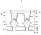
도 1 내지 도 6을 참조하여, 본 발명의 제1 실시예에 따른 반도체 장치에 대해 설명한다.1 to 6, a semiconductor device according to a first embodiment of the present invention will be described.
도 1은 본 발명의 제1 실시예에 따른 반도체 장치를 설명하기 위한 레이아웃도이다. 도 2는 도 1의 A - A를 따라서 절단한 단면도이다. 도 3은 도 1의 B - B를 따라서 절단한 단면도이다. 도 4는 도 1의 C - C를 따라서 절단한 단면도이다. 도 5는 도 4에서 제1 컨택을 제외하고 도시한 도면이다. 도 6은 도 1의 D - D를 따라서 절단한 단면도이다.1 is a layout diagram for explaining a semiconductor device according to a first embodiment of the present invention. 2 is a cross-sectional view taken along line A-A in Fig. 3 is a cross-sectional view taken along line B-B in Fig. 4 is a cross-sectional view taken along line C-C in Fig. FIG. 5 is a view showing the first contact in FIG. 4; FIG. 6 is a cross-sectional view taken along the line D-D in Fig.
도 1 내지 도 6을 참고하면, 본 발명의 제1 실시예에 따른 반도체 장치(1)는 제1 활성 영역(110)과, 제2 활성 영역(120)과, 게이트 전극(200)과, 제1 소오스/드레인(115)과, 제2 소오스/드레인(125)과, 제1 컨택(150) 등을 포함할 수 있다.1 to 6, a
제1 활성 영역(110)과 제2 활성 영역(120)은 필드 절연막(105)에 의해 정의될 수 있다. 제1 활성 영역(110) 및 제2 활성 영역(120)은 서로 간에 이격되어 배치될 수 있다.The first
제1 활성 영역(110) 및 제2 활성 영역(120)은 예를 들어, 제1 방향(X)으로 연장되어 있을 수 있다. 제1 활성 영역(110) 및 제2 활성 영역(120)은 제2 방향(Y)으로 배열되어 있을 수 있다.The first
제1 활성 영역(110)과 제2 활성 영역(120) 사이에는 필드 절연막(105)이 배치될 수 있다. 본 발명의 실시예들에 따른 반도체 장치에서, 제1 활성 영역(110) 및 제2 활성 영역(120)은 최인접하고 있을 수 있다. 즉, 제1 활성 영역(110)과 제2 활성 영역(120) 사이에 필드 절연막(105)이 배치되고, 다른 활성 영역은 배치되지 않을 수 있다.A
제1 활성 영역(110) 및 제2 활성 영역(120)은 각각 단채널 활성 영역이거나, 다채널 활성 영역 중 하나일 수 있다. 본 발명의 제1 실시예에 따른 반도체 장치(1)에서, 제1 활성 영역(110) 및 제2 활성 영역(120)은 기판(100)으로부터 돌출되어 있는 핀형 액티브 패턴인 것으로 설명한다.The first
필드 절연막(105)은 제1 활성 영역(110) 및 제2 활성 영역(120)의 측벽의 일부를 덮고 있기 때문에, 제1 활성 영역(110) 및 제2 활성 영역(120)의 적어도 일부는 각각 필드 절연막(105)보다 위로 돌출되어 있을 수 있다. 즉, 제1 활성 영역(110)의 상면 및 제2 활성 영역(120)의 상면의 적어도 일부는 각각 필드 절연막(105)의 상면보다 위로 돌출되어 있을 수 있다.Since the
기판(100)은 예를 들어, 벌크 실리콘 또는 SOI(silicon-on-insulator)일 수 있다. 이와 달리, 기판(100)은 실리콘 기판일 수도 있고, 또는 다른 물질, 예를 들어, 실리콘게르마늄, 안티몬화 인듐, 납 텔루르 화합물, 인듐 비소, 인듐 인화물, 갈륨 비소 또는 안티몬화 갈륨을 포함할 수 있다. 또는, 기판(100)은 베이스 기판 상에 에피층이 형성된 것일 수도 있다.The
필드 절연막(105)은 예를 들어, 산화막, 질화막, 산질화막 또는 이들의 조합 중 하나를 포함할 수 있지만, 이에 제한되는 것은 아니다.The
핀형 액티브 패턴인 제1 활성 영역(110) 및 제2 활성 영역(120)은 각각 기판(100)의 일부일 수도 있고, 기판(100)으로부터 성장된 에피층(epitaxial layer)을 포함할 수 있다.The first
제1 활성 영역(110) 및 제2 활성 영역(120)은 예를 들어, 원소 반도체 물질인 실리콘 또는 게르마늄을 포함할 수 있다. 또한, 제1 활성 영역(110) 및 제2 활성 영역(120)은 화합물 반도체를 포함할 수 있고, 예를 들어, IV-IV족 화합물 반도체 또는 III-V족 화합물 반도체를 포함할 수 있다.The first
IV-IV족 화합물 반도체를 예로 들면, 제1 활성 영역(110) 및 제2 활성 영역(120)은 각각 탄소(C), 규소(Si), 게르마늄(Ge), 주석(Sn) 중 적어도 2개 이상을 포함하는 이원계 화합물(binary compound), 삼원계 화합물(ternary compound) 또는 이들에 IV족 원소가 도핑된 화합물일 수 있다.For example, the first
III-V족 화합물 반도체를 예로 들면, 제1 활성 영역(110) 및 제2 활성 영역(120)은 각각 III족 원소로 알루미늄(Al), 갈륨(Ga) 및 인듐(In) 중 적어도 하나와 V족 원소인 인(P), 비소(As) 및 안티모늄(Sb) 중 하나가 결합되어 형성되는 이원계 화합물, 삼원계 화합물 또는 사원계 화합물 중 하나일 수 있다.For example, the first
본 발명의 제1 실시예에 따른 반도체 장치(1)에서, 제1 활성 영역(110) 및 제2 활성 영역(120)은 실리콘을 포함하는 실리콘 핀형 액티브 패턴인 것으로 설명한다.In the
게이트 전극(200)은 제2 방향(Y)으로 연장되어, 제1 활성 영역(110) 및 제2 활성 영역(120)과 교차하도록 형성될 수 있다. 게이트 전극(200)은 제1 활성 영역(110), 제2 활성 영역(120) 및 필드 절연막(105) 상에 형성될 수 있다.The
본 발명의 제1 실시예에 따른 반도체 장치(1)에서, 게이트 전극(200)은 금속층(MG1, MG2)을 포함할 수 있다. 게이트 전극(200)은 도시된 것과 같이, 2층 이상의 금속층(MG1, MG2)이 적층될 수 있다. 제1 금속층(MG1)은 일함수 조절을 하고, 제2 금속층(MG2)은 제1 금속층(MG1)에 의해 형성된 공간을 채우는 역할을 할 수 있다.In the
예를 들어, 제1 금속층(MG1)은 TiN, TaN, TiC, 및 TaC 중 적어도 하나를 포함할 수 있다. 또한, 제2 금속층(MG2)은 W 또는 Al을 포함할 수 있다. 또는, 게이트 전극(200)은 금속이 아닌, Si, SiGe 등으로 이루어질 수도 있다. 이러한 게이트 전극(200)은 예를 들어, 리플레이스먼트(replacement) 공정(또는 게이트 라스트 공정(gate last process))을 통해서 형성될 수 있으나, 이에 한정되는 것은 아니다.For example, the first metal layer MG1 may include at least one of TiN, TaN, TiC, and TaC. In addition, the second metal layer MG2 may include W or Al. Alternatively, the
게이트 절연막(210)은 제1 활성 영역(110)과 게이트 전극(200) 사이, 및 제2 활성 영역(120)과 게이트 전극(200) 사이에 형성될 수 있다. 게이트 절연막(210)은 필드 절연막(105)보다 위로 돌출된 제1 활성 영역(110)의 측벽 및 상면과, 제2 활성 영역(120)의 측벽 및 상면을 따라서 형성될 수 있다. 또한, 게이트 절연막(210)은 게이트 전극(200)과 필드 절연막(105) 사이에 배치될 수 있다.A
게이트 절연막(210)은 예를 들어, 실리콘 산화막, 실리콘 산질화막, 실리콘 질화막, 게르마늄 산질화막(GeON), 실리콘 게르마늄 산화막(GeSiO) 또는 고유전율 물질을 포함할 수 있다. 고유전율 물질은 예를 들어, 하프늄 산화물(hafnium oxide), 하프늄 실리콘 산화물(hafnium silicon oxide), 란타늄 산화물(lanthanum oxide), 란타늄 알루미늄 산화물(lanthanum aluminum oxide), 지르코늄 산화물(zirconium oxide), 지르코늄 실리콘 산화물(zirconium silicon oxide), 탄탈륨 산화물(tantalum oxide), 티타늄 산화물(titanium oxide), 바륨 스트론튬 티타늄 산화물(barium strontium titanium oxide), 바륨 티타늄 산화물(barium titanium oxide), 스트론튬 티타늄 산화물(strontium titanium oxide), 이트륨 산화물(yttrium oxide), 알루미늄 산화물(Aluminum oxide), 납 스칸듐 탄탈륨 산화물(lead scandium tantalum oxide), 또는 납 아연 니오브산염(lead zinc niobate) 중에서 하나 이상을 포함할 수 있으나, 이에 제한되는 것은 아니다.The
게이트 스페이서(220)은 제2 방향(Y)으로 연장된 게이트 전극(200)의 측벽 상에 형성될 수 있다. 게이트 스페이서(220)는 예를 들어, 실리콘 질화물(SiN), 실리콘 산질화물(SiON), 실리콘 산화물(SiO2), 실리콘 산탄질화물(SiOCN) 및 이들의 조합 중 적어도 하나를 포함할 수 있다. 게이트 스페이서(220)는 단일막으로 도시되었지만, 이에 제한되는 것은 아니며, 다중막의 구조를 가질 수 있음은 물론이다.The
제1 소오스/드레인(115)은 게이트 전극(200)의 양측에 형성될 수 있다. 제1 소오스/드레인(115)은 제1 활성 영역(110)과 중첩되도록 형성될 수 있다. 제1 소오스/드레인(115)은 상승된 소오스/드레인일 수 있다.The first source /
제2 소오스/드레인(125)은 게이트 전극(200)의 양측에 형성될 수 있다. 제2 소오스/드레인(125)은 제2 활성 영역(120)과 중첩되도록 형성될 수 있다. 제2 소오스/드레인(125)은 상승된 소오스/드레인일 수 있다.The second source /
제1 소오스/드레인(115) 및 제2 소오스/드레인(125)은 서로 간에 인접하여 형성되지만, 서로 이격되어 있을 수 있다. 제1 소오스/드레인(115) 및 제2 소오스/드레인(125)은 서로 접촉하지 않을 수 있다. 즉, 게이트 전극(200)을 중심으로, 게이트 전극(200)의 일측에 배치되는 제1 소오스/드레인(115) 및 제2 소오스/드레인(125)은 서로 간에 이격되어 있을 수 있다.The first source /
본 발명의 제1 실시예에 따른 반도체 장치(1)에서, 제1 소오스/드레인(115)은 제1 활성 영역(110) 상에 형성될 수 있고, 제2 소오스/드레인(125)은 제2 활성 영역(120) 상에 형성될 수 있다.In the
도 2 및 도 4에서, 제1 소오스/드레인(115)의 일부는 제1 활성 영역(110) 내에 형성된 리세스를 채우도록 형성되고, 제2 소오스/드레인(125)의 일부는 제2 활성 영역(120) 내에 형성된 리세스를 채우도록 형성되는 것으로 도시되었지만, 이에 제한되는 것은 아니다.2 and 4, a portion of the first source /
즉, 제1 소오스/드레인(115)은 필드 절연막(105)보다 위로 돌출된 제1 활성 영역(110)의 적어도 일부를 덮는 에피층을 포함할 수도 있다. 제2 소오스/드레인(125)도 제1 소오스/드레인(115)과 마찬가지일 수 있다.That is, the first source /
본 발명의 제1 실시예에 따른 반도체 장치(1)가 PMOS 트랜지스터인 경우, 제1 소오스/드레인(115) 및 제2 소오스/드레인(125)은 각각 압축 스트레스 물질을 포함할 수 있다. 예를 들어, 압축 스트레스 물질은 Si에 비해서 격자상수가 큰 물질일 수 있고, 예를 들어 SiGe일 수 있다. 압축 스트레스 물질은 제1 활성 영역(110) 및 제2 활성 영역(120)에 각각 압축 스트레스를 가하여 채널 영역의 캐리어의 이동도(mobility)를 향상시킬 수 있다.When the
이와는 달리, 반도체 장치(1)가 NMOS 트랜지스터인 경우, 제1 소오스/드레인(115) 및 제2 소오스/드레인(125)은 각각 제1 활성 영역(110) 및 제2 활성 영역(120)과 동일 물질 또는, 인장 스트레스 물질일 수 있다. 예를 들어, 제1 활성 영역(110) 및 제2 활성 영역(120)이 실리콘 핀형 액티브 패턴일 때, 제1 소오스/드레인(115) 및 제2 소오스/드레인(125)은 Si이거나, Si보다 격자 상수가 작은 물질(예를 들어, SiC 또는 탄소를 포함하는 실리콘(Si:C))일 수 있다.In contrast, when the
식각 정지막(185)는 제1 소오스/드레인(115) 및 제2 소오스/드레인(125) 상에 형성될 수 있다. 식각 정지막(185)은 제1 소오스/드레인(115) 및 제2 소오스/드레인(125)의 외주면과, 필드 절연막(105)의 상면을 따라서 형성될 수 있다.The
식각 정지막(185)은 예를 들어, 실리콘 질화물(SiN), 실리콘 산질화물(SiON), 실리콘 산화물(SiO2), 실리콘 산탄질화물(SiOCN), 실리콘 탄질화물(SiCN) 및 이들의 조합 중 적어도 하나를 포함할 수 있다.
층간 절연막(180)은 게이트 전극(200)과, 제1 소오스/드레인(115)과, 제2 소오스/드레인(125)을 덮을 수 있다. 층간 절연막(180)은 식각 정지막(185) 상에 형성될 수 있다.The interlayer insulating
층간 절연막(180)은 하부 층간 절연막(181)과 상부 층간 절연막(182)을 포함할 수 있다. 하부 층간 절연막(181)과 상부 층간 절연막(182)은 예를 들어, 게이트 전극(200)을 형성하기 전에 증착되는지 여부로 구분될 수 있지만, 이에 제한되는 것은 아니다.The interlayer insulating
층간 절연막(180)은 예를 들어, 실리콘 산화물, 실리콘 질화물, 실리콘 산질화물 및 실리콘 산화물보다 유전율이 낮은 저유전율 물질 중 적어도 하나를 포함할 수 있다. 저유전율 물질은 예를 들어, FOX(Flowable Oxide), TOSZ(Torene SilaZene), USG(Undoped Silica Glass), BSG(Borosilica Glass), PSG(PhosphoSilaca Glass), BPSG(BoroPhosphoSilica Glass), PETEOS(Plasma Enhanced Tetra Ethyl Ortho Silicate), FSG(Fluoride Silicate Glass), CDO(Carbon Doped silicon Oxide), Xerogel, Aerogel, Amorphous Fluorinated Carbon, OSG(Organo Silicate Glass), Parylene, BCB(bis-benzocyclobutenes), SiLK, polyimide, porous polymeric material 또는 이들의 조합을 포함할 수 있으나, 이에 제한되는 것은 아니다.The
층간 절연막(180)은 제1 컨택홀(155)과 제2 컨택홀(255)을 포함할 수 있다. 제2 컨택홀(255)은 게이트 전극(200) 상에 형성되어, 게이트 전극(200)의 상면을 노출시킬 수 있다.The interlayer insulating
제1 컨택홀(155)은 제1 소오스/드레인(115) 및 제2 소오스/드레인(125) 상에 형성될 수 있다. 제1 컨택홀(155)에 의해, 제1 소오스/드레인의 상면(115u) 및 제2 소오스/드레인의 상면(125u)은 동시에 노출될 수 있다. 즉, 게이트 전극(200)의 일측 및 타측에서, 제1 컨택홀(155)은 제2 방향(Y)으로 연장될 수 있다.The
제1 컨택(150)은 층간 절연막(180) 내에 형성될 수 있다. 제1 컨택(150)은 제1 컨택홀(155)을 채워서 형성될 수 있다. 제1 컨택(150)은 제1 소오스/드레인(115) 및 제2 소오스/드레인(125)과 연결될 수 있다. 다시 말하면, 제1 컨택(150)은 제1 소오스/드레인(115) 및 제2 소오스/드레인(125)의 공통된 컨택일 수 있다.The
본 발명의 제1 실시예에 따른 반도체 장치(1)에서, 제1 컨택(150)의 일부는 제1 소오스/드레인(115) 및 제2 소오스/드레인(125)에 의해 감싸일 수 있다.In the
도 2에서 도시된 것과 같이, 제1 소오스/드레인의 상면(115u)의 적어도 일부 및 제2 소오스/드레인(125)의 상면의 적어도 일부는 식각되어, 제1 소오스/드레인(115) 및 제2 소오스/드레인(125) 내에 리세스가 형성될 수 있다. 제1 컨택(150)의 일부는 제1 소오스/드레인(115) 및 제2 소오스/드레인(125) 내에 리세스에 형성되므로, 제1 컨택(150)의 일부는 제1 소오스/드레인(115) 및 제2 소오스/드레인(125)에 의해 감싸일 수 있다.At least a portion of the
제1 컨택(150)은 게이트 전극(200)의 일측에 형성된 제1 소오스/드레인(115) 및 제2 소오스/드레인(125)과 동시에 연결되므로, 제1 컨택(150)은 제2 방향(Y)으로 연장되어 있을 수 있다.The
제1 컨택(150)은 제1 배리어막(151)과 제1 필링막(152)을 포함할 수 있다. 제1 배리어막(151)은 제1 컨택홀(155)을 따라서 형성될 수 있다.The
제1 필링막(152)은 제1 배리어막(151)이 형성된 제1 컨택홀(155)을 채울 수 있다. 제1 필링막(152)은 제1 배리어막(151) 상에 형성될 수 있다.The
제2 컨택(250)은 층간 절연막(180) 내에 형성될 수 있다. 제2 컨택(250)은 제2 컨택홀(255)을 채워서 형성될 수 있다. 제2 컨택(250)은 게이트 전극(200)과 연결될 수 있다.The
도 1에서, 제2 컨택(250)은 게이트 전극(200)의 종단 부분에 배치되는 것으로 도시하였지만, 설명의 편의를 위한 것일 뿐, 이에 제한되는 것은 아니다.1, the
제2 컨택(250)은 제2 배리어막(251)과 제2 필링막(252)을 포함할 수 있다. 제2 배리어막(251)은 제2 컨택홀(255)을 따라서 형성될 수 있다.The
제2 필링막(252)은 제2 배리어막(251)이 형성된 제2 컨택홀(255)을 채울 수 있다. 제2 필링막(252)은 제2 배리어막(251) 상에 형성될 수 있다.The
제1 배리어막(151) 및 제2 배리어막(251)은 각각 예를 들어, 탄탈륨(Ta), 탄탈륨 질화물(TaN), 티타늄(Ti), 티타늄 질화물(TiN), 루테늄(Ru), 코발트(Co), 니켈(Ni), 니켈 붕화물(NiB), 또는 텅스텐 질화물(WN) 등을 포함할 수 있다.The
제1 컨택(150) 및 제2 컨택(250)은 각각 예를 들어, 알루미늄(Al), 텅스텐(W), 구리(Cu), 코발트(Co) 또는 도핑된 폴리실리콘 등을 포함할 수 있다.The
도 1, 도 4 내지 도 6에서, 제1 컨택(150)은 제1 컨택의 제1 부분(150a)과, 제1 컨택의 제2 부분(150b)과, 제1 컨택의 연결 부분(150c)을 포함할 수 있다.1, 4 to 6, the
제1 컨택의 연결 부분(150c)은 제1 컨택의 제1 부분(150a)과 제1 컨택의 제2 부분(150b) 사이에 배치될 수 있다. 즉, 제1 컨택의 제1 부분(150a) 및 제1 컨택의 제2 부분(150b)은 제1 컨택의 연결 부분(150c)을 중심으로 제2 방향(Y)으로 배치될 수 있다.The connecting
제1 컨택의 제1 부분(150a)은 제1 소오스/드레인(115) 상에 배치될 수 있다. 제1 컨택의 제1 부분(150a)은 제1 소오스/드레인(115)과 오버랩되지만, 제2 소오스/드레인(125)과 오버랩되지 않을 수 있다. 제1 컨택의 제1 부분(150a)은 한번의 제조 공정에 의해 형성되는 통합 구조(integral structure)일 수 있다.The
제1 컨택의 제2 부분(150b)은 제2 소오스/드레인(125) 상에 배치될 수 있다. 제1 컨택의 제2 부분(150b)은 제2 소오스/드레인(125)과 오버랩되지만, 제1 소오스/드레인(115)과 오버랩되지 않을 수 있다. 제1 컨택의 제2 부분(150b)은 한번의 제조 공정에 의해 형성되는 통합 구조(integral structure)일 수 있다.The
제1 컨택의 연결 부분(150c)은 제1 컨택의 제1 부분(150a)과 제1 컨택의 제2 부분(150b)을 연결할 수 있다. 제1 컨택의 연결 부분(150c)은 게이트 전극(200)의 일측에 배치되는 제1 소오스/드레인(115) 및 제2 소오스/드레인(125) 사이에 배치될 수 있다.The connecting
제1 컨택의 제1 부분(150a)의 상면과, 제1 컨택의 제2 부분(150b)의 상면과, 제1 컨택의 연결 부분(150c)의 상면은 동일 평면 상에 놓여있을 수 있다. 즉, 제1 컨택(150)의 상면은 동일 평면 상에 놓여 있을 수 있다.The upper surface of the
도 4에서, 제1 컨택의 제1 부분(150a)의 상면 및 상부 층간 절연막(182)의 상면 사이의 경계와, 제1 컨택의 제2 부분(150b)의 상면 및 상부 층간 절연막(182)의 상면 사이의 경계가 연속적인 것으로 도시되었지만, 이에 제한되는 것은 아니다.A boundary between the upper surface of the
제1 컨택의 제1 부분(150a)의 높이(h1)는 제1 컨택의 연결 부분(150c)의 높이(h3)와 다르고, 제1 컨택의 제2 부분(150b)의 높이(h2)는 제1 컨택의 연결 부분(150c)의 높이(h3)와 다를 수 있다.The height h1 of the
도 4에서, 제1 컨택의 제1 부분(150a)의 높이(h1)는 제1 컨택의 제2 부분(150b)의 높이(h2)와 실질적으로 동일한 것으로 도시하였지만, 설명의 편의성을 위한 것일 뿐, 이에 제한되는 것은 아니다. 즉, 제1 컨택홀(155)을 형성하는 과정에서의 공정 마진에 따라, 제1 컨택의 제1 부분(150a)의 높이(h1)와 제1 컨택의 제2 부분(150b)의 높이(h2)는 다소 차이가 있을 수 있음은 물론이다.4, the height h1 of the
본 발명의 제1 실시예에 따른 반도체 장치(1)에서, 제1 컨택의 제1 부분(150a)의 높이(h1)는 제1 컨택의 연결 부분(150c)의 높이(h3)보다 높을 수 있다. 또한, 제1 컨택의 제2 부분(150b)의 높이(h2)는 제1 컨택의 연결 부분(150c)의 높이(h3)보다 높을 수 있다.In the
또는, 층간 절연막(180)의 상면을 기준으로, 제1 컨택의 제1 부분(150a)의 바닥면 및 제1 컨택의 제2 부분(150b)의 바닥면은 제1 컨택의 연결 부분(150c)의 바닥면보다 깊을 수 있다. 반대로, 필드 절연막(105)의 상면을 기준으로, 제1 컨택의 제1 부분(150a)의 바닥면 및 제1 컨택의 제2 부분(150b)의 바닥면은 제1 컨택의 연결 부분(150c)의 바닥면보다 낮을 수 있다.Alternatively, the bottom surface of the
덧붙여, 층간 절연막(180)의 상면을 기준으로, 제1 컨택의 연결 부분(150c)의 바닥면은 제1 소오스/드레인의 상면(115u) 및 제2 소오스/드레인의 상면(125u)보다 얕을 수 있다.The bottom surface of the connecting
제1 컨택의 연결 부분(150c)의 높이(h3)는 제2 컨택(250)의 높이와 실질적으로 동일할 수 있지만, 이에 제한되는 것은 아니다. 여기서, "높이가 동일하다"의 의미는 비교되는 2개의 높이가 완전히 동일한 것뿐만 아니라, 공정 과정상의 마진 등으로 인해서 발생할 수 있는 미세한 높이의 차이를 포함하는 의미이다.The height h3 of the connecting
다시 말하면, 게이트 전극(200)의 상면으로부터 층간 절연막(180)의 상면까지의 높이는 제1 컨택의 연결 부분(150c)의 높이(h3)와 실질적으로 동일할 수 있다.In other words, the height from the top surface of the
또는, 제1 컨택의 연결 부분(150c)의 높이(h3)는 상부 층간 절연막(182)의 두께와 실질적으로 동일할 수 있지만, 이에 제한되는 것은 아니다. 게이트 전극(200)의 상면에 캡핑 패턴이 형성됨으로써, 게이트 전극(200)의 상면이 게이트 스페이서(220)의 상면보다 리세스되어 있을 경우, 제1 컨택의 연결 부분(150c)의 높이(h3)는 상부 층간 절연막(182)의 두께보다 클 수 있다.Alternatively, the height h3 of the connecting
제1 컨택의 연결 부분(150c)의 높이(h3)는 제2 컨택(250)의 높이와 실질적으로 동일할 수 있으므로, 기판(100)의 두께 방향으로 제1 컨택의 연결 부분(150c)은 게이트 전극(200)과 오버랩되지 않을 수 있다.The height h3 of the connecting
이를 통해, 제1 컨택의 연결 부분(150c)과 게이트 전극(200) 사이의 캐패시턴스를 감소시킬 수 있다. 다시 말하면, 제1 컨택(150)과 게이트 전극(200) 사이의 유효 캐패시턴스가 감소함에 따라, 제1 컨택(150)과 게이트 전극(200) 사이의 커플링 현상을 경감시킬 수 있고, 이를 통해 반도체 장치의 신뢰성 및 성능을 개선할 수 있다.Thus, the capacitance between the
제1 컨택홀(155)은 제1 트렌치(155a)와, 제2 트렌치(155b)와, 연결 트렌치(155c)를 포함할 수 있다. 연결 트렌치(155c)는 제1 트렌치(155a)와 제2 트렌치(155b) 사이에 형성될 수 있다.The
제1 트렌치(155a)는 제1 컨택의 제1 부분(150a)에 대응되고, 제2 트렌치(155b)는 제1 컨택의 제2 부분(150b)에 대응될 수 있다. 또한, 연결 트렌치(155c)는 제1 컨택의 연결 부분(150c)에 대응될 수 있다.The
제1 컨택홀(155)은 측면(155s)과, 측면(155s)을 연결하는 바닥면(155L)을 포함할 수 있다. 좀 더 구체적으로, 제1 컨택홀의 측면(155S)은 도 1에서의 제1 컨택(150)의 외주면을 따라서 형성되는 부분이고, 제1 컨택홀의 바닥면(155L)은 제1 컨택홀의 측면(155S)을 연결하는 부분일 수 있다.The
제1 트렌치(155a)의 바닥면은 제1 컨택의 제1 부분(150a)의 바닥면에 대응되고, 제2 트렌치(155b)의 바닥면은 제1 컨택의 제2 부분(150b)의 바닥면에 대응되고, 연결 트렌치(155c)의 바닥면은 제1 컨택의 연결 부분(150c)에 대응될 수 있다.The bottom surface of the
층간 절연막(180)의 상면을 기준으로, 제1 컨택의 제1 부분(150a)의 바닥면 및 제1 컨택의 제2 부분(150b)의 바닥면은 제1 컨택의 연결 부분(150c)의 바닥면보다 깊다.The bottom surface of the
따라서, 층간 절연막(180)의 상면을 기준으로, 제1 트렌치(155a)의 바닥면 및 제2 트렌치(155b)의 바닥면은 연결 트렌치(155c)의 바닥면보다 깊게 형성될 수 있다. 즉, 제1 컨택홀의 바닥면(155L)은 제1 컨택(150)의 바닥면에 대응되어 굴곡진 바닥면일 수 있다.The bottom surface of the
또한, 게이트 전극(200)의 상면으로부터 층간 절연막(180)의 상면까지의 높이는 제1 컨택의 연결 부분(150c)의 높이(h3)와 실질적으로 동일할 수 있으므로, 연결 트렌치(155c)의 바닥면은 하부 층간 절연막(181)과 상부 층간 절연막(182)의 경계면일 수 있지만, 이에 제한되는 것은 아니다.Since the height from the top surface of the
제1 배리어막(151)은 제1 컨택홀의 측면(155S) 및 제1 컨택홀의 바닥면(155L)을 따라서 형성될 수 있다. 또한, 제1 필링막(152)은 제1 배리어막(151) 상에 형성되고, 제1 컨택홀(155)을 채울 수 있다.The
본 발명의 제1 실시예에 따른 반도체 장치(1)에서, 제1 필링막(152)은 제1 배리어막(151)에 의해 구획되지 않을 수 있다. 다시 말하면, 제1 배리어막(151)은 제1 컨택홀의 바닥면(155L)으로부터 돌출되는 돌출부를 포함하지 않을 수 있다.In the
따라서, 제1 컨택의 제1 부분(150a)에 포함되는 제1 필링막과, 제1 컨택의 제2 부분(150b)에 포함되는 제1 필링막과, 제1 컨택의 연결 부분(150c)에 포함되는 제1 필링막은 서로 직접 연결되는 통합 구조(integral structure)일 수 있다.Therefore, the first peeling film included in the
도 7은 본 발명의 제2 실시예에 따른 반도체 장치를 설명하기 위한 도면이다. 설명의 편의상, 도 1 내지 도 6을 이용하여 설명한 실시예와 다른 점을 위주로 설명한다. 참고적으로, 도 7은 도 1의 C - C를 따라서 절단한 단면도일 수 있다.7 is a view for explaining a semiconductor device according to a second embodiment of the present invention. For convenience of explanation, the differences from the embodiments described with reference to Figs. 1 to 6 will be mainly described. For reference, FIG. 7 may be a sectional view cut along the line C - C in FIG.
도 7을 참고하면, 본 발명의 제2 실시예에 따른 반도체 장치(2)에서, 제1 배리어막(151)은 제1 컨택홀의 바닥면(155L)으로부터 돌출되는 돌출부(151p)를 더 포함할 수 있다.7, in the
제1 배리어막의 돌출부(151p)는 제1 컨택홀의 바닥면(155L)을 따라서 형성된 제1 배리어막(151)으로부터 돌출될 수 있다.The
제1 배리어막의 돌출부(151p)는 제1 컨택홀의 바닥면(155L)으로부터 돌출되어, 제1 컨택(150)의 상면까지 연장될 수 있다. 이에 따라, 제1 필링막(152)은 제1 배리어막의 돌출부(151p)에 의해 적어도 2개 영역으로 구획될 수 있다.The
즉, 제1 컨택의 제1 부분(150a)에 포함되는 제1 필링막과, 제1 컨택의 제2 부분(150b)에 포함되는 제1 필링막과, 제1 컨택의 연결 부분(150c)에 포함되는 제1 필링막 중 적어도 두 개는 제1 배리어막의 돌출부(151p)에 의해 구획될 수 있다.That is, the first peeling film included in the
따라서, 제1 컨택의 제1 부분(150a)에 포함되는 제1 필링막과, 제1 컨택의 제2 부분(150b)에 포함되는 제1 필링막과, 제1 컨택의 연결 부분(150c)에 포함되는 제1 필링막 중 적어도 두 개는 서로 직접 연결되지 않을 수 있다.Therefore, the first peeling film included in the
또한, 제1 배리어막의 돌출부(151p)의 두께는 제1 컨택홀의 측면(155S)을 따라서 형성되는 제1 배리어막(151)의 두께보다 두꺼울 수 있다. 제1 컨택홀의 측면(155S)을 따라서 형성되는 제1 배리어막(151)과 달리, 제1 배리어막의 돌출부(151p)는 두 번의 증착 과정을 통해서 형성될 수 있기 때문이다.The thickness of the
도 7에서, 제1 컨택(150)의 상면은 동일 평면 상에 놓여있는 있는 것으로 도시되어 있다. 즉, 제1 컨택의 제1 부분(150a)의 상면과, 제1 컨택의 제2 부분(150b)의 상면과, 제1 컨택의 연결 부분(150c)의 상면은 동일 평면 상에 놓여있는 것으로 도시하였지만, 설명의 편의성을 위한 것일 뿐, 이에 제한되는 것은 아니다.In Figure 7, the top surface of the
예를 들어, 도 7에서 도시된 것과 달리, 제1 컨택의 제1 부분(150a)의 상면 및 제1 배리어막의 돌출부(151p)의 상면 사이의 경계가 불연속적일 수도 있음은 물론이다.For example, it is needless to say that the boundary between the upper surface of the
도 8은 본 발명의 제3 실시예에 따른 반도체 장치를 설명하기 위한 도면이다. 설명의 편의상, 도 7을 이용하여 설명한 실시예와 다른 점을 위주로 설명한다. 참고적으로, 도 8은 도 1의 C - C를 따라서 절단한 단면도일 수 있다.8 is a view for explaining a semiconductor device according to a third embodiment of the present invention. For convenience of explanation, differences from the embodiment described with reference to Fig. 7 will be mainly described. For reference, Fig. 8 may be a sectional view cut along the line C-C in Fig.
도 8을 참고하면, 본 발명의 제3 실시예에 따른 반도체 장치(3)에서, 제1 배리어막(151)은 제1 컨택홀의 바닥면(155L)으로부터 돌출되고, 상부(151p-1)와 하부(151p-2)를 포함하는 돌출부(151p)를 더 포함할 수 있다.8, in the
제1 배리어막의 돌출부(151p)는 제1 컨택홀의 바닥면(155L)을 따라서 형성된 제1 배리어막(151)으로부터 돌출되는 하부(151p-2)와, 제1 배리어막의 돌출부의 하부(151p-2) 상에 형성되는 상부(151p-1)를 포함할 수 있다.The
제1 배리어막의 돌출부의 하부(151p-2)의 두께는 제1 배리어막의 돌출부의 상부(151p-1)의 두께와 다를 수 있다. 좀 더 구체적으로, 제1 배리어막의 돌출부의 하부(151p-2)와 제1 배리어막의 돌출부의 상부(151p-1)의 경계에서, 제1 배리어막의 돌출부(151p)의 두께의 불연속함이 있을 수 있다.The thickness of the
본 발명의 제3 실시예에 따른 반도체 장치(3)에서, 제1 배리어막의 돌출부의 상부(151p-1)의 두께는 제1 배리어막의 돌출부의 하부(151p-2)의 두께보다 얇을 수 있다.In the
도 9 및 도 10은 본 발명의 제4 실시예에 따른 반도체 장치를 설명하기 위한 도면들이다. 설명의 편의상, 도 1 내지 도 6을 이용하여 설명한 실시예와 다른 점을 위주로 설명한다. 참고적으로 도 9는 도 1의 C - C를 따라서 절단한 단면도이고, 도 10은 도 1의 D - D를 따라서 절단한 단면도이다.9 and 10 are views for explaining a semiconductor device according to a fourth embodiment of the present invention. For convenience of explanation, the differences from the embodiments described with reference to Figs. 1 to 6 will be mainly described. 9 is a sectional view taken along line C - C in FIG. 1, and FIG. 10 is a sectional view taken along line D - D in FIG.
도 9 및 도 10을 참고하면, 본 발명의 제4 실시예에 따른 반도체 장치(4)에서, 제1 컨택의 연결 부분(150c)의 높이는 제1 컨택의 제1 부분(150a)의 높이 및 제1 컨택의 제2 부분(150b)의 높이보다 높을 수 있다.9 and 10, in the
제1 컨택의 연결 부분(150c)의 높이는 제1 소오스/드레인(115)과 오버랩되는 제1 컨택의 제1 부분(150a)의 높이 및 제2 소오스/드레인(125)과 오버랩되는 제1 컨택의 제2 부분(150b)의 높이보다 높으므로, 제1 컨택의 연결 부분(150c)의 일부는 제1 소오스/드레인(115) 및 제2 소오스/드레인(125) 사이를 통과할 수 있다.The height of the
다만, 제1 컨택(150)은 필드 절연막(105)과 접촉하지 않으므로, 제1 컨택의 연결 부분(150c)과 필드 절연막(105) 사이에 층간 절연막(180)이 배치될 수 있다. 기판(100)을 기준으로, 제1 컨택의 연결 부분(150c)의 바닥면은 필드 절연막(105)의 상면보다 높을 수 있다.However, since the
층간 절연막(180)의 상면을 기준으로, 제1 컨택의 제1 부분(150a)의 바닥면 및 제1 컨택의 제2 부분(150b)의 바닥면은 제1 컨택의 연결 부분(150c)의 바닥면보다 얕을 수 있다.The bottom surface of the
반대로, 필드 절연막(105)의 상면을 기준으로, 제1 컨택의 제1 부분(150a)의 바닥면 및 제1 컨택의 제2 부분(150b)의 바닥면은 제1 컨택의 연결 부분(150c)의 바닥면보다 높을 수 있다. 다시 말하면, 필드 절연막(105)의 상면을 기준으로, 제1 소오스/드레인의 상면 및 제2 소오스/드레인의 상면(125u)은 제1 컨택의 연결 부분(150c)의 바닥면보다 높을 수 있다.Conversely, with respect to the upper surface of the
덧붙여, 제1 컨택의 연결 부분(150c)의 높이는 제2 컨택(250)의 높이보다 높을 수 있다. 이에 따라, 기판(100)의 두께 방향으로 제1 컨택의 연결 부분(150c)의 일부는 게이트 전극(200)과 오버랩될 수 있다.In addition, the height of the connecting
도 11은 본 발명의 제5 실시예에 따른 반도체 장치를 설명하기 위한 도면이다. 도 12 및 도 13은 본 발명의 제6 실시예에 다른 반도체 장치를 설명하기 위한 도면들이다. 설명의 편의상, 도 1 내지 도 6을 이용하여 설명한 실시예와 다른 점을 위주로 설명한다.11 is a view for explaining a semiconductor device according to a fifth embodiment of the present invention. 12 and 13 are views for explaining a semiconductor device according to the sixth embodiment of the present invention. For convenience of explanation, the differences from the embodiments described with reference to Figs. 1 to 6 will be mainly described.
참고적으로, 도 11은 도 1의 C - C를 따라서 절단한 단면도일 수 있다. 도 12는 도 1의 A - A를 따라서 절단한 단면도이고, 도 13은 도 1의 B - B를 따라서 절단한 단면도이다.For reference, Fig. 11 may be a sectional view cut along the line C-C in Fig. Fig. 12 is a sectional view taken along line A-A in Fig. 1, and Fig. 13 is a sectional view taken along line B-B in Fig.
도 11을 참고하면, 본 발명의 제5 실시예에 다른 반도체 장치(5)에서, 제1 소오스/드레인의 상면(115u) 및 제2 소오스/드레인의 상면(125u)은 식각되지 않아, 제1 소오스/드레인의 상면(115u) 및 제2 소오스/드레인의 상면(125u)은 전체적으로 제1 및 제2 소오스/드레인(115, 125) 형성시에 나타나는 패싯(facet)을 포함할 수 있다.11, in the
즉, 제1 컨택(150)의 바닥면의 일부는 제1 및 제2 소오스/드레인(115, 125) 형성시에 나타나는 패싯을 따라서 형성될 수 있다.That is, a portion of the bottom surface of the
도 12 및 도 13을 참고하면, 본 발명의 제6 실시예에 따른 반도체 장치(6)에서, 제1 활성 영역(110)의 상면 및 제2 활성 영역(120)의 상면은 필드 절연막(105)의 상면보다 위로 돌출되지 않을 수 있다.12 and 13, in the
게이트 전극(200)과 제1 활성 영역(110) 사이에 형성되는 게이트 절연막(210)은 필드 절연막(105)의 상면보다 위로 돌출되지 않을 수 있다.The
또한, 게이트 절연막(210)은 게이트 전극(200)과 제1 활성 영역(110) 사이, 및 게이트 전극(200)과 제2 활성 영역(120) 사이에 형성되고, 게이트 전극(200)의 측벽과 게이트 스페이서(220) 사이에 형성되지 않을 수 있다.The
본 발명의 제6 실시예에 따른 반도체 장치(6)에서, 게이트 전극(200)은 TiN, TaN, W, Al, Si, SiGe 또는 금속 실리사이드 등을 포함할 수 있다.In the
또한, 게이트 하드 마스크(205)는 게이트 전극(200) 상에 형성될 수 있다. 게이트 하드 마스크(205)는 예를 들어, 실리콘 질화막, 실리콘 산화막, 실리콘 산질화막 및 이들의 조합을 포함할 수 있다.In addition, a gate
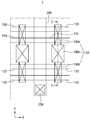
도 14는 본 발명의 제7 실시예에 따른 반도체 장치를 설명하기 위한 레이아웃도이다. 도 15는 도 14의 C - C를 따라서 절단한 단면도이다. 설명의 편의상, 도 1 내지 도 6을 이용하여 설명한 것과 다른 점을 위주로 설명한다.14 is a layout diagram for explaining a semiconductor device according to a seventh embodiment of the present invention. 15 is a sectional view cut along the line C-C in Fig. For convenience of explanation, differences from those described with reference to Figs. 1 to 6 will be mainly described.
도 14 및 도 15를 참고하면, 본 발명의 제7 실시예에 따른 반도체 장치(7)는 제3 활성 영역(130)과, 제3 소오스/드레인(135)과, 등을 더 포함할 수 있다.14 and 15, the
또한, 본 발명의 제7 실시예에 따른 반도체 장치(7)는 제4 활성 영역(140)과, 제4 소오스/드레인(145)을 더 포함할 수 있지만, 설명의 편의를 위한 것일 뿐, 이에 제한되는 것은 아니다.The
즉, 제1 컨택의 제1 부분(150a) 및 제1 컨택의 제2 부분(150b) 중 하나는 하나의 상승된 소오스/드레인과 연결될 수 있음은 물론이다.That is, one of the
제1 내지 제4 활성 영역(110, 120, 130, 140)은 제1 방향(X)으로 연장되어 있을 수 있다. 제1 내지 제4 활성 영역(110, 120, 130, 140)는 각각 서로 간에 이격되어 있을 수 있다.The first to fourth
또한, 제1 내지 제4 활성 영역(110, 120, 130, 140)은 제2 방향(Y)으로 배열되어 있을 수 있다. 제3 활성 영역(130)과, 제1 활성 영역(110)과, 제2 활성 영역(120)과, 제4 활성 영역(140)은 제2 방향(Y)으로 순차적으로 배열되어 있을 수 있다.In addition, the first to fourth
제1 활성 영역(110) 및 제2 활성 영역(120)과 같이, 필드 절연막(105)은 제3 활성 영역(130) 및 제4 활성 영역(140)의 측벽의 일부를 덮고 있을 수 있다.The
게이트 전극(200)은 제2 방향(Y)으로 연장되어, 제1 내지 제4 활성 영역(110, 120, 130, 140)과 교차하도록 형성될 수 있다. 게이트 전극(200)은 제1 내지 제4 활성 영역(110, 120, 130, 140)과 필드 절연막(105) 상에 형성될 수 있다.The
제3 소오스/드레인(135)은 게이트 전극(200)의 양측에 형성될 수 있다. 제3 소오스/드레인(135)은 제1 활성 영역(110)과 중첩되도록 형성될 수 있다. 제3 소오스/드레인(135)은 상승된 소오스/드레인일 수 있다.The third source /
제3 소오스/드레인(135)은 제1 소오스/드레인(115)과 접촉할 수 있지만, 제2 소오스/드레인(125)과 접촉하지 않을 수 있다. 좀 더 구체적으로, 게이트 전극(200)의 일측에 배치되는 제1 소오스/드레인(115) 및 제3 소오스/드레인(135)은 서로 간에 접촉할 수 있다.The third source /
제4 소오스/드레인(145)은 게이트 전극(200)의 양측에 형성될 수 있다. 제4 소오스/드레인(145)은 제4 활성 영역(140)과 중첩되도록 형성될 수 있다. 제4 소오스/드레인(145)은 상승된 소오스/드레인일 수 있다.The fourth source /
제4 소오스/드레인(145)은 제2 소오스/드레인(125)과 접촉할 수 있지만, 제1 소오스/드레인(115)과 접촉하지 않을 수 있다. 좀 더 구체적으로, 게이트 전극(200)의 일측에 배치되는 제2 소오스/드레인(125) 및 제4 소오스/드레인(145)은 서로 간에 접촉할 수 있다.The fourth source /
도 15에서 도시되는 것과 같이, 제3 소오스/드레인(135)은 제3 활성 영역(130) 상에 형성되고, 제4 소오스/드레인(145)은 제4 활성 영역(140) 상에 형성될 수 있다.A third source /
제1 컨택(150)은 제1 내지 제4 소오스/드레인(115, 125, 135, 145)과 연결될 수 있다. 다시 말하면, 제1 컨택(150)은 제1 내지 제4 소오스/드레인(115, 125, 135, 145)의 공통된 컨택일 수 있다.The
제1 컨택의 제1 부분(150a)은 서로 간에 접촉하는 제1 소오스/드레인(115) 및 제3 소오스/드레인(135) 상에 배치될 수 있다. 제1 컨택의 제1 부분(150a)은 제3 소오스/드레인(135) 상으로 연장되어 형성될 수 있다.The
제1 컨택의 제1 부분(150a)은 제1 소오스/드레인(115) 및 제3 소오스/드레인(135)과 오버랩되지만, 제4 소오스/드레인(145)과 오버랩되지 않을 수 있다.The
제1 컨택의 제2 부분(150b)은 서로 간에 접촉하는 제2 소오스/드레인(125) 및 제4 소오스/드레인(145) 상에 배치될 수 있다. 제1 컨택의 제2 부분(150b)은 제4 소오스/드레인(145) 상으로 연장되어 형성될 수 있다.The
제1 컨택의 제2 부분(150b)은 제2 소오스/드레인(125) 및 제4 소오스/드레인(145)과 오버랩되지만, 제3 소오스/드레인(135)과 오버랩되지 않을 수 있다.The
도 16은 본 발명의 제8 실시예에 따른 반도체 장치를 설명하기 위한 도면이다. 설명의 편의상, 도 14 및 도 15를 이용하여 설명한 실시예와 다른 점을 위주로 설명한다.16 is a view for explaining a semiconductor device according to an eighth embodiment of the present invention. For convenience of explanation, differences from the embodiments described with reference to Figs. 14 and 15 will be mainly described.
도 16을 참고하면, 본 발명의 제8 실시예에 따른 반도체 장치(8)에서, 제1 컨택의 연결 부분(150c)의 높이는 제1 컨택의 제1 부분(150a)의 높이 및 제1 컨택의 제2 부분(150b)의 높이보다 높을 수 있다.16, in the
필드 절연막(105)의 상면을 기준으로, 제1 컨택의 제1 부분(150a)의 바닥면 및 제1 컨택의 제2 부분(150b)의 바닥면은 제1 컨택의 연결 부분(150c)의 바닥면보다 높을 수 있다.The bottom surface of the
다시 말하면, 필드 절연막(105)의 상면을 기준으로, 제1 소오스/드레인의 상면, 제2 소오스/드레인의 상면, 제3 소오스/드레인의 상면(135u) 및 제4 소오스/드레인의 상면(145u)은 제1 컨택의 연결 부분(150c)의 바닥면보다 높을 수 있다.In other words, the upper surface of the first source / drain, the upper surface of the second source / drain, the
도 17 내지 도 24를 참조하여, 본 발명의 일 실시예에 따른 반도체 장치 제조 방법에 대해 설명한다. 본 발명의 일 실시예에 따른 반도체 장치 제조 방법을 통해, 본 발명의 제1 실시예에 따른 반도체 장치가 제조될 수 있다.A method of manufacturing a semiconductor device according to an embodiment of the present invention will be described with reference to FIGS. 17 to 24. FIG. Through the semiconductor device manufacturing method according to the embodiment of the present invention, the semiconductor device according to the first embodiment of the present invention can be manufactured.
도 17 내지 도 24는 본 발명의 일 실시예에 따른 반도체 장치 제조 방법을 설명하기 위한 중간단계 도면들이다.17 to 24 are intermediate diagrams for explaining a method of manufacturing a semiconductor device according to an embodiment of the present invention.
참고적으로, 도 18은 도 17의 E - E를 따라서 절단한 단면도이고, 도 19는 도 17의 F - F를 따라서 절단한 단면도이다.For reference, FIG. 18 is a sectional view cut along E - E in FIG. 17, and FIG. 19 is a sectional view taken along F - F in FIG.
도 17 내지 도 19를 참고하면, 서로 간에 이격되는 제1 활성 영역(110) 및 제2 활성 영역(120) 상에, 제1 활성 영역(110) 및 제2 활성 영역(120)과 교차하는 게이트 전극(200)을 형성할 수 있다.17 to 19, a first
또한, 제1 활성 영역(110)과 중첩되는 제1 소오스/드레인(115)을 게이트 전극(200)의 양측에 형성할 수 있다. 제2 활성 영역(120)과 중첩되는 제2 소오스/드레인(125)을 게이트 전극의 양측에 형성할 수 있다.Also, a first source /
이 때, 게이트 전극(200)의 일측에 형성되는 제1 소오스/드레인(115) 및 제2 소오스/드레인(125)은 서로 간에 이격되어 접촉하지 않을 수 있다.At this time, the first source /
도 17 내지 도 19에서 도시되는 것과 같이, 제1 소오스/드레인(115) 및 제2 소오스/드레인(125)을 형성한 후, 리플레이스먼트 공정을 통해 게이트 전극(200)이 형성될 수 있지만, 이에 제한되는 것은 아니다.As shown in FIGS. 17 to 19, after the first source /
이어서, 게이트 전극(200)과, 제1 소오스/드레인(115)과, 제2 소오스/드레인(125)을 덮는 층간 절연막(180)을 필드 절연막(105) 상에 형성할 수 있다.The
도 20을 참고하면, 층간 절연막(180) 내에, 제1 소오스/드레인(115)과 중첩되는 제1 트렌치(155a)와, 제2 소오스/드레인(125)과 중첩되는 제2 트렌치(155b)를 각각 형성할 수 있다.20, a
제1 트렌치(155a)는 제1 소오스/드레인(115)의 상면을 노출시키고, 제2 트렌치(155b)는 제2 소오스/드레인(125)을 노출시킬 수 있다.The
제1 트렌치(155a) 및 제2 트렌치(155b)는 층간 절연막(180)에 의해 이격되어, 서로 간에 연결되지 않을 수 있다.The
제1 트렌치(155a) 및 제2 트렌치(155b)은 식각 공정을 통해 형성될 수 있다. 제1 트렌치(155a) 및 제2 트렌치(155b)를 형성하는 식각 공정 중, 제1 소오스/드레인(115) 및 제2 소오스/드레인(125)의 상면 일부는 식각될 수 있다.The
도 21을 참고하면, 층간 절연막(180) 내에, 제1 트렌치(155a) 및 제2 트렌치(155b)를 각각 채우는 희생 패턴(156)을 형성할 수 있다.Referring to FIG. 21, a
희생 패턴(156)은 예를 들어, 갭-필 능력이 좋은 물질을 포함할 수 있다. 또한, 희생 패턴(156)은 애슁(ashing) 등의 공정을 통해 쉽게 제거되는 물질을 포함할 수 있다.The
도 22 및 도 23을 참고하면, 층간 절연막(180) 내에, 제1 트렌치(155a)와 제2 트렌치(155b)를 연결하는 연결 트렌치(155c)를 형성할 수 있다. 또한, 층간 절연막(180) 내에 게이트 전극(200)의 상면 노출시키는 제2 컨택홀(255)을 형성할 수 있다.Referring to FIGS. 22 and 23, a
연결 트렌치(155c)는 제1 트렌치(155a)와 제2 트렌치(155b) 사이에 형성될 수 있다.The
연결 트렌치(155c) 및 제2 컨택홀(255)은 식각 공정을 통해 형성될 수 있다. 연결 트렌치(155c) 및 제2 컨택홀(255)은 층간 절연막(180) 내에 동시에 형성될 수 있다.The
연결 트렌치(155c)의 측면은 제1 트렌치(155a) 및 제2 트렌치(155b)를 각각 채우고 있는 희생 패턴(156)일 수 있다.The side of the
도 24를 참고하면, 제1 트렌치(155a) 및 제2 트렌치(155b)를 각각 채우고 있는 희생 패턴(156)을 제거할 수 있다.Referring to FIG. 24, the
이를 통해, 제1 트렌치(155a)와, 제2 트렌치(155b)와, 연결 트렌치(155c)를 포함하는 제1 컨택홀(155)을 형성할 수 있다. 제1 컨택홀(155)에 의해, 제1 소오스/드레인의 상면(115u) 및 제2 소오스/드레인의 상면(125u)은 노출될 수 있다.Thus, the
이어서, 도 4를 참고하면, 제1 컨택홀(155)의 측면 및 바닥면을 따라서 형성되는 제1 배리어막(151)과, 제1 컨택홀(155)을 채우는 제1 필링막(152)을 형성함으로써, 층간 절연막(180) 내에 제1 컨택(150)을 형성할 수 있다.4, a
또한, 제2 컨택홀(255)의 측면 및 바닥면을 따라서 형성되는 제2 배리어막(251)과, 제2 컨택홀(255)을 채우는 제2 필링막(252)을 형성함으로써, 층간 절연막(180) 내에 제2 컨택(250)을 형성할 수 있다.The
제1 컨택(150)과 제2 컨택(250)은 동시에 형성될 수 있지만, 이에 제한되는 것은 아니다.The
도 17 내지 도 20, 도 25 내지 도 27을 참조하여, 본 발명의 다른 실시예에 따른 반도체 장치 제조 방법에 대해 설명한다. 본 발명의 다른 실시예에 따른 반도체 장치 제조 방법을 통해, 본 발명의 제2 실시예 또는 제3 실시예에 따른 반도체 장치가 제조될 수 있다.17 to 20, and 25 to 27, a method of manufacturing a semiconductor device according to another embodiment of the present invention will be described. The semiconductor device according to the second embodiment or the third embodiment of the present invention can be manufactured through the semiconductor device manufacturing method according to another embodiment of the present invention.
도 25 내지 도 27은 본 발명의 다른 실시예에 따른 반도체 장치 제조 방법을 설명하기 위한 중간단계 도면들이다.FIGS. 25 to 27 are intermediate diagrams for explaining a semiconductor device manufacturing method according to another embodiment of the present invention.
도 25를 참고하면, 층간 절연막(180) 내에, 제1 소오스/드레인(115)과 연결되는 제1 컨택의 제1 부분(150a)과, 제2 소오스/드레인(125)과 연결되는 제1 컨택의 제2 부분(150b)을 형성할 수 있다.25, a
제1 컨택의 제1 부분(150a)은 제1 트렌치(155a)를 채워 형성되고, 제1 컨택의 제2 부분(150b)은 제2 트렌치(155b)를 채워 형성될 수 있다.The
제1 컨택의 제1 부분(150a)과 제1 컨택의 제2 부분(150b)은 동시에 형성될 수 있다.The
도 26 및 도 27을 참고하면, 층간 절연막(180) 내에 제1 트렌치(155a)와 제2 트렌치(155b)를 연결하는 연결 트렌치(155c)를 형성할 수 있다. 연결 트렌치(155c)는 제1 컨택의 제1 부분(150a)과 제1 컨택의 제2 부분(150b)을 측면으로 가질 수 있다.Referring to FIG. 26 and FIG. 27, a
즉, 연결 트렌치(155c)는 층간 절연막(180)과, 제1 컨택의 제1 부분(150a)과, 제1 컨택의 제2 부분(150b)에 의해 정의될 수 있다.That is, the
또한, 층간 절연막(180) 내에 게이트 전극(200)의 상면 노출시키는 제2 컨택홀(255)을 형성할 수 있다.In addition, the
이어서 도 7 또는 도 8을 참고하면, 층간 절연막(180) 내에, 제1 컨택의 제1 부분(150a)과 제1 컨택의 제2 부분(150b)과 접하고, 연결 트렌치(155c)를 채우는 제1 컨택의 연결 부분(150c)을 형성할 수 있다.7 or 8, a
이를 통해, 제1 컨택의 제1 부분(150a)과 제1 컨택의 제2 부분(150b)과, 제1 컨택의 연결 부분(150c)을 포함하는 제1 컨택(150)을 층간 절연막(180) 내에 형성할 수 있다.The
또한, 제2 컨택홀(255)을 채우는 제2 컨택(250)을 층간 절연막(180) 내에 형성할 수 있다.In addition, the
제1 컨택의 연결 부분(150c)과, 제2 컨택(250)은 동시에 형성될 수 있지만, 이에 제한되는 것은 아니다.The
도 28은 본 발명의 몇몇 실시예에 따른 반도체 장치를 포함하는 전자 시스템의 블록도이다.28 is a block diagram of an electronic system including a semiconductor device according to some embodiments of the present invention.
도 28을 참조하면, 본 발명의 실시예에 따른 전자 시스템(1100)은 컨트롤러(1110), 입출력 장치(1120, I/O), 기억 장치(1130, memory device), 인터페이스(1140) 및 버스(1150, bus)를 포함할 수 있다. 컨트롤러(1110), 입출력 장치(1120), 기억 장치(1130) 및/또는 인터페이스(1140)는 버스(1150)를 통하여 서로 결합 될 수 있다. 버스(1150)는 데이터들이 이동되는 통로(path)에 해당한다.28, an
컨트롤러(1110)는 마이크로프로세서, 디지털 신호 프로세스, 마이크로 컨트롤러, 및 이들과 유사한 기능을 수행할 수 있는 논리 소자들 중에서 적어도 하나를 포함할 수 있다. 입출력 장치(1120)는 키패드(keypad), 키보드 및 디스플레이 장치 등을 포함할 수 있다. 기억 장치(1130)는 데이터 및/또는 명령어 등을 저장할 수 있다. 인터페이스(1140)는 통신 네트워크로 데이터를 전송하거나 통신 네트워크로부터 데이터를 수신하는 기능을 수행할 수 있다. 인터페이스(1140)는 유선 또는 무선 형태일 수 있다. 예컨대, 인터페이스(1140)는 안테나 또는 유무선 트랜시버 등을 포함할 수 있다. 도시하지 않았지만, 전자 시스템(1100)은 컨트롤러(1110)의 동작을 향상시키기 위한 동작 메모리로서, 고속의 디램 및/또는 에스램 등을 더 포함할 수도 있다. 본 발명의 몇몇 실시예들에 따른 반도체 장치는 기억 장치(1130) 내에 제공되거나, 컨트롤러(1110), 입출력 장치(1120, I/O) 등의 일부로 제공될 수 있다. The
전자 시스템(1100)은 개인 휴대용 정보 단말기(PDA, personal digital assistant) 포터블 컴퓨터(portable computer), 웹 타블렛(web tablet), 무선 전화기(wireless phone), 모바일 폰(mobile phone), 디지털 뮤직 플레이어(digital music player), 메모리 카드(memory card), 또는 정보를 무선환경에서 송신 및/또는 수신할 수 있는 모든 전자 제품에 적용될 수 있다.
도 29 및 도 30은 본 발명의 몇몇 실시예들에 따른 반도체 장치를 적용할 수 있는 예시적인 반도체 시스템이다. 도 29는 태블릿 PC이고, 도 30은 노트북을 도시한 것이다. 본 발명의 몇몇 실시예들에 따른 반도체 장치 중 적어도 하나는 태블릿 PC, 노트북 등에 사용될 수 있다. 본 발명의 몇몇 실시예들에 따른 반도체 장치는 예시하지 않는 다른 집적 회로 장치에도 적용될 수 있음은 당업자에게 자명하다.29 and 30 are exemplary semiconductor systems to which a semiconductor device according to some embodiments of the present invention may be applied. Fig. 29 shows a tablet PC, and Fig. 30 shows a notebook. At least one of the semiconductor devices according to some embodiments of the present invention may be used in a tablet PC, a notebook computer, or the like. It will be apparent to those skilled in the art that the semiconductor device according to some embodiments of the present invention may be applied to other integrated circuit devices not illustrated.
이상 첨부된 도면을 참조하여 본 발명의 실시예를 설명하였지만, 본 발명이 속하는 기술분야에서 통상의 지식을 가진 자는 본 발명이 그 기술적 사상이나 필수적인 특징을 변경하지 않고서 다른 구체적인 형태로 실시될 수 있다는 것을 이해할 수 있을 것이다. 그러므로 이상에서 기술한 실시예들은 모든 면에서 예시적인 것이며 한정적이 아닌 것으로 이해해야만 한다.While the present invention has been described in connection with what is presently considered to be practical exemplary embodiments, it is to be understood that the invention is not limited to the disclosed embodiments, but, on the contrary, You will understand. It is therefore to be understood that the above-described embodiments are illustrative in all aspects and not restrictive.
100: 기판105: 필드 절연막
110, 120, 130, 140: 활성 영역115, 125, 135, 145: 소오스/드레인
150, 250: 컨택155, 255: 컨택홀
180: 층간 절연막200: 게이트 전극100: substrate 105: field insulating film
110, 120, 130, 140:
150, 250:
180: interlayer insulating film 200: gate electrode
Claims (20)
Translated fromKorean상기 제1 활성 영역 및 상기 제2 활성 영역 상에, 상기 제1 활성 영역 및 상기 제2 활성 영역과 교차하는 게이트 전극;
상기 게이트 전극의 일측에 배치되고, 서로 간에 이격되는 제1 소오스/드레인 및 제2 소오스/드레인; 및
상기 제1 소오스/드레인 및 상기 제2 소오스/드레인 상에 각각 배치되는 제1 부분 및 제2 부분과, 상기 제1 부분과 상기 제2 부분을 서로 연결하는 연결 부분을 포함하는 컨택으로, 상기 제1 부분의 상면 및 상기 제2 부분의 상면은 상기 연결 부분의 상면과 동일 평면 상에 놓이고, 상기 제1 부분의 높이 및 상기 제2 부분의 높이는 상기 연결 부분의 높이와 다른 컨택을 포함하는 반도체 장치.A first active region and a second active region spaced from each other;
A gate electrode crossing the first active region and the second active region on the first active region and the second active region;
A first source / drain and a second source / drain disposed on one side of the gate electrode and spaced apart from each other; And
A first part and a second part respectively disposed on the first source / drain and the second source / drain, and a connection part connecting the first part and the second part to each other, The top surface of the first portion and the top surface of the second portion being flush with the top surface of the connecting portion and the height of the first portion and the height of the second portion being different from the height of the connecting portion. Device.
상기 제1 부분의 높이 및 상기 제2 부분의 높이는 각각 상기 연결 부분의 높이보다 높은 반도체 장치.The method according to claim 1,
The height of the first portion and the height of the second portion are higher than the height of the connecting portion, respectively.
상기 연결 부분은 상기 제1 소오스/드레인과 상기 제2 소오스/드레인 사이에 배치되는 반도체 장치.The method according to claim 1,
And the connecting portion is disposed between the first source / drain and the second source / drain.
상기 게이트 전극, 상기 제1 소오스/드레인 및 상기 제2 소오스/드레인을 덮고, 컨택홀을 포함하는 층간 절연막을 더 포함하고,
상기 컨택홀은 상기 컨택의 제1 부분 및 상기 컨택의 제2 부분에 각각 대응되는 제1 트렌치 및 제2 트렌치와, 상기 컨택의 연결 부분에 대응되는 연결 트렌치를 포함하는 반도체 장치.The method according to claim 1,
Further comprising an interlayer insulating film covering the gate electrode, the first source / drain and the second source / drain, and including a contact hole,
The contact hole including a first trench and a second trench respectively corresponding to a first portion of the contact and a second portion of the contact, and a connection trench corresponding to a connection portion of the contact.
상기 게이트 전극의 상면으로부터 상기 층간 절연막의 상면까지의 높이는 상기 연결 부분의 높이와 실질적으로 동일한 반도체 장치.5. The method of claim 4,
Wherein a height from an upper surface of the gate electrode to an upper surface of the interlayer insulating film is substantially equal to a height of the connecting portion.
상기 컨택은 상기 컨택홀의 측벽 및 바닥면을 따라서 형성되는 배리어막과, 상기 배리어막 상에 상기 컨택홀을 채우는 필링막을 포함하고,
상기 필링막은 상기 배리어막에 의해 비구획되는 반도체 장치.5. The method of claim 4,
Wherein the contact includes a barrier film formed along a side wall and a bottom surface of the contact hole, and a peeling film filling the contact hole on the barrier film,
Wherein the filling film is not partitioned by the barrier film.
상기 컨택은 상기 컨택홀의 측벽 및 바닥면을 따라서 형성되는 배리어막과, 상기 배리어막 상에 상기 컨택홀을 채우는 필링막을 포함하고,
상기 배리어막은 상기 컨택홀의 바닥면으로부터 돌출되는 돌출부를 포함하는 반도체 장치.5. The method of claim 4,
Wherein the contact includes a barrier film formed along a side wall and a bottom surface of the contact hole, and a peeling film filling the contact hole on the barrier film,
And the barrier film includes a protrusion protruding from a bottom surface of the contact hole.
상기 배리어막의 돌출부에 의해 상기 필링막은 적어도 2개 영역으로 구획되는 반도체 장치.8. The method of claim 7,
And the peeling film is divided into at least two regions by projecting portions of the barrier film.
상기 제1 활성 영역과 이격되어 인접하고, 상기 게이트 전극과 교차하는 제3 활성 영역과,
상기 게이트 전극의 일측에 배치되는 제3 소오스/드레인을 더 포함하고,
상기 제3 소오스 드레인은 상기 제1 소오스/드레인과 접촉하고, 상기 제2 소오스/드레인과 비접촉하는 반도체 장치.The method according to claim 1,
A third active region spaced apart from the first active region and intersecting the gate electrode,
And a third source / drain disposed on one side of the gate electrode,
And the third source drain is in contact with the first source / drain and is not in contact with the second source / drain.
상기 제1 부분은 상기 제3 소오스/드레인 상으로 연장되는 반도체 장치.10. The method of claim 9,
And the first portion extends onto the third source / drain.
상기 제1 소오스/드레인 및 상기 제2 소오스/드레인은 상승된 소오스/드레인인 반도체 장치.The method according to claim 1,
Wherein the first source / drain and the second source / drain are raised source / drain.
상기 제1 활성 영역 및 상기 제2 활성 영역은 각각 핀형 액티브 패턴인 반도체 장치.The method according to claim 1,
Wherein the first active region and the second active region are each a pinned active pattern.
제1 활성 영역 및 상기 제2 활성 영역 상에, 상기 제1 활성 영역 및 상기 제2 활성 영역과 교차하는 게이트 전극;
상기 게이트 전극의 일측에 배치되고, 서로 간에 이격되는 제1 소오스/드레인 및 제2 소오스/드레인으로, 상기 제1 소오스/드레인은 상기 제1 활성 영역과 중첩되고, 상기 제2 소오스/드레인은 상기 제2 활성 영역과 중첩되는 제1 소오스/드레인 및 제2 소오스/드레인;
상기 게이트 전극, 상기 제1 소오스/드레인 및 상기 제2 소오스/드레인을 덮는 층간 절연막; 및
상기 제1 소오스/드레인 및 상기 제2 소오스/드레인 상에 각각 배치되는 제1 부분 및 제2 부분과, 상기 제1 부분과 상기 제2 부분을 서로 연결하는 연결 부분을 포함하고, 상기 층간 절연막 내에 배치되는 컨택으로, 상기 층간 절연막의 상면을 기준으로 상기 제1 부분의 바닥면 및 상기 제2 부분의 바닥면은 상기 연결 부분의 바닥면보다 깊은 컨택을 포함하는 반도체 장치.A first active region and a second active region spaced from each other;
A gate electrode crossing the first active region and the second active region on the first active region and the second active region;
A first source / drain and a second source / drain disposed on one side of the gate electrode and spaced apart from each other, the first source / drain overlapping the first active region, and the second source / A first source / drain and a second source / drain overlapping the second active region;
An interlayer insulating film covering the gate electrode, the first source / drain, and the second source / drain; And
A first portion and a second portion disposed on the first source / drain and the second source / drain, respectively, and a connecting portion connecting the first portion and the second portion to each other, Wherein the bottom surface of the first portion and the bottom surface of the second portion are contacts that are deeper than the bottom surface of the connecting portion with respect to the upper surface of the interlayer insulating film.
상기 층간 절연막의 상면을 기준으로, 상기 연결 부분의 바닥면은 상기 제1 소오스/드레인의 상면 및 상기 제2 소오스/드레인의 상면보다 얕은 반도체 장치.14. The method of claim 13,
And a bottom surface of the connecting portion is shallower than an upper surface of the first source / drain and an upper surface of the second source / drain with reference to an upper surface of the interlayer insulating film.
상기 제1 부분의 상면, 상기 제2 부분의 상면 및 상기 연결 부분의 상면은 동일 평면 상에 놓여있는 반도체 장치.14. The method of claim 13,
The top surface of the first portion, the top surface of the second portion, and the top surface of the connecting portion lie on the same plane.
상기 제1 내지 제4 핀형 액티브 패턴의 측벽 일부를 덮는 필드 절연막;
상기 필드 절연막 상에, 상기 제1 내지 제4 핀형 액티브 패턴과 교차하고, 상기 일방향으로 연장되는 게이트 전극;
상기 게이트 전극의 일측에 배치되고, 서로 간에 접촉하는 제1 소오스/드레인 및 제2 소오스/드레인으로, 상기 제1 소오스/드레인은 상기 제1 핀형 액티브 패턴 상에 배치되고, 상기 제2 소오스/드레인은 상기 제2 핀형 액티브 패턴 상에 배치되는 제1 소오스/드레인 및 제2 소오스/드레인;
상기 게이트 전극의 일측에 배치되고, 서로 간에 접촉하는 제3 소오스/드레인 및 제4 소오스/드레인으로, 상기 제3 소오스/드레인은 상기 제3 핀형 액티브 패턴 상에 배치되고, 상기 제2 소오스/드레인과 비접촉하고, 상기 제4 소오스/드레인은 상기 제4 핀형 액티브 패턴 상에 배치되는 제3 소오스/드레인 및 제4 소오스/드레인; 및
상기 제1 소오스/드레인 및 상기 제2 소오스/드레인과 각각 연결되는 제1 부분과, 상기 제3 소오스/드레인 및 상기 제4 소오스/드레인과 각각 연결되는 제2 부분과, 상기 제1 부분과 상기 제2 부분을 서로 연결하는 연결 부분을 포함하는 컨택으로, 상기 제1 부분의 상면 및 상기 제2 부분의 상면은 상기 연결 부분의 상면과 동일 평면 상에 놓이고, 상기 제1 부분의 높이 및 상기 제2 부분의 높이는 상기 연결 부분의 높이와 다른 컨택을 포함하는 반도체 장치.First to fourth pinned active patterns spaced apart from each other and sequentially arranged in one direction;
A field insulating layer covering a part of a side wall of the first through fourth pinned active patterns;
A gate electrode crossing the first through fourth pinned active patterns and extending in the one direction, on the field insulating film;
A first source / drain and a second source / drain disposed on one side of the gate electrode and in contact with each other, the first source / drain being disposed on the first pinned active pattern, the second source / A first source / drain and a second source / drain arranged on the second finned active pattern;
A third source / drain and a fourth source / drain disposed on one side of the gate electrode and in contact with each other, the third source / drain being disposed on the third fin-shaped active pattern, the second source / The fourth source / drain being a third source / drain and a fourth source / drain arranged on the fourth fin-shaped active pattern; And
A first portion connected to the first source / drain and the second source / drain, a second portion connected to the third source / drain and the fourth source / drain, respectively, Wherein the upper surface of the first portion and the upper surface of the second portion are coplanar with the upper surface of the connecting portion and the height of the first portion and the height of the second portion And the height of the second portion includes a contact different from a height of the connecting portion.
상기 필드 절연막의 상면을 기준으로, 상기 제1 부분의 바닥면 및 상기 제2 부분의 바닥면은 상기 연결 부분의 바닥면보다 낮은 반도체 장치.17. The method of claim 16,
The bottom surface of the first portion and the bottom surface of the second portion are lower than the bottom surface of the connecting portion with respect to the upper surface of the field insulating film.
상기 연결 부분의 일부는 상기 제2 소오스/드레인과 상기 제3 소오스/드레인 사이를 통과하는 반도체 장치.17. The method of claim 16,
And a part of the connecting portion passes between the second source / drain and the third source / drain.
상기 연결 부분의 바닥면은 상기 필드 절연막의 상면보다 높은 반도체 장치.19. The method of claim 18,
Wherein a bottom surface of the connecting portion is higher than an upper surface of the field insulating film.
상기 게이트 전극의 일측에, 상기 제1 활성 영역과 중첩되는 제1 소오스/드레인과, 상기 제2 활성 영역과 중첩되는 제2 소오스/드레인을 각각 형성하고, 상기 제1 소오스/드레인과 상기 제2 소오스/드레인은 서로 간에 이격되고,
상기 게이트 전극, 상기 제1 소오스/드레인 및 상기 제2 소오스/드레인을 덮는 층간 절연막을 형성하고,
상기 층간 절연막 내에, 상기 제1 소오스/드레인을 노출시키는 제1 트렌치와, 상기 제2 소오스/드레인을 노출시키는 제2 트렌치를 형성하고,
상기 층간 절연막 내에, 상기 제1 트렌치와 상기 제2 트렌치를 연결하는 연결 트렌치와, 상기 게이트 전극의 상면을 노출시키는 제1 컨택홀을 동시에 형성하는 것을 포함하는 반도체 장치 제조 방법.Forming a gate electrode crossing the first active region and the second active region on the first active region and the second active region which are spaced apart from each other,
A first source / drain overlapping the first active region and a second source / drain overlapping the second active region are formed on one side of the gate electrode, and the first source / drain and the second The source / drain are spaced apart from each other,
An interlayer insulating film covering the gate electrode, the first source / drain and the second source / drain is formed,
A first trench exposing the first source / drain and a second trench exposing the second source / drain are formed in the interlayer insulating film,
Forming a connection trench in the interlayer insulating film that connects the first trench and the second trench and a first contact hole exposing an upper surface of the gate electrode at the same time.
Priority Applications (3)
| Application Number | Priority Date | Filing Date | Title |
|---|---|---|---|
| KR1020140180114AKR20160072476A (en) | 2014-12-15 | 2014-12-15 | Semiconductor device and method of fabricating the same |
| US14/813,484US20160172357A1 (en) | 2014-12-15 | 2015-07-30 | Semiconductor device and method of fabricating the same |
| TW104133934ATW201622088A (en) | 2014-12-15 | 2015-10-16 | Semiconductor device |
Applications Claiming Priority (1)
| Application Number | Priority Date | Filing Date | Title |
|---|---|---|---|
| KR1020140180114AKR20160072476A (en) | 2014-12-15 | 2014-12-15 | Semiconductor device and method of fabricating the same |
Publications (1)
| Publication Number | Publication Date |
|---|---|
| KR20160072476Atrue KR20160072476A (en) | 2016-06-23 |
Family
ID=56111926
Family Applications (1)
| Application Number | Title | Priority Date | Filing Date |
|---|---|---|---|
| KR1020140180114AWithdrawnKR20160072476A (en) | 2014-12-15 | 2014-12-15 | Semiconductor device and method of fabricating the same |
Country Status (3)
| Country | Link |
|---|---|
| US (1) | US20160172357A1 (en) |
| KR (1) | KR20160072476A (en) |
| TW (1) | TW201622088A (en) |
Cited By (2)
| Publication number | Priority date | Publication date | Assignee | Title |
|---|---|---|---|---|
| KR20180056031A (en)* | 2016-11-18 | 2018-05-28 | 삼성전자주식회사 | Semiconductor device and method for fabricating the same |
| KR20220045314A (en)* | 2020-10-05 | 2022-04-12 | 삼성전자주식회사 | Semiconductor device and method for fabricating the same |
Families Citing this family (10)
| Publication number | Priority date | Publication date | Assignee | Title |
|---|---|---|---|---|
| US10103249B2 (en) | 2015-09-10 | 2018-10-16 | Taiwan Semiconductor Manufacturing Co., Ltd. | FinFET device and method for fabricating the same |
| US9570397B1 (en)* | 2015-12-10 | 2017-02-14 | International Business Machines Corporation | Local interconnect structure including non-eroded contact via trenches |
| US9947657B2 (en)* | 2016-01-29 | 2018-04-17 | Taiwan Semiconductor Manufacturing Co., Ltd. | Semiconductor device and a method for fabricating the same |
| US9647120B1 (en) | 2016-10-19 | 2017-05-09 | International Business Machines Corporation | Vertical FET symmetric and asymmetric source/drain formation |
| CN109326596B (en)* | 2017-08-01 | 2022-05-03 | 联华电子股份有限公司 | Semiconductor structure with capacitance connecting pad and manufacturing method of capacitance connecting pad |
| KR102323733B1 (en)* | 2017-11-01 | 2021-11-09 | 삼성전자주식회사 | Semiconductor device including contact plug and method of forming the same |
| KR102626334B1 (en)* | 2018-07-27 | 2024-01-16 | 삼성전자주식회사 | Semiconductor device and method for fabricating the same |
| KR102612592B1 (en)* | 2018-10-15 | 2023-12-12 | 삼성전자주식회사 | Semiconductor device |
| CN118450696A (en)* | 2023-01-29 | 2024-08-06 | 长鑫存储技术有限公司 | Semiconductor structure and method of forming the same |
| US20240404872A1 (en)* | 2023-06-01 | 2024-12-05 | Qualcomm Incorporated | Direct n/p local interconnect |
Family Cites Families (13)
| Publication number | Priority date | Publication date | Assignee | Title |
|---|---|---|---|---|
| US8440517B2 (en)* | 2010-10-13 | 2013-05-14 | Taiwan Semiconductor Manufacturing Company, Ltd. | FinFET and method of fabricating the same |
| US8263451B2 (en)* | 2010-02-26 | 2012-09-11 | Taiwan Semiconductor Manufacturing Company, Ltd. | Epitaxy profile engineering for FinFETs |
| US9466696B2 (en)* | 2012-01-24 | 2016-10-11 | Taiwan Semiconductor Manufacturing Company, Ltd. | FinFETs and methods for forming the same |
| US8779517B2 (en)* | 2012-03-08 | 2014-07-15 | Taiwan Semiconductor Manufacturing Company, Ltd. | FinFET-based ESD devices and methods for forming the same |
| US8703556B2 (en)* | 2012-08-30 | 2014-04-22 | Taiwan Semiconductor Manufacturing Company, Ltd. | Method of making a FinFET device |
| US8921191B2 (en)* | 2013-02-05 | 2014-12-30 | GlobalFoundries, Inc. | Integrated circuits including FINFET devices with lower contact resistance and reduced parasitic capacitance and methods for fabricating the same |
| TW201503366A (en)* | 2013-07-08 | 2015-01-16 | Anpec Electronics Corp | Ditch type power semiconductor component and manufacturing method thereof |
| KR102146469B1 (en)* | 2014-04-30 | 2020-08-21 | 삼성전자 주식회사 | Semiconductor device and method for fabricating the same |
| KR102158961B1 (en)* | 2014-05-13 | 2020-09-24 | 삼성전자 주식회사 | Semiconductor device and method for fabricating the same |
| KR102265956B1 (en)* | 2014-09-29 | 2021-06-17 | 삼성전자주식회사 | Semiconductor devices having a source/drain and Method for fabricating the same |
| US10297673B2 (en)* | 2014-10-08 | 2019-05-21 | Samsung Electronics Co., Ltd. | Methods of forming semiconductor devices including conductive contacts on source/drains |
| US9484401B2 (en)* | 2014-11-24 | 2016-11-01 | International Business Machines Corporation | Capacitance reduction for advanced technology nodes |
| US9397197B1 (en)* | 2015-09-23 | 2016-07-19 | International Business Machines Corporation | Forming wrap-around silicide contact on finFET |
- 2014
- 2014-12-15KRKR1020140180114Apatent/KR20160072476A/ennot_activeWithdrawn
- 2015
- 2015-07-30USUS14/813,484patent/US20160172357A1/ennot_activeAbandoned
- 2015-10-16TWTW104133934Apatent/TW201622088A/enunknown
Cited By (2)
| Publication number | Priority date | Publication date | Assignee | Title |
|---|---|---|---|---|
| KR20180056031A (en)* | 2016-11-18 | 2018-05-28 | 삼성전자주식회사 | Semiconductor device and method for fabricating the same |
| KR20220045314A (en)* | 2020-10-05 | 2022-04-12 | 삼성전자주식회사 | Semiconductor device and method for fabricating the same |
Also Published As
| Publication number | Publication date |
|---|---|
| US20160172357A1 (en) | 2016-06-16 |
| TW201622088A (en) | 2016-06-16 |
Similar Documents
| Publication | Publication Date | Title |
|---|---|---|
| KR20160072476A (en) | Semiconductor device and method of fabricating the same | |
| KR102188194B1 (en) | Semiconductor device and method for fabricating the same | |
| CN106356372B (en) | Semiconductor device and method of manufacturing the same | |
| US10192973B2 (en) | Methods of forming semiconductor devices including trench walls having multiple slopes | |
| KR102197402B1 (en) | Method of fabricating semiconductor device | |
| US10847416B2 (en) | Semiconductor device including self-aligned contact and method of fabricating the semiconductor device | |
| US20200161439A1 (en) | High Speed Semiconductor Devices | |
| US9984925B2 (en) | Semiconductor device and method for fabricating the same | |
| KR102402482B1 (en) | Semiconductor device and method for fabricating the same | |
| KR20150000546A (en) | Semiconductor device and method for fabricating the same | |
| KR20160136579A (en) | Method for fabricating semiconductor device | |
| KR20160113807A (en) | Semiconductor device and method for fabricating the same | |
| KR102291062B1 (en) | Semiconductor device and method for fabricating the same | |
| US10056375B2 (en) | Semiconductor device and method for fabricating the same | |
| US10886404B2 (en) | Semiconductor device | |
| KR20150054497A (en) | Method for fabricating semiconductor device | |
| TW202139264A (en) | Method for fabricating a semiconductor device | |
| KR20170009669A (en) | Semiconductor device and method of fabricating the same | |
| CN107026088A (en) | The manufacture method of semiconductor devices | |
| KR20170000134A (en) | Semiconductor device and method for fabricating the same | |
| US10008493B2 (en) | Semiconductor device and method of fabricating the same | |
| KR102280238B1 (en) | Method for fabricating semiconductor device | |
| KR20170135248A (en) | Semiconductor device and fabrication method thereof | |
| KR20170017312A (en) | Method for fabricating semiconductor device | |
| KR102443803B1 (en) | Semiconductor device and its manufacturing method |
Legal Events
| Date | Code | Title | Description |
|---|---|---|---|
| PA0109 | Patent application | Patent event code:PA01091R01D Comment text:Patent Application Patent event date:20141215 | |
| PG1501 | Laying open of application | ||
| PC1203 | Withdrawal of no request for examination | ||
| WITN | Application deemed withdrawn, e.g. because no request for examination was filed or no examination fee was paid |