KR20160070920A - Memory system including semiconductor memory device and controller having map table and operating method thereof - Google Patents
Memory system including semiconductor memory device and controller having map table and operating method thereofDownload PDFInfo
- Publication number
- KR20160070920A KR20160070920AKR1020140177759AKR20140177759AKR20160070920AKR 20160070920 AKR20160070920 AKR 20160070920AKR 1020140177759 AKR1020140177759 AKR 1020140177759AKR 20140177759 AKR20140177759 AKR 20140177759AKR 20160070920 AKR20160070920 AKR 20160070920A
- Authority
- KR
- South Korea
- Prior art keywords
- logical address
- map table
- address
- numbers
- address number
- Prior art date
- Legal status (The legal status is an assumption and is not a legal conclusion. Google has not performed a legal analysis and makes no representation as to the accuracy of the status listed.)
- Withdrawn
Links
Images


Classifications
- G—PHYSICS
- G06—COMPUTING OR CALCULATING; COUNTING
- G06F—ELECTRIC DIGITAL DATA PROCESSING
- G06F12/00—Accessing, addressing or allocating within memory systems or architectures
- G06F12/02—Addressing or allocation; Relocation
- G06F12/0223—User address space allocation, e.g. contiguous or non contiguous base addressing
- G06F12/023—Free address space management
- G06F12/0238—Memory management in non-volatile memory, e.g. resistive RAM or ferroelectric memory
- G06F12/0246—Memory management in non-volatile memory, e.g. resistive RAM or ferroelectric memory in block erasable memory, e.g. flash memory
- G—PHYSICS
- G06—COMPUTING OR CALCULATING; COUNTING
- G06F—ELECTRIC DIGITAL DATA PROCESSING
- G06F12/00—Accessing, addressing or allocating within memory systems or architectures
- G06F12/02—Addressing or allocation; Relocation
- G—PHYSICS
- G06—COMPUTING OR CALCULATING; COUNTING
- G06F—ELECTRIC DIGITAL DATA PROCESSING
- G06F12/00—Accessing, addressing or allocating within memory systems or architectures
- G06F12/02—Addressing or allocation; Relocation
- G06F12/0207—Addressing or allocation; Relocation with multidimensional access, e.g. row/column, matrix
- G—PHYSICS
- G06—COMPUTING OR CALCULATING; COUNTING
- G06F—ELECTRIC DIGITAL DATA PROCESSING
- G06F12/00—Accessing, addressing or allocating within memory systems or architectures
- G06F12/02—Addressing or allocation; Relocation
- G06F12/0215—Addressing or allocation; Relocation with look ahead addressing means
- G—PHYSICS
- G06—COMPUTING OR CALCULATING; COUNTING
- G06F—ELECTRIC DIGITAL DATA PROCESSING
- G06F12/00—Accessing, addressing or allocating within memory systems or architectures
- G06F12/02—Addressing or allocation; Relocation
- G06F12/0223—User address space allocation, e.g. contiguous or non contiguous base addressing
- G06F12/0292—User address space allocation, e.g. contiguous or non contiguous base addressing using tables or multilevel address translation means
- G—PHYSICS
- G06—COMPUTING OR CALCULATING; COUNTING
- G06F—ELECTRIC DIGITAL DATA PROCESSING
- G06F2212/00—Indexing scheme relating to accessing, addressing or allocation within memory systems or architectures
- G06F2212/10—Providing a specific technical effect
- G06F2212/1016—Performance improvement
- G—PHYSICS
- G06—COMPUTING OR CALCULATING; COUNTING
- G06F—ELECTRIC DIGITAL DATA PROCESSING
- G06F2212/00—Indexing scheme relating to accessing, addressing or allocation within memory systems or architectures
- G06F2212/10—Providing a specific technical effect
- G06F2212/1041—Resource optimization
- G—PHYSICS
- G06—COMPUTING OR CALCULATING; COUNTING
- G06F—ELECTRIC DIGITAL DATA PROCESSING
- G06F2212/00—Indexing scheme relating to accessing, addressing or allocation within memory systems or architectures
- G06F2212/20—Employing a main memory using a specific memory technology
- G06F2212/202—Non-volatile memory
- G—PHYSICS
- G06—COMPUTING OR CALCULATING; COUNTING
- G06F—ELECTRIC DIGITAL DATA PROCESSING
- G06F2212/00—Indexing scheme relating to accessing, addressing or allocation within memory systems or architectures
- G06F2212/65—Details of virtual memory and virtual address translation
- G06F2212/657—Virtual address space management
- G—PHYSICS
- G06—COMPUTING OR CALCULATING; COUNTING
- G06F—ELECTRIC DIGITAL DATA PROCESSING
- G06F2212/00—Indexing scheme relating to accessing, addressing or allocation within memory systems or architectures
- G06F2212/72—Details relating to flash memory management
- G06F2212/7201—Logical to physical mapping or translation of blocks or pages
Landscapes
- Engineering & Computer Science (AREA)
- Theoretical Computer Science (AREA)
- Physics & Mathematics (AREA)
- General Engineering & Computer Science (AREA)
- General Physics & Mathematics (AREA)
- Mathematical Physics (AREA)
- Memory System (AREA)
- Read Only Memory (AREA)
Abstract
Translated fromKoreanDescription
Translated fromKorean본 발명은 전자 장치에 관한 것으로, 좀 더 구체적으로는 맵 테이블을 갖는 컨트롤러 및 반도체 메모리 장치를 포함하는 메모리 시스템에 관한 것이다.The present invention relates to an electronic device, and more particularly to a memory system including a controller and a semiconductor memory device having a map table.
반도체 메모리 장치(semiconductor memory device)는 실리콘(Si, silicon), 게르마늄(Ge, Germanium), 비화 갈륨(GaAs, gallium arsenide), 인화인듐(InP, indium phospide) 등과 같은 반도체를 이용하여 구현되는 기억장치이다. 반도체 메모리 장치는 크게 휘발성 메모리 장치(Volatile memory device)와 불휘발성 메모리(Nonvolatile memory device)로 구분된다.A semiconductor memory device is a memory device implemented using semiconductors such as silicon (Si), germanium (Ge), gallium arsenide (GaAs), indium phosphide (InP) to be. Semiconductor memory devices are classified into a volatile memory device and a nonvolatile memory device.
휘발성 메모리 장치는 전원 공급이 차단되면 저장하고 있던 데이터가 소멸되는 메모리 장치이다. 휘발성 메모리 장치에는 SRAM (Static RAM), DRAM (Dynamic RAM), SDRAM (Synchronous DRAM) 등이 있다. 불휘발성 메모리 장치는 전원 공급이 차단되어도 저장하고 있던 데이터를 유지하는 메모리 장치이다. 불휘발성 메모리 장치에는 ROM (Read Only Memory), PROM (Programmable ROM), EPROM (Electrically Programmable ROM), EEPROM (Electrically Erasable and Programmable ROM), 플래시 메모리, PRAM (Phase-change RAM), MRAM (Magnetic RAM), RRAM (Resistive RAM), FRAM (Ferroelectric RAM) 등이 있다. 플래시 메모리는 크게 노어 타입과 낸드 타입으로 구분된다.The volatile memory device is a memory device in which data stored in the volatile memory device is lost when power supply is interrupted. Volatile memory devices include static RAM (SRAM), dynamic RAM (DRAM), and synchronous DRAM (SDRAM). A nonvolatile memory device is a memory device that retains data that has been stored even when power is turned off. A nonvolatile memory device includes a ROM (Read Only Memory), a PROM (Programmable ROM), an EPROM (Electrically Programmable ROM), an EEPROM (Electrically Erasable and Programmable ROM), a flash memory, a PRAM , RRAM (Resistive RAM), and FRAM (Ferroelectric RAM). Flash memory is divided into NOR type and NOR type.
본 발명의 실시 예는 향상된 동작 속도를 갖는 메모리 시스템 및 그것의 동작 방법을 제공하기 위한 것이다.An embodiment of the present invention is to provide a memory system having an improved operating speed and a method of operation thereof.
본 발명의 실시 예에 따른 메모리 시스템은 호스트와 연결되는 컨트롤러 및 상기 컨트롤러와 연결되는 반도체 메모리 장치를 포함한다. 상기 반도체 메모리 장치는 멀티 레벨 셀들을 갖는 메모리 블록들을 포함하고, 상기 호스트로부터 수신되는 복수의 논리 어드레스 넘버들은 복수의 논리 어드레스 그룹들로 구분된다. 이때 상기 메모리 시스템의 동작 방법은 상기 멀티 레벨 셀들을 갖는 상기 메모리 블록들의 페이지들 중 적어도 일부를 가리키는 제 1 물리 어드레스 넘버들 및 상기 복수의 논리 어드레스 넘버들 중 제 1 논리 어드레스 넘버들 사이의 매핑 관계를 포함하는 제 1 맵 테이블을 저장하는 단계; 상기 제 1 논리 어드레스 넘버들이 속하는 논리 어드레스 그룹들을 메타 정보로서 저장하는 단계; 호스트로부터 상기 복수의 논리 어드레스 넘버들 중 어느 하나를 요청 어드레스 넘버로서 수신하는 단계; 상기 복수의 논리 어드레스 그룹들 중 상기 요청 어드레스 넘버가 속하는 논리 어드레스 그룹을 판별하는 단계; 및 상기 판별된 논리 어드레스 그룹이 상기 메타 정보의 논리 어드레스 그룹들 내에 존재하는지 여부를 감지하고, 상기 감지 결과에 따라 상기 제 1 맵 테이블 내에서 상기 요청 어드레스 넘버를 서치하는 단계를 포함한다.A memory system according to an embodiment of the present invention includes a controller connected to a host and a semiconductor memory device connected to the controller. The semiconductor memory device includes memory blocks having multi-level cells, and a plurality of logical address numbers received from the host are divided into a plurality of logical address groups. Wherein the method of operation of the memory system comprises: mapping first logical address numbers to at least a portion of pages of the memory blocks having the multi-level cells and a first logical address number of the plurality of logical address numbers Storing a first map table including the first map table; Storing logical address groups to which the first logical address numbers belong as meta information; Receiving from the host any of the plurality of logical address numbers as a request address number; Determining a logical address group to which the request address number belongs among the plurality of logical address groups; And detecting whether the determined logical address group is present in logical address groups of the meta information and searching the request address number in the first map table according to the detection result.
실시 예로서, 상기 서치하는 단계는, 상기 판별된 논리 어드레스 그룹이 상기 메타 정보의 논리 어드레스 그룹들 내에 존재할 때 상기 제 1 맵 테이블 내에서 상기 요청 어드레스 넘버를 서치하는 단계를 포함할 수 있다.As an embodiment, the searching step may include searching the request address number in the first map table when the determined logical address group is present in logical address groups of the meta information.
실시 예로서, 상기 반도체 메모리 장치는 싱글 레벨 셀들을 갖는 메모리 블록들을 더 포함할 수 있다.As an embodiment, the semiconductor memory device may further include memory blocks having single level cells.
실시 예로서, 상기 동작 방법은 상기 싱글 레벨 셀들을 포함하는 상기 메모리 블록들의 페이지들 중 적어도 일부를 가리키는 제 2 물리 어드레스 넘버들 및 상기 복수의 논리 어드레스 넘버들 중 제 2 논리 어드레스 넘버들 사이의 매핑 관계를 포함하는 제 2 맵 테이블을 저장하는 단계를 더 포함할 수 있다.In an embodiment, the method comprises: mapping second logical address numbers to at least a portion of pages of the memory blocks including the single level cells and second logical address numbers of the plurality of logical address numbers And storing the second map table including the relation.
실시 예로서, 상기 동작 방법은 상기 판별된 논리 어드레스 그룹이 상기 메타 정보의 논리 어드레스 그룹들 내에 존재하지 않을 때 상기 제 2 맵 테이블 내에서 상기 요청 어드레스 넘버를 서치하는 단계를 더 포함할 수 있다.As an embodiment, the method may further comprise searching the request address number in the second map table when the determined logical address group is not present in logical address groups of the meta information.
실시 예로서, 상기 복수의 논리 어드레스 넘버들과 제 3 물리 어드레스 넘버들 사이의 매핑 관계를 포함하는 제 3 맵 테이블을 저장하는 단계를 더 포함하되, 제 3 물리 어드레스 넘버들은 상기 멀티 레벨 셀들을 갖는 상기 메모리 블록들의 페이지들 및 상기 싱글 레벨 셀들을 갖는 상기 메모리 블록들의 페이지들에 대응할 수 있다.As an embodiment, the method further comprises storing a third map table containing a mapping relationship between the plurality of logical address numbers and third physical address numbers, wherein the third physical address numbers comprise Pages of the memory blocks and pages of the memory blocks having the single level cells.
실시 예로서, 상기 동작 방법은 상기 제 2 맵 테이블 내에 상기 요청 어드레스 넘버가 존재할 때 상기 제 2 맵 테이블로부터 상기 요청 어드레스 넘버에 대응하는 물리 어드레스를 검출하는 단계; 및 상기 제 2 맵 테이블 내에 상기 요청 어드레스 넘버가 존재하지 않을 때 상기 제 3 맵 테이블 내에서 상기 요청 어드레스 넘버를 서치하는 단계를 더 포함할 수 있다.In an embodiment, the method further comprises: detecting a physical address corresponding to the requested address number from the second map table when the requested address number is present in the second map table; And searching the request address number in the third map table when the requested address number is not present in the second map table.
실시 예로서, 상기 동작 방법은 상기 제 3 맵 테이블로부터 상기 요청 어드레스 넘버에 대응하는 물리 어드레스를 검출하는 단계를 더 포함할 수 있다.As an embodiment, the method of operation may further comprise detecting a physical address corresponding to the requested address number from the third map table.
본 발명의 다른 일면은 메모리 시스템에 관한 것이다. 본 발명의 실시 예에 따른 메모리 시스템은 멀티 레벨 셀들을 갖는 제 1 메모리 블록들 및 싱글 레벨 셀들을 갖는 제 2 메모리 블록들을 포함하는 반도체 메모리 장치; 및 상기 반도체 메모리 장치와 호스트 사이에 연결되는 컨트롤러를 포함하고, 상기 호스트로부터 상기 컨트롤러로 수신되는 복수의 논리 어드레스 넘버들은 복수의 논리 어드레스 그룹들로 구분되며, 상기 컨트롤러는 상기 제 1 메모리 블록들의 페이지들 중 적어도 일부를 가리키는 제 1 물리 어드레스 넘버들 및 상기 복수의 논리 어드레스 넘버들 중 제 1 논리 어드레스 넘버들 사이의 매핑 관계를 포함하는 제 1 맵 테이블을 저장하는 램; 및 상기 제 1 논리 어드레스 넘버들이 속하는 논리 어드레스 그룹들을 메타 정보로서 상기 램에 저장하도록 구성되는 플래시 변환 레이어를 포함한다. 이때, 상기 플래시 변환 레이어는 상기 호스트로부터 상기 복수의 논리 어드레스 넘버들 중 어느 하나를 요청 어드레스 넘버로서 수신하고, 상기 요청 어드레스 넘버가 속하는 논리 어드레스 그룹을 판별하고, 상기 판별된 논리 어드레스 그룹이 상기 메타 정보의 논리 어드레스 그룹들 내에 존재할 때 상기 제 1 맵 테이블 내에서 상기 요청 어드레스 넘버를 서치한다.Another aspect of the invention relates to a memory system. A memory system according to an embodiment of the present invention includes: a semiconductor memory device including first memory blocks having multi-level cells and second memory blocks having single level cells; And a controller coupled between the semiconductor memory device and a host, wherein a plurality of logical address numbers received from the host to the controller are divided into a plurality of logical address groups, A first map table containing first mapping tables between the first logical address numbers and first physical address numbers indicating at least some of the plurality of logical address numbers; And a flash translation layer configured to store in the RAM the logical address groups to which the first logical address numbers belong, as meta information. The flash conversion layer receives one of the plurality of logical address numbers from the host as a request address number, determines a logical address group to which the requested address number belongs, The request address number is searched in the first map table when present in the logical address groups of the information.
실시 예로서, 상기 램은 상기 제 2 메모리 블록들의 페이지들 중 적어도 일부를 가리키는 제 2 물리 어드레스 넘버들 및 상기 복수의 논리 어드레스 넘버들 중 제 2 논리 어드레스 넘버들 사이의 매핑 관계를 포함하는 제 2 맵 테이블을 저장할 수 있다.As an embodiment, the ram may include a second physical address number indicating at least a portion of pages of the second memory blocks, and a second logical address number indicating a mapping relationship between second logical address numbers of the plurality of logical address numbers. You can save the map table.
실시 예로서, 상기 플래시 변환 레이어는 상기 판별된 논리 어드레스 그룹이 상기 메타 정보의 논리 어드레스 그룹들 내에 존재하지 않을 때 상기 제 2 맵 테이블 내에서 상기 요청 어드레스 넘버를 서치할 수 있다.In an embodiment, the flash translation layer may search the request address number in the second map table when the determined logical address group is not in logical address groups of the meta information.
실시 예로서, 상기 플래시 변환 레이어는 상기 제 1 맵 테이블 내에 상기 요청 어드레스 넘버가 존재할 때 상기 제 1 맵 테이블로부터 해당 물리 어드레스를 검출하고, 상기 제 1 맵 테이블 내에 상기 요청 어드레스 넘버가 존재하지 않을 때 상기 제 2 맵 테이블 내에서 상기 요청 어드레스 넘버를 서치할 수 있다.In one embodiment, the flash translation layer detects a corresponding physical address from the first map table when the requested address number is present in the first map table, and when the requested address number is not present in the first map table The request address number can be searched in the second map table.
실시 예로서, 상기 램은 상기 복수의 논리 어드레스 넘버들과 제 3 물리 어드레스 넘버들 사이의 매핑 관계를 포함하는 제 3 맵 테이블을 저장하되, 제 3 물리 어드레스 넘버들은 상기 제 1 메모리 블록들의 페이지들 및 상기 제 2 메모리 블록들의 페이지들에 대응할 수 있다.In one embodiment, the ram stores a third map table containing a mapping relationship between the plurality of logical address numbers and third physical address numbers, wherein the third physical address numbers correspond to pages of the first memory blocks And pages of the second memory blocks.
실시 예로서, 상기 플래시 변환 레이어는 상기 판별된 논리 어드레스 그룹이 상기 메타 정보의 논리 어드레스 그룹들 내에 존재하지 않을 때 상기 제 3 맵 테이블 내에서 상기 요청 어드레스 넘버를 서치할 수 있다.In an embodiment, the flash translation layer may search the request address number in the third map table when the determined logical address group is not in logical address groups of the meta information.
실시 예로서, 상기 플래시 변환 레이어는 상기 제 1 맵 테이블 내에 상기 요청 어드레스 넘버가 존재할 때 상기 제 1 맵 테이블로부터 해당 물리 어드레스를 검출하고, 상기 제 1 맵 테이블 내에 상기 요청 어드레스 넘버가 존재하지 않을 때 상기 제 3 맵 테이블 내에서 상기 요청 어드레스 넘버를 서치할 수 있다.In one embodiment, the flash translation layer detects a corresponding physical address from the first map table when the requested address number is present in the first map table, and when the requested address number is not present in the first map table The request address number can be searched in the third map table.
본 발명의 실시 예에 따르면, 향상된 동작 속도를 갖는 메모리 시스템 및 그것의 동작 방법이 제공된다.According to an embodiment of the present invention, a memory system having an improved operating speed and an operating method thereof are provided.
도 1은 본 발명의 실시 예에 따른 메모리 시스템을 보여주는 블록도이다.
도 2는 반도체 메모리 장치에 포함된 메모리 블록들을 설명하기 위한 도면이다.
도 3은 도 2의 호스트로부터 수신되는 요청 어드레스 넘버의 전체 사이즈를 보여주는 개념도이다.
도 4는 메모리 시스템의 변형 실시 예를 보여주는 블록도이다.
도 5는 도 4의 반도체 메모리 장치들에 포함된 메모리 블록들을 설명하기 위한 도면이다.
도 6은 도 1의 제 1 맵 테이블을 보여주는 도면이다.
도 7은 도 1의 제 2 맵 테이블을 보여주는 도면이다.
도 8은 도 1의 메인 맵 테이블을 보여주는 도면이다.
도 9는 본 발명의 실시 예에 따른 메타 정보를 설명하기 위한 도면이다.
도 10은 본 발명의 실시 예에 따른 컨트롤러의 동작 방법을 보여주는 순서도이다.
도 11은 도 1의 메모리 시스템의 구현 례를 보여주는 블록도이다.1 is a block diagram illustrating a memory system in accordance with an embodiment of the present invention.
2 is a view for explaining memory blocks included in a semiconductor memory device.
FIG. 3 is a conceptual diagram showing the total size of a request address number received from the host in FIG. 2; FIG.
4 is a block diagram illustrating an alternate embodiment of a memory system.
5 is a view for explaining memory blocks included in the semiconductor memory devices of FIG.
FIG. 6 is a view showing the first map table of FIG. 1. FIG.
FIG. 7 is a view showing the second map table of FIG. 1. FIG.
FIG. 8 is a view showing the main map table of FIG. 1. FIG.
9 is a diagram for explaining meta information according to an embodiment of the present invention.
10 is a flowchart showing an operation method of a controller according to an embodiment of the present invention.
Figure 11 is a block diagram illustrating an implementation of the memory system of Figure 1;
이하, 본 발명에 따른 바람직한 실시 예를 첨부한 도면을 참조하여 상세히 설명한다. 하기의 설명에서는 본 발명에 따른 동작을 이해하는데 필요한 부분만이 설명되며 그 이외 부분의 설명은 본 발명의 요지를 모호하지 않도록 하기 위해 생략될 것이라는 것을 유의하여야 한다. 또한 본 발명은 여기에서 설명되는 실시 예에 한정되지 않고 다른 형태로 구체화될 수도 있다. 단지, 여기에서 설명되는 실시 예은 본 발명이 속하는 기술분야에서 통상의 지식을 가진 자에게 본 발명의 기술적 사상을 용이하게 실시할 수 있을 정도로 상세히 설명하기 위하여 제공되는 것이다.Hereinafter, preferred embodiments of the present invention will be described in detail with reference to the accompanying drawings. In the following description, only parts necessary for understanding the operation according to the present invention will be described, and descriptions of other parts will be omitted in order to avoid obscuring the gist of the present invention. Further, the present invention is not limited to the embodiments described herein but may be embodied in other forms. It is to be understood, however, that the invention may be embodied in many other specific forms without departing from the spirit or essential characteristics thereof.
명세서 전체에서, 어떤 부분이 다른 부분과 "연결"되어 있다고 할 때, 이는 "직접적으로 연결"되어 있는 경우뿐 아니라, 그 중간에 다른 소자를 사이에 두고 "간접적으로 연결"되어 있는 경우도 포함한다. 명세서 전체에서, 어떤 부분이 어떤 구성요소를 "포함"한다고 할 때, 이는 특별히 반대되는 기재가 없는 한 다른 구성요소를 제외하는 것이 아니라 다른 구성요소를 더 포함할 수 있는 것을 의미한다.
Throughout the specification, when a part is referred to as being "connected" to another part, it includes not only "directly connected" but also "indirectly connected" . Throughout the specification, when an element is referred to as "comprising ", it means that it can include other elements as well, without excluding other elements unless specifically stated otherwise.
도 1은 본 발명의 실시 예에 따른 메모리 시스템(10)을 보여주는 블록도이다. 도 2는 반도체 메모리 장치(100)에 포함된 메모리 블록들(BLK1~BLKz)을 설명하기 위한 도면이다.1 is a block diagram illustrating a
도 1을 참조하면, 메모리 시스템(10)은 반도체 메모리 장치(100) 및 컨트롤러(200)를 포함한다.Referring to FIG. 1, a
반도체 메모리 장치(100)는 컨트롤러(200)의 제어에 응답하여 동작한다. 반도체 메모리 장치(100)는 메모리 셀 어레이(110) 및 메모리 셀 어레이(110)를 구동하기 위한 주변 회로(120)를 포함한다. 메모리 셀 어레이(110)는 복수의 메모리 블록들(BLK1~BLKz)을 포함한다. 복수의 메모리 블록들(BLK1~BLKz) 각각은 복수의 불휘발성 메모리 셀들을 포함한다.The
실시 예로서, 각 메모리 블록은 싱글 레벨 셀들을 포함하거나, 멀티 레벨 셀들을 포함할 수 있다. 복수의 메모리 블록들(BLK1~BLKz) 중 일부에 포함된 메모리 셀들 각각은 하나의 비트를 저장하는 싱글 레벨 셀로 정의될 수 있다. 싱글 레벨 셀은 하나의 메모리 셀 당 하나의 비트를 저장한다. 복수의 메모리 블록들(BLK1~BLKz) 중 다른 일부에 포함된 메모리 셀들 각각은 멀티 비트들을 저장하는 멀티 레벨 셀로 정의될 수 있다. 멀티 레벨 셀은 하나의 메모리 셀 당 멀티 비트들을 저장한다.As an example, each memory block may contain single level cells or may include multi level cells. Each of the memory cells included in a part of the plurality of memory blocks BLK1 to BLKz may be defined as a single level cell storing one bit. A single level cell stores one bit per memory cell. Each of the memory cells included in another portion of the plurality of memory blocks BLK1 to BLKz may be defined as a multi-level cell storing multi-bits. Multi-level cells store multiple bits per memory cell.
도 2를 참조하면, 복수의 메모리 블록들(BLK1~BLKz)은 복수의 메모리 블록 그룹들(BLKG1, BLKG2)로 구분된다. 제 1 메모리 블록 그룹(BLKG1)은 제 1 내지 제 x-1 메모리 블록들(BLK1~BLKx-1)을 포함한다. 이때 제 1 내지 제 x-1 메모리 블록들(BLK1~BLKx-1)에 포함된 메모리 셀들은 싱글 레벨 셀들로 정의될 수 있다. 제 1 메모리 블록 그룹(BLKG1)의 메모리 블록들(BLK1~BLKx-1) 각각은 제 1 내지 제 n 물리 페이지들(PP11~PP1n)을 포함하고, 제 1 내지 제 n 물리 페이지들(PP11~PP1n) 각각은 하나의 논리 페이지(LP)를 포함할 수 있다. 즉 하나의 물리 페이지를 구성하는 메모리 셀들 각각에 최하위 비트(Least Significant Bit)만 저장되고, 메모리 셀들의 최하위 비트들은 하나의 논리 페이지를 구성할 것이다.Referring to FIG. 2, a plurality of memory blocks BLK1 to BLKz are divided into a plurality of memory block groups BLKG1 and BLKG2. The first memory block group BLKG1 includes first through (x-1) th memory blocks BLK1 through BLKx-1. At this time, the memory cells included in the first to (x-1) th memory blocks BLK1 to BLKx-1 may be defined as single level cells. Each of the memory blocks BLK1 to BLKx-1 of the first memory block group BLKG1 includes first to nth physical pages PP11 to PP1n and first to nth physical pages PP11 to PP1n Each may include one logical page (LP). That is, only the Least Significant Bit is stored in each of the memory cells constituting one physical page, and the least significant bits of the memory cells constitute one logical page.
제 2 메모리 블록 그룹(BLKG2)은 제 x 내지 z 메모리 블록들(BLKx~BLKz)을 포함한다. 제 x 내지 z 메모리 블록들(BLKx~BLKz)에 포함된 메모리 셀들은 멀티 레벨 셀들로 정의될 수 있다. 제 2 메모리 블록 그룹(BLKG2)의 메모리 블록들(BLKx~BLKz) 각각은 제 1 내지 제 n 물리 페이지들(PP21~PP2n)을 포함하고, 제 1 내지 제 n 물리 페이지들(PP21~PP2n) 각각은 2 이상의 논리 페이지들(LPs)을 포함할 수 있다. 예를 들면, 하나의 물리 페이지를 구성하는 메모리 셀들에 저장된 최하위 비트들은 하나의 논리 페이지를 구성하고, 해당 메모리 셀들에 저장된 최상위 비트들(Most Significant Bits)은 다른 하나의 논리 페이지를 구성할 것이다.The second memory block group BLKG2 includes the x-th to z-th memory blocks BLKx to BLKz. The memory cells included in the x-th to z-th memory blocks BLKx to BLKz may be defined as multi-level cells. Each of the memory blocks BLKx to BLKz of the second memory block group BLKG2 includes first to nth physical pages PP21 to PP2n and first to nth physical pages PP21 to PP2n May comprise two or more logical pages (LPs). For example, the least significant bits stored in the memory cells constituting one physical page constitute one logical page, and the most significant bits (most significant bits) stored in the memory cells constitute another logical page.
즉 제 1 메모리 블록 그룹(BLKG1)의 물리 페이지는 하나의 논리 페이지(LP)를 포함하고, 제 2 메모리 블록 그룹(BLKG2)의 물리 페이지는 복수의 논리 페이지들(LPs)을 포함할 수 있다. 이하, 설명의 편의를 위해 제 x 내지 제 z 메모리 블록들(BLKx~BLKz)의 메모리 셀들 각각은 2비트들을 저장한다고 가정한다.That is, the physical page of the first memory block group BLKG1 includes one logical page LP and the physical page of the second memory block group BLKG2 may include a plurality of logical pages LPs. Hereinafter, for convenience of explanation, it is assumed that each of the memory cells of the x < th > to z < th > memory blocks BLKx to
메모리 셀들이 싱글 레벨 셀들로 사용될 때 해당 메모리 셀들에 대한 프로그램 동작이 빠르게 수행됨은 잘 알려져 있다. 예를 들면, 메모리 셀들 각각에 최하위 비트를 저장하기 위해, 메모리 셀들 각각은 2개의 문턱 전압 상태들 중 어느 하나로 프로그램된다. 반면, 메모리 셀들이 멀티 레벨 셀들로 사용될 때 해당 메모리 셀들에 대한 프로그램 동작이 상대적으로 느리게 수행된다. 예를 들면, 메모리 셀들 각각에 최상위 비트를 저장하기 위해, 해당 메모리 셀들에 저장된 최하위 비트들이 읽어지고, 읽어진 데이터에 기반하여 해당 메모리 셀들 각각은 4개의 문턱 전압 상태들 중 어느 하나로 프로그램될 것이다. 최하위 비트들에 대한 읽기 동작, 그리고 메모리 셀들 각각을 4개의 문턱 전압 상태들 중 어느 하나로 프로그램하는 동작이 수행되는 시간은 최하위 비트를 저장하기 위한 프로그램 동작보다 느릴 것이다.It is well known that when the memory cells are used as single level cells, the program operation for the memory cells is performed quickly. For example, to store the least significant bit in each of the memory cells, each of the memory cells is programmed with one of two threshold voltage states. On the other hand, when the memory cells are used as multi-level cells, the program operation for the memory cells is performed relatively slowly. For example, to store the most significant bits in each of the memory cells, the least significant bits stored in the memory cells may be read and each of the memory cells may be programmed to one of four threshold voltage states based on the read data. The time for which the read operation for the least significant bits and the operation for programming each of the memory cells to one of the four threshold voltage states is performed will be slower than the program operation for storing the least significant bit.
다시 도 1을 참조하면, 주변 회로(120)는 메모리 셀 어레이(110)에 연결된다. 주변 회로(120)는 컨트롤러(200)의 제어에 응답하여 동작한다. 주변 회로(120)는 컨트롤러(200)의 제어에 응답하여, 메모리 셀 어레이(110)에 데이터를 프로그램하고, 메모리 셀 어레이(110)로부터 데이터를 읽고 메모리 셀 어레이(110)의 데이터를 소거하도록 구성된다.Referring again to FIG. 1, the
실시 예로서, 반도체 메모리 장치(100)의 읽기 동작 및 프로그램 동작은 논리 페이지 단위로 수행될 수 있다. 반도체 메모리 장치(100)의 소거 동작은 메모리 블록 단위로 수행될 수 있다.As an embodiment, the read operation and the program operation of the
프로그램 동작 시에, 주변 회로(120)는 컨트롤러(200)로부터 쓰기 데이터 및 물리 어드레스 넘버(Physical Address number)를 수신할 것이다. 물리 어드레스 넘버에 의해 하나의 메모리 블록과 그것에 포함된 하나의 물리 페이지가 특정될 것이다. 물리 어드레스에 의해 해당 물리 페이지 내 논리 페이지가 특정될 것이다. 주변 회로(120)는 해당 물리 페이지에 쓰기 데이터를 프로그램할 것이다. 예를 들면, 쓰기 데이터는 해당 물리 페이지의 최하위 비트들로서 저장될 것이다. 예를 들면, 쓰기 데이터는 해당 물리 페이지의 최상위 비트들로서 저장될 것이다.During a program operation, the
읽기 동작 시에, 주변 회로는 컨트롤러(200)로부터 물리 어드레스 넘버를 수신할 것이다. 물리 어드레스 넘버에 의해 하나의 메모리 블록과 그것에 포함된 물리 페이지가 특정될 것이다. 물리 어드레스 넘버에 의해 해당 물리 페이지 내 논리 페이지가 특정될 수 있다. 주변 회로(120)는 해당 물리 페이지로부터 최하위 비트들 혹은 최상위 비트들을 읽고, 읽어진 데이터를 컨트롤러(200)에 출력할 것이다.In a read operation, the peripheral circuitry will receive the physical address number from the
소거 동작 시에, 컨트롤러(200)로부터 주변 회로(120)에 전송되는 물리 어드레스 넘버는 하나의 메모리 블록을 특정할 것이다. 주변 회로(120)는 물리 어드레스 넘버에 대응하는 메모리 블록의 데이터를 소거할 것이다.In the erase operation, the physical address number transferred from the
실시 예로서, 반도체 메모리 장치(100)는 플래시 메모리 장치(Flash Memory Device)일 수 있다.As an embodiment, the
컨트롤러(200)는 플래시 변환 레이어(Flash Translation Layer, FTL, 220) 및 램(210)을 포함한다.The
컨트롤러(200)은 반도체 메모리 장치(100)의 제반 동작을 제어한다. 컨트롤러(200)는 호스트(Host)로부터의 요청에 응답하여 반도체 메모리 장치(100)를 액세스하도록 구성된다. 예를 들면, 컨트롤러(200)는 반도체 메모리 장치(100)의 읽기, 쓰기, 소거, 그리고 배경(background) 동작을 제어하도록 구성된다. 컨트롤러(200)는 반도체 메모리 장치(100) 및 호스트(Host) 사이에서 인터페이스를 제공하도록 구성된다. 컨트롤러(200)는 반도체 메모리 장치(100)를 제어하기 위한 펌웨어(firmware)를 구동하도록 구성된다.The
램(210)은 플래시 변환 레이어(220)의 제어에 응답하여 동작한다. 램(210)은 제 1 및 제 2 맵 테이블들(MPT1, MPT2), 그리고 메인 맵 테이블(MMPT)을 저장한다.
제 1 맵 테이블(MPT1)은 제 1 메모리 블록 그룹(BLKG1) 내 메모리 블록들(BLK1~BLKx-1)의 페이지들 중 적어도 일부를 가리키는 물리 어드레스 넘버들과 해당 논리 어드레스 넘버들의 매핑 관계를 포함한다. 제 2 맵 테이블(MPT2)은 제 2 메모리 블록 그룹(BLK2) 내 메모리 블록들(BLKx~BLKz)의 페이지들 중 적어도 일부를 가리키는 물리 어드레스 넘버들과 해당 논리 어드레스 넘버들의 매핑 관계를 포함한다. 메인 맵 테이블(MMPT)은 메모리 블록들(BLK1~BLKz)의 페이지들과 해당 논리 어드레스 넘버들의 매핑 관계를 포함한다.The first map table MPT1 includes a mapping relationship of physical address numbers and logical address numbers indicating at least a part of pages of the memory blocks BLK1 to BLKx-1 in the first memory block group BLKG1 . The second map table MPT2 includes a mapping relationship of physical address numbers and corresponding logical address numbers indicating at least a part of pages of the memory blocks BLKx to BLKz in the second memory block group BLK2. The main map table MMPT includes a mapping relationship between the pages of the memory blocks BLK1 to BLKz and corresponding logical address numbers.
본 발명의 실시 예에 따르면, 램(210)은 메타 정보(METI)를 더 저장한다. 메타 정보(METI)는 제 2 맵 테이블(MPT2) 내 논리 어드레스 넘버들이 속하는 논리 어드레스 그룹들을 나타낸다.According to an embodiment of the present invention, the
실시 예로서, 램(210)은 SRAM (Static RAM), DRAM (Dynamic RAM), SDRAM (Synchronous DRAM) 등으로 구성될 수 있다.As an example, the
실시 예로서, 램(210)은 플래시 변환 레이어(220)의 동작 메모리로 이용될 수 있다. 실시 예로서, 램(210)은 반도체 메모리 장치(100) 및 호스트(Host) 사이의 버퍼 메모리로서 이용될 수 있다. 예를 들면, 읽기 시에, 반도체 메모리 장치(100)로부터 읽어진 데이터는 램(210)에 임시 저장되고, 호스트(Host)로 출력될 수 있다. 프로그램 시에, 호스트(Host)로부터 수신된 쓰기 데이터는 램(210)에 임시 저장되고, 반도체 메모리 장치(100)에 제공될 수 있다.As an example, the
플래시 변환 레이어(220)는 호스트(Host)로부터의 요청에 응답하여 반도체 메모리 장치(100)을 액세스할 것이다. 호스트(Host)로부터의 프로그램 요청은 논리 어드레스 넘버(Logical Block Address) 및 쓰기 데이터를 포함할 것이다. 호스트(Host)로부터의 읽기 요청은 논리 어드레스 넘버를 포함할 것이다. 이하, 호스트(Host)로부터 기 수신된 논리 어드레스 넘버는 요청 어드레스 넘버로 정의된다.The
플래시 변환 레이어(220)는 프로그램 요청이 수신될 때 요청 어드레스 넘버를 물리 어드레스 넘버로 변환하고, 요청 어드레스 넘버와 물리 어드레스 넘버 사이의 매핑 관계를 제 1 맵 테이블(MPT1) 또는 제 2 맵 테이블(MPT2)에 업데이트할 것이다. 이후, 플래시 변환 레이어(220)는 제 1 및 제 2 맵 테이블들(MPT1, MPT2)의 정보를 메인 맵 테이블(MMPT)에 업데이트한다.The
플래시 변환 레이어(220)는 메인 맵 테이블(MMPT)을 반도체 메모리 장치(100)의 적어도 하나의 메모리 블록(예를 들면 BLK1, 이하 메타 블록)에 저장할 것이다. 메인 맵 테이블(MMPT)에 업데이트된 정보가 존재하는 경우, 반도체 메모리 장치(100)의 메타 블록에 업데이트된 정보가 기입되어야 한다. 즉 메인 맵 테이블(MMPT)과 메타 블록의 메인 맵 테이블(MMPT)은 서로 동기화된다.The
프로그램 동작 시 요청 어드레스 넘버와 물리 어드레스 넘버 사이 매핑 관계가 메인 맵 테이블(MMPT)에 업데이트된다고 가정한다. 메인 맵 테이블(MMPT)에 대한 빈번한 업데이트로 인하여 메인 맵 테이블(MMPT)이 적합하지 못한 시점에서 메타 블록에 동기화되고, 그로 인해 메모리 시스템(10)의 동작 속도가 감소할 수 있다. 메인 맵 테이블(MMPT)이 캐시 미스(cache miss)에 해당하여 일부 매핑 정보가 버려지고 일부 매핑 정보가 반도체 메모리 장치(100)로부터 대체되는 경우, 버려지는 매핑 정보를 메타 블록에 먼저 업데이트하는 동작이 요구될 수 있다. 만약 버려지는 데이터가 예를 들면 제 1 맵 테이블(MPT1) 또는 제 2 맵 테이블(MPT2) 내에 존재한다면 버려지는 데이터를 메타 블록에 프로그램하는 동작은 요구되지 않는다. 따라서 프로그램 동작 시 논리 어드레스 넘버와 물리 어드레스 넘버의 매핑 관계가 메타 블록과의 동기화가 요구되는 메인 맵 테이블(MMPT)에 업데이트되지 않고 제 1 맵 테이블(MPT1) 또는 제 2 맵 테이블(MPT2)에 우선적으로 업데이트됨으로써, 메모리 시스템(10)의 동작 속도가 향상될 수 있다.During the program operation, it is assumed that the mapping relationship between the requested address number and the physical address number is updated in the main map table MMPT. Due to frequent updates to the main map table MMPT, the main map table MMPT may be synchronized to the metablock at a point in time that is not suitable, thereby reducing the operating speed of the
플래시 변환 레이어(220)는 제 1 및 제 2 맵 테이블들(MPT1, MPT2)을, 예를 들면 주기적으로 메인 맵 테이블(MMPT)에 업데이트할 것이다. 플래시 변환 레이어(220)는, 예를 들면 호스트(Host)로부터의 액세스 요청이 일정 시간 동안 수신되지 않을 때 제 1 및 제 2 맵 테이블들(MPT1, MPT2)을 메인 맵 테이블(MMPT)에 업데이트할 것이다.The
플래시 변환 레이어(220)는 요청 어드레스 넘버가 제 1 메모리 블록 그룹(BLKG1)에 대응할 때, 요청 어드레스 넘버와 해당 물리 어드레스 넘버 사이의 매핑 관계를 제 1 맵 테이블(MPT1)에 업데이트한다. 예를 들면, 플래시 변환 레이어(220)는 요청 어드레스 넘버에 대응할 물리 어드레스 넘버를 생성하고, 생성된 물리 어드레스 넘버가 제 1 메모리 블록 그룹(BLKG1)에 대응할 때 요청 어드레스 넘버와 해당 물리 어드레스 넘버 사이의 매핑 관계를 제 1 맵 테이블(MPT1)에 업데이트한다. 예를 들면, 플래시 변환 레이어(220)는 요청 어드레스 넘버가 제 2 메모리 블록 그룹(BLKG2)에 대응할 때, 요청 어드레스 넘버와 해당 물리 어드레스 넘버 사이의 매핑 관계를 제 2 맵 테이블(MPT2)에 업데이트한다.When the requested address number corresponds to the first memory block group BLKG1, the
결과적으로, 제 1 맵 테이블(MPT1)은 제 1 메모리 블록 그룹(BLKG1) 내 메모리 블록들(BLK1~BLKx-1)의 페이지들 중 적어도 일부를 가리키는 물리 어드레스 넘버들과 해당 논리 어드레스 넘버들의 매핑 관계를 포함할 것이다. 제 2 맵 테이블(MPT2)은 제 2 메모리 블록 그룹(BLK2) 내 메모리 블록들(BLKx~BLKz)의 페이지들 중 적어도 일부를 가리키는 물리 어드레스 넘버들과 해당 논리 어드레스 넘버들의 매핑 관계를 포함할 것이다.As a result, the first map table MPT1 stores a mapping relationship between physical address numbers indicating at least a part of pages of the memory blocks BLK1 to BLKx-1 in the first memory block group BLKG1 and corresponding logical address numbers Lt; / RTI > The second map table MPT2 will contain the mapping relationship of the physical address numbers and corresponding logical address numbers that point to at least some of the pages of the memory blocks BLKx to BLKz in the second memory block group BLK2.
잘 알려진 바와 같이, 반도체 메모리 장치(100)의 프로그램 동작은 페이지 단위(예를 들면 4k byte)로 수행되므로, 반도체 메모리 장치(100)는 랜덤(random)한 요청 어드레스 넘버들이 수신될 때 낮은 프로그램 동작 속도를 갖고, 순차적인(sequential) 요청 어드레스 넘버들이 수신될 때 높은 동작 속도를 갖는다. 플래시 변환 레이어(220)는 랜덤한 요청 어드레스 넘버들이 수신될 때 상대적으로 프로그램 속도가 빠른 제 1 메모리 블록 그룹(BLKG1)을 선택하고, 순차적인 요청 어드레스 넘버들이 수신될 때 상대적으로 프로그램 속도가 느린 제 2 메모리 블록 그룹(BLKG2)을 선택할 수 있다.As is well known, since the program operation of the
플래시 변환 레이어(220)는 호스트(Host)로부터 수신되는 요청 어드레스 넘버들이 랜덤하게 수신될 때, 해당 요청 어드레스 넘버들을 제 1 메모리 블록 그룹(BLKG1) 내 페이지들을 가리키는 물리 어드레스 넘버들로 매핑한다. 예를 들면, 호스트(Host)로부터 1개의 섹터(예를 들면 256 byte)에 해당하는 요청 어드레스 넘버가 반복적으로 수신될 때, 해당 요청 어드레스 넘버들은 제 1 메모리 블록 그룹(BLKG1) 내 특정 페이지를 가리키는 물리 어드레스 넘버들로 매핑된다.When the request address numbers received from the host are randomly received, the
반면, 플래시 변환 레이어(220)는 호스트(Host)로부터 수신되는 요청 어드레스 넘버들이 순차적으로 수신될 때 해당 요청 어드레스 넘버들을 제 2 메모리 블록 그룹(BLKG2) 내 페이지들을 가리키는 물리 어드레스 넘버들로 매핑한다. 예를 들면, 호스트(Host)로부터 8개 섹터들(예를 들면 256 byte * 8)에 해당하는 요청 어드레스 넘버들이 한 번에 수신될 때, 해당 요청 어드레스 넘버들은 제 2 메모리 블록 그룹(BLKG2) 내 특정 페이지를 가리키는 물리 어드레스 넘버들로 매핑된다.On the other hand, when the request address numbers received from the host are sequentially received, the
한편, 플래시 변환 레이어(220)는 읽기 요청이 수신될 때 요청 어드레스 넘버를 제 1 맵 테이블(MPT1) 또는 제 2 맵 테이블(MPT2)에서 서치하고, 물리 어드레스 넘버를 추출할 것이다. 만약 해당 논리 어드레스 넘버가 제 1 맵 테이블(MPT1) 또는 제 2 맵 테이블(MPT2)에 존재하지 않을 때, 플래시 변환 레이어(220)는 메인 맵 테이블(MMPT)에서 논리 어드레스 넘버에 대응하는 물리 어드레스 넘버를 추출할 것이다.On the other hand, when the read request is received, the
본 발명의 실시 예에 따르면, 플래시 변환 레이어(220)는 램(210)에 메타 정보(METI)를 더 저장한다. 메타 정보(METI)는 제 2 맵 테이블(MPT2)의 논리 어드레스 넘버들이 속하는 논리 어드레스 그룹들을 나타낸다.
According to an embodiment of the present invention, the
도 3은 도 2의 호스트(Host)로부터 수신되는 요청 어드레스 넘버의 전체 사이즈를 보여주는 개념도이다.FIG. 3 is a conceptual diagram showing the total size of a request address number received from the host in FIG. 2; FIG.
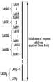
도 3을 참조하면, 호스트(Host)는 메모리 시스템(10)에 제 0 내지 제 p 논리 어드레스 넘버들(LAN0~LANp)을 전송할 수 있다. 본 발명의 실시 예에 따르면, 제 0 내지 제 p 논리 어드레스 넘버들(LAN0~LANp)은 복수의 논리 어드레스 그룹들(LAGR0~LAGRq)로 구분될 수 있다. 예를 들면, 도 3에 도시된 바와 같이 각 논리 어드레스 그룹은 4개의 논리 어드레스 넘버들을 포함할 수 있다. 각 논리 어드레스 넘버가 속하는 논리 어드레스 그룹은 해당 논리 어드레스 넘버를 4로 나눔으로써 도출되는 몫(quotient)으로 결정될 수 있다. 도 3에서, 제 0 내지 제 3 논리 어드레스 넘버들(LAN0~LAN3)은 제 0 논리 어드레스 그룹(LAGR0)을 구성한다. 제 4 내지 제 7 논리 어드레스 넘버들(LAN4~LAN7)은 제 1 논리 어드레스 그룹(LAGR1)을 구성한다. 제 8 내지 제 11 논리 어드레스 넘버들(LAN8~LAN11)은 제 2 논리 어드레스 그룹(LAGR2)을 구성한다. 제 12 내지 제 1 논리 어드레스 넘버들(LAN12~LAN15)은 제 3 논리 어드레스 그룹(LAGR3)을 구성한다. 제 p-3 내지 제 p 논리 어드레스 넘버들(LANp-3~LANp)은 제 q 논리 어드레스 넘버들(LAGRq)을 구성한다.Referring to FIG. 3, a host may transmit the 0th to the p logical address numbers (LAN0 to LANp) to the
플래시 변환 레이어(220, 도 1 참조)는 제 2 맵 테이블(MPT2)의 논리 어드레스 넘버들 각각이 속하는 논리 어드레스 그룹을 결정하고, 그에 따라 메타 정보(METI)를 생성한다.
The flash conversion layer 220 (see FIG. 1) determines the logical address group to which each logical address number of the second map table MPT2 belongs, and generates meta information (METI) accordingly.
도 4는 메모리 시스템(10)의 변형 실시 예(1000)를 보여주는 블록도이다.4 is a block diagram illustrating an
도 4를 참조하면, 메모리 시스템(1000)은 복수의 반도체 메모리 장치들(1110~11k0) 및 메모리 컨트롤러(1200)를 포함한다.Referring to FIG. 4, a
제 1 내지 제 k 반도체 메모리 장치들(1110~11k0) 각각은 도 1을 참조하여 설명된 반도체 메모리 장치(100)와 마찬가지로 구성되고, 동작할 것이다.Each of the first to k < th >
메모리 컨트롤러(1200)은 램(1210) 및 플래시 변환 레이어(1220)를 포함한다.The
메모리 컨트롤러(1200)는 제 1 내지 제 k 채널들(CH1~CHk)을 통해 제 1 내지 제 k 반도체 메모리 장치들(1110~11k0)과 통신한다.The
플래시 변환 레이어(1220)는 도 1을 참조하여 설명된 플래시 변환 레이어(220)와 마찬가지로 각 반도체 메모리 장치를 제어하도록 구성될 것이다.The
플래시 변환 레이어(1220)는 호스트(Host)로부터의 요청에 응답하여 반도체 메모리 장치들(1110~11k0)을 엑세스할 것이다. 플래시 변환 레이어(1220)는 프로그램 동작 시 요청 어드레스 넘버와 물리 어드레스 넘버 사이의 매핑 관계를 제 1 맵 테이블(MPT1) 또는 제 2 맵 테이블(MPT2)에 업데이트할 것이다. 해당 물리 어드레스 넘버가 제 1 메모리 블록 그룹(BLKG1, 도 2 참조)에 해당할 때 제 1 맵 테이블(MPT1)이 업데이트될 것이다. 해당 물리 어드레스 넘버가 제 2 메모리 블록 그룹(BLKG2, 도 2 참조)에 해당할 때 제 2 맵 테이블(MPT2)이 업데이트될 것이다. 플래시 변환 레이어(1220)는 플래시 변환 레이어(1220)는 메모리 블록들(BLK1~BLKz)의 페이지들과 해당 논리 어드레스 넘버들의 매핑 관계를 포함하는 메인 맵 테이블(MMPT)을 램(1210)에 저장하고, 제 1 및 제 2 맵 테이블들(MPT1, MPT2)에 기반하여 메인 맵 테이블(MMPT)을 업데이트할 것이다.
The
도 5는 도 4의 반도체 메모리 장치들(1110~11k0)에 포함된 메모리 블록들을 설명하기 위한 도면이다. 도 5에서, 설명의 편의를 위해 8개의 반도체 메모리 장치들(1110~118)이 제공된다고 가정한다.FIG. 5 is a view for explaining memory blocks included in the
실시 예로서, 각 반도체 메모리 장치는 싱글 레벨 셀들을 포함하거나 멀티 레벨 셀들을 포함할 수 있다. 도 5를 참조하면, 복수의 반도체 메모리 장치들(1110~1180)은 복수의 메모리 그룹들(MG1, MG2)로 구분된다. 제 1 메모리 그룹(MG1)의 메모리 셀들은 싱글 레벨 셀들로 정의될 수 있다. 제 2 메모리 그룹(MG2)의 메모리 셀들은 멀티 레벨 셀들로 정의될 수 있다.As an example, each semiconductor memory device may include single level cells or may include multi level cells. Referring to FIG. 5, a plurality of
제 1 메모리 그룹(MG1)은 제 1 내지 제 4 반도체 메모리 장치들(1110~1140)을 포함한다. 제 1 메모리 그룹(MG1)의 반도체 메모리 장치들(1110~1140) 각각은 제 1 내지 제 z 메모리 블록들(BLK11~BLK1z)을 포함하고, 제 1 내지 제 z 메모리 블록들(BLK11~BLK1z) 각각은 제 1 내지 제 n 물리 페이지들(PP11~PP1n)을 포함할 것이다. 제 1 메모리 그룹(MG1)의 메모리 셀들은 싱글 레벨 셀들이므로, 제 1 내지 제 n 물리 페이지들(PP11~PP1n)은 하나의 논리 페이지(LP)를 포함할 것이다.The first memory group MG1 includes the first to fourth
제 2 메모리 그룹(MG2)은 제 5 내지 제 8 반도체 메모리 장치들(1150~1180)을 포함한다. 제 2 메모리 그룹(MG2)의 반도체 메모리 장치들(1150~1180) 각각은 제 1 내지 제 z 메모리 블록들(BLK21~BLK2z)을 포함하고, 제 1 내지 제 z 메모리 블록들(BLK21~BLK2z) 각각은 제 1 내지 제 n 물리 페이지들(PP21~PP2n)을 포함할 것이다. 제 2 메모리 그룹(MG2)의 메모리 셀들은 멀티 레벨 셀들이므로, 제 1 내지 제 n 물리 페이지들(PP21~PP2n) 각각은 복수의 논리 페이지들(LPs), 예를 들면 2개의 논리 페이지들(LPs)을 포함할 것이다.The second memory group MG2 includes the fifth to eighth
본 발명의 기술적 사상은 도 4의 실시 예에도 적용된다. 메모리 시스템(1000, 도 4 참조) 내 각 반도체 메모리 장치가 싱글 레벨 셀들 또는 멀티 레벨 셀들을 포함하는 것은, 메모리 시스템(1000) 내 각 메모리 블록이 싱글 레벨 셀들 또는 멀티 레벨 셀들을 포함하는 것을 의미할 것이다. 예를 들면, 도 5의 메모리 블록(BLK12)은 싱글 레벨 셀들을 포함하고, 따라서 메모리 블록(BLK12)의 각 물리 페이지는 하나의 논리 페이지(LP)를 포함할 것이다. 예를 들면, 메모리 블록(BLK22)은 멀티 레벨 셀들을 포함하고, 따라서 메모리 블록(BLK22)의 각 물리 페이지는 복수의 논리 페이지들(LPs)을 포함할 것이다.The technical idea of the present invention is also applied to the embodiment of Fig. The fact that each semiconductor memory device in memory system 1000 (see FIG. 4) includes single level cells or multi level cells means that each memory block in
이하, 설명의 편의를 위해 도 1의 실시 예를 기준으로 본 발명의 실시 예가 설명된다.
Hereinafter, for convenience of description, an embodiment of the present invention will be described based on the embodiment of FIG.
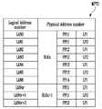
도 6은 도 1의 제 1 맵 테이블(MPT1)을 보여주는 도면이다.FIG. 6 is a diagram showing the first map table MPT1 of FIG. 1. FIG.
도 6을 참조하면, 논리 어드레스 넘버와 해당 물리 어드레스 넘버가 제 1 맵 테이블(MPT1)에 저장되어 있다. 호스트(Host)로부터 프로그램 동작을 위한 요청 어드레스 넘버가 수신될 때, 플래시 변환 레이어(220)는 특정 물리 어드레스 넘버를 매핑할 것이다. 플래시 변환 레이어(220)는 랜덤한 요청 어드레스 넘버들이 수신될 때 제 1 메모리 블록 그룹(BLKG1, 도 2 참조)에 해당하는 물리 어드레스 넘버를 매핑한다. 예를 들면, 호스트(Host, 도 1 참조)는 1개 섹터에 해당하는 요청 어드레스 넘버에 대한 프로그램 요청을 반복적으로 전송할 수 있다. 전송된 요청 어드레스 넘버들(예를 들면 LAN100, LAN200, LAN50, LAN77, LAN140) 각각은 제 1 메모리 블록 그룹(BLKG1) 내 페이지에 매핑될 것이다.Referring to FIG. 6, the logical address number and the corresponding physical address number are stored in the first map table MPT1. When a request address number for a program operation is received from the host, the
도 6에서, 제 100 논리 어드레스 넘버(LAN100)는 제 2 메모리 블록(BLK2)의 제 1 물리 페이지(PP21)에 매핑된다. 제 200 논리 어드레스 넘버(LAN200)는 제 2 메모리 블록(BLK2)의 제 2 물리 페이지(PP22)에 매핑된다. 제 50 논리 어드레스 넘버(LAN50)는 제 2 메모리 블록(BLK2)의 제 3 물리 페이지(PP23)에 매핑된다. 제 77 논리 어드레스 넘버(LAN77)는 제 2 메모리 블록(BLK2)의 제 4 물리 페이지(PP24)에 매핑된다. 제 140 논리 어드레스 넘버(LAN140)는 제 2 메모리 블록(BLK2)의 제 5 물리 페이지(PP25)에 매핑된다.
In Fig. 6, the 100th logical address number (LAN100) is mapped to the first physical page PP21 of the second memory block BLK2. The 200th logical address number (LAN 200) is mapped to the second physical page PP22 of the second memory block BLK2. The 50th logical address number (LAN50) is mapped to the third physical page PP23 of the second memory block BLK2. The 77th logical address number (LAN77) is mapped to the fourth physical page (PP24) of the second memory block (BLK2). The 140th logical address number (LAN 140) is mapped to the fifth physical page PP25 of the second memory block BLK2.
도 7은 도 1의 제 2 맵 테이블(MPT2)을 보여주는 도면이다.FIG. 7 is a diagram showing a second map table MPT2 of FIG. 1. FIG.
도 7을 참조하면, 제 2 맵 테이블(MPT2)은 논리 어드레스 넘버와 해당 물리 어드레스 넘버를 포함한다. 플래시 변환 레이어(220)는 프로그램 동작을 위한 순차적인 요청 어드레스 넘버들이 수신될 때 요청 어드레스들 각각을 제 2 메모리 블록 그룹(BLKG2, 도 2 참조)에 해당하는 물리 어드레스 넘버에 매핑한다. 예를 들면, 호스트(Host)는 시작 섹터(예를 들면, LAN0)와 섹터들의 개수 정보(예를 들면 6)를 전송함으로써 요청 어드레스 넘버들을 특정할 수 있다. 전송된 요청 어드레스 넘버들(예를 들면, LAN0~LAN6) 각각은 제 2 메모리 블록 그룹(BLKG2) 내 페이지에 매핑될 것이다.Referring to FIG. 7, the second map table MPT2 includes a logical address number and a corresponding physical address number. The
도 6에서, 제 0 및 제 1 논리 어드레스 넘버들(LAN0, LAN1)은 제 x 메모리 블록(BLKx) 내 제 1 물리 페이지(PP11)의 논리 페이지들(LP1, LP2)에 매핑된다. 제 2 및 제 3 논리 어드레스 넘버들(LAN2, LAN3)은 제 x 메모리 블록(BLKx) 내 제 2 물리 페이지(PP12)의 논리 페이지들(LP1, LP2)에 매핑된다. 제 4 및 제 5 논리 어드레스 넘버들(LAN4, LAN5)은 제 x 메모리 블록(BLKx) 내 제 3 물리 페이지(PP13)의 논리 페이지들(LP1, LP2)에 매핑된다. 제 6 논리 어드레스 넘버(LAN6)는 제 x 메모리 블록(BLKx) 내 제 4 물리 페이지(PP14)의 논리 페이지(LP1)에 매핑된다. 제 4r 및 제 4r+1 논리 어드레스 넘버들(LAN4r, LAN4r+1)은 제 x+1 메모리 블록(BLKx+1) 내 제 1 물리 페이지(PP11)의 논리 페이지들(LP1, LP2)에 매핑된다. 제 4r+2 논리 어드레스 넘버(LAN4r+2)은 제 x+1 메모리 블록(BLKx+1) 내 제 2 물리 페이지(PP12)의 논리 페이지(LP1)에 매핑된다.6, the 0th and 1st logical address numbers LAN0 and LAN1 are mapped to the logical pages LP1 and LP2 of the first physical page PP11 in the xth memory block BLKx. The second and third logical address numbers LAN2 and LAN3 are mapped to the logical pages LP1 and LP2 of the second physical page PP12 in the xth memory block BLKx. The fourth and fifth logical address numbers LAN4 and LAN5 are mapped to the logical pages LP1 and LP2 of the third physical page PP13 in the xth memory block BLKx. The sixth logical address number LAN6 is mapped to the logical page LP1 of the fourth physical page PP14 in the xth memory block BLKx. The 4r and 4r + 1 logical address numbers LAN4r and LAN4r + 1 are mapped to the logical pages LP1 and LP2 of the first physical page PP11 in the (x + 1) th memory
결과적으로 제 x 및 제 x+1 메모리 블록들(BLKx, BLKx+1)은 순차적인 논리 어드레스 넘버들에 해당하는 데이터를 저장한다.
As a result, the x and x + 1 memory blocks (BLKx, BLKx + 1) store data corresponding to sequential logical address numbers.
도 8은 도 1의 메인 맵 테이블(MMPT)을 보여주는 도면이다.8 is a view showing the main map table MMPT of FIG.
도 8을 참조하면, 메인 맵 테이블(MMPT)은 호스트(Host)로부터 수신될 수 있는 논리 어드레스 넘버들(LAN0~LANp), 그리고 해당 물리 어드레스 넘버들(PAN0~PANp)을 저장할 것이다. 각 물리 어드레스 넘버는, 특정 물리 페이지 및 논리 페이지에 대한 정보를 포함할 것이다.Referring to FIG. 8, the main map table MMPT will store logical address numbers (LAN0 to LANp) and corresponding physical address numbers (PAN0 to PANp) that can be received from a host. Each physical address number will contain information about a particular physical page and a logical page.
실시 예로서, 램(210) 내 메인 맵 테이블(MMPT)을 저장하기 위한 저장 공간에 따라, 메인 맵 테이블(MMPT) 중 일부만 램(210)에 저장될 수 있다. 예를 들면, 메인 맵 테이블(MMPT)은 반도체 메모리 장치(100) 내 메타 블록에 저장되고, 메인 맵 테이블(MMPT) 중 일부만 램(210)에 로드될 수 있다.
As an embodiment, only a part of the main map table MMPT may be stored in the
도 9는 본 발명의 실시 예에 따른 메타 정보(METI)를 설명하기 위한 도면이다.9 is a diagram for explaining meta information (METI) according to an embodiment of the present invention.
도 9를 참조하면, 제 2 맵 테이블(MPT2)에 포함된 논리 어드레스 넘버들(LAN0~LAN6, LAN4r~LAN4r+2)에 따라 메타 정보(METI)가 생성된다. 플래시 변환 레이어(220)는 제 2 맵 테이블(MPT2)에 포함된 논리 어드레스 넘버들이 속하는 논리 어드레스 그룹들을 메타 정보(METI)로서 정의할 것이다.Referring to FIG. 9, meta information (METI) is generated in accordance with logical address numbers (LAN0 to LAN6, LAN4r to LAN4r + 2) included in the second map table MPT2. The
예를 들면, 논리 어드레스 그룹은 각 논리 어드레스 넘버를 4로 나눔으로써 도출되는 몫(quotient)으로 결정될 수 있다. 도 9에 도시된 바와 같이, 제 0 내지 제 3 논리 어드레스 넘버들(LAN0~LAN3)은 제 0 논리 어드레스 그룹(LAGR0)으로 결정된다. 제 4 내지 제 6 논리 어드레스 넘버들(LAN4~LAN6)은 제 1 논리 어드레스 그룹(LAGR1)으로 결정된다. 제 4r 내지 제 4r+2 논리 어드레스 넘버들(LAN4r~LAN4r+2)은 제 r 논리 어드레스 그룹(LAGRr)으로 결정된다.For example, the logical address group can be determined as a quotient derived by dividing each logical address number by four. As shown in Fig. 9, the 0th to 3rd logical address numbers (LAN0 to LAN3) are determined as the 0th logical address group LAGR0. The fourth to sixth logical address numbers (LAN4 to LAN6) are determined as the first logical address group LAGR1. The 4 r to 4 r + 2 logical address numbers (LAN4r to LAN4r + 2) are determined as the r logical address group LAGRr.
제 2 맵 테이블(MPT2)에는 순차적인 논리 어드레스 넘버들(LAN0~LAN6, LAN4r~LAN4+2)이 포함되어 있다. 따라서 제 2 맵 테이블(MPT2)에 포함된 논리 어드레스 넘버들(LAN0~LAN6, LAN4r~LAN4+2)의 수보다 메타 정보(METI)에 포함된 논리 어드레스 그룹들(LAGR0, LAGR1, LAGRr)의 수는 현저히 감소할 것이다.
The second map table MPT2 includes sequential logical address numbers (LAN0 to LAN6, LAN4r to LAN4 + 2). Therefore, the number of logical address groups LAGR0, LAGR1, LAGRr included in the meta information METI than the number of logical address numbers (LAN0 to LAN6, LAN4r to LAN4 + 2) included in the second map table MPT2 Will decrease significantly.
도 10은 본 발명의 실시 예에 따른 컨트롤러(200)의 동작 방법을 보여주는 순서도이다.10 is a flowchart showing an operation method of the
도 1, 도 7 및 도 10을 참조하면, S110단계에서, 컨트롤러(200)는 메타 정보(METI)를 생성한다. 컨트롤러(200)는 제 2 맵 테이블(MPT2)의 논리 어드레스 넘버들이 속하는 논리 어드레스 그룹들을 판별하고, 판별된 논리 어드레스 그룹들을 메타 정보(METI)로서 생성한다.Referring to FIGS. 1, 7 and 10, in step S110, the
S120단계에서, 호스트(Host)로부터 읽기 요청을 위한 요청 어드레스 넘버가 수신된다. 이에 따라 요청 어드레스 넘버에 해당하는 물리 어드레스 넘버의 검출이 요구된다.In step S120, a request address number for a read request is received from the host. Accordingly, detection of the physical address number corresponding to the requested address number is required.
S130단계에서, 먼저 컨트롤러(200)는 요청 어드레스 넘버가 속하는 논리 어드레스 그룹을 판별한다. 예를 들면, 컨트롤러(200)는 요청 어드레스 넘버를 4로 나눔으로써 도출되는 몫을 계산할 것이다.In step S130, the
S140단계에서, 컨트롤러(200)는 판별된 논리 어드레스 그룹이 메타 정보(METI)에 포함된 논리 어드레스 그룹들(LAGR0, LAGR1, LAGRr, 도 9 참조) 내에 존재하는지 여부를 감지한다. 만약 존재한다면, S150단계가 수행된다. 만약 그렇지 않다면 S160단계가 수행된다.In step S140, the
S150단계에서, 컨트롤러(200)는 제 2 맵 테이블(MPT2)에서 요청 어드레스 넘버를 서치한다. 즉 판별된 논리 어드레스 그룹이 메타 정보(METI)에 포함된 논리 어드레스 그룹들(LAGR0, LAGR1, LAGRr) 내에 존재하는지에 따라, 컨트롤러(200)는 제 2 맵 테이블(MPT2)을 선택적으로 서치한다.In step S150, the
제 2 맵 테이블(MPT2) 내에 요청 어드레스 넘버가 존재하지 않을 때 S160단계가 수행된다. 제 2 맵 테이블(MPT2) 내에 요청 어드레스 넘버가 존재할 때 S180단계가 수행된다.When the request address number does not exist in the second map table MPT2, step S160 is performed. When the request address number is present in the second map table MPT2, step S180 is performed.
예를 들면, 요청 어드레스 넘버가 제 6 논리 어드레스 넘버(LAN6)라고 가정한다. 요청 어드레스 넘버는 제 1 논리 어드레스 그룹(LAGR1)에 속하고, 제 1 논리 어드레스 그룹(LAGR1)은 메타 정보(METI)의 논리 어드레스 그룹들(LAGR0, LAGR1, LAGRr)에 포함된다. 따라서 제 2 맵 테이블(MPT2) 내에서 요청 어드레스 넘버가 서치될 것이다. 도 6과 같이 제 2 맵 테이블(MPT2) 내에 제 6 논리 어드레스 넘버(LAN6)가 포함되는 경우, S150단계에서의 서치는 성공할 것이다. 이러한 경우 제 x 메모리 블록(BLKx)의 제 4 물리 페이지(PP14)의 논리 어드레스(LP1)가 물리 어드레스 넘버로서 검출될 것이다.For example, it is assumed that the request address number is the sixth logical address number (LAN6). The requested address number belongs to the first logical address group LAGR1 and the first logical address group LAGR1 is included in the logical address groups LAGR0, LAGR1 and LAGRr of the meta information METI. Therefore, the request address number will be searched in the second map table MPT2. When the sixth logical address number (LAN6) is included in the second map table MPT2 as shown in Fig. 6, the search in step S150 will succeed. In this case, the logical address LP1 of the fourth physical page PP14 of the xth memory block BLKx will be detected as the physical address number.
예를 들면, 요청 어드레스 넘버가 제 7 논리 어드레스 넘버(LAN7)라고 가정한다. 요청 어드레스 넘버는 제 1 논리 어드레스 그룹(LAGR1)에 속하고, 제 1 논리 어드레스 그룹(LAGR1)은 메타 정보(METI)의 논리 어드레스 그룹들(LAGR0, LAGR1, LAGRr)에 포함된다. 이때 제 2 맵 테이블(MPT2) 내에서 요청 어드레스 넘버가 서치될 것이다. 그러나 도 6과 같이 제 2 맵 테이블(MPT2) 내에 제 7 논리 어드레스 넘버(LAN7)가 존재하지 않는 경우 S150단계에서의 서치는 실패할 것이다.For example, it is assumed that the request address number is the seventh logical address number (LAN7). The requested address number belongs to the first logical address group LAGR1 and the first logical address group LAGR1 is included in the logical address groups LAGR0, LAGR1 and LAGRr of the meta information METI. At this time, the request address number will be searched in the second map table MPT2. However, if the seventh logical address number LAN7 does not exist in the second map table MPT2 as shown in Fig. 6, the search in step S150 will fail.
S160단계 및 S170단계에서, 제 1 맵 테이블(MPT1) 및 메인 맵 테이블(MMPT)이 차례로 서치된다. S160단계에서, 컨트롤러(200)는 제 1 맵 테이블(MPT1) 내에서 요청 어드레스 넘버를 서치한다. 제 1 맵 테이블(MPT1) 내에서 요청 어드레스 넘버가 존재하지 않을 때, S170단계가 수행된다. 제 1 맵 테이블(MPT1) 내에서 요청 어드레스 넘버가 존재할 때 S180단계가 수행된다.In steps S160 and S170, the first map table MPT1 and the main map table MMPT are sequentially searched. In step S160, the
S170단계에서, 컨트롤러(200)는 메인 맵 테이블(MMPT) 내에서 요청 어드레스 넘버를 서치한다.In step S170, the
S180단계에서, 컨트롤러(200)는 서치를 성공한 맵 테이블로부터 물리 어드레스 넘버를 검출한다. 검출된 물리 어드레스 넘버를 반도체 메모리 장치(100)로 제공할 것이다.In step S180, the
본 발명의 실시 예에 따르면, 요청 어드레스 넘버가 속하는 논리 어드레스 그룹이 메타 정보(METI)의 논리 어드레스 그룹들 내에 존재하는지 여부를 감지하고, 감지 결과에 따라 제 1 맵 테이블(MPT1)을 선택적으로 서치한다. 제 1 맵 테이블(MPT1)에 대한 서치를 생략하는 것은, 물리 어드레스 넘버를 검출하는 것에 소요되는 시간이 감소됨을 의미한다. 제 1 맵 테이블(MPT1)의 용량이 커질수록, 제 1 맵 테이블(MPT1)에 대한 서치를 생략하는 것에 의해 상기 소요 시간은 크게 감소할 수 있다. 따라서, 향상된 동작 속도를 갖는 메모리 시스템(10)이 제공된다.
According to an embodiment of the present invention, it is possible to detect whether a logical address group to which a request address number belongs exists in logical address groups of meta information (METI), and selectively search the first map table (MPT1) do. Omitting the search for the first map table MPT1 means that the time required for detecting the physical address number is reduced. As the capacity of the first map table MPT1 becomes larger, the required time can be greatly reduced by omitting the search for the first map table MPT1. Thus, a
도 11은 도 1의 메모리 시스템(10)의 구현 례(2000)를 보여주는 블록도이다.FIG. 11 is a block diagram illustrating an
도 11을 참조하면, 메모리 시스템(2000)은 반도체 메모리 장치(100) 및 컨트롤러(1200)를 포함한다.11, the
반도체 메모리 장치(100)는 도 1을 참조하여 설명된 바와 마찬가지로 구성되고, 동작할 수 있다. 이하, 중복되는 설명은 생략된다.The
컨트롤러(2200)는 호스트(Host) 및 반도체 메모리 장치(100)에 연결된다. 컨트롤러(2200)는 램(2210, Random Access Memory), 프로세싱 유닛(2220, processing unit), 호스트 인터페이스(2230, host interface), 메모리 인터페이스(2240, memory interface) 및 에러 정정 블록(2250)을 포함한다.The
램(2210)은 프로세싱 유닛(2220)의 동작 메모리, 반도체 메모리 장치(100) 및 호스트(Host) 사이의 캐시 메모리, 그리고 반도체 메모리 장치(100) 및 호스트(Host) 사이의 버퍼 메모리 중 적어도 하나로서 이용된다. 프로세싱 유닛(2220)은 컨트롤러(2200)의 제반 동작을 제어한다. 프로세싱 유닛(2220) 및 램(2210)은 도 1을 참조하여 설명된 플래시 변환 레이어(220)의 기능을 수행할 수 있다. 예를 들면, 플래시 변환 레이어(220)의 기능을 수행하기 위한 프로그램 코드가 반도체 메모리 장치(100)에 저장되고, 그러한 프로그램 코드가 램(2210)에 로드되고, 프로세싱 유닛(2220)은 램(2210)에 로드된 프로그램 코드를 실행하여 플래시 변환 레이어(220)의 기능을 수행할 수 있다. 예를 들면, 프로세싱 유닛(2220)은 펌웨어(firmware)를 구동함으로써 플래시 변환 레이어(220)의 기능을 수행할 수 있다.The
호스트 인터페이스(2230)는 호스트(Host) 및 컨트롤러(2200) 사이의 데이터 교환을 수행하기 위한 프로토콜을 포함한다. 예시적인 실시 예로서, 컨트롤러(2200)는 USB (Universal Serial Bus) 프로토콜, MMC (multimedia card) 프로토콜, PCI (peripheral component interconnection) 프로토콜, PCI-E (PCI-express) 프로토콜, ATA (Advanced Technology Attachment) 프로토콜, Serial-ATA 프로토콜, Parallel-ATA 프로토콜, SCSI (small computer small interface) 프로토콜, ESDI (enhanced small disk interface) 프로토콜, 그리고 IDE (Integrated Drive Electronics) 프로토콜, 사유(private) 프로토콜 등과 같은 다양한 인터페이스 프로토콜들 중 적어도 하나를 통해 호스트(Host)와 통신하도록 구성된다.The
메모리 인터페이스(2240)는 반도체 메모리 장치(100)와 인터페이싱한다. 예를 들면, 메모리 인터페이스는 낸드 인터페이스 또는 노어 인터페이스를 포함한다.The
에러 정정 블록(2250)은 에러 정정 코드(ECC, Error Correcting Code)를 이용하여 반도체 메모리 장치(100)로부터 수신된 데이터의 에러를 검출하고, 정정하도록 구성된다.The
컨트롤러(2200) 및 반도체 메모리 장치(100)는 하나의 반도체 장치로 집적될 수 있다. 예시적인 실시 예로서, 컨트롤러(2200) 및 반도체 메모리 장치(100)는 하나의 반도체 장치로 집적되어, 메모리 카드를 구성할 수 있다. 예를 들면, 컨트롤러(2200) 및 반도체 메모리 장치(100)는 하나의 반도체 장치로 집적되어 PC 카드(PCMCIA, personal computer memory card international association), 컴팩트 플래시 카드(CF), 스마트 미디어 카드(SM, SMC), 메모리 스틱, 멀티미디어 카드(MMC, RS-MMC, MMCmicro), SD 카드(SD, miniSD, microSD, SDHC), 유니버설 플래시 기억장치(UFS) 등과 같은 메모리 카드를 구성할 것이다.The
컨트롤러(2200) 및 반도체 메모리 장치(100)는 하나의 반도체 장치로 집적되어 반도체 드라이브(SSD, Solid State Drive)를 구성할 수 있다. 반도체 드라이브(SSD)는 반도체 메모리에 데이터를 저장하도록 구성되는 저장 장치를 포함한다. 메모리 시스템(2000)이 반도체 드라이브(SSD)로 이용되는 경우, 메모리 시스템(2000)에 연결된 호스트(Host)의 동작 속도는 획기적으로 개선된다.The
다른 예로서, 메모리 시스템(2000)은 컴퓨터, UMPC (Ultra Mobile PC), 워크스테이션, 넷북(net-book), PDA (Personal Digital Assistants), 포터블(portable) 컴퓨터, 웹 타블렛(web tablet), 무선 전화기(wireless phone), 모바일 폰(mobile phone), 스마트폰(smart phone), e-북(e-book), PMP(portable multimedia player), 휴대용 게임기, 네비게이션(navigation) 장치, 블랙박스(black box), 디지털 카메라(digital camera), 3차원 수상기(3-dimensional television), 디지털 음성 녹음기(digital audio recorder), 디지털 음성 재생기(digital audio player), 디지털 영상 녹화기(digital picture recorder), 디지털 영상 재생기(digital picture player), 디지털 동영상 녹화기(digital video recorder), 디지털 동영상 재생기(digital video player), 정보를 무선 환경에서 송수신할 수 있는 장치, 홈 네트워크를 구성하는 다양한 전자 장치들 중 하나, 컴퓨터 네트워크를 구성하는 다양한 전자 장치들 중 하나, 텔레매틱스 네트워크를 구성하는 다양한 전자 장치들 중 하나, RFID 장치, 또는 컴퓨팅 시스템을 구성하는 다양한 구성 요소들 중 하나 등과 같은 전자 장치의 다양한 구성 요소들 중 하나로 제공된다.As another example, the
예시적인 실시 예로서, 반도체 메모리 장치(100) 또는 메모리 시스템(2000)은 다양한 형태들의 패키지로 실장될 수 있다. 예를 들면, 반도체 메모리 장치(100) 또는 메모리 시스템(2000)은 PoP(Package on Package), Ball grid arrays(BGAs), Chip scale packages(CSPs), Plastic Leaded Chip Carrier(PLCC), Plastic Dual In Line Package(PDIP), Die in Waffle Pack, Die in Wafer Form, Chip On Board(COB), Ceramic Dual In Line Package(CERDIP), Plastic Metric Quad Flat Pack(MQFP), Thin Quad Flatpack(TQFP), Small Outline integrated circuit (SOIC), Shrink Small Outline Package(SSOP), Thin Small Outline Package(TSOP), Thin Quad Flatpack(TQFP), System In Package(SIP), Multi Chip Package(MCP), Wafer-level Fabricated Package(WFP), Wafer-Level Processed Stack Package(WSP) 등과 같은 방식으로 패키지화되어 실장될 수 있다.As an exemplary embodiment,
본 발명의 실시 예에 따르면, 요청 어드레스 넘버가 속하는 논리 어드레스 그룹이 메타 정보의 논리 어드레스 그룹들 내에 존재하는지 여부를 감지하고, 감지 결과에 따라 제 1 맵 테이블을 선택적으로 서치한다. 따라서, 향상된 동작 속도를 갖는 메모리 시스템이 제공된다.
According to an embodiment of the present invention, it is detected whether a logical address group to which a request address number belongs exists in logical address groups of meta information, and selectively searches the first map table according to the detection result. Thus, a memory system with improved operating speed is provided.
본 발명의 상세한 설명에서는 구체적인 실시 예에 관하여 설명하였으나, 본 발명의 범위와 기술적 사상에서 벗어나지 않는 한도 내에서 다양한 변경이 가능하다. 그러므로 본 발명의 범위는 상술한 실시 예에 국한되어 정해져서는 안되며 후술하는 특허청구범위뿐만 아니라 이 발명의 특허청구범위와 균등한 것들에 의해 정해져야 한다.While the invention has been shown and described with reference to certain preferred embodiments thereof, it will be understood by those skilled in the art that various changes and modifications may be made without departing from the spirit and scope of the invention. Therefore, the scope of the present invention should not be limited to the above-described embodiments, but should be determined by the equivalents of the claims of the present invention as well as the claims of the following.
100: 반도체 메모리 장치
110: 메모리 셀 어레이
120: 주변 회로
200: 컨트롤러
210: 램
220: 플래시 변환 레이어
MPT1: 제 1 맵 테이블
MPT2: 제 2 맵 테이블
MMPT: 메인 맵 테이블
BLKG1: 제 1 메모리 블록 그룹
BLKG2: 제 2 메모리 블록 그룹100: semiconductor memory device
110: memory cell array
120: peripheral circuit
200: controller
210: RAM
220: Flash conversion layer
MPT1: First map table
MPT2: second map table
MMPT: Main map table
BLKG1: first memory block group
BLKG2: second memory block group
Claims (15)
Translated fromKorean상기 호스트로부터 수신되는 복수의 논리 어드레스 넘버들은 복수의 논리 어드레스 그룹들로 구분되되,
상기 멀티 레벨 셀들을 갖는 상기 메모리 블록들의 페이지들 중 적어도 일부를 가리키는 제 1 물리 어드레스 넘버들 및 상기 복수의 논리 어드레스 넘버들 중 제 1 논리 어드레스 넘버들 사이의 매핑 관계를 포함하는 제 1 맵 테이블을 저장하는 단계;
상기 제 1 논리 어드레스 넘버들이 속하는 논리 어드레스 그룹들을 메타 정보로서 저장하는 단계;
호스트로부터 상기 복수의 논리 어드레스 넘버들 중 어느 하나를 요청 어드레스 넘버로서 수신하는 단계;
상기 복수의 논리 어드레스 그룹들 중 상기 요청 어드레스 넘버가 속하는 논리 어드레스 그룹을 판별하는 단계; 및
상기 판별된 논리 어드레스 그룹이 상기 메타 정보의 논리 어드레스 그룹들 내에 존재하는지 여부를 감지하고, 상기 감지 결과에 따라 상기 제 1 맵 테이블 내에서 상기 요청 어드레스 넘버를 서치하는 단계를 포함하는 동작 방법.CLAIMS What is claimed is: 1. A method of operating a memory system comprising a controller coupled to a host and a semiconductor memory device coupled to the controller, the semiconductor memory device comprising memory blocks having multi-level cells,
Wherein the plurality of logical address numbers received from the host are divided into a plurality of logical address groups,
A first map table containing first physical address numbers indicating at least some of the pages of the memory blocks having the multi-level cells and a mapping relationship between first logical address numbers of the plurality of logical address numbers, Storing;
Storing logical address groups to which the first logical address numbers belong as meta information;
Receiving from the host any of the plurality of logical address numbers as a request address number;
Determining a logical address group to which the request address number belongs among the plurality of logical address groups; And
Detecting whether the determined logical address group is present in logical address groups of the meta information and searching the request address number in the first map table according to the detection result.
상기 서치하는 단계는,
상기 판별된 논리 어드레스 그룹이 상기 메타 정보의 논리 어드레스 그룹들 내에 존재할 때 상기 제 1 맵 테이블 내에서 상기 요청 어드레스 넘버를 서치하는 단계를 포함하는 동작 방법.The method according to claim 1,
Wherein the searching comprises:
And searching the request address number in the first map table when the determined logical address group is within logical address groups of the meta information.
상기 반도체 메모리 장치는 싱글 레벨 셀들을 갖는 메모리 블록들을 더 포함하는 동작 방법.The method according to claim 1,
Wherein the semiconductor memory device further comprises memory blocks having single level cells.
상기 싱글 레벨 셀들을 포함하는 상기 메모리 블록들의 페이지들 중 적어도 일부를 가리키는 제 2 물리 어드레스 넘버들 및 상기 복수의 논리 어드레스 넘버들 중 제 2 논리 어드레스 넘버들 사이의 매핑 관계를 포함하는 제 2 맵 테이블을 저장하는 단계를 더 포함하는 동작 방법.The method of claim 3,
A second map table including second physical address numbers indicating at least some of the pages of the memory blocks including the single level cells and a mapping relationship between second logical address numbers of the plurality of logical address numbers, ≪ / RTI >
상기 판별된 논리 어드레스 그룹이 상기 메타 정보의 논리 어드레스 그룹들 내에 존재하지 않을 때 상기 제 2 맵 테이블 내에서 상기 요청 어드레스 넘버를 서치하는 단계를 더 포함하는 동작 방법.5. The method of claim 4,
And searching the request address number in the second map table when the determined logical address group is not in logical address groups of the meta information.
상기 복수의 논리 어드레스 넘버들과 제 3 물리 어드레스 넘버들 사이의 매핑 관계를 포함하는 제 3 맵 테이블을 저장하는 단계를 더 포함하되,
제 3 물리 어드레스 넘버들은 상기 멀티 레벨 셀들을 갖는 상기 메모리 블록들의 페이지들 및 상기 싱글 레벨 셀들을 갖는 상기 메모리 블록들의 페이지들에 대응하는 동작 방법.6. The method of claim 5,
Further comprising storing a third map table that includes a mapping relationship between the plurality of logical address numbers and third physical address numbers,
Wherein the third physical address numbers correspond to pages of the memory blocks having the multi-level cells and pages of the memory blocks having the single level cells.
상기 제 2 맵 테이블 내에 상기 요청 어드레스 넘버가 존재할 때 상기 제 2 맵 테이블로부터 상기 요청 어드레스 넘버에 대응하는 물리 어드레스를 검출하는 단계; 및
상기 제 2 맵 테이블 내에 상기 요청 어드레스 넘버가 존재하지 않을 때 상기 제 3 맵 테이블 내에서 상기 요청 어드레스 넘버를 서치하는 단계를 더 포함하는 동작 방법.The method according to claim 6,
Detecting a physical address corresponding to the requested address number from the second map table when the requested address number is present in the second map table; And
And searching the request address number in the third map table when the request address number is not present in the second map table.
상기 제 3 맵 테이블로부터 상기 요청 어드레스 넘버에 대응하는 물리 어드레스를 검출하는 단계를 더 포함하는 동작 방법.8. The method of claim 7,
And detecting a physical address corresponding to the request address number from the third map table.
상기 반도체 메모리 장치와 호스트 사이에 연결되는 컨트롤러를 포함하고,
상기 호스트로부터 상기 컨트롤러로 수신되는 복수의 논리 어드레스 넘버들은 복수의 논리 어드레스 그룹들로 구분되며,
상기 컨트롤러는 상기 제 1 메모리 블록들의 페이지들 중 적어도 일부를 가리키는 제 1 물리 어드레스 넘버들 및 상기 복수의 논리 어드레스 넘버들 중 제 1 논리 어드레스 넘버들 사이의 매핑 관계를 포함하는 제 1 맵 테이블을 저장하는 램; 및
상기 제 1 논리 어드레스 넘버들이 속하는 논리 어드레스 그룹들을 메타 정보로서 상기 램에 저장하도록 구성되는 플래시 변환 레이어를 포함하되,
상기 플래시 변환 레이어는 상기 호스트로부터 상기 복수의 논리 어드레스 넘버들 중 어느 하나를 요청 어드레스 넘버로서 수신하고, 상기 요청 어드레스 넘버가 속하는 논리 어드레스 그룹을 판별하고, 상기 판별된 논리 어드레스 그룹이 상기 메타 정보의 논리 어드레스 그룹들 내에 존재할 때 상기 제 1 맵 테이블 내에서 상기 요청 어드레스 넘버를 서치하는 메모리 시스템.A semiconductor memory device including first memory blocks having multi-level cells and second memory blocks having single level cells; And
And a controller connected between the semiconductor memory device and the host,
A plurality of logical address numbers received from the host to the controller are divided into a plurality of logical address groups,
The controller stores a first map table containing first physical address numbers indicating at least some of the pages of the first memory blocks and a mapping relationship between first logical address numbers of the plurality of logical address numbers Ram; And
And a flash translation layer configured to store in the RAM the logical address groups to which the first logical address numbers belong, as meta information,
Wherein the flash conversion layer receives any one of the plurality of logical address numbers from the host as a request address number, determines a logical address group to which the requested address number belongs, And searches the request address number within the first map table when present in logical address groups.
상기 램은 상기 제 2 메모리 블록들의 페이지들 중 적어도 일부를 가리키는 제 2 물리 어드레스 넘버들 및 상기 복수의 논리 어드레스 넘버들 중 제 2 논리 어드레스 넘버들 사이의 매핑 관계를 포함하는 제 2 맵 테이블을 저장하는 메모리 시스템.10. The method of claim 9,
The ram stores a second map table containing second physical address numbers indicating at least some of the pages of the second memory blocks and a mapping relationship between second logical address numbers of the plurality of logical address numbers Memory system.
상기 플래시 변환 레이어는 상기 판별된 논리 어드레스 그룹이 상기 메타 정보의 논리 어드레스 그룹들 내에 존재하지 않을 때 상기 제 2 맵 테이블 내에서 상기 요청 어드레스 넘버를 서치하는 메모리 시스템.11. The method of claim 10,
Wherein the flash translation layer searches the request address number in the second map table when the determined logical address group is not in logical address groups of the meta information.
상기 플래시 변환 레이어는 상기 제 1 맵 테이블 내에 상기 요청 어드레스 넘버가 존재할 때 상기 제 1 맵 테이블로부터 해당 물리 어드레스를 검출하고, 상기 제 1 맵 테이블 내에 상기 요청 어드레스 넘버가 존재하지 않을 때 상기 제 2 맵 테이블 내에서 상기 요청 어드레스 넘버를 서치하는 메모리 시스템.10. The method of claim 9,
Wherein the flash translation layer detects a corresponding physical address from the first map table when the requested address number is present in the first map table, and when the requested address number is not present in the first map table, And to search the request address number within the table.
상기 램은 상기 복수의 논리 어드레스 넘버들과 제 3 물리 어드레스 넘버들 사이의 매핑 관계를 포함하는 제 3 맵 테이블을 저장하되,
제 3 물리 어드레스 넘버들은 상기 제 1 메모리 블록들의 페이지들 및 상기 제 2 메모리 블록들의 페이지들에 대응하는 메모리 시스템.10. The method of claim 9,
Wherein the RAM stores a third map table including a mapping relationship between the plurality of logical address numbers and third physical address numbers,
Wherein the third physical address numbers correspond to pages of the first memory blocks and pages of the second memory blocks.
상기 플래시 변환 레이어는 상기 판별된 논리 어드레스 그룹이 상기 메타 정보의 논리 어드레스 그룹들 내에 존재하지 않을 때 상기 제 3 맵 테이블 내에서 상기 요청 어드레스 넘버를 서치하는 메모리 시스템.14. The method of claim 13,
Wherein the flash translation layer searches the request address number in the third map table when the determined logical address group is not present in logical address groups of the meta information.
상기 플래시 변환 레이어는 상기 제 1 맵 테이블 내에 상기 요청 어드레스 넘버가 존재할 때 상기 제 1 맵 테이블로부터 해당 물리 어드레스를 검출하고, 상기 제 1 맵 테이블 내에 상기 요청 어드레스 넘버가 존재하지 않을 때 상기 제 3 맵 테이블 내에서 상기 요청 어드레스 넘버를 서치하는 메모리 시스템.14. The method of claim 13,
Wherein the flash translation layer detects a corresponding physical address from the first map table when the requested address number is present in the first map table, and when the requested address number is not present in the first map table, And to search the request address number within the table.
Priority Applications (3)
| Application Number | Priority Date | Filing Date | Title |
|---|---|---|---|
| KR1020140177759AKR20160070920A (en) | 2014-12-10 | 2014-12-10 | Memory system including semiconductor memory device and controller having map table and operating method thereof |
| US14/715,210US9690698B2 (en) | 2014-12-10 | 2015-05-18 | Controller including map table, memory system including semiconductor memory device, and method of operating the same |
| CN201510305673.2ACN106201901B (en) | 2014-12-10 | 2015-06-05 | Controller including mapping table, memory system including semiconductor memory device, and method of operating the same |
Applications Claiming Priority (1)
| Application Number | Priority Date | Filing Date | Title |
|---|---|---|---|
| KR1020140177759AKR20160070920A (en) | 2014-12-10 | 2014-12-10 | Memory system including semiconductor memory device and controller having map table and operating method thereof |
Publications (1)
| Publication Number | Publication Date |
|---|---|
| KR20160070920Atrue KR20160070920A (en) | 2016-06-21 |
Family
ID=56111296
Family Applications (1)
| Application Number | Title | Priority Date | Filing Date |
|---|---|---|---|
| KR1020140177759AWithdrawnKR20160070920A (en) | 2014-12-10 | 2014-12-10 | Memory system including semiconductor memory device and controller having map table and operating method thereof |
Country Status (3)
| Country | Link |
|---|---|
| US (1) | US9690698B2 (en) |
| KR (1) | KR20160070920A (en) |
| CN (1) | CN106201901B (en) |
Cited By (1)
| Publication number | Priority date | Publication date | Assignee | Title |
|---|---|---|---|---|
| KR20200139913A (en)* | 2019-06-05 | 2020-12-15 | 에스케이하이닉스 주식회사 | Memory system, memory controller and meta infomation storage device |
Families Citing this family (15)
| Publication number | Priority date | Publication date | Assignee | Title |
|---|---|---|---|---|
| CN106802777A (en)* | 2017-01-20 | 2017-06-06 | 杭州电子科技大学 | A kind of flash translation layer (FTL) control method for solid storage device |
| KR102409760B1 (en)* | 2017-03-17 | 2022-06-17 | 에스케이하이닉스 주식회사 | Memory system |
| CN107329909B (en)* | 2017-06-27 | 2020-07-07 | 郑州云海信息技术有限公司 | A data management method and device |
| US10445195B2 (en)* | 2017-08-07 | 2019-10-15 | Micron Technology, Inc. | Performing data restore operations in memory |
| TWI629591B (en)* | 2017-08-30 | 2018-07-11 | 慧榮科技股份有限公司 | Method for accessing flash memory module and associated flash memory controller and electronic device |
| TWI661303B (en)* | 2017-11-13 | 2019-06-01 | 慧榮科技股份有限公司 | Method for accessing flash memory module and associated flash memory controller and electronic device |
| KR20190067540A (en)* | 2017-12-07 | 2019-06-17 | 에스케이하이닉스 주식회사 | Storage system and operating method thereof |
| US11048597B2 (en) | 2018-05-14 | 2021-06-29 | Micron Technology, Inc. | Memory die remapping |
| KR102766395B1 (en)* | 2018-11-01 | 2025-02-12 | 삼성전자주식회사 | Storage device, storage system and method of operating storage device |
| KR102732866B1 (en)* | 2018-12-07 | 2024-11-22 | 에스케이하이닉스 주식회사 | Controller, memory system having the same and operating method thereof |
| TWI720400B (en)* | 2019-01-04 | 2021-03-01 | 群聯電子股份有限公司 | Memory control method, memory storage device and memory control circuit unit |
| KR102796097B1 (en)* | 2019-03-18 | 2025-04-16 | 에스케이하이닉스 주식회사 | Data Storage Apparatus, Computing Device Having the Same and Operation Method Thereof |
| CN110136666A (en)* | 2019-05-05 | 2019-08-16 | 深圳市华星光电技术有限公司 | Sequence controller and timing control panel |
| CN115525214B (en)* | 2022-05-30 | 2025-09-02 | 苏州忆联信息系统有限公司 | Method, device, computer equipment and storage medium for reducing memory usage of SSD system data reading and writing |
| CN119938548B (en)* | 2024-12-31 | 2025-08-19 | 珠海妙存科技有限公司 | Logic mapping information reconstruction method of storage device, controller, equipment and medium |
Family Cites Families (42)
| Publication number | Priority date | Publication date | Assignee | Title |
|---|---|---|---|---|
| US8027194B2 (en)* | 1988-06-13 | 2011-09-27 | Samsung Electronics Co., Ltd. | Memory system and method of accessing a semiconductor memory device |
| KR100725390B1 (en)* | 2005-01-06 | 2007-06-07 | 삼성전자주식회사 | Apparatus and method for storing data in nonvolatile cache in consideration of modification frequency |
| WO2007058617A1 (en)* | 2005-11-17 | 2007-05-24 | Chee Keng Chang | A controller for non-volatile memories, and methods of operating the memory controller |
| KR101185617B1 (en)* | 2006-04-04 | 2012-09-24 | 삼성전자주식회사 | The operation method of a flash file system by a wear leveling which can reduce the load of an outside memory |
| KR100806343B1 (en)* | 2006-10-19 | 2008-02-27 | 삼성전자주식회사 | Memory system including flash memory and its mapping table management method |
| US8151060B2 (en)* | 2006-11-28 | 2012-04-03 | Hitachi, Ltd. | Semiconductor memory system having a snapshot function |
| US8572310B2 (en)* | 2007-11-06 | 2013-10-29 | Samsung Electronics Co., Ltd. | Invalidating storage area of non-volatile storage medium based on metadata |
| KR101077339B1 (en)* | 2007-12-28 | 2011-10-26 | 가부시끼가이샤 도시바 | Semiconductor storage device |
| KR101103061B1 (en)* | 2008-07-28 | 2012-01-06 | 주식회사 팍스디스크 | Semiconductor storage system and its control method |
| KR20100012938A (en)* | 2008-07-30 | 2010-02-09 | 주식회사 하이닉스반도체 | Solid state storage system with wear leveling and controlling method thereof |
| KR101555022B1 (en)* | 2008-12-02 | 2015-09-23 | 삼성전자주식회사 | Memory device memory system having ita and mapping information recovering method thereof |
| KR101516580B1 (en)* | 2009-04-22 | 2015-05-11 | 삼성전자주식회사 | Controller, data storage device and data storage system having the same, and method thereof |
| US8806144B2 (en)* | 2009-05-12 | 2014-08-12 | Stec, Inc. | Flash storage device with read cache |
| US8566511B2 (en)* | 2009-07-23 | 2013-10-22 | Stec, Inc. | Solid-state storage device with multi-level addressing |
| KR20110066697A (en)* | 2009-12-11 | 2011-06-17 | 삼성전자주식회사 | Address mapping table management method and memory device using the same |
| TWI579692B (en)* | 2010-10-29 | 2017-04-21 | 三星電子股份有限公司 | Memory system, data storage system, user device and data management method thereof |
| KR20120081351A (en)* | 2011-01-11 | 2012-07-19 | 에스케이하이닉스 주식회사 | Non-volitile memory device for performing ftl and method thereof |
| KR101811297B1 (en)* | 2011-03-15 | 2017-12-27 | 삼성전자주식회사 | Memory controller controlling a nonvolatile memory |
| KR101800444B1 (en)* | 2011-03-28 | 2017-12-20 | 삼성전자주식회사 | Control method of nonvolatile memory and memory system including the same |
| EP2710475A1 (en) | 2011-05-17 | 2014-03-26 | SanDisk Technologies Inc. | Non-volatile memory and method with small logical groups distributed among active slc and mlc memory partitions |
| KR20120132820A (en)* | 2011-05-30 | 2012-12-10 | 삼성전자주식회사 | Storage device, storage system and method of virtualizing a storage device |
| KR20130023985A (en)* | 2011-08-30 | 2013-03-08 | 삼성전자주식회사 | Meta data group configuration method with improved random write performance and therefor semiconductor storage device |
| KR101889298B1 (en)* | 2011-11-08 | 2018-08-20 | 삼성전자주식회사 | Memory device including nonvolatile memory and controling method of nonvolatile memory |
| KR20130060791A (en)* | 2011-11-30 | 2013-06-10 | 삼성전자주식회사 | Memory system, data storage device, memory card, and ssd including wear level control logic |
| KR20130064518A (en)* | 2011-12-08 | 2013-06-18 | 삼성전자주식회사 | Storage device and operation method thereof |
| KR101942272B1 (en)* | 2011-12-27 | 2019-01-28 | 삼성전자주식회사 | A method for controlling nonvolatile memory, a nonvolatile memory controller thereof, and a memory system having the same |
| JP5674634B2 (en)* | 2011-12-28 | 2015-02-25 | 株式会社東芝 | Controller, storage device and program |
| KR20130078973A (en)* | 2012-01-02 | 2013-07-10 | 삼성전자주식회사 | Method for managing bed storage space in memory device and storage device using method thereof |
| KR20130084846A (en)* | 2012-01-18 | 2013-07-26 | 삼성전자주식회사 | Storage device based on a flash memory, user device including the same, and data read method thereof |
| KR101888009B1 (en) | 2012-02-28 | 2018-09-07 | 삼성전자주식회사 | Storage device |
| KR101969883B1 (en)* | 2012-04-13 | 2019-04-17 | 에스케이하이닉스 주식회사 | Data storage device and operating method thereof |
| US9244833B2 (en)* | 2012-05-30 | 2016-01-26 | Silicon Motion, Inc. | Data-storage device and flash memory control method |
| KR101993704B1 (en)* | 2012-08-24 | 2019-06-27 | 삼성전자주식회사 | Storage device based on a flash memory and method for allocatting write memory block of memory controller controlling a flash memory |
| US10282286B2 (en)* | 2012-09-14 | 2019-05-07 | Micron Technology, Inc. | Address mapping using a data unit type that is variable |
| US9690695B2 (en)* | 2012-09-20 | 2017-06-27 | Silicon Motion, Inc. | Data storage device and flash memory control method thereof |
| US9348758B2 (en)* | 2012-09-24 | 2016-05-24 | Sk Hynix Memory Solutions Inc. | Virtual addressing with multiple lookup tables and RAID stripes |
| KR101992934B1 (en)* | 2012-11-14 | 2019-06-26 | 삼성전자주식회사 | Memory system and operating method of the same |
| US8954656B2 (en)* | 2012-12-20 | 2015-02-10 | Sandisk Technologies Inc. | Method and system for reducing mapping table size in a storage device |
| KR102015053B1 (en)* | 2013-02-20 | 2019-08-27 | 삼성전자주식회사 | Nonvolatile memory device and data processing method thereof |
| KR20140113176A (en)* | 2013-03-15 | 2014-09-24 | 삼성전자주식회사 | Method for performing update of mapping information and memory system using method thereof |
| CN104102585B (en)* | 2013-04-03 | 2017-09-12 | 群联电子股份有限公司 | Mapping information recording method, memory controller and memory storage device |
| IN2013CH05362A (en)* | 2013-11-21 | 2015-05-29 | Sandisk Technologies Inc |
- 2014
- 2014-12-10KRKR1020140177759Apatent/KR20160070920A/ennot_activeWithdrawn
- 2015
- 2015-05-18USUS14/715,210patent/US9690698B2/enactiveActive
- 2015-06-05CNCN201510305673.2Apatent/CN106201901B/enactiveActive
Cited By (1)
| Publication number | Priority date | Publication date | Assignee | Title |
|---|---|---|---|---|
| KR20200139913A (en)* | 2019-06-05 | 2020-12-15 | 에스케이하이닉스 주식회사 | Memory system, memory controller and meta infomation storage device |
Also Published As
| Publication number | Publication date |
|---|---|
| CN106201901B (en) | 2020-07-07 |
| US20160170898A1 (en) | 2016-06-16 |
| CN106201901A (en) | 2016-12-07 |
| US9690698B2 (en) | 2017-06-27 |
Similar Documents
| Publication | Publication Date | Title |
|---|---|---|
| KR20160070920A (en) | Memory system including semiconductor memory device and controller having map table and operating method thereof | |
| KR20160068108A (en) | Memory system including semiconductor memory device and management method thereof | |
| US10606761B2 (en) | Method for accessing flash memory module and associated flash memory controller and electronic device | |
| KR102564774B1 (en) | Apparatus for diagnosing memory system or data processing system and operating method of memory system or data processing system based on diagnosis | |
| KR101811297B1 (en) | Memory controller controlling a nonvolatile memory | |
| KR102542375B1 (en) | Data processing system and operating method thereof | |
| US10061695B2 (en) | Memory system and operating method thereof | |
| US10606521B2 (en) | Memory system and operating method thereof | |
| CN106128505B (en) | Memory system including semiconductor memory device and programming method thereof | |
| KR20200013897A (en) | Controller and operation method thereof | |
| KR20160039153A (en) | Method and device for error correcting code (ecc) error handling | |
| KR20160146332A (en) | Memory system including plurality of storage areas and method of operating the same | |
| KR20200016074A (en) | Data processing system and operating method thereof | |
| US20160378375A1 (en) | Memory system and method of operating the same | |
| KR20190133331A (en) | Memory system and operaiton method for thereof | |
| US8656084B2 (en) | User device including flash memory storing index and index accessing method thereof | |
| US20250307139A1 (en) | Memory controller performing a data dump operation from source memory to target memory and operating method thereof | |
| US20200150867A1 (en) | Memory system and operation method thereof | |
| KR20200025821A (en) | Controller and operation method thereof | |
| US20150121168A1 (en) | Memory system including randomizer and de-randomizer | |
| KR20200025822A (en) | Controller and operation method thereof | |
| US10908836B2 (en) | Memory system and operation method thereof | |
| US9465747B2 (en) | Controller for controlling non-volatile memory and semiconductor device including the same |
Legal Events
| Date | Code | Title | Description |
|---|---|---|---|
| PA0109 | Patent application | Patent event code:PA01091R01D Comment text:Patent Application Patent event date:20141210 | |
| PG1501 | Laying open of application | ||
| PC1203 | Withdrawal of no request for examination | ||
| WITN | Application deemed withdrawn, e.g. because no request for examination was filed or no examination fee was paid |