KR20160070514A - Sensor package and manufacturing method thereof - Google Patents
Sensor package and manufacturing method thereofDownload PDFInfo
- Publication number
- KR20160070514A KR20160070514AKR1020140177557AKR20140177557AKR20160070514AKR 20160070514 AKR20160070514 AKR 20160070514AKR 1020140177557 AKR1020140177557 AKR 1020140177557AKR 20140177557 AKR20140177557 AKR 20140177557AKR 20160070514 AKR20160070514 AKR 20160070514A
- Authority
- KR
- South Korea
- Prior art keywords
- base
- cap
- joining member
- wafer
- joining
- Prior art date
- Legal status (The legal status is an assumption and is not a legal conclusion. Google has not performed a legal analysis and makes no representation as to the accuracy of the status listed.)
- Withdrawn
Links
- 238000004519manufacturing processMethods0.000titleabstractdescription20
- 238000005304joiningMethods0.000claimsabstractdescription78
- 238000000034methodMethods0.000claimsdescription19
- 238000003780insertionMethods0.000claimsdescription17
- 230000037431insertionEffects0.000claimsdescription17
- 239000000463materialSubstances0.000claimsdescription15
- 238000005520cutting processMethods0.000claimsdescription10
- 239000000853adhesiveSubstances0.000claimsdescription5
- 230000001070adhesive effectEffects0.000claimsdescription5
- 239000000126substanceSubstances0.000abstractdescription4
- 230000000149penetrating effectEffects0.000abstractdescription2
- 235000012431wafersNutrition0.000description51
- 239000000758substrateSubstances0.000description25
- 239000004065semiconductorSubstances0.000description13
- 230000001133accelerationEffects0.000description7
- 229920005989resinPolymers0.000description7
- 239000011347resinSubstances0.000description7
- 239000002861polymer materialSubstances0.000description5
- 239000007769metal materialSubstances0.000description4
- 239000010410layerSubstances0.000description3
- 239000002184metalSubstances0.000description3
- 238000012986modificationMethods0.000description3
- 230000004048modificationEffects0.000description3
- 238000000465mouldingMethods0.000description3
- XUIMIQQOPSSXEZ-UHFFFAOYSA-NSiliconChemical compound[Si]XUIMIQQOPSSXEZ-UHFFFAOYSA-N0.000description2
- PPBRXRYQALVLMV-UHFFFAOYSA-NStyreneChemical compoundC=CC1=CC=CC=C1PPBRXRYQALVLMV-UHFFFAOYSA-N0.000description2
- 239000000919ceramicSubstances0.000description2
- 229920006336epoxy molding compoundPolymers0.000description2
- 238000009413insulationMethods0.000description2
- 239000007788liquidSubstances0.000description2
- 229920000642polymerPolymers0.000description2
- 229910052710siliconInorganic materials0.000description2
- 239000010703siliconSubstances0.000description2
- 239000004925Acrylic resinSubstances0.000description1
- 229920000178Acrylic resinPolymers0.000description1
- 230000015572biosynthetic processEffects0.000description1
- 230000007547defectEffects0.000description1
- 238000000151depositionMethods0.000description1
- 230000000694effectsEffects0.000description1
- 238000005516engineering processMethods0.000description1
- 239000003822epoxy resinSubstances0.000description1
- 238000005530etchingMethods0.000description1
- 230000005496eutecticsEffects0.000description1
- 239000011810insulating materialSubstances0.000description1
- 239000012212insulatorSubstances0.000description1
- 239000005011phenolic resinSubstances0.000description1
- 229920000647polyepoxidePolymers0.000description1
- 229920001296polysiloxanePolymers0.000description1
- 238000000926separation methodMethods0.000description1
- 230000035939shockEffects0.000description1
- 239000002210silicon-based materialSubstances0.000description1
- 239000002356single layerSubstances0.000description1
- 238000009751slip formingMethods0.000description1
- 238000007711solidificationMethods0.000description1
- 230000008023solidificationEffects0.000description1
- 238000003860storageMethods0.000description1
Images


Classifications
- G—PHYSICS
- G01—MEASURING; TESTING
- G01P—MEASURING LINEAR OR ANGULAR SPEED, ACCELERATION, DECELERATION, OR SHOCK; INDICATING PRESENCE, ABSENCE, OR DIRECTION, OF MOVEMENT
- G01P15/00—Measuring acceleration; Measuring deceleration; Measuring shock, i.e. sudden change of acceleration
- G01P15/02—Measuring acceleration; Measuring deceleration; Measuring shock, i.e. sudden change of acceleration by making use of inertia forces using solid seismic masses
- G01P15/08—Measuring acceleration; Measuring deceleration; Measuring shock, i.e. sudden change of acceleration by making use of inertia forces using solid seismic masses with conversion into electric or magnetic values
- G01P15/12—Measuring acceleration; Measuring deceleration; Measuring shock, i.e. sudden change of acceleration by making use of inertia forces using solid seismic masses with conversion into electric or magnetic values by alteration of electrical resistance
- G—PHYSICS
- G01—MEASURING; TESTING
- G01P—MEASURING LINEAR OR ANGULAR SPEED, ACCELERATION, DECELERATION, OR SHOCK; INDICATING PRESENCE, ABSENCE, OR DIRECTION, OF MOVEMENT
- G01P15/00—Measuring acceleration; Measuring deceleration; Measuring shock, i.e. sudden change of acceleration
- G01P15/02—Measuring acceleration; Measuring deceleration; Measuring shock, i.e. sudden change of acceleration by making use of inertia forces using solid seismic masses
- G01P15/08—Measuring acceleration; Measuring deceleration; Measuring shock, i.e. sudden change of acceleration by making use of inertia forces using solid seismic masses with conversion into electric or magnetic values
- G01P15/125—Measuring acceleration; Measuring deceleration; Measuring shock, i.e. sudden change of acceleration by making use of inertia forces using solid seismic masses with conversion into electric or magnetic values by capacitive pick-up
- H—ELECTRICITY
- H10—SEMICONDUCTOR DEVICES; ELECTRIC SOLID-STATE DEVICES NOT OTHERWISE PROVIDED FOR
- H10D—INORGANIC ELECTRIC SEMICONDUCTOR DEVICES
- H10D48/00—Individual devices not covered by groups H10D1/00 - H10D44/00
- H10D48/50—Devices controlled by mechanical forces, e.g. pressure
- Y—GENERAL TAGGING OF NEW TECHNOLOGICAL DEVELOPMENTS; GENERAL TAGGING OF CROSS-SECTIONAL TECHNOLOGIES SPANNING OVER SEVERAL SECTIONS OF THE IPC; TECHNICAL SUBJECTS COVERED BY FORMER USPC CROSS-REFERENCE ART COLLECTIONS [XRACs] AND DIGESTS
- Y10—TECHNICAL SUBJECTS COVERED BY FORMER USPC
- Y10S—TECHNICAL SUBJECTS COVERED BY FORMER USPC CROSS-REFERENCE ART COLLECTIONS [XRACs] AND DIGESTS
- Y10S73/00—Measuring and testing
- Y10S73/01—Vibration
Landscapes
- Physics & Mathematics (AREA)
- General Physics & Mathematics (AREA)
- Pressure Sensors (AREA)
- Micromachines (AREA)
Abstract
Translated fromKoreanDescription
Translated fromKorean본 발명은 멤스(MEMS) 센서를 갖는 센서 패키지 및 그 제조 방법에 관한 것이다.The present invention relates to a sensor package having a MEMS sensor and a method of manufacturing the same.
로봇, 각종 정밀 기기 등, 산업상의 다양한 분야에 있어서 가속도 센서가 넓게 이용되고 있으며, 최근에는 MEMS(Micro Electro Mechanical System) 기술을 이용한 반도체 가속도 센서의 수요가 급증하고 있다.Acceleration sensors are widely used in a variety of industrial fields such as automobiles, robots, and various precision instruments. Recently, the demand for semiconductor acceleration sensors using MEMS (Micro Electro Mechanical System) technology is rapidly increasing.
반도체 가속도 센서는 일반적으로 세라믹 제의 패키지 내부 수납 공간에 센서부분을 이루는 질량체가 수납되는 구성을 가진다. 또한, 질량체의 보호를 위해, 캡(cap)을 이용하여 수납 공간을 밀폐한다.The semiconductor acceleration sensor generally has a structure in which a mass body constituting a sensor portion is housed in a space inside a package made of ceramic. Further, in order to protect the mass body, a cap is used to seal the storage space.
또한 반도체 가속도 센서는 몰드부 내에 매립되어 사용된다. 그런데 종래의 경우, 몰드부를 형성하는 과정에서 캡과 질량체가 배치된 베이스가 박리되거나, 접합면을 통해 성형 수지가 반도체 가속도 센서의 내부로 침투하여 불량이 발생되는 문제가 있다.
Further, the semiconductor acceleration sensor is embedded in the molded part and used. However, in the conventional case, there is a problem that the base on which the cap and the mass are disposed peel off in the process of forming the mold part, or the molding resin penetrates into the semiconductor acceleration sensor through the joint surface to cause defects.
본 발명의 목적은 이물질이 내부로 침투하는 것을 효과적으로 차단할 수 있는 센서 패키지 및 그 제조 방법을 제공하는 데에 있다.
SUMMARY OF THE INVENTION An object of the present invention is to provide a sensor package that can effectively prevent foreign substances from penetrating into the interior and a method of manufacturing the same.
본 발명의 실시예에 따른 센서 패키지는, 내부에 질량체가 배치되는 베이스, 상기 베이스의 일면에 결합되어 상기 질량체가 배치된 공간을 밀봉하는 적어도 하나의 캡, 및 상기 베이스와 상기 캡을 상호 접합하는 접합 부재를 포함하며, 상기 캡은 상기 접합 부재가 접합되는 접합면에 적어도 하나의 확장 홈이 형성되고, 상기 접합 부재는 상기 확장 홈에 충진될 수 있다.A sensor package according to an embodiment of the present invention includes a base having a mass disposed therein, at least one cap coupled to one surface of the base to seal a space in which the mass is disposed, Wherein the cap has at least one extending groove formed on a joint surface to which the joining member is joined, and the joining member can be filled in the extending groove.
또한 본 발명의 실시예에 따른 센서 패키지 제조 방법은, 질량체를 갖는 베이스를 준비하는 단계 및 접합 부재를 매개로 하여 접합면에 확장 홈이 형성된 캡을 상기 베이스에 접합하는 단계를 포함할 수 있다.
Also, the method of manufacturing a sensor package according to an embodiment of the present invention may include preparing a base having a mass body, and bonding a cap having an enlarged groove on a bonding surface to the base via a bonding member.
본 발명에 따른 센서 패키지는 캡과 베이스의 접합면에 확장 홈이 형성되고, 확장 홈 내에 접합 부재가 충진된다. 따라서 접합력이 낮은 접합 부재를 형성하더라도 접합 면적을 확장하여 접합력을 높일 수 있으며, 이에 접합 부재가 박리되는 것을 최소화할 수 있다.In the sensor package according to the present invention, an expansion groove is formed on the joint surface of the cap and the base, and the junction member is filled in the expansion groove. Therefore, even if the joining member having a low joining force is formed, the joining force can be increased by enlarging the joining area, so that peeling of the joining member can be minimized.
또한 돌출부를 접합 부재의 외측에 배치하여 접합 부재로 이물질이 유입되는 것을 차단하고, 몰딩 과정에서 접합 부재에 인가되는 압력을 분산시킨다. 따라서 외력에 의해 접합 부재가 파손되거나 이물질이 접합 부재를 관통하여 센서 패키지의 내부로 유입되는 것을 방지할 수 있다.
Further, the projecting portion is disposed on the outer side of the joining member to block the introduction of foreign matter into the joining member, and the pressure applied to the joining member in the molding process is dispersed. Therefore, it is possible to prevent the bonding member from being broken by the external force or the foreign matter passing through the bonding member and flowing into the inside of the sensor package.
도 1은 본 발명의 실시예에 따른 센서 모듈을 개략적으로 나타내는 단면도.
도 2는 도 1에 도시된 센서 패키지의 확대도.
도 3은 도 2에 도시된 센서 패키지의 분해 사시도.
도 4 내지 도 8는 본 실시예에 따른 센서 패키지의 제조 방법을 설명하기 위한 도면.
도 9 내지 도 12는 본 실시예에 따른 캡의 제조 방법을 설명하기 위한 도면.
도 13은 본 발명의 다른 실시예에 따른 센서 패키지를 개략적으로 도시한 단면도.
도 14 내지 도 18은 도 13에 도시된 센서 패키지의 제조 방법을 설명하기 위한 도면.
도 19 내지 도 23은 각각 본 발명의 또 다른 실시예에 따른 센서 패키지를 개략적으로 도시한 단면도.1 is a cross-sectional view schematically showing a sensor module according to an embodiment of the present invention;
2 is an enlarged view of the sensor package shown in Fig.
3 is an exploded perspective view of the sensor package shown in Fig.
4 to 8 are views for explaining a method of manufacturing a sensor package according to the present embodiment.
9 to 12 are views for explaining a method of manufacturing a cap according to the present embodiment.
13 is a cross-sectional view schematically showing a sensor package according to another embodiment of the present invention.
FIGS. 14 to 18 are views for explaining a method of manufacturing the sensor package shown in FIG. 13;
19 to 23 are sectional views schematically showing a sensor package according to another embodiment of the present invention, respectively.
이하, 첨부된 도면을 참조하여 본 발명의 바람직한 실시 형태들을 설명한다. 그러나, 본 발명의 실시형태는 여러 가지 다른 형태로 변형될 수 있으며, 본 발명의 범위가 이하 설명하는 실시 형태로 한정되는 것은 아니다. 또한, 본 발명의 실시형태는 당해 기술분야에서 평균적인 지식을 가진 자에게 본 발명을 더욱 완전하게 설명하기 위해서 제공되는 것이다. 더하여 도면에서 요소들의 형상 및 크기 등은 보다 명확한 설명을 위해 과장될 수 있다.
Hereinafter, preferred embodiments of the present invention will be described with reference to the accompanying drawings. However, the embodiments of the present invention can be modified into various other forms, and the scope of the present invention is not limited to the embodiments described below. Further, the embodiments of the present invention are provided to more fully explain the present invention to those skilled in the art. In addition, the shape and size of elements in the figures may be exaggerated for clarity.
도 1은 본 발명의 실시예에 따른 센서 모듈을 개략적으로 나타내는 단면도이다.1 is a cross-sectional view schematically showing a sensor module according to an embodiment of the present invention.
도 1을 참조하면, 본 실시예에 따른 센서 모듈(100)은, 기판(7), 전자 소자(2), 몰드부(3), 및 센서 패키지(1)를 포함할 수 있다.
1, the
기판(7)은 당 기술분야에서 잘 알려진 다양한 종류의 기판(예를 들어, 세라믹 기판, 인쇄 회로 기판, 유연성 기판 등)이 이용될 수 있다. 또한 기판(7)의 양면에는 센서 패키지(1)나 전자 소자(2)가 전기적으로 연결되는 실장용 전극들과, 실장용 전극들 상호간을 전기적으로 연결하는 배선 패턴(미도시)이 형성될 수 있다.As substrate 7, various types of substrates (e.g., ceramic substrate, printed circuit board, flexible substrate, etc.) well known in the art can be used. On both sides of the substrate 7, mounting electrodes for electrically connecting the
또한 본 실시예에 따른 기판(7)은 반도체 기판이 이용될 수 있다. 여기서 반도체 기판은 반도체 제조 공정을 통해 형성된 기판을 의미할 수 있다.Further, the substrate 7 according to the present embodiment may be a semiconductor substrate. Here, the semiconductor substrate may refer to a substrate formed through a semiconductor manufacturing process.
기판(7)은 단층 기판이거나, 복수의 층으로 형성된 다층 기판일 수 있으며, 이 경우 각 층 사이에는 전기적 연결을 형성하기 위한 회로 패턴이 형성될 수 있다.The substrate 7 may be a single layer substrate or a multilayer substrate formed of a plurality of layers, in which case a circuit pattern for forming an electrical connection may be formed between each layer.
또한, 본 실시예에 따른 기판(7)은 양면에 형성되는 실장용 전극과 기판(7)의 내부에 형성되는 회로 패턴들을 전기적으로 연결하는 도전성 비아(via)를 포함할 수 있다.In addition, the substrate 7 according to the present embodiment may include conductive vias electrically connecting circuit patterns formed inside the substrate 7 with mounting electrodes formed on both sides.
또한 본 실시예에 따른 기판(7)은 하면에 외부 접속용 패드가 형성될 수 있다. 외부 접속용 패드에는 외부 단자(8)가 부착된다.
In addition, a pad for external connection may be formed on the bottom surface of the substrate 7 according to the present embodiment. An
전자 소자(2)는 주문형 전자 소자(ASIC, application-specific integrated circuit)일 수 있다. 그러나 본 발명의 구성이 이에 한정되는 것은 아니다.The
전자 소자(2)는 기판(7)의 일면에 접합된다. 전자 소자(2)에는 다수의 전극이 형성되며, 플립 칩 본딩 방식으로 기판(7)에 실장될 수 있다.The electronic element (2) is bonded to one surface of the substrate (7). A plurality of electrodes are formed on the
한편 도 1에서는 하나의 전자 소자(2)만이 기판(7) 상에 실장되는 경우를 도시하고 있으나, 이에 한정되지 않으며, 필요에 따라 다른 일반적인 능동 소자나 수동 소자, 반도체 소자들이 더 부가될 수 있다.
Although only one
몰드부(3)는 기판(7)의 일면에 실장된 센서 패키지(1)와 전자 소자(2)를 밀봉한다. 또한 소자들(1, 2)의 외부를 둘러싸며 소자들(1, 2)을 기판(7) 상에 고정시켜 외부의 충격으로부터 소자들(1, 2)을 안전하게 보호한다.The mold part 3 seals the
본 실시예에 따른 몰드부(3)는 EMC(Epoxy Molding Compound)와 같이 수지재를 포함하는 절연성의 재료로 형성된다. 그러나 이에 한정되는 것은 아니다.The mold part 3 according to the present embodiment is formed of an insulating material including a resin material such as EMC (Epoxy Molding Compound). However, the present invention is not limited thereto.
본 실시예에 따른 몰드부(3)는 기판(7)의 일면 전체를 덮는 형태로 형성된다. 한편, 본 실시예에서는 소자들(1, 2)이 몰드부(3)의 내부에 매립되는 경우를 예로 들고 있다. 그러나 본 발명이 이에 한정되는 것은 아니며, 몰드부(3)의 내부에 매립되는 소자들(1, 2) 중 적어도 하나는 일부가 몰드부(3)의 외부로 노출되도록 구성하는 등 다양한 응용이 가능하다.
The mold part 3 according to the present embodiment is formed so as to cover the entire one surface of the substrate 7. On the other hand, in this embodiment, the case where the
도 2는 도 1에 도시된 센서 패키지의 확대도이고, 도 3은 도 2에 도시된 센서 패키지의 분해 사시도이다.FIG. 2 is an enlarged view of the sensor package shown in FIG. 1, and FIG. 3 is an exploded perspective view of the sensor package shown in FIG.
도 2 및 도 3을 함께 참조하면, 본 실시예에 따른 센서 패키지(1)는, MEMS(Micro Electro Mechanical System) 공정을 통해 제조할 수 있는 가속도 센서 패키지일 수 있다. 따라서, 웨이퍼와 같은 반도체 기판을 기반으로 형성된다.Referring to FIGS. 2 and 3 together, the
본 실시예에 따른 센서 패키지(1)는 베이스(10)와, 베이스(10)의 내부 공간(13)에 설치되는 질량체(11)를 포함한다. 질량체(11)와 베이스(10)는 적어도 하나의 연결부(12,beam)에 의해 연결된다.The
연결부(12)는 일단이 질량체(11)에 연결되고, 타단이 베이스(10)에 연결되며, 외력에 따른 가속도에 비례하여 진동하는 질량체(11)에 대해 탄성체 역할을 수행한다.The
베이스(10)의 상부면에는 적어도 하나의 전극(15)과 배선 패턴(17)이 형성될 수 있다.At least one
전극(15)은 베이스(10)의 상부면 일측에 형성될 수 있으며, 내부 공간(13)과 최대한 이격 배치될 수 있다.The
배선 패턴(17)은 베이스(10) 상에 회로를 형성하며, 전극(15)과 전기적으로 연결될 수 있다. 배선 패턴(17)의 형성 위치는 베이스(10)의 상부면으로 한정되지 않으며, 필요에 따라 다양한 위치에 형성될 수 있다.
The
한편, 본 실시예에 따른 베이스(10)는 상단면의 테두리를 따라 돌출부(19)가 형성될 수 있다. 돌출부(19)는 베이스(10)의 상단면에서 상부로 돌출되며, 벽(wall)의 형태로 베이스(10) 상단면의 외곽을 따라 길게 형성된다.Meanwhile, the
돌출부(19)는 외력으로부터 후술되는 접합 부재(40)를 보호하기 위해 구비된다. 따라서 돌출부(19)는 접합 부재(40) 또는 상부 캡(30)의 측벽부(35) 외곽을 따라 배치되며, 접합 부재(40)의 두께 이상으로 돌출된다.The
전술한 바와 같이, 베이스(10)의 상부면에는 전극(15)과 배선 패턴(17)이 형성된다. 따라서 돌출부(19)는 전극(15)과 배선 패턴(17)이 연결되는 일측 모서리에는 형성되지 않고, 나머지 3개의 모서리에만 형성될 수 있다.As described above, the
본 실시예에서는 베이스(10)의 상부면에만 돌출부(19)가 형성되는 경우를 예로 들고 있다. 그러나 본 발명의 구성이 이에 한정되는 것은 아니며, 필요에 따라 베이스(10)의 하부면에도 돌출부를 형성할 수 있다.In this embodiment, the
또한 본 실시예에서는 돌출부(19)가 연속적으로 형성되는 경우를 예로 들고 있으나, 이에 한정되지 않으며 불연속적으로 형성하는 것도 가능하다. 이 경우, 돌출부(19)는 다수 개가 블록 형태로 돌출되어 배치될 수 있다.
In this embodiment, the
베이스(10)의 상부와 하부에는 베이스(10)의 내부 공간(13)을 밀폐하기 위해, 각각 커버 형태의 캡(20, 30)이 결합될 수 있다. 캡(20, 30)은 베이스(10)의 적어도 일면에 접합되어 베이스(10) 내에 배치된 질량체(11)를 외부로부터 보호하며, 질량체(11)가 배치된 내부 공간(13)을 밀봉한다.
하부 캡(20)은 베이스(11)의 하부면에 결합되며 상부 캡(30)은 베이스(11)의 상부면에 결합된다. 여기서 베이스(10)의 내부 공간(13)이 관통 구멍 형태가 아닌 홈의 형태로 형성되는 경우, 하부 캡(20)은 생략될 수 있다.
The
상부 캡(30)은 전극(15)이 외부로 노출되도록 전극(15)이 형성된 부분을 제외한 나머지 베이스(10)의 상부면을 덮도록 형성될 수 있다. 그러나 전극(15)을 상부면이 아닌 베이스(10)의 다른 면에 형성하는 경우, 상부 캡(30)은 베이스(10)의 상부면 전체를 덮도록 형성될 수 있다.The
베이스(10)와 상부 캡(30), 하부 캡(20)은 모두 동일한 재질로 형성될 수 있다. 예를 들어 실리콘 재질로 형성될 수 있다. 그러나 본 발명의 구성이 이에 한정되는 것은 아니다.The
상부 캡(30)의 내부에는 베이스(10)의 내부 공간(13)을 확장하는 확장 공간(33)이 홈의 형태로 형성될 수 있다. 확장 공간(33)은 베이스(10)의 내부 공간을 연장하는 형태로 형성될 수 있다.An
이에 따라, 상부 캡(30)은 상부면을 형성하는 면부(31)와, 면부의 둘레를 따라 베이스(10) 측으로 연장되는 측벽부(35)으로 구분될 수 있다.
The
상부 캡(30)의 측벽부(35)은 베이스(10)의 돌출부(19)가 형성하는 영역의 내측에 배치될 수 있다. 그러나 이에 한정되는 것은 아니며, 부분적으로 상기한 영역 외측으로 돌출될 수도 있다.The
또한 캡(20, 30)에는 적어도 하나의 확장 홈(60)이 형성될 수 있다. 확장 홈(60)은 상부 캡(30)과 하부 캡(20) 중 어느 하나에 형성될 수 있으며, 본 실시예와 같이 모두 형성될 수도 있다.At least one
확장 홈(60)은 캡(20, 30)과 베이스(10)가 상호 접합되는 접합면을 따라 형성된다. 예를 들어, 확장 홈(60) 상기한 접합면의 중심을 따라 배치될 수 있다.The
상부 캡(30)의 경우, 확장 홈(60)은 측벽부(35)의 끝단에 형성된다. 또한 측벽부가 없는 하부 캡(20)의 경우, 확장 홈(60)은 베이스(10)와 대면하는 내부면에 형성된다.In the case of the
확장 홈(60)은 측벽부(35) 또는 베이스(10)의 형상을 따라 선형의 홈으로 형성될 수 있다. 본 실시예에서는 확장 홈(60)이 연속적인 고리 형태의 홈으로 형성된다. 그러나 본 발명의 구성이 이에 한정되는 것은 아니며 파선 형태로 불연속적인 다수의 홈을 형성하는 등 다양한 변형이 가능하다.The
또한 본 실시예에서는 확장 홈(60)의 단면이 사각 형상으로 형성되는 경우를 예로 들고 있다. 그러나 이에 한정되지 않으며, 삼각 형상이나 반원 형상, 사다리꼴 형상 등 접합 부재가 용이하게 충진 될 수만 있다면 다양한 형태의 단면으로 형성될 수 있다.
In this embodiment, the cross section of the
캡(20, 30)과 베이스(10)는 접합 부재(40)에 의해 상호 접합된다.The
접합 부재(40)는 금속 재질로 형성되거나 수지 재질로 형성될 수 있다. 접합 부재(40)가 수지 재질로 형성되는 경우, 에폭시 수지, 아크릴 수지, PHS(Polyhydroxy Styrene), 실리콘(Silicone), 및 페놀 수지 중 어느 하나의 재질로 형성될 수 있다. 그러나 이에 한정되는 것은 아니며, 베이스(10)와 상부 캡(30)을 용이하게 접합시킬 수 있는 폴리머 재질이라면 다양하게 이용될 수 있다.The joining
접합 부재(40)는 캡(20, 30)의 확장 홈(60) 내부에 충진되며 캡(20, 30)과 베이스(10)를 상호 접합한다. 확장 홈(60)에 의해 접합 부재(40)는 캡(20, 30)과의 접합 면적이 확장된다. 이에 접합 부재(40)와 캡(20, 30)과의 접합력을 높일 수 있다.
The joining
이와 같이 구성되는 본 실시예에 따른 센서 패키지(1)는 캡(20, 30)과 베이스(10)의 접합면에 확장 홈(60)이 형성되고, 확장 홈(60) 내에 접합 부재(40)가 충진된다.The
금속 재질에 비해 접합력이 낮은 수지 재질로 접합 부재(40)를 형성하더라도 접합 면적을 확장하여 접합력을 높일 수 있어 외력에 의해 접합 부재(40)가 파손되거나 박리되는 것을 최소화할 수 있다.Even when the joining
또한 돌출부(19)가 접합 부재(40)의 외측에 배치되어 접합 부재(40)로 이물질이 유입되는 것을 차단하고, 이물질에 의해 접합 부재(40)에 인가되는 압력을 분산시킨다. 여기서 이물질은 전술한 몰드부(도 1의 3)를 형성하는 과정에서 이용되는 성형 수지일 수 있다.The projecting
따라서 외력에 의해 접합 부재(40)가 파손되고 이물질이 접합 부재(40)를 관통하여 센서 패키지(1)의 내부로 유입되는 것을 방지할 수 있다.
Therefore, it is possible to prevent the
이어서, 본 실시예에 따른 센서 패키지의 제조 방법을 설명한다.Next, a method of manufacturing the sensor package according to the present embodiment will be described.
도 4 내지 도 8은 본 실시예에 따른 센서 패키지의 제조 방법을 설명하기 위한 도면이다.4 to 8 are views for explaining a method of manufacturing the sensor package according to the present embodiment.
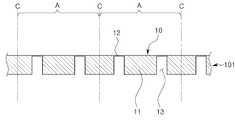
본 실시예에 따른 센서 패키지의 제조 방법은 반도체 공정(예컨대 MEMS 공정)을 이용한다. 따라서 웨이퍼 상태에서 다수 개가 일률적으로 제조되고, 제조가 완료된 후 웨이퍼를 절단하여 개별적인 센서 패키지들로 형성한다.The manufacturing method of the sensor package according to the present embodiment uses a semiconductor process (for example, a MEMS process). Accordingly, a plurality of pieces are uniformly manufactured in the wafer state, and after the manufacturing is completed, the wafer is cut into individual sensor packages.
먼저 도 3을 참조하면, 내부 공간(13)에 질량체(11)가 배치된 베이스(10)를 준비한다. 이때 질량체(11)는 연결부(도 2의 12)에 의해 베이스(10)에 연결되며, 베이스(10)의 일면에는 전극(15)과 배선 패턴(도 2의 17)이 형성된다.First, referring to FIG. 3, a base 10 in which a
전극(15)은 베이스(10)에 형성된 내부 공간(13)으로부터 일정거리 이격된 위치에 일렬로 형성될 수 있다.The
이러한 베이스(10)는 웨이퍼(wafer)와 같은 반도체 기판(101, 이하 웨이퍼)를 준비하고, 웨이퍼의 내부를 부분적으로 식각함으로써 내부 공간(13)과 질량체(11), 연결체(12) 등을 형성할 수 있다.This
한편, 하나의 웨이퍼(101)에는 다수의 베이스들(10)이 형성된다. 따라서 도 3에 도시된 바와 같이 베이스들(10)은 개별 영역(A) 별로 구분되어 하나의 웨이퍼(101) 상에 반복 배치된다.On the other hand, a plurality of
또한 절단선(C)은 후술되는 절단 공정에서 센서 패키지(1)를 개별화하기 위해 웨이퍼를 절단하는 선을 의미한다.
The cutting line C refers to a line that cuts the wafer to individualize the
이어서 도 5에 도시된 바와 같이 베이스(10)의 적어도 어느 한 면에 돌출부(19)를 형성한다. 돌출부(19)는 베이스 상에 실리콘(Si)를 증착하여 형성할 수 있다. 그러나 이에 한정되는 것은 아니다.
Then, as shown in Fig. 5,
이어서 도 6에 도시된 바와 같이 베이스(10)의 하부에 하부 캡(20)을 접합한다. 하부 캡(20)은 베이스(10)와 마찬가지로 웨이퍼(201) 상태로 준비되어 베이스(10)가 형성된 웨이퍼(101)의 하부에 접합될 수 있다.Subsequently, the
베이스(10)와 하부 캡(20)은 전술한 접합 부재(40)에 의해 접합될 수 있다. 여기서, 하부 캡 웨이퍼(201)의 일면에는 확장 홈(60)이 형성되며, 접합 부재(40)는 확장 홈(60) 내에 충진되며 베이스 웨이퍼(101)와 하부 캡 웨이퍼(201)를 상호 접합한다.
The
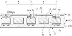
이어서 도 7에 도시된 바와 같이 상부 캡(30)을 베이스(10)에 부착한다. 상부 캡(30)도 베이스(10)와 마찬가지로 웨이퍼(301) 상태로 준비되어 베이스 웨이퍼(101)의 상부에 접합될 수 있다.Then, the
이에 웨이퍼를 적층하는 공정이 완료되며, 베이스 웨이퍼(101)의 하부와 상부에 각각 하부 캡 웨이퍼(201)와 상부 캡 웨이퍼(301)가 적층된 적층 웨이퍼가 마련된다.A stacked wafer in which the
한편 상부 캡 웨이퍼(301)에는 베이스(10)의 내부 공간(13)을 확장할 수 있는 확장 공간(33)이 식각 등을 통해 형성될 수 있다.On the other hand, the
또한, 상부 캡 웨이퍼(301)의 일면에는 확장 홈(60)이 형성되며, 접합 부재(40)는 확장 홈(60) 내에 충진되며 베이스 웨이퍼(101)와 상부 캡 웨이퍼(301)를 상호 접합한다.
An
베이스 웨이퍼(101)와 상부 캡 웨이퍼(301), 하부 캡 웨이퍼(201)는 폴리머(polymer) 재질의 접합 부재(40)에 의해 접합될 수 있다.The
폴리머 재질은 반도체 공정(예컨대 노광 공정)을 통해 패터닝이 가능하다. 따라서 반도체 공정을 통해 용이하게 접합 부재(40)를 형성할 수 있으며, 정확한 크기와 정확한 형상으로 접합 부재(40)를 도포(또는 형성)할 수 있다.The polymer material can be patterned through a semiconductor process (e.g., an exposure process). Therefore, the joining
더하여, 최적의 양으로 접합 부재(40)를 도포할 수 있으므로 실질적인 접합 과정에서 접합 부재(40)가 측면으로 과도하게 밀려나는 것도 최소화할 수 있다.In addition, since the joining
또한, 본 실시예와 같이 폴리머 재질로 접합 부재(40)를 형성하는 경우, 상대적으로 낮은 온도로 접합 공정을 수행할 수 있다. 일반적으로 폴리머의 접합 온도 200℃ 이하이다. 반면에 금속 접합 부재를 이용한 접합이나 유테틱 접합의 경우, 공정 온도는 최소 300℃ 이상이며, 일반적으로 400℃를 넘는다.Further, when the
따라서 본 제조 방법에 따르면 접합 공정에서 센서 패키지에 가해지는 열 충격을 최소화할 수 있다.Therefore, according to the present manufacturing method, thermal shock applied to the sensor package in the bonding process can be minimized.
또한 폴리머는 금속에 비해 응력이 적게 작용한다. 따라서 고온 환경과 저온 환경이 반복되는 제조 공정에서 발생하는 응력이 작으며, 베이스(10)와 캡(20, 30)의 열 팽창률이 다른 경우에는 베이스(10)와 캡(20, 30) 사이에서 완충 부재의 역할을 수행할 수 있다.The polymer also has less stress than metal. Therefore, when the
더하여, 금속 재질로 접합 부재를 형성하는 경우, 접합 부재가 배선 패턴(17)과 접촉하게 되면 단락이 발생될 수 있으므로 배선 패턴(17) 상에는 별도의 절연층이 형성되어야 한다. 또한 접합 부재가 전극(15)과 접촉하는 경우 단락이 발생될 수도 있으므로 전극(15)과 접합 부재(40) 사이의 절연 거리도 확보해야 한다.In addition, when the bonding member is formed of a metal material, a short circuit may occur when the bonding member comes into contact with the
따라서 제조 과정이 복잡하며, 센서 패키지의 크기도 증가할 수 있다.Therefore, the manufacturing process is complicated and the size of the sensor package can be increased.
그러나 본 실시예에 따른 접합 부재(40)는 폴리머 재질 즉 절연체이므로 접합 부재(40) 자체만으로 절연을 유지할 수 있으며, 전극(15)과의 이격 거리도 최소화할 수 있다.However, since the bonding
한편 본 발명의 구성은 이에 한정되지 않으며, 필요에 따라 전체적 또는 부분적으로 금속 재질의 접합 부재를 이용하는 것도 가능하다.
However, the structure of the present invention is not limited to this, and it is also possible to use a joining member made of metal wholly or in part as necessary.
다음으로, 도 8에 도시된 바와 같이, 절단선(C)을 따라 적층 웨이퍼를 절단한다. 이에 적층 웨이퍼는 개별적인 패키지들로 분리되며, 이에 도 1에 도시된 본 실시예에 따른 센서 패키지(1)가 완성된다.
Next, as shown in Fig. 8, the laminated wafer is cut along the cutting line C. Next, as shown in Fig. The laminated wafers are separated into individual packages, thereby completing the
다음으로, 상부 캡을 제조하는 방법을 설명한다.Next, a method of manufacturing the upper cap will be described.
도 9 내지 도 12는 본 실시예에 따른 캡의 제조 방법을 설명하기 위한 도면이다.9 to 12 are views for explaining a method of manufacturing a cap according to the present embodiment.
먼저 도 9를 참조하면, 상부 캡 웨이퍼(301)의 일면에 확장 홈(60)을 형성한다. 여기서 상부 캡 웨이퍼(301)로는 실리콘 기판이 이용될 수 있다.
Referring to FIG. 9, an
이어서, 도 10에 도시된 바와 같이, 확장 홈(60)이 형성된 일면에 접합 부재(40)를 형성한다.10, a joining
본 단계에서 접합 부재(40)는 확장 홈(60)에 충진되며 도포된다. 여기서 접합 부재(40)는 액상의 부재를 상기한 일면에 도포하여 형성할 수 있다.
In this step, the joining
이어서, 도 11에 도시된 바와 같이, 접합 부재(40)를 부분적으로 제거한다. 여기서 접합 부재(40)는 베이스 웨이퍼(101)와 접착되는 부분만 남겨지고 다른 부분들은 모두 제거된다.
Then, as shown in Fig. 11, the joining
이어서, 도 12에 도시된 바와 같이, 상부 캡 웨이퍼(301)를 부분적으로 제거하여 확장 공간(33)을 형성한다. 또한 확장 공간(33)들 사이에는 절단 홈(36)을 형성하여 측벽부(35)를 형성한다.Then, as shown in Fig. 12, the
이에 도 7에 도시된 상부 캡 웨이퍼(301)를 완성할 수 있다.
Thus, the
한편 본 발명은 전술한 실시예에 한정되지 않으며 다양한 변형이 가능하다.The present invention is not limited to the above-described embodiments, and various modifications are possible.
도 13은 본 발명의 다른 실시예에 따른 센서 패키지를 개략적으로 도시한 단면도이다.13 is a cross-sectional view schematically showing a sensor package according to another embodiment of the present invention.
본 실시예는 전술한 실시예의 센서 패키지(도 2의 1)와 유사하게 구성되며, 주로 접합 구조에서 차이를 갖는다. 따라서 전술한 실시예와 유사한 구성에 대해서는 설명을 생략하며, 차이를 갖는 부분에 대해서만 상세히 설명하기로 한다.This embodiment is similar to the sensor package (1 in Fig. 2) of the above-described embodiment, and mainly has a difference in the bonding structure. Therefore, the description of the configuration similar to that of the above-described embodiment will be omitted, and only the differences will be described in detail.
도 13을 참조하면, 본 실시예에 따른 센서 패키지(1a)은 베이스(10)에 전술한 돌출부(도 2의 19)가 형성되지 않는다. 그리고 돌출부가 형성된 위치에 확장부(50)가 형성된다.Referring to Fig. 13, the
확장부(50)는 접합 부재(40)의 외측에서 상부 캡(30)이나 베이스(10) 측으로 두께가 확장되는 형태로 형성되며, 접합 부재(40)에 접합되어 접합 부재(40)를 연장하는 형태로 형성될 수 있다.The
또한 확장부(50)는 접합 부재(40)와 동일한 재질로 형성되거나 다른 재질로 형성될 수 있다. 예를 들어, 확장부(50)는 수지 재질 또는 금속 재질로 형성될 수 있으며, 액상의 접착제가 응고되어 형성될 수 있다.The
이에 따라 베이스(10)나 상부 캡(30)에는 확장부(50)가 삽입 배치되는 삽입 홈(80a, 80b)이 각각 형성될 수 있다. 이때, 삽입 홈(80a, 80b)은 접합 부재(40)의 외곽을 따라 형성될 수 있다.Accordingly, the
삽입 홈(80a, 80b)은 베이스(10)와 상부 캡(30) 중 어느 하나에만 형성되거나 양쪽에 모두 형성될 수 있다.The
이러한 확장부(50)는 돌출부(19)와 마찬가지로 외력에 의해 접합 부재(40)가 파손되고 이물질이 접합 부재(40)를 관통하여 센서 패키지(1a)의 내부로 유입되는 것을 방지할 수 있다.
The
이어서 도 13에 도시된 센서 패키지의 제조 방법을 설명한다.Next, a manufacturing method of the sensor package shown in Fig. 13 will be described.
도 14 내지 도 18은 도 13에 도시된 센서 패키지의 제조 방법을 설명하기 위한 도면이다.14 to 18 are views for explaining a method of manufacturing the sensor package shown in FIG.
이를 참조하면, 먼저 도 4에 도시된 바와 같이 베이스 웨이퍼(101)가 마련되면, 도 14에 도시된 바와 같이 베이스 웨이퍼(101) 상에 삽입 홈(80b)을 형성한다. 여기서 삽입 홈(80b)은 전술한 확장부(50)가 배치되는 공간으로 이용된다.Referring to FIG. 4, when the
따라서 삽입 홈(80b)은 센서 패키지 개별 영역(A)의 경계를 따라 형성될 수 있다.
Therefore, the
이어서, 도 15에 도시된 바와 같이 하부 캡 웨이퍼(201)와 상부 캡 웨이퍼(301)를 베이스 웨이퍼(101)에 적층한다.15, the
이때, 상부 캡 웨이퍼(301)에는 전술한 확장 홈(60) 외에도 삽입 홈(80a)이 더 형성된다.At this time, the
또한 상부 캡 웨이퍼(301)에 형성된 삽입 홈(80a)은 베이스(10)에 형성된 삽입 홈(80b)과 서로 마주보는 위치에 형성된다.The
따라서 상부 캡 웨이퍼(301)가 베이스 웨이퍼(101)에 적층되면, 베이스 웨이퍼(101)와 상부 캡 웨이퍼(301)의 삽입 홈(80a, 80b)은 서로 연결되어 하나의 공간을 형성한다.When the
또한 상기한 삽입 홈들(80a, 80b)은 베이스(10)와 상부 캡(30) 사이에서 개재되는 접합 부재(40)의 외측면을 공유하며 형성된다. 따라서 상기한 공간도 접합 부재(40)의 외측면을 공유하는 공간으로 형성된다.
The
이어서 도 16에 도시된 바와 같이 하부 캡 웨이퍼(201), 베이스 웨이퍼(101), 상부 캡 웨이퍼(301)가 적층된 적층 웨이퍼를 부분 절단한다.Subsequently, as shown in Fig. 16, the laminated wafer in which the
본 단계에서 부분 절단은 절단선(C)을 따라 상부 캡 웨이퍼(301)만을 절단하는 것을 의미한다. 이에 따라, 삽입 홈들(80a, 80b)에 의해 형성된 공간은 외부와 연결된다.
In this step, partial cutting means cutting only the
이어서, 도 17에 도시된 바와 같이 삽입 홈들(80a, 80b)에 의해 형성된 공간 내에 접착제(50a)를 주입한다. 여기서 접착제(50a)는 접합 부재(40)와 동일한 재질의 접착제가 주입될 수 있다. 그러나 이에 한정되지 않으며, 접합 부재(40)와 다른 재질이더라도 상부 캡 웨이퍼(301)와 베이스 웨이퍼(101)를 상호 접합시킬 수 있는 재질이라면 다양한 재질이 이용될 수 있다.
Then, the adhesive 50a is injected into the space formed by the
이어서, 도 18에 도시된 바와 같이 절단선(C)를 따라 적층 웨이퍼를 완전히 절단한다. 이에 확장부(50)가 형성된 도 13에 도시된 센서 패키지(1a)을 완성할 수 있다.
Then, the laminated wafer is completely cut along the cutting line C as shown in Fig. Thus, the
도 19 내지 도 23은 각각 본 발명의 또 다른 실시예에 따른 센서 패키지를 개략적으로 도시한 단면도이다.19 to 23 are cross-sectional views schematically showing a sensor package according to another embodiment of the present invention, respectively.
도 19 내지 도 23를 참조하면, 전술한 실시예의 돌출부(19)나 확장부(50)를 구비하지 않는다.19 to 23, it is not provided with the projecting
도 19 내지 도 23에 도시된 접합 부재(40)는 외측으로 갈수록 두께가 두꺼워지는 형태로 형성된다.The joining
즉, 접합 부재(40)는 내부 공간과 인접한 일단의 두께보다 외부와 접하는 타단의 두께가 더 두껍게 형성된다.That is, the joining
접합 부재(40)가 이와 같이 형성되는 경우, 도 19에 도시된 바와 같이 A 방향으로 상부 캡(30)에 인가되는 힘에 대해 F 부분의 접합 부재(40)가 저항력을 제공한다. 반대로 B 방향으로 인가되는 힘에 대해 G 부분의 접합 부재(40)가 저항력을 제공한다. 따라서 돌출부(19)나 확장부(50)와 유사한 효과를 제공할 수 있다.When the joining
도 19는 상부 캡(30)의 측벽부(35) 끝단이 경사면으로 형성되는 예를 도시하고 있으며, 도 20은 측벽부(35) 끝단에 부분적으로 경사면이 형성되는 예를 도시하고 있다.FIG. 19 shows an example in which the end of the
또한 도 21은 서로 다른 경사각을 갖는 다수의 경사면으로 측벽부(35)의 끝단이 형성되는 예를 도시하고 있으며, 도 22는 측벽부(35)의 끝단이 계단 형태로 단차가 형성되는 예를 도시하고 있다. 여기서 단차는 다수개로 확장될 수 있다.21 shows an example in which the ends of the
또한 도 23은 도 20에서 경사면이 곡면으로 형성되는 경우를 도시하고 있다.Fig. 23 shows a case in which the inclined surface is formed as a curved surface in Fig.
본 실시예들에 따른 센서 패키지들은 도 19에 도시된 바와 같이 내측에서 외측으로 갈수록 점진적으로 두께가 증가하는 형태로 접합 부재가 형성될 수 있다. 또한 도 20 내지 도 23에 도시된 바와 같이, 내측에서 외측으로 갈 때 두께가 급격히 증가하는 지점을 적어도 하나 포함하는 형태로 접합 부재가 형성될 수 있다.As shown in FIG. 19, the sensor packages according to the present embodiments may be formed in such a manner that the thickness gradually increases from the inside to the outside. As shown in FIGS. 20 to 23, the joining member may be formed to include at least one point where the thickness increases sharply from the inside to the outside.
이처럼 본 실시예에 따른 센서 패키지는 다양한 변형이 가능하다.
As described above, the sensor package according to the present embodiment can be variously modified.
이상에서 본 발명의 실시예들에 대하여 상세하게 설명하였지만 본 발명의 권리범위는 이에 한정되는 것은 아니고, 청구범위에 기재된 본 발명의 기술적 사상을 벗어나지 않는 범위 내에서 다양한 수정 및 변형이 가능하다는 것은 당 기술분야의 통상의 지식을 가진 자에게는 자명할 것이다.
While the present invention has been particularly shown and described with reference to exemplary embodiments thereof, it is to be understood that the scope of the invention is not limited to the disclosed exemplary embodiments, but, on the contrary, is intended to cover various modifications and equivalent arrangements included within the spirit and scope of the appended claims. And will be apparent to those skilled in the art.
100: 센서 모듈
1, 1a: 센서 패키지
10: 베이스
19: 돌출부
20: 하부 캡
30: 상부 캡
40: 접합 부재
50: 확장부
60: 확장 홈100: Sensor module
1, 1a: sensor package
10: Base
19:
20: Lower cap
30: upper cap
40:
50: Extension part
60: Extended groove
Claims (20)
Translated fromKorean상기 베이스의 일면에 결합되어 상기 질량체가 배치된 공간을 밀봉하는 적어도 하나의 캡; 및
상기 베이스와 상기 캡을 상호 접합하는 접합 부재;
를 포함하며,
상기 캡은 상기 접합 부재가 접합되는 접합면에 적어도 하나의 확장 홈이 형성되고, 상기 접합 부재는 상기 확장 홈에 충진되는 센서 패키지.
A base having a mass disposed therein;
At least one cap coupled to one surface of the base to seal a space in which the mass is disposed; And
A joining member for joining the base and the cap to each other;
/ RTI >
Wherein the cap has at least one extending groove formed in a joint surface to which the joining member is joined, and the joining member is filled in the extending groove.
편평한 면을 갖는 면부와 상기 면부에서 상기 베이스 측으로 연장되는 측벽부를 포함하며, 상기 확장 홈은 상기 측벽부의 끝단에 형성되는 센서 패키지.
2. The cap according to claim 1,
And a side wall portion extending from the surface portion to the base side, wherein the extending groove is formed at an end of the side wall portion.
상기 캡이 접합되는 일면에서 상기 측벽부의 외곽을 따라 돌출되는 돌출부를 포함하는 센서 패키지.
3. The apparatus of claim 2,
And protrusions protruding along an outer periphery of the side wall portion on one side where the cap is joined.
상기 접합 부재의 두께와 동일하거나, 상기 접합 부재의 두께 보다 더 길게 돌출되는 센서 패키지.
4. The apparatus of claim 3, wherein the protrusions
Wherein the thickness of the bonding member is equal to or greater than the thickness of the bonding member.
상기 접합 부재의 두께를 확장하는 형태로 형성되어 상기 접합 부재의 외곽을 따라 배치되는 확장부를 더 포함하는 센서 패키지.
The method according to claim 1,
Further comprising an extension portion formed to expand the thickness of the joining member and disposed along an outer periphery of the joining member.
상기 확장부가 삽입 배치되는 삽입 홈을 적어도 하나 구비하는 센서 패키지.
6. The apparatus of claim 5, wherein at least one of the cap or the base comprises:
And at least one insertion groove into which the extension portion is inserted.
상기 접합 부재와 동일한 재질로 형성되는 센서 패키지.
6. The apparatus of claim 5,
Wherein the connection member is made of the same material as the bonding member.
상기 접합 부재에 접합되어 상기 접합 부재와 일체로 형성되는 센서 패키지.
6. The apparatus of claim 5,
And a sensor package joined to the bonding member and formed integrally with the bonding member.
상기 베이스의 일면에 결합되어 상기 질량체가 배치된 공간을 밀봉하는 적어도 하나의 캡; 및
상기 베이스와 상기 캡을 상호 접합하는 접합 부재;
를 포함하며,
상기 접합 부재는 내측과 외측의 두께가 다르게 형성되는 센서 패키지.
A base having a mass disposed therein;
At least one cap coupled to one surface of the base to seal a space in which the mass is disposed; And
A joining member for joining the base and the cap to each other;
/ RTI >
Wherein the bonding member has a thickness different from that of the inside and the outside.
외측의 두께가 내측에 비해 더 두껍게 형성되는 센서 패키지.
10. The image forming apparatus according to claim 9, wherein the joining member
And the thickness of the outer side is formed thicker than that of the inner side.
내측에서 외측으로 갈수록 점진적으로 두께가 증가하는 센서 패키지.
The joining member according to claim 10,
The sensor package has a gradually increasing thickness from the inner side to the outer side.
내측에서 외측으로 갈 때 두께가 급격히 증가하는 지점을 적어도 하나 포함하는 센서 패키지.
The joining member according to claim 10,
And at least one point where the thickness increases sharply from the inside to the outside.
접합 부재를 매개로 하여 접합면에 확장 홈이 형성된 캡을 상기 베이스에 접합하는 단계;
를 포함하는 센서 패키지 제조 방법.
Preparing a base having a mass; And
Joining a cap having an enlarged groove on a joint surface to the base via a joining member;
≪ / RTI >
상기 접합 부재를 상기 확장 홈에 충진하는 단계를 포함하는 센서 패키지 제조 방법.
14. The method of claim 13, wherein bonding the cap to the base comprises:
And filling the joining member into the expansion groove.
상기 캡이 접합되는 상기 접합면에 돌출부가 형성된 베이스를 준비하는 단계인 센서 패키지 제조 방법.
15. The method of claim 14, wherein preparing the base comprises:
And preparing a base having a protruding portion formed on the bonding surface to which the cap is bonded.
상기 접합면에 접합된 상기 캡의 외곽을 따라 돌출되는 센서 패키지 제조 방법.
16. The apparatus according to claim 15,
And protruding along an outer periphery of the cap joined to the joint surface.
상기 접합 부재의 두께에 대응하는 거리로 돌출되는 센서 패키지 제조 방법.
17. The apparatus of claim 16,
And protruding at a distance corresponding to the thickness of the joining member.
접합 부재를 매개로 하여 상기 베이스의 일면에 캡 웨이퍼를 접합하는 단계;
상기 캡 웨이퍼를 절단하여 상기 삽입 홈을 노출시키는 단계;
상기 삽입 홈에 접착제를 주입하여 확장부를 형성하는 단계; 및
상기 베이스 웨이퍼를 절단하는 단계;
를 포함하는 센서 패키지 제조 방법.
Preparing a base wafer having a plurality of mass bodies and having at least one insertion groove formed on one surface thereof;
Joining a cap wafer to one surface of the base via a joining member;
Exposing the insert groove by cutting the cap wafer;
Injecting an adhesive into the insertion groove to form an extended portion; And
Cutting the base wafer;
≪ / RTI >
상기 접합 부재가 접합되는 접합면에 적어도 하나의 확장 홈이 형성된 캡 웨이퍼를 준비하는 단계; 및
상기 접합 부재를 상기 확장 홈에 충진하는 단계;
를 포함하는 센서 패키지 제조 방법.
19. The method of claim 18, wherein bonding the cap wafer comprises:
Preparing a cap wafer having at least one extending groove formed on a joint surface to which the joining member is joined; And
Filling the joining member into the extension groove;
≪ / RTI >
상기 접합 부재의 외곽을 따라 상기 삽입 홈이 형성된 베이스 웨이퍼를 준비하는 단계인 센서 패키지 제조 방법.
19. The method of claim 18, wherein preparing the base wafer comprises:
And preparing a base wafer having the insertion groove formed along an outer periphery of the joining member.
Priority Applications (1)
| Application Number | Priority Date | Filing Date | Title |
|---|---|---|---|
| KR1020140177557AKR20160070514A (en) | 2014-12-10 | 2014-12-10 | Sensor package and manufacturing method thereof |
Applications Claiming Priority (1)
| Application Number | Priority Date | Filing Date | Title |
|---|---|---|---|
| KR1020140177557AKR20160070514A (en) | 2014-12-10 | 2014-12-10 | Sensor package and manufacturing method thereof |
Publications (1)
| Publication Number | Publication Date |
|---|---|
| KR20160070514Atrue KR20160070514A (en) | 2016-06-20 |
Family
ID=56354341
Family Applications (1)
| Application Number | Title | Priority Date | Filing Date |
|---|---|---|---|
| KR1020140177557AWithdrawnKR20160070514A (en) | 2014-12-10 | 2014-12-10 | Sensor package and manufacturing method thereof |
Country Status (1)
| Country | Link |
|---|---|
| KR (1) | KR20160070514A (en) |
Cited By (1)
| Publication number | Priority date | Publication date | Assignee | Title |
|---|---|---|---|---|
| KR20180029654A (en)* | 2016-09-13 | 2018-03-21 | (주)포인트엔지니어링 | Micro sensor package |
Citations (1)
| Publication number | Priority date | Publication date | Assignee | Title |
|---|---|---|---|---|
| JP2001337105A (en) | 2000-05-26 | 2001-12-07 | Matsushita Electric Works Ltd | Semiconductor acceleration sensor |
- 2014
- 2014-12-10KRKR1020140177557Apatent/KR20160070514A/ennot_activeWithdrawn
Patent Citations (1)
| Publication number | Priority date | Publication date | Assignee | Title |
|---|---|---|---|---|
| JP2001337105A (en) | 2000-05-26 | 2001-12-07 | Matsushita Electric Works Ltd | Semiconductor acceleration sensor |
Cited By (2)
| Publication number | Priority date | Publication date | Assignee | Title |
|---|---|---|---|---|
| KR20180029654A (en)* | 2016-09-13 | 2018-03-21 | (주)포인트엔지니어링 | Micro sensor package |
| KR101868833B1 (en)* | 2016-09-13 | 2018-06-20 | (주)포인트엔지니어링 | Micro sensor package |
Similar Documents
| Publication | Publication Date | Title |
|---|---|---|
| US9818665B2 (en) | Method of packaging a semiconductor chip using a 3D printing process and semiconductor package having angled surfaces | |
| US9670057B1 (en) | Sensor device and method for making thereof | |
| KR101015726B1 (en) | Semiconductor device and electronic device manufacturing method | |
| US9735128B2 (en) | Method for incorporating stress sensitive chip scale components into reconstructed wafer based modules | |
| US20120086113A1 (en) | Flexible circuits and methods for making the same | |
| US20100055841A1 (en) | Semiconductor device and method of producing the same | |
| US10800651B2 (en) | Low stress integrated device packages | |
| US8164180B2 (en) | Functional element package and fabrication method therefor | |
| JP2016149539A (en) | Packaged microchip with patterned interposer | |
| US7911043B2 (en) | Wafer level device package with sealing line having electroconductive pattern and method of packaging the same | |
| CN110573840B (en) | Sensor package | |
| JP4675945B2 (en) | Semiconductor device | |
| KR102004797B1 (en) | Sensor package and manufacturing method thereof | |
| JP6730948B2 (en) | Optical device and manufacturing method thereof | |
| KR20160070514A (en) | Sensor package and manufacturing method thereof | |
| CN214990262U (en) | Semiconductor device with a plurality of semiconductor chips | |
| JP2006351590A (en) | Substrate with built-in microdevice, and its manufacturing method | |
| US11430765B2 (en) | Semiconductor sensor package | |
| JP6007535B2 (en) | Hollow sealing structure and hollow package including the same | |
| EP3573095B1 (en) | A sensor package and a method of manufacturing a sensor package | |
| JP2007042786A (en) | Micro device and its packaging method | |
| KR102409479B1 (en) | Wafer level hermetic package manufacturing method | |
| JP2005224925A (en) | Micro-package and method of manufacturing the same | |
| KR20160135528A (en) | Sensor package and manufacturing method thereof | |
| KR20130095489A (en) | Micro electro mechanical systems package |
Legal Events
| Date | Code | Title | Description |
|---|---|---|---|
| PA0109 | Patent application | Patent event code:PA01091R01D Comment text:Patent Application Patent event date:20141210 | |
| PG1501 | Laying open of application | ||
| PC1203 | Withdrawal of no request for examination | ||
| WITN | Application deemed withdrawn, e.g. because no request for examination was filed or no examination fee was paid |