KR20160069093A - Clock and data recovery circuit and system using the same - Google Patents
Clock and data recovery circuit and system using the sameDownload PDFInfo
- Publication number
- KR20160069093A KR20160069093AKR1020140174449AKR20140174449AKR20160069093AKR 20160069093 AKR20160069093 AKR 20160069093AKR 1020140174449 AKR1020140174449 AKR 1020140174449AKR 20140174449 AKR20140174449 AKR 20140174449AKR 20160069093 AKR20160069093 AKR 20160069093A
- Authority
- KR
- South Korea
- Prior art keywords
- signal
- phase
- clock signal
- data
- clock
- Prior art date
- Legal status (The legal status is an assumption and is not a legal conclusion. Google has not performed a legal analysis and makes no representation as to the accuracy of the status listed.)
- Withdrawn
Links
- 238000011084recoveryMethods0.000titleclaimsabstractdescription18
- 238000001914filtrationMethods0.000claimsabstractdescription39
- 238000000034methodMethods0.000claimsdescription15
- 230000000630rising effectEffects0.000claimsdescription6
- 238000001514detection methodMethods0.000description25
- 238000010586diagramMethods0.000description12
- 230000005540biological transmissionEffects0.000description9
- 230000007704transitionEffects0.000description9
- 230000003111delayed effectEffects0.000description4
- 238000004891communicationMethods0.000description1
- 238000012986modificationMethods0.000description1
- 230000004048modificationEffects0.000description1
- 239000004065semiconductorSubstances0.000description1
Images


Classifications
- H—ELECTRICITY
- H04—ELECTRIC COMMUNICATION TECHNIQUE
- H04L—TRANSMISSION OF DIGITAL INFORMATION, e.g. TELEGRAPHIC COMMUNICATION
- H04L7/00—Arrangements for synchronising receiver with transmitter
- H04L7/02—Speed or phase control by the received code signals, the signals containing no special synchronisation information
- H04L7/033—Speed or phase control by the received code signals, the signals containing no special synchronisation information using the transitions of the received signal to control the phase of the synchronising-signal-generating means, e.g. using a phase-locked loop
- G—PHYSICS
- G11—INFORMATION STORAGE
- G11C—STATIC STORES
- G11C7/00—Arrangements for writing information into, or reading information out from, a digital store
- G11C7/22—Read-write [R-W] timing or clocking circuits; Read-write [R-W] control signal generators or management
- G11C7/222—Clock generating, synchronizing or distributing circuits within memory device
- G—PHYSICS
- G11—INFORMATION STORAGE
- G11C—STATIC STORES
- G11C7/00—Arrangements for writing information into, or reading information out from, a digital store
- G11C7/10—Input/output [I/O] data interface arrangements, e.g. I/O data control circuits, I/O data buffers
- G11C7/1051—Data output circuits, e.g. read-out amplifiers, data output buffers, data output registers, data output level conversion circuits
- G11C7/1063—Control signal output circuits, e.g. status or busy flags, feedback command signals
- G—PHYSICS
- G11—INFORMATION STORAGE
- G11C—STATIC STORES
- G11C7/00—Arrangements for writing information into, or reading information out from, a digital store
- G11C7/10—Input/output [I/O] data interface arrangements, e.g. I/O data control circuits, I/O data buffers
- G11C7/1072—Input/output [I/O] data interface arrangements, e.g. I/O data control circuits, I/O data buffers for memories with random access ports synchronised on clock signal pulse trains, e.g. synchronous memories, self timed memories
- G—PHYSICS
- G11—INFORMATION STORAGE
- G11C—STATIC STORES
- G11C7/00—Arrangements for writing information into, or reading information out from, a digital store
- G11C7/10—Input/output [I/O] data interface arrangements, e.g. I/O data control circuits, I/O data buffers
- G11C7/1078—Data input circuits, e.g. write amplifiers, data input buffers, data input registers, data input level conversion circuits
- G11C7/109—Control signal input circuits
- G—PHYSICS
- G11—INFORMATION STORAGE
- G11C—STATIC STORES
- G11C7/00—Arrangements for writing information into, or reading information out from, a digital store
- G11C7/22—Read-write [R-W] timing or clocking circuits; Read-write [R-W] control signal generators or management
- G11C7/225—Clock input buffers
- H—ELECTRICITY
- H03—ELECTRONIC CIRCUITRY
- H03L—AUTOMATIC CONTROL, STARTING, SYNCHRONISATION OR STABILISATION OF GENERATORS OF ELECTRONIC OSCILLATIONS OR PULSES
- H03L7/00—Automatic control of frequency or phase; Synchronisation
- H03L7/06—Automatic control of frequency or phase; Synchronisation using a reference signal applied to a frequency- or phase-locked loop
- H03L7/08—Details of the phase-locked loop
- H03L7/0807—Details of the phase-locked loop concerning mainly a recovery circuit for the reference signal
- H—ELECTRICITY
- H03—ELECTRONIC CIRCUITRY
- H03L—AUTOMATIC CONTROL, STARTING, SYNCHRONISATION OR STABILISATION OF GENERATORS OF ELECTRONIC OSCILLATIONS OR PULSES
- H03L7/00—Automatic control of frequency or phase; Synchronisation
- H03L7/06—Automatic control of frequency or phase; Synchronisation using a reference signal applied to a frequency- or phase-locked loop
- H03L7/08—Details of the phase-locked loop
- H03L7/081—Details of the phase-locked loop provided with an additional controlled phase shifter
- H03L7/0812—Details of the phase-locked loop provided with an additional controlled phase shifter and where no voltage or current controlled oscillator is used
- H03L7/0814—Details of the phase-locked loop provided with an additional controlled phase shifter and where no voltage or current controlled oscillator is used the phase shifting device being digitally controlled
- H—ELECTRICITY
- H03—ELECTRONIC CIRCUITRY
- H03L—AUTOMATIC CONTROL, STARTING, SYNCHRONISATION OR STABILISATION OF GENERATORS OF ELECTRONIC OSCILLATIONS OR PULSES
- H03L7/00—Automatic control of frequency or phase; Synchronisation
- H03L7/06—Automatic control of frequency or phase; Synchronisation using a reference signal applied to a frequency- or phase-locked loop
- H03L7/08—Details of the phase-locked loop
- H03L7/081—Details of the phase-locked loop provided with an additional controlled phase shifter
- H03L7/0812—Details of the phase-locked loop provided with an additional controlled phase shifter and where no voltage or current controlled oscillator is used
- H03L7/0816—Details of the phase-locked loop provided with an additional controlled phase shifter and where no voltage or current controlled oscillator is used the controlled phase shifter and the frequency- or phase-detection arrangement being connected to a common input
- H—ELECTRICITY
- H03—ELECTRONIC CIRCUITRY
- H03L—AUTOMATIC CONTROL, STARTING, SYNCHRONISATION OR STABILISATION OF GENERATORS OF ELECTRONIC OSCILLATIONS OR PULSES
- H03L7/00—Automatic control of frequency or phase; Synchronisation
- H03L7/06—Automatic control of frequency or phase; Synchronisation using a reference signal applied to a frequency- or phase-locked loop
- H03L7/08—Details of the phase-locked loop
- H03L7/085—Details of the phase-locked loop concerning mainly the frequency- or phase-detection arrangement including the filtering or amplification of its output signal
- H03L7/087—Details of the phase-locked loop concerning mainly the frequency- or phase-detection arrangement including the filtering or amplification of its output signal using at least two phase detectors or a frequency and phase detector in the loop
- H—ELECTRICITY
- H03—ELECTRONIC CIRCUITRY
- H03L—AUTOMATIC CONTROL, STARTING, SYNCHRONISATION OR STABILISATION OF GENERATORS OF ELECTRONIC OSCILLATIONS OR PULSES
- H03L7/00—Automatic control of frequency or phase; Synchronisation
- H03L7/06—Automatic control of frequency or phase; Synchronisation using a reference signal applied to a frequency- or phase-locked loop
- H03L7/08—Details of the phase-locked loop
- H03L7/085—Details of the phase-locked loop concerning mainly the frequency- or phase-detection arrangement including the filtering or amplification of its output signal
- H03L7/089—Details of the phase-locked loop concerning mainly the frequency- or phase-detection arrangement including the filtering or amplification of its output signal the phase or frequency detector generating up-down pulses
- H03L7/0891—Details of the phase-locked loop concerning mainly the frequency- or phase-detection arrangement including the filtering or amplification of its output signal the phase or frequency detector generating up-down pulses the up-down pulses controlling source and sink current generators, e.g. a charge pump
- H03L7/0895—Details of the current generators
- H03L7/0896—Details of the current generators the current generators being controlled by differential up-down pulses
- H—ELECTRICITY
- H04—ELECTRIC COMMUNICATION TECHNIQUE
- H04L—TRANSMISSION OF DIGITAL INFORMATION, e.g. TELEGRAPHIC COMMUNICATION
- H04L5/00—Arrangements affording multiple use of the transmission path
- H04L5/003—Arrangements for allocating sub-channels of the transmission path
- H04L5/0053—Allocation of signalling, i.e. of overhead other than pilot signals
- H—ELECTRICITY
- H04—ELECTRIC COMMUNICATION TECHNIQUE
- H04L—TRANSMISSION OF DIGITAL INFORMATION, e.g. TELEGRAPHIC COMMUNICATION
- H04L7/00—Arrangements for synchronising receiver with transmitter
- H04L7/02—Speed or phase control by the received code signals, the signals containing no special synchronisation information
- H04L7/033—Speed or phase control by the received code signals, the signals containing no special synchronisation information using the transitions of the received signal to control the phase of the synchronising-signal-generating means, e.g. using a phase-locked loop
- H04L7/0337—Selecting between two or more discretely delayed clocks or selecting between two or more discretely delayed received code signals
Landscapes
- Engineering & Computer Science (AREA)
- Computer Networks & Wireless Communication (AREA)
- Signal Processing (AREA)
- Synchronisation In Digital Transmission Systems (AREA)
Abstract
Translated fromKoreanDescription
Translated fromKorean본 발명은 반도체 장치에 관한 것으로서, 더 상세하게는 클럭 데이터 리커버리 회로 및 이를 이용하는 시스템에 관한 것이다.The present invention relates to semiconductor devices, and more particularly, to a clock data recovery circuit and a system using the same.
일반적으로 적은 개수의 데이터 버스를 통해 직렬 데이터 통신을 하는 시스템은 클럭 데이터 리커버리 방식을 사용한다. 상기 클럭 데이터 리커버리 방식은 직렬 데이터로부터 기준이 되는 클럭 신호를 생성하고, 생성된 클럭 신호를 데이터를 수신하기 위한 스트로브 신호로 사용한다. 따라서, 전송 장치는 상기 클럭 신호와 관련된 정보를 갖는 데이터를 전송할 수 있고, 수신 장치는 상기 데이터로부터 클럭 신호를 생성한 후 생성된 클럭 신호에 동기하여 상기 전송 장치로부터 전송된 데이터를 수신할 수 있다.Generally, a system that performs serial data communication over a small number of data buses uses a clock data recovery scheme. The clock data recovery scheme generates a reference clock signal from the serial data, and uses the generated clock signal as a strobe signal for receiving data. Thus, the transmitting apparatus can transmit data having information related to the clock signal, and the receiving apparatus can receive the data transmitted from the transmitting apparatus in synchronization with the clock signal generated after generating the clock signal from the data .
노이즈와 지터 등에 의해 신호 왜곡을 최소화하고 데이터 유효 윈도우를 증가시키기 위해, 상기 수신 장치는 데이터로부터 생성된 클럭 신호의 위상과 데이터의 천이 시점을 비교하여 상기 클럭의 신호의 위상을 조절할 수 있다.In order to minimize signal distortion due to noise and jitter and to increase the data effective window, the receiving device can adjust the phase of the clock signal by comparing the phase of the clock signal generated from the data with the transition timing of the data.
본 발명의 실시예는 클럭 신호의 위상 정보 획득은 짧은 주기로 수행되고, 상기 클럭 신호의 위상의 조절은 보다 긴 주기로 수행될 수 있는 클럭 데이터 리커버리 회로를 제공할 수 있다.The embodiment of the present invention can provide a clock data recovery circuit in which the phase information acquisition of the clock signal is performed in a short cycle and the adjustment of the phase of the clock signal can be performed in a longer cycle.
본 발명의 실시예에 따른 클럭 데이터 리커버리 회로는 클럭 신호와 데이터를 비교하여 얼리 위상 감지 신호 및 레이트 위상 감지 신호를 생성하는 위상 검출부; 상기 얼리 위상 감지 신호의 생성 횟수와 상기 레이트 위상 감지 신호의 생성 횟수에 따라 업 신호 및 다운 신호를 생성하는 필터링부; 상기 클럭 신호의 주기마다 상기 필터링부의 출력을 수신하고, 상기 클럭 신호의 주기의 n 배 (n은 2이상의 정수)에 해당하는 합산 시간 동안 상기 필터링부로부터 수신된 상기 업 신호 및 상기 다운 신호의 개수를 합산하여 제 1 및 제 2 위상 제어 신호를 생성하는 위상 정보 합산부; 및 상기 제 1 및 제 2 위상 제어 신호에 응답하여 상기 클럭 신호의 위상을 조절하는 위상 보간기를 포함할 수 있다.A clock data recovery circuit according to an embodiment of the present invention includes: a phase detector for generating an early phase sense signal and a rate phase sense signal by comparing a clock signal and data; A filtering unit for generating an up signal and a down signal according to the number of generation of the early phase sense signal and the number of generation of the rate phase sense signal; And the number of the up signal and the down signal received from the filtering unit during a summation time corresponding to n times (n is an integer equal to or greater than 2) times the period of the clock signal, A phase information summation unit for generating first and second phase control signals; And a phase interpolator for adjusting the phase of the clock signal in response to the first and second phase control signals.
본 발명의 실시예에 따른 클럭 데이터 리커버리 회로는 제 1 클럭 신호와 데이터를 비교하여 얼리 위상 감지 신호 및 레이트 위상 감지 신호를 생성하는 위상 검출부; 상기 얼리 위상 감지 신호의 생성 횟수와 상기 레이트 위상 감지 신호의 생성 횟수에 따라 업 신호 및 다운 신호를 생성하는 필터링부; 상기 제 1 클럭 신호에 동기하여 상기 업 신호 및 상기 다운 신호의 생성 횟수를 합산하고, 합산된 결과를 제 2 클럭 신호에 동기하여 제 1 및 제 2 위상 제어 신호로서 출력하는 위상 정보 합산부; 및 상기 제 2 클럭 신호에 동기하여 업데이트될 때 상기 제 1 및 제 2 위상 제어 신호에 기초하여 상기 제 1 클럭 신호의 위상을 보정하는 위상 보간기를 포함할 수 있다.A clock data recovery circuit according to an embodiment of the present invention includes: a phase detector for comparing a first clock signal with data to generate an early phase sense signal and a rate phase sense signal; A filtering unit for generating an up signal and a down signal according to the number of generation of the early phase sense signal and the number of generation of the rate phase sense signal; A phase information summation unit for summing up the number of times of generation of the up signal and the down signal in synchronization with the first clock signal and for outputting the summed result as first and second phase control signals in synchronization with the second clock signal; And a phase interpolator that corrects the phase of the first clock signal based on the first and second phase control signals when updated in synchronization with the second clock signal.
본 발명의 실시예는 수신되는 데이터의 신호 무결성을 향상시키면서 시스템의 전력 소모를 감소시킬 수 있다.Embodiments of the present invention can reduce the power consumption of the system while improving the signal integrity of the received data.
도 1은 본 발명의 실시예에 따른 시스템의 구성을 보여주는 도면,
도 2는 본 발명의 실시예에 따른 클럭 데이터 리커버리 회로의 구성을 보여주는 도면,
도 3a 내지 3d는 도 2에 도시된 위상 검출부의 동작을 보여주는 타이밍도 및 테이블,
도 4는 도 2에 도시된 위상 정보 합산부의 개략적인 구성을 보여주는 블록도,
도 5는 도 4에 도시된 업 신호 합산기의 구성을 보여주는 도면,
도 6은 도 5에 도시된 업 신호 합산기의 동작을 보여주는 타이밍도이다.BRIEF DESCRIPTION OF THE DRAWINGS FIG. 1 is a block diagram of a system according to an embodiment of the present invention; FIG.
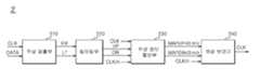
FIG. 2 is a diagram illustrating a configuration of a clock data recovery circuit according to an embodiment of the present invention;
FIGS. 3A to 3D are timing diagrams and tables showing the operation of the phase detector shown in FIG. 2,
FIG. 4 is a block diagram showing a schematic configuration of the phase information summation unit shown in FIG. 2;
FIG. 5 is a diagram showing the configuration of the up-signal adder shown in FIG. 4,
6 is a timing diagram showing the operation of the up signal summer shown in Fig.
도 1에서, 본 발명의 실시예에 따른 시스템(1)의 구성을 보여주는 도면이다. 도 1에서, 상기 시스템(1)은 전송 장치(110) 및 수신 장치(120)를 포함할 수 있다. 상기 전송 장치(110)는 데이터를 전송하는 쪽을 대표하는 구성요소일 수 있고, 상기 수신 장치(120)는 상기 전송 장치(110)로부터 전송된 데이터를 수신하는 쪽을 대표하는 구성요소일 수 있다. 예를 들어, 상기 시스템(1)은 마스터 장치와 슬레이브 장치를 포함할 수 있고, 마스터 장치로부터 상기 슬레이브 장치로 데이터가 전송될 때, 상기 마스터 장치는 상기 전송 장치(110)일 수 있고, 상기 슬레이브 장치는 상기 수신 장치(120)일 수 있다. 반대로, 상기 슬레이브 장치로부터 상기 마스터 장치로 데이터가 전송될 때, 상기 마스터 장치는 상기 수신 장치(120)일 수 있고, 상기 슬레이브 장치는 상기 전송 장치(110)일 수 있다.1 is a diagram showing the configuration of a
상기 시스템(1)을 구성하는 상기 전송 장치(110) 및 상기 수신 장치(120)는 적은 개수의 데이터 버스를 사용하는 직렬 데이터 전송 방식으로 통신할 수 있다. 도 1에서, 상기 전송 장치(110)는 데이터 인코더(111)를 포함할 수 있다. 상기 수신 장치(120)는 클럭 데이터 리커버리 회로(121, CDR) 및 데이터 디코더(122)를 포함할 수 있다. 상기 전송 장치(110)는 복수의 데이터 버스(131, 132, 133)를 통해 상기 수신 장치(120)와 연결될 수 있다. 도 1에서, 상기 데이터 버스(131, 132, 133)의 개수는 3개인 것으로 예시하였으나, 이에 한정하려는 의도는 아니다. 상기 전송 장치(110)는 상기 데이터 인코더(111)를 통해 적어도 4비트 이상의 내부 데이터를 인코딩하여 복수 그룹의 3비트의 데이터(D1, D2, D3)로 변환할 수 있다. 상기 복수 그룹의 3비트 데이터(D1, D2, D3)는 상기 데이터 버스(131, 132, 133)를 통해 순차적으로 직렬 전송될 수 있다. 상기 데이터(D1, D2, D3)는 상기 데이터 버스(131, 132, 133)를 통해 전송되는 데이터를 지칭할 수 있고, 상기 내부 데이터는 상기 전송 장치(110) 또는 상기 수신 장치(120) 내부에서 사용되는 데이터를 지칭할 수 있다. 예를 들어, 상기 데이터 인코더(111)는 16비트의 내부 데이터를 인코딩하여 7개 그룹의 3비트 데이터(D1, D2, D3)로 변환할 수 있고, 상기 7개 그룹의 3비트 데이터(D1, D2, D3)는 상기 3개의 데이터 버스(131, 132, 133)를 통해 직렬 전송될 수 있다.The
상기 수신 장치(120)의 클럭 데이터 리커버리 회로(121, CDR)는 상기 데이터 버스(131, 132, 133)를 통해 전송된 데이터로부터 클럭 신호(CLK)를 생성할 수 있다. 상기 클럭 신호(CLK)는 스트로브 신호로 사용될 수 있고, 상기 수신 장치(120)는 상기 클럭 신호(CLK)에 동기하여 상기 데이터 버스(131, 132, 133)를 통해 전송된 데이터(D1, D2, D3)를 수신할 수 있다. 상기 데이터 디코더(122)는 상기 데이터 버스(131, 132, 133)를 통해 전송된 복수 그룹의 3비트 데이터(D1, D2, D3)를 적어도 4비트 이상의 내부 데이터로 변환할 수 있다. 예를 들어, 상기 데이터 디코더(122)는 3비트씩 7회에 걸쳐 순차적으로 전송된 21비트의 데이터(D1, D2, D3)를 디코딩하여 16비트의 내부 데이터로 변환할 수 있다.The clock
상기 데이터 인코더(111) 및 상기 데이터 디코더(122)는 상기 내부 데이터를 상기 데이터(D1, D2, D3)로 변환하거나 상기 데이터(D1, D2, D3)를 상기 내부 데이터로 변환하기 위한 변환 테이블을 포함할 수 있다. 상기 3개의 데이터 버스(131, 132, 133)를 통해 전송되는 3비트의 데이터(D1, D2, D3)는 3개의 상태(phase, state 또는 level)를 갖는 데이터일 수 있다.The
상기 클럭 데이터 리커버리 회로(121)는 상기 데이터(D1, D2, D3)로부터 클럭 신호(CLK)를 생성할 수 있고, 상기 클럭 신호(CLK)와 상기 데이터(D1, D2, D3)를 비교하여 상기 클럭 신호(CLK)의 위상을 조절할 수 있다.The clock
도 2는 본 발명의 실시예에 따른 클럭 데이터 리커버리 회로(2)의 구성을 보여주는 도면이다. 도 2에서, 상기 클럭 데이터 리커버리 회로(2)는 위상 검출부(210), 필터링부(220), 위상 정보 합산부(230) 및 위상 보간기(240)를 포함할 수 있다. 상기 위상 검출부(210)는 클럭 신호(CLK) 및 데이터(DATA)를 수신하고, 상기 클럭 신호(CLK)의 주기마다 상기 클럭 신호(CLK)와 상기 데이터(DATA)를 비교할 수 있다. 예를 들어, 상기 위상 검출부(210)는 상기 클럭 신호(CLK)의 에지가 상기 데이터(DATA)의 천이 시점에 비해 앞서있는지 뒤져있는지 여부를 검출할 수 있다. 상기 위상 검출부(210)는 상기 클럭 신호(CLK)와 상기 데이터(DATA)를 비교하여 얼리 위상 감지 신호(ER) 및 레이트 위상 감지 신호(LT)를 생성할 수 있다. 예를 들어, 상기 위상 검출부(210)는 상기 데이터(DATA)의 천이 시점에 비해 상기 클럭 신호(CLK)의 에지가 앞서 있으면 상기 얼리 위상 감지 신호(ER)를 생성할 수 있고, 상기 데이터(DATA)의 천이 시점에 비해 상기 클럭 신호(CLK)의 에지가 뒤져 있으면 상기 레이트 위상 감지 신호(LT)를 생성할 수 있다. 상기 위상 검출부(210)의 구체적인 동작에 대해서는 후술하기로 한다.2 is a diagram showing a configuration of a clock
상기 필터링부(220)는 상기 위상 검출부(210)로부터 상기 얼리 위상 감지 신호(ER) 및 상기 레이트 위상 감지 신호(LT)를 수신하고, 업 신호(UP) 및 다운 신호(DN)를 생성할 수 있다. 상기 필터링부(220)는 상기 얼리 위상 감지 신호의(ER) 생성 횟수와 상기 레이트 위상 감지 신호(LT)의 생성 횟수에 따라 상기 업 신호(UP) 및 상기 다운 신호(DN)를 생성할 수 있다. 상기 필터링부(220)는 상기 얼리 위상 감지 신호(ER)의 생성 횟수와 상기 레이트 위상 감지 신호(LT)의 생성 횟수의 차이가 소정 개수에 도달했을 때, 상기 업 신호(UP) 및 상기 다운 신호(DN) 중 하나를 생성할 수 있다. 상시 소정 개수는 상기 필터링부(220)의 필터 길이(filter depth)에 대응할 수 있다. 예를 들어, 상기 필터 길이가 3이라면, 상기 필터링부(220)는 상기 얼리 위상 감지 신호(ER)가 상기 레이트 위상 감지 신호(LT)보다 3회 더 많이 생성되었을 때 상기 다운 신호(DN)를 생성할 수 있다. 또한, 상기 필터링부(220)는 상기 레이트 위상 감지 신호(LT)가 상기 얼리 위상 감지 신호(ER)보다 3회 더 많이 생성되었을 때 상기 업 신호(UP)를 생성할 수 있다. 일 실시예에서, 상기 필터링부(220)는 무빙 에버리지 필터(moving average filter)를 포함할 수 있다.The
상기 위상 정보 합산부(230)는 상기 클럭 신호(CLK)의 주기마다 상기 필터링부(220)의 출력 신호를 수신하고, 상기 클럭 신호(CLK)의 주기의 n 배에 대응하는 시간 동안 상기 필터링부(220)로부터 수신된 업 신호(UP) 및 다운 신호(DN)의 개수를 합산할 수 있다. 상기 n은 2이상의 모든 정수일 수 있다. 일 실시예에서, 상기 n은 상기 필터링부(220)의 필터 길이에 대응하는 수일 수 있으나, 이에 한정하려는 것은 아니다. 상기 클럭 신호(CLK)의 주기의 n 배에 대응하는 시간은 합산 시간일 수 있다. 상기 위상 정보 합산부(230)는 상기 합산 시간 동안 수신된 상기 업 신호(UP) 및 상기 다운 신호(DN)의 개수를 합산하여 제 1 및 제 2 위상 제어 신호(MAFUP<0:m>, MAFDN<0:m>)를 생성할 수 있다. 예를 들어, 상기 위상 정보 합산부(230)는 합산된 업 신호(UP)의 개수에 따라 상기 제 1 위상 제어 신호(MAFUP<0:m>)의 논리 값을 변화시킬 수 있고, 합산된 다운 신호(DN)의 개수에 따라 상기 제 2 위상 제어 신호(MAFDN<0:m>)의 논리 값을 변화시킬 수 있다. 상기 제 1 위상 제어 신호(MAFUP<0:m>)는 상기 클럭 신호(CLK)의 위상을 지연시키는 정보를 갖는 신호일 수 있고, 상기 제 2 위상 제어 신호(MAF_DN<0:m>)는 상기 클럭 신호(CLK)의 위상을 앞당기는 정보를 갖는 신호일 수 있다.The
상기 위상 정보 합산부(230)는 상기 클럭 신호(CLK)에 동기하여 상기 필터링부(220)로부터 출력되는 업 신호(UP) 또는 다운 신호(DN)를 수신할 수 있고, 상기 클럭 신호(CLK)의 주기의 n 배의 주기를 갖는 클럭 신호(CLK/n)에 동기하여 상기 제 1 및 제 2 위상 제어 신호(MAFUP<0:m>, MAFDN<0:m>)를 출력할 수 있다. 이하에서, 상기 클럭 신호(CLK)는 제 1 클럭 신호의 명칭과 함께 서술될 수 있고, 상기 클럭 신호의 주기의 n 배의 주기를 갖는 클럭 신호(CLK/n)는 제 2 클럭 신호의 명칭으로 함께 서술될 수 있다. 즉, 상기 제 2 클럭 신호(CLK/n)는 상기 제 1 클럭 신호(CLK)보다 n 배 낮은 주파수를 가질 수 있다.The phase
상기 위상 보간기(240)는 상기 위상 정보 합산부(230)로부터 상기 제 1 및 제 2 위상 제어 신호(MAFUP<0:m>, MAFDN<0:m>)를 수신할 수 있다. 상기 위상 보간기(240)는 상기 제 1 및 제 2 위상 정보 신호(MAFUP<0:m>, MAFDN<0:m>)에 기초하여 상기 클럭 신호(CLK)의 위상을 조절할 수 있다. 상기 위상 보간기(240)는 상기 제 1 및 제 2 위상 제어 신호(MAFUP<0:m>, MAFDN<0:m>)를 수신하는 시점을 동기시키기 위해 상기 제 2 클럭 신호(CLK/n)를 수신할 수 있다. 따라서, 상기 위상 보간기(220)는 상기 제 2 클럭 신호(CLK/n)에 동기하여 업데이트될 수 있고, 상기 제 2 클럭 신호(CLK/n)의 주기마다 상기 제 1 및 제 2 위상 제어 신호(MAFUP<0:m>, MAFDN<0:m>)에 기초하여 상기 클럭 신호(CLK)의 위상을 조절할 수 있다.The
도시되지는 않았지만, 상기 위상 보간기(240)는 다수의 단위 지연 셀을 포함할 수 있고, 상기 제 1 및 제 2 위상 제어 신호(MAFUP<0:m>, MAFDN<0:m>)에 따라 턴온되는 단위 지연 셀의 개수를 조절하여 상기 클럭 신호(CLK)의 위상을 조절할 수 있다. 상기 위상 보간기(240)는 상기 제 1 및 제 2 위상 제어 신호(MAFUP<0:m>, MAFDN<0:m>)에 따라 1개의 단위 지연 셀을 턴온 시키거나 턴오프 시킬 수 있고, 2 이상의 단위 지연 셀을 한번에 턴온 시키거나 2 이상의 단위 지연 셀을 한번에 턴오프시킬 수 있다. 즉, 상기 위상 보간기(240)는 상기 제 1 및 제 2 위상 제어 신호(MAFUP<0:m>, MAFDN<0:m>)에 기초하여 상기 클럭 신호(CLK)의 위상 조절량을 변화시킬 수 있다.Although not shown, the
상기 위상 검출부(210)는 상기 클럭 신호(CLK)의 주기마다 상기 얼리 위상 감지 신호(ER) 및 상기 레이트 위상 감지 신호(LT)를 생성할 수 있다. 상기 필터링부(220)는 상기 클럭 신호(CLK)의 주기마다 생성되는 상기 얼리 및 레이트 위상 감지 신호(ER, LT)의 생성 횟수를 연산한다. 상기 얼리 및 레이트 위상 감지 신호(ER, LT)가 교대로 반복하여 생성되면, 상기 얼리 및 레이트 위상 감지 신호(ER, LT)의 생성 횟수 차이가 필터 길이에 도달하는 때를 특정할 수 없다. 따라서, 상기 필터링부(220) 이후에 연결되는 구성요소들은 상기 클럭 신호(CLK)의 주기마다 상기 필터링부(220)로부터 업 신호(UP)가 생성되는지 또는 다운 신호(DN)가 생성되는지 여부를 확인해야만 한다. 이 때, 상기 위상 정보 합산부(230)는 상기 클럭 신호(CLK)에 동기하여 상기 필터링부(220)에서 생성된 상기 업 신호(UP) 및 다운 신호(DN)를 수신하고, 상기 제 2 클럭 신호(CLK/n)의 주기에 대응하는 시간 동안 수신된 업 신호(UP)와 다운 신호(DN)의 개수를 합산하며, 상기 제 2 클럭 신호(CLK/n)에 동기하여 상기 합산된 결과를 상기 제 1 및 제 2 위상 제어 신호(MAFUP<0:m>, MAFDN<0:m>)로서 제공할 수 있다. 따라서, 상기 위상 보간기(240)는 상기 제 2 클럭 신호(CLK/n)의 주기마다 업데이트될 수 있고, 위상 보간기(240)에서 소모되는 전력은 감소될 수 있다. 만약, 상기 위상 정보 합산부(230)가 존재하지 않는다면, 상기 위상 보간기(240)는 상기 클럭 신호(CLK)의 주기마다 상기 업 신호(UP) 및 다운 신호(DN)를 수신해야 하고, 이에 따라 업데이트 주기가 빨라져 큰 전력을 소모할 수밖에 없을 것이다. 또한, 상기 위상 정보 합산부(230)는 상기 필터링부(220)가 무빙 에버리지 필터임에도 불구하고 로우 패스 필터로서의 기능을 충실하게 수행할 수 있도록 한다.The
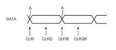
도 3a 내지 3d는 도 2에 도시된 위상 검출부(210)의 동작을 보여주는 도면이다. 상기 위상 검출부(210)는 상기 클럭 신호(CLK) 및 데이터(DATA)를 비교하여 상기 얼리 위상 감지 신호(ER) 및 상기 레이트 위상 감지 신호(LT)를 생성할 수 있다. 상기 위상 검출부(210)는 상기 클럭 신호(CLK)의 1주기 동안 상기 클럭 신호(CLK)의 0도, 90도, 180 및 270도에 해당하는 위상에서 상기 데이터(DATA)의 레벨을 캐치할 수 있다. 이를 위해, 상기 위상 검출부(210)는 상기 클럭 신호(CLK)를 분주한 분주 클럭 신호를 이용할 수 있고, 상기 분주 클럭 신호의 라이징 에지에서 상기 데이터(DATA)의 레벨을 캐치할 수 있다. 상기 분주 클럭 신호는 상기 위상 보간기(240)에서 생성될 수 있고, 상기 위상 검출부(210)에서 분주될 수도 있다. 도 3a 내지 도 3c에서, 상기 분주 클럭 신호(CLKI)는 상기 클럭 신호(CLK)와 동일한 위상을 가질 수 있고, 상기 분주 클럭 신호(CLKQ)는 상기 클럭 신호(CLK)에 비해 90도 지연된 위상을 가질 수 있으며, 상기 분주 클럭 신호(CLKIB)는 상기 클럭 신호(CLK)에 비해 180도 지연된 위상을 가질 수 있고, 상기 분주 클럭 신호(CLKQB)는 상기 클럭 신호(CLK)에 비해 270도 지연된 위상을 가질 수 있다.3A to 3D are diagrams showing the operation of the
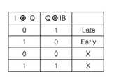
도 3a는 클럭 신호(CLK)의 위상 조절이 필요 없는 경우, 즉, 락킹 상태(Locking state)를 도시한다. 락킹 상태에서, 상기 분주 클럭 신호(CLKI, CLKIB)의 라이징 에지는 상기 데이터(DATA)의 천이 시점(A)에 위치될 수 있다. 상기 분주 클럭 신호(CLKQ, CLKQB)의 라이징 에지는 상기 데이터(DATA)의 유효 구간의 중앙 부분에 위치될 수 있다. 상기 위상 검출부(210)는 상기 분주 클럭 신호(CLKI, CLKQ, CLKIB, CLKQB)의 라이징 에지에서 캐치된 데이터(DATA)의 레벨을 연산하여 상기 얼리 위상 감지 신호(ER) 및 상기 레이트 위상 감지 신호(LT)를 생성할 수 있다. 상기 위상 검출부(210)는 상기 분주 클럭 신호(CLKI)에 의해 캐치된 데이터의 레벨과 상기 분주 클럭 신호(CLKQ)에 의해 캐치된 데이터의 레벨을 XOR 연산하고, 상기 분주 클럭 신호(CLKQ)에 의해 캐치된 데이터의 레벨과 상기 분주 클럭 신호(CLKIB)에 의해 캐치된 데이터의 레벨을 XOR 연산할 수 있다. 상기 위상 검출부(210)는 상기 XOR 연산 결과에 기초하여 상기 얼리 위상 감지 신호(ER) 및 상기 레이트 위상 감지 신호(LT)를 생성할 수 있다. 도 3b에 도시된 표와 같이, 상기 위상 검출부(210)는 상기 분주 클럭 신호(CLKI, CLKQ)에 의해 캐치된 데이터의 레벨(I, Q)이 동일하여 XOR 연산된 결과가 0이고 상기 분주 클럭 신호(CLKQ, CLKIB)에 의해 캐치된 데이터의 레벨(Q, IB)이 상이하여 XOR 연산된 결과가 1인 경우, 상기 클럭 신호(CLK)의 에지의 위상이 상기 데이터(DATA)의 천이 시점보다 늦다고 판단하고(Late), 상기 레이트 위상 감지 신호(LT)를 생성할 수 있다. 반대로, 상기 위상 검출부(210)는 상기 분주 클럭 신호(CLKI, CLKQ)에 의해 캐치된 데이터의 레벨(I, Q)이 상이하여 XOR 연산 결과가 1이고, 상기 분주 클럭 신호(CLKQ, CLKIB)에 의해 캐치된 데이터의 레벨(Q, IB)이 동일하여 XOR 연산 결과가 0인 경우, 상기 클럭 신호(CLK)의 에지의 위상이 상기 데이터(DATA)의 천이 시점보다 앞선다고 판단하고, 상기 얼리 위상 감지 신호(ER)를 생성할 수 있다. 상기 2가지 경우에 해당하지 않는 경우, 상기 위상 검출부(210)는 상기 얼리 위상 감지 신호(ER) 및 상기 레이트 위상 감지 신호(LT) 모두를 생성하지 않을 수 있다.FIG. 3A shows a case where the phase adjustment of the clock signal CLK is not required, that is, a locked state. In the locked state, the rising edge of the divided clock signals CLKI and CLKIB may be located at the transition point A of the data (DATA). The rising edge of the divided clock signals CLKQ and CLKQB may be located at the center of the valid period of the data DATA. The
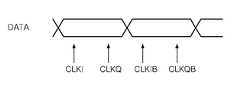
도 3c는 상기 클럭 신호(CLK)의 에지의 위상이 상기 데이터(DATA)의 천이 시점보다 늦은 경우를 보여준다. 상기 데이터(DATA)가 토글한다면, 상기 분주 클럭 신호(CLKI. CLKQ)에 의해 캐치된 데이터의 레벨(I, Q)은 동일하고, 상기 분주 클럭 신호(CLKQ, CLKIB)에 의해 캐치된 데이터의 레벨(Q, IB)은 상이할 것이다. 따라서, 도 3c의 경우 상기 위상 검출부(210)는 레이트 위상 감지 신호(LT)를 생성할 수 있다. 도 3d는 상기 클럭 신호(CLK)의 위상이 상기 데이터(DATA)의 천이 시점보다 빠른 경우를 보여준다. 상기 분주 클럭 신호(CLKI, CLKQ)에 의해 캐치된 데이터의 레벨(I, Q)은 상이하고, 상기 분주 클럭 신호(CLKQ, CLKIB)에 의해 캐치된 데이터의 레벨(Q, IB)은 동일할 것이다. 따라서, 도 3d의 경우 상기 위상 검출부(210)는 얼리 위상 감지 신호(ER)를 생성할 수 있다.3C shows a case where the phase of the edge of the clock signal CLK is later than the transition point of the data DATA. The level (I, Q) of the data caught by the divided clock signal CLKI.CLKQ is the same and the level of the data caught by the divided clock signals CLKQ and CLKIB (Q, IB) will be different. 3C, the
도 4는 도 2에 도시된 위상 정보 합산부(230)의 구성을 개략적으로 보여주는 블록도이다. 도 4에서, 상기 위상 정보 합산부(230)는 업 신호 합산기(410) 및 다운 신호 합산기(420)를 포함할 수 있다. 상기 업 신호 합산기(410)는 상기 필터링부(220)에서 출력되는 업 신호(UP), 상기 클럭 신호(CLK) 및 상기 제 2 클럭 신호(CLK/n)를 수신하여 상기 제 1 위상 제어신호(MAFUP<0:m>)를 생성할 수 있다. 상기 업 신호 합산기(410)는 상기 합산 시간 동안 입력되는 업 신호(UP)의 개수를 합산하여 출력할 수 있다. 상기 업 신호 합산기(410)는 상기 클럭 신호(CLK)의 주기마다 상기 업 신호(UP)를 수신할 수 있고, 상기 제 2 클럭 신호(CLK/n)의 주기마다 합산된 업 신호(UP)의 개수에 대응하는 정보를 상기 제 1 위상 제어 신호(MAFUP<0:m>)로서 출력할 수 있다. 상기 업 신호 합산기(410)는 상기 합산 시간 동안 합산된 상기 업 신호(UP)의 개수를 복수 비트의 이진 코드로 출력할 수 있다.FIG. 4 is a block diagram schematically showing the configuration of the phase
상기 다운 신호 합산기(420)는 상기 필터링부(220)에서 출력되는 다운 신호(DN), 상기 클럭 신호(CLK) 및 상기 제 2 클럭 신호(CLK/n)를 수신하여 상기 제 2 위상 제어 신호(MAFDN<0:m>)를 생성할 수 있다. 상기 다운 신호 합산기(420)는 상기 합산 시간 동안 입력되는 다운 신호(DN)의 개수를 합산하여 출력할 수 있다. 상기 다운 신호 합산기(420)는 상기 클럭 신호(CLK)의 주기마다 상기 다운 신호(DN)를 수신할 수 있고, 상기 제 2 클럭 신호(CLK/n)의 주기마다 합산된 다운 신호(DN)의 개수에 대응하는 정보를 상기 제 2 위상 제어 신호(MAFDN<0:m>)로서 출력할 수 있다. 상기 다운 신호 합산기(DN)는 상기 합산 시간 동안 합산된 상기 다운 신호(DN)의 개수를 복수 비트의 이진 코드로 출력할 수 있다.The down-
도 5는 도 4에 도시된 업 신호 합산기(410)의 구성을 보여주는 도면이다. 도 5에서, 상기 업 신호 합산기(410)는 XOR 게이트(501), AND 게이트(503), 제 1 내지 제 3 플립플롭(511, 513, 515)을 포함할 수 있다. 상기 XOR 게이트(501)는 상기 업 신호(UP)와 상기 제 1 플립플롭(511)의 출력을 수신하여 섬 신호(SUMUP)를 생성할 수 있다. 상기 AND 게이트(503)는 상기 업 신호(UP)와 상기 제 1 플립플롭(511)의 출력을 수신하여 캐리 신호(CARRYUP)를 생성할 수 있다. 상기 제 1 플립플롭(511)은 상기 섬 신호(SUMUP)와 상기 클럭 신호(CLK)를 수신하여 상기 지연 섬 신호(SUMUPD)를 생성할 수 있다. 상기 제 2 플립플롭(513)은 상기 섬 신호(SUMUP)와 상기 제 2 클럭 신호(CLK/4)를 수신하여 상기 제 1 위상 제어 신호의 최하위 비트(MAFUP<0>)를 생성할 수 있다. 상기 제 3 플립플롭(515)은 상기 캐리 신호(CARRYUP)와 상기 제 2 클럭 신호(CLK/4)를 수신하여 상기 제 1 위상 제어 신호의 최상위 비트(MAFUP<1>)를 생성할 수 있다. 도 5에서, n은 4이고, 상기 업 신호 합산기(410)는 상기 합산 시간 동안 2개의 업 신호(UP)를 합산할 수 있는 구성을 도시하였으나, 상기 업 신호 합산기(410)는 위와 같은 방식을 이용하여 더 많은 수의 업 신호(UP)를 합산할 수 있는 구성을 갖도록 수정되거나 다른 구성요소가 추가될 수 있을 것이다. 상기 다운 신호 합산기(420)는 업 신호(UP) 대신에 다운 신호(DN)를 수신하는 것에서 차이가 있을 뿐이고, 상기 업 신호 합산기(410)와 실질적으로 동일한 구성을 가질 수 있다.FIG. 5 is a diagram illustrating the configuration of the up-
도 6은 도 5에 도시된 업 신호 합산기(410)의 동작을 보여주는 타이밍도이다. 상기 합산 시간, 즉, 상기 제 2 클럭 신호(CLK/n)의 주기 동안 2개의 업 신호(UP)가 입력된다고 가정하자. 첫 번째 업 신호(UP(1))가 입력되면, 상기 XOR 게이트(501)는 하이 레벨의 섬 신호(SUMUP)를 출력하고, 상기 AND 게이트(503)는 로우 레벨의 캐리 신호(CARRYUP)를 출력할 수 있다. 상기 섬 신호(SUMUP)는 상기 제 1 플립플롭(511)에 의해 상기 클럭 신호(CLK)의 주기만큼 지연되어 상기 지연 섬 신호(SUMUPD)로 출력될 수 있다. 두 번째 업 신호(UP(2))가 입력되면, 상기 XOR 게이트(501)는 로우 레벨의 섬 신호(SUMUP)를 출력하고, 상기 AND 게이트(503)는 하이 레벨의 캐리 신호(CARRYUP)를 출력할 수 있다. 상기 제 2 플립플롭(513)은 상기 제 2 클럭 신호(CLK/n)에 응답하여 상기 로우 레벨의 섬 신호(SUMUP)를 상기 제 1 위상 제어 신호의 최하위 비트(MAFUP<0>)로 출력하고, 상기 제 3 플립플롭(515)은 상기 제 2 클럭 신호(CLK/n)에 응답하여 하이 레벨의 캐리 신호(CARRYUP)를 상기 제 1 위상 제어 신호의 최상위 비트(MAFUP<1>)로 출력할 수 있다. 따라서, 상기 제 1 위상 제어 신호(MAFUP<0:1>)는 1,0의 논리 값을 가질 수 있고, 상기 합산 시간 동안 상기 업 신호(UP)가 2회 생성되었다는 정보를 가질 수 있다.6 is a timing diagram showing the operation of the up-
상기 필터링부(220)는 상기 위상 검출부(210)로부터 출력되는 얼리 위상 감지 신호(ER)와 레이트 위상 감지 신호(LT)를 상기 클럭 주기(CLK)마다 수신하여 연산하므로, 상대적으로 짧은 주기로 위상 정보를 획득할 수 있다. 상기 위상 정보 합산부(230)는 상기 위상 검출부(210) 및 상기 필터링부(220)가 짧은 주기로 위상 정보를 획득하더라도, 상대적으로 긴 주기 동안 획득된 위상 정보를 합산할 수 있다. 상기 위상 보간기(240)는 상대적으로 긴 주기마다 합산된 위상 정보에 따라 업데이트될 수 있다. 따라서, 상기 클럭 데이터 리커버리 회로(2) 및 이를 이용하는 시스템(1)에서 소모되는 전력을 효율적으로 감소시킬 수 있다.Since the
본 발명이 속하는 기술분야의 당업자는 본 발명이 그 기술적 사상이나 필수적 특징을 변경하지 않고서 다른 구체적인 형태로 실시될 수 있으므로, 이상에서 기술한 실시예들은 모든 면에서 예시적인 것이며 한정적인 것이 아닌 것으로서 이해해야만 한다. 본 발명의 범위는 상기 상세한 설명보다는 후술하는 특허청구범위에 의하여 나타내어지며, 특허청구범위의 의미 및 범위 그리고 그 등가개념으로부터 도출되는 모든 변경 또는 변형된 형태가 본 발명의 범위에 포함되는 것으로 해석되어야 한다.It will be understood by those skilled in the art that various changes in form and details may be made therein without departing from the spirit and scope of the present invention as defined by the following claims and their equivalents. Only. The scope of the present invention is defined by the appended claims rather than the detailed description and all changes or modifications derived from the meaning and scope of the claims and their equivalents are to be construed as being included within the scope of the present invention do.
Claims (15)
Translated fromKorean상기 얼리 위상 감지 신호의 생성 횟수와 상기 레이트 위상 감지 신호의 생성 횟수에 따라 업 신호 및 다운 신호를 생성하는 필터링부;
상기 클럭 신호의 주기마다 상기 필터링부의 출력을 수신하고, 상기 클럭 신호의 주기의 n 배 (n은 2이상의 정수)에 해당하는 합산 시간 동안 상기 필터링부로부터 수신된 상기 업 신호 및 상기 다운 신호의 개수를 합산하여 제 1 및 제 2 위상 제어 신호를 생성하는 위상 정보 합산부; 및
상기 제 1 및 제 2 위상 제어 신호에 응답하여 상기 클럭 신호의 위상을 조절하는 위상 보간기를 포함하는 클럭 데이터 리커버리 회로.A phase detector for comparing the clock signal and data to generate an early phase sense signal and a rate phase sense signal;
A filtering unit for generating an up signal and a down signal according to the number of generation of the early phase sense signal and the number of generation of the rate phase sense signal;
And the number of the up signal and the down signal received from the filtering unit during a summation time corresponding to n times (n is an integer equal to or greater than 2) times the period of the clock signal, A phase information summation unit for generating first and second phase control signals; And
And a phase interpolator to adjust the phase of the clock signal in response to the first and second phase control signals.
상기 위상 검출부는 상기 클럭 신호의 분주 클럭 신호의 라이징 에지에서 상기 데이터의 레벨을 캐치하고, 캐치된 결과를 연산하여 상기 얼리 위상 감지 신호 및 상기 레이트 위상 감지 신호를 생성하는 클럭 데이터 리커버리 회로.The method according to claim 1,
Wherein the phase detector captures the level of the data at the rising edge of the clock signal of the clock signal and calculates the caught result to generate the early phase sense signal and the rate phase sense signal.
상기 필터링부는 상기 얼리 위상 감지 신호의 생성 횟수와 상기 레이트 위상 감지 신호의 생성 횟수의 차이가 소정 개수에 도달했을 때, 상기 업 신호 및 상기 다운 신호 중 하나를 생성하는 클럭 데이터 리커버리 회로.The method according to claim 1,
Wherein the filtering unit generates one of the up signal and the down signal when a difference between the number of times of generation of the early phase sense signal and the number of times of generation of the rate phase sense signal reaches a predetermined number.
상기 필터링부는 무빙 에버리지 필터인 클럭 데이터 리커버리 회로.The method according to claim 1,
Wherein the filtering unit is an moving average filter.
상기 위상 정보 합산부는 상기 합산 시간 동안 상기 필터링부로부터 출력된 상기 업 신호의 개수를 합산하여 상기 제 1 위상 제어 신호를 출력하는 업 신호 합산기; 및
상기 합산 시간 동안 상기 필터링부로부터 출력된 상기 다운 신호의 개수를 합산하여 상기 제 2 위상 제어 신호를 출력하는 다운 신호 합산기를 포함하는 클럭 데이터 리커버리 회로.The method according to claim 1,
Wherein the phase information summation unit comprises: an up-signal adder for summing up the number of up signals output from the filtering unit during the summation time and outputting the first phase control signal; And
And a down signal adder for summing the number of the down signals output from the filtering unit during the summing time to output the second phase control signal.
상기 업 신호 합산기는 상기 클럭 신호의 주기마다 상기 업 신호의 출력 여부를 감지하고, 상기 합산 시간 동안 합산된 상기 업 신호의 개수를 복수 비트의 이진 코드로 출력하는 클럭 데이터 리커버리 회로.6. The method of claim 5,
Wherein the up signal adder detects whether the up signal is output for each cycle of the clock signal and outputs the number of the up signals summed during the sum time as a binary code of a plurality of bits.
상기 다운 신호 합산기는 상기 클럭 신호의 주기마다 상기 다운 신호의 출력 여부를 감지하고, 상기 합산 시간 동안 합산된 상기 다운 신호의 개수를 복수 비트의 이진 코드로 출력하는 클럭 데이터 리커버리 회로.6. The method of claim 5,
Wherein the down signal adder detects whether the down signal is output every period of the clock signal and outputs the number of the down signals added during the sum time as a binary code of a plurality of bits.
상기 얼리 위상 감지 신호의 생성 횟수와 상기 레이트 위상 감지 신호의 생성 횟수에 따라 업 신호 및 다운 신호를 생성하는 필터링부;
상기 제 1 클럭 신호에 동기하여 상기 업 신호 및 상기 다운 신호의 생성 횟수를 합산하고, 합산된 결과를 제 2 클럭 신호에 동기하여 제 1 및 제 2 위상 제어 신호로서 출력하는 위상 정보 합산부; 및
상기 제 2 클럭 신호에 동기하여 업데이트될 때 상기 제 1 및 제 2 위상 제어 신호에 기초하여 상기 제 1 클럭 신호의 위상을 보정하는 위상 보간기를 포함하는 클럭 데이터 리커버리 회로.A phase detector for comparing the data with the first clock signal to generate an early phase sense signal and a rate phase sense signal;
A filtering unit for generating an up signal and a down signal according to the number of generation of the early phase sense signal and the number of generation of the rate phase sense signal;
A phase information summation unit for summing up the number of times of generation of the up signal and the down signal in synchronization with the first clock signal and for outputting the summed result as first and second phase control signals in synchronization with the second clock signal; And
And a phase interpolator for correcting the phase of the first clock signal based on the first and second phase control signals when updated in synchronization with the second clock signal.
상기 제 2 클럭 신호의 주기는 상기 제 1 클럭 신호의 주기의 n 배(n은 2 이상의 정수)인 클럭 데이터 리커버리 회로.9. The method of claim 8,
Wherein the period of the second clock signal is n times (n is an integer of 2 or more) times the period of the first clock signal.
상기 위상 검출부는 상기 제 1 클럭 신호의 분주 클럭 신호의 라이징 에지에서 상기 데이터의 레벨을 캐치하고, 캐치된 결과를 연산하여 상기 얼리 위상 감지 신호 및 상기 레이트 위상 감지 신호를 생성하는 클럭 데이터 리커버리 회로.9. The method of claim 8,
Wherein the phase detector captures the level of the data at the rising edge of the divided clock signal of the first clock signal and calculates the caught result to generate the early phase sense signal and the rate phase sense signal.
상기 필터링부는 상기 얼리 위상 감지 신호의 생성 횟수와 상기 레이트 위상 감지 신호의 생성 횟수의 차이가 소정 개수에 도달했을 때, 상기 업 신호 및 상기 다운 신호 중 하나를 생성하는 클럭 데이터 리커버리 회로.9. The method of claim 8,
Wherein the filtering unit generates one of the up signal and the down signal when a difference between the number of times of generation of the early phase sense signal and the number of times of generation of the rate phase sense signal reaches a predetermined number.
상기 필터링부는 무빙 에버리지 필터인 클럭 데이터 리커버리 회로.9. The method of claim 8,
Wherein the filtering unit is an moving average filter.
상기 위상 정보 합산부는 상기 제 2 클럭 신호의 주기에 대응하는 시간 동안 상기 필터링부로부터 출력된 상기 업 신호의 개수를 합산하여 출력하는 업 신호 합산기; 및
상기 제 2 클럭 신호의 주기에 대응하는 시간 동안 상기 필터링부로부터 출력된 상기 다운 신호의 개수를 합산하여 출력하는 다운 신호 합산기를 포함하는 클럭 데이터 리커버리 회로.9. The method of claim 8,
Wherein the phase information summation unit comprises: an up-signal adder for summing up the number of the up signals output from the filtering unit for a time corresponding to the period of the second clock signal; And
And a down signal adder for summing up the number of the down signals output from the filtering unit for a time corresponding to the period of the second clock signal and outputting the sum.
상기 업 신호 합산기는 상기 제 1 클럭 신호의 주기마다 상기 업 신호의 출력 여부를 감지하고, 상기 제 2 클럭 신호의 주기에 대응하는 동안 합산된 상기 업 신호의 개수를 복수 비트의 이진 코드로 출력하는 클럭 데이터 리커버리 회로.14. The method of claim 13,
The up signal adder senses whether the up signal is output every period of the first clock signal and outputs the number of the up signals added during the period of the second clock signal as a binary code of a plurality of bits Clock data recovery circuit.
상기 다운 신호 합산기는 상기 제 1 클럭 신호의 주기마다 상기 다운 신호의 출력 여부를 감지하고, 상기 제 2 클럭 신호의 주기에 대응하는 시간 동안 합산된 상기 다운 신호의 개수를 복수 비트의 이진 코드로 출력하는 클럭 데이터 리커버리 회로.14. The method of claim 13,
Wherein the down signal adder detects whether the down signal is output for each period of the first clock signal and outputs the number of the down signals added during a period corresponding to the period of the second clock signal in a binary code of a plurality of bits Clock data recovery circuit.
Priority Applications (3)
| Application Number | Priority Date | Filing Date | Title |
|---|---|---|---|
| KR1020140174449AKR20160069093A (en) | 2014-12-05 | 2014-12-05 | Clock and data recovery circuit and system using the same |
| US14/666,537US9602272B2 (en) | 2014-12-05 | 2015-03-24 | Clock and data recovery circuit and system using the same |
| CN201510558134.XACN105680831B (en) | 2014-12-05 | 2015-09-02 | Clock and data recovery circuits and systems using the same |
Applications Claiming Priority (1)
| Application Number | Priority Date | Filing Date | Title |
|---|---|---|---|
| KR1020140174449AKR20160069093A (en) | 2014-12-05 | 2014-12-05 | Clock and data recovery circuit and system using the same |
Publications (1)
| Publication Number | Publication Date |
|---|---|
| KR20160069093Atrue KR20160069093A (en) | 2016-06-16 |
Family
ID=56095304
Family Applications (1)
| Application Number | Title | Priority Date | Filing Date |
|---|---|---|---|
| KR1020140174449AWithdrawnKR20160069093A (en) | 2014-12-05 | 2014-12-05 | Clock and data recovery circuit and system using the same |
Country Status (3)
| Country | Link |
|---|---|
| US (1) | US9602272B2 (en) |
| KR (1) | KR20160069093A (en) |
| CN (1) | CN105680831B (en) |
Families Citing this family (2)
| Publication number | Priority date | Publication date | Assignee | Title |
|---|---|---|---|---|
| KR102671076B1 (en)* | 2017-02-09 | 2024-05-30 | 에스케이하이닉스 주식회사 | Internal clock generation circuit |
| US11489657B1 (en)* | 2021-10-20 | 2022-11-01 | Diodes Incorporated | Bit-level mode retimer |
Family Cites Families (11)
| Publication number | Priority date | Publication date | Assignee | Title |
|---|---|---|---|---|
| US7003066B1 (en)* | 2001-12-03 | 2006-02-21 | Lattice Semiconductor Corporation | Digital phase locked loop with phase selector having minimized number of phase interpolators |
| JP3660638B2 (en)* | 2002-03-27 | 2005-06-15 | 株式会社東芝 | Clock extraction circuit |
| JP4741003B2 (en)* | 2006-07-28 | 2011-08-03 | パナソニック株式会社 | Phase comparator, phase comparator, and clock data recovery system |
| JP5135009B2 (en)* | 2008-03-13 | 2013-01-30 | 株式会社日立製作所 | Clock data recovery circuit |
| CN103053140B (en)* | 2010-08-03 | 2015-01-28 | 松下电器产业株式会社 | Adaptive receiver system and adaptive transceiver system |
| US8537955B1 (en)* | 2010-09-28 | 2013-09-17 | Agilent Technologies, Inc. | System and method for compensating for loop filter delay |
| KR101893185B1 (en)* | 2012-02-20 | 2018-08-29 | 에스케이하이닉스 주식회사 | Data output timing control circuit of semiconductor apparatus |
| US8938043B2 (en) | 2012-03-29 | 2015-01-20 | Terasquare Co., Ltd. | Adaptive optimum CDR bandwidth estimation by using a kalman gain extractor |
| CN102751984B (en)* | 2012-06-29 | 2015-04-22 | 无锡思泰迪半导体有限公司 | High-speed clock data recovery system realization method and structure using same |
| US9184907B2 (en)* | 2012-12-28 | 2015-11-10 | Nvidia Corporation | Flexible threshold counter for clock-and-data recovery |
| CN203708218U (en)* | 2014-01-07 | 2014-07-09 | 英特格灵芯片(天津)有限公司 | Clock data recovery circuit |
- 2014
- 2014-12-05KRKR1020140174449Apatent/KR20160069093A/ennot_activeWithdrawn
- 2015
- 2015-03-24USUS14/666,537patent/US9602272B2/enactiveActive
- 2015-09-02CNCN201510558134.XApatent/CN105680831B/enactiveActive
Also Published As
| Publication number | Publication date |
|---|---|
| US20160164667A1 (en) | 2016-06-09 |
| CN105680831A (en) | 2016-06-15 |
| US9602272B2 (en) | 2017-03-21 |
| CN105680831B (en) | 2020-08-14 |
Similar Documents
| Publication | Publication Date | Title |
|---|---|---|
| US10965290B2 (en) | Phase rotation circuit for eye scope measurements | |
| US10103870B2 (en) | CDR circuit and reception circuit | |
| US9577815B1 (en) | Clock data alignment system for vector signaling code communications link | |
| US9520883B2 (en) | Frequency detection circuit and reception circuit | |
| CN111512369B (en) | Clock data recovery device and method for multi-channel data receiver | |
| KR102577232B1 (en) | Hybrid clock data recovery circuit and receiver | |
| CN113497701B (en) | Phase detector command propagation between channels in MCM USR SERDES | |
| KR20210139388A (en) | Multiphase clock duty cycle and skew measurement and correction | |
| US8149980B2 (en) | System and method for implementing a phase detector to support a data transmission procedure | |
| US10615956B2 (en) | Clock and data recovery device and phase detection method | |
| WO2011004580A1 (en) | Clock data recovery circuit | |
| US9722590B1 (en) | Skew adjustment circuit, semiconductor device, and skew calibration method | |
| CN103490775A (en) | Clock data recovery controller based on dual-loop structure | |
| KR101470599B1 (en) | Apparatus of receiving data transmitted by using recovered clock | |
| KR20160069093A (en) | Clock and data recovery circuit and system using the same | |
| US10374615B2 (en) | Transmission circuit and integrated circuit | |
| JP2015100017A (en) | Phase comparison circuit and clock data recovery circuit | |
| US9350527B1 (en) | Reception unit and receiving method | |
| US7664215B2 (en) | Signal alignment based on data signal | |
| JP4387410B2 (en) | Receiver for cyclically encoded signals | |
| CN108011620B (en) | Fast clock recovery circuit based on FPGA | |
| KR101030600B1 (en) | Serial I / O Interface Using Phase Modulation Technology | |
| KR20160069092A (en) | Clock and data recovery circuit and system using the same | |
| Song et al. | Clock-and data-recovery circuit with independently controlled eye-tracking loop for high-speed graphic DRAMs | |
| KR0157923B1 (en) | Menchester decoder |
Legal Events
| Date | Code | Title | Description |
|---|---|---|---|
| PA0109 | Patent application | Patent event code:PA01091R01D Comment text:Patent Application Patent event date:20141205 | |
| PG1501 | Laying open of application | ||
| PC1203 | Withdrawal of no request for examination | ||
| WITN | Application deemed withdrawn, e.g. because no request for examination was filed or no examination fee was paid |