KR20160061316A - Voltage controlled nano-magnetic random number generator - Google Patents
Voltage controlled nano-magnetic random number generatorDownload PDFInfo
- Publication number
- KR20160061316A KR20160061316AKR1020167004713AKR20167004713AKR20160061316AKR 20160061316 AKR20160061316 AKR 20160061316AKR 1020167004713 AKR1020167004713 AKR 1020167004713AKR 20167004713 AKR20167004713 AKR 20167004713AKR 20160061316 AKR20160061316 AKR 20160061316A
- Authority
- KR
- South Korea
- Prior art keywords
- ferromagnetic layer
- mtj
- current
- bias voltage
- free ferromagnetic
- Prior art date
- Legal status (The legal status is an assumption and is not a legal conclusion. Google has not performed a legal analysis and makes no representation as to the accuracy of the status listed.)
- Ceased
Links
Images


Classifications
- H01L43/02—
- H—ELECTRICITY
- H10—SEMICONDUCTOR DEVICES; ELECTRIC SOLID-STATE DEVICES NOT OTHERWISE PROVIDED FOR
- H10N—ELECTRIC SOLID-STATE DEVICES NOT OTHERWISE PROVIDED FOR
- H10N50/00—Galvanomagnetic devices
- H10N50/10—Magnetoresistive devices
- B—PERFORMING OPERATIONS; TRANSPORTING
- B82—NANOTECHNOLOGY
- B82Y—SPECIFIC USES OR APPLICATIONS OF NANOSTRUCTURES; MEASUREMENT OR ANALYSIS OF NANOSTRUCTURES; MANUFACTURE OR TREATMENT OF NANOSTRUCTURES
- B82Y25/00—Nanomagnetism, e.g. magnetoimpedance, anisotropic magnetoresistance, giant magnetoresistance or tunneling magnetoresistance
- G—PHYSICS
- G06—COMPUTING OR CALCULATING; COUNTING
- G06F—ELECTRIC DIGITAL DATA PROCESSING
- G06F1/00—Details not covered by groups G06F3/00 - G06F13/00 and G06F21/00
- G06F1/16—Constructional details or arrangements
- G06F1/1613—Constructional details or arrangements for portable computers
- G—PHYSICS
- G06—COMPUTING OR CALCULATING; COUNTING
- G06F—ELECTRIC DIGITAL DATA PROCESSING
- G06F17/00—Digital computing or data processing equipment or methods, specially adapted for specific functions
- G—PHYSICS
- G06—COMPUTING OR CALCULATING; COUNTING
- G06F—ELECTRIC DIGITAL DATA PROCESSING
- G06F3/00—Input arrangements for transferring data to be processed into a form capable of being handled by the computer; Output arrangements for transferring data from processing unit to output unit, e.g. interface arrangements
- G06F3/01—Input arrangements or combined input and output arrangements for interaction between user and computer
- G06F3/03—Arrangements for converting the position or the displacement of a member into a coded form
- G06F3/041—Digitisers, e.g. for touch screens or touch pads, characterised by the transducing means
- G—PHYSICS
- G06—COMPUTING OR CALCULATING; COUNTING
- G06F—ELECTRIC DIGITAL DATA PROCESSING
- G06F7/00—Methods or arrangements for processing data by operating upon the order or content of the data handled
- G06F7/58—Random or pseudo-random number generators
- G06F7/588—Random number generators, i.e. based on natural stochastic processes
- G—PHYSICS
- G11—INFORMATION STORAGE
- G11C—STATIC STORES
- G11C11/00—Digital stores characterised by the use of particular electric or magnetic storage elements; Storage elements therefor
- G11C11/02—Digital stores characterised by the use of particular electric or magnetic storage elements; Storage elements therefor using magnetic elements
- G11C11/16—Digital stores characterised by the use of particular electric or magnetic storage elements; Storage elements therefor using magnetic elements using elements in which the storage effect is based on magnetic spin effect
- H—ELECTRICITY
- H01—ELECTRIC ELEMENTS
- H01F—MAGNETS; INDUCTANCES; TRANSFORMERS; SELECTION OF MATERIALS FOR THEIR MAGNETIC PROPERTIES
- H01F10/00—Thin magnetic films, e.g. of one-domain structure
- H01F10/32—Spin-exchange-coupled multilayers, e.g. nanostructured superlattices
- H01F10/324—Exchange coupling of magnetic film pairs via a very thin non-magnetic spacer, e.g. by exchange with conduction electrons of the spacer
- H01F10/3254—Exchange coupling of magnetic film pairs via a very thin non-magnetic spacer, e.g. by exchange with conduction electrons of the spacer the spacer being semiconducting or insulating, e.g. for spin tunnel junction [STJ]
- H—ELECTRICITY
- H01—ELECTRIC ELEMENTS
- H01F—MAGNETS; INDUCTANCES; TRANSFORMERS; SELECTION OF MATERIALS FOR THEIR MAGNETIC PROPERTIES
- H01F10/00—Thin magnetic films, e.g. of one-domain structure
- H01F10/32—Spin-exchange-coupled multilayers, e.g. nanostructured superlattices
- H01F10/324—Exchange coupling of magnetic film pairs via a very thin non-magnetic spacer, e.g. by exchange with conduction electrons of the spacer
- H01F10/3268—Exchange coupling of magnetic film pairs via a very thin non-magnetic spacer, e.g. by exchange with conduction electrons of the spacer the exchange coupling being asymmetric, e.g. by use of additional pinning, by using antiferromagnetic or ferromagnetic coupling interface, i.e. so-called spin-valve [SV] structure, e.g. NiFe/Cu/NiFe/FeMn
- H01F10/3272—Exchange coupling of magnetic film pairs via a very thin non-magnetic spacer, e.g. by exchange with conduction electrons of the spacer the exchange coupling being asymmetric, e.g. by use of additional pinning, by using antiferromagnetic or ferromagnetic coupling interface, i.e. so-called spin-valve [SV] structure, e.g. NiFe/Cu/NiFe/FeMn by use of anti-parallel coupled [APC] ferromagnetic layers, e.g. artificial ferrimagnets [AFI], artificial [AAF] or synthetic [SAF] anti-ferromagnets
- H01L43/08—
- H01L43/10—
- H—ELECTRICITY
- H10—SEMICONDUCTOR DEVICES; ELECTRIC SOLID-STATE DEVICES NOT OTHERWISE PROVIDED FOR
- H10B—ELECTRONIC MEMORY DEVICES
- H10B61/00—Magnetic memory devices, e.g. magnetoresistive RAM [MRAM] devices
- H—ELECTRICITY
- H10—SEMICONDUCTOR DEVICES; ELECTRIC SOLID-STATE DEVICES NOT OTHERWISE PROVIDED FOR
- H10N—ELECTRIC SOLID-STATE DEVICES NOT OTHERWISE PROVIDED FOR
- H10N50/00—Galvanomagnetic devices
- H10N50/01—Manufacture or treatment
- H—ELECTRICITY
- H10—SEMICONDUCTOR DEVICES; ELECTRIC SOLID-STATE DEVICES NOT OTHERWISE PROVIDED FOR
- H10N—ELECTRIC SOLID-STATE DEVICES NOT OTHERWISE PROVIDED FOR
- H10N50/00—Galvanomagnetic devices
- H10N50/80—Constructional details
- H—ELECTRICITY
- H10—SEMICONDUCTOR DEVICES; ELECTRIC SOLID-STATE DEVICES NOT OTHERWISE PROVIDED FOR
- H10N—ELECTRIC SOLID-STATE DEVICES NOT OTHERWISE PROVIDED FOR
- H10N50/00—Galvanomagnetic devices
- H10N50/80—Constructional details
- H10N50/85—Materials of the active region
Landscapes
- Engineering & Computer Science (AREA)
- Theoretical Computer Science (AREA)
- Physics & Mathematics (AREA)
- General Physics & Mathematics (AREA)
- General Engineering & Computer Science (AREA)
- Chemical & Material Sciences (AREA)
- Crystallography & Structural Chemistry (AREA)
- Power Engineering (AREA)
- Pure & Applied Mathematics (AREA)
- Human Computer Interaction (AREA)
- Computational Mathematics (AREA)
- Mathematical Analysis (AREA)
- Mathematical Optimization (AREA)
- Computer Hardware Design (AREA)
- Nanotechnology (AREA)
- Databases & Information Systems (AREA)
- Data Mining & Analysis (AREA)
- Mathematical Physics (AREA)
- Software Systems (AREA)
- Manufacturing & Machinery (AREA)
- Hall/Mr Elements (AREA)
- Mram Or Spin Memory Techniques (AREA)
- Measuring Magnetic Variables (AREA)
Abstract
Translated fromKoreanDescription
Translated fromKorean온 칩 마이크로-스케일의 내장된 난수 발생기(random number generator)(RNG)들은 소비자와 기업 애플리케이션을 위한 광범위한 보안 특징들을 가능하게 할 수 있다. 그러나, 의사 난수 발생기들을 이끄는 것은 네트워크화된 소스(예를 들어, 미국 국립 표준 기술 연구소(NIST))에 기반하거나 이로부터 공급되는 소프트웨어이다. 소프트웨어 기반의 난수 발생기들은, 난수 발생기를 구동하기 위한 전력 및 칩 면적이 증가되는 것을 겪게 된다. RNG를 위한 표준화된 알고리즘들은 또한 보안 위협에 취약하다. 소프트웨어 알고리즘들은 알려진 무작위 테스트에 의해 측정되는 바와 같이 근사 난수 시퀀스이지만 제한된 품질의 난수 시퀀스를 생성할 수 있다.On-chip micro-scale embedded random number generators (RNGs) can enable a wide range of security features for consumer and enterprise applications. However, leading pseudorandom numbers generators is software based on or supplied from a networked source (e.g., the National Institute of Standards and Technology (NIST)). Software-based random number generators suffer from increased power and chip area for driving the random number generator. Standardized algorithms for RNGs are also vulnerable to security threats. Software algorithms can generate a random number sequence of limited quality but an approximate random number sequence as measured by known random tests.
기존 MTJ(magnetic tunnel junction) 기반의 난수 발생기들은 몇가지 단점들을 겪게 된다. 예를 들어, 알려진 MTJ 기반의 RNG들은 통신 암호화를 위해 가장 일반적으로 사용되는 프로세스들 중 하나인, 가우시안 분포 잡음을 생성할 수 없다. 알려진 MTJ 기반의 RNG들의 다른 단점은 변수 평균과 분산이 동적으로 변경될 수 있도록 난수 생성의 프로세스를 제어하기 위한 능력의 부재이다.Existing MTJ-based random number generators suffer from several disadvantages. For example, known MTJ-based RNGs can not generate Gaussian distributed noise, which is one of the most commonly used processes for communication encryption. Another disadvantage of known MTJ-based RNGs is the absence of the ability to control the process of generating random numbers such that the variable mean and variance can be changed dynamically.
본 개시 내용의 실시예들은 이하에 주어진 상세한 설명으로부터 및 본 개시 내용의 다양한 실시예들의 첨부 도면들로부터 보다 충분히 이해될 것이지만, 이들은 본 개시 내용을 특정 실시예들로 제한하는 것이 아니라 단지 설명 및 이해를 목적으로 취해져야 한다.
도 1a는 MTJ 기반의 RNG를 예시한다.
도 1b는 MTJ로부터 감지된 랜덤 전류와, 정규 잡음 분포를 나타내는 플롯을 예시한다.
도 2는 본 개시 내용의 일 실시예에 따라, 비공선적(non-collinear) MTJ 디바이스를 예시한다.
도 3은 본 개시 내용의 일 실시예에 따라, 비공선적 MTJ 디바이스의 평면도를 예시한다.
도 4a는 본 개시 내용의 일 실시예에 따라, 비공선적 MTJ 디바이스를 위한 자기 배리어(magnetic barrier)에 대한 자석 각도(magnet angle)의 분산을 나타내는 플롯을 예시한다.
도 4b는 본 개시 내용의 일 실시예에 따라, 비공선적 MTJ 디바이스를 위한 인가 전압에 대한 자기 배리어의 분산을 예시한다.
도 5a는 본 개시 내용의 일 실시예에 따라, 비공선적 MTJ 디바이스를 위한 잡음 전류 확률 밀도를 나타내는 플롯을 예시한다.
도 5b는 본 개시 내용의 일 실시예에 따라, 비공선적 MTJ 디바이스를 위한 누적된 확률 대 감지된 전류를 나타내는 플롯을 예시한다.
도 6의 (a) 및 (b)는 본 개시 내용의 일 실시예에 따라, 비공선적 MTJ 디바이스를 위한 인가 전압과 함께 자기 배리어를 변경하는 것에 의한 자기 잡음의 제어를 나타내는 플롯들을 예시한다.
도 7a 및 도 7b는 본 개시 내용의 일 실시예에 따라, 비공선적 MTJ에 고전압을 인가하는 것에 의한 비공선적 MTJ의 재설정 상태를 나타내는 플롯들을 예시한다.
도 8은 본 개시 내용의 일 실시예에 따라, 비공선적 MTJ에 의해 생성되는 전류의 전력 스펙트럼 밀도를 나타내는 플롯을 예시한다.
도 9는 본 개시 내용의 일 실시예에 따라, 랜덤 아날로그/디지털 신호를 생성하기 위한 및 비공선적 MTJ에 바이어스 전압을 인가하기 위한 회로이다.
도 10은 본 개시 내용의 일 실시예에 따라, 비공선적 MTJ 디바이스를 형성하는 방법의 흐름도이다.
도 11은 본 개시 내용의 일 실시예에 따른, 비공선적 MTJ를 갖는 난수 발생기를 갖는 스마트 디바이스 또는 컴퓨터 시스템 또는 SoC(system-on-chip)이다.BRIEF DESCRIPTION OF THE DRAWINGS Embodiments of the present disclosure will be understood more fully from the detailed description given hereinafter and from the accompanying drawings of various embodiments of the present disclosure, but they are not intended to limit the present disclosure to specific embodiments, To be taken for the purpose of.
1A illustrates an MTJ-based RNG.
Figure IB illustrates a plot showing the random current sensed from the MTJ and the normal noise distribution.
Figure 2 illustrates a non-collinear MTJ device, according to one embodiment of the present disclosure.
Figure 3 illustrates a top view of a non-paced MTJ device, in accordance with one embodiment of the present disclosure.
4A illustrates a plot showing the variance of a magnet angle to a magnetic barrier for a non-paced MTJ device, in accordance with one embodiment of the present disclosure.
4B illustrates dispersion of magnetic barriers for an applied voltage for a non-paced MTJ device, in accordance with one embodiment of the present disclosure.
5A illustrates a plot illustrating the noise current probability density for a non-piconet MTJ device, in accordance with one embodiment of the present disclosure.
FIG. 5B illustrates a plot representing cumulative probability versus sensed current for a non-reserved MTJ device, in accordance with one embodiment of the present disclosure.
Figures 6 (a) and 6 (b) illustrate plots illustrating control of magnetic noise by changing magnetic barriers with applied voltage for a non-paced MTJ device, in accordance with one embodiment of the present disclosure.
Figures 7A and 7B illustrate plots illustrating the reset state of a non-piconet MTJ by applying a high voltage to a non-piconet MTJ, in accordance with one embodiment of the present disclosure.
Figure 8 illustrates a plot showing the power spectral density of the current generated by the non-paced MTJ, in accordance with one embodiment of the present disclosure.
Figure 9 is a circuit for generating a random analog / digital signal and for applying a bias voltage to a non-paced MTJ, in accordance with one embodiment of the present disclosure.
10 is a flow diagram of a method for forming a non-piconet MTJ device, in accordance with one embodiment of the present disclosure.
FIG. 11 is a smart device or computer system or system-on-chip (SoC) with a random number generator with non-piconet MTJ, in accordance with one embodiment of the present disclosure.
실시예들은 전압 종속형 자기 배리어들을 갖는 비공선적(예를 들어, 직교의) 적층된 평면내(in-plane) MTJ(Magnetic Tunnel Junction) 디바이스를 제어가능한 난수 발생기로서 설명한다. 일 실시예에서, 난수 발생기는 종래 MTJ 디바이스들에 의한 잡음의 비 종-형상(bell-shaped)의 분포에 비해 종-형상의 정규 가우시안 분포를 제공한다. 일 실시예에서, MTJ 자유 및 고정 강자성층들은 MTJ 감지 전류의 정규 분포를 생성하기 위해 서로에 대해 비공선적 위치에 위치된다. 일 실시예에서, 생성된 MTJ 전류의 분산의 제어를 가능하게 하기 위해 MTJ 자유 강자성층의 자기 배리어를 제어하기 위한 바이어스 전압을 생성하는 회로가 제공된다. 일 실시예에서, 난수 발생기의 클린 리셋(clean reset)을 가능하게 하기 위해 MTJ의 자기 배리어를 낮추기 위한 바이어스 전압을 생성하는 회로가 제공된다.Embodiments describe a non-piconet (e.g., quadrature) stacked in-plane MTJ (Magnetic Tunnel Junction) device with voltage dependent magnetic barriers as a controllable random number generator. In one embodiment, the random number generator provides a longitudinal-shaped normal Gaussian distribution relative to a bell-shaped distribution of noise by conventional MTJ devices. In one embodiment, the MTJ free and fixed ferromagnetic layers are positioned in non-conductive positions relative to each other to produce a normal distribution of the MTJ sensing current. In one embodiment, a circuit is provided for generating a bias voltage for controlling the magnetic barrier of the MTJ free ferromagnetic layer to enable control of the dispersion of the generated MTJ current. In one embodiment, a circuit is provided for generating a bias voltage to lower the magnetic barrier of the MTJ to enable a clean reset of the random number generator.
다음의 설명에서, 본 개시 내용의 실시예들의 보다 철저한 설명을 제공하기 위해서 복수의 상세 사항이 논의된다. 그러나, 통상의 기술자에게는 본 개시 내용의 실시예들이 특정 상세 사항들 없이도 실시될 수 있다는 점이 명백할 것이다. 다른 경우에, 본 개시 내용의 실시예들을 모호하게 하는 것을 회피하기 위해서 잘 알려진 구조들 및 디바이스들은 상세하게가 아니라 블록도 형태로 도시된다.In the following description, numerous details are set forth in order to provide a more thorough description of embodiments of the present disclosure. However, it will be apparent to one of ordinary skill in the art that the embodiments of the present disclosure may be practiced without specific details. In other instances, well-known structures and devices are shown in block diagram form, rather than in detail, in order to avoid obscuring the embodiments of the present disclosure.
실시예들의 대응하는 도면들에서, 신호들은 라인들로 표현된다는 점에 유의한다. 일부 라인들은 더 많은 구성 신호 경로들을 표시하기 위해서 더 두꺼울 수 있고/있거나, 주요 정보 흐름 방향을 표시하기 위해서 하나 이상의 단부에서 화살표들을 가질 수 있다. 이러한 표시들은 제한하는 것으로 의도되지는 않는다. 오히려, 라인들은 회로 또는 논리 유닛의 보다 용이한 이해를 가능하게 하기 위해서 하나 이상의 예시적 실시예와 관련하여 사용된다. 설계 니즈 또는 선호도에 의해 결정된 바와 같은 임의의 표현된 신호는 임의의 적합한 유형의 신호 스킴으로 구현될 수 있고, 어느 방향으로도 이동할 수 있는 하나 이상의 신호를 실제로 포함할 수 있다.It should be noted that, in the corresponding figures of the embodiments, the signals are represented by lines. Some lines may be thicker to indicate more constituent signal paths and / or may have arrows at one or more ends to indicate a major information flow direction. These indications are not intended to be limiting. Rather, the lines are used in conjunction with one or more illustrative embodiments to enable a better understanding of the circuit or logic unit. Any expressed signal, as determined by design needs or preferences, may be implemented with any suitable type of signal scheme and may actually include one or more signals that are movable in either direction.
명세서 전체를 통해, 및 청구항들에서, 용어 "접속된"은, 어떠한 중간 디바이스도 없이, 접속되는 물체들 간의 직접적인 전기 접속을 의미한다. 용어 "결합된"은, 접속되는 물체들 간의 직접적인 전기 접속 또는 하나 이상의 수동 또는 능동 중간 디바이스들을 통한 간접 접속을 의미한다. 용어 "회로"는, 원하는 기능을 제공하기 위해 서로 협력하도록 배열된 하나 이상의 수동 및/또는 능동 컴포넌트를 의미한다. 용어 "신호"는 적어도 하나의 전류 신호, 전압 신호, 또는 데이터/클록 신호를 의미한다. 단수 표현("a", "an" 및 "the")의 의미는 복수 참조를 포함한다. "에서(in)"의 의미는 "에서(in)" 및 "상에(on)"를 포함한다.Throughout the specification, and in the claims, the term "connected" means a direct electrical connection between connected objects, without any intermediate device. The term "coupled" means a direct electrical connection between connected objects or an indirect connection via one or more passive or active intermediate devices. The term "circuit " means one or more passive and / or active components arranged to cooperate with each other to provide a desired function. The term "signal" means at least one current signal, voltage signal, or data / clock signal. The meaning of the singular expressions ("a", "an", and "the") includes multiple references. The meaning of " in "includes " in" and "on."
용어 "스케일링"이란 일반적으로 한 프로세스 기술로부터 또 다른 프로세스 기술로 설계(배선도 및 레이아웃)를 변환하는 것을 말한다. 용어 "스케일링"이란 또한, 레이아웃과 디바이스를 동일한 기술 노드 내에서 축소(downsize)하는 것을 말한다. 용어 "스케일링"이란 또한, 신호 주파수를, 또 다른 파라미터, 예를 들어 전원 레벨에 관하여 조절하는 것(예를 들어, 늦추는 것)을 말할 수도 있다. "실질적으로(substantially)", "근접한(close)", "대략(approximately)", "근처의(near)" 및 "약(about)"이라는 용어들은 일반적으로 타깃 값의 ±20% 내에 있는 것을 말한다.The term "scaling" generally refers to the conversion of a design (schematic and layout) from one process technology to another. The term "scaling" also refers to downsizing the layout and device within the same technology node. The term "scaling" may also refer to adjusting (e.g., slowing down) the signal frequency with respect to another parameter, e.g., a power level. The terms "substantially", "close", "approximately", "near", and "about" generally refer to those within ± 20% It says.
달리 특정되지 않는 한, 공통 대상을 설명하기 위해 서수 형용사 "제1", "제2" 및 "제3" 등을 이용하는 것은, 유사한 대상들의 상이한 경우들이 언급되고 있다는 것을 나타낼 뿐이며, 이렇게 설명된 대상들이, 시간적으로, 공간적으로, 순위적으로, 또는 임의의 다른 방식으로, 주어진 순서로 있어야만 한다는 것을 암시하려고 의도되는 것은 아니다.Unless otherwise specified, the use of ordinal adjectives "first", "second", and "third" to describe a common object merely indicates that different instances of similar objects are being referred to, Are not intended to imply that they must be in a given order, in terms of time, space, order, or any other way.
실시예들에 대해, 트랜지스터들은, 드레인, 소스, 게이트, 및 벌크 단자들을 포함하는 금속 산화물 반도체(MOS) 트랜지스터들이다. 트랜지스터들은 트라이-게이트(Tri-Gate) 및 FinFet 트랜지스터들, GAAC(Gate All Around Cylindrical) 트랜지스터들, 또는 탄소 나노 튜브들이나 스핀트로닉(spintronic) 디바이스들과 같이 트랜지스터 기능성을 구현하는 다른 디바이스들을 또한 포함한다. 소스 및 드레인 단자들은 동일한 단자들일 수 있으며, 본 명세서에서 교환가능하게 사용된다. 통상의 기술자는 다른 트랜지스터들, 예를 들어 바이폴라 접합 트랜지스터들-BJT PNP/NPN, BiCMOS, CMOS, eFET, 기타 등등이 본 개시 내용의 범위에서 벗어나지 않고 사용될 수 있다는 것을 이해할 것이다. 용어 "MN"은 n형 트랜지스터(예를 들어, NMOS, NPN BJT 등)를 나타내고, 용어 "MP"는 p형 트랜지스터(예를 들어, PMOS, PNP BJT 등)을 나타낸다.For the embodiments, the transistors are metal oxide semiconductor (MOS) transistors including drain, source, gate, and bulk terminals. The transistors also include other devices that implement transistor functionality, such as Tri-Gate and FinFET transistors, Gate All Around Cylindrical (GAAC) transistors, or carbon nanotubes or spintronic devices . The source and drain terminals may be the same terminals and are used interchangeably herein. It will be appreciated by those of ordinary skill in the art that other transistors, such as bipolar junction transistors-BJT PNP / NPN, BiCMOS, CMOS, eFET, etc., may be used without departing from the scope of the present disclosure. The term "MN" refers to an n-type transistor (eg, NMOS, NPN BJT, etc.) and the term "MP" refers to a p-type transistor (eg, PMOS, PNP BJT, etc.).
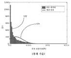
도 1a는 MTJ(100) 기반의 RNG를 예시한다. MTJ(100)는 모두 동일 선형 평면에 적층된 층들을 갖는 종래의 MTJ 디바이스이다. 상단으로부터, 제1 층은 자유 강자성층(free ferromagnetic layer)이다. 상단으로부터의 제2 층은 MgO로 형성된 절연층이다. 고정된 자기층(fixed magnetic layer)은 일반적으로 강자성 합금, 예를 들어 CoFeB로 형성된다. 상단으로부터 제3 층으로부터 시작하는 고정층은, SAF(synthetic anti-ferromagnetic) 스택(즉, 3개의 상부층 아래에 있는 층들)으로 구성된다. 상단으로부터 제3 층 아래에 있는 층들은 Ru, CoFe, AFM, 및 전극으로 형성되는 층들을 포함한다. CoFeB/Ru/CoFe의 스택은 반-강자성 교환층(anti-ferromagnetic exchange layer)(AFM)을 형성한다. 하단의 합성 SAF는 자연적 AFM에 의해 홀딩되고, PtMn 또는 IrMn 또는 유사한 합금들에 의해 형성될 수 있다.1A illustrates an MTJ (100) based RNG. The MTJ 100 is a conventional MTJ device having layers stacked in the same linear plane. From the top, the first layer is a free ferromagnetic layer. The second layer from the top is an insulating layer formed of MgO. The fixed magnetic layer is generally formed of a ferromagnetic alloy, for example CoFeB. The fixed layer starting from the third layer from the top consists of a synthetic anti-ferromagnetic (SAF) stack (i.e., the layers below the three upper layers). Layers beneath the third layer from the top include layers formed of Ru, CoFe, AFM, and electrodes. The stack of CoFeB / Ru / CoFe forms an anti-ferromagnetic exchange layer (AFM). The bottom synthetic SAF is held by a natural AFM and can be formed by PtMn or IrMn or similar alloys.
MTJ(100)를 RNG로서 작동시키기 위해, 자유 강자성층에는 전압 바이어스 Vbias가 인가되고, MTJ(100)의 타단에는 접지가 결합된다. Vbias의 인가시, MTJ(100)를 통하여 전류가 흐르고, 이 전류는 접지 단자에서 감지될 수 있다. 이 전류는 MTJ(100)가 RNG로서 동작하게 하는 랜덤 전류 특성을 갖는다. 그러나, MTJ(100)를 통한 전류에 의해 생성되는 잡음의 분포는 가우시안 분포가 아니다.To operate the
나노자석들의 다이나믹은 열 잡음에 의해 강하게 영향을 받는다. 나노자석에서의 열 잡음은 내부 이방성 필드에 대한 요동으로서 나타난다. 열 잡음은 전도 전자들의 미시적 자유도와 강자성 소자의 격자의 결과로서 고려될 수 있다. 실온 T에서, 열 잡음은 (시간 도메인 디랙-델타 자기상관을 가진) 가우시안 백색 잡음에 의해 기술된다. 잡음 필드는 자석에 대해 등방적으로 작용한다. 잡음의 존재시, LLG(Landau Lifshitz Gilbert) 방정식은 다음과 같이 기술될 수 있다.The dynamics of nanomagnets are strongly influenced by thermal noise. Thermal noise in nano-magnets appears as oscillations in the internal anisotropy field. Thermal noise can be considered as a result of the microscopic freedom of conduction electrons and the lattice of ferromagnetic elements. At room temperature T, thermal noise is described by Gaussian white noise (with time domain Dirac Delta autocorrelation). The noise field acts isotropically with respect to the magnet. In the presence of noise, the Landau Lifshitz Gilbert (LLG) equation can be described as:

내부 필드는 다음과 같이 기술된다:The internal fields are described as follows:

랜덤 열-자기 잡음의 특성들은 다음과 같다:The characteristics of the random heat-self noise are as follows:


자석들의 초기 상태들은 큰 자석 모음에서의 자기 모멘트들의 초기 각도들의 분포와 일치하도록 무작위화된다. 온도 T에서, 자석들의 초기 각도는 다음과 같다:The initial states of the magnets are randomized to coincide with the distribution of the initial angles of magnetic moments in the large magnet collection. At temperature T, the initial angle of the magnets is:

'k'는 볼츠만 상수이고, 'T'는 온도이고, Ms는 포화 자화(saturation magnetization)이고, 'V'는 부피이고, μ0는 투자율이며, Hani는 이방성 필드이다.'k' is the Boltzmann constant, 'T' is the temperature, Ms is the saturation magnetization, 'V' is the volume, μ0 is the permeability and Hani is the anisotropic field.
도 1b는 MTJ(100)로부터 감지된 랜덤 전류와, 정규 잡음 분포를 나타내는 플롯(120)을 예시한다. x축은 mA로 감지된 전류이고, y축은 전류 밀도이다. 파형(121)은 감지된 전류의 정규 분포인 한편 파형(122)은 전압 Vbias가 변경되는 것에 따른 전류 밀도이다. 플롯(120)에 도시된 바와 같이, MTJ(100)는 종-형상 가우시안 분포를 나타내지 않는다. 게다가, MTJ(100)는 변수 평균과 분산이 동적으로 변경될 수 있도록 난수 생성의 프로세스를 동적으로 제어할 수 없다.FIG. 1B illustrates a plot 120 showing the random current sensed from the
도 2는 본 개시 내용의 일 실시예에 따라, 비공선적 MTJ 디바이스(200)를 예시한다. 임의의 다른 도면의 엘리먼트들과 동일한 참조 번호들(또는 명칭들)을 갖는 도 2의 엘리먼트들은 기술된 것과 유사한 임의의 방식으로 동작하거나 기능할 수 있지만, 그러한 것에 한정되는 것은 아니라는 것을 지적한다.FIG. 2 illustrates a
일 실시예에서, 비공선적 MTJ 디바이스(200)는 서로에 대해 비공선적인 적층된 자유 및 고정 강자성층들을 포함한다. 용어 "비공선적"은 일반적으로 2개의 층이 상이한 자기 각도(magnetic angle)를 것을 지칭한다. 예를 들어, 어느 한 층이 그 자신들의 자기 각도들에 관하여 또 다른 층과 직교하는 경우, 2개의 층은 비공선적층들이다. 일 실시예에서, MTJ(200)의 비공선적 적층된 자유 및 고정 강자성층들은 MTJ(200)에 의해 감지된 전류의 정규 가우시안 분포를 생성한다. 일 실시예에서, 자유 강자성층은 고정 강자성층 크기보다 크기가 더 작다. 일 실시예에서, 한 단자가 MTJ 디바이스의 일단을 형성하는 자유 강자성층에 결합된다. 그러한 실시예에서, MTJ 디바이스의 타단은 고정 강자성층에 결합된 제2 단자를 형성한다. 일 실시예에서, 제2 단자는 접지이다.In one embodiment, the
MTJ(200)의 실시예들이 타원형 또는 원형의 적층된 층들을 예시하고 있지만, 적층된 층들은 자유 강자성층이 고정 강자성층에 관하녀 비공선적인 한 직사각형 또는 기타 형상일 수 있다. 일 실시예에서, 나노자석들의 이방성은 자유 및 고정 강자성층들의 형상에 의해 제어된다.Although embodiments of the
일 실시예에서, 자유 강자성층을 위한 Vbias를 생성하는 회로가 제공된다. 일 실시예에서, 회로는 MTJ(200)의 자석들의 자기 배리어를 제어하기 위해 Vbias의 레벨을 조정하도록 작동 가능하다. 그러한 실시예에서, Vbias의 인가로 인해 MTJ(200)에 의해 생성된 전류는 생성된 전류의 분산을 제어하는 것을 허용한다. 일 실시예에서, 회로는 Vbias를 조절함으로써 자유 강자성층을 재설정하도록 작동 가능한데, 이것은 다음 차례로 자기 배어러를 낮춘다. 일 실시예에서, MTJ(200)의 자유 강자성층에 결합된 Vbias 단자(또한 여기서는 제1 단자로도 언급된다)를 통한 전류를 감지하는 또 다른 회로가 제공된다. 일 실시예에서, 난수 발생기를 위한 시드(seed)를 제공하기 위해 감지된 전류를 디지털 표현으로 변환시키는 회로가 제공된다.In one embodiment, a circuit is provided for generating Vbias for the free ferromagnetic layer. In one embodiment, the circuit is operable to adjust the level of Vbias to control the magnetic barriers of the magnets of the
도 3은 본 개시 내용의 일 실시예에 따라, 비공선적 MTJ 디바이스(200)의 평면도(300)를 예시한다. 임의의 다른 도면의 엘리먼트들과 동일한 참조 번호들(또는 명칭들)을 갖는 도 3의 엘리먼트들은 기술된 것과 유사한 임의의 방식으로 동작하거나 기능할 수 있지만, 그러한 것에 한정되는 것은 아니라는 것을 지적한다.FIG. 3 illustrates a
이 실시예에서, 평면도(300)는 MTJ(200)의 자유 강자성층과 고정 강자성층을 나타내는 2개의 타원형/원형 형상의 객체를 나타낸다. 이 실시예에서, 자유 강자성층과 고정 강자성층 양쪽 모두는 서로에 대해 직교하며, 즉 자유 강자성층의 자기 각도 Φ2에 대한 고정 강자성층의 자기 각도 Φ1 간의 차이는 90도이다. 그러한 실시예에서, 정규 가우시안 잡음 분포가 MTJ(200) 감지 전류에서 관찰된다.In this embodiment,
일 실시예에서, MTJ의 전압 제어는 평행 구성에서 평면내 MTJ에서의 배리어의 낮춤(lowering)/튜닝(tuning)에 의해 가능하게 된다. 배리어는 다음과 같이 전압에 의해 튜닝된다:In one embodiment, the voltage control of the MTJ is enabled by a lowering / tuning of the barrier in the in-plane MTJ in a parallel configuration. The barrier is tuned by the voltage as follows:

여기서, Eb는 배리어 에너지이고,
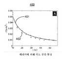
도 4a는 일 실시예에 따라, 비공선적 MTJ 디바이스에 대한 자기 배리어에 대한 자기 각도의 분산을 나타내는 플롯(400)을 예시한다. 임의의 다른 도면의 엘리먼트들과 동일한 참조 번호들(또는 명칭들)을 갖는 도 4a의 엘리먼트들은 기술된 것과 유사한 임의의 방식으로 동작하거나 기능할 수 있지만, 그러한 것에 한정되는 것은 아니라는 것을 지적한다.4A illustrates a
x축은 E/kT로 표현되는 자석의 세기이고, 여기서 'E'는 MTJ 자석들의 배리어 에너지이고, 'k'는 볼츠만 상수이며, 'T'는 온도이다. y축은 각도들의 차이의 제곱, 즉 자기 배리어 세기에 대한 각도 분산을 나타내는 (Φ2-Φ1)2이다. 여기서, 자기 각도들의 제곱에 대한 0.01은 낮은 각도 분산을 가리키는 반면 0.06은 높은 각도 분산을 가리킨다. 여기서, E/kT에 대한 10은 약한 배리어를 가리키는 반면 E/kT에 대한 50은 강한 배리어를 가리킨다. 플롯(400)은 샘플들(402)과 이 샘플들을 나타내는 매끄러운 곡선(401)을 예시한다. 플롯(400)은 자석에 대한 열 잡음의 영향을 예시한다. 각도의 분산은 배리어의 함수로서 보여진 것이다.The x-axis is the magnitude of the magnet expressed in E / kT, where 'E' is the barrier energy of the MTJ magnets, 'k' is the Boltzmann constant and 'T' is the temperature. The y-axis is the square of the difference of angles, (2 - 1)2, which represents the angular dispersion over the magnetic barrier strength. Here, 0.01 for the square of the magnetic angles indicates low angular dispersion, while 0.06 indicates high angular dispersion. Here, 10 for E / kT indicates a weak barrier whereas 50 for E / kT indicates a strong barrier.
도 4b는 일 실시예에 따라, 비공선적 MTJ 디바이스를 위한 인가된 전압에 대한 자기 배리어의 분산을 나타내는 플롯(420)을 예시한다. 임의의 다른 도면의 엘리먼트들과 동일한 참조 번호들(또는 명칭들)을 갖는 도 4b의 엘리먼트들은 기술된 것과 유사한 임의의 방식으로 동작하거나 기능할 수 있지만, 그러한 것에 한정되는 것은 아니라는 것을 지적한다.FIG. 4B illustrates a
여기서, x축은 Volt 단위의 바이어스 전압이다. 여기서, y축은 배리어의 세기를 나타내는 Eb(V)/Eb이다. 플롯(420)은 2개의 파형을 나타낸다. 파형(421)은 비-평행(anti-parallel) 자유 및 고정 강자성층들을 갖는 MTJ 디바이스의 경우와, 제1 단자에 인가된 Vbias와 자석의 배리어의 변경되는 세기 간의 대응 관계를 나타낸다. 파형(422)은 평행 자유 및 고정 강자성층들을 갖는 MTJ 디바이스의 경우와, 제1 단자에 인가된 Vbias와 자석의 배리어의 변경되는 세기 간의 대응 관계를 나타낸다. (파형들(421 및 422)의) 양쪽 경우들에서, 자유 및 고정 강자성층들은 비공선적이다. 파형들(421 및 422)은 MTJ(200)의 경우, 자기 배리어가 Vbias에 의해 튜닝될 수 있다는 것을 예시하는 것이다.Here, the x-axis is a bias voltage in Volt units. Here, the y-axis is Eb (V) / Eb representing the strength of the barrier.
도 5a는 일 실시예에 따라, 비공선적 MTJ 디바이스에 대한 잡음 전류 확률 밀도를 나타내는 플롯(500)을 예시한다. 임의의 다른 도면의 엘리먼트들과 동일한 참조 번호들(또는 명칭들)을 갖는 도 5a의 엘리먼트들은 기술된 것과 유사한 임의의 방식으로 동작하거나 기능할 수 있지만, 그러한 것에 한정되는 것은 아니라는 것을 지적한다.FIG. 5A illustrates a
여기서, x축은 정규화된 감지 전류인 한편, y축은 MTJ(200)를 통한 전류 확률 밀도이다. 플롯(500)은 정규화된 감지 전류를 나타내는 수직 막대들인 파형(501)을 예시한다. 플롯(500)은 또한 MTJ(200)에 대한 정규 가우시안 발생된 전류 확률 밀도인 파형(502)을 예시한다. 비가우시안 전류 확률을 나타내는 MTJ(100)과 비교하여, MTJ(200)는 MTJ(200)가 MTJ(100)보다 더 나은 난수 발생기로서 작동할 수 있게 하는 정규 가우시안 발생된 전류 확률 밀도를 생성한다.Here, the x-axis is the normalized sense current, while the y-axis is the current probability density through the
도 5b는 일 실시예에 따라, 비공선적 MTJ 디바이스를 위한 누적 확률 대 감지 전류를 나타내는 플롯(520)을 예시한다. 임의의 다른 도면의 엘리먼트들과 동일한 참조 번호들(또는 명칭들)을 갖는 도 5b의 엘리먼트들은 기술된 것과 유사한 임의의 방식으로 동작하거나 기능할 수 있지만, 그러한 것에 한정되는 것은 아니라는 것을 지적한다.FIG. 5B illustrates a
여기서, x축은 정규화된 감지 전류이고 y축은 MTJ(200)에 의해 생성된 잡음 전류들의 누적된 확률이다. 플롯(520)은 서로 인접하는 2개의 파형 - 파형들(521 및 522)을 예시한다. 플롯(520)은 MTJ(200)를 사용한 정규 가우시안 전류 확률의 생성을 재차 확인한다. MTJ(200)을 사용하여 생성된 잡음은 백색 잡음 프로세스에의 접촉 전력 스펙트럼 밀도 특성 또는 델타 함수 자기 상관을 가진 백색 잡음 프로세스에 의해 기술된다. 플롯(520)은 전류의 CDF(cumulative distribution function)가 가우시안 CDF를 따른다는 것을 나타낸다.Where the x-axis is the normalized sense current and the y-axis is the cumulative probability of the noise currents produced by the
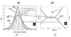
도 6의 (a) 및 (b)는 일 실시예에 따라, 비공선적 MTJ 디바이스를 위한 인가전압에 의해 자기 배리어를 변경하는 것에 의한 자기 잡음의 제어를 각기 나타내는 플롯들(600 및 620)을 예시한다. 임의의 다른 도면의 엘리먼트들과 동일한 참조 번호들(또는 명칭들)을 갖는 도 6의 (a) 및 (b)의 엘리먼트들은 기술된 것과 유사한 임의의 방식으로 동작하거나 기능할 수 있지만, 그러한 것에 한정되는 것은 아니라는 것을 지적한다. 도 6의 (a)는 MTJ(200)의 배리어 튜닝으로 인한 전압 제어에 의한 자기 각도의 분산을 예시한다. 도 6의 (b)는 MTJ(200)에 대한 인가 전압에 의한 자기 배리어의 변경을 예시한다.Figures 6A and 6B illustrate
플롯(600)의 경우, x축은 MTJ(200)를 통해 감지된 정규화된 전류인 한편 y축은 감지 전류의 확률 밀도이다. 플롯(600)은 인가된 Vbias 전압이 제로이고 자기 배리어 에너지가 40kT일 경우의 감지 전류 막대들(601)을 나타낸다. 감지 전류 막대들(602)(막대들(601)에 비해 더 짧은 막대들)은 인가된 Vbias가 0.5V이고 자기 배리어 에너지가 lOkT일 경우에 대한 것이다. 이 실시예들에서, MTJ(200)의 경우, Vbias를 생성하는 회로에 의해 이것을 조절함으로써, 전류 밀도 확률의 크기/형상이 조절되는데, 그 이유는 Vbias를 조절하는 것이 자기 배리어 세기를 조절하는 것이기 때문이다. 일 실시예에서, Vbias의 전압이 상승함에 따라, MTJ(200)의 자기 배리어 세기는 약해진다.In the case of the
파형(603)은 도 6의 (b)의 파형(621)으로 나타난 바와 같이 MTJ(200)의 비-평행 자석들에 대한 전류 잡음의 정규 가우시안 분포이다. 파형(604)은 도 6의 (b)의 파형(622)으로 나타난 바와 같이 MTJ(200)의 평행 자석들에 대한 전류 잡음의 정규 가우시안 분포이다. 플롯(620)은 자석 열 배리어가 평면내 자석들에 대한 전압의 함수로서 튜닝될 수 있다는 것을 예시하는 것이다. 파형들(621 및 622)의 형상의 변화는 MTJ(200)에서의 상이한 자석 배향에 의해 유발된다(즉, 621은 자석들이 비-평행일 경우를 나타내고 622는 자석들이 평행일 경우를 나타낸다). 실시예들에서, 인가 전압 Vbias는 자석 열 배리어의 제어를 허용하고, 이는 다음 차례로 자석의 각도 분산의 제어를 허용한다.Waveform 603 is a normal Gaussian distribution of current noise for non-parallel magnets of
도 7a 및 도 7b는 일 실시예에 따라, 고전압을 비공선적 MTJ에 인가하는 것에 의한 비공선적 MTJ 디바이스의 재설정 상태를 각기 나타내는 플롯들(700 및 720)을 예시한다. 임의의 다른 도면의 엘리먼트들과 동일한 참조 번호들(또는 명칭들)을 갖는 도 7a 및 도 7b의 엘리먼트들은 기술된 것과 유사한 임의의 방식으로 동작하거나 기능할 수 있지만, 그러한 것에 한정되는 것은 아니라는 것을 지적한다.7A and 7B illustrate
도 7a의 플롯(700)은 Vbias의 전압 레벨의 변경에 의해 MTJ(200)에서 생성된 랜덤 전류의 요동을 나타낸다. 여기서, x축은 시간이고 y축은 MTJ(200)에서 생성된 정규화된 랜덤 전류이다. 플롯(700)은 3개의 섹션 - 701, 702 및 703으로 나뉘어져 있다. 섹션(701)은 낮은 Vbias 전압에 대한 정규화된 랜덤 전류의 요동이다. 섹션(702)은 Vbias가 1V로 설정될 때 정규화된 랜덤 전류의 요동이다. 이 섹션은 MTJ(200)의 잡음 프로세스가 잡음 변수를 생성하기 위한 새로운 작동 조건(즉, 랜덤 시드)을 제공하기 위해 재설정될 수 있다는 것을 나타낸다. 여기서 용어 "재설정(reset)"은 비상관된 자기 다이나믹의 생성을 지칭한다. 섹션(703)은 Vbias가 1V보다 낮을 때 정규화된 랜덤 전류의 요동이다. 도 7b의 플롯(720)은 랜덤 변수의 위치를 무작위화하기 위한 재설정 전압의 인가를 예시하는 한편 도 7a는 최종적인 요동을 나타낸다. 여기서, 721은 반-평행 구성에 대한 배리어를 전압의 함수로서 나타내고 있는 한편, 722은 평행 구성에 대한 배리어를 전압의 함수로서 나타낸다.The
도 8은 일 실시예에 따라, 비공선적 MTJ(200) 디바이스에 의해 생성되는 전류의 전력 스펙트럼 밀도를 나타내는 플롯(800)을 예시한다. 임의의 다른 도면의 엘리먼트들과 동일한 참조 번호들(또는 명칭들)을 갖는 도 8의 엘리먼트들은 기술된 것과 유사한 임의의 방식으로 동작하거나 기능할 수 있지만, 그러한 것에 한정되는 것은 아니라는 것을 지적한다.FIG. 8 illustrates a
여기서, x축은 주파수(THz)이고 y축은 전력/주파수(dB/Hz)이다. 플롯(800)의 파형은 Vbias의 인가에 의해 MTJ(200)로부터 감지되고 및/또는 생성된 잡음 전류로부터의 백색 잡음을 나타낸다. 플롯(800)은 MTJ(200)에 의해 생성되는 전류가 넓은 주파수 범위에 걸쳐서 거의 상관이 없거나 전혀 없다는 것을 나타낸다. 이것은 MTJ(200) 디바이스가 큰 주파수 범위에 걸쳐서 난수 발생기로서 사용될 수 있다는 것을 의미한다. 일 실시예에서, MTJ 나노자석들 간의 각도는 잡음을 생성하기 위한 또 다른 제어 변수를 인에이블하도록 제조/어닐링 조건들을 통해 제어될 수 있다.Here, the x-axis is the frequency (THz) and the y-axis is the power / frequency (dB / Hz). The waveform of the
도 9는 일 실시예에 따라, 랜덤 아날로그/디지털 신호를 생성하기 위한 및 비공선적 MTJ 디바이스에 바이어스 전압을 인가하기 위한 회로(900)이다. 임의의 다른 도면의 엘리먼트들과 동일한 참조 번호들(또는 명칭들)을 갖는 도 9의 엘리먼트들은 기술된 것과 유사한 임의의 방식으로 동작하거나 기능할 수 있지만, 그러한 것에 한정되는 것은 아니라는 것을 지적한다.9 is a
일 실시예에서, 회로(900)는 LNA(low noise amplifier)(901), ADC(analog-to-digital converter), 인덕터 L, 및 커패시터 C를 포함한다. 일 실시예에서, DC(직류) 전압 Vdc가 인덕터 L의 일단에 인가된다. 일 실시예에서, 인덕터의 타단은 커패시터 C의 단자에 결합된다. 일 실시예에서, 커패시터 C의 타 단자는 LNA(901)의 입력에 결합된다. 일 실시예에서, LNA(901)의 출력은 ADC(902)의 입력에서 수신되는 랜덤 아날로그 신호이다. 일 실시예에서, LNA는 1dB 아래의 NF(잡음 지수)를 갖는다. 일 실시예에서, LNA(901)의 이득은 20-30dB의 범위이다. 기타 실시예들에서, LNA(901)에 대한 이득의 다른 값들이 이용될 수 있다. 일 실시예에서, ADC(902)의 출력은 난수를 생성하기 위해 로직 유닛에 의해 추가로 사용되는 랜덤 디지털 신호이다. 일 실시예에서, ADC(902)는 주파수 fclk를 갖는 클록 clk를 사용하여 작동한다.In one embodiment,
일 실시예에서, 인덕터 'L'의 타단과 커패시터 'C'의 일단은 MTJ(200)의 제1 단자에 결합된다. 이 실시예에서, Vdc는, 인덕터가 Vbias를 제공하는 동안 Vbias를 위한 DC 레벨을 제공한다. Vbias가 변경됨에 따라, MTJ(200) 디바이스를 통한 전류는 변경되어 Irandom 전류를 생성한다. 일 실시예에서, Irandom 전류는 정규 가우시안 전류 잡음 분포를 제공한다. 일 실시예에서, MTJ(200) 디바이스를 재설정하기 위해, Vdc는 하이 레벨로 상승된다. 일 실시예에서, MTJ(200) 디바이스의 제2 단자는 접지에 결합된다. 일 실시예에서, 접지는 RF(radio-frequency) 접지이다. 일 실시예에서, 아날로그 난수 발생기는 LNA(901)의 출력을 사용함으로써 실현된다. 일 실시예에서, 디지털 난수 발생기는 ADC(902)의 출력을 사용함으로써 실현된다.In one embodiment, one end of the inductor 'L' and one end of the capacitor 'C' are coupled to the first terminal of the
이 실시예에서, Vbias 인가 및 MTJ 전류의 대응하는 감지 모두는 회로(900)에 의해 달성된다. 기타 실시예들에서, 전류 감지는 MTJ(200) 디바이스의 접지 단자에서 수행되고, 조정가능한 Vbias는 MTJ(200) 디바이스의 제1 단자에 인가된다.In this embodiment, both the Vbias application and the corresponding sensing of the MTJ current are accomplished by the
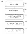
도 10은 본 개시 내용의 일 실시예에 따라, 비공선적 MTJ(200) 디바이스를 형성하는 방법의 흐름도(1000)이다. 도 10과 관련한 플로우차트에서의 블록들은 특정 순서로 도시되어 있지만, 액션들의 순서는 수정될 수 있다. 따라서, 예시된 실시예들은 상이한 순서로 실행될 수 있고, 일부 액션들/블록들은 병행하여 실행될 수 있다. 도 10에 열거된 블록들 및/또는 동작들 중 일부는 특정 실시예들에 따라 선택적이다. 제시된 블록들의 번호매김은 명료성을 위한 것이며, 다양한 블록들이 발생해야만 하는 동작들의 순서를 정의하는 것으로 의도되지는 않는다. 부가적으로, 다양한 흐름들로부터의 동작들은 다양한 조합으로 이용될 수 있다. 임의의 다른 도면의 엘리먼트들과 동일한 참조 번호들(또는 명칭들)을 갖는 도 10의 엘리먼트들은 기술된 것과 유사한 임의의 방식으로 동작하거나 기능할 수 있지만, 그러한 것에 한정되는 것은 아니라는 것을 지적한다.FIG. 10 is a flow diagram 1000 of a method of forming a
블록(1001)에서, SAF 스택이 형성되며, 즉 고정 강자성층이 형성된다. 블록(1002)에서, 자유 강자성층이 형성된다. 블록(1003)에서, SAF 스택은, 자유 강자성층과 SAF 스택이 MgO(또는 임의의 다른 절연 재료)에 의해 분리되도록 자유 강자성층에 결합된다. SAF 스택은 SAF 스택이 자유 강자성 스택에 대해 비공선적되도록 자유 강자성 스택에 결합된다. 블록(1004)에서, 제1 단자는 자유 강자성층에 결합된다. 제1 단자는 바이어스 전압을 제공하기 위해 사용된다. 블록(1005)에서, 제2 단자는 SAF 스택에 결합된다. 제2 단자는 접지에 결합된다.At
도 11은 본 개시 내용의 일 실시예에 따라, 비공선적 MTJ를 갖는 난수 발생기를 갖는 스마트 디바이스 또는 컴퓨터 시스템(1600) 또는 SoC(system-on-chip)이다. 임의의 다른 도면의 엘리먼트들과 동일한 참조 번호들(또는 명칭들)을 갖는 도 11의 엘리먼트들은 기술된 것과 유사한 임의의 방식으로 동작하거나 기능할 수 있지만, 그러한 것에 한정되는 것은 아니라는 것을 지적한다.Figure 11 is a smart device or
도 11은 플랫 표면 인터페이스 커넥터들(flat surface interface connectors)이 사용될 수 있는 모바일 디바이스의 일 실시예의 블록도를 예시한다. 일 실시예에서, 컴퓨팅 디바이스(1600)는 컴퓨팅 태블릿, 모바일폰 또는 스마트폰, 무선 가능 e-리더기 또는 다른 무선 모바일 디바이스와 같은 모바일 컴퓨팅 디바이스를 나타낸다. 특정 컴포넌트들이 일반적으로 도시되어 있으며, 이러한 디바이스의 모든 컴포넌트가 컴퓨팅 디바이스(1600)에서 도시되지는 않는다는 점이 이해될 것이다.Figure 11 illustrates a block diagram of one embodiment of a mobile device in which flat surface interface connectors may be used. In one embodiment,
일 실시예에서, 컴퓨팅 디바이스(1600)는 논의된 실시예들에 따라, 비공선적 MTJ(예를 들어, MTJ(200)) 디바이스를 갖는 난수 발생기를 갖는 제1 프로세서(1610)를 포함한다. 컴퓨팅 디바이스(1600)의 다른 블록들은 실시예들의 비공선적 MTJ 디바이스를 갖는 난수 발생기를 포함할 수 있다. 본 개시 내용의 다양한 실시예들은 시스템 실시예가 무선 디바이스, 예를 들어 셀폰 또는 PDA(personal digital assistant)에 통합될 수 있도록 무선 인터페이스와 같은 1670 내에 네트워크 인터페이스를 또한 포함할 수 있다.In one embodiment,
일 실시예에서, 프로세서(1610)(및/또는 프로세서(1690))는 마이크로프로세서들, 애플리케이션 프로세서들, 마이크로컨트롤러들, 프로그램가능 로직 디바이스들 또는 다른 처리 수단과 같은 하나 이상의 물리적 디바이스를 포함할 수 있다. 일 실시예에서, 프로세서(1690)는 선택적이다. 프로세서(1610)에 의해 실행되는 처리 동작들은, 애플리케이션 및/또는 디바이스 기능들이 실행되는 동작 플랫폼 또는 운영 체제의 실행을 포함한다. 처리 동작들은 인간 사용자나 다른 디바이스들과의 I/O(입/출력)에 연관되는 동작들, 전력 관리에 연관되는 동작들, 및/또는 컴퓨팅 디바이스(1600)를 다른 디바이스에 접속하는 것에 연관되는 동작들을 포함한다. 처리 동작들은 오디오 I/O 및/또는 디스플레이 I/O에 연관되는 동작들을 또한 포함할 수 있다.In one embodiment, processor 1610 (and / or processor 1690) may include one or more physical devices, such as microprocessors, application processors, microcontrollers, programmable logic devices or other processing means have. In one embodiment,
일 실시예에서, 컴퓨팅 디바이스(1600)는 컴퓨팅 디바이스에 오디오 기능들을 제공하는 것과 연관되는 하드웨어(예를 들어, 오디오 하드웨어 및 오디오 회로들) 및 소프트웨어(예를 들어, 드라이버들, 코덱들) 컴포넌트들을 나타내는 오디오 서브시스템(1620)을 포함한다. 오디오 기능들은 스피커 및/또는 헤드폰 출력, 뿐만 아니라 마이크로폰 입력을 포함할 수 있다. 이러한 기능들을 위한 디바이스들은 컴퓨팅 디바이스(1600)에 통합되거나, 또는 컴퓨팅 디바이스(1600)에 접속될 수 있다. 일 실시예에서, 사용자는 프로세서(1610)에 의해 수신되고 처리되는 오디오 명령들을 제공함으로써 컴퓨팅 디바이스(1600)와 상호작용한다.In one embodiment,
디스플레이 서브시스템(1630)은 사용자가 컴퓨팅 디바이스(1600)와 상호작용하기 위한 시각적 및/또는 촉각적 디스플레이를 제공하는 하드웨어(예를 들어, 디스플레이 디바이스들) 및 소프트웨어(예를 들어, 드라이버들) 컴포넌트들을 나타낸다. 디스플레이 서브시스템(1630)은 사용자에게 디스플레이를 제공하기 위해 사용되는 특정 스크린 또는 하드웨어 디바이스를 포함하는 디스플레이 인터페이스(1632)를 포함한다. 일 실시예에서, 디스플레이 인터페이스(1632)는 프로세서(1610)와는 별개이며 디스플레이에 연관되는 적어도 일부 처리를 실행하기 위한 로직을 포함한다. 일 실시예에서, 디스플레이 서브시스템(1630)은 사용자에게 출력 및 입력 양쪽 모두를 제공하는 터치 스크린(또는 터치 패드) 디바이스를 포함한다.
I/O 제어기(1640)는 사용자와의 상호작용에 연관되는 하드웨어 디바이스들 및 소프트웨어 컴포넌트들을 나타낸다. I/O 제어기(1640)는 오디오 서브시스템(1620) 및/또는 디스플레이 서브시스템(1630)의 일부인 하드웨어를 관리하도록 동작 가능하다. 부가적으로, I/O 제어기(1640)는 사용자가 시스템과 상호작용할 수 있는 컴퓨팅 디바이스(1600)에 접속하는 부가적인 디바이스들에 대한 접속 포인트를 예시한다. 예를 들어, 컴퓨팅 디바이스(1600)에 부착될 수 있는 디바이스들로는, 마이크로폰 디바이스들, 스피커, 또는 스테레오 시스템들, 비디오 시스템들 또는 기타의 디스플레이 디바이스들, 키보드, 또는 키패드 디바이스들, 또는 카드 리더기들 또는 기타의 디바이스들 등의 특정한 애플리케이션들에서 사용하기 위한 기타의 I/O 디바이스들이 포함될 수 있다.I /
앞서 언급된 바와 같이, I/O 제어기(1640)는 오디오 서브시스템(1620) 및/또는 디스플레이 서브시스템(1630)과 상호작용할 수 있다. 예를 들어, 입력은 마이크로폰 또는 다른 오디오 디바이스를 통하여 하나 이상의 애플리케이션들 또는 컴퓨팅 디바이스(1600)의 기능들에게 입력 또는 명령들을 제공할 수 있다. 부가적으로, 오디오 출력이 디스플레이 출력 대신에 또는 디스플레이 출력에 부가하여 제공될 수 있다. 다른 예에서, 디스플레이 서브시스템(1630)이 터치 스크린을 포함하는 경우, 디스플레이 디바이스는 또한 I/O 제어기(1640)에 의해 적어도 부분적으로 관리될 수 있는 입력 디바이스의 역할을 한다. I/O 제어기(1640)에 의해 관리되는 I/O 기능들을 제공하기 위한 부가적인 버튼들 또는 스위치들이 컴퓨팅 디바이스(1600) 상에 또한 존재할 수 있다.As noted above, the I /
일 실시예에서, I/O 제어기(1640)는 가속도계들, 카메라들, 광 센서들 또는 다른 환경 센서들, 또는 컴퓨팅 디바이스(1600)에 포함될 수 있는 다른 하드웨어와 같은 디바이스들을 관리한다. 입력은 직접 사용자 상호작용의 일부일 뿐만 아니라, 그것의 동작들(예컨대, 잡음의 필터링, 밝기 검출을 위한 디스플레이들의 조정, 카메라용 플래시 적용, 또는 다른 특징들)에 영향을 주기 위한 시스템에 환경적 입력을 제공하는 것일 수 있다.In one embodiment, the I /
일 실시예에서, 컴퓨팅 디바이스(1600)는 배터리 전력 사용, 배터리의 충전, 및 전력 절감 동작에 연관되는 특징들을 관리하는 전력 관리(1650)를 포함한다. 메모리 서브시스템(1660)은 컴퓨팅 디바이스(1600)에 정보를 저장하기 위한 메모리 디바이스들을 포함한다. 메모리는 비휘발성(메모리 디바이스에 대한 전력이 중단되는 경우에 상태가 변경되지 않음) 및/또는 휘발성(메모리 디바이스에 대한 전력이 중단되는 경우에 상태가 정의되지 않음(indeterminate)) 메모리 디바이스들을 포함할 수 있다. 메모리 서브시스템(1660)은 애플리케이션 데이터, 사용자 데이터, 음악, 사진, 문서, 또는 다른 데이터 뿐만 아니라 컴퓨팅 디바이스(1600)의 애플리케이션들 및 기능들의 실행과 연관되는 시스템 데이터(장기적이거나 임시적임)를 저장할 수 있다.In one embodiment,
실시예들의 엘리먼트들은 컴퓨터 실행가능 명령어들(예를 들어, 본 명세서에서 논의되는 임의의 다른 프로세스들을 구현하는 명령어들)을 저장하기 위한 머신 판독가능 매체(예를 들어, 메모리(1660))로서 또한 제공된다. 이러한 머신 판독가능 매체(예를 들어, 메모리(1660))는, 플래시 메모리, 광 디스크들, CD-ROM들, DVD ROM들, RAM들, EPROM들, EEPROM들, 자기 또는 광학 카드들, PCM(Phase Change Memory), 또는 전자적 또는 컴퓨터 실행가능 명령어들을 저장하기에 적합한 다른 유형들의 머신 판독가능 매체를 포함할 수 있지만, 이에 제한되는 것은 아니다. 예를 들어, 본 개시 내용의 실시예들은 원격 컴퓨터(예를 들어, 서버)로부터 요청 컴퓨터(예를 들어, 클라이언트)로 통신 링크(예를 들어, 모뎀 또는 네트워크 접속)를 통하여 데이터 신호에 의해 전송될 수 있는 컴퓨터 프로그램(예를 들어, BIOS)으로서 다운로드될 수 있다.The elements of embodiments may be implemented as a machine-readable medium (e.g., memory 1660) for storing computer-executable instructions (e.g., instructions that implement any other processes discussed herein) / RTI > Such a machine-readable medium (e.g., memory 1660) may comprise one or more of a flash memory, optical disks, CD-ROMs, DVD ROMs, RAMs, EPROMs, EEPROMs, magnetic or optical cards, Phase Change Memory), or any other type of machine-readable medium suitable for storing electronic or computer-executable instructions. For example, embodiments of the present disclosure may be embodied in a computer-readable medium, such as a computer-readable medium, for example, (E. G., A BIOS) that can be downloaded to the computer.
접속성(connectivity)(1670)은 컴퓨팅 디바이스(1600)가 외부 디바이스들과 통신하는 것을 가능하게 하기 위한 하드웨어 디바이스들(예를 들어, 무선 및/또는 유선 커넥터들 및 통신 하드웨어) 및 소프트웨어 컴포넌트들(예를 들어, 드라이버들, 프로토콜 스택들)을 포함한다. 컴퓨팅 디바이스(1600)는 헤드셋들, 프린터들, 또는 다른 디바이스들과 같은 주변 장치들뿐만 아니라, 다른 컴퓨팅 디바이스들, 무선 액세스 포인트들 또는 기지국들과 같은 별개의 디바이스들일 수 있다.
접속성(1670)은 복수의 상이한 유형의 접속성을 포함할 수 있다. 일반화하기 위해서, 컴퓨팅 디바이스(1600)는 셀룰러 접속성(1672) 및 무선 접속성(1674)을 갖는 것으로 예시되어 있다. 일반적으로, 셀룰러 접속성(1672)은 무선 캐리어들에 의해 제공되는, 예컨대 GSM(global system for mobile communications) 또는 변형물들이나 파생물들, CDMA(code division multiple access) 또는 변형물들이나 파생물들, TDM(time division multiplexing) 또는 변형물들이나 파생물들, 또는 다른 셀룰러 서비스 표준들을 통해 제공되는 셀룰러 네트워크 접속성을 지칭한다. 무선 접속성(또는 무선 인터페이스)(1674)은 셀룰러가 아닌 무선 접속성을 지칭하며, (블루투스, 근접장(Near Field) 등과 같은) 개인 영역 네트워크들, (Wi-Fi와 같은) 로컬 영역 네트워크들, 및/또는 (WiMax와 같은) 광역 네트워크들, 또는 다른 무선 통신을 포함할 수 있다.
주변 장치 접속들(peripheral connections)(1680)은 주변 장치 접속들을 구축하기 위한 하드웨어 인터페이스들과 커넥터들뿐만 아니라 소프트웨어 컴포넌트들(예를 들어, 드라이버들, 프로토콜 스택들)을 포함한다. 컴퓨팅 디바이스(1600)는 다른 컴퓨팅 디바이스로의 주변 장치("로"(1682))일 수 있는 것은 물론, 자신에 접속되는 주변 장치("로부터의"(1684))를 가질 수 있다는 점을 이해할 것이다. 컴퓨팅 디바이스(1600)는 흔히, 컴퓨팅 디바이스(1600) 상에서 콘텐츠를 관리(예를 들어, 다운로딩 및/또는 업로딩, 변경, 동기화)하는 것 등의 목적을 위해 다른 컴퓨팅 디바이스에 접속하기 위한 "도킹" 커넥터를 갖는다. 부가적으로, 도킹 커넥터는 컴퓨팅 디바이스(1600)가 예를 들어 시청각 시스템 또는 다른 시스템에 대한 콘텐츠 출력을 제어할 수 있게 하는 특정 주변 장치들에 컴퓨팅 디바이스(1600)가 접속하는 것을 허용할 수 있다.
사유 도킹 커넥터(proprietary docking connector) 또는 다른 사유 접속 하드웨어에 부가하여, 컴퓨팅 디바이스(1600)는 공통 또는 표준 기반 커넥터들을 통해 주변 장치 접속들(1680)을 구축할 수 있다. 흔한 유형들은 USB 커넥터(이것은 복수의 상이한 하드웨어 인터페이스들 중 임의의 것을 포함할 수 있음), MDP(MiniDisplayPort)를 포함하는 DisplayPort, HDMI(High Definition Multimedia Interface), 파이어와이어, 또는 다른 유형을 포함할 수 있다.In addition to a proprietary docking connector or other private access hardware, the
본 명세서에서 "실시예", "일 실시예', "일부 실시예", 또는 "기타 실시예"라는 언급은, 실시예들과 연계하여 설명된 특정한 특징, 구조, 또는 특성이, 반드시 모든 실시예가 아니라, 적어도 일부 실시예에 포함된다는 것을 의미한다. "실시예", "일 실시예", 또는 "일부 실시예"의 다양한 등장들은 모두가 반드시 동일 실시예를 참조하는 것은 아니다. 명세서에서 컴포넌트, 특징, 구조, 또는 특성이 "포함될 수도(may, might)", 또는 "포함될 수(could)" 있다고 진술한다면, 그 특정한 컴포넌트, 특징, 구조, 또는 특성은 포함될 것이 요구되는 것은 아니다. 명세서 또는 청구항에서 "한(a, an)" 엘리먼트를 언급한다면, 이것은 그 엘리먼트가 단 하나만 있다는 것을 의미하는 것은 아니다. 명세서 또는 청구항에서 "추가적(additional)" 엘리먼트를 언급한다면, 이것은 하나보다 많은 추가적 엘리먼트가 있다는 것을 배제하지 않는다.Reference herein to "an embodiment," " an embodiment, "" some embodiments," or "other embodiments" means that a particular feature, structure, or characteristic described in connection with the embodiments Quot ;, " an embodiment ", or "an embodiment" does not necessarily refer to the same embodiment. , Feature, structure, or characteristic is not intended to be " comprising, " or that a particular feature, structure, or characteristic may be " When referring to an " an "element in a claim, this does not mean that there is only one such element. It does not exclude that there are many additional elements.
또한, 특정 특징들, 구조들, 기능들, 또는 특성들은 하나 이상의 실시예에서 임의의 적합한 방식으로 결합될 수 있다. 예를 들어, 2개의 실시예와 연관되는 특정 특징들, 구조들, 기능들, 또는 특성들이 상호 배타적이지 않은 임의의 경우에 제1 실시예는 제2 실시예와 결합될 수 있다.Furthermore, certain features, structures, functions, or characteristics may be combined in any suitable manner in one or more embodiments. For example, the first embodiment may be combined with the second embodiment in any case where the particular features, structures, functions, or characteristics associated with the two embodiments are not mutually exclusive.
본 개시 내용은 그것의 특정 실시예들과 관련하여 설명되었지만, 전술한 설명에 비추어, 관련 기술분야의 통상의 기술자에게 이 실시예들의 많은 대안물, 수정물, 및 변형물이 명백할 것이다. 예를 들어, 다른 메모리 아키텍처들, 예를 들어 동적 RAM(DRAM)이 논의된 실시예들을 이용할 수 있다. 본 개시 내용의 실시예들은 첨부 청구항들의 넓은 범위 내에 있는 이러한 모든 대안물, 수정물, 및 변형물을 포괄하는 것으로 의도된다.While this disclosure has been described in connection with specific embodiments thereof, many alternatives, modifications, and variations of these embodiments will be apparent to those of ordinary skill in the art in light of the foregoing description. For example, other memory architectures, such as dynamic random access memory (DRAM), may use the discussed embodiments. The embodiments of the present disclosure are intended to embrace all such alternatives, modifications, and variations that fall within the broad scope of the appended claims.
또한, 집적 회로(IC) 칩들 및 다른 컴포넌트들에 대한 잘 알려진 전력/접지 접속들은, 예시, 및 논의의 단순화를 위해 및 본 개시 내용을 모호하게 하지 않도록, 제시된 도면들 내에 도시될 수도 있고 도시되지 않을 수도 있다. 또한, 배열들은 본 개시 내용을 모호하게 하는 것을 회피하기 위해서 블록도 형태로 도시될 수 있고, 이러한 블록도 배열들의 구현과 관련한 상세들이 본 개시 내용이 구현되어야 하는 플랫폼에 크게 종속한다(즉, 이러한 상세들은 관련 기술분야의 통상의 기술자의 범위 내에 있어야 한다)는 사실을 고려하여 배열들은 또한 블록도 형태로 도시될 수 있다. 본 개시 내용의 예시적 실시예들을 설명하기 위해서 특정 상세들(예를 들어, 회로들)이 제시되어 있지만, 본 개시 내용은 이들 특정 상세들 없이 또는 이들 특정 상세들의 변형물을 이용하여 실시될 수 있다는 것이 관련 기술분야의 통상의 기술자에게 명백할 것이다. 따라서, 본 설명은 제한하는 것 대신에 예시적 것으로 간주되어야 한다.In addition, well known power / ground connections to integrated circuit (IC) chips and other components may be shown in and / or shown in the drawings so as not to obscure the present disclosure for simplicity of illustration, and discussion . Arrangements may also be illustrated in block diagram form in order to avoid obscuring the present disclosure, and details regarding the implementation of such block diagram arrays are largely dependent upon the platform on which this disclosure is to be implemented (i.e., The details should be within the scope of ordinary skill in the relevant art), the arrays may also be shown in block diagram form. Although specific details (e.g., circuits) have been set forth to illustrate exemplary embodiments of the present disclosure, the present disclosure may be practiced without these specific details or with variations of these specific details Will be apparent to those of ordinary skill in the art. Accordingly, the description is to be regarded as illustrative instead of restrictive.
하기 예들은 추가 실시예들과 관련된다. 이 예들에서의 상세들은 하나 이상의 실시예에서의 어디에서나 이용될 수 있다. 본 명세서에 설명된 장치의 모든 선택적인 특징들은 방법 또는 프로세스와 관련하여 또한 구현될 수 있다.The following examples relate to additional embodiments. Details in these examples may be used anywhere in one or more embodiments. All optional features of the apparatus described herein may also be implemented in connection with a method or process.
예를 들어, 일 실시예에서, 장치는 자유 강자성층; 자유 강자성층에 대해 비공선적 방향에 위치한 고정 강자성층; 및 자유 강자성층에 결합되어, 자유 강자성층에 바이어스 전압을 제공하는 제1 단자를 포함한다. 일 실시예에서, 장치는 고정 강자성층에 결합된 제2 단자를 더 포함한다. 일 실시예에서, 제2 단자는 접지에 결합된다.For example, in one embodiment, the apparatus includes a free ferromagnetic layer; A stationary ferromagnetic layer positioned in the non-conductive direction with respect to the free ferromagnetic layer; And a first terminal coupled to the free ferromagnetic layer to provide a bias voltage to the free ferromagnetic layer. In one embodiment, the apparatus further comprises a second terminal coupled to the fixed ferromagnetic layer. In one embodiment, the second terminal is coupled to ground.
일 실시예에서, 장치는 조정가능한 전압 레벨을 가진 바이어스 전압을 생성하는 회로를 더 포함한다. 일 실시예에서, 회로는 바이어스 전압을 조절함으로써 자유 강자성층을 재설정하도록 동작 가능하다. 일 실시예에서, 회로는 바이어스 전압을 조절함으로써 제1 단자를 통한 전류를 무작위화하도록 동작 가능하다. 일 실시예에서, 자유 강자성층과 고정 강자성층은 적층된 평면내 MTJ(magnetic tunnel junction) 디바이스를 형성한다.In one embodiment, the apparatus further comprises circuitry for generating a bias voltage having an adjustable voltage level. In one embodiment, the circuit is operable to reset the free ferromagnetic layer by adjusting the bias voltage. In one embodiment, the circuit is operable to randomize the current through the first terminal by adjusting the bias voltage. In one embodiment, the free ferromagnetic layer and the fixed ferromagnetic layer form a stacked planar magnetic tunnel junction (MTJ) device.
일 실시예에서, 장치는 제1 단자를 통한 전류를 감지하는 전류 센서를 더 포함하고, 전류는 바이어스 전압으로 인해 생성된다. 일 실시예에서, 자유 강자성층은 고정 강자성층에 대해 90도로 위치된다.In one embodiment, the apparatus further comprises a current sensor for sensing current through the first terminal, wherein the current is generated due to the bias voltage. In one embodiment, the free ferromagnetic layer is positioned at 90 degrees relative to the fixed ferromagnetic layer.
다른 예에서, 일 실시예에서, 메모리; 메모리에 결합되며, 상술한 장치를 갖는 프로세서; 및 프로세서가 또 다른 디바이스와 통신할 수 있게 하는 무선 인터페이스를 포함하는 시스템이 제공된다.In another example, in one embodiment, a memory; A processor coupled to the memory and having the apparatus described above; And a wireless interface that allows the processor to communicate with another device.
다른 예에서, 비공선형으로 위치하는 자유 및 고정 강자성층들을 갖는 MTJ(magnetic tunnel junction) 디바이스; 및 자유 강자성층에 조정가능한 바이어스 전압을 제공하여, MTJ 디바이스에 의해 감지된 전류의 분산을 제어하는 회로를 포함하는, 난수 발생기를 갖는 집적 회로가 제공된다. 일 실시예에서, 집적 회로는 자유 강자성층에 결합되어 조정가능한 바이어스 전압을 수신하는 제1 단자를 더 포함한다.In another example, a magnetic tunnel junction (MTJ) device having free and stationary ferromagnetic layers positioned non-linearly; And an integrated circuit having a random number generator comprising circuitry for providing an adjustable bias voltage to the free ferromagnetic layer to control the dispersion of the current sensed by the MTJ device. In one embodiment, the integrated circuit further includes a first terminal coupled to the free ferromagnetic layer to receive an adjustable bias voltage.
일 실시예에서, 집적 회로는 제1 단자를 통한 전류를 감지하는 전류 센서를 더 포함하고, 전류는 상기 바이어스 전압으로 인해 생성된다. 일 실시예에서, 회로는 바이어스 전압을 조절함으로써 자유 강자성층을 재설정하도록 동작 가능하다. 일 실시예에서, 회로는 바이어스 전압을 조절함으로써 제1 단자를 통한 전류를 무작위화하도록 동작 가능하다. 일 실시예에서, 자유 강자성층은 고정 강자성층에 대해 90도로 위치된다.In one embodiment, the integrated circuit further comprises a current sensor for sensing current through the first terminal, and a current is generated due to the bias voltage. In one embodiment, the circuit is operable to reset the free ferromagnetic layer by adjusting the bias voltage. In one embodiment, the circuit is operable to randomize the current through the first terminal by adjusting the bias voltage. In one embodiment, the free ferromagnetic layer is positioned at 90 degrees relative to the fixed ferromagnetic layer.
다른 예에서, 일 실시예에서, 메모리; 메모리에 결합되며, 상술한 집적 회로에 따른 난수 발생기를 갖는 집적 회로; 및 프로세서가 또 다른 디바이스와 통신할 수 있게 하는 무선 인터페이스를 포함하는 시스템이 제공된다.In another example, in one embodiment, a memory; An integrated circuit coupled to the memory and having a random number generator according to the integrated circuit described above; And a wireless interface that allows the processor to communicate with another device.
독자가 본 기술적 개시 내용의 속성 및 요점을 알아내는 것을 허용하는 요약서가 제공된다. 이 요약서는 이것이 청구항들의 범위나 의미를 제한하기 위해 이용되지는 않을 것이라는 이해와 함께 제출된다. 다음의 청구항들은 이로써 상세한 설명에 포함되며, 각각의 청구항은 별개의 실시예로서 자립한다.An abstract is provided that allows the reader to determine the nature and point of the technical disclosure. This summary is presented with the understanding that it will not be used to limit the scope or meaning of the claims. The following claims are hereby incorporated into the Detailed Description and each claim is self-sustaining as a separate embodiment.
Claims (19)
Translated fromKorean자유 강자성층(free ferromagnetic layer);
상기 자유 강자성층에 대해 비공선적 방향(non-collinear direction)에 위치한 고정 강자성층; 및
상기 자유 강자성층에 결합되어, 상기 자유 강자성층에 바이어스 전압을 제공하는 제1 단자
를 포함하는 장치.As an apparatus,
A free ferromagnetic layer;
A fixed ferromagnetic layer located in a non-collinear direction with respect to the free ferromagnetic layer; And
And a second ferromagnetic layer coupled to the free ferromagnetic layer and providing a bias voltage to the free ferromagnetic layer,
/ RTI >
상기 고정 강자성층에 결합된 제2 단자를 더 포함하는 장치.The method according to claim 1,
And a second terminal coupled to the fixed ferromagnetic layer.
상기 제2 단자는 접지에 결합되는, 장치.3. The method of claim 2,
And the second terminal is coupled to ground.
조정가능한 전압 레벨을 갖는 상기 바이어스 전압을 생성하는 회로를 더 포함하는 장치.The method according to claim 1,
Further comprising circuitry for generating the bias voltage having an adjustable voltage level.
상기 회로는 상기 바이어스 전압을 조절함으로써 상기 자유 강자성층을 재설정하도록 동작 가능한, 장치.5. The method of claim 4,
Wherein the circuit is operable to reset the free ferromagnetic layer by adjusting the bias voltage.
상기 회로는 상기 바이어스 전압을 조절함으로써 상기 제1 단자를 통한 전류를 무작위화하도록 동작 가능한, 장치.5. The method of claim 4,
Wherein the circuit is operable to randomize the current through the first terminal by adjusting the bias voltage.
상기 자유 강자성층과 상기 고정 강자성층은 적층된 평면내 MTJ(magnetic tunnel junction) 디바이스를 형성하는, 장치.The method according to claim 1,
Wherein the free ferromagnetic layer and the fixed ferromagnetic layer form a stacked planar magnetic tunnel junction (MTJ) device.
상기 제1 단자를 통한 전류를 감지하는 전류 센서를 더 포함하고, 상기 전류는 상기 바이어스 전압으로 인해 생성되는 장치.The method according to claim 1,
Further comprising a current sensor for sensing a current through the first terminal, wherein the current is generated due to the bias voltage.
상기 자유 강자성층은 상기 고정 강자성층에 대해 90도로 위치되는, 장치.The method according to claim 1,
And the free ferromagnetic layer is positioned at 90 degrees relative to the fixed ferromagnetic layer.
비공선형으로 위치하는 자유 강자성층 및 고정 강자성층을 갖는 MTJ(magnetic tunnel junction) 디바이스; 및
상기 자유 강자성층에 조정가능한 바이어스 전압을 제공하는 회로 - 상기 회로는 상기 MTJ 디바이스에 의해 감지된 전류의 분산(variance)을 제어함 -
를 포함하는 집적 회로.An integrated circuit having a random number generator,
A magnetic tunnel junction (MTJ) device having a free ferromagnetic layer and a fixed ferromagnetic layer positioned in a non-aligned state; And
Circuitry for providing an adjustable bias voltage to said free ferromagnetic layer, said circuitry controlling the variance of the current sensed by said MTJ device,
≪ / RTI >
상기 자유 강자성층에 결합되어 상기 조정가능한 바이어스 전압을 수신하는 제1 단자를 더 포함하는 집적 회로.11. The method of claim 10,
And a first terminal coupled to the free ferromagnetic layer to receive the adjustable bias voltage.
상기 제1 단자를 통한 전류를 감지하는 전류 센서를 더 포함하고, 상기 전류는 상기 바이어스 전압으로 인해 생성되는 집적 회로.12. The method of claim 11,
Further comprising a current sensor for sensing current through the first terminal, wherein the current is generated due to the bias voltage.
상기 회로는 상기 바이어스 전압을 조절함으로써 상기 자유 강자성층을 재설정하도록 동작 가능한, 집적 회로.11. The method of claim 10,
Wherein the circuit is operable to reset the free ferromagnetic layer by adjusting the bias voltage.
상기 회로는 상기 바이어스 전압을 조절함으로써 상기 제1 단자를 통한 전류를 무작위화하도록 동작 가능한, 집적 회로.11. The method of claim 10,
Wherein the circuit is operable to randomize the current through the first terminal by adjusting the bias voltage.
상기 자유 강자성층은 상기 고정 강자성층에 대해 90도로 위치되는, 집적 회로.11. The method of claim 10,
Wherein the free ferromagnetic layer is positioned at 90 degrees relative to the fixed ferromagnetic layer.
메모리;
상기 메모리에 결합되며, 제1항 내지 제9항 중 어느 한 항의 장치를 갖는 프로세서; 및
상기 프로세서가 또 다른 디바이스와 통신할 수 있게 하는 무선 인터페이스
를 포함하는 시스템.As a system,
Memory;
A processor coupled to the memory and having the apparatus of any one of claims 1 to 9; And
A wireless interface that allows the processor to communicate with another device
/ RTI >
디스플레이 유닛을 더 포함하는 시스템.17. The method of claim 16,
≪ / RTI > further comprising a display unit.
상기 디스플레이 유닛은 터치 스크린인, 시스템.18. The method of claim 17,
Wherein the display unit is a touch screen.
메모리;
상기 메모리에 결합되며, 제10항 내지 제15항 중 어느 한 항의 집적 회로에 따른 난수 발생기를 갖는 프로세서; 및
상기 프로세서가 또 다른 디바이스와 통신할 수 있게 하는 무선 인터페이스
를 포함하는 시스템.As a system,
Memory;
A processor coupled to the memory and having a random number generator according to the integrated circuit of any one of claims 10 to 15; And
A wireless interface that allows the processor to communicate with another device
/ RTI >
Applications Claiming Priority (1)
| Application Number | Priority Date | Filing Date | Title |
|---|---|---|---|
| PCT/US2013/062378WO2015047328A1 (en) | 2013-09-27 | 2013-09-27 | Voltage controlled nano-magnetic random number generator |
Publications (1)
| Publication Number | Publication Date |
|---|---|
| KR20160061316Atrue KR20160061316A (en) | 2016-05-31 |
Family
ID=52744228
Family Applications (1)
| Application Number | Title | Priority Date | Filing Date |
|---|---|---|---|
| KR1020167004713ACeasedKR20160061316A (en) | 2013-09-27 | 2013-09-27 | Voltage controlled nano-magnetic random number generator |
Country Status (7)
| Country | Link |
|---|---|
| US (1) | US20160202954A1 (en) |
| EP (1) | EP3050132A4 (en) |
| KR (1) | KR20160061316A (en) |
| CN (1) | CN104516712B (en) |
| DE (1) | DE102014014233A1 (en) |
| TW (1) | TWI544405B (en) |
| WO (1) | WO2015047328A1 (en) |
Cited By (3)
| Publication number | Priority date | Publication date | Assignee | Title |
|---|---|---|---|---|
| US10042609B2 (en) | 2014-05-09 | 2018-08-07 | Quantum Numbers Corp. | Method for generating random numbers and associated random number generator |
| US10430160B2 (en) | 2018-01-15 | 2019-10-01 | Quantum Numbers Corp. | Method and system for generating a random bit sample |
| US11366639B2 (en) | 2018-05-11 | 2022-06-21 | Electronics And Telecommunications Research Institute | Apparatus and method for generating quantum random number |
Families Citing this family (11)
| Publication number | Priority date | Publication date | Assignee | Title |
|---|---|---|---|---|
| US9459835B2 (en)* | 2014-01-15 | 2016-10-04 | HGST Netherlands B.V. | Random number generator by superparamagnetism |
| US9547476B2 (en) | 2014-10-15 | 2017-01-17 | The United States Of America, As Represented By The Secretary Of The Army | Semiconductor-junction-derived random number generation with triggering mechanism |
| EP3051411B1 (en)* | 2015-01-27 | 2018-05-16 | Neopost Technologies | Hardware non-deterministic random byte generator |
| WO2016204750A1 (en)* | 2015-06-17 | 2016-12-22 | Intel Corporation | Random number generator |
| US10127016B2 (en)* | 2016-01-22 | 2018-11-13 | Nanyang Technological University | Magnetic random number generator |
| US10225082B2 (en) | 2016-07-26 | 2019-03-05 | International Business Machines Corporation | Carbon nanotube physical entropy source |
| GB2548428B (en)* | 2016-08-08 | 2018-05-16 | Quantum Base Ltd | Nondeterministic response to a challenge |
| US10078496B2 (en) | 2017-02-23 | 2018-09-18 | International Business Machines Corporation | Magnetic tunnel junction (MTJ) based true random number generators (TRNG) |
| JP7549891B2 (en)* | 2019-07-03 | 2024-09-12 | 国立大学法人東北大学 | Random Number Generation Unit and Computing System |
| US11209505B2 (en)* | 2019-08-26 | 2021-12-28 | Western Digital Technologies, Inc. | Large field range TMR sensor using free layer exchange pinning |
| CN112558925A (en)* | 2020-12-15 | 2021-03-26 | 中国科学院上海微系统与信息技术研究所 | Random number generating unit and random number generator |
Family Cites Families (14)
| Publication number | Priority date | Publication date | Assignee | Title |
|---|---|---|---|---|
| US6088450A (en)* | 1996-04-17 | 2000-07-11 | Intel Corporation | Authentication system based on periodic challenge/response protocol |
| JP2000066592A (en)* | 1998-08-19 | 2000-03-03 | Syst Kogaku Kk | Random number generator |
| US7911832B2 (en)* | 2003-08-19 | 2011-03-22 | New York University | High speed low power magnetic devices based on current induced spin-momentum transfer |
| US7973349B2 (en)* | 2005-09-20 | 2011-07-05 | Grandis Inc. | Magnetic device having multilayered free ferromagnetic layer |
| US7777261B2 (en)* | 2005-09-20 | 2010-08-17 | Grandis Inc. | Magnetic device having stabilized free ferromagnetic layer |
| US7692503B2 (en)* | 2007-03-23 | 2010-04-06 | Intel Corporation | Random number generator based on oscillator noise |
| US8495118B2 (en)* | 2008-10-30 | 2013-07-23 | Seagate Technology Llc | Tunable random bit generator with magnetic tunnel junction |
| US8257596B2 (en)* | 2009-04-30 | 2012-09-04 | Everspin Technologies, Inc. | Two-axis magnetic field sensor with substantially orthogonal pinning directions |
| JP2011013901A (en)* | 2009-07-01 | 2011-01-20 | Sony Corp | Random number generator |
| JP2011113136A (en)* | 2009-11-24 | 2011-06-09 | Sony Corp | Random number generating device, random number generation method, and security chip |
| US8423329B2 (en)* | 2010-01-21 | 2013-04-16 | Qualcomm Incorporated | System and method of adjusting a resistance-based memory circuit parameter |
| US8427197B2 (en)* | 2011-06-15 | 2013-04-23 | Honeywell International Inc. | Configurable reference circuit for logic gates |
| US9189201B2 (en)* | 2011-09-20 | 2015-11-17 | Qualcomm Incorporated | Entropy source with magneto-resistive element for random number generator |
| KR101874408B1 (en)* | 2011-11-09 | 2018-07-05 | 삼성전자주식회사 | Nonvolatile memory device and memory system including the same |
- 2013
- 2013-09-27KRKR1020167004713Apatent/KR20160061316A/ennot_activeCeased
- 2013-09-27USUS14/912,895patent/US20160202954A1/ennot_activeAbandoned
- 2013-09-27EPEP13894219.8Apatent/EP3050132A4/ennot_activeWithdrawn
- 2013-09-27WOPCT/US2013/062378patent/WO2015047328A1/enactiveApplication Filing
- 2014
- 2014-09-15TWTW103131744Apatent/TWI544405B/enactive
- 2014-09-26DEDE102014014233.7Apatent/DE102014014233A1/ennot_activeWithdrawn
- 2014-09-26CNCN201410504791.1Apatent/CN104516712B/ennot_activeExpired - Fee Related
Cited By (4)
| Publication number | Priority date | Publication date | Assignee | Title |
|---|---|---|---|---|
| US10042609B2 (en) | 2014-05-09 | 2018-08-07 | Quantum Numbers Corp. | Method for generating random numbers and associated random number generator |
| US10437559B2 (en) | 2014-05-09 | 2019-10-08 | Quantum Numbers Corp. | Method for generating random numbers and associated random number generator |
| US10430160B2 (en) | 2018-01-15 | 2019-10-01 | Quantum Numbers Corp. | Method and system for generating a random bit sample |
| US11366639B2 (en) | 2018-05-11 | 2022-06-21 | Electronics And Telecommunications Research Institute | Apparatus and method for generating quantum random number |
Also Published As
| Publication number | Publication date |
|---|---|
| TW201531936A (en) | 2015-08-16 |
| US20160202954A1 (en) | 2016-07-14 |
| DE102014014233A1 (en) | 2015-04-02 |
| CN104516712B (en) | 2018-11-20 |
| EP3050132A1 (en) | 2016-08-03 |
| WO2015047328A1 (en) | 2015-04-02 |
| TWI544405B (en) | 2016-08-01 |
| CN104516712A (en) | 2015-04-15 |
| EP3050132A4 (en) | 2017-05-24 |
Similar Documents
| Publication | Publication Date | Title |
|---|---|---|
| KR20160061316A (en) | Voltage controlled nano-magnetic random number generator | |
| TWI610473B (en) | Coupled spin Hall nm oscillator with adjustable intensity | |
| KR102416979B1 (en) | random number generator | |
| CN106688041B (en) | Strain-Assisted Spin Torque Flip Spin Transfer Torque Memory | |
| US9620188B2 (en) | MTJ spin hall MRAM bit-cell and array | |
| CN107534082B (en) | XOR logic device with spin orbit torque effect | |
| CN107004759B (en) | Magnetoelectric Devices and Interconnects | |
| WO2019125684A1 (en) | Physically unclonable function implemented with spin orbit coupling based magnetic memory | |
| US20170148750A1 (en) | On-die inductor with improved q-factor | |
| JP2017510068A (en) | Reference layer for perpendicular magnetic anisotropic magnetic tunnel junctions | |
| WO2017155553A1 (en) | Spintronic apparatus and method for stochastic clustering |
Legal Events
| Date | Code | Title | Description |
|---|---|---|---|
| PA0105 | International application | Patent event date:20160223 Patent event code:PA01051R01D Comment text:International Patent Application | |
| PG1501 | Laying open of application | ||
| A201 | Request for examination | ||
| PA0201 | Request for examination | Patent event code:PA02012R01D Patent event date:20180927 Comment text:Request for Examination of Application | |
| E902 | Notification of reason for refusal | ||
| PE0902 | Notice of grounds for rejection | Comment text:Notification of reason for refusal Patent event date:20191120 Patent event code:PE09021S01D | |
| E601 | Decision to refuse application | ||
| PE0601 | Decision on rejection of patent | Patent event date:20200420 Comment text:Decision to Refuse Application Patent event code:PE06012S01D Patent event date:20191120 Comment text:Notification of reason for refusal Patent event code:PE06011S01I |