KR20160056460A - Curved display device - Google Patents
Curved display deviceDownload PDFInfo
- Publication number
- KR20160056460A KR20160056460AKR1020140156212AKR20140156212AKR20160056460AKR 20160056460 AKR20160056460 AKR 20160056460AKR 1020140156212 AKR1020140156212 AKR 1020140156212AKR 20140156212 AKR20140156212 AKR 20140156212AKR 20160056460 AKR20160056460 AKR 20160056460A
- Authority
- KR
- South Korea
- Prior art keywords
- substrate
- polarizing layer
- disposed
- layer
- electrode
- Prior art date
- Legal status (The legal status is an assumption and is not a legal conclusion. Google has not performed a legal analysis and makes no representation as to the accuracy of the status listed.)
- Ceased
Links
- 239000000758substrateSubstances0.000claimsabstractdescription256
- 239000004973liquid crystal related substanceSubstances0.000claimsabstractdescription119
- 239000010410layerSubstances0.000claimsdescription457
- 230000003287optical effectEffects0.000claimsdescription63
- 229910052751metalInorganic materials0.000claimsdescription47
- 239000002184metalSubstances0.000claimsdescription47
- 239000010409thin filmSubstances0.000claimsdescription47
- 238000000034methodMethods0.000claimsdescription26
- 239000011159matrix materialSubstances0.000claimsdescription25
- 238000010521absorption reactionMethods0.000claimsdescription18
- 238000003860storageMethods0.000description25
- 239000004698PolyethyleneSubstances0.000description19
- 101100214491Solanum lycopersicum TFT3 geneProteins0.000description18
- 239000004065semiconductorSubstances0.000description18
- 101100489584Solanum lycopersicum TFT1 geneProteins0.000description16
- 101100214488Solanum lycopersicum TFT2 geneProteins0.000description15
- 239000000463materialSubstances0.000description12
- 239000011241protective layerSubstances0.000description9
- 230000010287polarizationEffects0.000description8
- 238000004519manufacturing processMethods0.000description7
- 239000003566sealing materialSubstances0.000description7
- VYPSYNLAJGMNEJ-UHFFFAOYSA-NSilicium dioxideChemical compoundO=[Si]=OVYPSYNLAJGMNEJ-UHFFFAOYSA-N0.000description6
- 229910052814silicon oxideInorganic materials0.000description6
- 238000010586diagramMethods0.000description5
- 238000002161passivationMethods0.000description5
- 239000003990capacitorSubstances0.000description4
- 239000011651chromiumSubstances0.000description4
- 239000004020conductorSubstances0.000description4
- 239000010949copperSubstances0.000description4
- 230000000694effectsEffects0.000description4
- 230000005684electric fieldEffects0.000description4
- 239000010408filmSubstances0.000description4
- 238000012432intermediate storageMethods0.000description4
- -1polyethylene naphthalatePolymers0.000description4
- 229910052782aluminiumInorganic materials0.000description3
- 229910052804chromiumInorganic materials0.000description3
- 229910052802copperInorganic materials0.000description3
- AMGQUBHHOARCQH-UHFFFAOYSA-Nindium;oxotinChemical compound[In].[Sn]=OAMGQUBHHOARCQH-UHFFFAOYSA-N0.000description3
- 239000010936titaniumSubstances0.000description3
- YVTHLONGBIQYBO-UHFFFAOYSA-Nzinc indium(3+) oxygen(2-)Chemical compound[O--].[Zn++].[In+3]YVTHLONGBIQYBO-UHFFFAOYSA-N0.000description3
- 239000004925Acrylic resinSubstances0.000description2
- VYZAMTAEIAYCRO-UHFFFAOYSA-NChromiumChemical compound[Cr]VYZAMTAEIAYCRO-UHFFFAOYSA-N0.000description2
- RYGMFSIKBFXOCR-UHFFFAOYSA-NCopperChemical compound[Cu]RYGMFSIKBFXOCR-UHFFFAOYSA-N0.000description2
- ZOKXTWBITQBERF-UHFFFAOYSA-NMolybdenumChemical compound[Mo]ZOKXTWBITQBERF-UHFFFAOYSA-N0.000description2
- 229910052581Si3N4Inorganic materials0.000description2
- 229910004205SiNXInorganic materials0.000description2
- RTAQQCXQSZGOHL-UHFFFAOYSA-NTitaniumChemical compound[Ti]RTAQQCXQSZGOHL-UHFFFAOYSA-N0.000description2
- 239000000956alloySubstances0.000description2
- 229910045601alloyInorganic materials0.000description2
- XAGFODPZIPBFFR-UHFFFAOYSA-NaluminiumChemical compound[Al]XAGFODPZIPBFFR-UHFFFAOYSA-N0.000description2
- 230000015572biosynthetic processEffects0.000description2
- 230000004313glareEffects0.000description2
- 239000011521glassSubstances0.000description2
- 229910010272inorganic materialInorganic materials0.000description2
- 239000011147inorganic materialSubstances0.000description2
- 150000002739metalsChemical class0.000description2
- 229910052750molybdenumInorganic materials0.000description2
- 239000011733molybdenumSubstances0.000description2
- 238000000059patterningMethods0.000description2
- 230000035699permeabilityEffects0.000description2
- 229920003207poly(ethylene-2,6-naphthalate)Polymers0.000description2
- 239000011112polyethylene naphthalateSubstances0.000description2
- 229920000139polyethylene terephthalatePolymers0.000description2
- 239000005020polyethylene terephthalateSubstances0.000description2
- HQVNEWCFYHHQES-UHFFFAOYSA-Nsilicon nitrideChemical compoundN12[Si]34N5[Si]62N3[Si]51N64HQVNEWCFYHHQES-UHFFFAOYSA-N0.000description2
- 239000000126substanceSubstances0.000description2
- 229910052719titaniumInorganic materials0.000description2
- 238000002834transmittanceMethods0.000description2
- WFKWXMTUELFFGS-UHFFFAOYSA-NtungstenChemical compound[W]WFKWXMTUELFFGS-UHFFFAOYSA-N0.000description2
- 229910052721tungstenInorganic materials0.000description2
- 239000010937tungstenSubstances0.000description2
- ZCYVEMRRCGMTRW-UHFFFAOYSA-N7553-56-2Chemical compound[I]ZCYVEMRRCGMTRW-UHFFFAOYSA-N0.000description1
- 239000004593EpoxySubstances0.000description1
- 239000004372Polyvinyl alcoholSubstances0.000description1
- NIXOWILDQLNWCW-UHFFFAOYSA-Nacrylic acid groupChemical groupC(C=C)(=O)ONIXOWILDQLNWCW-UHFFFAOYSA-N0.000description1
- 238000005452bendingMethods0.000description1
- 230000005540biological transmissionEffects0.000description1
- 239000003086colorantSubstances0.000description1
- 230000003111delayed effectEffects0.000description1
- 238000009792diffusion processMethods0.000description1
- 230000002708enhancing effectEffects0.000description1
- 229910052737goldInorganic materials0.000description1
- 239000010931goldSubstances0.000description1
- 238000007654immersionMethods0.000description1
- 239000011810insulating materialSubstances0.000description1
- 238000009413insulationMethods0.000description1
- 239000011630iodineSubstances0.000description1
- 229910052740iodineInorganic materials0.000description1
- 229910052742ironInorganic materials0.000description1
- XEEYBQQBJWHFJM-UHFFFAOYSA-NironSubstances[Fe]XEEYBQQBJWHFJM-UHFFFAOYSA-N0.000description1
- 229910052759nickelInorganic materials0.000description1
- PXHVJJICTQNCMI-UHFFFAOYSA-NnickelSubstances[Ni]PXHVJJICTQNCMI-UHFFFAOYSA-N0.000description1
- 229920002451polyvinyl alcoholPolymers0.000description1
- TYHJXGDMRRJCRY-UHFFFAOYSA-Nzinc indium(3+) oxygen(2-) tin(4+)Chemical compound[O-2].[Zn+2].[Sn+4].[In+3]TYHJXGDMRRJCRY-UHFFFAOYSA-N0.000description1
Images


Classifications
- G—PHYSICS
- G02—OPTICS
- G02F—OPTICAL DEVICES OR ARRANGEMENTS FOR THE CONTROL OF LIGHT BY MODIFICATION OF THE OPTICAL PROPERTIES OF THE MEDIA OF THE ELEMENTS INVOLVED THEREIN; NON-LINEAR OPTICS; FREQUENCY-CHANGING OF LIGHT; OPTICAL LOGIC ELEMENTS; OPTICAL ANALOGUE/DIGITAL CONVERTERS
- G02F1/00—Devices or arrangements for the control of the intensity, colour, phase, polarisation or direction of light arriving from an independent light source, e.g. switching, gating or modulating; Non-linear optics
- G02F1/01—Devices or arrangements for the control of the intensity, colour, phase, polarisation or direction of light arriving from an independent light source, e.g. switching, gating or modulating; Non-linear optics for the control of the intensity, phase, polarisation or colour
- G02F1/13—Devices or arrangements for the control of the intensity, colour, phase, polarisation or direction of light arriving from an independent light source, e.g. switching, gating or modulating; Non-linear optics for the control of the intensity, phase, polarisation or colour based on liquid crystals, e.g. single liquid crystal display cells
- G02F1/133—Constructional arrangements; Operation of liquid crystal cells; Circuit arrangements
- G02F1/136—Liquid crystal cells structurally associated with a semi-conducting layer or substrate, e.g. cells forming part of an integrated circuit
- G02F1/1362—Active matrix addressed cells
- G—PHYSICS
- G02—OPTICS
- G02F—OPTICAL DEVICES OR ARRANGEMENTS FOR THE CONTROL OF LIGHT BY MODIFICATION OF THE OPTICAL PROPERTIES OF THE MEDIA OF THE ELEMENTS INVOLVED THEREIN; NON-LINEAR OPTICS; FREQUENCY-CHANGING OF LIGHT; OPTICAL LOGIC ELEMENTS; OPTICAL ANALOGUE/DIGITAL CONVERTERS
- G02F1/00—Devices or arrangements for the control of the intensity, colour, phase, polarisation or direction of light arriving from an independent light source, e.g. switching, gating or modulating; Non-linear optics
- G02F1/01—Devices or arrangements for the control of the intensity, colour, phase, polarisation or direction of light arriving from an independent light source, e.g. switching, gating or modulating; Non-linear optics for the control of the intensity, phase, polarisation or colour
- G02F1/13—Devices or arrangements for the control of the intensity, colour, phase, polarisation or direction of light arriving from an independent light source, e.g. switching, gating or modulating; Non-linear optics for the control of the intensity, phase, polarisation or colour based on liquid crystals, e.g. single liquid crystal display cells
- G02F1/133—Constructional arrangements; Operation of liquid crystal cells; Circuit arrangements
- G02F1/1333—Constructional arrangements; Manufacturing methods
- G02F1/1335—Structural association of cells with optical devices, e.g. polarisers or reflectors
- G02F1/133528—Polarisers
- G02F1/133536—Reflective polarizers
- G—PHYSICS
- G02—OPTICS
- G02F—OPTICAL DEVICES OR ARRANGEMENTS FOR THE CONTROL OF LIGHT BY MODIFICATION OF THE OPTICAL PROPERTIES OF THE MEDIA OF THE ELEMENTS INVOLVED THEREIN; NON-LINEAR OPTICS; FREQUENCY-CHANGING OF LIGHT; OPTICAL LOGIC ELEMENTS; OPTICAL ANALOGUE/DIGITAL CONVERTERS
- G02F1/00—Devices or arrangements for the control of the intensity, colour, phase, polarisation or direction of light arriving from an independent light source, e.g. switching, gating or modulating; Non-linear optics
- G02F1/01—Devices or arrangements for the control of the intensity, colour, phase, polarisation or direction of light arriving from an independent light source, e.g. switching, gating or modulating; Non-linear optics for the control of the intensity, phase, polarisation or colour
- G02F1/13—Devices or arrangements for the control of the intensity, colour, phase, polarisation or direction of light arriving from an independent light source, e.g. switching, gating or modulating; Non-linear optics for the control of the intensity, phase, polarisation or colour based on liquid crystals, e.g. single liquid crystal display cells
- G02F1/133—Constructional arrangements; Operation of liquid crystal cells; Circuit arrangements
- G02F1/1333—Constructional arrangements; Manufacturing methods
- G02F1/1335—Structural association of cells with optical devices, e.g. polarisers or reflectors
- G02F1/133528—Polarisers
- G—PHYSICS
- G02—OPTICS
- G02F—OPTICAL DEVICES OR ARRANGEMENTS FOR THE CONTROL OF LIGHT BY MODIFICATION OF THE OPTICAL PROPERTIES OF THE MEDIA OF THE ELEMENTS INVOLVED THEREIN; NON-LINEAR OPTICS; FREQUENCY-CHANGING OF LIGHT; OPTICAL LOGIC ELEMENTS; OPTICAL ANALOGUE/DIGITAL CONVERTERS
- G02F1/00—Devices or arrangements for the control of the intensity, colour, phase, polarisation or direction of light arriving from an independent light source, e.g. switching, gating or modulating; Non-linear optics
- G02F1/01—Devices or arrangements for the control of the intensity, colour, phase, polarisation or direction of light arriving from an independent light source, e.g. switching, gating or modulating; Non-linear optics for the control of the intensity, phase, polarisation or colour
- G02F1/13—Devices or arrangements for the control of the intensity, colour, phase, polarisation or direction of light arriving from an independent light source, e.g. switching, gating or modulating; Non-linear optics for the control of the intensity, phase, polarisation or colour based on liquid crystals, e.g. single liquid crystal display cells
- G02F1/133—Constructional arrangements; Operation of liquid crystal cells; Circuit arrangements
- G02F1/1333—Constructional arrangements; Manufacturing methods
- G02F1/1335—Structural association of cells with optical devices, e.g. polarisers or reflectors
- G02F1/133509—Filters, e.g. light shielding masks
- G02F1/133512—Light shielding layers, e.g. black matrix
- G—PHYSICS
- G02—OPTICS
- G02F—OPTICAL DEVICES OR ARRANGEMENTS FOR THE CONTROL OF LIGHT BY MODIFICATION OF THE OPTICAL PROPERTIES OF THE MEDIA OF THE ELEMENTS INVOLVED THEREIN; NON-LINEAR OPTICS; FREQUENCY-CHANGING OF LIGHT; OPTICAL LOGIC ELEMENTS; OPTICAL ANALOGUE/DIGITAL CONVERTERS
- G02F1/00—Devices or arrangements for the control of the intensity, colour, phase, polarisation or direction of light arriving from an independent light source, e.g. switching, gating or modulating; Non-linear optics
- G02F1/01—Devices or arrangements for the control of the intensity, colour, phase, polarisation or direction of light arriving from an independent light source, e.g. switching, gating or modulating; Non-linear optics for the control of the intensity, phase, polarisation or colour
- G02F1/13—Devices or arrangements for the control of the intensity, colour, phase, polarisation or direction of light arriving from an independent light source, e.g. switching, gating or modulating; Non-linear optics for the control of the intensity, phase, polarisation or colour based on liquid crystals, e.g. single liquid crystal display cells
- G02F1/133—Constructional arrangements; Operation of liquid crystal cells; Circuit arrangements
- G02F1/1333—Constructional arrangements; Manufacturing methods
- G02F1/1343—Electrodes
- G—PHYSICS
- G02—OPTICS
- G02F—OPTICAL DEVICES OR ARRANGEMENTS FOR THE CONTROL OF LIGHT BY MODIFICATION OF THE OPTICAL PROPERTIES OF THE MEDIA OF THE ELEMENTS INVOLVED THEREIN; NON-LINEAR OPTICS; FREQUENCY-CHANGING OF LIGHT; OPTICAL LOGIC ELEMENTS; OPTICAL ANALOGUE/DIGITAL CONVERTERS
- G02F1/00—Devices or arrangements for the control of the intensity, colour, phase, polarisation or direction of light arriving from an independent light source, e.g. switching, gating or modulating; Non-linear optics
- G02F1/01—Devices or arrangements for the control of the intensity, colour, phase, polarisation or direction of light arriving from an independent light source, e.g. switching, gating or modulating; Non-linear optics for the control of the intensity, phase, polarisation or colour
- G02F1/13—Devices or arrangements for the control of the intensity, colour, phase, polarisation or direction of light arriving from an independent light source, e.g. switching, gating or modulating; Non-linear optics for the control of the intensity, phase, polarisation or colour based on liquid crystals, e.g. single liquid crystal display cells
- G02F1/133—Constructional arrangements; Operation of liquid crystal cells; Circuit arrangements
- G02F1/136—Liquid crystal cells structurally associated with a semi-conducting layer or substrate, e.g. cells forming part of an integrated circuit
- G02F1/1362—Active matrix addressed cells
- G02F1/136209—Light shielding layers, e.g. black matrix, incorporated in the active matrix substrate, e.g. structurally associated with the switching element
- G—PHYSICS
- G02—OPTICS
- G02F—OPTICAL DEVICES OR ARRANGEMENTS FOR THE CONTROL OF LIGHT BY MODIFICATION OF THE OPTICAL PROPERTIES OF THE MEDIA OF THE ELEMENTS INVOLVED THEREIN; NON-LINEAR OPTICS; FREQUENCY-CHANGING OF LIGHT; OPTICAL LOGIC ELEMENTS; OPTICAL ANALOGUE/DIGITAL CONVERTERS
- G02F1/00—Devices or arrangements for the control of the intensity, colour, phase, polarisation or direction of light arriving from an independent light source, e.g. switching, gating or modulating; Non-linear optics
- G02F1/01—Devices or arrangements for the control of the intensity, colour, phase, polarisation or direction of light arriving from an independent light source, e.g. switching, gating or modulating; Non-linear optics for the control of the intensity, phase, polarisation or colour
- G02F1/13—Devices or arrangements for the control of the intensity, colour, phase, polarisation or direction of light arriving from an independent light source, e.g. switching, gating or modulating; Non-linear optics for the control of the intensity, phase, polarisation or colour based on liquid crystals, e.g. single liquid crystal display cells
- G02F1/133—Constructional arrangements; Operation of liquid crystal cells; Circuit arrangements
- G02F1/136—Liquid crystal cells structurally associated with a semi-conducting layer or substrate, e.g. cells forming part of an integrated circuit
- G02F1/1362—Active matrix addressed cells
- G02F1/1368—Active matrix addressed cells in which the switching element is a three-electrode device
- H—ELECTRICITY
- H10—SEMICONDUCTOR DEVICES; ELECTRIC SOLID-STATE DEVICES NOT OTHERWISE PROVIDED FOR
- H10D—INORGANIC ELECTRIC SEMICONDUCTOR DEVICES
- H10D30/00—Field-effect transistors [FET]
- H10D30/60—Insulated-gate field-effect transistors [IGFET]
- H10D30/67—Thin-film transistors [TFT]
- G—PHYSICS
- G02—OPTICS
- G02F—OPTICAL DEVICES OR ARRANGEMENTS FOR THE CONTROL OF LIGHT BY MODIFICATION OF THE OPTICAL PROPERTIES OF THE MEDIA OF THE ELEMENTS INVOLVED THEREIN; NON-LINEAR OPTICS; FREQUENCY-CHANGING OF LIGHT; OPTICAL LOGIC ELEMENTS; OPTICAL ANALOGUE/DIGITAL CONVERTERS
- G02F1/00—Devices or arrangements for the control of the intensity, colour, phase, polarisation or direction of light arriving from an independent light source, e.g. switching, gating or modulating; Non-linear optics
- G02F1/01—Devices or arrangements for the control of the intensity, colour, phase, polarisation or direction of light arriving from an independent light source, e.g. switching, gating or modulating; Non-linear optics for the control of the intensity, phase, polarisation or colour
- G02F1/13—Devices or arrangements for the control of the intensity, colour, phase, polarisation or direction of light arriving from an independent light source, e.g. switching, gating or modulating; Non-linear optics for the control of the intensity, phase, polarisation or colour based on liquid crystals, e.g. single liquid crystal display cells
- G02F1/133—Constructional arrangements; Operation of liquid crystal cells; Circuit arrangements
- G02F1/1333—Constructional arrangements; Manufacturing methods
- G02F1/133305—Flexible substrates, e.g. plastics, organic film
- G—PHYSICS
- G02—OPTICS
- G02F—OPTICAL DEVICES OR ARRANGEMENTS FOR THE CONTROL OF LIGHT BY MODIFICATION OF THE OPTICAL PROPERTIES OF THE MEDIA OF THE ELEMENTS INVOLVED THEREIN; NON-LINEAR OPTICS; FREQUENCY-CHANGING OF LIGHT; OPTICAL LOGIC ELEMENTS; OPTICAL ANALOGUE/DIGITAL CONVERTERS
- G02F1/00—Devices or arrangements for the control of the intensity, colour, phase, polarisation or direction of light arriving from an independent light source, e.g. switching, gating or modulating; Non-linear optics
- G02F1/01—Devices or arrangements for the control of the intensity, colour, phase, polarisation or direction of light arriving from an independent light source, e.g. switching, gating or modulating; Non-linear optics for the control of the intensity, phase, polarisation or colour
- G02F1/13—Devices or arrangements for the control of the intensity, colour, phase, polarisation or direction of light arriving from an independent light source, e.g. switching, gating or modulating; Non-linear optics for the control of the intensity, phase, polarisation or colour based on liquid crystals, e.g. single liquid crystal display cells
- G02F1/133—Constructional arrangements; Operation of liquid crystal cells; Circuit arrangements
- G02F1/1333—Constructional arrangements; Manufacturing methods
- G02F1/1335—Structural association of cells with optical devices, e.g. polarisers or reflectors
- G02F1/13356—Structural association of cells with optical devices, e.g. polarisers or reflectors characterised by the placement of the optical elements
- G02F1/133565—Structural association of cells with optical devices, e.g. polarisers or reflectors characterised by the placement of the optical elements inside the LC elements, i.e. between the cell substrates
- G—PHYSICS
- G02—OPTICS
- G02F—OPTICAL DEVICES OR ARRANGEMENTS FOR THE CONTROL OF LIGHT BY MODIFICATION OF THE OPTICAL PROPERTIES OF THE MEDIA OF THE ELEMENTS INVOLVED THEREIN; NON-LINEAR OPTICS; FREQUENCY-CHANGING OF LIGHT; OPTICAL LOGIC ELEMENTS; OPTICAL ANALOGUE/DIGITAL CONVERTERS
- G02F1/00—Devices or arrangements for the control of the intensity, colour, phase, polarisation or direction of light arriving from an independent light source, e.g. switching, gating or modulating; Non-linear optics
- G02F1/01—Devices or arrangements for the control of the intensity, colour, phase, polarisation or direction of light arriving from an independent light source, e.g. switching, gating or modulating; Non-linear optics for the control of the intensity, phase, polarisation or colour
- G02F1/13—Devices or arrangements for the control of the intensity, colour, phase, polarisation or direction of light arriving from an independent light source, e.g. switching, gating or modulating; Non-linear optics for the control of the intensity, phase, polarisation or colour based on liquid crystals, e.g. single liquid crystal display cells
- G02F1/133—Constructional arrangements; Operation of liquid crystal cells; Circuit arrangements
- G02F1/1333—Constructional arrangements; Manufacturing methods
- G02F1/1343—Electrodes
- G02F1/134309—Electrodes characterised by their geometrical arrangement
- G02F1/134345—Subdivided pixels, e.g. for grey scale or redundancy
Landscapes
- Physics & Mathematics (AREA)
- Nonlinear Science (AREA)
- Mathematical Physics (AREA)
- Chemical & Material Sciences (AREA)
- Crystallography & Structural Chemistry (AREA)
- General Physics & Mathematics (AREA)
- Optics & Photonics (AREA)
- Engineering & Computer Science (AREA)
- Microelectronics & Electronic Packaging (AREA)
- Liquid Crystal (AREA)
- Devices For Indicating Variable Information By Combining Individual Elements (AREA)
Abstract
Translated fromKoreanDescription
Translated fromKorean본 발명은 곡면 표시 장치에 관한 것이다.The present invention relates to a curved surface display device.
액정 표시 장치는 현재 가장 널리 사용되고 있는 표시 장치 중 하나로서, 서로 대향하는 2개의 기판들 상에 형성된 전극(화소 전극 및 공통 전극)에 전압을 인가하여 그 사이에 개재된 액정층의 액정 분자들의 배열을 제어함으로써 투과되는 빛의 양을 조정하는 표시 장치이다.2. Description of the Related Art [0002] A liquid crystal display (LCD) is one of the most widely used display devices, and applies a voltage to electrodes (pixel electrodes and common electrodes) formed on two substrates facing each other to form an arrangement of liquid crystal molecules Thereby adjusting the amount of transmitted light.
액정 표시 장치는 기판들을 포함하는 액정 패널이 자체적으로 발광하지 못하는 비발광성 소자로 구성되므로, 액정 패널에 빛을 공급하기 위한 백라이트 유닛을 필요로 한다. 또한, 액정 패널의 기판들 외측에는 서로 직교하는 투과축을 가지는 편광판들이 부착된다.The liquid crystal display device is composed of a non-luminescent device in which the liquid crystal panel including the substrates can not emit light itself, and thus requires a backlight unit for supplying light to the liquid crystal panel. Polarizing plates having transmission axes perpendicular to each other are attached to the outside of the substrates of the liquid crystal panel.
한편, 최근에는 표시 패널의 영상을 볼 때 시야에 가득하고 더 넓게 보이는 파노라마 효과로 인해 몰입감을 높이기 위한 표시 장치로서, 적어도 일부가 곡률을 가지는 곡면 표시 장치가 개발되고 있다.On the other hand, in recent years, a curved display device having a curvature at least partially has been developed as a display device for enhancing the immersion feeling due to a panoramic effect that is full of view and wider when viewing a display panel image.
일례로, 곡면 표시 장치는 곡률을 가지는 백라이트 유닛에 평평한 액정 패널을 체결함으로써 제조된다. 그런데, 백라이트 유닛에 액정 패널을 체결하는 과정에서 액정 패널에 스트레스가 발생되고 있다. 특히, 액정 패널의 기판들 중 곡률이 형성되는 부분에 스트레스가 발생하여 기판들 내부에 광학적 이방성 현상이 발생되고 있다. 이로 인해, 원하지 않는 광이 편광판을 투과하여, 곡면 표시 장치에 원하지 않는 영상이 표시될 수 있다. 특히, 곡면 표시 장치에 블랙 영상을 표시하는 경우 빛샘 현상이 발생될 수 있으며, 이는 곡면 표시 장치에서 블랙 얼룩으로 크게 인식될 수 있다.As an example, a curved display device is manufactured by fastening a flat liquid crystal panel to a backlight unit having a curvature. However, in the process of fastening the liquid crystal panel to the backlight unit, stress is generated in the liquid crystal panel. Particularly, stress is generated in a portion where curvature is formed in the substrates of the liquid crystal panel, and optical anisotropy phenomenon is generated inside the substrates. As a result, unwanted light is transmitted through the polarizing plate, and an undesired image can be displayed on the curved display device. In particular, when a black image is displayed on a curved display device, a light leakage phenomenon may occur, which can be largely recognized as black spots in a curved display device.
이에, 본 발명이 해결하려는 과제는 기판에 발생된 스트레스로 인해 원하지 않는 영상이 표시되는 것을 줄일 수 있는 곡면 표시 장치를 제공하는 것이다.Accordingly, it is an object of the present invention to provide a curved display device capable of reducing an undesired image displayed due to stress generated on a substrate.
본 발명의 과제들은 이상에서 언급한 기술적 과제로 제한되지 않으며, 언급되지 않은 또 다른 기술적 과제들은 아래의 기재로부터 당업자에게 명확하게 이해될 수 있을 것이다.The present invention has been made in view of the above problems, and it is an object of the present invention to provide a method of manufacturing the same.
상기 과제를 해결하기 위한 본 발명의 일 실시예에 따른 곡면 표시 장치는 서로 대향하고 적어도 일부분에 곡률이 형성된 제1 기판 및 제2 기판; 상기 제1 기판과 상기 제2 기판 사이에 배치되는 액정층; 상기 제1 기판과 상기 액정층 사이 또는 상기 제1 기판의 외측에 배치되는 제1 편광층; 및 상기 제2 기판과 상기 액정층 사이 또는 상기 제2 기판의 외측에 배치되는 제2 편광층을 포함하되, 상기 제1 편광층과 상기 제2 편광층 중 적어도 어느 하나가 상기 제1 기판과 액정층 사이 또는 상기 제2 기판과 상기 액정층 사이에 배치된다.According to an aspect of the present invention, there is provided a curved surface display device including: a first substrate and a second substrate facing each other and having a curvature at least in part; A liquid crystal layer disposed between the first substrate and the second substrate; A first polarizing layer disposed between the first substrate and the liquid crystal layer or outside the first substrate; And a second polarizing layer disposed between the second substrate and the liquid crystal layer or outside the second substrate, wherein at least one of the first polarizing layer and the second polarizing layer is disposed between the first substrate and the liquid crystal layer, Or between the second substrate and the liquid crystal layer.
상기 제1 기판의 두께와 상기 제2 기판의 두께가 같을 수 있다.The thickness of the first substrate and the thickness of the second substrate may be the same.
상기 제1 편광층은 상기 제1 기판과 상기 액정층 사이에 배치되고, 상기 제2 편광층은 상기 제2 기판의 외측에 배치될 수 있다.The first polarizing layer may be disposed between the first substrate and the liquid crystal layer, and the second polarizing layer may be disposed outside the second substrate.
상기 제1 편광층은 상기 제1 기판의 외측에 배치되고, 상기 제2 편광층은 상기 제2 기판과 상기 액정층 사이에 배치될 수 있다.The first polarizing layer may be disposed outside the first substrate, and the second polarizing layer may be disposed between the second substrate and the liquid crystal layer.
상기 제1 편광층은 상기 제1 기판과 상기 액정층 사이에 배치되고, 상기 제2 편광층은 상기 제2 기판과 상기 액정층 사이에 배치될 수 있다.The first polarizing layer may be disposed between the first substrate and the liquid crystal layer, and the second polarizing layer may be disposed between the second substrate and the liquid crystal layer.
상기 제1 기판의 두께가 상기 제2 기판의 두께보다 작을 수 있다.The thickness of the first substrate may be smaller than the thickness of the second substrate.
상기 제1 편광층은 상기 제1 기판의 외측에 배치되고, 상기 제2 편광층은 상기 제2 기판과 상기 액정층 사이에 배치될 수 있다.The first polarizing layer may be disposed outside the first substrate, and the second polarizing layer may be disposed between the second substrate and the liquid crystal layer.
상기 제2 기판의 두께가 상기 제1 기판의 두께보다 작을 수 있다.The thickness of the second substrate may be smaller than the thickness of the first substrate.
상기 제1 편광층은 상기 제1 기판과 상기 액정층 사이에 배치되고, 상기 제2 편광층은 상기 제2 기판의 외측에 배치될 수 있다.The first polarizing layer may be disposed between the first substrate and the liquid crystal layer, and the second polarizing layer may be disposed outside the second substrate.
상기 제1 편광층은 상기 제1 기판과 상기 액정층 사이에 배치되며, 상기 제1 기판에 직접 접촉할 수 있다.The first polarizing layer is disposed between the first substrate and the liquid crystal layer, and can directly contact the first substrate.
상기 곡면 표시 장치는 상기 제1 편광층과 상기 액정층 사이에 배치되는 박막트랜지스터들을 더 포함하며, 상기 제1 편광층은 상기 제1 기판과 상기 박막트랜지스터들 사이에 배치될 수 있다.The curved display device may further include thin film transistors disposed between the first polarizing layer and the liquid crystal layer, and the first polarizing layer may be disposed between the first substrate and the thin film transistors.
상기 제2 편광층은 상기 제2 기판과 상기 액정층 사이에 배치되며, 상기 제2 기판에 직접 접촉할 수 있다.The second polarizing layer is disposed between the second substrate and the liquid crystal layer, and can directly contact the second substrate.
상기 제1 편광층은 제1 광축을 가지도록 형성되며, 상기 제2 편광층은 상기 제1 광축과 수직인 제2 광축을 가지도록 형성될 수 있다.The first polarizing layer may have a first optical axis and the second polarizing layer may have a second optical axis perpendicular to the first optical axis.
상기 곡면 표시 장치는 상기 제1 기판의 하부에 배치되며 광을 공급하는 백라이트 유닛을 더 포함할 수 있다.The curved display device may further include a backlight unit disposed below the first substrate and supplying light.
상기 제1 기판은 영상을 표시하며 복수의 화소가 정의된 표시 영역과, 상기 표시 영역의 적어도 일측에 위치하는 비표시 영역을 포함할 수 있다.The first substrate may include a display region displaying an image and defining a plurality of pixels, and a non-display region located at least one side of the display region.
상기 제1 편광층은 흡수형 편광층이며, 상기 제2 편광층은 흡수형 편광층이고, 상기 제1 편광층과 상기 제2 편광층은 상기 제1 기판 상에 전면적으로 배치되거나 상기 제1 기판 상에 표시 영역과 중첩되게 배치될 수 있다.Wherein the first polarizing layer is an absorption type polarizing layer, the second polarizing layer is an absorption type polarizing layer, and the first polarizing layer and the second polarizing layer are disposed on the entire surface of the first substrate, And can be arranged so as to overlap with the display area.
상기 곡면 표시 장치는 상기 제1 기판의 화소 단위로 배치되며, 상기 제1 편광층과 상기 액정층 사이에 배치되는 제1 전극을 더 포함하며, 상기 제1 편광층은 반사형 편광층이며, 상기 제2 편광층은 흡수형 편광층이고, 상기 제1 편광층은 상기 제1 기판 상에 전면적으로 배치되는 복수의 금속선으로 구성되거나, 상기 제1 기판 상에 상기 표시 영역과 중첩되게 배치되는 복수의 금속선을 포함하도록 구성되거나, 상기 제1 기판 상에 상기 제1 전극과 오버랩되게 배치되는 복수의 금속선을 포함하도록 구성될 수 있다.The curved display device may further include a first electrode disposed between the first polarizing layer and the liquid crystal layer, the first polarizing layer being a reflective polarizing layer disposed on a pixel unit of the first substrate, The second polarizing layer is an absorption type polarizing layer, and the first polarizing layer is composed of a plurality of metal wires arranged over the entire surface of the first substrate, or a plurality of metal wires arranged on the first substrate so as to overlap with the display region And may include a plurality of metal lines arranged to overlap with the first electrode on the first substrate.
상기 곡면 표시 장치는 상기 제1 기판의 화소 단위로 배치되며, 상기 제1 편광층과 상기 액정층 사이에 배치되는 제1 전극을 더 포함하며, 상기 제1 편광층은 흡수형 편광층이며, 상기 제2 편광층은 반사형 편광층이고, 상기 제2 편광층은 상기 제2 기판 상에 상기 제1 전극과 중첩되게 배치되는 복수의 금속선으로 구성될 수 있다.The curved surface display device further comprises a first electrode disposed between the first polarizing layer and the liquid crystal layer, the first polarizing layer being an absorption polarizing layer disposed on a pixel unit of the first substrate, The second polarizing layer may be a reflective polarizing layer, and the second polarizing layer may be composed of a plurality of metal wires arranged on the second substrate so as to overlap with the first electrode.
상기 곡면 표시 장치는 상기 제1 편광층과 상기 제1 전극 사이에 배치되는 박막트랜지스터들; 및 상기 제2 기판 상에서 상기 박막트랜지스터들과 중첩하게 배치되는 블랙 매트릭스를 더 포함하며, 상기 제1 전극은 평면상으로 상기 박막트랜지스터를 사이에 두고 배치되는 제1 서브 전극과 제2 서브 전극을 포함하고, 상기 제2 편광층은 상기 블랙 매트릭스와 동일 레벨에 있을 수 있다.Wherein the curved surface display device includes: thin film transistors disposed between the first polarizing layer and the first electrode; And a black matrix disposed on the second substrate so as to overlap with the thin film transistors, wherein the first electrode includes a first sub-electrode and a second sub-electrode which are disposed in a plan view with the thin film transistor sandwiched therebetween And the second polarizing layer may be at the same level as the black matrix.
상기 곡면 표시 장치는 상기 제1 기판의 화소 단위로 배치되며, 상기 제1 편광층과 상기 액정층 사이에 배치되는 제1 전극을 더 포함하며, 상기 제1 편광층은 반사형 편광층이며, 상기 제2 편광층은 반사형 편광층이고, 상기 제1 편광층은 상기 제1 기판 상에 전면적으로 배치되는 복수의 금속선으로 구성되거나 상기 제1 기판 상에 상기 표시 영역과 오버랩되게 배치되는 복수의 금속선을 포함하도록 구성되거나 상기 제1 기판 상에 상기 제1 전극과 오버랩되게 배치되는 복수의 금속선을 포함하도록 구성되며, 상기 제2 편광층은 상기 제2 기판 상에 상기 제1 전극과 오버랩되게 배치되는 복수의 금속선으로 구성될 수 있다.The curved display device may further include a first electrode disposed between the first polarizing layer and the liquid crystal layer, the first polarizing layer being a reflective polarizing layer disposed on a pixel unit of the first substrate, And the first polarizing layer is composed of a plurality of metal wires disposed on the first substrate over the entire surface or a plurality of metal wires arranged on the first substrate so as to overlap with the display area, And a plurality of metal lines disposed on the first substrate so as to overlap with the first electrode, wherein the second polarizing layer is disposed on the second substrate so as to overlap with the first electrode And may be composed of a plurality of metal wires.
기타 실시예들의 구체적인 사항들은 상세한 설명 및 도면들에 포함되어 있다.The details of other embodiments are included in the detailed description and drawings.
본 발명의 실시예들에 의하면 적어도 다음과 같은 효과가 있다.The embodiments of the present invention have at least the following effects.
본 발명의 일 실시예에 따른 곡면 표시 장치는 제1 편광층과 제2 편광층 중 적어도 어느 하나를 표시 패널의 내부에 배치시킴으로써, 곡면 표시 장치의 제조시 제1 기판 및 제2 기판에 발생되는 스트레스로 인해 제1 기판 및 제2 기판에 광학적 이방성 현상이 발생되어 표시 패널에서 광의 편광 특성이 달라져 원하지 않는 영상이 표시되는 것, 예를 들어 블랙 영상에 빛샘 현상이 발생되는 것을 최소화할 수 있다.The curved surface display device according to an embodiment of the present invention may be configured such that at least one of the first polarizing layer and the second polarizing layer is disposed inside the display panel, Optical anisotropy occurs in the first substrate and the second substrate due to the stress, so that the polarization characteristic of the light is changed in the display panel, and an undesired image is displayed. For example, occurrence of light leakage in a black image can be minimized.
본 발명에 따른 효과는 이상에서 예시된 내용에 의해 제한되지 않으며, 더욱 다양한 효과들이 본 명세서 내에 포함되어 있다.The effects according to the present invention are not limited by the contents exemplified above, and more various effects are included in the specification.
도 1은 본 발명의 일 실시예에 따른 곡면 표시 장치의 결합 사시도이다.
도 2는 도 1의 곡면 표시 장치의 분리 사시도이다.
도 3은 도 2의 표시 패널의 개략적인 레이아웃도이다.
도 4는 도 2의 표시 패널을 설명하기 위한 세 개의 화소의 평면도이다.
도 5는 도 4의 표시 패널에서 I-I' 선의 단면도이다.
도 6은 도 2의 표시 패널의 제1 기판에서의 제1 편광층의 배치를 나타낸 레이아웃도이다.
도 7은 도 2의 패널의 제2 기판에서의 제2 편광층의 배치를 나타낸 레이아웃도이다.
도 8은 본 발명의 다른 실시예에 따른 곡면 표시 장치 중 도 5의 표시 패널과 대응되는 표시 패널의 단면도이다.
도 9는 도 8의 표시 패널을 설명하기 위한 한 화소의 평면도이다.
도 10은 도 8의 표시 패널의 제1 기판에서의 제1 편광층의 배치를 나타낸 레이아웃도이다.
도 11 및 도 12는 도 10의 제1 편광층의 다양한 실시예를 나타내는 레이아웃도들이다.
도 13은 본 발명의 또다른 실시예에 따른 곡면 표시 장치 중 도 5의 표시 패널과 대응되는 표시 패널의 단면도이다.
도 14는 본 발명의 또다른 실시예에 따른 곡면 표시 장치 중 도 5의 표시 패널과 대응되는 표시 패널의 단면도이다.
도 15는 도 14의 표시 패널을 설명하기 위한 한 화소의 평면도이다.
도 16은 본 발명의 또다른 실시예에 따른 곡면 표시 장치 중 도 5의 표시 패널과 대응되는 표시 패널의 단면도이다.
도 17은 본 발명의 또다른 실시예에 따른 곡면 표시 장치 중 도 5의 표시 패널과 대응되는 표시 패널의 단면도이다.
도 18은 본 발명의 또다른 실시예에 따른 곡면 표시 장치 중 도 5의 표시 패널과 대응되는 표시 패널의 단면도이다.1 is an assembled perspective view of a curved display device according to an embodiment of the present invention.
2 is an exploded perspective view of the curved surface display device of FIG.
3 is a schematic layout view of the display panel of Fig.
FIG. 4 is a plan view of three pixels for explaining the display panel of FIG. 2. FIG.
5 is a cross-sectional view taken along the line II 'in the display panel of FIG.
6 is a layout view showing the arrangement of the first polarizing layer in the first substrate of the display panel of Fig.
7 is a layout diagram showing the arrangement of the second polarizing layer in the second substrate of the panel of Fig.
8 is a sectional view of a display panel corresponding to the display panel of FIG. 5 among the curved display devices according to another embodiment of the present invention.
9 is a plan view of one pixel for explaining the display panel of Fig.
10 is a layout view showing the arrangement of the first polarizing layer in the first substrate of the display panel of Fig.
Figs. 11 and 12 are layout diagrams showing various embodiments of the first polarizing layer of Fig.
13 is a cross-sectional view of a display panel corresponding to the display panel of FIG. 5 of a curved surface display device according to another embodiment of the present invention.
FIG. 14 is a sectional view of a display panel corresponding to the display panel of FIG. 5 among the curved surface display devices according to another embodiment of the present invention.
15 is a plan view of one pixel for explaining the display panel of Fig.
FIG. 16 is a sectional view of a display panel corresponding to the display panel of FIG. 5 of a curved surface display device according to another embodiment of the present invention.
17 is a sectional view of a display panel corresponding to the display panel of FIG. 5 of a curved surface display device according to another embodiment of the present invention.
FIG. 18 is a sectional view of a display panel corresponding to the display panel of FIG. 5 among the curved surface display devices according to another embodiment of the present invention.
본 발명의 이점 및 특징, 그리고 그것들을 달성하는 방법은 첨부되는 도면과 함께 상세하게 후술되어 있는 실시예들을 참조하면 명확해질 것이다. 그러나 본 발명은 이하에서 개시되는 실시예들에 한정되는 것이 아니라 서로 다른 다양한 형태로 구현될 것이며, 단지 본 실시예들은 본 발명의 개시가 완전하도록 하며, 본 발명이 속하는 기술분야에서 통상의 지식을 가진 자에게 발명의 범주를 완전하게 알려주기 위해 제공되는 것이며, 본 발명은 청구항의 범주에 의해 정의될 뿐이다.BRIEF DESCRIPTION OF THE DRAWINGS The advantages and features of the present invention, and the manner of achieving them, will be apparent from and elucidated with reference to the embodiments described hereinafter in conjunction with the accompanying drawings. The present invention may, however, be embodied in many different forms and should not be construed as being limited to the embodiments set forth herein. Rather, these embodiments are provided so that this disclosure will be thorough and complete, and will fully convey the scope of the invention to those skilled in the art. Is provided to fully convey the scope of the invention to those skilled in the art, and the invention is only defined by the scope of the claims.
소자(elements) 또는 층이 다른 소자 또는 층"위(on)"로 지칭되는 것은 다른 소자 바로 위에 또는 중간에 다른 층 또는 다른 소자를 개재한 경우를 모두 포함한다. 명세서 전체에 걸쳐 동일 참조 부호는 동일 구성 요소를 지칭한다.It is to be understood that elements or layers are referred to as being "on " other elements or layers, including both intervening layers or other elements directly on or in between. Like reference numerals refer to like elements throughout the specification.
비록 제1, 제2 등이 다양한 구성요소들을 서술하기 위해서 사용되나, 이들 구성요소들은 이들 용어에 의해 제한되지 않음은 물론이다. 이들 용어들은 단지 하나의 구성요소를 다른 구성요소와 구별하기 위하여 사용하는 것이다. 따라서, 이하에서 언급되는 제1 구성요소는 본 발명의 기술적 사상 내에서 제2 구성요소일 수도 있음은 물론이다.Although the first, second, etc. are used to describe various components, it goes without saying that these components are not limited by these terms. These terms are used only to distinguish one component from another. Therefore, it goes without saying that the first component mentioned below may be the second component within the technical scope of the present invention.
이하, 도면을 참조하여 본 발명의 실시예들에 대하여 설명한다.Hereinafter, embodiments of the present invention will be described with reference to the drawings.
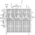
도 1은 본 발명의 일 실시예에 따른 곡면 표시 장치의 결합 사시도이고, 도 2는 도 1의 곡면 표시 장치의 분리 사시도이고, 도 3은 도 2의 표시 패널의 개략적인 레이아웃도이다.FIG. 1 is an assembled perspective view of a curved display device according to an embodiment of the present invention, FIG. 2 is an exploded perspective view of the curved display device of FIG. 1, and FIG. 3 is a schematic layout view of the display panel of FIG.
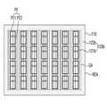
도 1 내지 도 3을 참조하면, 곡면 표시 장치(50)는 적어도 일부분에 곡률을 가지며, 상기 곡률과 대응하는 형상을 가지는 표시 패널(10), 백라이트 유닛(20), 중간 수납 용기(30) 및 상부 수납 용기(40)를 포함할 수 있다.1 to 3, the curved
표시 패널(10)은 영상을 표시하는 것으로, 상호 대향하는 제1 표시판(100) 및 제2 표시판(200)을 포함할 수 있다. 제1 표시판(100)과 제2 표시판(200)은 실링재(미도시)에 의해 결합할 수 있다. 제1 표시판(100)과 제2 표시판(200) 사이에는 액정층(도 5의 LC)이 개재될 수 있다.The
표시 패널(10)의 제1 표시판(100)과 제2 표시판(200) 각각은 화상이 표시되는 표시 영역(DA)과, 표시 영역(DA)의 적어도 일측에 위치하는 비표시 영역(NDA)을 포함한다. 표시 영역(DA)에는 매트릭스 형태로 배열되는 복수의 화소(PX)가 정의될 수 있다. 각 화소(PX)는 제1 전극(도 6의 PE)이 형성되는 화소 영역(도 6의 PA)과, 화소 영역(도 6의 PA) 이외의 영역인 비화소 영역(도 6의 NPA)을 포함할 수 있다. 비표시 영역(NDA)에는 게이트 패드(도 4의 GP) 및 데이터 패드(도 4의 DP)가 형성될 수 있다. 도 3에서는 비표시 영역(NDA)이 표시 영역(DA)을 감싸는 형태로 표시 패널(10)의 4개의 변에 대응되게 형성되는 것으로 도시되었으나, 4개 미만의 변에 대응되게 형성될 수도 있다.Each of the
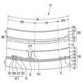
백라이트 유닛(20)은 표시 패널(10)에 광을 제공하는 것으로, 하부 수납 용기(21), 광원 모듈(22), 반사 시트(26), 광학 플레이트(27), 및 광학 시트(28)를 포함할 수 있다.The
하부 수납 용기(21)는 광원 모듈(22), 반사 시트(26), 광학 플레이트(27), 및 광학 시트(28) 등을 수납한다. 하부 수납 용기(21)는 바텀 샤시일 수 있다. 하부 수납 용기(21)는 광원 모듈(22)이 배치되는 함몰부(미도시)를 포함할 수 있다.The
광원 모듈(22)은 표시 패널(10)에 제공하는 광을 생성하는 복수의 광원(23), 예를 들어, LED(Light Emitting Diode) 광원과, 복수의 광원(23)을 구동시키는 전원을 제공하는 인쇄회로기판(24)과, 복수의 광원(23)으로부터 방출된 빛을 확산시키는 광학 렌즈(25)를 포함할 수 있다.The
반사 시트(26)는 하측을 향하는 광을 상측으로 반사시키는 역할을 한다. 반사 시트(26)는 전체가 하나로 연결될 수 있다. 반사 시트(26)는 광원(23)의 개수와 동수의 개구부(26a)를 포함할 수 있다.The
광학 플레이트(27)와 광학 시트(28)는 광원 모듈(22) 상부에 배치되어 광을 변조하는 광변조 구조물이다. 예시적인 실시예에서, 광학 플레이트(27)는 확산 플레이트일 수 있다. 광학 시트(28)로는 프리즘 시트, 확산 시트, 마이크로 렌즈 시트, 렌티큘러 시트, 위상차 보상 시트, 반사 편광 시트 등이 적용될 수 있다.The
중간 수납 용기(30)는 광학 시트(28)의 상부에 배치되며, 몰드 프레임 또는 미들 몰드일 수 있다. 중간 수납 용기(30)는 하부 수납 용기(21)에 체결되어 고정될 수 있다. 중간 수납 용기(30)는 표시 패널(10), 광학 플레이트(27) 및 광학 시트(28) 등을 수납할 수 있다.The
상부 수납 용기(40)는 표시 패널(10)의 상부에 배치되며, 탑 샤시 또는 베젤일 수 있다. 상부 수납 용기(40)는 개방창을 포함하며, 표시 패널(10)의 테두리를 덮어 보호한다. 상부 수납 용기(40)는 하부 수납 용기(21)와 결합할 수 있다.The
이하, 표시 패널(10)에 대해 더욱 상세히 설명한다. 표시 패널(10)의 구성에 대해서는 한 화소(PX)를 중심으로 설명한다.Hereinafter, the
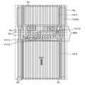
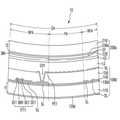
도 4는 도 2의 표시 패널을 설명하기 위한 세 개의 화소의 평면도이고, 도 5는 도 34의 표시 패널에서 I-I' 선의 단면도이다. 도 6은 도 2의 표시 패널의 제1 기판에서의 제1 편광층의 배치를 나타낸 레이아웃도이다. 도 7은 도 2의 패널의 제2 기판에서의 제2 편광층의 배치를 나타낸 레이아웃도이다.FIG. 4 is a plan view of three pixels for explaining the display panel of FIG. 2, and FIG. 5 is a sectional view of a line I-I 'in the display panel of FIG. 6 is a layout view showing the arrangement of the first polarizing layer in the first substrate of the display panel of Fig. 7 is a layout diagram showing the arrangement of the second polarizing layer in the second substrate of the panel of Fig.
도 4 및 도 5를 참조하면, 표시 패널(10)의 제1 표시판(100)은 제1 기판(110), 제1 편광층(120), 제1 절연층(130), 게이트 라인(GL), 데이터 라인(DL), 스토리지 라인(SL), 기준 라인(RL), 게이트 절연층(140), 제1 박막트랜지스터(TFT1), 제2 박막트랜지스터(TFT2), 제3 박막트랜지스터(TFT3), 보호층(150) 및 제1 전극(또는 화소 전극 이라함)(PE)을 포함한다.4 and 5, the
제1 기판(110)은 곡면 표시 장치(50)의 형상에 따라 적어도 일부분에 곡률을 가지며 표시 영역(DA)과, 비화소 영역(NDA)을 포함할 수 있다. 제1 기판(110)은 투과성, 내열성, 내화학성 등이 우수한 물질을 포함할 수 있다. 예를 들면, 제1 기판(110)은 광 투과력이 우수한 유리, 폴리에틸렌나프탈레이트, 폴리에틸렌테레프탈레이트층 및 폴리아크릴 중 어느 하나를 포함할 수 있다. 제1 기판(110)은 제1 두께(t1)를 가질 수 있다. 이러한 제1 기판(110)은 곡률을 가지는 백라이트 유닛(20)에 평평한 표시 패널(10)을 체결하여 곡면 표시 장치(50)를 제조하는 과정에서 제1 스트레스를 받을 수 있다.The
제1 편광층(120)은 제1 기판(110)과 액정층(LC) 사이에 형성된다. 예를 들어, 제1 편광층(120)은 제1 기판(110)과 박막트랜지스터들(TFT1, TFT2, TFT3) 사이에 형성될 수 있다. 즉, 제1 편광층(120)은 제1 기판(110) 상에 박막트랜지스터들(TFT1, TFT2, TFT3)를 포함하는 다른 구성들보다 먼저 형성되어, 제1 편광층(120)의 형성시 다른 구성들을 형성하기 위해 가해지는 고온에 의한 영향을 받지 않을 수 있다. 또한, 제1 편광층(120)은 제1 기판(110) 상에 직접 배치되어 제1 기판(110)의 평탄면에 용이하게 부착되거나, 제1 기판(110)의 평탄면에서 용이하게 제조될 수 있다. 도 6에서는, 제1 편광층(120)이 제1 기판(110) 상에 전면적으로 배치되는 것으로 도시되었으나, 이에 한정되는 것은 아니다. 몇몇 실시예에서, 제1 편광층(120)은 표시 영역(DA)과 대응되도록 배치될 수 있다.The first
제1 편광층(120)은 백라이트 유닛(20)으로부터 제공되는 내부광을 소정의 특정 방향으로 편광시킨다. 예를 들어, 제1 편광판(120)은 0°의 광축(도 6의 OA1)을 가지도록 형성되어, 상기 내부광을 0°로 편광시킨다. 제1 편광층(120)은 제1 기판(110)을 이미 통과한 내부광을 편광시킨다. 이에 따라, 제1 기판(110)에 광학적 이방성 현상이 발생되어 내부광의 위상 지연(retardation)이 발생하더라도, 제1 편광층(120)은 이미 위상 지연이 발생된 내부광을 편광시키므로 편광 특성이 유지된 광이 액정층(LC)에 제공될 수 있다. 제1 기판(110)의 광학적 이방성 현상은 곡률을 가지는 백라이트 유닛(20)에 평평한 표시 패널(10)을 체결하여 곡면 표시 장치(50)를 제조하는 과정에서 제1 기판(110)에 발생되는 제1 스트레스에 의해 발생될 수 있다.The first
한편, 제1 편광층(120)이 제1 기판(110)의 외부에 배치되면, 액정층(LC)에 제공되는 광의 편광 특성은 제1 편광층(120)에 의해 편광된 내부광의 편광 특성과 다를 수 있다. 이는 제1 편광판(120)에 의해 편광된 내부광이 광학적 이방성을 가지는 제1 기판(110)을 통과하면서, 제1 편광판(120)에 의해 편광된 내부광에 위상 지연이 발생될 수 있기 때문이다.When the first
제1 편광층(120)은 상기 특정 방향으로 편광시키는 광 이외의 광을 흡수시키는 흡수형 편광층이거나, 상기 특정 방향으로 편광시키는 광 이외의 광을 반사시키는 반사형 편광층일 수 있다. 상기 흡수형 편광층은 연신한 폴리비닐알코올 필름에 요오드 또는 이색성 염료를 염착시킴으로 형성될 수 있다. 상기 반사형 편광층은 전도성 물질을 패터닝함으로써 형성될 수 있으며, 와이어 그리드 편광 패턴으로 형성될 수 있다. 도 5 및 도 6에서는, 제1 편광층(120)이 흡수형 편광층으로 구현된 경우를 도시하였다.The first
제1 절연층(130)은 제1 편광층(120) 상에 배치된다. 제1 절연층(130)은 제1 편광층(120)을 평탄화하면서 보호하는 역할을 할 수 있다. 제1 절연층(130)은 실리콘 산화물(SiOx)을 포함할 수 있다. 제1 절연층(130)은 생략될 수도 있다.The first insulating
게이트 라인(GL)은 제1 기판(110), 구체적으로 제1 절연층(130) 상에 제1 방향으로 연장되게 형성되며, 게이트 신호를 전달한다. 게이트 라인(GL)의 일단에는 게이트 패드(GP)가 연결된다. 게이트 패드(GP) 상에는 게이트 패드 전극(GPE)이 형성될 수 있다. 게이트 패드 전극(GPE)은 제1 전극(PE)에 신호를 인가하기 위한 외부 배선을 연결하기 위한 컨택 전극이다.The gate line GL is formed to extend in the first direction on the
데이터 라인(DL)은 제1 기판(110), 구체적으로 게이트 절연층(140) 상에 상기 제1 방향과 교차하는 제2 방향으로 연장되게 형성되며, 게이트 라인(GL)과 절연되고 데이터 신호를 전달한다. 데이터 라인(DL)의 일단에는 데이터 패드(DP)가 연결된다. 데이터 패드(DP) 상에는 데이터 패드 전극(DPE)이 형성될 수 있다. 데이터 패드 전극(DPE)은 제1 전극(PE)에 신호를 인가하기 위한 외부 배선을 연결하기 위한 또 하나의 컨택 전극이다.The data line DL is formed to extend in the second direction intersecting the first direction on the
스토리지 라인(SL)은 제1 기판(110), 구체적으로 제1 절연층(130) 상에 상기 제1 방향으로 연장되며, 상기 제2 방향으로 분기되어 제1 전극(PE; PE1, PE2)을 둘러싸는 분기 전극들을 더 포함한다. 스토리지 라인(SL)은 제1 전극(PE) 사이에 유지 커패시터를 형성하여, 제1 전극(PE)과 제2 전극(CE) 사이에 형성되는 액정 커패시터의 전압 유지 능력을 강화시킬 수 있다.The storage line SL extends in the first direction on the
게이트 절연층(140)은 제1 절연층(130) 상에 형성되는 게이트 라인(GL), 스토리지 라인(SL) 및 게이트 패드(GP)를 커버하고, 절연 물질로 형성된다. 예를 들어, 게이트 절연층(140)은 실리콘 질화물(SiNx) 또는 실리콘 산화물(SiOx)등의 무기 물질을 포함할 수 있다.The
제1 박막트랜지스터(TFT1)는 제1 편광층(120)과 액정층(LC) 사이에 배치되며 게이트 라인(GL)과 데이터 라인(DL) 사이에 연결되고, 제1 게이트 전극(GE1), 제1 반도체층(SM1), 제1 소스 전극(SE1) 및 제1 드레인 전극(DE1)을 포함한다.The first thin film transistor TFT1 is disposed between the first
제1 게이트 전극(GE1)은 평면상으로 게이트 라인(GL)으로부터 제1 반도체층(SM1) 측으로 돌출되어 형성될 수 있다. 제1 게이트 전극(GE1)은 인듐틴옥사이드(ITO), 인듐징크옥사이드(IZO), 인듐틴징크옥사이드(ITZO) 중 어느 하나를 포함할 수 있다. 또한, 제1 게이트 전극(GE1)은 상술한 물질로 구성된 제1 전극층과 후술하는 물질로 구성된 제2 전극층을 포함하는 2층 구조를 가질 수도 있다. 상기 제2 전극층은 구리(Cu), 몰리브덴(Mo), 알루미늄(Al), 텅스텐(W), 크롬(Cr), 티타늄(Ti)과 같은 금속이나, 적어도 하나의 상기 금속을 포함하는 합금일 수 있다.The first gate electrode GE1 may protrude from the gate line GL toward the first semiconductor layer SM1 side in a plan view. The first gate electrode GE1 may include any one of indium tin oxide (ITO), indium zinc oxide (IZO), and indium tin zinc oxide (ITZO). Further, the first gate electrode GE1 may have a two-layer structure including a first electrode layer composed of the above-described material and a second electrode layer composed of a material described later. The second electrode layer may be a metal such as copper (Cu), molybdenum (Mo), aluminum (Al), tungsten (W), chromium (Cr), titanium (Ti), or an alloy containing at least one of the metals have.
제1 반도체층(SM1)은 게이트 절연층(140)을 사이에 두고 제1 게이트 전극(GE1) 상에 형성된다. 제1 반도체층(SM1)은 제1 게이트 절연층(140) 상에 제공되는 활성층과 상기 활성층 상에 제공되는 오믹 컨택층을 포함할 수 있다. 한편, 제1 반도체층(SM1)은 데이터 라인(DL)과 게이트 절연층(140) 사이에 형성될 수 있다. 또한, 제1 반도체층(SM1)은 데이터 패드(DP)와 게이트 절연층(140) 사이에도 형성될 수 있다.The first semiconductor layer SM1 is formed on the first gate electrode GE1 with the
제1 소스 전극(SE1)은 데이터 라인(DL)에서 돌출되어 형성되며, 평면상으로 제1 게이트 전극(GE)의 적어도 일부와 중첩한다. 제1 드레인 전극(DE1)은 제1 소스 전극(SE1)으로부터 이격되게 형성되며, 평면상으로 제1 게이트 전극(GE1)의 적어도 일부와 중첩한다. 제1 드레인 전극(DE1)은 보호층(150)에 형성되는 제1 컨택홀(CH1)을 통해 제1 전극(PE)의 제1 서브 전극(PE1)과 연결된다. 제1 소스 전극(SE1)과 제1 드레인 전극(DE1)은 구리, 몰리브덴, 알루미늄, 텅스텐, 크롬, 티타늄과 같은 금속이나, 적어도 하나의 상기 금속을 포함하는 합금일 수 있다. 여기서, 제1 소스 전극(SE1)과 제1 드레인 전극(DE1)은 제1 소스 전극(SE1)과 제1 드레인 전극(DE1) 사이의 이격된 영역을 제외한 영역에서 제1 반도체층(SM1)의 일부와 중첩한다.The first source electrode SE1 protrudes from the data line DL and overlaps at least part of the first gate electrode GE in a plane. The first drain electrode DE1 is formed so as to be spaced apart from the first source electrode SE1 and overlaps at least part of the first gate electrode GE1 in a plan view. The first drain electrode DE1 is connected to the first sub electrode PE1 of the first electrode PE through the first contact hole CH1 formed in the
제2 박막트랜지스터(TFT2)는 제1 편광층(120)과 액정층(LC) 사이에 배치되며 게이트 라인(GL)과 데이터 라인(DL) 사이에 연결되고, 제2 게이트 전극(GE2), 제2 반도체층(SM2), 제2 소스 전극(SE2) 및 제2 드레인 전극(DE2)을 포함한다.The second thin film transistor TFT2 is disposed between the first
제2 게이트 전극(GE2)은 평면상으로 게이트 라인(GL)으로부터 제2 반도체층(SM2) 측으로 돌출되어 형성되며, 제1 게이트 전극(GE1)과 연결된다. 제2 게이트 전극(GE2)은 제1 게이트 전극(GE1)과 동일한 물질로 형성될 수 있다.The second gate electrode GE2 protrudes from the gate line GL toward the second semiconductor layer SM2 in a plan view and is connected to the first gate electrode GE1. The second gate electrode GE2 may be formed of the same material as the first gate electrode GE1.
제2 반도체층(SM2)은 게이트 절연층(140)을 사이에 두고 제2 게이트 전극(GE2) 상에 형성된다. 제2 반도체층(SM2)은 게이트 절연층(140) 상에 제공되는 활성층과 상기 활성층 상에 제공되는 오믹 컨택층을 포함할 수 있다. 한편, 제2 반도체층(SM2)은 데이터 라인(DL)과 게이트 절연층(140) 사이에 형성될 수 있다. 또한, 제2 반도체층(SM2)은 데이터 패드(DP)와 게이트 절연층(140) 사이에도 형성될 수 있다.The second semiconductor layer SM2 is formed on the second gate electrode GE2 with the
제2 소스 전극(SE2)은 제1 소스 전극(SE1)과 연결되며, 평면상으로 제2 게이트 전극(GE2)의 적어도 일부와 중첩한다. 제2 드레인 전극(DE2)은 제2 소스 전극(SE2)으로부터 이격되게 형성되며, 평면상으로 제2 게이트 전극(GE2)의 적어도 일부와 중첩한다. 제2 드레인 전극(DE2)은 보호층(150)에 형성되는 제2 컨택홀(CH2)을 통해 제1 전극(PE)의 제2 서브 전극(PE2)과 연결된다. 여기서, 제2 소스 전극(SE2)과 제2 드레인 전극(DE2)은 제2 소스 전극(SE2)과 제2 드레인 전극(DE2) 사이의 이격된 영역을 제외한 영역에서 제2 반도체층(SM2)의 일부와 중첩한다. 제2 소스 전극(SE2) 및 제2 드레인 전극(DE2)은 제1 소스 전극(SE1) 및 제1 드레인 전극(DE1)과 동일한 물질로 형성될 수 있다.The second source electrode SE2 is connected to the first source electrode SE1 and overlaps at least part of the second gate electrode GE2 in a plane. The second drain electrode DE2 is formed apart from the second source electrode SE2 and overlaps with at least part of the second gate electrode GE2 in a plane. The second drain electrode DE2 is connected to the second sub electrode PE2 of the first electrode PE through the second contact hole CH2 formed in the
제3 박막트랜지스터(TFT3)는 제1 편광층(120)과 액정층(LC) 사이에 배치되며 게이트 라인(GL)과 데이터 라인(DL) 사이에 연결되고, 제3 게이트 전극(GE3), 제3 반도체층(SM3), 제3 소스 전극(SE3) 및 제3 드레인 전극(DE3)을 포함한다.The third thin film transistor TFT3 is disposed between the first
제3 게이트 전극(GE3)은 평면상으로 게이트 라인(GL)으로부터 제3 반도체층(SM3) 측으로 돌출되어 형성되며, 제2 게이트 전극(GE2)과 이격된다. 제3 게이트 전극(GE3)은 제1 게이트 전극(GE1)과 동일한 물질로 형성될 수 있다.The third gate electrode GE3 protrudes from the gate line GL toward the third semiconductor layer SM3 in a plan view, and is separated from the second gate electrode GE2. The third gate electrode GE3 may be formed of the same material as the first gate electrode GE1.
제3 반도체층(SM3)은 게이트 절연층(140)을 사이에 두고 제3 게이트 전극(GE3) 상에 형성된다. 제3 반도체층(SM3)은 게이트 절연층(140) 상에 제공되는 활성층과 상기 활성층 상에 제공되는 오믹 컨택층을 포함할 수 있다. 한편, 제3 반도체층(SM3)은 데이터 라인(DL)과 게이트 절연층(140) 사이에 형성될 수 있다. 또한, 제3 반도체층(SM3)은 데이터 패드(DP)와 게이트 절연층(140) 사이에도 형성될 수 있다.The third semiconductor layer SM3 is formed on the third gate electrode GE3 with the
제3 소스 전극(SE3)은 제2 드레인 전극(DE2)과 연결되며, 평면상으로 제3 게이트 전극(GE3)의 적어도 일부와 중첩한다. 제3 드레인 전극(DE3)은 제3 소스 전극(SE3)으로부터 이격되게 형성되며, 평면상으로 제3 게이트 전극(GE3)의 적어도 일부와 중첩한다. 제3 드레인 전극(DE3)은 보호층(150)에 형성되는 제3 컨택홀(CH3)을 통해 후술하는 기준 라인(RL)과 연결된다. 여기서, 제3 소스 전극(SE3)과 제3 드레인 전극(DE3)은 제3 소스 전극(SE3)과 제3 드레인 전극(DE3) 사이의 이격된 영역을 제외한 영역에서 제3 반도체층(SM3)의 일부와 중첩한다. 제3 소스 전극(SE3) 및 제3 드레인 전극(DE3)는 제1 소스 전극(SE1) 및 제1 드레인 전극(DE1)과 동일한 물질로 형성될 수 있다.The third source electrode SE3 is connected to the second drain electrode DE2 and overlaps at least part of the third gate electrode GE3 in a plan view. The third drain electrode DE3 is formed apart from the third source electrode SE3 and overlaps with at least a part of the third gate electrode GE3 in a plane. The third drain electrode DE3 is connected to a reference line RL described later through a third contact hole CH3 formed in the
보호층(150)은 제1 박막트랜지스터(TFT1), 제2 박막트랜지스터(TFT2) 및 제3 박막트랜지스터(TFT3) 상에 배치된다. 보호층(150)은 실리콘 질화물(SiNx) 또는 실리콘 산화물(SiOx)등의 무기 물질로 형성될 수도 있고, 저유전율 유기 절연막으로 형성될 수도 있다. 또한, 보호층(150)은 무기 절연막과 유기 절연막의 이중막으로 형성될 수도 있다. 보호층(150)은 제1 드레인 전극(DE1)의 일부를 노출하는 제1 컨택홀(CH1)과, 제2 드레인 전극(DE2)의 일부를 노출하는 제2 컨택홀(CH2)과, 제3 드레인 전극(DE3)의 일부를 노출하는 컨택홀(CH3)을 갖는다.The
제1 전극(PE)은 제1 편광층(120)과 액정층(LC) 사이, 구체적으로 보호층(150) 상에 각 화소(도 3의 PX) 단위로 배치되며, 평면상으로 박막트랜지스터들(TFT1, TFT2, TFT3)을 사이에 두고 배치되는 제1 서브 전극(PE1)과 제2 서브 전극(PE2)을 포함할 수 있다.The first electrode PE is arranged in units of pixels (PX in FIG. 3) between the first
제1 서브 전극(PE1)은 제1 컨택홀(CH1)을 통해 제1 드레인 전극(DE1)에 접촉한다. 제1 서브 전극(PE1)은 복수의 개구를 갖는 슬릿 패턴을 포함할 수 있다. 예를 들어, 제1 서브 전극(PE1)은 줄기부(PE1a)와, 줄기부(PE1a)로부터 돌출되어 연장된 복수의 가지부들(PE1b)과, 줄기 전극(PE1a)과 제1 드레인 전극(DE1)을 연결하는 연결 전극(PE1c)을 포함할 수 있다. 줄기부(PE1a)는 하나의 수평 라인과 세개의 수직 라인을 포함하는 형태로 형성될 수 있다. 상기 하나의 수직 라인은 하나의 수평 라인과 교차할 수 있으며, 두 개의 수직 라인은 하나의 수평 라인의 양측에 연결될 수 있다. 가지부들(PE1b)은 스토리지 라인(SL)이 형성된 영역에까지 연장되어 형성될 수 있다. 줄기부(PE1a)와 복수의 가지부들(PE1b)은 도 4에 도시된 배열 형태로 한정되는 것은 아니며, 다양한 배열 형태를 가질 수 있다. 제1 서브 전극(PE1)은 투명 도전 물질을 포함할 수 있다. 예를 들면, 제1 서브 전극(PE1)은 산화 인듐 주석(indium tin oxide: ITO) 또는 산화 아연 주석(indium zinc oxide: IZO)를 포함할 수 있다. 제1 서브 전극(PE1)은 스토리지 라인(SL)과 부분적으로 오버랩되어 스토리지 커패시터를 형성할 수 있다.The first sub-electrode PE1 contacts the first drain electrode DE1 through the first contact hole CH1. The first sub-electrode PE1 may include a slit pattern having a plurality of openings. For example, the first sub-electrode PE1 includes a stripe portion PE1a, a plurality of branch portions PE1b protruding from the stripe portion PE1a, a stem electrode PE1a and a first drain electrode DE1 And a connecting electrode PE1c connecting the electrodes. The stripe portion PE1a may be formed to include one horizontal line and three vertical lines. The one vertical line may intersect one horizontal line, and the two vertical lines may be connected to both sides of one horizontal line. The branches PE1b may extend to a region where the storage line SL is formed. The stem portion PE1a and the plurality of branch portions PE1b are not limited to the arrangement shown in FIG. 4, and may have various arrangements. The first sub-electrode PE1 may include a transparent conductive material. For example, the first sub-electrode PE1 may include indium tin oxide (ITO) or indium zinc oxide (IZO). The first sub-electrode PE1 partially overlaps with the storage line SL to form a storage capacitor.
제2 서브 전극(PE2)은 제2 컨택홀(CH2)을 통해 제2 드레인 전극(DE2)에 접촉한다. 제2 서브 전극(PE2)은 복수의 개구를 갖는 슬릿 패턴을 포함할 수 있다. 예를 들어, 제2 서브 전극(PE2)은 줄기부(PE2a)와, 줄기부(PE2a)로부터 돌출되어 연장된 복수의 가지부들(PE2b)과, 줄기 전극(PE2a)과 제2 드레인 전극(DE2)을 연결하는 연결 전극(PE2c)을 포함할 수 있다. 줄기부(PE2a)는 하나의 수평 라인과 세개의 수직 라인을 포함하는 형태로 형성될 수 있다. 가지부들(PE2b)은 스토리지 라인(SL)이 형성된 영역에까지 연장되어 형성될 수 있다. 줄기부(PE2a)와 복수의 가지부들(PE2b)은 도 4에 도시된 배열 형태로 한정되는 것은 아니며, 다양한 배열 형태를 가질 수 있다. 제2 서브 전극(PE2)는 제1 서브 전극(PE1)과 동일한 물질로 형성될 수 있다. 제2 서브 전극(PE2)은 스토리지 라인(SL)과 부분적으로 오버랩되어 스토리지 커패시터를 형성할 수 있다. 한편, 제1 서브 전극(PE1)이 배치된 제1 서브 화소와 제2 서브 전극(PE2)이 배치된 제2 서브 화소의 크기는 상이할 수 있다. 예를 들어, 제2 서브 화소의 크기가 제1 서브 화소의 크기보다 클 수 있다.And the second sub-electrode PE2 contacts the second drain electrode DE2 through the second contact hole CH2. The second sub-electrode PE2 may include a slit pattern having a plurality of openings. For example, the second sub-electrode PE2 includes a stripe portion PE2a, a plurality of branch portions PE2b protruding from the stripe portion PE2a, a stem electrode PE2a and a second drain electrode DE2 And a connecting electrode PE2c connecting the electrodes. The stripe portion PE2a may be formed in a shape including one horizontal line and three vertical lines. The branches PE2b may extend to a region where the storage line SL is formed. The stem portion PE2a and the plurality of branch portions PE2b are not limited to the arrangement shown in FIG. 4, and may have various arrangements. The second sub-electrode PE2 may be formed of the same material as the first sub-electrode PE1. The second sub-electrode PE2 may partly overlap with the storage line SL to form a storage capacitor. On the other hand, the sizes of the first and second sub-pixels including the first sub-electrode PE1 and the second sub-electrode PE2 may be different. For example, the size of the second sub-pixel may be greater than the size of the first sub-pixel.
기준 라인(RL)은 보호층(150) 상에 배치된다. 기준 라인(RL)은 상기 제2 방향으로 연장되고, 평면상에서 데이터 라인(DL)의 일부와 중첩되며 제3 박막트랜지스터(TFT3)의 일부와 중첩하도록 돌출된 돌출부를 포함하도록 형성된다. 기준 라인(RL)의 돌출부는 제3 컨택홀(CH3)을 통해 제3 박막트랜지스터(TFT3)의 제3 드레인 전극(DE3)과 접촉한다. 또한, 기준 라인(RL)은 제1 서브 화소(PE1)와 제2 서브 화소(PE2) 사이의 이격된 영역에 연장되게 형성될 수 있다. 기준 라인(RL)은 제1 서브 전극(PE1) 및 제2 서브 전극(PE2)과 동일한 층에 동일한 물질로 형성될 수 있다.The reference line RL is disposed on the
기준 라인(RL)에는 스토리지 라인(RL)과 동일한 레벨의 기준 전압이 인가될 수 있다. 이러한 기준 라인(RL)은 제3 박막트랜지스터(TFT3)를 통해 제2 서브 전극(PE2)에 인가되는 전압을 낮춰, 제2 서브 전극(PE2)과 제2 전극(CE) 사이의 전압이 제1 서브 전극(PE1)과 제2 전극(CE) 사이의 전압보다 낮은 크기를 가지게 할 수 있다. 이로 인해, 제1 서브 전극(PE1)이 위치하는 제1 서브 화소에 대응하는 영역에 위치하는 액정 분자들과 제2 서브 전극(PE2)이 위치하는 제2 서브 화소에 대응하는 영역에 위치하는 액정 분자들이 서로 다른 전기장 세기를 받아 서로 다른 각도로 기울어지게 된다. 이에 따라, 상기 제1 서브 화소에 대응하는 영역에 위치하는 액정 분자들과 상기 제2 서브 화소에 대응하는 영역에 위치하는 액정 분자들이 서로 다른 경사각을 가지게 되어, 상기 제1 서브 화소의 휘도와 상기 제2 서브 화소의 휘도가 달라진다. 이에 따라, 측면 시인성이 향상될 수 있다. 한편, 기준 라인(RL)은 데이터 라인(DL)과 제1 전극(PE) 사이, 데이터 라인(DL)과 제2 전극(CE) 사이의 전자기 간섭을 차단하는 차폐 전극으로 작용할 수도 있다.A reference voltage of the same level as the storage line RL may be applied to the reference line RL. The reference line RL lowers the voltage applied to the second sub-electrode PE2 through the third thin film transistor TFT3 and the voltage between the second sub-electrode PE2 and the second electrode CE becomes lower than the first The voltage between the sub electrode PE1 and the second electrode CE can be lower than the voltage between the sub electrode PE1 and the second electrode CE. Therefore, the liquid crystal molecules located in the region corresponding to the first sub-pixel where the first sub-electrode PE1 is located and the liquid crystal molecules located in the region corresponding to the second sub- The molecules are tilted at different angles with different electric field strengths. Accordingly, the liquid crystal molecules located in the region corresponding to the first sub-pixel and the liquid crystal molecules located in the region corresponding to the second sub-pixel have different inclination angles, and the brightness of the first sub- The luminance of the second sub-pixel is changed. Thus, side viewability can be improved. On the other hand, the reference line RL may serve as a shielding electrode which shields electromagnetic interference between the data line DL and the first electrode PE, and between the data line DL and the second electrode CE.
제2 표시판(200)은 제2 기판(210), 블랙 매트릭스(BM), 컬러 필터(CF), 오버 코팅층(220), 제2 전극(CE) 및 제2 편광층(230)을 포함한다.The
제2 기판(210)은 곡면 표시 장치(50)의 형상과 대응되도록 적어도 일부분에 곡률을 가지며, 제1 기판(110)과 대향한다. 제2 기판(110)은 투과성, 내열성, 내화학성 등이 우수한 물질을 포함할 수 있다. 예를 들면, 제1 기판(110)은 광 투과력이 우수한 유리, 폴리에틸렌나프탈레이트, 폴리에틸렌테레프탈레이트층 및 폴리아크릴 중 어느 하나를 포함할 수 있다. 제2 기판(210)은 제1 기판(110)의 제1 두께(t1)와 같은 제2 두께(t2)를 가질 수 있다. 이러한 제2 기판(210)은 곡률을 가지는 백라이트 유닛(20)에 평평한 표시 패널(10)을 체결하여 곡면 표시 장치(50)를 제조하는 과정에서 제1 기판(110)의 제 1 스트레스와 같은 제2 스트레스를 받을 수 있다.The
블랙 매트릭스(BM)는 제2 기판(210)의 하부에 배치된다. 구체적으로, 블랙 매트릭스(BM)는 비화소 영역(NPA)의 적어도 일부 영역에 대응되어 배치된다. 예를 들어, 블랙 매트릭스(BM)는 게이트 라인(GL) 및 박막 트랜지스터들(TFT1, TFT2, TFT3)과 중첩할 수 있다. 이 경우, 곡면 표시 장치의 구현을 위해 표시 패널을 데이터 라인과 평행한 방향을 축으로 휘는 경우에 있어서 제1 표시판과 제2 표시판이 미스 얼라인 되면서 데이터 라인과 중첩하는 블랙 매트릭스가 제1 전극이 형성된 부분으로 침범하여 실질적으로 화상이 표시되는 영역(제1 전극 부분)이 줄어드는 것이 방지될 수 있다. 또한, 블랙 매트릭스(BM)는 비표시 영역(NDA)에 대응되어 배치된다. 이러한 블랙 매트릭스(BM)은 불필요한 광을 차단한다. 몇몇 실시예에서, 블랙 매트릭스(BM)는 제1 기판(110) 상에 형성될 수 있다. 이 때, 블랙 매트릭스(BM)는 게이트 라인(GL), 데이터 라인(DL) 및 박막 트랜지스터들(TFT1, TFT2, TFT3)과 중첩할 수 있다. 이 경우, 곡면 표시 장치의 구현을 위해 표시 패널을 데이터 라인과 평행한 방향을 축으로 휘는 경우에 있어서 제1 표시판과 제2 표시판이 미스 얼라인되더라도 블랙 매트릭스와 제1 전극 모두가 제1 기판 상에 위치하므로 데이터 라인과 중첩하는 블랙 매트릭스가 제1 전극이 형성된 부분으로 침범하지 않는다. 이에 따라, 실질적으로 화상이 표시되는 영역이 줄어드는 것이 방지될 수 있다.The black matrix BM is disposed below the
컬러 필터(CF)는 블랙 매트릭스(BM)가 배치된 제2 기판(210)의 하부에 배치된다. 컬러 필터(CF)는 액정층(LC)을 투과하는 광에 색을 제공하기 위한 것이다. 컬러 필터(CF)는 적색 컬러 필터(red), 녹색 컬러 필터(green), 및 청색 컬러 필터(blue)일 수 있다. 컬러 필터(CF)는 각 화소 영역(PA)에 대응하여 제공되며, 서로 인접한 화소들(PX) 사이에서 서로 다른 색을 갖도록 배치될 수 있다. 컬러 필터(CF)는 서로 인접한 화소들(PX)의 경계에서 일부가 인접하게 중첩되거나, 또는 서로 인접한 화소들(PX)의 경계에서 이격될 수 있다. 몇몇 실시예에서, 컬러 필터(CF)는 제1 기판(110) 상에 형성될 수 있다.The color filter CF is disposed below the
오버 코팅층(220)은 컬러 필터(CF) 및 블랙 매트릭스(BM)의 하부에 형성된다. 오버 코팅층(220)은 컬러 필터(CF)를 평탄화하면서 컬러 필터(CF)를 보호하는 역할과 절연하는 역할을 하며, 아크릴계 에폭시 재료를 이용하여 형성될 수 있다.The
제2 전극(CE)은 오버 코팅층(220) 및 액정층(LC) 사이에 배치되며, 오버 코팅층(220) 상에 전면적으로 형성될 수 있다. 제2 전극(CE)은 공통 라인(미도시)과 전기적으로 연결된다. 제2 전극(CE)은 투명 도전 물질을 포함할 수 있다. 예를 들면, 제2 전극(CE)은 산화 인듐 주석(indium tin oxide: ITO) 또는 산화 아연 주석(indium zinc oxide: IZO)를 포함할 수 있다.The second electrode CE is disposed between the
제2 편광층(230)은 제2 기판(210)의 외측에 배치되며, 제2 기판(210) 상에 전면적으로 형성될 수 있다. 제2 편광층(230)은 액정층(LC)을 통과한 광을 상기 특정 방향과 수직인 방향으로 편광시킨다. 예를 들어, 도 7에 도시된 바와 같이 제2 편광판(230)은 제1 편광판(120)의 0°의 광축(도 6의 OA1)과 직교하는 90°의 광축(OA2)을 가지도록 형성되어, 액정층(LC)을 통과한 광을 90°로 편광시킨다. 한편, 곡면 표시 장치(50)가 블랙 영상을 표시하도록 액정층(LC)의 액정 분자들의 배열이 제어된 경우, 액정층(LC)을 통과한 광이 제2 편광층(230)에 통과되지 말아야 한다. 그런데, 액정층(LC)을 통과한 광이 광학적 이방성 현상이 발생되는 제2 기판(210)을 통과하는 경우, 액정층(LC)을 통과한 광에 위상 지연이 발생될 수 있다. 이러한 위상 지연이 발생된 광이 제2 편광층(230)에 제공되는 경우, 위상 지연이 발생된 광의 일부가 제2 편광층(230)을 통과하여 블랙 영상에 미미한 빛샘 현상이 발생될 수 있다. 상기 미미한 빛샘 현상은 크게 인식되지는 않는다. 제2 기판(230)의 광학적 이방성 현상은 곡률을 가지는 백라이트 유닛(20)에 평평한 표시 패널(10)을 체결하여 곡면 표시 장치(50)를 제조하는 과정에서 제2 기판(230)에 발생되는 제2 스트레스에 의해 발생될 수 있다.The second
제2 편광층(230)은 상기 특정 방향과 수직인 방향으로 편광시키는 광 이외의 광을 흡수시키는 흡수형 편광층이거나, 상기 특정 방향과 수직인 방향으로 편광시키는 광 이외의 광을 반사시키는 반사형 편광층일 수 있다.The second
도 5 및 도 7에서, 제2 편광층(230)은 흡수형 편광층으로 형성된 것이 도시되었다. 제2 편광층(230)이 흡수형 편광층으로 형성된 경우, 제2 편광층(230)으로 입사되는 외부광이 제2 편광층(230)으로부터 반사됨으로 인해 발생되는 눈부심 현상이 줄어들 수 있다. 한편, 도 7에서 제2 편광층(230)이 제2 기판(210) 상에 전면적으로 배치되는 것으로 도시되었으나, 이에 한정되는 것은 아니다. 몇몇 실시예에서, 제2 편광층(230)은 표시 영역(DA)과 대응되도록 배치될 수 있다.5 and 7, the second
표시 패널(10)의 액정층(LC)은 유전율 이방성을 가지는 액정 분자를 포함한다. 상기 액정 분자는 전기장이 없는 상태에서 그 장축이 두 표시판(100, 200)의 표면에 대하여 수직 또는 수평을 이룰 수 있다.The liquid crystal layer LC of the
상기와 같은 구조를 가지는 곡면 표시 장치(50)에서 게이트 라인(GL)을 통해 게이트 신호가 제공되고 데이터 라인(DL)을 통해 제1 박막트랜지스(TFT1) 및 제2 박막트랜지스터(TFT2)를 통해 데이터 신호가 제공된다. 그럼, 제1 박막트랜지스(TFT1) 및 제2 박막트랜지스터(TF2T)가 턴온되어 데이터 신호에 해당하는 전압이 제1 서브 전극(PE1)과 제2 서브 전극(PE2)에 제공된다. 이 때, 제2 서브 전극(PE2)에 인가되는 전압은 기준 전압이 인가되는 기준 라인(RL)과 연결되는 제3 박막트랜지스터(TFT3)의 턴온에 의해 분압되어 제1 서브 전극(PE1)에 인가되는 전압보다 낮을 수 있다. 서로 다른 전압이 인가되는 제1 서브 전극(PE1)과 제2 서브 전극(PE2) 각각과 공통 전압이 인가되는 제2 전극(CE) 사이에는 서로 다른 크기의 전계가 형성된다. 서로 다른 전계에 따라, 제1 서브 전극(PE1)과 제2 전극(CE) 사이에 위치하는 액정 분자와 제2 서브 전극(PE2)과 제2 전극(CE) 사이에 위치하는 액정 분자가 구동되며 그 결과 액정층(LC)을 투과하는 광량에 따라 화상이 표시된다.In a
상기와 같이 본 발명의 일 실시예에 따른 곡면 표시 장치(50)는 제1 기판(110)과 액정층(LC) 사이에 형성되는 제1 편광층(120)을 구비함으로써, 제1 기판(110)에 광학적 이방성 현상이 발생하더라도 제1 편광층(120)의 편광 특성이 유지된 광을 액정층(LC)에 제공하게 할 수 있다.As described above, the
따라서, 본 발명의 일 실시예에 따른 곡면 표시 장치(50)는 제1 편광층이 제1 기판의 외부에 배치되는 경우 제1 기판의 광학적 이방성 현상으로 인해 제1 편광층에 의해 편광된 광에 위상 지연이 발생된 광(제1 편광층의 편광 특성과 다른 편광 특성을 가지는 광)이 액정층을 통과함으로써 원하지 않는 영상이 표시되게 하는 것, 예를 들어 블랙 영상에 빛샘 현상이 발생되게 하는 것을 줄일 수 있다.Therefore, the curved
다음은 본 발명의 다른 실시예에 따른 곡면 표시 장치에 대해 설명하기로 한다.Next, a curved display device according to another embodiment of the present invention will be described.
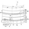
도 8은 본 발명의 다른 실시예에 따른 곡면 표시 장치 중 도 5의 표시 패널과 대응되는 표시 패널의 단면도이고, 도 9는 도 8의 표시 패널을 설명하기 위한 한 화소의 평면도이고, 도 10은 도 8의 표시 패널의 제1 기판에서의 제1 편광층의 배치를 나타낸 레이아웃도이고, 도 11 및 도 12는 도 10의 제1 편광층의 다양한 실시예를 나타내는 레이아웃도들이다. 도 9에서는 제1 서브 전극(PE1) 및 제2 서브 전극(PE2)이 점선으로 표시된 사각형 영역에 형성되며, 제1 서브 전극(PE1) 및 제2 서브 전극(PE2)의 구체적인 형상은 생략되었다.8 is a cross-sectional view of a display panel corresponding to the display panel of FIG. 5 of a curved surface display device according to another embodiment of the present invention, FIG. 9 is a plan view of a pixel for explaining the display panel of FIG. 8, 8 is a layout diagram showing the arrangement of the first polarizing layer in the first substrate of the display panel in Fig. 8, and Figs. 11 and 12 are layout diagrams showing various embodiments of the first polarizing layer in Fig. In FIG. 9, the first sub-electrode PE1 and the second sub-electrode PE2 are formed in a rectangular area indicated by a dotted line, and the specific shapes of the first sub-electrode PE1 and the second sub-electrode PE2 are omitted.
도 8을 참조하면, 본 발명의 다른 실시예에 따른 곡면 표시 장치는 도 2의 곡면 표시 장치(50)와 비교하여 표시 패널(11)만 다르며 동일한 구성을 가진다. 이에 따라, 본 발명의 다른 실시예에 따른 곡면 표시 장치에서는 표시 패널(11)에 대해서만 설명하기로 한다.Referring to FIG. 8, the curved surface display device according to another embodiment of the present invention is different from the curved
표시 패널(11)은 상호 대향하는 제1 표시판(100a) 및 제2 표시판(200)을 포함할 수 있다. 제1 표시판(100a)과 제2 표시판(200)은 실링재(미도시)에 의해 결합할 수 있다. 제1 표시판(100a)과 제2 표시판(200) 사이에는 액정층(LC)이 개재될 수 있다.The
표시 패널(11)의 제1 표시판(100a)은 제1 기판(110), 제1 편광층(120a), 제1 절연층(130a), 게이트 라인(GL), 데이터 라인(DL), 스토리지 라인(SL), 기준 라인(RL), 게이트 절연층(140), 제1 박막트랜지스터(TFT1), 제2 박막트랜지스터(TFT2), 제3 박막트랜지스터(TFT3), 보호층(150) 및 제1 전극(PE)을 포함하며, 도 5의 제1 표시판(100)과 유사하다.The
다만, 제1 편광층(120a)이 반사형 편광층으로 형성된다. 이 경우, 제1 편광층(120a)은 복수의 금속선으로 구성된다. 상기 복수의 금속선(121)은 패터닝 방법 등을 통해 제1 기판(110) 상에 일 방향으로 연장되며 상기 일방향과 수직인 방향으로 서로 일정 간격을 두고 이격되게 형성된다. 상기 일정 간격은 수십 내지 수백 nm일 수 있다. 상기 일 방향은 0°의 광축(OA1)을 가지는 제1 편광층(120a)이 0°의 광축(OA1)을 가지게 하기 위한 방향일 수 있다. 제1 편광층(120a)은 도전성 물질, 예를 들어 Al, Au, Cu, Cr, Fe 및 Ni 중 적어도 하나를 포함할 수 있다.However, the first
이와 같이 제1 편광층(120a)을 반사형 편광층으로 형성하는 경우, 제1 편광층(120a)을 제1 기판(110)에 부착시키는 별도의 부착 공정 없이 제1 기판(110)에 직접 패터닝 공정을 통해 형성시킬 수 있다. 이에 따라, 제1 편광층(120a)의 형성이 용이할 수 있다. 도 10에서는, 제1 편광층(120a)을 구성하는 복수의 금속선이 제1 기판(110) 상에 전면적으로 배치되었다. 즉, 상기 복수의 금속선이 제1 기판(110)의 표시 영역(DA)뿐만 아니라 비표시 영역(NDA)에 배치되었다. 이 경우, 표시 영역(DA)에 배치된 복수의 금속선으로부터 반사된 광과 비표시 영역(NDA)에 배치된 복수의 금속선으로부터 반사된 광이 제1 편광층(120a)으로 재입사될 수 있으므로 광 이용 효율이 향상될 수 있다. 한편, 제1 편광층(120a)의 패턴은 도 10에 도시된 패턴으로 한정되는 것은 아니다. 예를 들어, 제1 편광층(120a) 대신 도 11의 제1 편광층(120b) 또는 도 12의 제1 편광층(120c)이 제1 기판(110) 상에 배치될 수 있다. 이하에서 상세히 설명한다.When the first
제1 절연층(130a)은 도 5의 제1 절연층(130)과 유사하다. 다만, 제1 절연층(130a)은 제1 기판(110) 상에 제1 편광층(130a)을 덮도록 형성된다.The first insulating
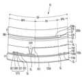
도 11은 제1 편광층(120b)이 표시 영역(DA)에 배치되는 복수의 금속선(121b)과 비표시 영역(PDA)에 배치되는 금속 피스(122b)를 포함하는 것을 예시한다. 복수의 금속선(121b)은 도 10의 제1 편광층(120a)을 구성하는 복수의 금속선과 동일하다. 금속 피스(122b)는 복수의 금속선(121b)의 형성시 함께 형성될 수 있으며, 복수의 금속선(121b)과 동일한 높이를 가질 수 있다. 이러한 제1 편광층(120b)은 비표시 영역(NDA)에서 표면적이 큰 금속 피스(122b)를 가지기 때문에, 표시 영역(DA)에 배치된 복수의 금속선(121b)으로부터 반사된 광과 비표시 영역(NDA)에 배치된 금속 피스(122b)으로부터 반사된 광이 제1 편광층(120b)으로 재입사될 수 있으므로 광 이용 효율이 크게 향상될 수 있다.11 illustrates that the first
도 12는 제1 편광층(120c)이 제1 전극(PE), 구체적으로 제1 서브 전극(PE1)과 제2 서브 전극(PE2) 상에 배치되는 복수의 금속선(121c)과, 표시 영역(DA)에서 제1 전극(PE)이 배치된 영역을 제외한 영역과 비표시 영역(NDA)에 배치되는 금속 피스(122c)를 포함하는 것을 예시한다. 금속 피스(122c)는 복수의 금속선(121c)의 형성시 함께 형성될 수 있으며, 복수의 금속선(121c)과 동일한 높이를 가질 수 있다. 이러한 제1 편광층(120c)은 표시 영역(DA)에서 제1 전극(PE)이 배치된 영역을 제외한 영역과 비표시 영역(NDA)에서 표면적이 큰 금속 피스(122c)를 가지기 때문에, 표시 영역(DA)에 배치된 복수의 금속선(121c)으로부터 반사된 광과 비표시 영역(NDA)에 배치된 금속 피스(122c)으로부터 반사된 광이 제1 편광층(120c)으로 재입사될 수 있으므로 광 이용 효율이 더욱 크게 향상될 수 있다.12 shows a state in which the first
표시 패널(11)의 제2 표시판(200)은 도 5에서 구체적으로 설명되었으므로, 중복된 설명은 생략하기로 한다.Since the
상기와 같이 본 발명의 다른 실시예에 따른 곡면 표시 장치는 제1 기판(110)과 액정층(LC) 사이에 복수의 금속선으로 구성되는 제1 편광층(120a)을 구비함으로써, 제1 기판(110) 상에 제1 편광층(120a)의 형성을 용이하게 하면서 광 이용 효율을 높일 수 있고, 제1 기판(110)에 광학적 이방성 현상이 발생하더라도 제1 편광층(120a)의 편광 특성이 유지된 광을 액정층(LC)에 제공하게 할 수 있다.As described above, the curved display device according to another embodiment of the present invention includes the first
따라서, 본 발명의 다른 실시예에 따른 곡면 표시 장치는 제1 편광층이 제1 기판의 외부에 배치되는 경우 제1 기판의 광학적 이방성 현상으로 인해 제1 편광층에 의해 편광된 광에 위상 지연이 발생된 광(제1 편광층의 편광 특성과 다른 편광 특성을 가지는 광)이 액정층을 통과함으로써 원하지 않는 영상이 표시되게 하는 것, 예를 들어 블랙 영상에 빛샘 현상이 발생되게 하는 것을 줄일 수 있다.Therefore, in the curved display device according to another embodiment of the present invention, when the first polarizing layer is disposed outside the first substrate, a phase retardation is caused in the light polarized by the first polarizing layer due to the optical anisotropy of the first substrate It is possible to reduce unwanted images to be displayed by passing the generated light (light having a polarizing characteristic different from that of the first polarizing layer) through the liquid crystal layer, for example, causing light leakage to occur in the black image .
다음은 본 발명의 또다른 실시예에 따른 곡면 표시 장치에 대해 설명하기로 한다.Next, a curved display device according to another embodiment of the present invention will be described.
도 13은 본 발명의 또다른 실시예에 따른 곡면 표시 장치 중 도 5의 표시 패널과 대응되는 표시 패널의 단면도이다.13 is a cross-sectional view of a display panel corresponding to the display panel of FIG. 5 of a curved surface display device according to another embodiment of the present invention.
도 13을 참조하면, 본 발명의 또다른 실시예에 따른 곡면 표시 장치는 도 2의 곡면 표시 장치(50)와 비교하여 표시 패널(12)만 다르며 동일한 구성을 가진다. 이에 따라, 본 발명의 또다른 실시예에 따른 곡면 표시 장치에서는 표시 패널(12)에 대해서만 설명하기로 한다.Referring to FIG. 13, the curved surface display device according to another embodiment of the present invention is different from the curved
표시 패널(12)의 제1 표시판(100)은 상호 대향하는 제1 표시판(100d) 및 제2 표시판(200a)을 포함할 수 있다. 제1 표시판(100d)과 제2 표시판(200a)은 실링재(미도시)에 의해 결합할 수 있다. 제1 표시판(100d)과 제2 표시판(200a) 사이에는 액정층(LC)이 개재될 수 있다.The
표시 패널(12)의 제1 표시판(100d)은 제1 기판(110), 제1 편광층(120d), 제1 절연층(130d), 게이트 라인(GL), 데이터 라인(DL), 스토리지 라인(SL), 기준 라인(RL), 게이트 절연층(140), 제1 박막트랜지스터(TFT1), 제2 박막트랜지스터(TFT2), 제3 박막트랜지스터(TFT3), 보호층(150) 및 제1 전극(PE)을 포함하며, 도 5의 제1 표시판(100)과 유사하다.The
다만, 제1 편광층(120d)은 제1 기판(110)의 외측에 배치된다. 이에 따라, 제1 편광층(120d)은 백라이트 유닛(20)으로부터 제공되는 내부광을 소정의 특정 방향으로 편광시켜, 편광된 광을 제1 기판(110)에 제공한다. 이에 따라, 제1 기판(110)에 광학적 이방성 현상이 발생되는 경우, 제1 편광층(120d)에 의해 편광된 광이 제1 기판(110)을 통과시 제1 편광층(120d)에 의해 편광된 광에 위상 지연이 발생될 수 있다. 이로 인해 위상 지연이 발생된 광이 액정층(LC)에 제공되어, 액정층(LC)에 제공되는 광의 편광 특성이 제1 편광층(120d)에 의해 편광된 광의 편광 특성과 달라질 수 있다. 이는, 제2 편광층(230a)의 의해 편광된 광에 원하지 않는 광이 미미하게 포함되게 할 수 있다. 예를 들어, 곡면 표시 장치가 블랙 영상을 표시하도록 액정층(LC)의 액정 분자들의 배열이 제어된 경우에서, 블랙 영상에 미미한 빛샘 현상이 발생될 수 있다. 상기 미미한 빛샘 현상은 크게 인식되지는 않는다.However, the first
제1 편광층(120d)은 제1 편광층(120)과 같이 흡수형 편광층이거나 반사형 편광층일 수 있다. 도 13에서는, 제1 편광층(120d)이 0°의 광축(도 6의 OA1)을 가지는 흡수형 편광층으로 형성된 경우가 예시되었다. 제1 편광층(120d)은 제1 기판(110) 상에 전면적으로 배치될 수 있으나, 이에 한정되는 것은 아니다. 몇몇 실시예에서, 제1 편광층(120d)은 표시 영역(DA)과 대응되도록 배치될 수 있다.The first
제1 절연층(130d)은 도 5의 제1 절연층(130)과 유사하다. 다만, 제1 절연층(130d)은 제1 기판(110) 상에 직접 형성된다. 몇몇 실시예에서, 제1 절연층(130a)은 생략될 수도 있다.The first insulating
표시 패널(12)의 제2 표시판(200a)은 제2 기판(210), 블랙 매트릭스(BM), 컬러 필터(CF), 오버 코팅층(220), 제2 전극(CE) 및 제2 편광층(230a)을 포함하며, 도 5의 제2 표시판(200)과 유사하다.The
다만, 제2 편광층(230a)은 제2 기판(210)과 액정층(LC) 사이에 배치된다. 예를 들어, 제2 편광층(230a)은 제2 기판(210)과 컬러필터(CF) 사이에 형성될 수 있다. 즉, 제2 편광층(230a)은 제2 기판(210) 상에 컬러필터(CF)를 포함하는 다른 구성들보다 먼저 형성되어, 제2 편광층(230a)의 형성시 다른 구성들을 형성하기 위해 가해지는 고온에 의한 영향을 받지 않을 수 있다. 또한, 제2 편광층(230a)은 제2 기판(210) 상에 직접 배치되어 제2 기판(210)의 평탄면에 용이하게 부착되거나, 제2 기판(210)의 평탄면에서 용이하게 제조될 수 있다However, the second
제2 편광층(230a)은 도 5의 편광층(230)과 유사한 역할을 한다. 다만, 제2 편광층(230a)은 제2 기판(210)과 액정층(LC) 사이에 배치되어 액정층(LC)을 통과한 광을 편광시켜 제2 기판(210)에 제공한다. 이에 따라, 제2 기판(210)에 광학적 이방성 현상이 발생되더라도, 제2 편광층(230a)은 제2 기판(210)의 광학적 이방성에 따른 광의 위상 지연에 상관 없이 액정층(LC)으로부터 제공되는 광을 편광시킬 수 있다. 이로 인해 제2 편광층이 제2 기판의 외부에 배치되어 위상 지연이 발생된 광을 편광시키는 경우에서 편광된 광에 원하지 않는 광이 포함되는 것이 줄어들 수 있다. 다만, 앞에서 설명한 바와 같이 제1 편광층(120d)에 의해 편광된 광의 편광 특성이 달라진 상태로 액정층(LC)에 제공되기 때문에, 제2 편광판(230a)에 의해 편광된 광에 원하지 않는 광이 미미하게 포함될 수 있지만, 이는 크게 인식되지 않는다.The second
제2 편광층(230a)은 흡수형 편광층이거나, 반사형 편광층일 수 있다. 도 13에서는, 제2 편광층(230a)이 90°의 광축(도 7의 OA2)을 가지는 흡수형 편광층으로 형성된 경우가 예시되었다. 제2 편광층(230a)은 제2 기판(230) 상에 전면적으로 배치될 수 있으나, 이에 한정되는 것은 아니다. 몇몇 실시예에서, 제2 편광층(230a)은 표시 영역(DA)과 대응되도록 배치될 수 있다.The second
상기와 같이 본 발명의 또다른 실시예에 따른 곡면 표시 장치는 제2 기판(210)과 액정층(LC) 사이에 형성되는 제2 편광층(230a)을 구비함으로써, 제2 기판(210)에 광학적 이방성 현상이 발생하더라도 제2 기판(210)의 광학적 이방성 현상에 따른 광의 위상 지연에 상관 없이 액정층(LC)으로부터 제공되는 광을 편광시킬 수 있다.As described above, the curved display device according to another embodiment of the present invention includes the second
따라서, 본 발명의 또다른 실시예에 따른 곡면 표시 장치는 제2 편광층이 제2 기판의 외부에 배치되는 경우 제2 기판의 광학적 이방성 현상으로 인해 위상 지연이 발생된 광이 제2 편광층에 제공되어 편광됨으로써 원하지 않는 영상이 표시되게 하는 것, 예를 들어 블랙 영상에 빛샘 현상이 발생되게 하는 것을 줄일 수 있다.Accordingly, in the curved display device according to another embodiment of the present invention, when the second polarizing layer is disposed outside the second substrate, light having a phase delay due to optical anisotropy of the second substrate is incident on the second polarizing layer It is possible to reduce the occurrence of a light leakage phenomenon in a black image, for example.
다음은 본 발명의 또다른 실시예에 따른 곡면 표시 장치에 대해 설명하기로 한다.Next, a curved display device according to another embodiment of the present invention will be described.
도 14는 본 발명의 또다른 실시예에 따른 곡면 표시 장치 중 도 5의 표시 패널과 대응되는 표시 패널의 단면도이고, 도 15는 도 14의 표시 패널을 설명하기 위한 한 화소의 평면도이다.FIG. 14 is a cross-sectional view of a display panel corresponding to the display panel of FIG. 5 and FIG. 15 is a plan view of one pixel for explaining the display panel of FIG. 14, according to another embodiment of the present invention.
도 14를 참조하면, 본 발명의 또다른 실시예에 따른 곡면 표시 장치는 도 2의 곡면 표시 장치(50)와 비교하여 표시 패널(13)만 다르며 동일한 구성을 가진다. 이에 따라, 본 발명의 또다른 실시예에 따른 곡면 표시 장치에서는 표시 패널(13)에 대해서만 설명하기로 한다.Referring to FIG. 14, the curved surface display device according to another embodiment of the present invention is different from the curved
표시 패널(13)의 상호 대향하는 제1 표시판(100d) 및 제2 표시판(200b)을 포함할 수 있다. 제1 표시판(100d)과 제2 표시판(200b)은 실링재(미도시)에 의해 결합할 수 있다. 제1 표시판(100d)과 제2 표시판(200b) 사이에는 액정층(LC)이 개재될 수 있다.And a
표시 패널(13)의 제1 표시판(100d)은 도 13에서 구체적으로 설명되었으므로, 중복된 설명은 생략하기로 한다.Since the
표시 패널(13)의 제2 표시판(200b)은 제2 기판(210), 블랙 매트릭스(BM), 컬러 필터(CF), 오버 코팅층(220), 제2 전극(CE) 및 제2 편광층(230b)을 포함하며, 도 5의 제2 표시판(200)과 유사하다.The
다만, 제2 편광층(230b)은 제2 기판(210)과 액정층(LC) 사이에 배치된다. 예를 들어, 제2 편광층(230b)은 제2 기판(210)과 컬러필터(CF) 사이에 형성될 수 있다. 즉, 제2 편광층(230b)은 제2 기판(210) 상에 컬러필터(CF)를 포함하는 다른 구성들보다 먼저 형성되어, 제2 편광층(230b)의 형성시 다른 구성들을 형성하기 위해 가해지는 고온에 의한 영향을 받지 않을 수 있다. 또한, 제2 편광층(230b)은 제2 기판(210) 상에 직접 배치되어 제2 기판(210)의 평탄면에 용이하게 부착되거나, 제2 기판(210)의 평탄면에서 용이하게 제조될 수 있다However, the second
제2 편광층(230b)은 도 5의 편광층(230)과 유사한 역할을 한다. 다만, 제2 편광층(230b)은 제2 기판(210)과 액정층(LC) 사이에 배치되어 액정층(LC)을 통과한 광을 편광시켜 제2 기판(210)에 제공한다. 이에 따라, 제2 기판(210)에 광학적 이방성 현상이 발생되더라도, 제2 편광층(230b)은 제2 기판(210)의 광학적 이방성에 따른 광의 위상 지연에 상관 없이 액정층(LC)으로부터 제공되는 광을 편광시킬 수 있다. 이로 인해 제2 편광층이 제2 기판의 외부에 배치되어 위상 지연이 발생된 광을 편광시키는 경우에서 편광된 광에 원하지 않는 광이 포함되는 것이 줄어들 수 있다. 다만, 앞에서 설명한 바와 같이 제1 편광층(120d)에 의해 편광된 광의 편광 특성이 달라진 상태로 액정층(LC)에 제공되기 때문에, 제2 편광판(230b)에 의해 편광된 광에 원하지 않는 광이 미미하게 포함될 수 있지만, 이는 크게 인식되지 않는다.The second
제2 편광층(230b)은 상기 특정 방향과 수직인 방향으로 편광시키는 광 이외의 광을 흡수시키는 흡수형 편광층이거나, 상기 특정 방향과 수직인 방향으로 편광시키는 광 이외의 광을 반사시키는 반사형 편광층일 수 있다. 도 14 및 도 15에서는, 제2 편광층(230b)이 90°의 광축(OA2)을 가지는 반사형 편광층으로 형성된 경우가 예시되었다. 이때, 제2 편광층(230b)은 제1 전극(PE), 구체적으로 제1 서브 전극(PE1)과 제2 서브 전극(PE2) 상에만 배치되되 도 9의 복수의 금속선과 수직인 복수의 금속선을 포함할 수 있다. 이에 따라, 제2 편광층(230b)이 반사형 편광층으로 형성된 경우에서, 제2 편광층(230b)으로 입사되는 외부광이 제2 편광층(230a)으로부터 반사됨으로 인해 눈부심 현상이 발생되는 것이 최소화될 수 있다. 한편, 제2 편광층(230b)를 구성하는 상기 복수의 금속선이 제1 전극(PE), 구체적으로 제1 서브 전극(PE1)과 제2 서브 전극(PE2) 상에만 배치 경우, 제2 편광층(230b)은 블랙 매트릭스(BM)와 동일 레벨에 있을 수 있다.The second
상기와 같이 본 발명의 또다른 실시예에 따른 곡면 표시 장치는 제2 기판(210)과 액정층(LC) 사이에 형성되는 제2 편광층(230b)을 구비함으로써, 눈부심 현상이 발생되는 것을 최소화하면서 제2 기판(210)에 광학적 이방성 현상이 발생하더라도 제2 기판(210)의 광학적 이방성 현상에 따른 광의 위상 지연에 상관 없이 액정층(LC)으로부터 제공되는 광을 편광시킬 수 있다.As described above, the curved display device according to another embodiment of the present invention includes the second
따라서, 본 발명의 또다른 실시예에 따른 곡면 표시 장치는 제2 편광층이 제2 기판의 외부에 배치되는 경우 제2 기판의 광학적 이방성 현상으로 인해 위상 지연이 발생된 광이 제2 편광층에 제공되어 편광됨으로써 원하지 않는 영상이 표시되게 하는 것, 예를 들어 블랙 영상에 빛샘 현상이 발생되게 하는 것을 줄일 수 있다.Accordingly, in the curved display device according to another embodiment of the present invention, when the second polarizing layer is disposed outside the second substrate, light having a phase delay due to optical anisotropy of the second substrate is incident on the second polarizing layer It is possible to reduce the occurrence of a light leakage phenomenon in a black image, for example.
다음은 본 발명의 또다른 실시예에 따른 곡면 표시 장치에 대해 설명하기로 한다.Next, a curved display device according to another embodiment of the present invention will be described.
도 16은 본 발명의 또다른 실시예에 따른 곡면 표시 장치 중 도 5의 표시 패널과 대응되는 표시 패널의 단면도이다.FIG. 16 is a sectional view of a display panel corresponding to the display panel of FIG. 5 of a curved surface display device according to another embodiment of the present invention.
도 16을 참조하면, 본 발명의 또다른 실시예에 따른 곡면 표시 장치는 도 2의 곡면 표시 장치(50)와 비교하여 표시 패널(14)만 다르며 동일한 구성을 가진다. 이에 따라, 본 발명의 다른 실시예에 따른 곡면 표시 장치에서는 표시 패널(14)에 대해서만 설명하기로 한다.Referring to FIG. 16, the curved surface display device according to another embodiment of the present invention is different from the curved
표시 패널(14)는 상호 대향하는 제1 표시판(100a) 및 제2 표시판(200b)을 포함할 수 있다. 제1 표시판(100a)과 제2 표시판(200b)은 실링재(미도시)에 의해 결합할 수 있다. 제1 표시판(100a)과 제2 표시판(200b) 사이에는 액정층(LC)이 개재될 수 있다.The
표시 패널(14)의 제1 표시판(100a)은 도 8에서 구체적으로 설명되었으므로, 중복된 설명은 생략하기로 한다.Since the
표시 패널(14)의 제2 표시판(200b)은 도 14에서 구체적으로 설명되었으므로, 중복된 설명은 생략하기로 한다.Since the
다만, 표시 패널(14)에서는 액정층(LC)에 제공되는 광의 편광 특성이 제1 편광층(120a)에 의해 편광된 광의 편광 특성을 가지며 액정층(LC)을 통과한 광이 제2 기판(210)에 제공되기 전에 제2 편광층(230b)에 제공되므로, 액정층(LC)을 통과한 광이 광학적 이방성 현상을 가지는 제2 기판(210)의 영향 없이 제2 편광층(230b)에 의해 편광될 수 있다.However, in the
이에 따라, 곡면 표시 장치에서 원하는 영상, 예를 들어 블랙 영상을 표시하도록 액정층(LC)의 액정 분자들의 배열이 제어된 경우에서 액정층(LC)을 통과한 광이 제2 편광층(230b)을 통과하지 않아 빛샘 없는 블랙 영상이 표시될 수 있다.Accordingly, when the arrangement of the liquid crystal molecules of the liquid crystal layer LC is controlled so as to display a desired image, for example, a black image, in the curved display device, light having passed through the liquid crystal layer LC is transmitted through the second
상기와 같이 본 발명의 또다른 실시예에 따른 곡면 표시 장치는 제1 기판(110)과 액정층(LCL) 사이에 형성되는 제1 편광층(120a)과 제2 기판(210)과 액정층(LC) 사이에 형성되는 제2 편광층(230b)을 구비함으로써, 제1 기판(110)에 광학적 이방성 현상이 발생하더라도 제1 편광층(120a)의 편광 특성이 유지된 광을 액정층(LC)에 제공하게 할 수 있으며, 또한 제2 기판(210)에 광학적 이방성 현상이 발생하더라도 제2 기판(210)의 광학적 이방성 현상에 따른 광의 위상 지연에 상관 없이 액정층(LC)으로부터 제공되는 광을 편광시킬 수 있다.As described above, the curved display device according to another embodiment of the present invention includes the first
따라서, 본 발명의 또다른 실시예에 따른 곡면 표시 장치는 제1 기판(110)의 광학적 이방성 현상과 제2 기판(230)의 광학적 이방성 현상에 의해 원하지 않는 영상이 표시되게 하는 것, 예를 들어 블랙 영상에 빛샘 현상이 발생되게 하는 것을 최소화시킬 수 있다.Accordingly, the curved display device according to another embodiment of the present invention may be configured to display an optical anisotropy of the
다음은 본 발명의 또다른 실시예에 따른 곡면 표시 장치에 대해 설명하기로 한다.Next, a curved display device according to another embodiment of the present invention will be described.
도 17은 본 발명의 또다른 실시예에 따른 곡면 표시 장치 중 도 5의 표시 패널과 대응되는 표시 패널의 단면도이다.17 is a sectional view of a display panel corresponding to the display panel of FIG. 5 of a curved surface display device according to another embodiment of the present invention.
도 17을 참조하면, 본 발명의 또다른 실시예에 따른 곡면 표시 장치는 도 2의 곡면 표시 장치(50)와 비교하여 표시 패널(15)만 다르며 동일한 구성을 가진다. 이에 따라, 본 발명의 다른 실시예에 따른 곡면 표시 장치에서는 표시 패널(15)에 대해서만 설명하기로 한다.Referring to FIG. 17, the curved surface display device according to another embodiment of the present invention is different from the curved
표시 패널(15)은 상호 대향하는 제1 표시판(100e) 및 제2 표시판(200b)을 포함할 수 있다. 제1 표시판(100e)과 제2 표시판(200b)은 실링재(미도시)에 의해 결합할 수 있다. 제1 표시판(100e)과 제2 표시판(200b) 사이에는 액정층(LC)이 개재될 수 있다.The
표시 패널(15)은 제1 기판(110e), 제1 편광층(120d), 제1 절연층(130d), 게이트 라인(GL), 데이터 라인(DL), 스토리지 라인(SL), 기준 라인(RL), 게이트 절연층(140), 제1 박막트랜지스터(TFT1), 제2 박막트랜지스터(TFT2), 제3 박막트랜지스터(TFT3), 보호층(150) 및 제1 전극(PE)을 포함하며, 도 14의 제1 표시판(100d)과 유사하다.The
다만, 제1 기판(110e)은 도 14의 제1 기판(110a)의 제1 두께(t1)보다 얇은 제1 두께(t11)를 가진다. 즉, 제1 기판(110e)의 제1 두께(t11)는 제2 기판(210)의 제2 두께(t2)보다 얇을 수 있다. 이 경우, 곡률을 가지는 백라이트 유닛(20)에 평평한 표시 패널(13)을 체결하여 곡면 표시 장치를 제조하는 과정에서 제1 기판(110e)에 발생되는 제1 스트레스는 제2 기판(210)에 발생되는 제2 스트레스보다 작을 수 있다.However, the
이로 인해, 제1 기판(110e)에 광학적 이방성 현상이 형성되는 것이 줄어들 수 있다. 이에 따라, 제1 편광층(120d)이 제1 기판(110e)의 외부에 배치되더라도, 제1 편광판(120d)에 의해 편광된 내부광이 광학적 이방성을 가지는 제1 기판(110e)을 통과시 제1 편광판(120d)에 의해 편광된 내부광에 위상 지연이 크게 발생되지 않을 수 있다.Thus, the formation of the optical anisotropy phenomenon on the
표시 패널(15)의 제2 표시판(200b)은 도 14에서 구체적으로 설명되었으므로, 중복된 설명은 생략하기로 한다.Since the
상기와 같이 본 발명의 또다른 실시예에 따른 곡면 표시 장치는 제1 기판(110e)의 제1 두께(t11)를 제2 기판(210)의 제2 두께(t2)보다 얇게 하여 제1 기판(110e)에 발생되는 제1 스트레스를 제2 기판(210)의 제2 스트레스보다 작게 할 수 있다As described above, the curved surface display device according to another embodiment of the present invention is configured such that the first thickness t11 of the
따라서, 본 발명의 또다른 실시예에 따른 곡면 표시 장치는 제1 기판(110e)의 광학적 이방성 현상으로 인해 제1 편광층(120d)에 의해 편광된 광의 위상 지연이 발생하는 것을 줄여 위상 지연이 줄어든 광이 액정층에 제공되게 할 수 있으며, 또한 슬림한 곡면 표시 장치를 구현하게 할 수 있다.Therefore, the curved display device according to another embodiment of the present invention reduces the phase delay of light polarized by the first
다음은 본 발명의 또다른 실시예에 따른 곡면 표시 장치에 대해 설명하기로 한다.Next, a curved display device according to another embodiment of the present invention will be described.
도 18은 본 발명의 또다른 실시예에 따른 곡면 표시 장치 중 도 5의 표시 패널과 대응되는 표시 패널의 단면도이다.FIG. 18 is a sectional view of a display panel corresponding to the display panel of FIG. 5 among the curved surface display devices according to another embodiment of the present invention.
도 18을 참조하면, 본 발명의 또다른 실시예에 따른 곡면 표시 장치는 도 2의 곡면 표시 장치(50)와 비교하여 표시 패널(16)만 다르며 동일한 구성을 가진다. 이에 따라, 본 발명의 다른 실시예에 따른 곡면 표시 장치에서는 표시 패널(15)에 대해서만 설명하기로 한다.Referring to FIG. 18, the curved surface display device according to another embodiment of the present invention is different from the curved
표시 패널(16)은 상호 대향하는 제1 표시판(100f) 및 제2 표시판(200c)을 포함할 수 있다. 제1 표시판(100f)과 제2 표시판(200c)은 실링재(미도시)에 의해 결합할 수 있다. 제1 표시판(100f)과 제2 표시판(200c) 사이에는 액정층(LC)이 개재될 수 있다.The
표시 패널(16)은 제1 기판(110), 제1 편광층(120a), 제1 절연층(130a), 게이트 라인(GL), 데이터 라인(DL), 스토리지 라인(SL), 기준 라인(RL), 게이트 절연층(140), 제1 박막트랜지스터(TFT1), 제2 박막트랜지스터(TFT2), 제3 박막트랜지스터(TFT3), 제2 절연층(160f), 블랙 매트릭스(BM), 컬러 필터(CF), 평탄화층(170f) 및 제1 전극(PE)을 포함하며, 도 8의 제1 표시판(100a)과 유사하다.The
다만, 제2 절연층(160f)은 제1 박막트랜지스터(TFT1), 제2 박막트랜지스터(TFT2) 및 제3 박막트랜지스터(TFT3) 상에 형성되고, 도 8의 제2 표시판(200)에 포함된 블랙 매트릭스(BM)와 컬러 필터(CF)가 제1 표시판(100f)의 제2 절연층(160f) 상에 형성되며, 블랙 매트릭스(BM)와 컬러 필터(CF)를 평탄화시키는 평탄화층(170f)이 형성된다. 이 때, 블랙 매트릭스(BM)는 게이트 라인(GL), 데이터 라인(DL) 및 박막 트랜지스터들(TFT1, TFT2, TFT3)과 중첩할 수 있다.The second
표시 패널(16)의 제2 표시판(200c)은 제2 기판(210c), 제2 편광층(230) 및 제2 전극(CE)을 포함하며, 도 8의 제2 표시판(200)과 유사하다.The
다만, 제2 표시판(200c)의 구성이 도 8의 제2 표시판(200)의 구성보다 줄어들어, 제2 기판(210c)은 제1 기판(110)의 제1 두께(t)보다 얇은 제2 두께(t12)로 형성될 수 있다. 이 경우, 곡률을 가지는 백라이트 유닛(20)에 평평한 표시 패널(16)을 체결하여 곡면 표시 장치를 제조하는 과정에서 제2 기판(210c)에 발생되는 제2 스트레스는 제1 기판(110)에 발생되는 제1 스트레스보다 작을 수 있다.8, the
이로 인해, 제2 기판(210c)에 광학적 이방성 현상이 형성되는 것이 줄어들 수 있다. 이에 따라, 제2 편광층(230)이 제2 기판(210c)의 외부에 배치되더라도, 액정층(LC)으로부터 제공된 광이 광학적 이방성을 가지는 제2 기판(210c)을 통과시 제2 기판(210c)를 통과한 광에 위상 지연이 크게 발생되지 않을 수 있다.Thus, the formation of an optical anisotropy phenomenon on the
상기와 같이 본 발명의 또다른 실시예에 따른 곡면 표시 장치는 제2 기판(210c)의 제2 두께(t12)를 제1 기판(110)의 제1 두께(t1)보다 얇게 하여 제2 기판(210c)에 발생되는 제2 스트레스를 제1 기판(110)의 제1 스트레스보다 작게 할 수 있다As described above, the curved surface display device according to another embodiment of the present invention is configured such that the second thickness t12 of the
따라서, 본 발명의 또다른 실시예에 따른 곡면 표시 장치는 제2 기판(210c)의 광학적 이방성 현상으로 인해 액정층(LC)으로부터 제공되어 제2 기판(210c)을 통과하는 광의 위상 지연이 발생하는 것을 줄여 제2 편광층(230)에 제공되게 할 수 있으며, 또한 슬림한 곡면 표시 장치를 구현하게 할 수 있다.Therefore, the curved display device according to another embodiment of the present invention is provided from the liquid crystal layer LC due to the optical anisotropy of the
이상 첨부된 도면을 참조하여 본 발명의 실시예들을 설명하였지만, 본 발명이 속하는 기술분야에서 통상의 지식을 가진 자는 본 발명의 그 기술적 사상이나 필수적인 특징을 변경하지 않고서 다른 구체적인 형태로 실시될 수 있다는 것을 이해할 수 있을 것이다. 그러므로 이상에서 기술한 실시예들은 모든 면에서 예시적인 것이며 한정적이 아닌 것으로 이해해야만 한다.While the present invention has been described in connection with what is presently considered to be practical exemplary embodiments, it is to be understood that the invention is not limited to the disclosed embodiments, but, on the contrary, You will understand. It is therefore to be understood that the above-described embodiments are illustrative in all aspects and not restrictive.
10, 11 12, 13, 14, 15, 16: 표시 패널
20: 백라이트 유닛
30: 중간 수납 용기
40: 상부 수납 용기
50: 곡면 표시 장치
100, 100a, 100d, 100e, 100f: 제1 표시판
110, 110e: 제1 기판
120, 120a, 120b, 120c, 120d: 제1 편광층
130, 130a, 130d: 제1 절연층
140: 게이트 절연층
150: 보호층 160f: 제2 절연층
170f: 평탄화층
200, 200a, 200b, 200c: 제2 표시판
210, 210c: 제2 기판 220: 오버 코팅층
230, 230a, 230b: 제2 편광층10, 11 12, 13, 14, 15, 16: display panel
20: Backlight unit
30: Middle storage container
40: upper storage container
50: Surface display device
100, 100a, 100d, 100e, 100f: first display panel
110, 110e: a first substrate
120, 120a, 120b, 120c and 120d: a first polarizing layer
130, 130a, 130d: a first insulating layer
140: gate insulating layer
150:
170f: planarization layer
200, 200a, 200b, 200c: second display panel
210, 210c: second substrate 220: overcoat layer
230, 230a, and 230b: a second polarizing layer
Claims (20)
Translated fromKorean상기 제1 기판과 상기 제2 기판 사이에 배치되는 액정층;
상기 제1 기판과 상기 액정층 사이 또는 상기 제1 기판의 외측에 배치되는 제1 편광층; 및
상기 제2 기판과 상기 액정층 사이 또는 상기 제2 기판의 외측에 배치되는 제2 편광층을 포함하되,
상기 제1 편광층과 상기 제2 편광층 중 적어도 어느 하나가 상기 제1 기판과 액정층 사이 또는 상기 제2 기판과 상기 액정층 사이에 배치되는 곡면 표시 장치.A first substrate and a second substrate facing each other and having a curvature at least in part;
A liquid crystal layer disposed between the first substrate and the second substrate;
A first polarizing layer disposed between the first substrate and the liquid crystal layer or outside the first substrate; And
And a second polarizing layer disposed between the second substrate and the liquid crystal layer or outside the second substrate,
Wherein at least one of the first polarizing layer and the second polarizing layer is disposed between the first substrate and the liquid crystal layer or between the second substrate and the liquid crystal layer.
상기 제1 기판의 두께와 상기 제2 기판의 두께가 같은 곡면 표시 장치.The method according to claim 1,
Wherein the thickness of the first substrate is equal to the thickness of the second substrate.
상기 제1 편광층은 상기 제1 기판과 상기 액정층 사이에 배치되고,
상기 제2 편광층은 상기 제2 기판의 외측에 배치되는 곡면 표시 장치.3. The method of claim 2,
Wherein the first polarizing layer is disposed between the first substrate and the liquid crystal layer,
And the second polarizing layer is disposed outside the second substrate.
상기 제1 편광층은 상기 제1 기판의 외측에 배치되고,
상기 제2 편광층은 상기 제2 기판과 상기 액정층 사이에 배치되는 곡면 표시 장치.3. The method of claim 2,
Wherein the first polarizing layer is disposed outside the first substrate,
And the second polarizing layer is disposed between the second substrate and the liquid crystal layer.
상기 제1 편광층은 상기 제1 기판과 상기 액정층 사이에 배치되고,
상기 제2 편광층은 상기 제2 기판과 상기 액정층 사이에 배치되는 곡면 표시 장치.3. The method of claim 2,
Wherein the first polarizing layer is disposed between the first substrate and the liquid crystal layer,
And the second polarizing layer is disposed between the second substrate and the liquid crystal layer.
상기 제1 기판의 두께가 상기 제2 기판의 두께보다 작은 곡면 표시 장치.The method according to claim 1,
Wherein the thickness of the first substrate is smaller than the thickness of the second substrate.
상기 제1 편광층은 상기 제1 기판의 외측에 배치되고,
상기 제2 편광층은 상기 제2 기판과 상기 액정층 사이에 배치되는 곡면 표시 장치.The method according to claim 6,
Wherein the first polarizing layer is disposed outside the first substrate,
And the second polarizing layer is disposed between the second substrate and the liquid crystal layer.
상기 제2 기판의 두께가 상기 제1 기판의 두께보다 작은 곡면 표시 장치.The method according to claim 1,
Wherein the thickness of the second substrate is smaller than the thickness of the first substrate.
상기 제1 편광층은 상기 제1 기판과 상기 액정층 사이에 배치되고,
상기 제2 편광층은 상기 제2 기판의 외측에 배치되는 곡면 표시 장치.9. The method of claim 8,
Wherein the first polarizing layer is disposed between the first substrate and the liquid crystal layer,
And the second polarizing layer is disposed outside the second substrate.
상기 제1 편광층은 상기 제1 기판과 상기 액정층 사이에 배치되며, 상기 제1 기판에 직접 접촉하는 곡면 표시 장치.The method according to claim 1,
Wherein the first polarizing layer is disposed between the first substrate and the liquid crystal layer, and is in direct contact with the first substrate.
상기 제1 편광층과 상기 액정층 사이에 배치되는 박막트랜지스터들을 더 포함하며,
상기 제1 편광층은 상기 제1 기판과 상기 박막트랜지스터들 사이에 배치되는 곡면 표시 장치.The method according to claim 1,
Further comprising thin film transistors disposed between the first polarizing layer and the liquid crystal layer,
Wherein the first polarizing layer is disposed between the first substrate and the thin film transistors.
상기 제2 편광층은 상기 제2 기판과 상기 액정층 사이에 배치되며, 상기 제2 기판에 직접 접촉하는 곡면 표시 장치.The method according to claim 1,
Wherein the second polarizing layer is disposed between the second substrate and the liquid crystal layer, and is in direct contact with the second substrate.
상기 제1 편광층은 제1 광축을 가지도록 형성되며, 상기 제2 편광층은 상기 제1 광축과 수직인 제2 광축을 가지도록 형성되는 곡면 표시 장치.The method according to claim 1,
Wherein the first polarizing layer is formed to have a first optical axis and the second polarizing layer is formed to have a second optical axis perpendicular to the first optical axis.
상기 제1 기판의 하부에 배치되며 광을 공급하는 백라이트 유닛을 더 포함하는 곡면 표시 장치.17. The method of claim 16,
And a backlight unit disposed below the first substrate and supplying light.
상기 제1 기판은 영상을 표시하며 복수의 화소가 정의된 표시 영역과, 상기 표시 영역의 적어도 일측에 위치하는 비표시 영역을 포함하는 곡면 표시 장치.The method according to claim 1,
Wherein the first substrate includes a display region displaying an image and defining a plurality of pixels, and a non-display region located at least one side of the display region.
상기 제1 편광층은 흡수형 편광층이며, 상기 제2 편광층은 흡수형 편광층이고,
상기 제1 편광층과 상기 제2 편광층은 상기 제1 기판 상에 전면적으로 배치되거나 상기 제1 기판 상에 표시 영역과 중첩되게 배치되는 곡면 표시 장치.16. The method of claim 15,
Wherein the first polarizing layer is an absorption type polarizing layer, the second polarizing layer is an absorption type polarizing layer,
Wherein the first polarizing layer and the second polarizing layer are disposed on the first substrate over the entire surface or over the display region on the first substrate.
상기 제1 기판의 화소 단위로 배치되며, 상기 제1 편광층과 상기 액정층 사이에 배치되는 제1 전극을 더 포함하며,
상기 제1 편광층은 반사형 편광층이며, 상기 제2 편광층은 흡수형 편광층이고,
상기 제1 편광층은 상기 제1 기판 상에 전면적으로 배치되는 복수의 금속선으로 구성되거나, 상기 제1 기판 상에 상기 표시 영역과 중첩되게 배치되는 복수의 금속선을 포함하도록 구성되거나, 상기 제1 기판 상에 상기 제1 전극과 오버랩되게 배치되는 복수의 금속선을 포함하도록 구성되는 곡면 표시 장치.16. The method of claim 15,
And a first electrode disposed between the first polarizing layer and the liquid crystal layer, the first electrode being disposed on a pixel unit of the first substrate,
Wherein the first polarizing layer is a reflection type polarizing layer, the second polarizing layer is an absorption type polarizing layer,
The first polarizing layer may be composed of a plurality of metal lines disposed on the first substrate over the entire surface or may include a plurality of metal lines disposed on the first substrate so as to overlap with the display area, And a plurality of metal lines disposed on the first electrode so as to overlap with the first electrode.
상기 제1 기판의 화소 단위로 배치되며, 상기 제1 편광층과 상기 액정층 사이에 배치되는 제1 전극을 더 포함하며,
상기 제1 편광층은 흡수형 편광층이며, 상기 제2 편광층은 반사형 편광층이고,
상기 제2 편광층은 상기 제2 기판 상에 상기 제1 전극과 중첩되게 배치되는 복수의 금속선으로 구성되는 곡면 표시 장치.16. The method of claim 15,
And a first electrode disposed between the first polarizing layer and the liquid crystal layer, the first electrode being disposed on a pixel unit of the first substrate,
Wherein the first polarizing layer is an absorption type polarizing layer, the second polarizing layer is a reflection type polarizing layer,
And the second polarizing layer is composed of a plurality of metal wires arranged on the second substrate so as to overlap with the first electrode.
상기 제1 편광층과 상기 제1 전극 사이에 배치되는 박막트랜지스터들; 및
상기 제2 기판 상에서 상기 박막트랜지스터들과 중첩하게 배치되는 블랙 매트릭스를 더 포함하며,
상기 제1 전극은 평면상으로 상기 박막트랜지스터를 사이에 두고 배치되는 제1 서브 전극과 제2 서브 전극을 포함하고,
상기 제2 편광층은 상기 블랙 매트릭스와 동일 레벨에 있는 곡면 표시 장치.19. The method of claim 18,
Thin film transistors disposed between the first polarizing layer and the first electrode; And
Further comprising a black matrix disposed over the second substrate in superposition with the thin film transistors,
Wherein the first electrode includes a first sub-electrode and a second sub-electrode which are arranged in a plane on the substrate with the thin film transistor interposed therebetween,
And the second polarizing layer is at the same level as the black matrix.
상기 제1 기판의 화소 단위로 배치되며, 상기 제1 편광층과 상기 액정층 사이에 배치되는 제1 전극을 더 포함하며,
상기 제1 편광층은 반사형 편광층이며, 상기 제2 편광층은 반사형 편광층이고,
상기 제1 편광층은 상기 제1 기판 상에 전면적으로 배치되는 복수의 금속선으로 구성되거나 상기 제1 기판 상에 상기 표시 영역과 오버랩되게 배치되는 복수의 금속선을 포함하도록 구성되거나 상기 제1 기판 상에 상기 제1 전극과 오버랩되게 배치되는 복수의 금속선을 포함하도록 구성되며,
상기 제2 편광층은 상기 제2 기판 상에 상기 제1 전극과 오버랩되게 배치되는 복수의 금속선으로 구성되는 곡면 표시 장치.16. The method of claim 15,
And a first electrode disposed between the first polarizing layer and the liquid crystal layer, the first electrode being disposed on a pixel unit of the first substrate,
Wherein the first polarizing layer is a reflection type polarizing layer, the second polarizing layer is a reflection type polarizing layer,
The first polarizing layer may be configured to include a plurality of metal lines disposed on the first substrate over the entire surface or a plurality of metal lines disposed on the first substrate so as to overlap with the display area, And a plurality of metal lines arranged to overlap with the first electrode,
And the second polarizing layer is composed of a plurality of metal wires arranged on the second substrate so as to overlap with the first electrode.
Priority Applications (6)
| Application Number | Priority Date | Filing Date | Title |
|---|---|---|---|
| KR1020140156212AKR20160056460A (en) | 2014-11-11 | 2014-11-11 | Curved display device |
| US14/802,514US10254583B2 (en) | 2014-11-11 | 2015-07-17 | Curved display device |
| EP15179760.2AEP3021161B1 (en) | 2014-11-11 | 2015-08-05 | Curved liquid crystal display device with internal polarisers |
| JP2015173739AJP2016095492A (en) | 2014-11-11 | 2015-09-03 | Curved surface display device |
| CN201510651168.3ACN105589246A (en) | 2014-11-11 | 2015-10-09 | Curved display device |
| US16/287,789US10670913B2 (en) | 2014-11-11 | 2019-02-27 | Curved display device |
Applications Claiming Priority (1)
| Application Number | Priority Date | Filing Date | Title |
|---|---|---|---|
| KR1020140156212AKR20160056460A (en) | 2014-11-11 | 2014-11-11 | Curved display device |
Publications (1)
| Publication Number | Publication Date |
|---|---|
| KR20160056460Atrue KR20160056460A (en) | 2016-05-20 |
Family
ID=53776478
Family Applications (1)
| Application Number | Title | Priority Date | Filing Date |
|---|---|---|---|
| KR1020140156212ACeasedKR20160056460A (en) | 2014-11-11 | 2014-11-11 | Curved display device |
Country Status (5)
| Country | Link |
|---|---|
| US (2) | US10254583B2 (en) |
| EP (1) | EP3021161B1 (en) |
| JP (1) | JP2016095492A (en) |
| KR (1) | KR20160056460A (en) |
| CN (1) | CN105589246A (en) |
Cited By (1)
| Publication number | Priority date | Publication date | Assignee | Title |
|---|---|---|---|---|
| KR20200043582A (en)* | 2018-10-17 | 2020-04-28 | 삼성디스플레이 주식회사 | Liquid crystal display |
Families Citing this family (7)
| Publication number | Priority date | Publication date | Assignee | Title |
|---|---|---|---|---|
| CN105182594B (en)* | 2015-08-25 | 2018-07-31 | 京东方科技集团股份有限公司 | Display base plate |
| JP7097812B2 (en)* | 2016-07-15 | 2022-07-08 | ソニーグループ株式会社 | Display device |
| KR102744865B1 (en)* | 2016-12-01 | 2024-12-23 | 삼성디스플레이 주식회사 | Display device and method of manufacturing the same |
| DE102017207042B4 (en) | 2017-04-26 | 2024-05-16 | Audi Ag | Display device for a motor vehicle and motor vehicle |
| CN110573942B (en) | 2017-04-28 | 2022-05-13 | 株式会社Lg化学 | light modulation device |
| DE102018212445A1 (en)* | 2018-07-25 | 2020-03-05 | Volkswagen Aktiengesellschaft | Display and control device for a motor vehicle |
| JP2021182109A (en) | 2020-05-20 | 2021-11-25 | シャープ株式会社 | Curved surface display device |
Family Cites Families (52)
| Publication number | Priority date | Publication date | Assignee | Title |
|---|---|---|---|---|
| US4526818A (en)* | 1982-12-23 | 1985-07-02 | Epson Corporation | Liquid crystal display panel and process for the production thereof |
| US4674840A (en) | 1983-12-22 | 1987-06-23 | Polaroid Corporation, Patent Dept. | Liquid crystal display with polarizer and biaxial birefringent support |
| JP2808962B2 (en)* | 1991-08-19 | 1998-10-08 | 松下電器産業株式会社 | Liquid crystal panel alignment defect suppression method and display device |
| KR940011991A (en) | 1992-11-11 | 1994-06-22 | 이헌조 | Liquid crystal display device manufacturing method |
| KR950033669U (en) | 1994-05-27 | 1995-12-16 | 박향영 | Piping pipe noise prevention and expansion insulation clamp |
| JP3015792B1 (en)* | 1998-12-24 | 2000-03-06 | 株式会社東芝 | Display element |
| US6504592B1 (en)* | 1999-06-16 | 2003-01-07 | Nec Corporation | Liquid crystal display and method of manufacturing the same and method of driving the same |
| JP2001305526A (en)* | 2000-04-25 | 2001-10-31 | Seiko Epson Corp | Liquid crystal devices and electronic equipment |
| KR20030029251A (en)* | 2001-10-05 | 2003-04-14 | 삼성전자주식회사 | Liquid crystal display device |
| KR100944886B1 (en)* | 2001-10-30 | 2010-03-03 | 가부시키가이샤 한도오따이 에네루기 켄큐쇼 | Method for manufacturing semiconductor device |
| TW583466B (en)* | 2002-12-09 | 2004-04-11 | Hannstar Display Corp | Structure of liquid crystal display |
| TWI277042B (en) | 2003-10-28 | 2007-03-21 | Seiko Epson Corp | Electro-optical device, electronic equipment, and method of manufacturing electro-optical device |
| TWI377401B (en)* | 2005-01-25 | 2012-11-21 | Sumitomo Chemical Co | Liquid crystal display device and polarizing plate set useful for the same |
| JP5301080B2 (en)* | 2005-12-26 | 2013-09-25 | 株式会社ジャパンディスプレイ | Liquid crystal display |
| US8189141B2 (en)* | 2006-06-02 | 2012-05-29 | Semiconductor Energy Laboratory Co., Ltd. | Semiconductor device |
| JP5094250B2 (en)* | 2007-07-10 | 2012-12-12 | 株式会社ジャパンディスプレイイースト | Display device |
| JP5213407B2 (en) | 2007-10-10 | 2013-06-19 | 株式会社ジャパンディスプレイイースト | Liquid crystal display device and organic EL display device |
| JP5322427B2 (en) | 2007-12-19 | 2013-10-23 | 三菱電機株式会社 | Liquid crystal display |
| JP4950019B2 (en)* | 2007-12-27 | 2012-06-13 | 株式会社 日立ディスプレイズ | Liquid crystal display |
| JP4640446B2 (en)* | 2008-05-26 | 2011-03-02 | ソニー株式会社 | Liquid crystal device, color filter substrate and array substrate |
| JP2010032768A (en)* | 2008-07-29 | 2010-02-12 | Hitachi Displays Ltd | Image display and manufacturing method thereof |
| JP2010097028A (en) | 2008-10-17 | 2010-04-30 | Hitachi Displays Ltd | Liquid crystal display panel |
| KR20100054344A (en)* | 2008-11-14 | 2010-05-25 | 삼성전자주식회사 | Liquid crystal device and method for manufacturing the same |
| AU2010216235B2 (en) | 2009-02-17 | 2012-08-23 | 3M Innovative Properties Company | Optical control devices and methods of making |
| JP5591479B2 (en)* | 2009-03-13 | 2014-09-17 | 株式会社ジャパンディスプレイ | Liquid crystal display |
| KR101179436B1 (en)* | 2009-09-18 | 2012-09-04 | 주식회사 토비스 | Method for manufacturing display panel with curved shape |
| KR20110046130A (en)* | 2009-10-28 | 2011-05-04 | 삼성전자주식회사 | Liquid crystal display panel |
| KR101902984B1 (en)* | 2010-04-02 | 2018-11-14 | 삼성디스플레이 주식회사 | Pixel electrode panel, liquid crystal display panel assembly and methods for manufacturing the same |
| US20120050075A1 (en)* | 2010-08-24 | 2012-03-01 | Salmon Peter C | Retractable device |
| JP2012063670A (en)* | 2010-09-17 | 2012-03-29 | Hitachi Displays Ltd | Liquid crystal display device |
| US8827446B2 (en)* | 2011-03-10 | 2014-09-09 | Hpo Assets Llc | Electronic lens comprised of hybrid materials |
| CN102650823A (en)* | 2011-05-13 | 2012-08-29 | 京东方科技集团股份有限公司 | Color filter with polarization ability and manufacturing method thereof |
| KR101828066B1 (en) | 2011-05-19 | 2018-02-12 | 삼성디스플레이 주식회사 | Display apparatus |
| KR20130039066A (en)* | 2011-10-11 | 2013-04-19 | 삼성디스플레이 주식회사 | Display apparatus, display system having the same and method of manufacturing the display apparatus |
| US9194566B2 (en)* | 2012-06-08 | 2015-11-24 | Lg Innotek Co., Ltd. | Lamp unit and vehicle lamp apparatus using the same |
| KR102041883B1 (en) | 2012-07-09 | 2019-11-08 | 삼성디스플레이 주식회사 | Curved frame and curved display device having the same |
| KR101381610B1 (en)* | 2012-09-04 | 2014-04-04 | (주)코텍 | Bending method of liquid crystal display device |
| US9128327B2 (en)* | 2012-09-19 | 2015-09-08 | Apple Inc. | Stress insensitive liquid crystal display |
| KR20140043198A (en)* | 2012-09-28 | 2014-04-08 | 삼성디스플레이 주식회사 | Curved display apparatus |
| KR101961427B1 (en)* | 2012-10-29 | 2019-03-25 | 삼성디스플레이 주식회사 | Liquid crystal display and manufacturing method thereof |
| KR20140091100A (en)* | 2012-12-26 | 2014-07-21 | 삼성디스플레이 주식회사 | Curved liquid crystal display device |
| US20140254011A1 (en) | 2013-03-08 | 2014-09-11 | Ravenbrick, Llc | Fabrication of coatable wire grid polarizers |
| KR102082783B1 (en)* | 2013-07-23 | 2020-03-02 | 삼성디스플레이 주식회사 | Wire grid polarizer and organic light emitting display apparatus comprising the same |
| KR102235720B1 (en)* | 2013-12-17 | 2021-04-05 | 삼성디스플레이 주식회사 | Curved display apparatus |
| KR102134857B1 (en)* | 2013-12-17 | 2020-07-17 | 삼성디스플레이 주식회사 | Curved display apparatus |
| KR102256566B1 (en)* | 2013-12-18 | 2021-05-27 | 삼성디스플레이 주식회사 | Curved display device and method of manufacturing the same |
| KR102148417B1 (en)* | 2014-01-13 | 2020-08-27 | 삼성전자주식회사 | In-cell polarizer, liquid crystal display having the same and method of manufacturing liquid crystal display |
| KR102162367B1 (en)* | 2014-02-14 | 2020-10-07 | 삼성디스플레이 주식회사 | Curved Display Apparatus |
| US9634040B2 (en)* | 2014-06-09 | 2017-04-25 | Shenzhen China Star Optoelectronics Technology Co., Ltd. | Array substrate and curved display device |
| KR102197826B1 (en)* | 2014-09-03 | 2021-01-05 | 삼성디스플레이 주식회사 | Display device |
| KR20160072379A (en)* | 2014-12-12 | 2016-06-23 | 삼성디스플레이 주식회사 | Display substrate, display panel and method of manufacturing a polarizer |
| CN104516611A (en)* | 2014-12-23 | 2015-04-15 | 深圳市华星光电技术有限公司 | Capacitive embedded touch screen and display device |
- 2014
- 2014-11-11KRKR1020140156212Apatent/KR20160056460A/ennot_activeCeased
- 2015
- 2015-07-17USUS14/802,514patent/US10254583B2/enactiveActive
- 2015-08-05EPEP15179760.2Apatent/EP3021161B1/enactiveActive
- 2015-09-03JPJP2015173739Apatent/JP2016095492A/ennot_activeCeased
- 2015-10-09CNCN201510651168.3Apatent/CN105589246A/enactivePending
- 2019
- 2019-02-27USUS16/287,789patent/US10670913B2/ennot_activeExpired - Fee Related
Cited By (1)
| Publication number | Priority date | Publication date | Assignee | Title |
|---|---|---|---|---|
| KR20200043582A (en)* | 2018-10-17 | 2020-04-28 | 삼성디스플레이 주식회사 | Liquid crystal display |
Also Published As
| Publication number | Publication date |
|---|---|
| JP2016095492A (en) | 2016-05-26 |
| EP3021161B1 (en) | 2020-07-08 |
| EP3021161A1 (en) | 2016-05-18 |
| US10670913B2 (en) | 2020-06-02 |
| US10254583B2 (en) | 2019-04-09 |
| CN105589246A (en) | 2016-05-18 |
| US20190196266A1 (en) | 2019-06-27 |
| US20160131945A1 (en) | 2016-05-12 |
Similar Documents
| Publication | Publication Date | Title |
|---|---|---|
| TWI646520B (en) | Transparent display device | |
| KR20160056460A (en) | Curved display device | |
| US9559124B2 (en) | Display panel | |
| US8330898B2 (en) | Flexible liquid crystal display device | |
| US9519186B2 (en) | Display device including a color conversion layer | |
| US10336189B2 (en) | Polarizer plate and display device including the same | |
| CN104749839B (en) | It is bent liquid crystal display | |
| US9583738B2 (en) | Display device including reflecting layer | |
| US9625761B2 (en) | Polarizer and liquid crystal display including the same | |
| US20160124254A1 (en) | Display panel and thin film transistor array substrate included in the same | |
| US10634945B2 (en) | Reflective liquid crystal display | |
| US10241370B2 (en) | Semiconductor device and projection-type display unit | |
| US9104081B2 (en) | Liquid crystal display device and method of manufacturing the same | |
| US8570463B2 (en) | Liquid crystal display device | |
| US10747049B2 (en) | Display device | |
| KR102167689B1 (en) | Display panel and display device having the same | |
| US20140253854A1 (en) | Liquid crystal display | |
| JP2018194717A (en) | Electro-optic device and electronic apparatus | |
| US11703729B2 (en) | Display device | |
| KR102522531B1 (en) | Mirror display panel | |
| KR102485632B1 (en) | Display Device | |
| KR20120067754A (en) | Liquid crystal display device | |
| KR20110093056A (en) | Backlight unit and liquid crystal display device using the same |
Legal Events
| Date | Code | Title | Description |
|---|---|---|---|
| PA0109 | Patent application | Patent event code:PA01091R01D Comment text:Patent Application Patent event date:20141111 | |
| PG1501 | Laying open of application | ||
| PA0201 | Request for examination | Patent event code:PA02012R01D Patent event date:20191018 Comment text:Request for Examination of Application Patent event code:PA02011R01I Patent event date:20141111 Comment text:Patent Application | |
| E902 | Notification of reason for refusal | ||
| PE0902 | Notice of grounds for rejection | Comment text:Notification of reason for refusal Patent event date:20200911 Patent event code:PE09021S01D | |
| E601 | Decision to refuse application | ||
| PE0601 | Decision on rejection of patent | Patent event date:20210225 Comment text:Decision to Refuse Application Patent event code:PE06012S01D Patent event date:20200911 Comment text:Notification of reason for refusal Patent event code:PE06011S01I |