KR20160042570A - Physical vapor deposition apparatus and method of depositing phase-change materials using the same - Google Patents
Physical vapor deposition apparatus and method of depositing phase-change materials using the sameDownload PDFInfo
- Publication number
- KR20160042570A KR20160042570AKR1020140136652AKR20140136652AKR20160042570AKR 20160042570 AKR20160042570 AKR 20160042570AKR 1020140136652 AKR1020140136652 AKR 1020140136652AKR 20140136652 AKR20140136652 AKR 20140136652AKR 20160042570 AKR20160042570 AKR 20160042570A
- Authority
- KR
- South Korea
- Prior art keywords
- substrate
- chamber
- phase change
- change material
- heat source
- Prior art date
- Legal status (The legal status is an assumption and is not a legal conclusion. Google has not performed a legal analysis and makes no representation as to the accuracy of the status listed.)
- Withdrawn
Links
Images


Classifications
- C—CHEMISTRY; METALLURGY
- C23—COATING METALLIC MATERIAL; COATING MATERIAL WITH METALLIC MATERIAL; CHEMICAL SURFACE TREATMENT; DIFFUSION TREATMENT OF METALLIC MATERIAL; COATING BY VACUUM EVAPORATION, BY SPUTTERING, BY ION IMPLANTATION OR BY CHEMICAL VAPOUR DEPOSITION, IN GENERAL; INHIBITING CORROSION OF METALLIC MATERIAL OR INCRUSTATION IN GENERAL
- C23C—COATING METALLIC MATERIAL; COATING MATERIAL WITH METALLIC MATERIAL; SURFACE TREATMENT OF METALLIC MATERIAL BY DIFFUSION INTO THE SURFACE, BY CHEMICAL CONVERSION OR SUBSTITUTION; COATING BY VACUUM EVAPORATION, BY SPUTTERING, BY ION IMPLANTATION OR BY CHEMICAL VAPOUR DEPOSITION, IN GENERAL
- C23C14/00—Coating by vacuum evaporation, by sputtering or by ion implantation of the coating forming material
- C23C14/22—Coating by vacuum evaporation, by sputtering or by ion implantation of the coating forming material characterised by the process of coating
- C23C14/54—Controlling or regulating the coating process
- C23C14/541—Heating or cooling of the substrates
- C—CHEMISTRY; METALLURGY
- C23—COATING METALLIC MATERIAL; COATING MATERIAL WITH METALLIC MATERIAL; CHEMICAL SURFACE TREATMENT; DIFFUSION TREATMENT OF METALLIC MATERIAL; COATING BY VACUUM EVAPORATION, BY SPUTTERING, BY ION IMPLANTATION OR BY CHEMICAL VAPOUR DEPOSITION, IN GENERAL; INHIBITING CORROSION OF METALLIC MATERIAL OR INCRUSTATION IN GENERAL
- C23C—COATING METALLIC MATERIAL; COATING MATERIAL WITH METALLIC MATERIAL; SURFACE TREATMENT OF METALLIC MATERIAL BY DIFFUSION INTO THE SURFACE, BY CHEMICAL CONVERSION OR SUBSTITUTION; COATING BY VACUUM EVAPORATION, BY SPUTTERING, BY ION IMPLANTATION OR BY CHEMICAL VAPOUR DEPOSITION, IN GENERAL
- C23C14/00—Coating by vacuum evaporation, by sputtering or by ion implantation of the coating forming material
- C23C14/06—Coating by vacuum evaporation, by sputtering or by ion implantation of the coating forming material characterised by the coating material
- C23C14/0623—Sulfides, selenides or tellurides
- C—CHEMISTRY; METALLURGY
- C23—COATING METALLIC MATERIAL; COATING MATERIAL WITH METALLIC MATERIAL; CHEMICAL SURFACE TREATMENT; DIFFUSION TREATMENT OF METALLIC MATERIAL; COATING BY VACUUM EVAPORATION, BY SPUTTERING, BY ION IMPLANTATION OR BY CHEMICAL VAPOUR DEPOSITION, IN GENERAL; INHIBITING CORROSION OF METALLIC MATERIAL OR INCRUSTATION IN GENERAL
- C23C—COATING METALLIC MATERIAL; COATING MATERIAL WITH METALLIC MATERIAL; SURFACE TREATMENT OF METALLIC MATERIAL BY DIFFUSION INTO THE SURFACE, BY CHEMICAL CONVERSION OR SUBSTITUTION; COATING BY VACUUM EVAPORATION, BY SPUTTERING, BY ION IMPLANTATION OR BY CHEMICAL VAPOUR DEPOSITION, IN GENERAL
- C23C14/00—Coating by vacuum evaporation, by sputtering or by ion implantation of the coating forming material
- C23C14/22—Coating by vacuum evaporation, by sputtering or by ion implantation of the coating forming material characterised by the process of coating
- C23C14/50—Substrate holders
- C—CHEMISTRY; METALLURGY
- C23—COATING METALLIC MATERIAL; COATING MATERIAL WITH METALLIC MATERIAL; CHEMICAL SURFACE TREATMENT; DIFFUSION TREATMENT OF METALLIC MATERIAL; COATING BY VACUUM EVAPORATION, BY SPUTTERING, BY ION IMPLANTATION OR BY CHEMICAL VAPOUR DEPOSITION, IN GENERAL; INHIBITING CORROSION OF METALLIC MATERIAL OR INCRUSTATION IN GENERAL
- C23C—COATING METALLIC MATERIAL; COATING MATERIAL WITH METALLIC MATERIAL; SURFACE TREATMENT OF METALLIC MATERIAL BY DIFFUSION INTO THE SURFACE, BY CHEMICAL CONVERSION OR SUBSTITUTION; COATING BY VACUUM EVAPORATION, BY SPUTTERING, BY ION IMPLANTATION OR BY CHEMICAL VAPOUR DEPOSITION, IN GENERAL
- C23C14/00—Coating by vacuum evaporation, by sputtering or by ion implantation of the coating forming material
- C23C14/22—Coating by vacuum evaporation, by sputtering or by ion implantation of the coating forming material characterised by the process of coating
- C23C14/54—Controlling or regulating the coating process
- C23C14/542—Controlling the film thickness or evaporation rate
- C—CHEMISTRY; METALLURGY
- C23—COATING METALLIC MATERIAL; COATING MATERIAL WITH METALLIC MATERIAL; CHEMICAL SURFACE TREATMENT; DIFFUSION TREATMENT OF METALLIC MATERIAL; COATING BY VACUUM EVAPORATION, BY SPUTTERING, BY ION IMPLANTATION OR BY CHEMICAL VAPOUR DEPOSITION, IN GENERAL; INHIBITING CORROSION OF METALLIC MATERIAL OR INCRUSTATION IN GENERAL
- C23C—COATING METALLIC MATERIAL; COATING MATERIAL WITH METALLIC MATERIAL; SURFACE TREATMENT OF METALLIC MATERIAL BY DIFFUSION INTO THE SURFACE, BY CHEMICAL CONVERSION OR SUBSTITUTION; COATING BY VACUUM EVAPORATION, BY SPUTTERING, BY ION IMPLANTATION OR BY CHEMICAL VAPOUR DEPOSITION, IN GENERAL
- C23C14/00—Coating by vacuum evaporation, by sputtering or by ion implantation of the coating forming material
- C23C14/22—Coating by vacuum evaporation, by sputtering or by ion implantation of the coating forming material characterised by the process of coating
- C23C14/54—Controlling or regulating the coating process
- C23C14/548—Controlling the composition
- H—ELECTRICITY
- H01—ELECTRIC ELEMENTS
- H01J—ELECTRIC DISCHARGE TUBES OR DISCHARGE LAMPS
- H01J37/00—Discharge tubes with provision for introducing objects or material to be exposed to the discharge, e.g. for the purpose of examination or processing thereof
- H01J37/32—Gas-filled discharge tubes
- H01J37/32431—Constructional details of the reactor
- H01J37/32458—Vessel
- H01J37/32522—Temperature
- H—ELECTRICITY
- H01—ELECTRIC ELEMENTS
- H01J—ELECTRIC DISCHARGE TUBES OR DISCHARGE LAMPS
- H01J37/00—Discharge tubes with provision for introducing objects or material to be exposed to the discharge, e.g. for the purpose of examination or processing thereof
- H01J37/32—Gas-filled discharge tubes
- H01J37/32431—Constructional details of the reactor
- H01J37/32623—Mechanical discharge control means
- H—ELECTRICITY
- H01—ELECTRIC ELEMENTS
- H01J—ELECTRIC DISCHARGE TUBES OR DISCHARGE LAMPS
- H01J37/00—Discharge tubes with provision for introducing objects or material to be exposed to the discharge, e.g. for the purpose of examination or processing thereof
- H01J37/32—Gas-filled discharge tubes
- H01J37/32431—Constructional details of the reactor
- H01J37/32715—Workpiece holder
- H01J37/32724—Temperature
- H—ELECTRICITY
- H01—ELECTRIC ELEMENTS
- H01J—ELECTRIC DISCHARGE TUBES OR DISCHARGE LAMPS
- H01J37/00—Discharge tubes with provision for introducing objects or material to be exposed to the discharge, e.g. for the purpose of examination or processing thereof
- H01J37/32—Gas-filled discharge tubes
- H01J37/34—Gas-filled discharge tubes operating with cathodic sputtering
- H—ELECTRICITY
- H01—ELECTRIC ELEMENTS
- H01L—SEMICONDUCTOR DEVICES NOT COVERED BY CLASS H10
- H01L21/00—Processes or apparatus adapted for the manufacture or treatment of semiconductor or solid state devices or of parts thereof
- H01L21/02—Manufacture or treatment of semiconductor devices or of parts thereof
- H01L21/02104—Forming layers
- H01L21/02365—Forming inorganic semiconducting materials on a substrate
- H01L21/02612—Formation types
- H01L21/02617—Deposition types
- H01L21/02631—Physical deposition at reduced pressure, e.g. MBE, sputtering, evaporation
- H—ELECTRICITY
- H05—ELECTRIC TECHNIQUES NOT OTHERWISE PROVIDED FOR
- H05H—PLASMA TECHNIQUE; PRODUCTION OF ACCELERATED ELECTRICALLY-CHARGED PARTICLES OR OF NEUTRONS; PRODUCTION OR ACCELERATION OF NEUTRAL MOLECULAR OR ATOMIC BEAMS
- H05H1/00—Generating plasma; Handling plasma
- H05H1/24—Generating plasma
- H05H1/46—Generating plasma using applied electromagnetic fields, e.g. high frequency or microwave energy
Landscapes
- Chemical & Material Sciences (AREA)
- Engineering & Computer Science (AREA)
- Organic Chemistry (AREA)
- Chemical Kinetics & Catalysis (AREA)
- Materials Engineering (AREA)
- Mechanical Engineering (AREA)
- Metallurgy (AREA)
- Physics & Mathematics (AREA)
- Plasma & Fusion (AREA)
- Analytical Chemistry (AREA)
- Condensed Matter Physics & Semiconductors (AREA)
- General Physics & Mathematics (AREA)
- Manufacturing & Machinery (AREA)
- Computer Hardware Design (AREA)
- Microelectronics & Electronic Packaging (AREA)
- Power Engineering (AREA)
- Electromagnetism (AREA)
- Spectroscopy & Molecular Physics (AREA)
- Physical Vapour Deposition (AREA)
Abstract
Translated fromKorean
Description
Translated fromKorean본 발명은 물리기상증착 장치 및 이를 이용한 상변화 물질의 증착방법에 관한 것으로서, 보다 상세하게는, 플라즈마를 이용하여 상변화 물질을 증착하는 물리기상증착(physical vapor deposition, PVD) 장치 및 이를 이용하여 기판 상에 상변화 물질을 증착하는 방법에 관한 것이다.The present invention relates to a physical vapor deposition apparatus and a method for depositing a phase change material using the same, and more particularly, to a physical vapor deposition (PVD) apparatus for depositing a phase change material using plasma, To a method of depositing a phase change material on a substrate.
소거동작이 불필요하고 프로그래밍 동작이 용이하여 시스템의 단순화에 유리하다는 측면에서 물질의 저항특성을 이용한 차세대 메모리 소자로서 저항성 비휘발성 메모리 소자에 대한 연구가 활발하게 이루어지고 있다. 예를 들면, 상변화 메모리 소자(phase-changeable RAM, PRAM), 저항 메모리 소자(resistive RAM, RRAM) 및 자기 메모리 소자(magnetic RAM, MRAM) 등이 차세대 비휘발성 메모리 소자로서 집중적으로 연구되고 있다. 동적 메모리 장치나 플래시 메모리 장치는 전하(charge)를 이용하여 데이터를 저장하는 반면, 저항성 비휘발성 메모리 소자는 가변 저항체의 저항변화를 이용하여 데이터를 저장한다.The nonvolatile memory device has been actively studied as a next generation memory device using the resistance characteristic of the material in view of the simplicity of the system because the erasing operation is unnecessary and the programming operation is easy. For example, phase-changeable RAM (PRAM), resistive RAM (RRAM), and magnetic RAM (MRAM) have been intensively studied as next generation nonvolatile memory devices. A dynamic memory device or a flash memory device stores data using a charge, while a resistive nonvolatile memory device stores data using a resistance change of a variable resistor.
상변화 메모리 소자는 가변 저항체를 구성하는 물질의 결정 상태(crystalline phase)및 비정질 상태(amorphous phase) 사이의 상태 변화에 따라 가변 저항체의 전기저항이 용이하게 변화되는 현상을 이용하여 데이터를 저장하며, 상변화에 따라 전기저항이 변화하여 데이터를 저장하는 메모리 셀로 기능하는 저항부 및 상기 저항부에 저장된 데이터 값을 액세스하는 스위칭 소자로 구성된다.The phase change memory device stores data by utilizing a phenomenon that the electrical resistance of the variable resistance body is easily changed according to a state change between a crystalline phase and an amorphous phase of a material constituting the variable resistance body, And a switching element for accessing a data value stored in the resistance section.
이때, 상기 상변화 물질은 기화열이 낮은 물질을 플라즈마를 이용한 물리기상증착(physical vapor deposition, PVD) 공정에 의해 기판 상에 증착된다. 일반적으로 높은 증기압과 낮은 기화열을 갖는 게르마늄(Ge), 텔루륨(Te) 및 안티몬(Sb)의 화합물인 GST(또는 Ge-Te-Sb)가 상기 상변화 물질로서 널리 이용된다.At this time, the phase change material is deposited on the substrate by a physical vapor deposition (PVD) process using a plasma. In general, GST (or Ge-Te-Sb), which is a compound of germanium (Ge), tellurium (Te) and antimony (Sb) with high vapor pressure and low heat of vaporization, is widely used as the phase change material.
그러나, 종래의 물리기상증착 장치를 이용하여 상변화 물질막을 기판에 증착하는 경우 기판의 중앙부와 주변부의 온도 차이에 의해 상변화 물질의 기화정도가 달라짐으로써 기판의 영역에 따라 상변화 물질막의 두께와 조성이 불균일하게 된다.However, when a phase change material layer is deposited on a substrate using a conventional physical vapor deposition apparatus, the degree of vaporization of the phase change material varies depending on the temperature difference between the central portion and the peripheral portion of the substrate, The composition becomes uneven.
본 발명의 목적은 기판의 주변부로 복사열을 제공하는 추가 열원이 구비된 물리기상증착 장치를 제공하는 것이다.It is an object of the present invention to provide a physical vapor deposition apparatus provided with an additional heat source for providing radiant heat to a peripheral portion of a substrate.
본 발명의 목적은 상술한 바와 같은 물리기상증착 장치를 이용하여 기판 상에 기화열이 낮은 상변화 물질을 증착하는 방법을 제공하는 것이다.It is an object of the present invention to provide a method for depositing a phase change material having a low vaporization heat on a substrate by using the physical vapor deposition apparatus as described above.
상기한 목적을 달성하기 위한 본 발명의 일실시예에 따른 물리기상증착 장치는 증착대상 기판을 로딩하는 로딩 챔버와 상기 기판 상에 상변화 물질을 증착하는 증착 챔버를 구비하는 공정챔버, 상기 증착챔버의 상부에 배치되고 플라즈마 상태의 공정가스와 반응하여 상기 상변화 물질의 이온입자를 공급하는 타겟, 상기 증착챔버의 내부로 공급된 상기 공정가스를 상기 플라즈마 상태로 여기하는 플라즈마 발생부, 상기 타겟에 대응하여 상기 증착챔버의 하부에 배치되고 상면에 상기 기판을 고정하며, 상기 기판을 가열하는 히터 및 상기 상변화 물질의 이온입자를 상기 기판으로 유도하는 적어도 하나의 전극을 구비하는 기판 지지부, 및 상기 공정챔버의 내부에 배치되어 상기 기판의 주변부로 복사열을 공급하는 보조열원(supplementary heat source)을 포함한다. 이에 따라, 상기 기판의 중심부와 주변부에서 균일한 두께와 조성을 갖는 상변화 물질막을 형성한다.According to an aspect of the present invention, there is provided a physical vapor deposition apparatus including a processing chamber including a loading chamber for loading a substrate to be deposited and a deposition chamber for depositing a phase change material on the substrate, A target for supplying ions of the phase change material in response to a process gas in a plasma state, a plasma generating unit for exciting the process gas supplied to the inside of the deposition chamber into the plasma state, A substrate support disposed corresponding to the deposition chamber and having a heater for heating the substrate and at least one electrode for guiding the ion particles of the phase change material to the substrate, A supplementary heat source disposed inside the process chamber for supplying radiant heat to a peripheral portion of the substrate; The. Thus, a phase change material film having a uniform thickness and composition is formed at the central portion and the peripheral portion of the substrate.
일실시예로서, 상기 보조열원은 상기 로딩 챔버의 내부에 배치되어 상기 기판 지지부의 바닥면 주변부로부터 이격되어 배치된다.In one embodiment, the auxiliary heat source is disposed inside the loading chamber and spaced apart from the periphery of the bottom surface of the substrate support.
일실시예로서, 상기 보조열원은 상기 기판 지지부를 둘러싸도록 링 형상을 갖는 전열 램프(electrical heating lamp)를 포함한다.In one embodiment, the auxiliary heat source includes an electrical heating lamp having a ring shape to surround the substrate support.
일실시예로서, 상기 보조열원은 상기 기판 지지부를 둘러싸도록 링 형상을 갖는 고온 유체공급 튜브를 포함한다.In one embodiment, the auxiliary heat source includes a high temperature fluid supply tube having a ring shape to surround the substrate support.
일실시예로서, 상기 로딩 챔버의 측벽 및 바닥면과 연결되고 상기 로딩 챔버의 내부공간인 제1 공간을 향하여 오목하게 배치되어 상기 보조열원으로부터 발산하는 열이 상기 로딩 챔버의 외부로 소실되는 것을 방지하고 상기 제1 공간의 온도를 상승시키는 열차단 부재를 더 포함한다.In one embodiment, the heat exchanger is connected to the side wall and the bottom surface of the loading chamber and is recessed toward the first space, which is the inner space of the loading chamber, so that heat radiated from the auxiliary heat source is prevented from being lost to the outside of the loading chamber And a heat end member for raising the temperature of the first space.
일실시예로서, 상기 보조열원은 상기 증착 챔버의 내부에 배치되어 상기 기판 지지부의 상면 주변부로부터 이격되어 배치된다.In one embodiment, the auxiliary heat source is disposed inside the deposition chamber and spaced from the upper surface periphery of the substrate support.
일실시예로서, 상기 보조히터는 상기 기판 지지부를 둘러싸도록 링 형상을 갖는 전열 램프(electrical heating lamp)를 포함한다.In one embodiment, the auxiliary heater includes an electrical heating lamp having a ring shape to surround the substrate support.
일실시예로서, 상기 증착 챔버의 측벽 및 바닥면과 연결되고 상기 증착 챔버의 내부공간인 제2 공간을 향하도록 오목하게 배치되어 상기 보조열원으로부터 발산하는 열이 상기 증착 챔버의 외부로 소실되는 것을 방지하고 상기 제2 공간의 내부온도를 상승시키는 열차단 부재를 더 포함한다.In one embodiment, the heat generated from the auxiliary heat source, which is connected to the side wall and the bottom surface of the deposition chamber, is recessed toward the second space, which is the internal space of the deposition chamber, so that the heat dissipated to the outside of the deposition chamber And raising the internal temperature of the second space.
일실시예로서, 상기 증착 챔버의 바닥면에 고정되어 상기 기판을 상기 기판 지지부에 고정하는 고정부재를 더 포함하고, 상기 보조열원은 상기 고정부재의 내부에 배치되는 전열기구(electrical heating body)를 포함한다.In one embodiment, the apparatus further includes a fixing member fixed to a bottom surface of the deposition chamber to fix the substrate to the substrate support, wherein the auxiliary heat source includes an electrical heating body disposed inside the fixing member .
일실시예로서, 상기 고정부재는 상기 기판의 주변부를 덮는 링 형상으로 제공되어, 상기 전열기구는 상기 기판의 주변부를 따라 링 형상으로 배치된다.In one embodiment, the fixing member is provided in a ring shape covering the periphery of the substrate, and the heating element is arranged in a ring shape along the periphery of the substrate.
일실시예로서, 상기 고정부재는 상기 기판을 상기 기판 지지부에 기계적으로 고정한다.In one embodiment, the fixing member mechanically fixes the substrate to the substrate support.
일실시예로서, 상기 상변화 물질은 게르마늄(germanium; Ge), 텔루륨(tellurium; Te), 안티몬(antimony; Sb) 및 이들의 화합물로 구성된 군으로부터 선택된 어느 하나를 포함한다.In one embodiment, the phase change material comprises any one selected from the group consisting of germanium (Ge), tellurium (Te), antimony (Sb), and compounds thereof.
일실시예로서, 상기 물리기상증착 장치는 상기 증착챔버와 연결되어 상기 증착챔버의 내부공간인 제2 공간으로 공정가스를 공급하는 공정가스 공급부, 상기 보조열원으로 열을 공급하는 열 공급부(heat power source), 상기 히터 및 상기 전극으로 전원을 공급하는 전원 공급부(electrical power source), 및 상기 공정가스 공급부, 상기 플라즈마 발생부, 상기 열공급부 및 상기 전원 공급부와 연결되어 상기 공정챔버 내부에서 상기 상변화 물질막을 형성하는 물리기상 증착공정을 제어하는 제어부를 더 포함한다.In one embodiment, the physical vapor deposition apparatus includes a process gas supply unit connected to the deposition chamber to supply a process gas to a second space, which is an inner space of the deposition chamber, a heat gas supply unit for supplying heat to the auxiliary heat source, and a power supply connected to the process gas supply unit, the plasma generating unit, the thermal supply unit, and the power supply unit to supply power to the heater and the electrode, And a control unit for controlling a physical vapor deposition process for forming a material film.
일실시예로서, 상기 제어부는 상기 상변화 물질의 물성에 따라 선택적으로 상기 열 공급원을 구동하여, 상기 보조열원은 상기 상변화 물질에 따라 선택적으로 구동된다.In one embodiment, the control unit selectively drives the heat source according to the properties of the phase change material, and the auxiliary heat source is selectively driven according to the phase change material.
일실시예로서, 상기 제어부는 상기 상변화 물질의 기화열이 200mJ 이하인 경우 상기 보조열원을 구동하고 상기 제2 공간의 내부 온도가 200℃ 내지 500℃를 유지한다.In one embodiment, the control unit drives the auxiliary heat source when the heat of vaporization of the phase change material is 200 mJ or less, and maintains the internal temperature of the second space at 200 to 500 ° C.
일실시예로서, 상기 타겟의 상부에 배치되어 상기 증착챔버의 내부 공간에 분포하는 상기 플라즈마의 밀도를 조절하는 자성체(magnet)를 더 포함한다.In one embodiment, the apparatus further includes a magnet disposed on the target to control the density of the plasma distributed in the inner space of the deposition chamber.
상기한 목적을 달성하기 위한 본 발명의 다른 실시예에 따른 상변화 물질의 증착방법에 의하면, 상변화 물질을 구비하는 타겟이 배치된 증착챔버의 내부에 기판을 배치하고 물리기상증착 공정을 준비한다. 이어서, 상기 증착챔버의 내부로 공급된 공정가스를 플라즈마 상태로 여기하여, 상기 타겟으로부터 상기 상변화 물질의 이온입자를 생성한다. 상기 상변화 물질의 물성과 상기 증착챔버 내부의 공정조건에 따라 선택적으로 보조열원을 구동하여 상기 기판의 주변부로 선택적으로 복사열을 공급하고, 상기 상변화 물질의 이온입자를 상기 기판으로 유도한다.According to another aspect of the present invention, there is provided a method for depositing a phase change material, the method comprising: disposing a substrate in a deposition chamber in which a target having a phase change material is disposed, and preparing a physical vapor deposition process . Subsequently, the process gas supplied into the deposition chamber is excited into a plasma state to produce ion particles of the phase change material from the target. The auxiliary heat source is selectively driven according to the physical properties of the phase change material and the process conditions inside the deposition chamber to selectively supply radiant heat to the peripheral portion of the substrate and to induce the ion particles of the phase change material to the substrate.
일실시예로서, 상기 물리기상증착 공정을 준비하는 단계는, 상기 증착챔버의 하부에 배치된 로딩챔버로 상기 기판을 로딩시켜 히터와 전극을 구비하는 기판 지지부에 상기 기판을 고정하는 단계, 상기 기판이 고정된 상기 기판 지지부를 상기 증착챔버로 상승시켜 증착챔버의 내부공간에 상기 기판을 위치시키는 단계, 상기 히터를 구동하여 상기 기판을 가열하는 단계, 및 상기 증착챔버의 내부압력 및 내부온도를 예비적으로 조절하는 단계를 포함한다.In one embodiment, preparing the physical vapor deposition process comprises: loading the substrate into a loading chamber disposed below the deposition chamber to secure the substrate to a substrate support having a heater and an electrode; Placing the substrate in the interior space of the deposition chamber by raising the fixed substrate support to the deposition chamber, heating the substrate by driving the heater, and controlling the internal pressure and internal temperature of the deposition chamber And the like.
일실시예로서, 상기 복사열을 공급하는 단계는 상기 기판 지지부를 둘러싸는 링 타입의 열원을 구동하여 주울열을 발생하는 단계를 포함한다.In one embodiment, the step of supplying radiant heat includes generating a joule heat by driving a ring-type heat source surrounding the substrate support.
일실시예로서, 상기 복사열을 공급하는 단계는 상기 기판 지지부를 둘러싸는 링 타입의 튜브로 고온의 유체를 공급하는 단계를 포함한다.In one embodiment, the step of supplying radiant heat includes supplying a hot fluid to a ring-type tube surrounding the substrate support.
본 발명의 물리기상증착 장치 및 이를 이용한 상변화물질의 증착방법에 의하면, 증착공정이 진행되는 동안 증착물질의 기화열이 작고 증착온도가 높은 경우 기판의 주변부로 복사열을 추가적으로 공급하여 기판의 주변부와 중앙부의 온도편차에 의한 증착량이 변화를 최소화할 수 있다. 이에 따라, 기판의 주변부와 중앙부에서 증착되는 막질의 두께와 조성을 균일하게 형성할 수 있다. 뿐만 아니라, 보조열원에 의해 증착챔버 내부의 온도를 적절하게 조절함으로써 증착되는 물질의 증발량을 조절할 수 있다. 이에 따라, 기판 상에 증착되는 박막의 조성과 두께를 제어할 수 있다.According to the physical vapor deposition apparatus of the present invention and the method of depositing the phase change material using the same, radiant heat is additionally supplied to the periphery of the substrate when the deposition heat is low and the deposition temperature is high during the deposition process, It is possible to minimize the variation of the deposition amount due to the temperature deviation of the substrate. Accordingly, it is possible to uniformly form the thickness and the composition of the film to be deposited at the peripheral portion and the central portion of the substrate. In addition, the evaporation amount of the substance to be deposited can be adjusted by appropriately adjusting the temperature inside the deposition chamber by the auxiliary heat source. Thus, the composition and thickness of the thin film deposited on the substrate can be controlled.
도 1은 본 발명의 일실시예에 의한 물리기상증착 장치를 나타내는 단면도이다.
도 2는 도 1에 도시된 기판 지지부를 상세하게 나타내는 도면이다.
도 3a는 본 발명의 일실시예에 의한 보조열원을 나타내는 단면도이다.
도 3b는 도 3a에 도시된 보조열원을 나타내는 평면도이다.
도 4a 및 도 4b는 도 3b에 도시된 보조열원의 변형례를 나타내는 도면이다.
도 5a는 본 발명의 다른 실시예에 의한 보조열원을 나타내는 단면도이다.
도 5b는 도 5a에 도시된 보조열원을 나타내는 평면도이다.
도 6a는 본 발명의 또 다른 실시예에 의한 보조열원을 나타내는 단면도이다.
도 6b는 도 6a에 도시된 보조열원을 나타내는 평면도이다.
도 7은 본 발명의 일실시예에 따라 도 1에 도시된 물리기상증착장치를 이용하여 기판 상에 상변화 물질막을 형성하는 방법을 나타내는 흐름도이다.
도 8은 본 발명의 일실시예에 따라 도 7에 도시된 물리기상증착 공정을 준비하는 단계를 나타내는 흐름도이다.1 is a cross-sectional view showing a physical vapor deposition apparatus according to an embodiment of the present invention.
FIG. 2 is a detailed view of the substrate support shown in FIG. 1. FIG.
3A is a cross-sectional view illustrating an auxiliary heat source according to an embodiment of the present invention.
FIG. 3B is a plan view showing the auxiliary heat source shown in FIG. 3A. FIG.
4A and 4B are views showing a modification of the auxiliary heat source shown in FIG. 3B.
5A is a cross-sectional view illustrating an auxiliary heat source according to another embodiment of the present invention.
5B is a plan view showing the auxiliary heat source shown in FIG. 5A.
6A is a cross-sectional view illustrating an auxiliary heat source according to another embodiment of the present invention.
FIG. 6B is a plan view showing the auxiliary heat source shown in FIG. 6A. FIG.
7 is a flowchart illustrating a method of forming a phase change material layer on a substrate using the physical vapor deposition apparatus shown in FIG. 1 according to an embodiment of the present invention.
FIG. 8 is a flow chart illustrating a step of preparing the physical vapor deposition process shown in FIG. 7 according to an embodiment of the present invention.
이하, 첨부한 도면을 참조하여 본 발명의 바람직한 실시예를 상세히 설명하고자 한다.Hereinafter, preferred embodiments of the present invention will be described in detail with reference to the accompanying drawings.
본 발명의 각 도면에 있어서, 구조물들의 치수는 본 발명의 명확성을 기하기 위하여 실제보다 확대하여 도시한 것이다.In the drawings of the present invention, the dimensions of the structures are enlarged to illustrate the present invention in order to clarify the present invention.
본 발명에서, 제1, 제2 등의 용어는 다양한 구성요소들을 설명하는데 사용될 수 있지만, 상기 구성요소들은 상기 용어들에 의해 한정되어서는 안 된다. 상기 용어들은 하나의 구성요소를 다른 구성요소로부터 구별하는 목적으로만 사용된다.In the present invention, the terms first, second, etc. may be used to describe various elements, but the elements should not be limited by the terms. The terms are used only for the purpose of distinguishing one component from another.
본 발명에서 사용한 용어는 단지 특정한 실시예를 설명하기 위해 사용된 것으로, 본 발명을 한정하려는 의도가 아니다. 단수의 표현은 문맥상 명백하게 다르게 뜻하지 않는 한, 복수의 표현을 포함한다. 본 출원에서, "포함하다" 또는 "가지다" 등의 용어는 명세서 상에 기재된 특징, 숫자, 단계, 동작, 구성요소, 부품 또는 이들을 조합한 것이 존재함을 지정하려는 것이지, 하나 또는 그 이상의 다른 특징들이나 숫자, 단계, 동작, 구성요소, 부품 또는 이들을 조합한 것들의 존재 또는 부가 가능성을 미리 배제하지 않는 것으로 이해되어야 한다.The terminology used herein is for the purpose of describing particular embodiments only and is not intended to be limiting of the invention. The singular expressions include plural expressions unless the context clearly dictates otherwise. In the present application, the terms "comprises" or "having" and the like are used to specify that there is a feature, a number, a step, an operation, an element, a component or a combination thereof described in the specification, But do not preclude the presence or addition of one or more other features, integers, steps, operations, elements, components, or combinations thereof.
본문에 개시되어 있는 본 발명의 실시예들에 대해서, 특정한 구조적 내지 기능적 설명들은 단지 본 발명의 실시예를 설명하기 위한 목적으로 예시된 것으로, 본 발명의 실시예들은 다양한 형태로 실시될 수 있으며 본문에 설명된 실시예들에 한정되는 것으로 해석되어서는 안된다.For the embodiments of the invention disclosed herein, specific structural and functional descriptions are set forth for the purpose of describing an embodiment of the invention only, and it is to be understood that the embodiments of the invention may be practiced in various forms, But should not be construed as limited to the embodiments set forth in the claims.
즉, 본 발명은 다양한 변경을 가할 수 있고 여러 가지 형태를 가질 수 있는 바, 특정 실시예들을 도면에 예시하고 본문에 상세하게 설명하고자 한다. 그러나, 이는 본 발명을 특정한 개시 형태에 대해 한정하려는 것이 아니며, 본 발명의 사상 및 기술 범위에 포함되는 모든 변경, 균등물 내지 대체물을 포함하는 것으로 이해되어야 한다.
That is, the present invention is capable of various modifications and various forms, and specific embodiments are illustrated in the drawings and described in detail in the following description. It should be understood, however, that the invention is not intended to be limited to the particular forms disclosed, but includes all modifications, equivalents, and alternatives falling within the spirit and scope of the invention.
도 1은 본 발명의 일실시예에 의한 물리기상증착 장치를 나타내는 단면도이다.1 is a cross-sectional view showing a physical vapor deposition apparatus according to an embodiment of the present invention.
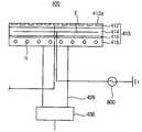
도 1을 참조하면, 본 발명의 일실시예에 의한 물리기상증착 장치(1000)는 기판(w) 상에 상변화 물질을 증착하는 공정챔버(100), 상기 상변화 물질의 이온입자를 공급하는 타겟(200), 플라즈마 상태의 공정가스를 생성하는 플라즈마 발생부(300), 증착공정이 진행되는 동안 상기 기판(w)을 고정하는 기판 지지부(400) 및 증착공정이 진행되는 동안 선택적으로 기판의 주변부로 복사열을 공급하는 보조열원(600)을 포함한다.Referring to FIG. 1, a physical
상기 공정챔버(100)는 상변화 물질에 대한 증착공정이 진행되는 동안 외부로부터 밀폐되고 고온 고압의 상태로 유지된다. 본 실시예의 경우, 상기 공정챔버(100)는 증착공정이 수행되는 증착 챔버(120) 및 상기 증착챔버(120)와 연통되도록 증착챔버(120)의 하부에 배치되고 증착대상 기판(w)이 로딩되는 로딩 챔버(140)를 구비한다. 상기 로딩 챔버(140)는 물리기상증착 장치(1000)의 하우징과 일체로 제공된다.The
상기 증착챔버(120)는 소정의 크기를 갖는 제2 공간(S2)을 한정하는 측벽과 바닥면으로 구성되고 바닥면에는 하부의 로딩 챔버(140)와 연통하는 챔버 연통 개구(122)가 배치된다. 상기 챔버 연통 개구(122)를 통하여 상기기판(w)을 지지하는 기판 지지부(400)가 증착챔버(120)와 로딩챔버(140) 사이에서 이동한다.The
증착챔버(120)의 상부는 상변화 물질을 구비하는 타겟(200)과 공정가스를 플라즈마 상태로 여기(exciting)하는 플라즈마 발생부(300)가 배치된다. 따라서, 상기 제2 공간(S2)은 측벽 및 상기 챔버 연통 개구(122)를 구비하는 바닥면과 상기 타겟 및/또는 플라즈마 발생부(300)에 의해 한정된다.In the upper part of the
상기 증착챔버(120)의 측부에는 상기 제2 공간(S2)으로 공정가스를 공급하는 공정가스 공급부(810)가 배치된다. 가스 저장탱크(T)에 저장된 공정가스는 공급관로(811)와 공급밸브(812)를 통하여 상기 제2 공간(S2)으로 공급되고, 후술하는 플라즈마 발생부(300)에 의해 인가되는 전력에 의해 플라즈마 상태로 여기된다.A process
또한, 도시되지는 않았지만, 상기 증착챔버(120)의 측벽에는 펌프와 결합된 배기관(도시되지 않음)이 배치된다. 펌프에 의해 증착챔버(120)의 내부는 공정에 적합한 압력으로 유지되고 증착챔버(120)의 내부에서 발생되는 공정부산물은 배기관을 통해 외부로 배출될 수 있다. 본 실시예의 경우, 상기 증착챔버(120)는 증착공정이 진행되는 동안 약 13mTorr 내지 75mTorr, 바람직하게는 약 40mTorr 내지 75mTorr의 압력으로 유지될 수 있다.Further, although not shown, an exhaust pipe (not shown) associated with the pump is disposed on the side wall of the
상기 로딩 챔버(140)는 제1 공간(S1)을 한정하는 벽체와 바닥면을 구비하고 상부는 챔버 연통 개구(122)를 구비하는 증착챔버(120)의 바닥면에 의해 한정된다. 로딩 챔버(140)의 벽체와 바닥면은 상기 공정챔버(100)의 외곽을 한정하는 하우징으로 기능한다.The
로딩 챔버(140)의 측벽은 부분적으로 개구되어 증착대상 기판을 로딩하는 게이트(142)가 제공되고 바닥면은 후술하는 기판 지지부(400)의 회전축(420)가 관통하도록 관통 개구를 구비한다.The side wall of the
이에 따라, 증착챔버(120)는 공정챔버(100)의 하우징에 의해 한정되는 내부 공간의 상부에 배치되어 외부와 충분히 밀폐되어 물리기상증착 공정이 진행되고 로딩 챔버(140)는 증착 챔버(120)의 하부에 배치되는 공정챔버(100) 하우징의 하부로서 증착대상 기판(w)을 수용하여 증착공정을 준비한다.Accordingly, the
상기 타겟(target, 200)은 증착챔버(120)의 상부에 배치되어 제2 공간(S2)을 한정하고 공정가스의 플라즈마와 반응하여 증착물질의 이온입자를 생성한다. 본 실시예의 경우, 상기 증착물질은 기화열이 낮은 상변화 물질을 포함한다. 예를 들면, 상기 타겟(200)은 게르마늄(germanium, Ge), 텔루륨(tellurium, Te) 및 안티몬(antimony, Sb)을 함유하는 화합물(compound)로 이루어진다. 그러나, 상변화 물질뿐만 아니라 기화열이 낮은 물질을 플라즈마를 이용하여 기판에 증착하는 경우라면 상술한 바와 같은 상변화 물질뿐만 아니라 다양한 종류의 증착물질이 상기 타겟(200)에 제공될 수 있음은 자명하다. 타겟(200)은 기판(W)과 유사한 크기 및 형상을 가지며 기판 지지부(400)에 놓여진 웨이퍼(W)와 대향되도록 배치된다.The
상기 타겟(200)은 증착챔버(120)로 공급된 공정가스를 플라즈마 상태로 여기하는 플라즈마 발생부(300)와 연결된다. 상기 플라즈마 발생부(300)는 타겟(200)에 고주파 교류전력을 인가하는 제1 전력 공급부(320)와 직류전력을 인가하는 제2 전력 공급부(340)를 구비한다. 상기 제1 전력 공급부(320)에 인가된 플라즈마 임피던스는 정합기(matching device, 560)에 의해 전송로 임피던스(transmission path impedance)로 정합되어 상기 타겟(200)과 연결된 상부전극(미도시)으로 공급된다. 예를 들면, 상기 제1 전력 공급부(320)는 약 60MHz 내지 100MHz의 주파수를 갖고 약 5KW 내지 10KW의 고주파 전력을 공급하고, 상기 제2 전력 공급부(340)는 약 6KW 내지 12KW의 직류전력을 공급할 수 있다.예를 들면, 상기 공정 가스는 헬륨이나 아르곤과 같은 불활성 기체를 포함한다.The
상기 공정가스의 플라즈마는 상기 타겟(200)으로부터 증착물질을 이온입자의 형태로 분리한다. 분리된 이온입자는 후술하는 기판 지지부의 내부에 배치된 하부전극(E)으로 유도되어 기판(w)에 증착된다.The plasma of the process gas separates the deposition material from the
상기 기판 지지부(400)는 상하로 수직 이동되고 회전 가능하게 구성된다. 상기 로드 챔버(140)의 대기 위치에 기판 지지부(400)가 위치하면, 게이트(142)를 통하여 증착대상 기판(w)이 로딩되어 상면에 고정된다. 기판이 고정되면, 상기 기판 지지부(400)는 상방으로 이동하여 증착챔버(120)의 내부로 수직 상승한다. 증착챔버(120)의 내부에서 증착공정이 완료되면, 기판 지지부(400)는 하강하여 대기 위치에 위치하고 증착이 완료된 기판은 상기 게이트(142)를 통하여 외부로 언로딩된다.The
도 2는 도 1에 도시된 기판 지지부를 상세하게 나타내는 도면이다.FIG. 2 is a detailed view of the substrate support shown in FIG. 1. FIG.
도 2를 참조하면, 상기 기판 지지부(400)는 상기 기판(w)이 고정되는 고정판(410), 상기 고정판(410)과 연결되어 상기 고정판을 이동하고 회전시키는 연결축(420) 및 상기 연결축(40)을 구동하는 구동부(430)를 포함한다.2, the
상기 고정판(410)은 상기 기판(w)과 접촉하는 제1 평판(412), 상기 하부전극(E)이 배치되는 제2 평판(414) 및 상기 히터(H)가 배치된 제3 평판(418)을 포함한다. 선택적으로, 상기 제2 평판(414)과 제3 평판(416) 사이에 배치되어 상기 히터(H)로부터 발생한 열을 효과적으로 기판(W)으로 전달하기 위한 시트 구조물(416)을 더 구비할 수 있다.The fixing
제1 평판(412)의 표면에는 다수의 홈(412a)이 배치되어 상기 제2 공간(S2)으로 공급된 공정가스 및 반응 부산물을 제거할 수 있는 배출경로(discharge path)로 제공된다. 상기 홈(412a)으로 수집된 공정가스 및 반응 부산물은 배출관(440)을 통하여 상기 공정챔버(100)의 외부로 배출된다. 선택적으로, 상기 배출가스는 재생기(R)에 의해 정화되어 상기 가스 저장탱크(T)로 재공급될 수 있다.A plurality of
상기 히터(H)는 제3 평판(418)의 내부에 일정한 간격으로 배치되어 증착공정이 진행되는 동안 제1 평판(412) 상에 고정된 기판이 일정한 온도를 유지하도록 열을 제공한다. 예를 들면, 상기 히터(H)는 코일형상의 열선을 구비하여 주울열이 기판으로 제공될 수 있다.The heaters H are arranged at regular intervals in the third
이때, 상기 제3 평판(418)의 주변부에 배치된 히터에서 발산되는 열은 상기 기판 지지부(400)의 측부를 통하여 상기 제2 공간(S2)으로 발산되어 중심부에 배치된 히터로부터 발생된 열과 비교하여 기판(w)을 가열하는 열량이 상대적으로 작아지게 된다. 이에 따라, 상기 기판(w)은 중심부 온도는 높고 주변부 온도는 낮게 형성된다.At this time, the heat emitted from the heater disposed at the peripheral portion of the third
기판의 중심부와 주변부의 온도편차가 발생하는 경우, 기화열이 낮은 증착물질을 높은 온도에서 증착하게 되면, 증착물질의 기화정도(degree of vaporization)가 기판의 중심부와 주변부에서 상이하게 되므로 증착되는 막질의 조성과 두께가 불균일하게 형성된다.When a temperature deviation occurs between the central portion and the peripheral portion of the substrate, if the deposition material having a low vaporization heat is deposited at a high temperature, the degree of vaporization of the deposition material is different between the central portion and the peripheral portion of the substrate, The composition and thickness are unevenly formed.
그러나, 후술하는 바와 같이, 증착온도와 비교하여 기화열이 낮은 증착물질을 증착하는 경우 상기 기판의 주변부를 둘러싸는 보조열원(600)을 통하여 기판(w)의 주변부로 추가적인 복사열을 제공함으로써 기판의 표면온도 산포를 균일하게 유지함으로써 증착물질의 기화도를 균일하게 조정할 수 있다. 이에 따라, 기화열이 작은 증착물질을 고온에서 증착한다 할지라도 기판의 표면에 균일한 박막을 형성할 수 있다.However, as described later, when depositing a vapor deposition material having a low vaporization heat as compared with the deposition temperature, additional heat is radiated to the peripheral portion of the substrate w through the
상기 하부전극(E)은 타겟(200)으로부터 방출된 증착물질의 이온입자들을 기판(W)과 수직한 방향으로 유도한다. 예를 들면, 상기 하부전극(E)은 상기 제2 평판(514)의 내부에 매립된 적어도 하나의 전극을 포함하고, 상기 플라즈마 발생부(300)에 구비된 상부전극과 서로 대향하도록 배치된다. 이에 따라, 상기 이온입자는 상부전극과 하부전극 사이에 형성되는 전기장에 의해 기판(w)의 표면으로 유도된다.The lower electrode E induces ion particles of the deposition material emitted from the
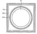
이때, 상기 이온입자들이 기판(w)의 표면을 향하여 수직하게 입사될 수 있도록 상기 타겟(200)의 상부에 자성체(500)를 더 배치할 수 있다. 상기 자성체(500)는 디스크 형상을 갖고 제1 극성을 갖고 중심부에 배치되는 제1 자성체(520)와 제1 극성과 다른 제2 극성을 갖고 주변부에 배치되어 제1 자성체(520)를 둘러싸는 제2 자성체(540)를 구비한다. 공정이 진행되는 동안, 상기 자성체(500)는 디스크의 중심축을 중심으로 일정한 각속도로 회전함으로써 자기장의 영역을 주기적으로 변경한다.At this time, the
이에 따라, 자성체(500)에 의해 형성되는 자기장은 기판(w)의 주변부보다는 타겟(200)의 주변부에서 밀도가 높게 형성되어 상기 이온 입자들이 기판(w)에 수직하게 입사하여 증착 균일도를 높일 수 있다. 또한, 상기 자성체(500)의 회전에 의해 상기 이온입자들을 생성하는 타겟(200)의 부식을 균일하게 수행할 수 있다.Accordingly, the magnetic field formed by the
타겟(200)으로부터 생성된 증착물질의 이온입자들은 상부전극 및 하부전극(E) 사이에 형성되는 전기장에 의해 상기 기판(E)으로 유도되어 기판(w)의 상면에 증착된다.The ion particles of the deposition material generated from the
종횡비가 큰 개구 또는 리세스를 구비하는 구조물이 상기 기판(w) 상에 형성되고, 물리기상증착 공정에 의해 상기 개구나 리세스를 매립하는 경우 매립(gap-fill) 특성을 높이기 위해 상기 물리기상증착 공정은 충분히 높은 온도에서 수행된다. 상기 히터(H)로 기판(w)을 가열하여 공정온도를 높이게 되면 상술한 바와 같이 기판(w)의 중앙부와 주변부의 온도편차도 함께 증가한다. 이에 따라, 증착되는 기화열의 정도에 따라 기판의 중앙부와 주변부에서 기화정도(휘발정도)가 서로 상이하게 되어 기판 상에 형성되는 박막의 조성과 두께에 차이를 유발한다.A structure having an opening or recess having a large aspect ratio is formed on the substrate w and the physical vapor deposition process is performed to increase the gap-fill characteristic when the opening or the recess is buried by the physical vapor deposition process, The deposition process is performed at sufficiently high temperatures. When the process temperature is increased by heating the substrate W with the heater H, the temperature deviation between the central portion and the peripheral portion of the substrate w also increases as described above. Accordingly, the degree of vaporization (degree of volatilization) at the central portion and the peripheral portion of the substrate are different from each other depending on the degree of vaporization of the deposited vapor, thereby causing a difference in the composition and thickness of the thin film formed on the substrate.
특히, 게르마늄(germanium; Ge), 텔루륨(tellurium; Te), 안티몬(antimony; Sb)로 구성되는 다층막을 이용하여 상변화 메모리 소자의 데이터 저장부를 형성하는 경우, 매립 특성을 개선하기 위해 증착온도를 높이는 경우 상기 구성물질들의 낮은 기화열로 인하여 기판의 중심부와 주변부에서 데이터 저장부를 구성하는 박막의 두께와 조성의 산포가 크게 발생한다.Particularly, when a data storage portion of a phase change memory device is formed using a multilayer film composed of germanium (Ge), tellurium (Te), and antimony (Sb) The thickness and the composition of the thin film constituting the data storage part are greatly scattered in the central part and the peripheral part of the substrate due to the low vaporization heat of the constituent materials.
기판의 주변부와 중심부에서의 상변화 물질막의 균일도를 높일 수 있도록 기판의 주변부로 복사열을 추가적으로 공급하는 보조열원(610)이 배치된다. 이때, 상기 보조열원(610)은 상기 공정챔버(100)의 내부에서 다양하게 배치될 수 있다. 상기 로딩 챔버(140)의 내부에 배치되어 기판 지지부(400)의 하부에서 기판(w) 주변부를 가열할 수도 있고, 상기 증착챔버(120)의 내부에 배치되어 기판 지지부(400)의 상부에서 기판 주변부를 가열할 수도 있다.An
도 3a는 본 발명의 일실시예에 의한 보조열원을 나타내는 단면도이고, 도 3b는 도 3a에 도시된 보조열원을 나타내는 평면도이다.FIG. 3A is a cross-sectional view showing an auxiliary heat source according to an embodiment of the present invention, and FIG. 3B is a plan view showing the auxiliary heat source shown in FIG. 3A.
도 3a 및 도 3b를 참조하면, 상기 보조열원(610)은 상기 로딩 챔버(140)의 내부에 배치되어 상기 기판 지지부(400)의 바닥면 주변부로부터 이격되어 배치된다. 예를 들면, 상기 보조열원(610)은 상기 기판 지지부(400)를 둘러싸도록 링 형상을 갖는 전열 램프(electrical heating lamp)를 포함한다. 이와 달리, 상기 보조열원(610)은 상기 기판 지지부(400)를 둘러싸는 링 형상을 갖는 고온 유체공급 튜브(fluid flow tube)로 제공될 수 있다.3A and 3B, the
상기 보조열원(610)은 기판 지지부(400)의 하부에서 기판의 주변부를 따라 배치되므로 상기 보조열원(610)으로부터 공급되는 열은 복사에 의해 상기 기판(w)의 주변부로 전달된다. 특히, 상기 보조열원(610)은 기판 지지부(400)의 주변부로부터 일정한 거리만큼 이격되어 제3 평판(412)의 하부에 배치된다. 예를 들면, 상기 보조열원은 제3 평판(418)의 에지라인으로부터 수평방향으로 약 5-10cm 정도로 이격된 후 상기 제3 평판(418)의 하부에 배치된다. 이에 따라, 상기 보조열원에 의해 상기 기판 지지부(400)를 가열하는 것이 아니라 복사에 의해 기판(w)의 주변부를 직접 가열하게 된다. 뿐만 아니라, 상기 증착 챔버(120)의 측벽 및 바닥면을 가열함으로써 제2 공간(S2)의 내부온도를 상승시켜 간접적으로 기판 주변부의 온도를 상승시키는 효과도 달성할 수 있다.Since the
선택적으로, 상기 로드 챔버(140)의 내측벽 및 바닥면을 따라 배치되고 상기 제1 공간(S1)을 향하여 오목하게 배치되는 열차단 부재(620)가 더 배치될 수 있다. 상기 보조열원(610)에서 생성되는 열은 사방으로 방사되므로 기판 지지부(400)를 향하여 방사될 뿐만 아니라 로드 챔버(140)의 내측벽 및 바닥면 방향으로도 방사된다. 로드 챔버(140)의 내측면 및 바닥면으로 방사되는 열은 로드 챔버(140)의 외부로 손실되어 상기 기판(w)을 가열하는 열원으로 기능할 수 없게 된다. 이에 따라, 로드 챔버(140)의 내측면 바닥면을 따라 열차단 부재(620)를 배치하여 외부로 열이 손실되는 것을 방지한다.Optionally, a
특히, 열차단 부재(620)의 방사면을 상기 기판(w)을 향하도록 오목하게 형성함으로써 상기 제1 공간(S1)의 전체 온도를 효율적으로 상승시킬 수 있다. 이때, 상기 게이트(142)에 대응하는 관통 홀(621)이 배치되어 기판(w)의 로딩 및 언로딩시 상기 기판(w)이 열차단 부재(620)를 관통할 수 있다.Particularly, the entire temperature of the first space S1 can be efficiently raised by forming the radiation surface of the
상기 보조열원(610)은 다양한 형상으로 변형될 수 있다.The
도 4a 및 도 4b는 도 3b에 도시된 보조열원의 변형례를 나타내는 도면이다.4A and 4B are views showing a modification of the auxiliary heat source shown in FIG. 3B.
도 4a에 도시된 바와 같이 상기 보조열원(610)은 상기 기판 지지부(400)를 둘러싸는 보조 척(610b)과 상기 보조척(610b)의 내부에 매립된 전열 히터(610b)로 구성될 수 있다. 이에 따라, 상기 기판(w)이 로딩 및 언로딩되는 과정에서 발생하는 외란으로부터 전열히터(610b)를 보호하여 보조열원을 안정적으로 배치할 수 있다.4A, the
이와 달리, 도 4b에 도시된 바와 같이 상기 보조열원(610)은 상기 기판 지지부(400) 주변을 웨이브 형태로 둘러싸는 굴곡 전열라인(610b)으로 형성할 수도 있다. 상기 제2 공간(S2)에 배치되는 구조물들의 특성과 구조에 의해 기판 지지부(400)로부터 일정한 거리만큼 이격되는 전열선을 배치하는 것이 용이하지 않은 경우 내부 구조물들과의 간섭을 방지할 수 있도록 웨이브 형상의 굴곡 전열라인(610b)으로 배치할 수도 있다. 이때, 상기 굴곡 전열라인(610b)의 만곡부를 상기 기판 지지부(400)로부터 약 5-10cm 이격되도록 배치한다.Alternatively, as shown in FIG. 4B, the
도 5a는 본 발명의 다른 실시예에 의한 보조열원을 나타내는 단면도이고, 도 5b는 도 5a에 도시된 보조열원을 나타내는 평면도이다.FIG. 5A is a cross-sectional view showing an auxiliary heat source according to another embodiment of the present invention, and FIG. 5B is a plan view showing the auxiliary heat source shown in FIG. 5A.
도 5a 및 도 5b를 참조하면, 상기 보조열원(610)은 상기 증착 챔버(120)의 내부에 배치되어 상기 기판 지지부(400)의 상면 주변부로부터 이격되어 배치된다.5A and 5B, the
이때, 상기 보조열원(610)은 상기 기판 지지부(400)의 제1 평판(412)를 둘러싸는 링 형상의 전열 램프를 포함한다. 상기 전열램프(610)는 증착챔버(120)의 바닥면 상에 배치될 수도 있고 바닥면 및 측벽으로부터 이격되어 상기 제2 공간(S2)에 배치될 수도 있다. 상기 전열램프(610)는 제1 평판(412)으로부터 약 5-10cm 이격되어 상기 제1 평판(412)을 둘러싸도록 배치되므로 상기 전열램프(610)로부터 방사되는 열은 제1 평판(412)을 직접 가열하는 것이 아니라 복사에 의해 상기 기판(w)의 주변부 온도를 상승시키게 된다. 이에 따라, 기판의 주변부와 중심부의 온도편차를 줄일 수 있다.At this time, the
본 실시예의 경우, 상기 증착챔버(120)의 내부에 배치되는 보조열원(610)은 전열램프만을 개시하고 있지만, 증착챔버의 공정조건에서 고온의 유체를 전송할 수 있는 튜브를 구성할 수 있다면 유체 공급튜브도 배치할 수 있음은 자명하다.In the case of this embodiment, the
또한, 로드 챔버(140)에서와 마찬가지로 상기 증착챔버(120)의 내측면 및 바닥면을 따라 열차단 부재(620)가 선택적으로 구비될 수 있다. 상기 열차단 부재(620)는 증착 챔버(120)의 측벽 및 바닥면과 연결되고 상기 제2 공간(S2)을 향하도록 오목하게 배치되어 상기 보조열원(610)으로부터 발산하는 열이 상기 증착 챔버(120)의 외부로 소실되는 것을 방지하고 상기 제2 공간(S2)의 내부온도를 상승시킨다.Also, as in the case of the
특히, 제2 공간(S2)의 전체적인 내부온도를 상승시키는 경우, 기판에 증착되는 과정에서 증발된 증착물질이 증착챔버(120)의 상부 측벽에 증착되는 것을 방지할 수 있다.In particular, when the overall internal temperature of the second space S2 is raised, it is possible to prevent evaporated deposition material from being deposited on the upper sidewall of the
종래의 PVD 장치에 의하면, 기판이 고정되는 제1 평판(412)에는 상기 히터(H)로부터 지속적으로 열이 공급되므로 증착챔버(120)의 하부는 상부와 비교하여 상대적으로 높은 온도를 유지한다. 따라서, 기화열이 낮은 상변화 물질이 기판 주변에서 증발하는 경우, 상대적으로 온도가 낮은 증착챔버의 상부에서 증발된 증착물질이 석출되거나 플라즈마에 의한 반응 부산물이 측벽에 증착될 수 있다.According to the conventional PVD apparatus, since the heat is continuously supplied from the heater H to the first
그러나, 본 발명에 의한 PVD 장치에 의하면, 보조열원(610)과 열차단 부재(620)에 의해 상기 제2 공간(S2)의 전체적인 내부온도가 상승하므로 증발된 상변화 물질이나 반응 부산물이 증착챔버의 상부측벽에 증착되는 것을 방지할 수 있다. 이에 따라, 상기 PVD 장치의 수선과 교체주기를 증가시킴으로써 장비의 유지비용을 낮출 수 있다.However, according to the PVD apparatus of the present invention, since the overall internal temperature of the second space S2 rises by the
도 6a는 본 발명의 또 다른 실시예에 의한 보조열원을 나타내는 단면도이고, 도 6b는 도 6a에 도시된 보조열원을 나타내는 평면도이다.FIG. 6A is a cross-sectional view showing an auxiliary heat source according to another embodiment of the present invention, and FIG. 6B is a plan view showing the auxiliary heat source shown in FIG. 6A.
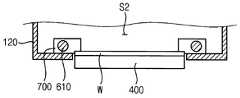
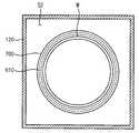
도 6a 및 도 6b를 참조하면, 상기 증착챔버(120)의 바닥면에 고정되어 상기 기판(w)을 상기 기판 지지부(400)에 고정하는 고정부재(700)를 더 포함하고, 상기 보조열원(610)은 상기 고정부재(700)의 내부에 배치되는 전열기구(electrical heating body)를 포함할 수 있다.6A and 6B, the apparatus further includes a fixing
상기 고정부재(700)는 증착공정이 진행되는 동안 기판(W)이 기판 지지부(400)로부터 이탈되지 않도록 기판(W)을 고정한다. 이때, 상기 고정부재(700)는 기계적으로 기판(w)을 제1 평판(412)에 고정한다. 예를 들면, 상기 고정부재(700)는 증착챔버(120)의 바닥면에 고정되고 타단은 기판(w)의 상면과 접촉하는 디스크 형상으로 제공된다. 이에 따라, 고정부재(700)에 의해 기판(w)으로 인가되는 기계적 외력에 의해 제1 평판(412)과 기판(w)을 고정한다. 상기 기계적 외력은 고정부재(700) 자체의 탄성력이나 일정한 힘으로 인가되는 압축력일 수 있다.The fixing
이때, 상기 보조열원(610)은 상기 고정부재(700)의 내부에 매립되어 상기 기판(w)의 둘레를 링 형상으로 둘러싸도록 배치된다. 예를 들면, 상기 보조열원(610)은 상기 제1 평판(412)으로부터 약 5-10cm 이격된 채 제1 평판(412)의 주변부를 따라 배치될 수 있다. 이에 따라, 증착챔버(120) 내부의 증착공정 환경으로부터 상기 보조열원(610)을 보호할 수 있다.At this time, the
상기 공정챔버(100)의 주변부에는 상기 보조열원(610)으로 열을 공급하는 열 공급부(820) 및 상기 히터(H)와 하부전극(E)으로 전원을 공급하는 전원 공급부(830)가 배치된다.A
상기 열 공급부(820)는 상기 보조열원(610)과 전기적 또는 기계적 방법으로 연결되어 상기 보조열원으로 열을 공급한다. 예를 들면, 상기 열 공급부(820)는 전열라인으로 전원을 공급하는 전원이나 유체공급 튜브로 고온의 유체를 공급하는 고온유체 저장부로 구성될 수 있다.The
상기 전원 공급부(830)는 상기 히터(H)를 가열하기 위한 직류전원이나 상기 하부전극(E)에 RF 전력을 공급하기 위한 교류전원을 구비할 수 있다. 예를 들면, 상기 전원 공급부(830)는 약 13.56MHz의 주파수로 1KW의 전력을 공급할 수 있다.The
상기 공정가스 공급부(810), 상기 플라즈마 발생부(300), 상기 열공급부(820)원 및 상기 전원 공급부(830)와 연결되어 상기 공정챔버(100) 내부에서 상기 상변화 물질막을 형성하는 물리기상 증착공정을 제어하는 제어부(900)를 더 구비한다.A physical vapor deposition (CVD) process, which is connected to the process
상기 기판 지지부(400)로의 기판(w) 로딩 및 언로딩, 히터(H) 구동에 의한 기판의 가열 및 플라즈마의 생성, 상부전극과 하부전극 사이에 전기장 및 자기장의 설정 및 상변화 물질 이온입자의 기판으로의 유도는 상기 제어부(900)에 의해 제어되어 상기 기판(w) 상에 상변화 물질막이 형성된다.Heating and heating the substrate by driving the heater H, setting the electric field and the magnetic field between the upper electrode and the lower electrode, setting the electric field and the magnetic field between the upper electrode and the lower electrode, The induction to the substrate is controlled by the
이때, 증착되는 상기 상변화 물질의 기화열이 일정한 설정값 이하로 판단되면, 상기 제어부(900)는 열공급부(820)를 구동하여 상기 보조열원(610)을 통하여 복사열을 공급한다. 이에 따라, 상기 기판(w)의 주변부와 중심부의 온도편차에 의해 상변화 물질의 증착두께가 달라지는 것을 방지함으로써 기판(w)의 상면에 형성되는 상변화 물질막의 조성과 두께의 편차를 줄이고 균일도를 높일 수 있다.At this time, if it is determined that the vaporization heat of the phase change material to be deposited is lower than a predetermined set value, the
뿐만 아니라, 상기 보조열원(610)을 통하여 공급하는 복사열의 양을 조절함으로써 제2 공간(S2)의 내부온도를 제어할 수 있다. 제2 공간(S2)의 내부온도가 높을 경우 상변화 물질의 기화를 촉진하여 기판에 형성되는 상변화 물질막의 두께를 줄일 수 있고, 내부온도를 일정온도 이하로 억제하는 경우 상변화 물질의 기화를 억제함으로써 기판에 형성되는 상변화 물질막의 두께를 증가시킬 수 있다.In addition, the internal temperature of the second space S2 can be controlled by adjusting the amount of the radiant heat supplied through the
또한, 특정한 물질의 기화열을 중심으로 상기 제2 공간(S2)의 내부온도를 조절함으로써 특정물질의 증착량을 높이거나 낮출 수 있다. 이에 따라, 기판(w)에 증착되는 상변화 물질막의 조성을 제어할 수도 있다.In addition, the deposition amount of a specific substance can be increased or decreased by adjusting the internal temperature of the second space S2 around the heat of vaporization of a specific substance. Thus, the composition of the phase change material film deposited on the substrate w may be controlled.
본 실시예의 경우, 상기 제어부(900)는 상기 상변화 물질의 기화열이 약 200mJ 이하인 경우에 상기 보조열원(610)을 구동하여 상기 제2 공간(S2)의 내부온도를 약 200℃ 내지 약 500℃로 유지한다.
In the present embodiment, the
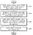
도 7은 본 발명의 일실시예에 따라 도 1에 도시된 물리기상증착장치를 이용하여 기판 상에 상변화 물질막을 형성하는 방법을 나타내는 흐름도이다. 도 8은 본 발명의 일실시예에 따라 도 7에 도시된 물리기상증착 공정을 준비하는 단계를 나타내는 흐름도이다.7 is a flowchart illustrating a method of forming a phase change material layer on a substrate using the physical vapor deposition apparatus shown in FIG. 1 according to an embodiment of the present invention. FIG. 8 is a flow chart illustrating a step of preparing the physical vapor deposition process shown in FIG. 7 according to an embodiment of the present invention.
도 1, 도 7 및 도 8을 참조하면, 상변화 물질을 구비하는 타겟(200)이 배치된 증착챔버(120)의 내부에 기판(w)을 배치하고 물리기상증착 공정을 준비한다(단계 S100).1, 7 and 8, a substrate w is disposed in a
예를 들면, 상기 증착챔버(120)의 하부에 배치된 로딩챔버(140)로 상기 기판(w)을 로딩시켜 히터(H)와 전극(E)을 구비하는 기판 지지부(400)에 상기 기판(w)을 고정한다(단계 S110).For example, the substrate W is loaded onto a
로봇 암과 같은 이송수단을 이용하여 풉(미도시)으로부터 증착대상 기판을 반출하고 상기 게이트(142)를 통하여 제1 평판(412)의 상면에 위치시킨다.The substrate to be deposited is taken out of the FOUP (not shown) using a transferring means such as a robot arm, and is positioned on the upper surface of the first
이어서, 상기 기판(w)이 고정된 상기 기판 지지부(400)를 상기 증착챔버(120)로 상승시켜 제 공간(S2)에 상기 기판(w)을 위치시킨다(단계 S120). 상기 구동부(430)에 의해 회전축(420)을 상승시켜 상기 고정판(410)을 증착챔버(120)의 내부공간인 제2 공간(S2)에 배치하고, 상기 회전축(420)을 회전시켜 기판을 정렬시킨다. 이어서, 상기 고정부(700)를 이용하여 기판(w)을 고정판(410)에 고정한다.Subsequently, the
이어서, 상기 히터(H)를 구동하여 상기 기판(w)을 가열(단계 S130)하고, 상기 증착챔버(120)의 내부압력 및 내부온도를 상변화 물질의 증착조건에 따라 예비적으로 조절한다(S140).Subsequently, the heater H is driven to heat the substrate w (step S130), and the internal pressure and the internal temperature of the
예를 들면, 증착 챔버(120)에 구비된 펌프를 구동하여 공정압력으로 미리 설정하고 공정가스를 플라즈마 반응을 준비할 수 있는 온도로 상기 제2 공간(S2)의 내부온도를 설정할 수 있다. 본 실시예의 경우, 상기 증착챔버(120)는 증착공정이 진행되는 동안 약 13mTorr 내지 75mTorr의 압력으로 유지될 수 있도록 조절된다.For example, the pump provided in the
이어서, 상기 증착챔버(120)의 내부로 공급된 공정가스를 플라즈마 상태로 여기하여, 상기 타겟(200)으로부터 상기 상변화 물질의 이온입자를 생성한다(단계 S200). 상기 플라즈마 발생부(300)를 구동하여 고주파 전력을 공급하여 제2 공간(S2)으로 공급된 공정가스를 플라즈마 상태로 여기한다. 플라즈마 상태의 공정가스는 상변화 물질을 구비하는 상기 타겟(200)으로부터 상변화 물질을 이온입자의 형태로 분리한다. 이때, 상기 자성체(500)도 함께 구동하여 상기 타겟(200)의 주변부에 충분한 세기의 자기장을 형성하여 생성된 이온입자들이 타겟(200)의 주변부에 집중적으로 분포하도록 조절한다. 또한, 상기 자성체(500)를 회전시킴으로써 상변화 물질의 이온입자들이 타겟(200)의 모든 영역으로부터 균일하게 생성될 수 있도록 한다.Subsequently, the process gas supplied into the
이때, 상기 상변화 물질의 물성과 상기 증착챔버(120) 내부의 공정조건에 따라 선택적으로 보조열원(610)을 구동하여 상기 기판(w)의 주변부로 선택적인 복사열을 공급하고(단계 S300), 상기 상부전극과 하부전극(E) 사이에 전기장을 형성하여 상기 상변화 물질의 이온입자를 상기 기판(w)으로 유도한다(단계 S400).At this time, the
예를 들면, 상기 상변화 물질막이 게르마늄(Ge)-안티몬(Sb)-텔루륨(Te) 복합막(GST 막)인 경우, 게르마늄(Ge)과 텔루륨(Te)의 기화열이 안티몬(Sb)과 비교하여 상대적으로 낮으므로 기판의 주변부와 중심부의 온도편차가 발생할 경우 게르마늄(Ge)과 텔루륨(Te)의 증착량이 기판의 주변부와 중심부에서 상이할 수 있다. 이에 따라, 기판의 주변부에 형성되는 GST 막과 중심부에 형성되는 GST막의 조성과 두께가 상이할 수 있다.For example, when the phase change material film is a germanium (Ge) -antimony (Sb) -Teruium (Te) composite film (GST film), the heat of vaporization of germanium (Ge) and tellurium (Te) The deposition amount of germanium (Ge) and tellurium (Te) may be different from each other in the peripheral portion and the central portion of the substrate when the temperature deviation occurs between the peripheral portion and the central portion of the substrate. Accordingly, the composition and thickness of the GST film formed in the peripheral portion of the substrate and the GST film formed in the central portion may be different from each other.
한편, 상변화 메모리 소자의 집적도가 증가함에 따라 상변화 메모리 소자의 게이트 전극으로 이용되는 상기 GST 막이 형성되는 홀(hole)의 종횡비도 증가하고 이에 따라 GST 막의 매립특성을 높이기 위하여 고온에서 증착공정이 수행되는 경우가 증가하고 있다.As the degree of integration of the phase change memory device increases, the aspect ratio of the hole in which the GST film used as the gate electrode of the phase-change memory device is formed increases. Thus, in order to improve the filling property of the GST film, Is increasing.
이에 따라, 상변화 메모리 소자의 게이트 전극을 형성하는 경우, 상기 상변화 물질의 낮은 기화열과 상대적으로 높은 증착온도에 의해 기판의 주변부에 형성되는 칩의 게이트 전극과 주변부에 형성되는 게이트 전극의 조성과 두께가 상이하게 형성될 수 있다.Thus, in the case of forming the gate electrode of the phase change memory element, the composition of the gate electrode formed in the periphery of the chip and the gate electrode formed in the periphery of the substrate by the low vaporization heat of the phase change material and the relatively high deposition temperature The thickness may be different.
상기 제어부(900)는 증착되는 물질의 기화열이 설정값 이하이고 증착챔버(120)의 공정온도가 설정온도 이상인 경우, 상기 보조열원(610)을 구동하여 기판의 주변부로 추가적인 복사열을 공급한다. 이에 따라, 기판의 주변부와 중심부의 온도편차를 줄이고 주변부와 중심부에 증착되는 물질의 증착량을 균일하게 유지할 수 있다.The
뿐만 아니라, 상기 보조열원(610)을 통하여 공급하는 복사열의 양을 조절함으로써 제2 공간(S2)의 내부온도를 제어하고 이에 따라 상기 GST 막의 조성과 두께를 조절할 수도 있다.In addition, the inner temperature of the second space S2 may be controlled by adjusting the amount of the radiant heat supplied through the
본 실시예의 경우, 상기 제어부(900)는 상기 상변화 물질의 기화열이 약 200mJ 이하인 경우에 상기 보조열원(610)을 구동하여 상기 제2 공간(S2)의 내부온도를 약 200℃ 내지 약 500℃로 유지한다. 그러나, 증착되는 물질의 기화열의 편차에 따라 적정한 값으로 보조열원의 구동 기준값을 설정할 수 있음은 자명하다.In the present embodiment, the
이때, 상기 보조열원(610)이 전열라인으로 구성되는 경우에는 상기 열 공급부(820)의 전원을 선택적으로 온/오프 시킴으로써 보조열원의 구동을 제어할 수 있다. 이에 따라, 상기 기판 지지부(400)를 둘러싸는 링 타입의 보조열원(610)은 주울열을 발생할 수 있다.At this time, when the
이와 달리, 상기 보조열원(610)이 고온 유체공급 튜브로 구성되는 경우에는 상기 열 공급부(820)의 유량 제어밸브를 선택적으로 개폐시킴으로써 보조열원의 구동을 제어할 수 있다. 이에 따라, 상기 기판 지지부(400)를 둘러싸는 링 타입의 보조열원(610)은 상기 튜브로 공급된 고온유체에 저장된 열을 발생할 수 있다.Alternatively, when the
본 발명의 일실시예에 의한 물리기상증착장치 및 이를 이용한 상변화 물질막의 증착방법에 의하면, 증착공정이 진행되는 동안 증착물질의 기화열이 작고 증착온도가 높은 경우 기판의 주변부로 복사열을 추가적으로 공급하여 기판의 주변부와 중앙부의 온도편차에 의한 증착량이 변화를 최소화할 수 있다. 이에 따라, 기판의 주변부와 중앙부에서 증착되는 막질의 두께와 조성을 균일하게 형성할 수 있다.According to the physical vapor deposition apparatus and the method of depositing the phase change material film using the same, the heat of vaporization of the deposition material during the deposition process is small, and when the deposition temperature is high, the radiation heat is additionally supplied to the peripheral portion of the substrate The variation in the deposition amount due to the temperature deviation between the peripheral portion and the central portion of the substrate can be minimized. Accordingly, it is possible to uniformly form the thickness and the composition of the film to be deposited at the peripheral portion and the central portion of the substrate.
뿐만 아니라, 보조열원에 의해 증착챔버 내부의 온도를 적절하게 조절함으로써 증착되는 물질의 증발량을 조절할 수 있다. 이에 따라, 기판 상에 증착되는 박막의 조성과 두께를 제어할 수 있다.In addition, the evaporation amount of the substance to be deposited can be adjusted by appropriately adjusting the temperature inside the deposition chamber by the auxiliary heat source. Thus, the composition and thickness of the thin film deposited on the substrate can be controlled.
특히, 챔버의 내부공간으로의 열손실에 의해 기판 주변부의 온도는 중심부와 비교하여 낮게 형성되는 경우, 박막을 형성하는 과정에서 갭필 특성이 열악하게 되어 기판의 주변부에서 보이드가 발생하는 경우가 빈번하지만, 본 발명에 의한 PVD 장치는 기판의 주변부로 추가적인 복사열을 공급함으로써 기판 주변부의 온도를 충분히 상승시킬 수 있다. 이에 따라, 기판 주변부에서의 갭필특성도 현저하게 향상할 수 있다.Particularly, when the temperature of the peripheral portion of the substrate is lower than that of the central portion due to heat loss to the inner space of the chamber, the gap fill property is poor in the process of forming the thin film, and voids are frequently generated in the peripheral portion of the substrate , The PVD apparatus according to the present invention can sufficiently raise the temperature of the peripheral portion of the substrate by supplying additional radiant heat to the peripheral portion of the substrate. Thus, the gap fill characteristic at the peripheral portion of the substrate can be remarkably improved.
본 발명은 기화열이 낮은 상변화 물질을 물리기상증착공정으로 반도체 기판 상에 증착하는 PVD 장치를 개시하고 있지만, 기화열이 낮은 물질을 충분히 높은 온도에서 플라즈마 상태에서 이온입자를 충돌시켜 박막을 이용한다면 다양한 박막 형성장치에 응용될 수 있다.The present invention discloses a PVD device for depositing a phase change material having a low heat of vaporization on a semiconductor substrate by a physical vapor deposition process. However, if a thin film is used by impinging ion particles in a plasma state at a sufficiently high temperature, It can be applied to a thin film forming apparatus.
상기에서는 본 발명의 바람직한 실시예를 참조하여 설명하였지만, 해당 기술 분야의 숙련된 당업자는 하기의 특허 청구 범위에 기재된 본 발명의 사상 및 영역으로부터 벗어나지 않는 범위 내에서 본 발명을 다양하게 수정 및 변경시킬 수 있음을 이해할 수 있을 것이다.It will be apparent to those skilled in the art that various modifications and variations can be made in the present invention without departing from the spirit or scope of the present invention as defined by the following claims. It can be understood that it is possible.
Claims (10)
Translated fromKorean상기 증착챔버의 상부에 배치되고 플라즈마 상태의 공정가스와 반응하여 상기 상변화 물질의 이온입자를 공급하는 타겟;
상기 증착챔버의 내부로 공급된 상기 공정가스를 상기 플라즈마 상태로 여기하는 플라즈마 발생부;
상기 타겟에 대응하여 상기 증착챔버의 하부에 배치되고 상면에 상기 기판을 고정하며, 상기 기판을 가열하는 히터 및 상기 상변화 물질의 이온입자를 상기 기판으로 유도하는 적어도 하나의 전극을 구비하는 기판 지지부; 및
상기 공정챔버의 내부에 배치되어 상기 기판의 주변부로 복사열을 공급하는 보조열원(supplementary heat source)을 포함하여 상기 기판 상에 상변화 물질막을 형성하는 물리기상증착(physical vapor deposition, PVD) 장치.A processing chamber having a loading chamber for loading a substrate to be deposited and a deposition chamber for depositing a phase change material on the substrate;
A target disposed on top of the deposition chamber and reacting with a process gas in a plasma state to supply ion particles of the phase change material;
A plasma generator for exciting the process gas supplied into the deposition chamber into the plasma state;
A substrate support disposed at a lower portion of the deposition chamber corresponding to the target and having a heater for heating the substrate and at least one electrode for guiding ion particles of the phase change material to the substrate, ; And
And a supplementary heat source disposed within the process chamber to supply radiant heat to a periphery of the substrate to form a phase change material layer on the substrate.
상기 증착챔버의 내부로 공급된 공정가스를 플라즈마 상태로 여기하여, 상기 타겟으로부터 상기 상변화 물질의 이온입자를 생성하는 단계;
상기 상변화 물질의 물성과 상기 증착챔버 내부의 공정조건에 따라 선택적으로 보조열원을 구동하여 상기 기판의 주변부로 선택적으로 복사열을 공급하는 단계; 및
상기 상변화 물질의 이온입자를 상기 기판으로 유도하는 단계를 포함하는 상변화 물질막의 형성방법.Disposing a substrate inside a deposition chamber in which a target having a phase change material is disposed and preparing a physical vapor deposition process;
Exciting the process gas supplied into the deposition chamber into a plasma state to produce ion particles of the phase change material from the target;
Selectively supplying radiant heat to the peripheral portion of the substrate by selectively driving the auxiliary heat source according to physical properties of the phase change material and process conditions inside the deposition chamber; And
And introducing the ionic particles of the phase change material to the substrate.
Priority Applications (2)
| Application Number | Priority Date | Filing Date | Title |
|---|---|---|---|
| KR1020140136652AKR20160042570A (en) | 2014-10-10 | 2014-10-10 | Physical vapor deposition apparatus and method of depositing phase-change materials using the same |
| US14/876,183US20160102396A1 (en) | 2014-10-10 | 2015-10-06 | Physical vapor deposition apparatus and method of depositing phase-change materials using the same |
Applications Claiming Priority (1)
| Application Number | Priority Date | Filing Date | Title |
|---|---|---|---|
| KR1020140136652AKR20160042570A (en) | 2014-10-10 | 2014-10-10 | Physical vapor deposition apparatus and method of depositing phase-change materials using the same |
Publications (1)
| Publication Number | Publication Date |
|---|---|
| KR20160042570Atrue KR20160042570A (en) | 2016-04-20 |
Family
ID=55655053
Family Applications (1)
| Application Number | Title | Priority Date | Filing Date |
|---|---|---|---|
| KR1020140136652AWithdrawnKR20160042570A (en) | 2014-10-10 | 2014-10-10 | Physical vapor deposition apparatus and method of depositing phase-change materials using the same |
Country Status (2)
| Country | Link |
|---|---|
| US (1) | US20160102396A1 (en) |
| KR (1) | KR20160042570A (en) |
Cited By (4)
| Publication number | Priority date | Publication date | Assignee | Title |
|---|---|---|---|---|
| CN111284929A (en)* | 2018-12-06 | 2020-06-16 | 中国移动通信集团甘肃有限公司 | Container refrigeration method and container |
| KR20210144070A (en)* | 2020-05-21 | 2021-11-30 | 연세대학교 산학협력단 | Method for measuring oxide layer of phase change material and method for controlling the same |
| KR102554574B1 (en)* | 2023-02-06 | 2023-07-12 | 주식회사 트리버스시스템 | Directional surface heating device for enhanced adhesion of physical vapor deposition |
| US12225634B2 (en) | 2020-11-16 | 2025-02-11 | Samsung Electronics Co., Ltd. | Substrate heating apparatus and method for processing a substrate |
Families Citing this family (4)
| Publication number | Priority date | Publication date | Assignee | Title |
|---|---|---|---|---|
| US10818839B2 (en) | 2018-03-15 | 2020-10-27 | Samsung Electronics Co., Ltd. | Apparatus for and method of fabricating semiconductor devices |
| US10541137B2 (en)* | 2018-06-01 | 2020-01-21 | Varian Semiconductor Equipment Associates, Inc. | Method and apparatus for non line-of-sight doping |
| CN108998761B (en)* | 2018-08-16 | 2020-05-22 | 广东第二师范学院 | Molybdenum disulfide film and preparation method and preparation system thereof |
| JP7244411B2 (en)* | 2019-12-25 | 2023-03-22 | 株式会社Screenホールディングス | SUBSTRATE PROCESSING APPARATUS AND SUBSTRATE PROCESSING METHOD |
- 2014
- 2014-10-10KRKR1020140136652Apatent/KR20160042570A/ennot_activeWithdrawn
- 2015
- 2015-10-06USUS14/876,183patent/US20160102396A1/ennot_activeAbandoned
Cited By (5)
| Publication number | Priority date | Publication date | Assignee | Title |
|---|---|---|---|---|
| CN111284929A (en)* | 2018-12-06 | 2020-06-16 | 中国移动通信集团甘肃有限公司 | Container refrigeration method and container |
| CN111284929B (en)* | 2018-12-06 | 2021-11-30 | 中国移动通信集团甘肃有限公司 | Container refrigeration method and container |
| KR20210144070A (en)* | 2020-05-21 | 2021-11-30 | 연세대학교 산학협력단 | Method for measuring oxide layer of phase change material and method for controlling the same |
| US12225634B2 (en) | 2020-11-16 | 2025-02-11 | Samsung Electronics Co., Ltd. | Substrate heating apparatus and method for processing a substrate |
| KR102554574B1 (en)* | 2023-02-06 | 2023-07-12 | 주식회사 트리버스시스템 | Directional surface heating device for enhanced adhesion of physical vapor deposition |
Also Published As
| Publication number | Publication date |
|---|---|
| US20160102396A1 (en) | 2016-04-14 |
Similar Documents
| Publication | Publication Date | Title |
|---|---|---|
| KR20160042570A (en) | Physical vapor deposition apparatus and method of depositing phase-change materials using the same | |
| JP7502009B2 (en) | Substrate processing apparatus and method | |
| JP7097383B2 (en) | Equipment and methods for manufacturing semiconductor devices | |
| EP1918413B1 (en) | Method of organic material vacuum deposition and apparatus therefor | |
| CN110352479B (en) | In-situ semiconductor processing chamber temperature device | |
| US10692702B2 (en) | Apparatus for treating substrate | |
| KR101985039B1 (en) | Wafer holder and temperature conditioning arrangement and method of manufacturing a wafer | |
| JP2011503877A (en) | Workpiece support with fluid zone for temperature control | |
| TWI694503B (en) | High temperature vapor delivery system and method | |
| JP4633264B2 (en) | Combined heater with serrated plate of ceramic foil and gas assist | |
| US11600776B2 (en) | Apparatus for and method of fabricating semiconductor device | |
| JP4593008B2 (en) | Vapor deposition source and thin film forming method and apparatus using the same | |
| KR100784381B1 (en) | Deposition apparatus and method | |
| TW200532037A (en) | Vapor deposition source with minimized condensation effects | |
| TW202516662A (en) | Process system, method, and substrate chuck | |
| CN111383885A (en) | Substrate mounting table capable of improving temperature control precision and plasma processing equipment | |
| JP5141155B2 (en) | Deposition equipment | |
| KR20130046541A (en) | Thin film depositing apparatus and method of depositing the fhin film using the same | |
| JP5044223B2 (en) | Vacuum deposition equipment | |
| JP2015122399A (en) | Semiconductor manufacturing apparatus and semiconductor device manufacturing method | |
| US20250019832A1 (en) | Improvements in chemical vapor deposition systems | |
| KR200454322Y1 (en) | Deposition gas supply device | |
| KR102616301B1 (en) | Substrate supporting unit and substrate processing apparatus having the same | |
| KR20200099688A (en) | Vacuum deposition apparatus | |
| KR20050123427A (en) | Source for depositing electroluminescent layer |
Legal Events
| Date | Code | Title | Description |
|---|---|---|---|
| PA0109 | Patent application | Patent event code:PA01091R01D Comment text:Patent Application Patent event date:20141010 | |
| PG1501 | Laying open of application | ||
| PC1203 | Withdrawal of no request for examination | ||
| WITN | Application deemed withdrawn, e.g. because no request for examination was filed or no examination fee was paid |