KR20160038189A - Maskless exposure device, maskless exposure method and display substrate manufactured by the maskless exposure device and maskless exposure method - Google Patents
Maskless exposure device, maskless exposure method and display substrate manufactured by the maskless exposure device and maskless exposure methodDownload PDFInfo
- Publication number
- KR20160038189A KR20160038189AKR1020140130501AKR20140130501AKR20160038189AKR 20160038189 AKR20160038189 AKR 20160038189AKR 1020140130501 AKR1020140130501 AKR 1020140130501AKR 20140130501 AKR20140130501 AKR 20140130501AKR 20160038189 AKR20160038189 AKR 20160038189A
- Authority
- KR
- South Korea
- Prior art keywords
- sub
- exposure area
- alignment
- key
- exposure
- Prior art date
- Legal status (The legal status is an assumption and is not a legal conclusion. Google has not performed a legal analysis and makes no representation as to the accuracy of the status listed.)
- Granted
Links
Images


Classifications
- G—PHYSICS
- G03—PHOTOGRAPHY; CINEMATOGRAPHY; ANALOGOUS TECHNIQUES USING WAVES OTHER THAN OPTICAL WAVES; ELECTROGRAPHY; HOLOGRAPHY
- G03F—PHOTOMECHANICAL PRODUCTION OF TEXTURED OR PATTERNED SURFACES, e.g. FOR PRINTING, FOR PROCESSING OF SEMICONDUCTOR DEVICES; MATERIALS THEREFOR; ORIGINALS THEREFOR; APPARATUS SPECIALLY ADAPTED THEREFOR
- G03F7/00—Photomechanical, e.g. photolithographic, production of textured or patterned surfaces, e.g. printing surfaces; Materials therefor, e.g. comprising photoresists; Apparatus specially adapted therefor
- G03F7/70—Microphotolithographic exposure; Apparatus therefor
- G03F7/70425—Imaging strategies, e.g. for increasing throughput or resolution, printing product fields larger than the image field or compensating lithography- or non-lithography errors, e.g. proximity correction, mix-and-match, stitching or double patterning
- G03F7/70475—Stitching, i.e. connecting image fields to produce a device field, the field occupied by a device such as a memory chip, processor chip, CCD, flat panel display
- G—PHYSICS
- G03—PHOTOGRAPHY; CINEMATOGRAPHY; ANALOGOUS TECHNIQUES USING WAVES OTHER THAN OPTICAL WAVES; ELECTROGRAPHY; HOLOGRAPHY
- G03F—PHOTOMECHANICAL PRODUCTION OF TEXTURED OR PATTERNED SURFACES, e.g. FOR PRINTING, FOR PROCESSING OF SEMICONDUCTOR DEVICES; MATERIALS THEREFOR; ORIGINALS THEREFOR; APPARATUS SPECIALLY ADAPTED THEREFOR
- G03F7/00—Photomechanical, e.g. photolithographic, production of textured or patterned surfaces, e.g. printing surfaces; Materials therefor, e.g. comprising photoresists; Apparatus specially adapted therefor
- G03F7/70—Microphotolithographic exposure; Apparatus therefor
- G03F7/70216—Mask projection systems
- G03F7/70283—Mask effects on the imaging process
- G03F7/70291—Addressable masks, e.g. spatial light modulators [SLMs], digital micro-mirror devices [DMDs] or liquid crystal display [LCD] patterning devices
- H—ELECTRICITY
- H10—SEMICONDUCTOR DEVICES; ELECTRIC SOLID-STATE DEVICES NOT OTHERWISE PROVIDED FOR
- H10D—INORGANIC ELECTRIC SEMICONDUCTOR DEVICES
- H10D86/00—Integrated devices formed in or on insulating or conducting substrates, e.g. formed in silicon-on-insulator [SOI] substrates or on stainless steel or glass substrates
- H10D86/40—Integrated devices formed in or on insulating or conducting substrates, e.g. formed in silicon-on-insulator [SOI] substrates or on stainless steel or glass substrates characterised by multiple TFTs
- H10D86/441—Interconnections, e.g. scanning lines
- G—PHYSICS
- G02—OPTICS
- G02F—OPTICAL DEVICES OR ARRANGEMENTS FOR THE CONTROL OF LIGHT BY MODIFICATION OF THE OPTICAL PROPERTIES OF THE MEDIA OF THE ELEMENTS INVOLVED THEREIN; NON-LINEAR OPTICS; FREQUENCY-CHANGING OF LIGHT; OPTICAL LOGIC ELEMENTS; OPTICAL ANALOGUE/DIGITAL CONVERTERS
- G02F1/00—Devices or arrangements for the control of the intensity, colour, phase, polarisation or direction of light arriving from an independent light source, e.g. switching, gating or modulating; Non-linear optics
- G02F1/01—Devices or arrangements for the control of the intensity, colour, phase, polarisation or direction of light arriving from an independent light source, e.g. switching, gating or modulating; Non-linear optics for the control of the intensity, phase, polarisation or colour
- G02F1/13—Devices or arrangements for the control of the intensity, colour, phase, polarisation or direction of light arriving from an independent light source, e.g. switching, gating or modulating; Non-linear optics for the control of the intensity, phase, polarisation or colour based on liquid crystals, e.g. single liquid crystal display cells
- G02F1/133—Constructional arrangements; Operation of liquid crystal cells; Circuit arrangements
- G02F1/136—Liquid crystal cells structurally associated with a semi-conducting layer or substrate, e.g. cells forming part of an integrated circuit
- G02F1/1362—Active matrix addressed cells
- G02F1/136227—Through-hole connection of the pixel electrode to the active element through an insulation layer
- G—PHYSICS
- G03—PHOTOGRAPHY; CINEMATOGRAPHY; ANALOGOUS TECHNIQUES USING WAVES OTHER THAN OPTICAL WAVES; ELECTROGRAPHY; HOLOGRAPHY
- G03F—PHOTOMECHANICAL PRODUCTION OF TEXTURED OR PATTERNED SURFACES, e.g. FOR PRINTING, FOR PROCESSING OF SEMICONDUCTOR DEVICES; MATERIALS THEREFOR; ORIGINALS THEREFOR; APPARATUS SPECIALLY ADAPTED THEREFOR
- G03F7/00—Photomechanical, e.g. photolithographic, production of textured or patterned surfaces, e.g. printing surfaces; Materials therefor, e.g. comprising photoresists; Apparatus specially adapted therefor
- G03F7/70—Microphotolithographic exposure; Apparatus therefor
- G03F7/70483—Information management; Active and passive control; Testing; Wafer monitoring, e.g. pattern monitoring
- G03F7/70491—Information management, e.g. software; Active and passive control, e.g. details of controlling exposure processes or exposure tool monitoring processes
- G03F7/70508—Data handling in all parts of the microlithographic apparatus, e.g. handling pattern data for addressable masks or data transfer to or from different components within the exposure apparatus
- G—PHYSICS
- G03—PHOTOGRAPHY; CINEMATOGRAPHY; ANALOGOUS TECHNIQUES USING WAVES OTHER THAN OPTICAL WAVES; ELECTROGRAPHY; HOLOGRAPHY
- G03F—PHOTOMECHANICAL PRODUCTION OF TEXTURED OR PATTERNED SURFACES, e.g. FOR PRINTING, FOR PROCESSING OF SEMICONDUCTOR DEVICES; MATERIALS THEREFOR; ORIGINALS THEREFOR; APPARATUS SPECIALLY ADAPTED THEREFOR
- G03F7/00—Photomechanical, e.g. photolithographic, production of textured or patterned surfaces, e.g. printing surfaces; Materials therefor, e.g. comprising photoresists; Apparatus specially adapted therefor
- G03F7/70—Microphotolithographic exposure; Apparatus therefor
- G03F7/70483—Information management; Active and passive control; Testing; Wafer monitoring, e.g. pattern monitoring
- G03F7/70605—Workpiece metrology
- G03F7/70616—Monitoring the printed patterns
- G03F7/70633—Overlay, i.e. relative alignment between patterns printed by separate exposures in different layers, or in the same layer in multiple exposures or stitching
- G—PHYSICS
- G03—PHOTOGRAPHY; CINEMATOGRAPHY; ANALOGOUS TECHNIQUES USING WAVES OTHER THAN OPTICAL WAVES; ELECTROGRAPHY; HOLOGRAPHY
- G03F—PHOTOMECHANICAL PRODUCTION OF TEXTURED OR PATTERNED SURFACES, e.g. FOR PRINTING, FOR PROCESSING OF SEMICONDUCTOR DEVICES; MATERIALS THEREFOR; ORIGINALS THEREFOR; APPARATUS SPECIALLY ADAPTED THEREFOR
- G03F7/00—Photomechanical, e.g. photolithographic, production of textured or patterned surfaces, e.g. printing surfaces; Materials therefor, e.g. comprising photoresists; Apparatus specially adapted therefor
- G03F7/70—Microphotolithographic exposure; Apparatus therefor
- G03F7/70483—Information management; Active and passive control; Testing; Wafer monitoring, e.g. pattern monitoring
- G03F7/70605—Workpiece metrology
- G03F7/70681—Metrology strategies
- G03F7/70683—Mark designs
- G—PHYSICS
- G03—PHOTOGRAPHY; CINEMATOGRAPHY; ANALOGOUS TECHNIQUES USING WAVES OTHER THAN OPTICAL WAVES; ELECTROGRAPHY; HOLOGRAPHY
- G03F—PHOTOMECHANICAL PRODUCTION OF TEXTURED OR PATTERNED SURFACES, e.g. FOR PRINTING, FOR PROCESSING OF SEMICONDUCTOR DEVICES; MATERIALS THEREFOR; ORIGINALS THEREFOR; APPARATUS SPECIALLY ADAPTED THEREFOR
- G03F9/00—Registration or positioning of originals, masks, frames, photographic sheets or textured or patterned surfaces, e.g. automatically
- G03F9/70—Registration or positioning of originals, masks, frames, photographic sheets or textured or patterned surfaces, e.g. automatically for microlithography
- G03F9/7073—Alignment marks and their environment
- G03F9/7076—Mark details, e.g. phase grating mark, temporary mark
- H—ELECTRICITY
- H01—ELECTRIC ELEMENTS
- H01L—SEMICONDUCTOR DEVICES NOT COVERED BY CLASS H10
- H01L23/00—Details of semiconductor or other solid state devices
- H01L23/544—Marks applied to semiconductor devices or parts, e.g. registration marks, alignment structures, wafer maps
- H—ELECTRICITY
- H10—SEMICONDUCTOR DEVICES; ELECTRIC SOLID-STATE DEVICES NOT OTHERWISE PROVIDED FOR
- H10K—ORGANIC ELECTRIC SOLID-STATE DEVICES
- H10K59/00—Integrated devices, or assemblies of multiple devices, comprising at least one organic light-emitting element covered by group H10K50/00
- H10K59/10—OLED displays
- H10K59/12—Active-matrix OLED [AMOLED] displays
- H10K59/123—Connection of the pixel electrodes to the thin film transistors [TFT]
- H—ELECTRICITY
- H01—ELECTRIC ELEMENTS
- H01L—SEMICONDUCTOR DEVICES NOT COVERED BY CLASS H10
- H01L2223/00—Details relating to semiconductor or other solid state devices covered by the group H01L23/00
- H01L2223/544—Marks applied to semiconductor devices or parts
Landscapes
- Physics & Mathematics (AREA)
- General Physics & Mathematics (AREA)
- Engineering & Computer Science (AREA)
- Microelectronics & Electronic Packaging (AREA)
- Nonlinear Science (AREA)
- Condensed Matter Physics & Semiconductors (AREA)
- Computer Hardware Design (AREA)
- Power Engineering (AREA)
- Crystallography & Structural Chemistry (AREA)
- Chemical & Material Sciences (AREA)
- Optics & Photonics (AREA)
- Mathematical Physics (AREA)
- Exposure And Positioning Against Photoresist Photosensitive Materials (AREA)
Abstract
Translated fromKoreanDescription
Translated fromKorean본 발명은 마스크리스 노광 장치, 마스크리스 노광 방법 및 이에 의해 제조되는 표시 기판에 관한 것으로, 보다 상세하게는 표시 장치의 불량을 줄일 수 있는 마스크리스 노광 장치, 마스크리스 노광 방법 및 이에 의해 제조되는 표시 기판에 관한 것이다.The present invention relates to a maskless exposure apparatus, a maskless exposure method and a display substrate manufactured thereby, and more particularly, to a maskless exposure apparatus, a maskless exposure method, and a display Substrate.
일반적으로, 표시 기판의 스위칭 소자인 박막 트랜지스터(Thin film transistor, TFT), 신호 배선들을 포함하는 금속 패턴을 형성하기 위해서는, 상기 표시 기판 상에 금속층 및 포토레지스트층을 순차적으로 형성하고, 상기 포토레지스트층의 상부에 상기 금속 패턴에 대응하는 형상의 마스크를 배치한다.In general, in order to form a metal pattern including a thin film transistor (TFT) and signal lines as switching elements of a display substrate, a metal layer and a photoresist layer are sequentially formed on the display substrate, A mask having a shape corresponding to the metal pattern is disposed on the top of the layer.
이어서, 상기 마스크의 상부에서 광을 제공하여 상기 포토레지스트층을 노광 및 현상하여 상기 마스크의 형상에 대응하는 포토레지스트 패턴을 형성한다. 상기 포토레지스트 패턴을 식각 방지막으로 이용하여 상기 금속층을 식각함으로써 상기 금속패턴을 형성할 수 있다.Subsequently, light is provided at the top of the mask to expose and develop the photoresist layer to form a photoresist pattern corresponding to the shape of the mask. The metal pattern can be formed by etching the metal layer using the photoresist pattern as an etch stopping film.
그러나 다수의 금속 패턴들을 포함하는 표시 기판의 경우, 상기 금속 패턴들 각각의 형상이 상이하므로 상기 금속 패턴들의 개수에 따른 다수의 마스크들이 필요하다. 또한, 상기 금속 패턴들 각각의 형상을 변경할 때마다 상기 마스크의 형상도 변경되어야 하므로 마스크를 다시 제작해야 한다. 상기 마스크의 제조비용이 상당히 고가이므로 상기 표시 기판의 생산 원가를 증가시키는 요인이 된다.However, in the case of a display substrate including a plurality of metal patterns, since the shape of each of the metal patterns is different, a plurality of masks corresponding to the number of metal patterns are required. In addition, since the shape of the mask must be changed every time the shape of each of the metal patterns is changed, the mask must be fabricated again. Since the manufacturing cost of the mask is considerably high, it becomes a factor to increase the production cost of the display substrate.
이러한 문제점을 해결하기 위해, 마스크를 이용하지 않고 기판에 다수의 빔들을 제공할 수 있는 디지털 노광 장치가 이용되고 있다. 상기 디지털 노광 장치에서, 상기 빔들을 개별적으로 온/오프시켜 상기 기판에 선택적으로 상기 빔들을 제공함으로써, 원하는 포토레지스트 패턴을 형성할 수 있다.In order to solve this problem, a digital exposure apparatus capable of providing a plurality of beams to a substrate without using a mask is used. In the digital exposure apparatus, a desired photoresist pattern can be formed by selectively turning on / off the beams to selectively provide the beams to the substrate.
그러나, 이러한 디지털 노광 장치에서 빔들의 크기, 위치 및 강도 등의 광학 특성이 다르기 때문에 패턴이 균일하게 형성되지 않을 수 있다. 이에 따라 표시 장치의 불량이 발생될 수 있다.However, since the optical characteristics such as the size, position, and intensity of the beams are different in such a digital exposure apparatus, the pattern may not be uniformly formed. Thus, defects of the display device may occur.
이에, 본 발명의 기술적 과제는 이러한 점에서 착안된 것으로 본 발명의 목적은 표시 장치의 불량을 줄일 수 있는 마스크리스 노광 장치를 제공하는 것이다.SUMMARY OF THE INVENTION Accordingly, it is an object of the present invention to provide a maskless exposure apparatus capable of reducing defective display devices.
본 발명의 다른 목적은 표시 장치의 불량을 줄일 수 있는 마스크리스 노광 방법을 제공하는 것이다.It is another object of the present invention to provide a maskless exposure method capable of reducing defects of a display device.
본 발명의 또 다른 목적은 상기 마스크리스 노광 장치에 의해 제조되는 표시 기판을 제공하는 것이다.It is still another object of the present invention to provide a display substrate manufactured by the maskless exposure apparatus.
상기한 본 발명의 목적을 실현하기 위한 일 실시예에 따른 마스크리스 노광 장치는 기판으로 노광원 으로부터 제공된 소스 빔을 반사하여 상기 기판상에 노광 빔들을 스캔하는 디지털 마이크로 미러 디바이스(digital micro-mirror device, DMD)를 포함하는 노광 헤드 및 상기 디지털 마이크로 미러 디바이스를 그래픽 데이터 시스템(GDS) 파일을 이용하여 제어하는 시스템 제어부를 포함한다. 상기 그래픽 데이터 시스템 파일은 상기 노광 헤드의 스캔 방향과 평행하게 연장되며, 바(bar) 형상을 갖는 X-얼라인키 및 상기 X-얼라인키와 인접하게 배치되며 사각틀 형상을 갖는 Y-얼라인키를 포함한다.A maskless exposure apparatus according to an embodiment of the present invention for realizing the object of the present invention includes a substrate for reflecting a source beam provided from an exposure source to a substrate and scanning the exposure beams on the substrate using a digital micro-mirror device , DMD), and a system control unit for controlling the digital micro mirror device using a graphic data system (GDS) file. Wherein the graphic data system file includes an X-alignment key extending in parallel with a scanning direction of the exposure head and having a bar shape, and a Y-alignment key disposed adjacent to the X-alignment key and having a rectangular shape do.
본 발명의 일 실시예에 있어서, 상기 X-얼라인키는 제1 노광 영역에 배치되는 제1 내지 제3 서브 X-얼라인키, 상기 제1 노광 영역과 인접하는 제2 노광 영역에 배치되며 상기 제1 노광 영역과 상기 제2 노광 영역의 경계선을 기준으로 상기 제1 내지 제3 서브 X-얼라인키와 대칭되도록 배치되는 제4 내지 제6 서브 X-얼라인키 및 상기 제1 노광 영역과 상기 제2 노광 영역의 경계선 상에 배치되며, 상기 제1 노광 영역과 상기 제2 노광 영역의 경계선을 기준으로 대칭되는 형상을 갖는 제7 서브 X-얼라인키를 포함할 수 있다.In one embodiment of the present invention, the X-alignment key includes first to third sub-X-alignment keys arranged in a first exposure area, a second sub-X-alignment key arranged in a second exposure area adjacent to the first exposure area, Fourth and sixth sub-X-alignment marks arranged to be symmetrical with respect to the first through third sub-X-alignment marks with reference to a boundary line between the first exposure area and the second exposure area, And a seventh sub-X-alignment key disposed on a boundary line of the exposure region and having a shape symmetrical with respect to a boundary line between the first exposure region and the second exposure region.
본 발명의 일 실시예에 있어서, 상기 제1 내지 제7 서브 X-얼라인키들은 동일한 폭을 가질 수 있다.In one embodiment of the present invention, the first to seventh sub-X-alignment keys may have the same width.
본 발명의 일 실시예에 있어서, 상기 X-얼라인키는 제1 노광 영역에 배치되는 제1 내지 제4 서브 X-얼라인키, 상기 제1 노광 영역과 인접하는 제2 노광 영역에 배치되며 상기 제1 노광 영역과 상기 제2 노광 영역의 경계선을 기준으로 상기 제1 내지 제4 서브 X-얼라인키와 대칭되도록 배치되는 제5 내지 제8 서브 X-얼라인키 및 상기 제1 노광 영역과 상기 제2 노광 영역의 경계선 상에 배치되며, 상기 제1 노광 영역과 상기 제2 노광 영역의 경계선을 기준으로 대칭되는 형상을 갖는 제9 서브 X-얼라인키를 포함할 수 있다.In one embodiment of the present invention, the X-alignment key includes first to fourth sub-X-alignment keys arranged in a first exposure area, a second sub-X-alignment key arranged in a second exposure area adjacent to the first exposure area, Alignment marks arranged to be symmetrical with respect to the first through fourth sub-X-alignment marks with reference to a boundary line between the first exposure area and the second exposure area, and a fifth sub-X- And a ninth sub-X-alignment key disposed on a boundary line of the exposure area and having a shape symmetrical with respect to a boundary line between the first exposure area and the second exposure area.
본 발명의 일 실시예에 있어서, 상기 제1 내지 제7 서브 X-얼라인키들은 동일한 폭을 가질 수 있다.In one embodiment of the present invention, the first to seventh sub-X-alignment keys may have the same width.
본 발명의 일 실시예에 있어서, 상기 Y-얼라인키는 제1 노광 영역에 배치되는 제1 서브 Y-얼라인키, 상기 제1 노광 영역과 인접하는 제2 노광 영역에 배치되며 상기 제1 노광 영역과 상기 제2 노광 영역의 경계선을 기준으로 상기 제1 서브 Y-얼라인키와 대칭되도록 배치되는 제2 서브 Y-얼라인키 및 상기 제1 노광 영역과 상기 제2 노광 영역의 경계선 상에 배치되며, 상기 제1 노광 영역과 상기 제2 노광 영역의 경계선을 기준으로 대칭되는 형상을 갖는 제3 서브 Y-얼라인키를 포함할 수 있다.In one embodiment of the present invention, the Y-alignment key includes a first sub-Y-alignment key disposed in a first exposure area, a second sub-Y alignment key disposed in a second exposure area adjacent to the first exposure area, And a second sub Y-alignment mark disposed to be symmetrical with respect to the first sub-Y-alignment key with reference to a boundary line of the second exposure area, and a second sub Y-alignment key disposed on a boundary line between the first exposure area and the second exposure area, And a third sub-Y-alignment key having a shape symmetrical with respect to a boundary line between the first exposure area and the second exposure area.
본 발명의 일 실시예에 있어서, 상기 시스템 제어부는 상기 기판에 형성되는 패턴에 대하여 그래픽 데이터 시스템(GDS) 파일을 제작하는 파일 제작부, 상기 그래픽 데이터 시스템(GDS) 파일들로부터 디지털 마이크로 미러 디바이스(DMD) 온/오프 데이터를 생성하여 온/오프 타이밍을 제어하는 데이터 출력부 및 상기 기판을 고정하는 스테이지를 이송시키는 이송신호를 출력하는 이송 제어부를 포함할 수 있다.In one embodiment of the present invention, the system control unit includes a file producing unit for producing a graphic data system (GDS) file for a pattern formed on the substrate, a digital micromirror device (DMD) A data output unit for generating on / off data to control on / off timing, and a transfer control unit for outputting a transfer signal for transferring the stage for fixing the substrate.
본 발명의 일 실시예에 있어서, 상기 이송 제어부는 상기 데이터 출력부로부터 생성된 상기 디지털 마이크로 미러 디바이스(DMD) 온/오프 데이터에 따라 상기 기판을 스캔 방향으로 이송시킬 수 있다.In one embodiment of the present invention, the transfer control unit may transfer the substrate in the scan direction according to the DMD on / off data generated from the data output unit.
상기한 본 발명의 목적을 실현하기 위한 일 실시예에 따른 마스크리스 노광 방법은 기판에 형성되는 패턴에 대하여 그래픽 데이터 시스템(GDS) 파일을 제작하는 단계, 상기 그래픽 데이터 시스템(GDS) 파일로부터 디지털 마이크로 미러 디바이스(DMD) 온/오프 데이터를 생성하는 단계, 상기 디지털 마이크로 미러 디바이스(DMD) 온/오프 데이터에 따라 상기 기판을 노광하는 단계, 제1 방향으로 연장되는 X-성분의 미스얼라인을 보정하는 제1 보정 데이터를 생성하는 단계, 상기 제1 방향과 교차하는 제2 방향으로 연장되는 Y-성분의 미스 얼라인을 보정하는 제2 보정 데이터를 생성하는 단계 및 상기 제1 및 제2 보정 데이터에 따라 상기 기판을 노광하는 단계를 포함한다. 상기 그래픽 데이터 시스템 파일은 상기 노광 헤드의 스캔 방향과 평행하게 연장되며, 바(bar) 형상을 갖는 X-얼라인키 및 상기 X-얼라인키와 인접하게 배치되며 사각틀 형상을 갖는 Y-얼라인키를 포함한다.According to an embodiment of the present invention, a maskless exposure method includes the steps of: preparing a graphic data system (GDS) file for a pattern to be formed on a substrate; Comprising: generating mirror device (DMD) on / off data; exposing the substrate in accordance with the digital micromirror device (DMD) on / off data; correcting misalignment of X- Generating second correction data for correcting misalignment of a Y component extending in a second direction intersecting with the first direction, and generating second correction data for correcting the first and second correction data, And exposing the substrate to light. Wherein the graphic data system file includes an X-alignment key extending in parallel with a scanning direction of the exposure head and having a bar shape, and a Y-alignment key disposed adjacent to the X-alignment key and having a rectangular shape do.
본 발명의 일 실시예에 있어서, 상기 X-얼라인키는 제1 노광 영역에 배치되는 제1 내지 제3 서브 X-얼라인키, 상기 제1 노광 영역과 인접하는 제2 노광 영역에 배치되며 상기 제1 노광 영역과 상기 제2 노광 영역의 경계선을 기준으로 상기 제1 내지 제3 서브 X-얼라인키와 대칭되도록 배치되는 제4 내지 제6 서브 X-얼라인키 및 상기 제1 노광 영역과 상기 제2 노광 영역의 경계선 상에 배치되며, 상기 제1 노광 영역과 상기 제2 노광 영역의 경계선을 기준으로 대칭되는 형상을 갖는 제7 서브 X-얼라인키를 포함할 수 있다. 상기 제1 내지 제7 서브 X-얼라인키들은 동일한 폭을 가질 수 있다.In one embodiment of the present invention, the X-alignment key includes first to third sub-X-alignment keys arranged in a first exposure area, a second sub-X-alignment key arranged in a second exposure area adjacent to the first exposure area, Fourth and sixth sub-X-alignment marks arranged to be symmetrical with respect to the first through third sub-X-alignment marks with reference to a boundary line between the first exposure area and the second exposure area, And a seventh sub-X-alignment key disposed on a boundary line of the exposure region and having a shape symmetrical with respect to a boundary line between the first exposure region and the second exposure region. The first to seventh sub-X-alignment keys may have the same width.
본 발명의 일 실시예에 있어서, 상기 제1 방향으로 연장되는 X-성분의 미스얼라인을 보정하는 제1 보정 데이터를 생성하는 단계는 기판 상에 상기 제1 내지 제7 서브 X-얼라인키들에 대응되게 형성되는 제1 내지 제7 X-얼라인키 패턴들의 폭을 측정하는 단계, 상기 제1 내지 제3 X-얼라인키 패턴들의 폭의 평균값 및 제4 내지 제6 X-얼라인키 패턴들의 폭의 평균값을 계산하는 단계, 상기 제1 내지 제3 X-얼라인키 패턴들의 폭의 평균값 및 제4 내지 제6 X-얼라인키 패턴들의 폭의 평균값을 이용하여 경계부의 X-얼라인키 패턴의 타겟 폭을 계산하는 단계, 상기 X-얼라인키 패턴의 타겟 폭과 상기 제7 X-얼라인키 패턴의 폭을 비교하는 단계 및 상기 X-얼라인키 패턴의 타겟 폭과 상기 제7 X-얼라인키 패턴의 폭의 차이를 이용하여 제1 방향으로 연장되는 X-성분의 미스얼라인을 보정하는 제1 보정 데이터를 생성하는 단계를 포함할 수 있다.In one embodiment of the present invention, the step of generating the first correction data for correcting the misalignment of the X-component extending in the first direction includes the step of forming the first to seventh sub X- Aligning key patterns formed corresponding to the widths of the first through third X-aligned key patterns, the average of the widths of the first through third X-aligned key patterns and the widths of the fourth through sixth X- Aligning key patterns, the average value of the widths of the first to third X-aligned key patterns and the average value of the widths of the fourth to sixth X-aligned key patterns, , Comparing the target width of the X-aligned key pattern with the width of the seventh X-aligned key pattern, comparing the target width of the X-aligned key pattern and the width of the seventh X- Component of the X-component extending in the first direction It may include generating a first correction data for correcting a.
본 발명의 일 실시예에 있어서, 상기 X-얼라인키는 제1 노광 영역에 배치되는 제1 내지 제4 서브 X-얼라인키, 상기 제1 노광 영역과 인접하는 제2 노광 영역에 배치되며 상기 제1 노광 영역과 상기 제2 노광 영역의 경계선을 기준으로 상기 제1 내지 제4 서브 X-얼라인키와 대칭되도록 배치되는 제5 내지 제8 서브 X-얼라인키 및 상기 제1 노광 영역과 상기 제2 노광 영역의 경계선 상에 배치되며, 상기 제1 노광 영역과 상기 제2 노광 영역의 경계선을 기준으로 대칭되는 형상을 갖는 제9 서브 X-얼라인키를 포함할 수 있다. 상기 제1 내지 제9 서브 X-얼라인키들은 동일한 폭을 가질 수 있다.In one embodiment of the present invention, the X-alignment key includes first to fourth sub-X-alignment keys arranged in a first exposure area, a second sub-X-alignment key arranged in a second exposure area adjacent to the first exposure area, Alignment marks arranged to be symmetrical with respect to the first through fourth sub-X-alignment marks with reference to a boundary line between the first exposure area and the second exposure area, and a fifth sub-X- And a ninth sub-X-alignment key disposed on a boundary line of the exposure area and having a shape symmetrical with respect to a boundary line between the first exposure area and the second exposure area. The first to ninth sub-X-alignment keys may have the same width.
본 발명의 일 실시예에 있어서, 상기 제1 방향으로 연장되는 X-성분의 미스얼라인을 보정하는 제1 보정 데이터를 생성하는 단계는 기판상에 상기 제1 내지 제9 서브 X-얼라인키들에 대응되게 형성되는 제1 내지 제9 X-얼라인키 패턴들의 폭을 측정하는 단계, 상기 제1 내지 제4 X-얼라인키 패턴들의 폭의 평균값 및 제5 내지 제8 X-얼라인키 패턴들의 폭의 평균값을 계산하는 단계, 상기 제1 내지 제4 X-얼라인키 패턴들의 폭의 평균값 및 제5 내지 제8 X-얼라인키 패턴들의 폭의 평균값을 이용하여 경계부의 X-얼라인키 패턴의 타겟 폭을 계산하는 단계, 상기 X-얼라인키 패턴의 타겟 폭과 상기 제9 X-얼라인키 패턴의 폭을 비교하는 단계 및 상기 X-얼라인키 패턴의 타겟 폭과 상기 제9 X-얼라인키 패턴의 폭의 차이를 이용하여 제1 방향으로 연장되는 X-성분의 미스얼라인을 보정하는 제1 보정 데이터를 생성하는 단계를 포함할 수 있다.In one embodiment of the present invention, the step of generating the first correction data for correcting the misalignment of the X-component extending in the first direction includes the steps of forming the first to ninth sub-X- Aligning key patterns formed corresponding to the widths of the first through ninth X-aligned key patterns, the average of the widths of the first through fourth X-aligned key patterns and the widths of the fifth through eighth X- Aligning key patterns, the average value of the widths of the first to fourth X-aligned key patterns and the average value of the widths of the fifth to eighth X-aligned key patterns, Aligning key pattern, comparing the target width of the X-aligned key pattern with the width of the 9th X-aligned key pattern, comparing the target width of the X-aligned key pattern and the width of the 9th X- Component of the X-component extending in the first direction It may include generating a first correction data for correcting a.
본 발명의 일 실시예에 있어서, 상기 Y-얼라인키는 제1 노광 영역에 배치되는 제1 서브 Y-얼라인키, 상기 제1 노광 영역과 인접하는 제2 노광 영역에 배치되며 상기 제1 노광 영역과 상기 제2 노광 영역의 경계선을 기준으로 상기 제1 서브 Y-얼라인키와 대칭되도록 배치되는 제2 서브 Y-얼라인키 및 상기 제1 노광 영역과 상기 제2 노광 영역의 경계선 상에 배치되며, 상기 제1 노광 영역과 상기 제2 노광 영역의 경계선을 기준으로 대칭되는 형상을 갖는 제3 서브 Y-얼라인키를 포함할 수 있다.In one embodiment of the present invention, the Y-alignment key includes a first sub-Y-alignment key disposed in a first exposure area, a second sub-Y alignment key disposed in a second exposure area adjacent to the first exposure area, And a second sub Y-alignment mark disposed to be symmetrical with respect to the first sub-Y-alignment key with reference to a boundary line of the second exposure area, and a second sub Y-alignment key disposed on a boundary line between the first exposure area and the second exposure area, And a third sub-Y-alignment key having a shape symmetrical with respect to a boundary line between the first exposure area and the second exposure area.
본 발명의 일 실시예에 있어서, 상기 제1 방향과 교차하는 제2 방향으로 연장되는 Y-성분의 미스 얼라인을 보정하는 제2 보정 데이터를 생성하는 단계는 기판 상에 상기 제1 내지 제3 서브 Y-얼라인키들에 대응되게 형성되는 제1 내지 제3 Y-얼라인키 패턴들의 토탈 피치(total pitch)를 측정하는 단계, 상기 제1 및 제2 Y-얼라인키 패턴들의 미스얼라인 수치를 측정하는 단계, 상기 제3 Y-얼라인키 패턴의 미스얼라인 수치를 측정하는 단계 및 상기 1 및 제2 Y-얼라인키 패턴들의 미스얼라인 수치와 상기3 Y-얼라인키 패턴의 미스얼라인 수치를 이용하여 제1 방향과 교차하는 제2 방향으로 연장되는 Y-성분의 미스 얼라인을 보정하는 제2 보정 데이터를 생성하는 단계를 포함할 수 있다.In one embodiment of the present invention, the step of generating second correction data for correcting the Y-component misalignment extending in a second direction intersecting with the first direction comprises the steps of: Determining a total pitch of the first to third Y-alignment key patterns formed corresponding to the sub-Y-alignment keys, calculating a misalignment value of the first and second Y- Measuring a M-Alignment value of the third Y-Alignment key pattern; and determining a difference between the mis-alignment value of the first and second Y-alignment key patterns and the mis-alignment value of the 3-Y- And generating second correction data for correcting the Y-component misalignment extending in a second direction intersecting with the first direction using the first correction data and the second correction data.
상기한 본 발명의 목적을 실현하기 위한 일 실시예에 따른 표시 기판은 제1 방향으로 연장되는 게이트 라인, 상기 제1 방향과 교차하는 제2 방향으로 연장되는 데이터 라인, 상기 게이트 라인과 전기적으로 연결되는 게이트 전극, 상기 데이터 라인과 전기적으로 연결되는 소스 전극, 상기 소스 전극과 이격되어 배치되는 드레인 전극 및 상기 소스 전극 및 상기 드레인 전극 사이에 형성되는 채널부를 포함하는 스위칭 소자, 상기 스위칭 소자와 전기적으로 연결되는 화소 전극, 상기 화소 전극과 인접하게 배치되고 상기 제2 방향으로 연장되며, 바(bar) 형상을 갖는 X-얼라인키 패턴 및 상기 X-얼라인키 패턴과 인접하게 배치되며, 사각틀 형상을 갖는 Y-얼라인키 패턴을 포함한다.According to an aspect of the present invention, a display substrate includes a gate line extending in a first direction, a data line extending in a second direction intersecting the first direction, A source electrode electrically connected to the data line, a drain electrode spaced apart from the source electrode, and a channel portion formed between the source electrode and the drain electrode, a switching element electrically connected to the switching element, An X-aligned key pattern disposed adjacent to the pixel electrode and extending in the second direction, the X-aligned key pattern having a bar shape, and the X-aligned key pattern disposed adjacent to the X- Includes Y-alignment pattern.
본 발명의 일 실시예에 있어서, 상기 X-얼라인키 패턴은 제1 내지 제7 서브 X-얼라인키 패턴을 포함하고, 상기 Y-얼라인키 패턴은 제1 내지 제3 서브 Y-얼라인키 패턴을 포함할 수 있다.In one embodiment of the present invention, the X-aligned key pattern includes first to seventh sub-X-aligned key patterns, and the Y-aligned key pattern includes first to third sub- .
본 발명의 일 실시예에 있어서, 상기 X-얼라인키 패턴은 제1 내지 제9 서브 X-얼라인키 패턴을 포함하고, 상기 Y-얼라인키 패턴은 제1 내지 제3 서브 Y-얼라인키 패턴을 포함할 수 있다.In one embodiment of the present invention, the X-aligned key pattern includes first through ninth sub-X-aligned key patterns, and the Y-aligned key pattern includes first through third sub- .
본 발명의 일 실시예에 있어서, 상기 X-얼라인키 패턴 및 상기 Y-얼라인키 패턴은 상기 게이트 라인과 동일한 층에 배치될 수 있다.In one embodiment of the present invention, the X-aligned key pattern and the Y-aligned key pattern may be disposed on the same layer as the gate line.
본 발명의 일 실시예에 있어서, 상기 X-얼라인키 패턴 및 상기 Y-얼라인키 패턴은 평면도 상에서 상기 데이터 라인과 중첩할 수 있다.In one embodiment of the present invention, the X-aligned key pattern and the Y-aligned key pattern may overlap the data line in a plan view.
본 발명의 실시예들에 따르면, 본 발명의 일 실시예에 따른 마스크리스 노광 장치는 노광 헤드의 스캔 방향과 평행하게 연장되며, 바(bar) 형상을 갖는 X-얼라인키 및 상기 X-얼라인키와 인접하게 배치되며 사각틀 형상을 갖는 Y-얼라인키를 포함하는 그래픽 데이터 시스템 파일을 포함한다. 또한, 상기 X-얼라인키 및 상기 Y-얼라인키를 이용하여 X-성분 및 Y-성분의 미스얼라인을 개선할 수 있다.According to embodiments of the present invention, a maskless exposure apparatus according to an embodiment of the present invention includes an X-alignment mark extending in parallel with a scanning direction of an exposure head and having a bar shape, And a graphic data system file including a Y-alignment key having a rectangular shape. In addition, the X-component and the Y-component misalignment can be improved by using the X-alignment mark and the Y-alignment mark.
또한, 상기 X-얼라인키 및 상기 Y-얼라인키는 노광 헤드의 복수의 스캔 영역 사이에 형성된다. 따라서, 노광 헤드의 복수의 스캔 영역간 미스얼라인을 보다 정확하게 보정할 수 있다.In addition, the X-alignment marks and the Y-alignment marks are formed between the plurality of scan areas of the exposure head. Therefore, misalignment between a plurality of scan areas of the exposure head can be more accurately corrected.
도 1은 본 발명의 일 실시예에 따른 마스크리스 노광 장치를 나타낸 평면도이다.
도 2는 도 1의 마스크리스 노광 장치의 일 실시예에 따른 노광 헤드를 나타낸 사시도이다.
도 3은 도 2에 도시된 노광 헤드를 이용한 노광 공정을 설명하기 위한 평면도이다.
도 4는 도 1의 마스크리스 노광 장치의 일 실시예에 따른 시스템 제어부를 나타낸 블록도이다.
도 5는 본 발명의 일 실시예에 따른 노광 헤드의 디지털 마이크로 미러 디바이스에 이용되는 그래픽 데이터 시스템(GDS) 파일의 X-얼라인키를 나타내는 평면도이다.
도 6은 본 발명의 일 실시예에 따른 노광 헤드의 디지털 마이크로 미러 디바이스에 이용되는 그래픽 데이터 시스템(GDS) 파일의 X-얼라인키를 나타내는 평면도이다.
도 7은 본 발명의 일 실시예에 따른 노광 헤드의 스캔들 사이의 X-성분 미스얼라인 상태를 나타내는 평면도이다.
도 8은 도 7의 A 부분을 확대한 평면도이다.
도 9는 본 발명의 일 실시예에 따른 노광 헤드의 디지털 마이크로 미러 디바이스에 이용되는 그래픽 데이터 시스템(GDS) 파일의 Y-얼라인키를 나타내는 평면도이다.
도 10은 본 발명의 일 실시예에 따른 노광 헤드의 스캔들 사이의 Y-성분 미스얼라인 상태를 나타내는 평면도이다.
도 11은 도 10의 B 부분을 확대한 평면도이다.
도 12는 본 발명의 일 실시예에 따른 노광 헤드의 디지털 마이크로 미러 디바이스에 이용되는 그래픽 데이터 시스템(GDS) 파일의 X-얼라인키 및 Y-얼라인키를 나타내는 평면도이다.
도 13은 본 발명의 일 실시예에 따른 노광 헤드의 디지털 마이크로 미러 디바이스에 이용되는 그래픽 데이터 시스템(GDS) 파일의 X-얼라인키 및 Y-얼라인키를 나타내는 평면도이다.
도 14는 본 발명의 일 실시예에 따른 마스크리스 노광 방법의 X-성분 미스얼라인 보정 방법을 나타낸 블록도이다.
도 15는 본 발명의 일 실시예에 따른 마스크리스 노광 방법의 Y-성분 미스얼라인 보정 방법을 나타낸 블록도이다.
도 16은 본 발명의 일 실시예에 따른 마스크리스 노광 장치 및 마스크리스 노광 방법에 의해 제조되는 표시 기판을 나타내는 평면도이다.
도 17은 도 16의 I-I'선을 따라 절단한 단면도이다.
도 18 내지 도 21은 도 17의 제조 방법을 나타낸 단면도들이다.
도 22는 본 발명의 일 실시예에 따른 마스크리스 노광 장치 및 마스크리스 노광 방법에 의해 제조되는 표시 기판을 나타내는 평면도이다.
도 23은 도 22의 II-II'선을 따라 절단한 단면도이다.
도 24 내지 도 27은 도 23의 제조 방법을 나타낸 단면도들이다.1 is a plan view showing a maskless exposure apparatus according to an embodiment of the present invention.
2 is a perspective view showing an exposure head according to an embodiment of the maskless exposure apparatus of FIG.
3 is a plan view for explaining an exposure process using the exposure head shown in FIG.
4 is a block diagram showing a system control unit according to an embodiment of the maskless exposure apparatus of FIG.
5 is a plan view showing an X-aligned key of a graphic data system (GDS) file used in a digital micro mirror device of an exposure head according to an embodiment of the present invention.
6 is a plan view showing an X-aligned key of a graphic data system (GDS) file used in a digital micro mirror device of an exposure head according to an embodiment of the present invention.
7 is a plan view showing an X-component misalignment state between scans of an exposure head according to an embodiment of the present invention.
8 is an enlarged plan view of a portion A in Fig.
9 is a plan view showing a Y-alignment key of a graphic data system (GDS) file used in a digital micromirror device of an exposure head according to an embodiment of the present invention.
10 is a plan view showing a Y-component misalignment state between scans of an exposure head according to an embodiment of the present invention.
11 is an enlarged plan view of a portion B in Fig.
12 is a plan view showing an X-alignment key and a Y-alignment key of a graphic data system (GDS) file used in a digital micromirror device of an exposure head according to an embodiment of the present invention.
13 is a plan view showing an X-alignment key and a Y-alignment key of a graphics data system (GDS) file used in a digital micromirror device of an exposure head according to an embodiment of the present invention.
14 is a block diagram showing an X-component misalignment correction method of a maskless exposure method according to an embodiment of the present invention.
15 is a block diagram showing a Y-component misalignment correction method of a maskless exposure method according to an embodiment of the present invention.
16 is a plan view showing a display substrate manufactured by a maskless exposure apparatus and a maskless exposure method according to an embodiment of the present invention.
17 is a cross-sectional view taken along the line I-I 'in Fig.
18 to 21 are sectional views showing the manufacturing method of Fig.
22 is a plan view showing a maskless exposure apparatus and a display substrate manufactured by the maskless exposure method according to an embodiment of the present invention.
23 is a cross-sectional view taken along line II-II 'of FIG. 22;
24 to 27 are sectional views showing the manufacturing method of Fig.
이하, 도면들을 참조하여 본 발명의 바람직한 실시예들을 보다 상세하게 설명하기로 한다.Hereinafter, preferred embodiments of the present invention will be described in more detail with reference to the drawings.
도 1은 본 발명의 일 실시예에 따른 마스크리스 노광 장치를 나타낸 평면도이다.1 is a plan view showing a maskless exposure apparatus according to an embodiment of the present invention.
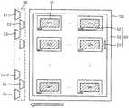
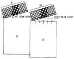
도 1을 참조하면, 본 발명의 일 실시예에 따른 기판(100)은 표시패널을 형성하기 위한 모기판으로 복수의 제1 영역(10)들과 상기 제1 영역을 제외한 나머지 부분인 제2 영역(50)을 포함한다. 상기 제1 영역(10)에는 매트릭스 타입으로 배열되는 다수의 패널(S11,..., Smn)들이 형성된다. 상기 제2 영역(50)은 상기 기판(100)의 고유번호가 형성되는 글라스 ID 영역(51) 및 상기 다수의 패널들의 고유번호가 형성되는 셀 ID 영역(52)을 포함한다. 또한, 상기 제2 영역(50)은 기판의 가장자리 부분인 에지 노광 영역(53)을 포함한다.Referring to FIG. 1, a
상기 기판(100)은 노광부(30)의 하부로 제1 방향(D11)을 따라 이송되어 노광된다. 상기 기판(100)은 하부에 배치된 스테이지(미도시)에 의해 상기 노광부(30)로 이송된다.The
상기 노광방식은 스텝 노광 또는 스캔 노광을 포함한다. 스텝 노광은 노광시 기판의 이동과 멈춤이 반복하는 동작이 포함된 것을 말하며, 스캔 노광은 노광시 기판의 연속적인 동작이 포함된 것을 말한다. 섬형 패턴(island pattern)은 주로 스텝 노광으로 형성할 수 있고, 스트립 패턴(strip pattern)은 주로 스캔 노광으로 형성할 수 있다.The exposure method includes a step exposure or a scan exposure. The step exposure refers to an operation of repeatedly moving and stopping the substrate during exposure, and the scan exposure refers to the continuous operation of the substrate during exposure. The island pattern can be formed mainly by a step exposure, and the strip pattern can be formed mainly by a scan exposure.
상기 노광부(30)는 복수의 노광헤드(E1, E2, E3,...EK-2, EK-1, EK)를 포함하고, 상기 복수의 노광헤드는 스캔 방향인 상기 제1 방향(D11)과 직교하는 제2방향(D12)을 따라 배열된다.(여기서, K는 자연수)The exposing
상기 복수의 노광헤드(E1, E2, E3,..., EK-2, EK-1, EK)는 예를 들어, 2열로 배열된다. 상기 제2 방향(D12)으로 배열된 제1 열의 노광헤드들과, 상기 제1 열과 근접하여 상기 제2 방향(D12)으로 배열된 제2 열의 노광헤드들은 교대로 배치될 수 있다. 상기 노광헤드들은 도시하지는 않았으나, 다양한 배열 형태로 상기 제2 방향(D12)을 따라 배열될 수 있다.The plurality of exposure heads E1, E2, E3, ..., EK-2, EK-1, EK are arranged in two rows, for example. The exposure heads of the first row arranged in the second direction D12 and the exposure heads of the second row arranged in the second direction D12 adjacent to the first row can be alternately arranged. The exposure heads may be arranged along the second direction D12 in various arrangements, though not shown.
고정된 상기 노광부(30)가 상기 제1 방향(D11)으로 이동하는 상기 기판(100)을 노광하므로 상기 기판(100)에는 상기 제1 방향(D11)과 반대방향으로 노광 패턴이 형성된다.An exposed pattern is formed on the
상기 노광헤드들은 디지털 마이크로 미러 디바이스(digital micro mirror device: DMD)를 포함한다. 상기 디지털 마이크로 미러 디바이스(DMD)는 온/오프 데이터에 노광빔을 조사할 수 있다. 상기 디지털 마이크로 미러 디바이스(DMD)의 해당 셀의 디지털 미러에서 소스 빔이 반사되어 상기 노광 빔이 생성되며, 상기 노광 빔은 상기 노광 헤드로부터 출사된다.The exposure heads include a digital micro mirror device (DMD). The digital micromirror device (DMD) may irradiate an on / off data with an exposure beam. In the digital mirror of the corresponding cell of the digital micromirror device (DMD), a source beam is reflected to generate the exposure beam, and the exposure beam is emitted from the exposure head.
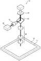
도 2는 도 1에 도시된 마스크리스 노광 장치의 일 실시예에 따른 노광 헤드를 나타낸 사시도이다.2 is a perspective view showing an exposure head according to an embodiment of the maskless exposure apparatus shown in FIG.
도 2를 참조하면, 상기 노광 헤드(31)는 상기 디지털 마이크로 미러 디바이스(DMD, 36)를 포함한다. 상기 디지털 마이크로 미러 디바이스(DMD, 36)는 노광원(40)으로부터 소스 빔을 전달받는다. 상기 소스 빔은 포토레지스트 노광용 자외선일 수 있다. 노광의 대상물인 피처리 기판(12)에는 감광막(11)이 형성되어 있다. 상기 감광막(11)은 기판에 패턴을 형성할 때, 상기 패턴의 마스크를 형성하기 위해 사용된다. 상기 감광막(11)은 유리 기판의 표면에 감광성 에폭시(epoxy) 수지 등의 감광성 수지를 도포하여 형성될 수 있다. 상기 디지털 마이크로 미러 디바이스(DMD, 36)는 상기 기판(100)에 전사될 화상 데이터에 기초하여 선택적으로 상기 소스 빔을 반사한다.Referring to FIG. 2, the
상기 노광 헤드(31)는 투영 광학계(38)을 포함한다. 상기 투영 광학계(38)는 다수의 렌즈들을 포함하며, 상기 디지털 마이크로 미러 디바이스(DMD, 36)로부터 선택적으로 반사된 반사광들을 상기 노광 빔으로 변환시킨다.The
도 3은 도 2에 도시된 노광 헤드를 이용한 노광 공정을 설명하기 위한 평면도이다.3 is a plan view for explaining an exposure process using the exposure head shown in FIG.
도 3을 참조하면, 상기 마스크리스 노광 장치는 상기 기판의 제1 방향(D1)으로 연장된 일 변을 기준으로 제1 각도(θ1)로 경사진 상태로 고정될 수 있다. 상기 제1 방향(D1)과 직교하는 방향을 제2 방향(D2)으로 정의할 때, 상기 마스크리스 노광장치가 경사진 방향은 상기 제1 방향(D1)과 상기 제2 방향(D2) 사이의 방향일 수 있다.Referring to FIG. 3, the maskless exposure apparatus may be fixed in a tilted state at a first angle? 1 with reference to one side extending in the first direction D1 of the substrate. When the direction orthogonal to the first direction D1 is defined as a second direction D2, the inclined direction of the maskless exposure apparatus is defined as a direction between the first direction D1 and the second direction D2 Direction.
구체적으로, 상기 마스크리스 노광 장치의 경사 방향은 양의 제1 방향(+D1)과 양의 제2 방향(+D2) 사이의 제3 방향(D3)일 수 있다. 상기 제1 각도(θ1)는 상기 제1 방향(D1)으로 연장된 기준선에 대해서 시계 방향으로 회전한 예각으로 정의될 수 있다. 예를 들어, 상기 제1 각도(θ1)는 약 0.1ㅀ 내지 약 0.5ㅀ일 수 있다.Specifically, the oblique direction of the maskless exposure apparatus may be a third direction D3 between a positive first direction (+ D1) and a positive second direction (+ D2). The first angle? 1 may be defined as an acute angle rotated clockwise with respect to a reference line extending in the first direction D1. For example, the first angle [theta] 1 may be between about 0.1 microns and about 0.5 microns.
상기 마스크리스 노광 장치가 상기 제3 방향(D3)으로 기울어진 상태에서, 스캔 방향(MD)을 따라 상기 기판(SUB)에 상기 스팟 빔들(20)을 제공할 수 있다. 상기 스캔 방향(MD)은 양의 제1 방향(+D1)과 실질적으로 동일할 수 있다. 상기 마스크리스 노광 장치의 상기 제1 각도(θ1)가 약 0ㅀ인 경우 상기 마스크리스 노광장치를 이용하여 상기 기판(SUB)을 상기 양의 제1 방향(+D1)을 따라 노광하면, 상기 기판(SUB)에서 서로 인접한 스팟 빔들(20) 사이의 영역에 대응하는 영역은 실질적으로 노광되지 않는다. 따라서, 소정의 면적을 갖는 영역을 전체적으로 노광하기 위해서는 상기 마스크리스 노광장치와 상기 기판(SUB)이 상기 제1 각도(θ1)로 기울어진 상태에서 노광 공정을 수행할 수 있다.The maskless exposure apparatus can provide the spot beams 20 to the substrate SUB along the scan direction MD in a state in which the maskless exposure apparatus is inclined in the third direction D3. The scan direction MD may be substantially the same as the positive first direction (+ D1). When the first angle (? 1) of the maskless exposure apparatus is about 0 占 When the substrate (SUB) is exposed along the positive first direction (+ D1) using the maskless exposure apparatus, The areas corresponding to the regions between the adjacent spot beams 20 in the sub-area SUB are not substantially exposed. Therefore, in order to expose the entire area having a predetermined area, the maskless exposure apparatus and the substrate SUB may be exposed with the first angle? 1 inclined.
상기 마이크로-미러들(222)이 모두 온 데이터를 받고 상기 기판(SUB)이 정지된 상태에서 상기 기판(SUB)에 상기 스팟 빔들(20)이 조사되는 경우, 상기 스팟 빔들(20)은 상기 제3 방향(D3)으로 소정 간격(x)으로 이격될 수 있다. 또한, 상기 스팟 빔들(20)은 상기 제3 방향(D3)과 직교하는 방향으로도 상기 소정 간격(x)으로 이격될 수 있다.When the spot beams 20 are irradiated to the substrate SUB while the substrate SUB is stopped and the micro-mirrors 222 receive all of the ON data, Can be spaced apart by a predetermined distance (x) in three directions (D3). The spot beams 20 may be spaced apart from each other by the predetermined distance x in a direction orthogonal to the third direction D3.
상기 마스크리스 노광 장치가 상기 기판(SUB)의 특정 영역, 예를 들어 패턴 형성 영역(L)만을 노광시키기 위해서는 상기 패턴 형성 영역(L)에만 상기 스팟 빔들(20)을 제공하여야 한다. 본 발명에서, 상기 패턴 형성 영역(L)은 상기 제2 방향(D2)으로 연장된 상기 기판(SUB)의 일변을 기준으로 시계 방향으로 제2 각도(θ2)로 기울어진 제4 방향(D4)을 따라 연장된다. 상기 패턴 형성 영역(L)은 사용자에 의해서 상기 제4 방향(D4)을 따라 연장된 라인 형태로 디자인될 수 있다. 상기 마스크리스 노광 장치에 의해 상기 패턴 형성 영역(L)이 전체적으로 노광된 때, 상기 패턴 형성 영역(L)에는 지름(2r)을 갖는 원형의 상기 스팟 빔들(20)이 상기 제4 방향(D4)을 따라 소정 간격(Δk)으로 중첩됨으로써 상기 패턴 형성 영역(L)이 전체적으로 노광된 것이라고 할 수 있다.The maskless exposure apparatus must provide the spot beams 20 only in the pattern formation region L in order to expose only a specific region of the substrate SUB, for example, the pattern formation region L. [ In the present invention, the pattern forming region L may include a fourth direction D4 that is inclined at a second angle? 2 in a clockwise direction with respect to one side of the substrate SUB extending in the second direction D2, Lt; / RTI > The pattern formation area L may be designed in a line shape extending along the fourth direction D4 by a user. The circular spot bumps 20 having a
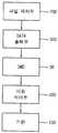
도 4는 도 1의 마스크리스 노광 장치의 일 실시예에 따른 시스템 제어부를 나타낸 블록도이다.4 is a block diagram showing a system control unit according to an embodiment of the maskless exposure apparatus of FIG.
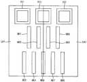
도 4를 참조하면, 상기 시스템 제어부는 파일제작부(200), 데이터 출력부(300) 및 이송 제어부(400)를 포함할 수 있다.Referring to FIG. 4, the system control unit may include a
상기 파일 제작부(200)는 그래픽 시스템 파일(GDS)을 제작한다. 상기 그래픽 데이터 시스템(GDS)파일은 여러 개의 층(layer)으로 구성된 캐드(CAD)파일이 변환된 것으로, 예를 들어, 게이트 패턴, 액티브 패턴, 소스 드레인 패턴 등의 각각의 레이어(layer)에 대한 데이터를 포함한다.The
상기 데이터 출력부(300)는 상기 그래픽 시스템 파일(GDS)로부터 상기 디지털 마이크로 미러 디바이스(DMD) 온/오프 데이터를 생성한다. 예를 들어, 상기 그래픽 시스템 파일(GDS)로부터 상기 디지털 마이크로 미러 디바이스(DMD) 온/오프 데이터를 생성한다.The
상기 데이터 출력부(300)는 상기 디지털 마이크로 미러 디바이스(DMD) 온/오프 데이터를 상기 디지털 마이크로 미러 디바이스(36)로 출력한다.The
상기 이송 제어부(400)는 상기 스테이지(미도시)를 이송시키는 이송 신호를 출력한다. 상기 이송 제어부(400)는 상기 데이터 출력부(300)로부터 인가되는 상기 디지털 마이크로 미러 디바이스 온/오프 데이터에 따라, 노광 빔들의 온 및 오프 타이밍을 제어하고, 상기 스테이지를 이송시킨다.The
본 실시예에 따른 마스크리스 노광 장치는 상기 기판(100)상의 패턴에 대한 상기 그래픽 데이터 시스템(GDS) 파일을 제작하는 단계, 상기 그래픽 데이터 시스템(GDS) 파일로부터 상기 디지털 마이크로 미러 디바이스(DMD) 온/오프 데이터를 생성하는 단계 및 상기 디지털 마이크로 미러 디바이스(DMD) 온/오프 데이터에 따라 상기 기판(100)을 노광하는 단계에 의해 표시 기판을 제작할 수 있다.The maskless exposure apparatus according to the present embodiment includes the steps of: producing the graphic data system (GDS) file for a pattern on the
상기 데이터 출력부(300)에서 상기 그래픽 데이터 시스템(GDS)파일로부터 상기 디지털 마이크로 미러 디바이스(DMD) 온/오프 데이터를 생성한다. 상기 온/오프 데이터를 생성하기 위한 온/오프 파일은 바이너리(binary file) 파일로서 1과 0으로 구성된다. 1은 상기 디지털 마이크로 미러 디바이스(DMD)가 온이 되게 하여 광을 기판에 전달할 수 있다. 0은 상기 디지털 마이크로 미러 디바이스(DMD)가 오프되게 하여 광이 기판에 전달되는 것을 차단한다.The
상기 디지털 마이크로 미러 디바이스(DMD)는 상기 온/오프 데이터에 따라 광을 선택적으로 반사하여, 상기 그래픽 데이터 시스템(GDS)파일에 저장된 상기 패턴의 데이터에 따라 상기 기판(100)을 노광한다. 따라서, 상기 패턴을 갖는 기판을 형성할 수 있다. The DMD selectively reflects light according to the on / off data and exposes the
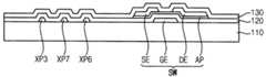
도 5는 본 발명의 일 실시예에 따른 노광 헤드의 디지털 마이크로 미러 디바이스에 이용되는 그래픽데이터 시스템(GDS) 파일의 X-얼라인키를 나타내는 평면도이다.5 is a plan view showing an X-aligned key of a graphic data system (GDS) file used in a digital micro mirror device of an exposure head according to an embodiment of the present invention.
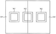
도 5를 참조하면, 본 발명의 일 실시예에 따른 X-얼라인키는 제1 노광 영역(EA1)에 배치되는 제1 서브 X-얼라인키(XK1), 제2 서브 X-얼라인키(XK2) 및 제3 서브 X-얼라인키(XK3), 상기 제1 노광 영역(EA1)과 인접하는 제2 노광 영역(EA2)에 배치되며 상기 제1 노광 영역(EA1)과 상기 제2 노광 영역(EA2)의 경계선을 기준으로 상기 제1 서브 X-얼라인키(XK1), 제2 서브 X-얼라인키(XK2) 및 제3 서브 X-얼라인키(XK3)와 대칭되도록 배치되는 제4 서브 X-얼라인키(XK4), 제5 서브 X-얼라인키(XK5) 및 제6 서브 X-얼라인키(XK6) 및 상기 제1 노광 영역(EA1)과 상기 제2 노광 영역(EA2)의 경계선 상에 배치되며, 상기 제1 노광 영역(EA1)과 상기 제2 노광 영역(EA2)의 경계선을 기준으로 대칭되는 형상을 갖는 제7 서브 X-얼라인키(XK7)를 포함한다.5, the X-alignment key according to an embodiment of the present invention includes a first sub-X-alignment key XK1, a second sub X-alignment key XK2, And a third sub-X-alignment key (XK3) arranged in the first exposure area (EA1) and a second exposure area (EA2) adjacent to the first exposure area (EA1) X-alignment key (XK1), the second sub-X-alignment key (XK2) and the third sub-X-alignment key (XK3) are symmetrical with respect to the boundary line of the first sub- (XK4), a fifth sub-X-alignment key (XK5), a sixth sub-X-alignment key (XK6), and a second exposure area (EA1) and a second exposure area (EA2) And a seventh sub X-alignment key (XK7) having a shape symmetrical with respect to a boundary line between the first exposure area (EA1) and the second exposure area (EA2).
상기 제1 내지 제7 서브 X-얼라인키들(XK1, XK2, XK3, XK4, XK5, XK6, XK7)은 동일한 폭을 가질 수 있다. 상기 제1 내지 제7 서브 X-얼라인키들(XK1, XK2, XK3, XK4, XK5, XK6, XK7)은 바(bar) 형상으로 형성될 수 있다.The first to seventh sub-X-alignment keys XK1, XK2, XK3, XK4, XK5, XK6 and XK7 may have the same width. The first to seventh sub-X-alignment marks XK1, XK2, XK3, XK4, XK5, XK6 and XK7 may be formed in a bar shape.
상기 제1 서브 X-얼라인키(XK1), 제2 서브 X-얼라인키(XK2), 제4 서브 X-얼라인키(XK4) 및 제5 서브 X-얼라인키(XK5)는 제1 행에 배치될 수 있다. 상기 제3 서브 X-얼라인키(XK3) 및 제6 서브 X-얼라인키(XK6)는 제2 행에 배치될 수있다.The first sub-X-alignment key XK1, the second sub-X-alignment key XK2, the fourth sub-X-alignment key XK4, and the fifth sub-X-alignment key XK5 are arranged in the first row . The third sub-X-alignment key (XK3) and the sixth sub-X-alignment key (XK6) may be arranged in the second row.
상기 제7 서브 X-얼라인키(XK7)는 상기 제1 노광 영역(EA1)과 상기 제2 노광 영역(EA2)의 경계선을 기준으로 대칭되는 형상을 가지므로, 상기 제7 서브 X-얼라인키(XK7)의 상기 제1 노광 영역(EA1)에 배치되는 부분과 상기 제7 서브 X-얼라인키(XK7)의 상기 제2 노광 영역(EA2)에 부분은 동일한 면적을 가질 수 있다.Since the seventh sub-X-alignment key (XK7) has a shape symmetrical with respect to the boundary line between the first exposure area (EA1) and the second exposure area (EA2), the seventh sub- XK7 in the first exposure area EA1 and the second sub-area XK7 in the second exposure area EA2 may have the same area.
상기 제1 노광 영역(EA1)과 상기 제2 노광 영역(EA2)을 노광하는 광학 헤드들이 틀어지지 않고 노광하는 경우 상기 제7 서브 X-얼라인키(XK7)에 의해 형성되는 패턴의 폭은 상기 제1 내지 제6 서브 X-얼라인키들(XK1, XK2, XK3, XK4, XK5, XK6)에 의해 형성되는 패턴들의 폭과 동일하게 형성될 수 있다. 그러나, 상기 제1 노광 영역(EA1)과 상기 제2 노광 영역(EA2)을 노광하는 광학 헤드들이 미스얼라인(mis-alignment)되어 노광하는 경우 상기 제7 서브 X-얼라인키(XK7)에 의해 형성되는 패턴의 폭은 상기 1 내지 제6 서브 X-얼라인키들(XK1, XK2, XK3, XK4, XK5, XK6)에 의해 형성되는 패턴들의 폭과 동일하게 형성되지 않게 된다.When the optical heads for exposing the first exposure area EA1 and the second exposure area EA2 are exposed without turning, the width of the pattern formed by the seventh sub-X-alignment key (XK7) XK1, XK2, XK3, XK4, XK5, XK6) of the first to sixth sub-X-alignment marks (XK1, XK2, XK3, XK4, XK5, XK6). However, when the optical heads for exposing the first exposure area EA1 and the second exposure area EA2 are misaligned and exposed, the seventh sub-X-alignment key XK7 The width of the pattern to be formed is not formed equal to the width of the patterns formed by the first to sixth sub-X-alignment marks XK1, XK2, XK3, XK4, XK5 and XK6.
따라서, 상기 7 서브 X-얼라인키(XK7)에 의해 형성되는 패턴의 폭과 상기 1 내지 제6 서브 X-얼라인키들(XK1, XK2, XK3, XK4, XK5, XK6)에 의해 형성되는 패턴들의 폭을 비교하여 상기 제1 노광 영역(EA1)과 상기 제2 노광 영역(EA2)을 노광하는 광학 헤드들의 X-성분 미스얼라인(mis-alignment) 여부를 확인할 수 있다.Therefore, the pattern formed by the 7th sub-X-alignment key (XK7) and the patterns formed by the 1st through 6th sub X-alignment keys (XK1, XK2, XK3, XK4, XK5, XK6) Component of the optical heads for exposing the first exposure area EA1 and the second exposure area EA2 by comparing the widths of the first and second exposure areas EA1 and EA2.
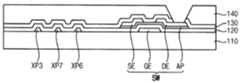
도 6은 본 발명의 일 실시예에 따른 노광 헤드의 디지털 마이크로 미러 디바이스에 이용되는 그래픽데이터 시스템(GDS) 파일의 X-얼라인키를 나타내는 평면도이다.6 is a plan view showing an X-aligned key of a graphic data system (GDS) file used in a digital micro mirror device of an exposure head according to an embodiment of the present invention.
도 6을 참조하면, 본 발명의 일 실시예에 따른 X-얼라인키는 제1 노광 영역(EA1)에 배치되는 제1 서브 X-얼라인키(XK1), 제2 서브 X-얼라인키(XK2), 제3 서브 X-얼라인키(XK3) 및 제4 서브 X-얼라인키(XK4), 상기 제1 노광 영역(EA1)과 인접하는 제2 노광 영역(EA2)에 배치되며 상기 제1 노광 영역(EA1)과 상기 제2 노광 영역(EA2)의 경계선을 기준으로 상기 제1 서브 X-얼라인키(XK1), 제2 서브 X-얼라인키(XK2), 제3 서브 X-얼라인키(XK3) 및 제4 서브 X-얼라인키(XK4)와 대칭되도록 배치되는 제5 서브 X-얼라인키(XK5), 제6 서브 X-얼라인키(XK6), 제7 서브 X-얼라인키(XK7) 및 제8 서브 X-얼라인키(XK8) 및 상기 제1 노광 영역(EA1)과 상기 제2 노광 영역(EA2)의 경계선 상에 배치되며, 상기 제1 노광 영역(EA1)과 상기 제2 노광 영역(EA2)의 경계선을 기준으로 대칭되는 형상을 갖는 제9 서브 X-얼라인키(XK9)를 포함한다.6, the X-alignment key according to an embodiment of the present invention includes a first sub-X-alignment key XK1, a second sub-X-alignment key XK2, , A third sub-X-alignment key (XK3) and a fourth sub-X-alignment key (XK4), and a second exposure area (EA2) adjacent to the first exposure area (EA1) The first sub-X-alignment key XK1, the second sub-X-alignment key XK2, the third sub-X-alignment key XK3, and the third sub- The fifth sub-X-alignment key (XK5), the sixth sub-X-alignment key (XK6), the seventh sub-X-alignment key (XK7), and the eighth A sub X-alignment key XK8 and a second exposure area EA2 disposed on a boundary line between the first exposure area EA1 and the second exposure area EA2, the first exposure area EA1 and the second exposure area EA2, (XK9) having a shape symmetrical with respect to the boundary line of the ninth sub-X- .
상기 제1 내지 제9 서브 X-얼라인키들(XK1, XK2, XK3, XK4, XK5, XK6, XK7, XK8, XK9)은 동일한 폭을 가질 수 있다. 상기 제1 내지 제9 서브 X-얼라인키들(XK1, XK2, XK3, XK4, XK5, XK6, XK7, XK8, XK9)은 바(bar) 형상으로 형성될 수 있다.The first to ninth sub-X-alignment keys XK1, XK2, XK3, XK4, XK5, XK6, XK7, XK8 and XK9 may have the same width. The first to ninth sub-X-alignment keys XK1, XK2, XK3, XK4, XK5, XK6, XK7, XK8 and XK9 may be formed in a bar shape.
상기 제1 서브 X-얼라인키(XK1), 제2 서브 X-얼라인키(XK2), 제5 서브 X-얼라인키(XK5) 및 제6 서브 X-얼라인키(XK6)는 제1 행에 배치될 수 있다. 상기 제3 서브 X-얼라인키(XK3), 제4 서브 X-얼라인키(XK4), 제7 서브 X-얼라인키(XK7) 및 제8 서브 X-얼라인키(XK8)는 제2 행에 배치될 수있다.The first sub-X-alignment key XK1, the second sub-X-alignment key XK2, the fifth sub-X-alignment key XK5, and the sixth sub-X-alignment key XK6 are arranged in the first row . The third sub-X-alignment key XK3, the fourth sub-X-alignment key XK4, the seventh sub-X-alignment key XK7 and the eighth sub- .
상기 제9 서브 X-얼라인키(XK9)는 상기 제1 노광 영역(EA1)과 상기 제2 노광 영역(EA2)의 경계선을 기준으로 대칭되는 형상을 가지므로, 상기 제9 서브 X-얼라인키(XK9)의 상기 제1 노광 영역(EA1)에 배치되는 부분과 상기 제9 서브 X-얼라인키(XK9)의 상기 제2 노광 영역(EA2)에 부분은 동일한 면적을 가질 수 있다.Since the ninth sub-X-alignment key (XK9) is symmetrical with respect to the boundary line between the first exposure area (EA1) and the second exposure area (EA2), the ninth sub- XK9 may have the same area as the portion of the ninth sub-X-alignment key (XK9) disposed in the first exposure area (EA1) and the second exposure area (EA2) of the ninth sub-
상기 제1 노광 영역(EA1)과 상기 제2 노광 영역(EA2)을 노광하는 광학 헤드들이 틀어지지 않고 노광하는 경우 상기 제9 서브 X-얼라인키(XK9)에 의해 형성되는 패턴의 폭은 상기 제1 내지 제8 서브 X-얼라인키들(XK1, XK2, XK3, XK4, XK5, XK6, XK7, XK8)에 의해 형성되는 패턴들의 폭과 동일하게 형성될 수 있다. 그러나, 상기 제1 노광 영역(EA1)과 상기 제2 노광 영역(EA2)을 노광하는 광학 헤드들이 미스얼라인(mis-alignment)되어 노광하는 경우 상기 제9 서브 X-얼라인키(XK9)에 의해 형성되는 패턴의 폭은 상기 1 내지 제8 서브 X-얼라인키들(XK1, XK2, XK3, XK4, XK5, XK6, XK7, XK8)에 의해 형성되는 패턴들의 폭과 동일하게 형성되지 않게 된다.When the optical heads for exposing the first exposure area EA1 and the second exposure area EA2 are exposed without turning, the width of the pattern formed by the ninth sub-X-alignment key (XK9) XK2, XK4, XK5, XK6, XK7, XK8) of the first to eighth sub-X-aligned pixels X1, X2, XK3, XK4, XK5, XK6, XK7, XK8. However, when the optical heads for exposing the first exposure area EA1 and the second exposure area EA2 are misaligned and exposed, the ninth sub-X-alignment key XK9 The width of the pattern to be formed is not formed equal to the width of the patterns formed by the first to eighth sub-X-alignment marks XK1, XK2, XK3, XK4, XK5, XK6, XK7 and XK8.
따라서, 상기 9 서브 X-얼라인키(XK9)에 의해 형성되는 패턴의 폭과 상기 1 내지 제8 서브 X-얼라인키들(XK1, XK2, XK3, XK4, XK5, XK6, XK7, XK8)에 의해 형성되는 패턴들의 폭을 비교하여 상기 제1 노광 영역(EA1)과 상기 제2 노광 영역(EA2)을 노광하는 광학 헤드들의 X-성분 미스얼라인(mis-alignment) 여부를 확인할 수 있다.Therefore, the width of the pattern formed by the 9 sub X-alignment marks (XK9) and the widths of the patterns formed by the first to eighth sub-X-alignment marks (XK1, XK2, XK3, XK4, XK5, XK6, XK7, XK8) It is possible to confirm whether the X-component mis-alignment of the optical heads exposing the first exposure area EA1 and the second exposure area EA2 by comparing the widths of the formed patterns.
도 7은 본 발명의 일 실시예에 따른 노광 헤드의 스캔들 사이의 X-성분 미스얼라인 상태를 나타내는 평면도이다. 도 8은 도 7의 A 부분을 확대한 평면도이다.7 is a plan view showing an X-component misalignment state between scans of an exposure head according to an embodiment of the present invention. 8 is an enlarged plan view of a portion A in Fig.
도 7 및 도 8을 참조하면, 광학 헤드의 제4 스캔(S4) 및 제5 스캔(S5)의 X-성분 미스얼라인 상태가 도시된다.Referring to Figs. 7 and 8, the X-component misaligned states of the fourth scan (S4) and the fifth scan (S5) of the optical head are shown.
한 개의 광학 헤드가 담당하는 노광 영역은 8 스캔일 수 있다. 예를 들어, 1 스캔은 66.5nm일 수 있다. 따라서, 하나의 광학 헤드가 담당하는 노광 영역은 532nm일 수 있다.The exposure area occupied by one optical head may be 8 scans. For example, one scan may be 66.5 nm. Therefore, the exposure area occupied by one optical head may be 532 nm.
노광 헤드의 스캔들 사이의 X-성분 미스얼라인은 스캔들 사이의 X-성분 영역이 좁아지는 경우와 미스얼라인은 스캔들 사이의 X-성분 영역이 넓어지는 경우를 포함한다.The X-component misalignment between the scans of the exposure head includes the case where the X-component region between the scans is narrowed and the misalignment includes the case where the X-component region between the scans is widened.
상기 제4 스캔(S4) 및 제5 스캔(S5)의 X-성분 미스얼라인 상태는 영역별로 다를 수 있다. 예를 들어, 상기 제4 스캔(S4) 및 제5 스캔(S5)의 제 4행에서는 제4 스캔(S4) 및 제5 스캔(S5) 사이의 영역이 좁아지며, 상기 제4 스캔(S4) 및 제5 스캔(S5)의 제 5행에서는 제 4스캔(S4) 및 제5 스캔(S5) 사이의 영역이 넓어진다.The X-component misalignment states of the fourth scan (S4) and the fifth scan (S5) may be different for each region. For example, in the fourth row of the fourth scan (S4) and the fifth scan (S5), the area between the fourth scan (S4) and the fifth scan (S5) becomes narrow, And the fifth scan (S5), the area between the fourth scan (S4) and the fifth scan (S5) is widened.
도 9는 본 발명의 일 실시예에 따른 노광 헤드의 디지털 마이크로 미러 디바이스에 이용되는 그래픽 데이터 시스템(GDS) 파일의 Y-얼라인키를 나타내는 평면도이다.9 is a plan view showing a Y-alignment key of a graphic data system (GDS) file used in a digital micromirror device of an exposure head according to an embodiment of the present invention.
도 9를 참조하면, 본 발명의 일 실시예에 따른 Y-얼라인키는 제1 노광 영역(EA1)에 배치되는 제1 서브 Y-얼라인키(YK1), 상기 제1 노광 영역(EA1)과 인접하는 제2 노광 영역(EA2)에 배치되며 상기 제1 노광 영역(EA1)과 상기 제2 노광 영역(EA2)의 경계선을 기준으로 상기 제1 서브 Y-얼라인키(YK1)와 대칭되도록 배치되는 제2 서브 Y-얼라인키(YK2) 및 상기 제1 노광 영역(EA1)과 상기 제2 노광 영역(EA2)의 경계선 상에 배치되며, 상기 제1 노광 영역(EA1)과 상기 제2 노광 영역(EA2)의 경계선을 기준으로 대칭되는 형상을 갖는 제3 서브 Y-얼라인키(YK3)를 포함한다.9, the Y-alignment key according to an embodiment of the present invention includes a first sub-Y-alignment key YK1 disposed in the first exposure area EA1, a second sub-Y-alignment key YK1 adjacent to the first exposure area EA1, Y-alignment key (YK1) arranged in the second exposure area (EA2) and symmetrical to the first sub-Y-alignment key (YK1) with reference to the boundary line between the first exposure area (EA1) and the
상기 제1 서브 Y-얼라인키(YK1), 상기 제2 서브 Y-얼라인키(YK2) 및 상기 제3 서브 Y-얼라인키(YK3)는 동일한 형상을 가질 수 있다. 상기 제1 서브 Y-얼라인키(YK1), 상기 제2 서브 Y-얼라인키(YK2) 및 상기 제3 서브 Y-얼라인키(YK3)는 사각틀 형상을 가질 수 있다.The first sub Y-alignment key YK1, the second sub Y-alignment key YK2, and the third sub Y-alignment key YK3 may have the same shape. The first sub Y-alignment key YK1, the second sub Y-alignment key YK2, and the third sub Y-alignment key YK3 may have a rectangular box shape.
상기 제3 서브 Y-얼라인키(YK3)는 상기 제1 노광 영역(EA1)과 상기 제2 노광 영역(EA2)의 경계선을 기준으로 대칭되는 형상을 가지므로, 상기 제3 서브 Y-얼라인키(YK3)의 상기 제1 노광 영역(EA1)에 배치되는 부분과 상기 제3 서브 Y-얼라인키(YK3)의 상기 제2 노광 영역(EA2)에 부분은 동일한 면적을 가질 수 있다.Since the third sub Y-alignment key YK3 has a shape symmetrical with respect to the boundary line between the first exposure area EA1 and the second exposure area EA2, the third sub-Y- YK3 may have the same area as the portion of the third sub Y-alignment key YK3 disposed in the first exposure area EA1 and the second exposure area EA2 of the third sub Y-alignment key YK3.
상기 제1 노광 영역(EA1)과 상기 제2 노광 영역(EA2)을 노광하는 광학 헤드들이 틀어지지 않고 노광하는 경우 상기 제3 서브 Y-얼라인키(YK3)에 의해 형성되는 패턴은 상기 제1 및 제2 서브 Y-얼라인키들(YK1, YK2)에 의해 형성되는 패턴들과 동일한 형상으로 형성될 수 있다. 그러나, 상기 제1 노광 영역(EA1)과 상기 제2 노광 영역(EA2)을 노광하는 광학 헤드들이 미스얼라인(mis-alignment)되어 노광하는 경우 상기 제3 서브 Y-얼라인키(YK3)에 의해 형성되는 패턴은 상기 제1 및 제2 서브 Y-얼라인키들(YK1, YK2)에 의해 형성되는 패턴들과 동일한 형상으로 형성되지 않게 된다.When the optical heads for exposing the first exposure area EA1 and the second exposure area EA2 are exposed without turning off, the pattern formed by the third sub-Y-alignment key YK3 is formed by the first and second sub- The second sub Y-alignment marks YK1 and YK2 may be formed in the same shape as the patterns formed by the second sub Y-alignment marks YK1 and YK2. However, when the optical heads for exposing the first exposure area EA1 and the second exposure area EA2 are misaligned and exposed, the third sub-Y-alignment key YK3 The pattern to be formed is not formed in the same shape as the patterns formed by the first and second sub Y-alignment keys YK1 and YK2.
따라서, 상기 제3 서브 Y-얼라인키(YK3)에 의해 형성되는 패턴의 형상과 상기 제1 및 제2 서브 Y-얼라인키들(YK1, YK2)에 의해 형성되는 패턴들의 형상을 비교하여 상기 제1 노광 영역(EA1)과 상기 제2 노광 영역(EA2)을 노광하는 광학 헤드들의 Y-성분 미스얼라인(mis-alignment) 여부를 확인할 수 있다.Therefore, by comparing the shape of the pattern formed by the third sub Y-alignment key (YK3) with the shapes of the patterns formed by the first and second sub Y-alignment keys (YK1, YK2) It is possible to confirm whether the Y-component misalignment of the optical heads exposing the first exposure area EA1 and the second exposure area EA2 is mis-alignment.
도 10은 본 발명의 일 실시예에 따른 노광 헤드의 스캔들 사이의 Y-성분 미스얼라인 상태를 나타내는 평면도이다. 도 11은 도 10의 B 부분을 확대한 평면도이다.10 is a plan view showing a Y-component misalignment state between scans of an exposure head according to an embodiment of the present invention. 11 is an enlarged plan view of a portion B in Fig.
도 10 및 도 11을 참조하면, 광학 헤드의 제1 스캔(S1) 내지 제8 스캔(S8)의 Y-성분 미스얼라인 상태가 도시된다.10 and 11, Y-component misaligned states of the first scan (S1) to the eighth scan (S8) of the optical head are shown.
한 개의 광학 헤드가 담당하는 노광 영역은 8 스캔일 수 있다. 예를 들어, 1 스캔은 66.5nm일 수 있다. 따라서, 하나의 광학 헤드가 담당하는 노광 영역은 532nm일 수 있다.The exposure area occupied by one optical head may be 8 scans. For example, one scan may be 66.5 nm. Therefore, the exposure area occupied by one optical head may be 532 nm.
노광 헤드의 스캔들 사이의 Y-성분 미스얼라인은 제2 스캔(S2)과 같이 노광 시작 위치가 낮은 경우와 제4 스캔(S4)과 같이 노광 시작 위치가 높은 경우를 포함한다.The Y-component misalignment between the scans of the exposure head includes a case where the exposure start position is low as in the second scan (S2) and a case where the exposure start position is high as in the fourth scan (S4).
노광 시작 위치는 각 스캔 마다 다를 수 있다. 예를 들어, 제7 스캔(S7)의 노광 시작 위치가 정상이라고 할 때, 제8 스캔(S8)의 노광 시작 위치는 상기 제7 스캔(S7)의 노광 시작 위치보다 낮게 형성된다. Y-성분 미스얼라인은 각 스캔 마다 발생할 수 있으며, 제1 스캔(S2)을 기준으로 제2 스캔(S2)의 Y-성분 미스 얼라인을 보정할 수 있다. 또한, 보정된 제2 스캔(S2)을 기준으로 제3 스캔(S3)의 Y-성분 미스 얼라인을 보정할 수 있다. 즉, 이전 스캔을 기준으로 다음 스캔의 Y-성분 미스 얼라인을 보정할 수 있다.The exposure start position may be different for each scan. For example, when the exposure start position of the seventh scan (S7) is normal, the exposure start position of the eighth scan (S8) is formed to be lower than the exposure start position of the seventh scan (S7). The Y-component misalignment may occur for each scan, and the Y-component misalignment of the second scan S2 may be corrected based on the first scan S2. Also, the Y-component misalignment of the third scan S3 can be corrected on the basis of the corrected second scan S2. That is, the Y-component misalignment of the next scan can be corrected based on the previous scan.
도 12는 본 발명의 일 실시예에 따른 노광 헤드의 디지털 마이크로 미러 디바이스에 이용되는 그래픽 데이터 시스템(GDS) 파일의 X-얼라인키 및 Y-얼라인키를 나타내는 평면도이다.12 is a plan view showing an X-alignment key and a Y-alignment key of a graphic data system (GDS) file used in a digital micromirror device of an exposure head according to an embodiment of the present invention.
도 12를 참조하면, 본 발명의 일 실시예에 따른 노광 헤드의 디지털 마이크로 미러 디바이스에 이용되는 그래픽데이터 시스템(GDS) 파일은 X-얼라인키 및 Y-얼라인키를 포함한다. 상기 Y-얼라인키는 상기 X-얼라인키의 상부에 배치될 수 있다.Referring to FIG. 12, a graphic data system (GDS) file used in a digital micromirror device of an exposure head according to an embodiment of the present invention includes an X-alignment key and a Y-alignment key. The Y-alignment key may be placed on top of the X-alignment key.
상기 X-얼라인키는 제1 노광 영역(EA1)에 배치되는 제1 서브 X-얼라인키(XK1), 제2 서브 X-얼라인키(XK2) 및 제3 서브 X-얼라인키(XK3), 상기 제1 노광 영역(EA1)과 인접하는 제2 노광 영역(EA2)에 배치되며 상기 제1 노광 영역(EA1)과 상기 제2 노광 영역(EA2)의 경계선을 기준으로 상기 제1 서브 X-얼라인키(XK1), 제2 서브 X-얼라인키(XK2) 및 제3 서브 X-얼라인키(XK3)와 대칭되도록 배치되는 제4 서브 X-얼라인키(XK4), 제5 서브 X-얼라인키(XK5) 및 제6 서브 X-얼라인키(XK6) 및 상기 제1 노광 영역(EA1)과 상기 제2 노광 영역(EA2)의 경계선 상에 배치되며, 상기 제1 노광 영역(EA1)과 상기 제2 노광 영역(EA2)의 경계선을 기준으로 대칭되는 형상을 갖는 제7 서브 X-얼라인키(XK7)를 포함한다.The X-alignment key includes a first sub-X-alignment key XK1, a second sub-X-alignment key XK2 and a third sub-X-alignment key XK3 arranged in the first exposure area EA1, The exposure apparatus according to
상기 제1 내지 제7 서브 X-얼라인키들(XK1, XK2, XK3, XK4, XK5, XK6, XK7)은 동일한 폭을 가질 수 있다. 상기 제1 내지 제7 서브 X-얼라인키들(XK1, XK2, XK3, XK4, XK5, XK6, XK7)은 바(bar) 형상으로 형성될 수 있다.The first to seventh sub-X-alignment keys XK1, XK2, XK3, XK4, XK5, XK6 and XK7 may have the same width. The first to seventh sub-X-alignment marks XK1, XK2, XK3, XK4, XK5, XK6 and XK7 may be formed in a bar shape.
상기 제1 서브 X-얼라인키(XK1), 제2 서브 X-얼라인키(XK2), 제4 서브 X-얼라인키(XK4) 및 제5 서브 X-얼라인키(XK5)는 제1 행에 배치될 수 있다. 상기 제3 서브 X-얼라인키(XK3) 및 제6 서브 X-얼라인키(XK6)는 제2 행에 배치될 수 있다.The first sub-X-alignment key XK1, the second sub-X-alignment key XK2, the fourth sub-X-alignment key XK4, and the fifth sub-X-alignment key XK5 are arranged in the first row . The third sub-X-alignment key (XK3) and the sixth sub-X-alignment key (XK6) may be arranged in the second row.
상기 제7 서브 X-얼라인키(XK7)는 상기 제1 노광 영역(EA1)과 상기 제2 노광 영역(EA2)의 경계선을 기준으로 대칭되는 형상을 가지므로, 상기 제7 서브 X-얼라인키(XK7)의 상기 제1 노광 영역(EA1)에 배치되는 부분과 상기 제7 서브 X-얼라인키(XK7)의 상기 제2 노광 영역(EA2)에 부분은 동일한 면적을 가질 수 있다.Since the seventh sub-X-alignment key (XK7) has a shape symmetrical with respect to the boundary line between the first exposure area (EA1) and the second exposure area (EA2), the seventh sub- XK7 in the first exposure area EA1 and the second sub-area XK7 in the second exposure area EA2 may have the same area.
상기 제1 노광 영역(EA1)과 상기 제2 노광 영역(EA2)을 노광하는 광학 헤드들이 틀어지지 않고 노광하는 경우 상기 제7 서브 X-얼라인키(XK7)에 의해 형성되는 패턴의 폭은 상기 제1 내지 제6 서브 X-얼라인키들(XK1, XK2, XK3, XK4, XK5, XK6)에 의해 형성되는 패턴들의 폭과 동일하게 형성될 수 있다. 그러나, 상기 제1 노광 영역(EA1)과 상기 제2 노광 영역(EA2)을 노광하는 광학 헤드들이 미스얼라인(mis-alignment)되어 노광하는 경우 상기 제7 서브 X-얼라인키(XK7)에 의해 형성되는 패턴의 폭은 상기 1 내지 제6 서브 X-얼라인키들(XK1, XK2, XK3, XK4, XK5, XK6)에 의해 형성되는 패턴들의 폭과 동일하게 형성되지 않게 된다.When the optical heads for exposing the first exposure area EA1 and the second exposure area EA2 are exposed without turning, the width of the pattern formed by the seventh sub-X-alignment key (XK7) XK1, XK2, XK3, XK4, XK5, XK6) of the first to sixth sub-X-alignment marks (XK1, XK2, XK3, XK4, XK5, XK6). However, when the optical heads for exposing the first exposure area EA1 and the second exposure area EA2 are misaligned and exposed, the seventh sub-X-alignment key XK7 The width of the pattern to be formed is not formed equal to the width of the patterns formed by the first to sixth sub-X-alignment marks XK1, XK2, XK3, XK4, XK5 and XK6.
따라서, 상기 7 서브 X-얼라인키(XK7)에 의해 형성되는 패턴의 폭과 상기 1 내지 제6 서브 X-얼라인키들(XK1, XK2, XK3, XK4, XK5, XK6)에 의해 형성되는 패턴들의 폭을 비교하여 상기 제1 노광 영역(EA1)과 상기 제2 노광 영역(EA2)을 노광하는 광학 헤드들의 X-성분 미스얼라인(mis-alignment) 여부를 확인할 수 있다.Therefore, the pattern formed by the 7th sub-X-alignment key (XK7) and the patterns formed by the 1st through 6th sub X-alignment keys (XK1, XK2, XK3, XK4, XK5, XK6) Component of the optical heads for exposing the first exposure area EA1 and the second exposure area EA2 by comparing the widths of the first and second exposure areas EA1 and EA2.
상기 Y-얼라인키는 제1 노광 영역(EA1)에 배치되는 제1 서브 Y-얼라인키(YK1), 상기 제1 노광 영역(EA1)과 인접하는 제2 노광 영역(EA2)에 배치되며 상기 제1 노광 영역(EA1)과 상기 제2 노광 영역(EA2)의 경계선을 기준으로 상기 제1 서브 Y-얼라인키(YK1)와 대칭되도록 배치되는 제2 서브 Y-얼라인키(YK2) 및 상기 제1 노광 영역(EA1)과 상기 제2 노광 영역(EA2)의 경계선 상에 배치되며, 상기 제1 노광 영역(EA1)과 상기 제2 노광 영역(EA2)의 경계선을 기준으로 대칭되는 형상을 갖는 제3 서브 Y-얼라인키(YK3)를 포함한다.The Y-alignment key includes a first sub Y-alignment key (YK1) arranged in a first exposure area (EA1), a second sub-Y alignment key (YK1) arranged in a second exposure area (EA2) adjacent to the first exposure area A second sub Y-alignment key (YK2) arranged to be symmetrical with the first sub Y-alignment key (YK1) with reference to a boundary line between the first exposure area (EA1) and the second exposure area (EA2) And a third exposure area EA2 disposed on the boundary line between the exposure area EA1 and the second exposure area EA2 and symmetrical with respect to the boundary line between the first exposure area EA1 and the second exposure area EA2, And a sub Y-alignment key (YK3).
상기 제1 서브 Y-얼라인키(YK1), 상기 제2 서브 Y-얼라인키(YK2) 및 상기 제3 서브 Y-얼라인키(YK3)는 동일한 형상을 가질 수 있다. 상기 제1 서브 Y-얼라인키(YK1), 상기 제2 서브 Y-얼라인키(YK2) 및 상기 제3 서브 Y-얼라인키(YK3)는 사각틀 형상을 가질 수 있다.The first sub Y-alignment key YK1, the second sub Y-alignment key YK2, and the third sub Y-alignment key YK3 may have the same shape. The first sub Y-alignment key YK1, the second sub Y-alignment key YK2, and the third sub Y-alignment key YK3 may have a rectangular box shape.
상기 제3 서브 Y-얼라인키(YK3)는 상기 제1 노광 영역(EA1)과 상기 제2 노광 영역(EA2)의 경계선을 기준으로 대칭되는 형상을 가지므로, 상기 제3 서브 Y-얼라인키(YK3)의 상기 제1 노광 영역(EA1)에 배치되는 부분과 상기 제3 서브 Y-얼라인키(YK3)의 상기 제2 노광 영역(EA2)에 부분은 동일한 면적을 가질 수 있다.Since the third sub Y-alignment key YK3 has a shape symmetrical with respect to the boundary line between the first exposure area EA1 and the second exposure area EA2, the third sub-Y- YK3 may have the same area as the portion of the third sub Y-alignment key YK3 disposed in the first exposure area EA1 and the second exposure area EA2 of the third sub Y-alignment key YK3.
상기 제1 노광 영역(EA1)과 상기 제2 노광 영역(EA2)을 노광하는 광학 헤드들이 틀어지지 않고 노광하는 경우 상기 제3 서브 Y-얼라인키(YK3)에 의해 형성되는 패턴은 상기 제1 및 제2 서브 Y-얼라인키들(YK1, YK2)에 의해 형성되는 패턴들과 동일한 형상으로 형성될 수 있다. 그러나, 상기 제1 노광 영역(EA1)과 상기 제2 노광 영역(EA2)을 노광하는 광학 헤드들이 미스얼라인(mis-alignment)되어 노광하는 경우 상기 제3 서브 Y-얼라인키(YK3)에 의해 형성되는 패턴은 상기 제1 및 제2 서브 Y-얼라인키들(YK1, YK2)에 의해 형성되는 패턴들과 동일한 형상으로 형성되지 않게 된다.When the optical heads for exposing the first exposure area EA1 and the second exposure area EA2 are exposed without turning off, the pattern formed by the third sub-Y-alignment key YK3 is formed by the first and second sub- The second sub Y-alignment marks YK1 and YK2 may be formed in the same shape as the patterns formed by the second sub Y-alignment marks YK1 and YK2. However, when the optical heads for exposing the first exposure area EA1 and the second exposure area EA2 are misaligned and exposed, the third sub-Y-alignment key YK3 The pattern to be formed is not formed in the same shape as the patterns formed by the first and second sub Y-alignment keys YK1 and YK2.
따라서, 상기 제3 서브 Y-얼라인키(YK3)에 의해 형성되는 패턴의 형상과 상기 제1 및 제2 서브 Y-얼라인키들(YK1, YK2)에 의해 형성되는 패턴들의 형상을 비교하여 상기 제1 노광 영역(EA1)과 상기 제2 노광 영역(EA2)을 노광하는 광학 헤드들의 Y-성분 미스얼라인(mis-alignment) 여부를 확인할 수 있다.Therefore, by comparing the shape of the pattern formed by the third sub Y-alignment key (YK3) with the shapes of the patterns formed by the first and second sub Y-alignment keys (YK1, YK2) It is possible to confirm whether the Y-component misalignment of the optical heads exposing the first exposure area EA1 and the second exposure area EA2 is mis-alignment.
도 13은 본 발명의 일 실시예에 따른 노광 헤드의 디지털 마이크로 미러 디바이스에 이용되는 그래픽 데이터 시스템(GDS) 파일의 X-얼라인키 및 Y-얼라인키를 나타내는 평면도이다.13 is a plan view showing an X-alignment key and a Y-alignment key of a graphics data system (GDS) file used in a digital micromirror device of an exposure head according to an embodiment of the present invention.
도 13을 참조하면, 본 발명의 일 실시예에 따른 노광 헤드의 디지털 마이크로 미러 디바이스에 이용되는 그래픽 데이터 시스템(GDS) 파일은 X-얼라인키 및 Y-얼라인키를 포함한다. 상기 Y-얼라인키는 상기 X-얼라인키의 상부에 배치될 수 있다.Referring to FIG. 13, a graphic data system (GDS) file used in a digital micro mirror device of an exposure head according to an embodiment of the present invention includes an X-alignment key and a Y-alignment key. The Y-alignment key may be placed on top of the X-alignment key.
상기 X-얼라인키는 제1 노광 영역(EA1)에 배치되는 제1 서브 X-얼라인키(XK1), 제2 서브 X-얼라인키(XK2), 제3 서브 X-얼라인키(XK3) 및 제4 서브 X-얼라인키(XK4), 상기 제1 노광 영역(EA1)과 인접하는 제2 노광 영역(EA2)에 배치되며 상기 제1 노광 영역(EA1)과 상기 제2 노광 영역(EA2)의 경계선을 기준으로 상기 제1 서브 X-얼라인키(XK1), 제2 서브 X-얼라인키(XK2), 제3 서브 X-얼라인키(XK3) 및 제4 서브 X-얼라인키(XK4)와 대칭되도록 배치되는 제5 서브 X-얼라인키(XK5), 제6 서브 X-얼라인키(XK6), 제7 서브 X-얼라인키(XK7) 및 제8 서브 X-얼라인키(XK8) 및 상기 제1 노광 영역(EA1)과 상기 제2 노광 영역(EA2)의 경계선 상에 배치되며, 상기 제1 노광 영역(EA1)과 상기 제2 노광 영역(EA2)의 경계선을 기준으로 대칭되는 형상을 갖는 제9 서브 X-얼라인키(XK9)를 포함한다.The X-alignment key includes a first sub-X-alignment key (XK1), a second sub-X-alignment key (XK2), a third sub-X-alignment key (XK3) A first exposure area EA2 and a fourth exposure area EA2 disposed in the second exposure area EA2 adjacent to the first exposure area EA1 and the sub X- (XK1), the second sub-X-alignment key (XK2), the third sub-X-alignment key (XK3), and the fourth sub-X-alignment key (XK4) (XK5), the sixth sub-X-alignment key (XK6), the seventh sub-X-alignment key (XK7), the eighth sub-X-alignment key (XK8) and the first sub- The first exposure area EA1 and the second exposure area EA2 are symmetrical with respect to the boundary line between the first exposure area EA1 and the second exposure area EA2, X-allin key (XK9).
상기 제1 내지 제9 서브 X-얼라인키들(XK1, XK2, XK3, XK4, XK5, XK6, XK7, XK8, XK9)은 동일한 폭을 가질 수 있다. 상기 제1 내지 제9 서브 X-얼라인키들(XK1, XK2, XK3, XK4, XK5, XK6, XK7, XK8, XK9)은 바(bar) 형상으로 형성될 수 있다.The first to ninth sub-X-alignment keys XK1, XK2, XK3, XK4, XK5, XK6, XK7, XK8 and XK9 may have the same width. The first to ninth sub-X-alignment keys XK1, XK2, XK3, XK4, XK5, XK6, XK7, XK8 and XK9 may be formed in a bar shape.
상기 제1 서브 X-얼라인키(XK1), 제2 서브 X-얼라인키(XK2), 제5 서브 X-얼라인키(XK5) 및 제6 서브 X-얼라인키(XK6)는 제1 행에 배치될 수 있다. 상기 제3 서브 X-얼라인키(XK3), 제4 서브 X-얼라인키(XK4), 제7 서브 X-얼라인키(XK7) 및 제8 서브 X-얼라인키(XK8)는 제2 행에 배치될 수있다.The first sub-X-alignment key XK1, the second sub-X-alignment key XK2, the fifth sub-X-alignment key XK5, and the sixth sub-X-alignment key XK6 are arranged in the first row . The third sub-X-alignment key XK3, the fourth sub-X-alignment key XK4, the seventh sub-X-alignment key XK7 and the eighth sub- .
상기 제9 서브 X-얼라인키(XK9)는 상기 제1 노광 영역(EA1)과 상기 제2 노광 영역(EA2)의 경계선을 기준으로 대칭되는 형상을 가지므로, 상기 제9 서브 X-얼라인키(XK9)의 상기 제1 노광 영역(EA1)에 배치되는 부분과 상기 제9 서브 X-얼라인키(XK9)의 상기 제2 노광 영역(EA2)에 부분은 동일한 면적을 가질 수 있다.Since the ninth sub-X-alignment key (XK9) is symmetrical with respect to the boundary line between the first exposure area (EA1) and the second exposure area (EA2), the ninth sub- XK9 may have the same area as the portion of the ninth sub-X-alignment key (XK9) disposed in the first exposure area (EA1) and the second exposure area (EA2) of the ninth sub-
상기 제1 노광 영역(EA1)과 상기 제2 노광 영역(EA2)을 노광하는 광학 헤드들이 틀어지지 않고 노광하는 경우 상기 제9 서브 X-얼라인키(XK9)에 의해 형성되는 패턴의 폭은 상기 제1 내지 제8 서브 X-얼라인키들(XK1, XK2, XK3, XK4, XK5, XK6, XK7, XK8)에 의해 형성되는 패턴들의 폭과 동일하게 형성될 수 있다. 그러나, 상기 제1 노광 영역(EA1)과 상기 제2 노광 영역(EA2)을 노광하는 광학 헤드들이 미스얼라인(mis-alignment)되어 노광하는 경우 상기 제9 서브 X-얼라인키(XK9)에 의해 형성되는 패턴의 폭은 상기 1 내지 제8 서브 X-얼라인키들(XK1, XK2, XK3, XK4, XK5, XK6, XK7, XK8)에 의해 형성되는 패턴들의 폭과 동일하게 형성되지 않게 된다.When the optical heads for exposing the first exposure area EA1 and the second exposure area EA2 are exposed without turning, the width of the pattern formed by the ninth sub-X-alignment key (XK9) XK2, XK4, XK5, XK6, XK7, XK8) of the first to eighth sub-X-aligned pixels X1, X2, XK3, XK4, XK5, XK6, XK7, XK8. However, when the optical heads for exposing the first exposure area EA1 and the second exposure area EA2 are misaligned and exposed, the ninth sub-X-alignment key XK9 The width of the pattern to be formed is not formed equal to the width of the patterns formed by the first to eighth sub-X-alignment marks XK1, XK2, XK3, XK4, XK5, XK6, XK7 and XK8.
따라서, 상기 9 서브 X-얼라인키(XK9)에 의해 형성되는 패턴의 폭과 상기 1 내지 제8 서브 X-얼라인키들(XK1, XK2, XK3, XK4, XK5, XK6, XK7, XK8)에 의해 형성되는 패턴들의 폭을 비교하여 상기 제1 노광 영역(EA1)과 상기 제2 노광 영역(EA2)을 노광하는 광학 헤드들의 X-성분 미스얼라인(mis-alignment) 여부를 확인할 수 있다.Therefore, the width of the pattern formed by the 9 sub X-alignment marks (XK9) and the widths of the patterns formed by the first to eighth sub-X-alignment marks (XK1, XK2, XK3, XK4, XK5, XK6, XK7, XK8) It is possible to confirm whether the X-component mis-alignment of the optical heads exposing the first exposure area EA1 and the second exposure area EA2 by comparing the widths of the formed patterns.
상기 Y-얼라인키는 제1 노광 영역(EA1)에 배치되는 제1 서브 Y-얼라인키(YK1), 상기 제1 노광 영역(EA1)과 인접하는 제2 노광 영역(EA2)에 배치되며 상기 제1 노광 영역(EA1)과 상기 제2 노광 영역(EA2)의 경계선을 기준으로 상기 제1 서브 Y-얼라인키(YK1)와 대칭되도록 배치되는 제2 서브 Y-얼라인키(YK2) 및 상기 제1 노광 영역(EA1)과 상기 제2 노광 영역(EA2)의 경계선 상에 배치되며, 상기 제1 노광 영역(EA1)과 상기 제2 노광 영역(EA2)의 경계선을 기준으로 대칭되는 형상을 갖는 제3 서브 Y-얼라인키(YK3)를 포함한다.The Y-alignment key includes a first sub Y-alignment key (YK1) arranged in a first exposure area (EA1), a second sub-Y alignment key (YK1) arranged in a second exposure area (EA2) adjacent to the first exposure area A second sub Y-alignment key (YK2) arranged to be symmetrical with the first sub Y-alignment key (YK1) with reference to a boundary line between the first exposure area (EA1) and the second exposure area (EA2) And a third exposure area EA2 disposed on the boundary line between the exposure area EA1 and the second exposure area EA2 and symmetrical with respect to the boundary line between the first exposure area EA1 and the second exposure area EA2, And a sub Y-alignment key (YK3).
상기 제1 서브 Y-얼라인키(YK1), 상기 제2 서브 Y-얼라인키(YK2) 및 상기 제3 서브 Y-얼라인키(YK3)는 동일한 형상을 가질 수 있다. 상기 제1 서브 Y-얼라인키(YK1), 상기 제2 서브 Y-얼라인키(YK2) 및 상기 제3 서브 Y-얼라인키(YK3)는 사각틀 형상을 가질 수 있다.The first sub Y-alignment key YK1, the second sub Y-alignment key YK2, and the third sub Y-alignment key YK3 may have the same shape. The first sub Y-alignment key YK1, the second sub Y-alignment key YK2, and the third sub Y-alignment key YK3 may have a rectangular box shape.
상기 제3 서브 Y-얼라인키(YK3)는 상기 제1 노광 영역(EA1)과 상기 제2 노광 영역(EA2)의 경계선을 기준으로 대칭되는 형상을 가지므로, 상기 제3 서브 Y-얼라인키(YK3)의 상기 제1 노광 영역(EA1)에 배치되는 부분과 상기 제3 서브 Y-얼라인키(YK3)의 상기 제2 노광 영역(EA2)에 부분은 동일한 면적을 가질 수 있다.Since the third sub Y-alignment key YK3 has a shape symmetrical with respect to the boundary line between the first exposure area EA1 and the second exposure area EA2, the third sub-Y- YK3 may have the same area as the portion of the third sub Y-alignment key YK3 disposed in the first exposure area EA1 and the second exposure area EA2 of the third sub Y-alignment key YK3.
상기 제1 노광 영역(EA1)과 상기 제2 노광 영역(EA2)을 노광하는 광학 헤드들이 틀어지지 않고 노광하는 경우 상기 제3 서브 Y-얼라인키(YK3)에 의해 형성되는 패턴은 상기 제1 및 제2 서브 Y-얼라인키들(YK1, YK2)에 의해 형성되는 패턴들과 동일한 형상으로 형성될 수 있다. 그러나, 상기 제1 노광 영역(EA1)과 상기 제2 노광 영역(EA2)을 노광하는 광학 헤드들이 미스얼라인(mis-alignment)되어 노광하는 경우 상기 제3 서브 Y-얼라인키(YK3)에 의해 형성되는 패턴은 상기 제1 및 제2 서브 Y-얼라인키들(YK1, YK2)에 의해 형성되는 패턴들과 동일한 형상으로 형성되지 않게 된다.When the optical heads for exposing the first exposure area EA1 and the second exposure area EA2 are exposed without turning off, the pattern formed by the third sub-Y-alignment key YK3 is formed by the first and second sub- The second sub Y-alignment marks YK1 and YK2 may be formed in the same shape as the patterns formed by the second sub Y-alignment marks YK1 and YK2. However, when the optical heads for exposing the first exposure area EA1 and the second exposure area EA2 are misaligned and exposed, the third sub-Y-alignment key YK3 The pattern to be formed is not formed in the same shape as the patterns formed by the first and second sub Y-alignment keys YK1 and YK2.
따라서, 상기 제3 서브 Y-얼라인키(YK3)에 의해 형성되는 패턴의 형상과 상기 제1 및 제2 서브 Y-얼라인키들(YK1, YK2)에 의해 형성되는 패턴들의 형상을 비교하여 상기 제1 노광 영역(EA1)과 상기 제2 노광 영역(EA2)을 노광하는 광학 헤드들의 Y-성분 미스얼라인(mis-alignment) 여부를 확인할 수 있다.Therefore, by comparing the shape of the pattern formed by the third sub Y-alignment key (YK3) with the shapes of the patterns formed by the first and second sub Y-alignment keys (YK1, YK2) It is possible to confirm whether the Y-component misalignment of the optical heads exposing the first exposure area EA1 and the second exposure area EA2 is mis-alignment.
도 14는 본 발명의 일 실시예에 따른 마스크리스 노광 방법의 X-성분 미스얼라인 보정 방법을 나타낸 블록도이다.14 is a block diagram showing an X-component misalignment correction method of a maskless exposure method according to an embodiment of the present invention.
도 14를 참조하면, 본 발명의 일 실시예에 따른 마스크리스 노광 방법의 X-성분 미스얼라인 보정 방법은 기판 상에 상기 제1 내지 제7 서브 X-얼라인키들에 대응되게 형성되는 제1 내지 제7 X-얼라인키 패턴들의 폭을 측정하는 단계(S110), 제1 노광 영역에 형성되는 X-얼라인키 패턴들의 폭의 평균값과 제2 노광 영역에 형성되는 X-얼라인키 패턴들의 폭의 평균값을 계산하는 단계(S120), 경계부의 X-얼라인키 패턴의 타겟 폭을 계산하는 단계(S130), 상기 경계부의 X-얼라인키 패턴의 타겟 폭과 실제 경계부의 X-얼라인키 패턴의 폭을 비교하는 단계(S140) 및 상기 X-얼라인키 패턴의 타겟 폭과 상기 제7 X-얼라인키 패턴의 폭의 차이를 이용하여 제1 방향으로 연장되는 X-성분의 미스얼라인을 보정하는 제1 보정 데이터를 생성하는 단계(S150)를 포함한다.Referring to FIG. 14, an X-component misalignment correction method of a maskless exposure method according to an embodiment of the present invention includes a first X- (S110) of measuring the width of the X-aligned key patterns formed in the first exposure area, measuring the width of the X-aligned key patterns formed in the second exposure area (S130) calculating a target width of the X-aligned key pattern at the boundary, calculating a target width of the X-aligned key pattern at the boundary and a width of the X- (S140) for correcting misalignment of an X-component extending in a first direction using a difference between a width of the X-aligned key pattern and a width of the seventh X-aligned key pattern, And generating the correction data (S150).
기판 상에 상기 제1 내지 제7 서브 X-얼라인키들에 대응되게 형성되는 제1 내지 제7 X-얼라인키 패턴들의 폭을 측정한다. 이후, 측정된 상기 X-얼라인키 패턴들의 폭을 이용하여 제1 노광 영역에 형성되는 X-얼라인키 패턴들의 폭의 평균값과 제2 노광 영역에 형성되는 X-얼라인키 패턴들의 폭의 평균값을 계산한다.The widths of the first to seventh X-aligned key patterns formed corresponding to the first to seventh sub-X-aligned keys on the substrate are measured. Then, the average of the widths of the X-aligned key patterns formed in the first exposure area and the width of the X-aligned key patterns formed in the second exposure area are calculated using the widths of the measured X- do.
상기 제1 노광 영역에 형성되는 X-얼라인키 패턴들의 폭의 평균값과 제2 노광 영역에 형성되는 X-얼라인키 패턴들의 폭의 평균값을 계산하는 단계(S120)에서는 X-얼라인키 패턴이 7개 형성되는 경우 상기 제1 내지 제3 X-얼라인키 패턴들의 폭의 평균값 및 제4 내지 제6 X-얼라인키 패턴들의 폭의 평균값을 계산한다. 또한, X-얼라인키 패턴이9개 형성되는 경우, 상기 제1 내지 제4 X-얼라인키 패턴들의 폭의 평균값 및 제5 내지 제8 X-얼라인키 패턴들의 폭의 평균값을 계산한다.In step S120 of calculating the average value of the widths of the X-aligned key patterns formed in the first exposure area and the widths of the X-aligned key patterns formed in the second exposure area, the X- The average value of the widths of the first to third X-aligned key patterns and the average value of the widths of the fourth to sixth X-aligned key patterns are calculated. In addition, when nine X-aligned key patterns are formed, an average value of the widths of the first to fourth X-aligned key patterns and an average value of the widths of the fifth to eighth X-aligned key patterns are calculated.
경계부의 X-얼라인키 패턴의 타겟 폭을 계산하는 단계(S130)에서는 X-얼라인키 패턴이 7개 형성되는 경우, 상기 제1 내지 제3 X-얼라인키 패턴들의 폭의 평균값을 2로 나눈 값과 제4 내지 제6 X-얼라인키 패턴들의 폭의 평균값을 2로 나눈 값을 더하여 경계부의 X-얼라인키 패턴의 타겟 폭을 계산한다. 또한, X-얼라인키 패턴이9개 형성되는 경우, 상기 제1 내지 제4 X-얼라인키 패턴들의 폭의 평균값을 2로 나눈값과 제5 내지 제8 X-얼라인키 패턴들의 폭의 평균값을 2로 나눈 값을 더하여 경계부의 X-얼라인키 패턴의 타겟 폭을 계산한다.In step S130 of calculating the target width of the X-aligned key pattern at the boundary, when seven X-aligned key patterns are formed, the average value of the widths of the first to third X- And a value obtained by dividing the average value of the widths of the 4th to 6th X-aligned key patterns by 2 is added to calculate the target width of the X-aligned key pattern at the boundary. When nine X-aligned key patterns are formed, the average value of the widths of the first to fourth X-aligned key patterns divided by 2 and the average value of the widths of the fifth to eighth X- 2 to calculate the target width of the X-aligned key pattern at the boundary.
상기 경계부의 X-얼라인키 패턴의 타겟 폭과 실제 경계부의 X-얼라인키 패턴의 폭을 비교하는 단계(S140)에서는 상기 경계부의 X-얼라인키 패턴의 타겟 폭을 계산하는 단계(S130)에서 계산된 경계부의 X-얼라인키 패턴의 타겟 폭과 실제 형성되는 경계부의 X-얼라인키 패턴의 폭을 비교한다.In step S140 of comparing the target width of the X-aligned key pattern at the boundary with the width of the X-aligned key pattern at the actual boundary, the target width of the X-aligned key pattern at the boundary is calculated in step S130 The target width of the X-aligned key pattern at the border portion is compared with the width of the X-aligned key pattern at the border portion actually formed.
예를 들어, X-얼라인키 패턴이7개 형성되는 경우, 상기 경계부 X-얼라인키 패턴의 타겟 폭과 제7 X-얼라인키 패턴의 폭을 비교한다. 이때, 상기 제7 X-얼라인키 패턴의 폭이 상기 경계부 X-얼라인키 패턴의 타겟 폭보다 작은 경우는 스캔 사이의 영역이 좁아진 것이며, 상기 제7 X-얼라인키 패턴의 폭이 상기 경계부 X-얼라인키 패턴의 타겟 폭보다 큰 경우는 스캔 사이의 영역이 넓어진 것으로 판단할 수 있다.For example, when seven X-aligned key patterns are formed, the target width of the border X-aligned key pattern and the width of the seventh X-aligned key pattern are compared. In this case, when the width of the seventh X-aligned key pattern is smaller than the target width of the boundary X-alignment key pattern, the area between the scans is narrowed. When the width of the seventh X- If it is larger than the target width of the alignment key pattern, it can be determined that the area between the scans is widened.
따라서, 이에 따른 보정 데이터를 생성할 수 있다. 상기 제7 X-얼라인키 패턴의 폭이 상기 경계부 X-얼라인키 패턴의 타겟 폭보다 작은 경우는 스캔 사이의 영역을 넓게 하는 값으로, 상기 제7 X-얼라인키 패턴의 폭이 상기 경계부 X-얼라인키 패턴의 타겟 폭보다 큰 경우는 스캔 사이의 영역을 좁게 하는 값으로 보정 데이터를 생성할 수 있다.Accordingly, the correction data can be generated accordingly. When the width of the seventh X-aligned key pattern is smaller than the target width of the boundary X-aligned key pattern, the width of the seventh X-aligned key pattern is set to be larger than the width of the boundary X- When the target width of the alignment key pattern is larger than the target width, the correction data can be generated with a value narrowing the area between the scans.
또한, X-얼라인키 패턴이9개 형성되는 경우, 상기 경계부 X-얼라인키 패턴의 타겟 폭과 제9 X-얼라인키 패턴의 폭을 비교한다. 이때, 상기 제9 X-얼라인키 패턴의 폭이 상기 경계부 X-얼라인키 패턴의 타겟 폭보다 작은 경우는 스캔 사이의 영역이 좁아진 것이며, 상기 제9 X-얼라인키 패턴의 폭이 상기 경계부 X-얼라인키 패턴의 타겟 폭보다 큰 경우는 스캔 사이의 영역이 넓어진 것으로 판단할 수 있다.Also, when nine X-aligned key patterns are formed, the target width of the border X-aligned key pattern and the width of the ninth X-aligned key pattern are compared. In this case, when the width of the ninth X-aligned key pattern is smaller than the target width of the boundary X-alignment key pattern, the area between the scans is narrowed. When the width of the ninth X- If it is larger than the target width of the alignment key pattern, it can be determined that the area between the scans is widened.
따라서, 이에 따른 보정 데이터를 생성할 수 있다. 상기 제9 X-얼라인키 패턴의 폭이 상기 경계부 X-얼라인키 패턴의 타겟 폭보다 작은 경우는 스캔 사이의 영역을 넓게 하는 값으로, 상기 제9 X-얼라인키 패턴의 폭이 상기 경계부 X-얼라인키 패턴의 타겟 폭보다 큰 경우는 스캔 사이의 영역을 좁게 하는 값으로 보정 데이터를 생성할 수 있다.Accordingly, the correction data can be generated accordingly. When the width of the ninth X-aligned key pattern is smaller than the target width of the border X-aligned key pattern, the width of the ninth X-aligned key pattern is wider than the target width of the border X- When the target width of the alignment key pattern is larger than the target width, the correction data can be generated with a value narrowing the area between the scans.
도 15는 본 발명의 일 실시예에 따른 마스크리스 노광 방법의 Y-성분 미스얼라인 보정 방법을 나타낸 블록도이다.15 is a block diagram showing a Y-component misalignment correction method of a maskless exposure method according to an embodiment of the present invention.
도 15를 참조하면, 본 발명의 일 실시예에 따른 마스크리스 노광 방법의 Y-성분 미스얼라인 보정 방법은 기판 상에 상기 Y-얼라인키들에 대응되게 형성되는 Y-얼라인키 패턴들의 토탈 피치(total pitch)를 측정하는 단계(S210), 제1 노광 영역 및 제2 노광 영역에 형성되는 Y-얼라인키 패턴들의 Y-성분 미스얼라인 수치를 측정하는 단계(S220), 상기 제1 노광 영역 및 상기 제2 노광 영역의 경계부에 형성되는 Y-얼라인키 패턴의 Y-성분 미스얼라인 수치를 측정하는 단계(S230) 및 Y-성분의 미스 얼라인을 보정하는 보정 데이터를 생성하는 단계(S240)를 포함한다.Referring to FIG. 15, the Y-component misalignment correction method of the maskless exposure method according to an embodiment of the present invention includes a step of correcting a total pitch of Y-alignment key patterns formed on the substrate corresponding to the Y- (S210), measuring a Y-component misalignment value of Y-alignment key patterns formed in the first exposure area and the second exposure area (S220), measuring a total pitch of the Y- And a step (S230) of measuring a Y-component misalignment value of a Y-direction key pattern formed at a boundary of the second exposure area and a step (S240) of generating correction data for correcting mis- ).
상기 기판 상에 상기 Y-얼라인키들에 대응되게 형성되는 Y-얼라인키 패턴들의 토탈 피치(total pitch)를 측정하는 단계(S210)에서는 기판 상에 상기 제1 내지 제3 서브 Y-얼라인키들에 대응되게 형성되는 제1 내지 제3 Y-얼라인키 패턴들의 토탈 피치(total pitch)를 측정한다.In step S210 of measuring a total pitch of Y-aligned key patterns formed on the substrate corresponding to the Y-aligned keys, the first to third sub-Y- The total pitch of the first to third Y-direction key patterns formed corresponding to the Y-directional key patterns is measured.
상기 제1 노광 영역 및 제2 노광 영역에 형성되는 Y-얼라인키 패턴들의 Y-성분 미스얼라인 수치를 측정하는 단계(S220)에서는 상기 제1 노광 영역에 형성되는 제1 Y-얼라인키 패턴과 상기 제2 노광 영역에 형성되는 제2 Y-얼라인키 패턴의 미스얼라인 수치를 측정한다. 상기 미스얼라인 수치는 마스크리스 노광 장치의 그래픽 데이터 시스템(GDS) 파일의 상기 Y-얼라인키를 기준으로 상기 제1 노광 영역에 형성되는 제1 Y-얼라인키 패턴과 상기 제2 노광 영역에 형성되는 제2 Y-얼라인키 패턴을 비교하여 측정할 수 있다. In the step S220 of measuring the Y-component misalignment values of the Y-alignment key patterns formed in the first exposure area and the second exposure area, a first Y-alignment key pattern formed in the first exposure area, And a misalignment value of the second Y-alignment key pattern formed in the second exposure area is measured. Wherein the misalignment value is formed in a first Y-alignment key pattern formed in the first exposure area and in a second Y-alignment pattern formed in the second exposure area based on the Y-alignment key in a graphic data system (GDS) file of a maskless exposure apparatus Can be measured by comparing the second Y-alignment pattern.
이후, 상기 제1 노광 영역 및 제2 노광 영역의 경계부에 형성되는 제3 Y-얼라인키 패턴의 미스얼라인 수치를 측정한다. 이에 따라, Y-성분의 미스 얼라인을 보정하는 제2 보정 데이터를 생성할 수 있다.Then, a misalignment value of the third Y-alignment key pattern formed at the boundary between the first exposure area and the second exposure area is measured. Thus, it is possible to generate second correction data for correcting mis-alignment of the Y-component.
Y-성분의 미스 얼라인의 보정은 제1 스캔(S2)을 기준으로 제2 스캔(S2)의 Y-성분 미스 얼라인을 보정할 수 있다. 또한, 보정된 제2 스캔(S2)을 기준으로 제3 스캔(S3)의 Y-성분 미스 얼라인을 보정할 수 있다. 즉, 이전 스캔을 기준으로 다음 스캔의 Y-성분 미스 얼라인을 보정할 수 있다.The correction of the Y-component misalignment can correct the Y-component misalignment of the second scan (S2) on the basis of the first scan (S2). Also, the Y-component misalignment of the third scan S3 can be corrected on the basis of the corrected second scan S2. That is, the Y-component misalignment of the next scan can be corrected based on the previous scan.
도 16은 본 발명의 일 실시예에 따른 마스크리스 노광 장치 및 마스크리스 노광 방법에 의해 제조되는 표시 기판을 나타내는 평면도이다. 도 17은 도 16의 I-I'선을 따라 절단한 단면도이다.16 is a plan view showing a display substrate manufactured by a maskless exposure apparatus and a maskless exposure method according to an embodiment of the present invention. 17 is a cross-sectional view taken along the line I-I 'in Fig.
도 16 및 도 17을 참조하면, 본 발명의 일 실시예에 따른 표시 기판(100)은 베이스 기판(110), 게이트 라인(GL), 데이터 라인(DL), 게이트 전극(GE), 소스 전극(SE), 드레인 전극(DE), 액티브 패턴(AP), 화소 전극(PE), 제1 절연층(120), 제2 절연층(130), 유기막(140), X-얼라인키 패턴 및 Y-얼라인키 패턴을 포함한다.16 and 17, a
상기 X-얼라인키 패턴은 제1 내지 제7 서브 X-얼라인키 패턴(XP1, XP2, XP3, XP4, XP5, XP6, XP7)을 포함할 수 있다. 상기 Y-얼라인키 패턴은 제1 내지 제3 서브 Y-얼라인키 패턴(YP1, YP2, YP3)을 포함할 수 있다.The X-aligned key pattern may include first to seventh sub-X-aligned key patterns (XP1, XP2, XP3, XP4, XP5, XP6, XP7). The Y-alignment key pattern may include first through third sub Y-alignment key patterns YP1, YP2, and YP3.
상기 베이스 기판(110)은 유리 기판, 쿼츠 기판, 실리콘 기판, 플라스틱 기판 등이 사용될 수 있다.The
상기 게이트 라인(GL)은 상기 베이스 기판(110) 상에 배치된다. 상기 게이트 라인(GL)은 제1 방향(D1)으로 연장될 수 있다. 상기 게이트 라인(GL)은 구리(Cu), 은(Ag), 크롬(Cr), 몰리브덴(Mo), 알루미늄(Al), 티타늄(Ti), 망간(Mn), 알루미늄 또는 이들의 합금을 포함하는 단일층 구조 또는 서로 다른 물질을 포함하는 복수의 금속층을 포함하는 다층구조를 가질 수 있다. 예를 들어, 상기 게이트 라인(GL)은 티타늄(Ti)을 포함하는 하부층 및 상기 하부층의 상부에 형성되며, 구리(Cu)를 포함하는 상부층을 포함할 수 있다.The gate line GL is disposed on the
상기 게이트 전극(GE)은 상기 베이스 기판(110) 상에 배치된다. 상기 게이트 전극(GE)은 상기 게이트 라인(GE)과 전기적으로 연결된다. 상기 게이트전극(GE)은 구리(Cu), 은(Ag), 크롬(Cr), 몰리브덴(Mo), 알루미늄(Al), 티타늄(Ti), 망간(Mn), 알루미늄 또는 이들의 합금을 포함하는 단일층 구조 또는 서로 다른 물질을 포함하는 복수의 금속층을 포함하는 다층구조를 가질 수 있다. 예를 들어, 상기 게이트 전극(GE)은 티타늄(Ti)을 포함하는 하부층 및 상기 하부층의 상부에 형성되며, 구리(Cu)를 포함하는 상부층을 포함할 수 있다.The gate electrode GE is disposed on the
상기 게이트 전극(GE) 상에는 상기 제1 절연층(120)이 형성된다. 상기 제1 절연층(120)은 상기 베이스 기판(110) 및 상기 게이트 전극(GE)을 포함하는 제1 도전 패턴을 커버한다. 상기 제1 절연층(120)은 무기 절연 물질을 포함할 수 있다. 예를 들면, 상기 제1 절연층(120)은 실리콘 산화물(SiOx) 또는 실리콘 질화물(SiNx)를 포함할 수 있다. 예를 들면 상기 제1 절연층(120)은 실리콘 산화물(SiOx)을 포함하고, 500Å의 두께를 가질 수 있다. 또한, 상기 제1 절연층(120)은 서로 다른 물질을 포함하는 다층 구조를 가질 수 있다.The first insulating
상기 액티브 패턴(AP) 상에는 상기 데이터 라인(DL)이 형성된다. 상기 데이터 라인(DL)은 상기 제1 방향(D1)과 교차하는 제2 방향(D2)으로 연장된다. 상기 데이터 라인(DL)은 구리(Cu), 은(Ag), 크롬(Cr), 몰리브덴(Mo), 알루미늄(Al), 티타늄(Ti), 망간(Mn), 알루미늄 또는 이들의 합금을 포함하는 단일층 구조 또는 서로 다른 물질을 포함하는 복수의 금속층을 포함하는 다층구조를 가질 수 있다. 예를 들어, 상기 데이터 라인(DL)은 구리(Cu)층 및 상기 구리(Cu)층의 상부 및/또는 하부에 형성된 티타늄(Ti)층을 포함할 수 있다. 상기 데이터 라인(DL)은 6000Å의 두께를 가질 수 있다.The data line DL is formed on the active pattern AP. The data lines DL extend in a second direction D2 that intersects the first direction D1. The data line DL includes at least one of the following materials: Cu, Ag, Cr, Mo, Al, Ti, Mn, A multi-layer structure including a single layer structure or a plurality of metal layers including different materials. For example, the data line DL may include a copper (Cu) layer and a titanium (Ti) layer formed on top and / or bottom of the copper (Cu) layer. The data line DL may have a thickness of 6000 ANGSTROM.
상기 액티브 패턴(AP) 상에는 상기 소스 전극(SE) 및 상기 드레인 전극(DE)이 형성된다. 상기 소스 전극(SE) 및 상기 드레인 전극(DE)은 상기 액티브 패턴(AP) 위에 서로 이격되어 배치된다. 상기 소스 전극(SE) 및 상기 드레인 전극(DE)은 상기 데이터 라인(DL)과 동일한 층으로 형성될 수 있다.The source electrode SE and the drain electrode DE are formed on the active pattern AP. The source electrode SE and the drain electrode DE are disposed apart from each other on the active pattern AP. The source electrode SE and the drain electrode DE may be formed in the same layer as the data line DL.
상기 소스 전극(SE) 및 드레인 전극(DE)은 구리(Cu), 은(Ag), 크롬(Cr), 몰리브덴(Mo), 알루미늄(Al), 티타늄(Ti), 망간(Mn), 알루미늄 또는 이들의 합금을 포함하는 단일층 구조 또는 서로 다른 물질을 포함하는 복수의 금속층을 포함하는 다층구조를 가질 수 있다. 예를 들어, 상기 소스 전극(SE) 및 드레인 전극(DE)은 구리(Cu)층 및 상기 구리(Cu)층의 상부 및/또는 하부에 형성된 티타늄(Ti)층을 포함할 수 있다.The source electrode SE and the drain electrode DE may be formed of one selected from the group consisting of copper (Cu), silver (Ag), chromium (Cr), molybdenum (Mo), aluminum (Al), titanium (Ti), manganese A single-layer structure containing these alloys, or a multi-layer structure including a plurality of metal layers including different materials. For example, the source electrode SE and the drain electrode DE may include a copper (Cu) layer and a titanium (Ti) layer formed on top and / or bottom of the copper (Cu) layer.
상기 소스 전극(SE), 상기 드레인 전극(DE) 및 상기 데이터 라인(DL) 상에는 제2 절연층(130)이 형성된다. 상기 제2 절연층(130)은 실리콘 산화물(SiOx) 및 실리콘 질화물(SiNx)을 포함할 수 있다.A second insulating
상기 제2 절연층(130)상에는 유기막(140)이 형성된다. 상기 유기막(140)은 상기 표시 기판(100)의 상면을 실질적으로 평탄화함으로써, 단차로 인해 발생하는 문제, 예를 들어, 신호 배선의 단선 등을 방지할 수 있다. 상기 유기막(140)은 유기 물질을 포함하는 절연층일 수 있다. 상기 유기막(140)은 컬러 필터일 수 있다.An
상기 화소 전극(PE)은 상기 유기막(140) 상에 배치되며, 상기 제1 콘택홀(CNT1)을 통해 상기 드레인 전극(DE)과 전기적으로 연결된다. 상기 화소 전극(PE)은 투명 도전 물질을 포함할 수 있다. 예를 들면, 상기 화소 전극(PE)은 산화 인듐 주석(indium tin oxide: ITO) 또는 산화 아연 주석(indium zinc oxide: IZO)을 포함할 수 있다. 또한, 상기 화소 전극(PE)은 티타늄(titanium: Ti) 또는 몰리브덴 티타늄 합금(MoTi)을 포함할 수 있다.The pixel electrode PE is disposed on the
상기 베이스 기판(110) 상에는 X-얼라인키 패턴 및 Y-얼라인키 패턴이 형성된다.On the
상기 X-얼라인키 패턴은 제1 내지 제7 서브 X-얼라인키 패턴(XP1, XP2, XP3, XP4, XP5, XP6, XP7)을 포함할 수 있다. 상기 Y-얼라인키 패턴은 제1 내지 제3 서브 Y-얼라인키 패턴(YP1, YP2, YP3)을 포함할 수 있다.The X-aligned key pattern may include first to seventh sub-X-aligned key patterns (XP1, XP2, XP3, XP4, XP5, XP6, XP7). The Y-alignment key pattern may include first through third sub Y-alignment key patterns YP1, YP2, and YP3.
상기 제1 내지 제7 서브 X-얼라인키 패턴(XP1, XP2, XP3, XP4, XP5, XP6, XP7)들은 제2 방향(D2)으로 연장된다. 상기 제1 내지 제7 서브 X-얼라인키 패턴(XP1, XP2, XP3, XP4, XP5, XP6, XP7)들은 바(bar) 형상을 가질 수 있다. 상기 제1 내지 제7 서브 X-얼라인키 패턴(XP1, XP2, XP3, XP4, XP5, XP6, XP7)들은 상기 게이트 라인(GL) 및 상기 게이트 전극(GE)과 동일한 층에 배치될 수 있다. 상기 제1 내지 제7 서브 X-얼라인키 패턴(XP1, XP2, XP3, XP4, XP5, XP6, XP7)들은 평면도 상에서 상기 데이터 라인(DL)과 중첩할 수 있다.The first to seventh sub-X-aligned key patterns XP1, XP2, XP3, XP4, XP5, XP6, XP7 extend in the second direction D2. The first to seventh sub X-aligned key patterns XP1, XP2, XP3, XP4, XP5, XP6, and XP7 may have a bar shape. The first to seventh sub-X-aligned key patterns XP1, XP2, XP3, XP4, XP5, XP6, XP7 may be disposed on the same layer as the gate line GL and the gate electrode GE. The first to seventh sub-X-aligned key patterns XP1, XP2, XP3, XP4, XP5, XP6, and XP7 may overlap the data line DL on a plan view.
상기 제1 내지 제3 서브 Y-얼라인키 패턴(YP1, YP2, YP3)들은 사각틀 형상을 가질 수 있다. 상기 제1 내지 제3 서브 Y-얼라인키 패턴(YP1, YP2, YP3)들은 상기 1 내지 제7 서브 X-얼라인키 패턴(XP1, XP2, XP3, XP4, XP5, XP6, XP7)들과 인접하게 배치될 수 있다. 상기 제1 내지 제3 서브 Y-얼라인키 패턴(YP1, YP2, YP3)들은 상기 게이트 라인(GL) 및 상기 게이트 전극(GE)과 동일한 층에 배치될 수 있다. 상기 제1 내지 제3 서브 Y-얼라인키 패턴(YP1, YP2, YP3)들은 평면도 상에서 상기 데이터 라인(DL)과 중첩할 수 있다.The first through third sub Y-alignment key patterns YP1, YP2, and YP3 may have a rectangular shape. The first through third sub Y-alignment key patterns YP1, YP2 and YP3 are adjacent to the first through seventh sub X-aligned key patterns XP1, XP2, XP3, XP4, XP5, XP6 and XP7 . The first to third sub Y-alignment key patterns YP1, YP2 and YP3 may be disposed on the same layer as the gate line GL and the gate electrode GE. The first to third sub Y-alignment key patterns YP1, YP2, and YP3 may overlap the data line DL on a plan view.
도 18 내지 도 21은 도 17의 제조 방법을 나타낸 단면도들이다.18 to 21 are sectional views showing the manufacturing method of Fig.
도 18을 참조하면, 베이스 기판(110) 상에 게이트 전극(GE) 및 제3 서브X-얼라인키 패턴(XP3), 제6 서브 X-얼라인키 패턴(XP6) 및 제7 서브 X-얼라인키 패턴(XP7)을 형성한다. 이후, 상기 게이트 전극(GE) 및 상기 제3 서브 X-얼라인키 패턴(XP3), 상기 제6 서브 X-얼라인키 패턴(XP6) 및 상기 제7 서브 X-얼라인키 패턴(XP7)이 형성된 베이스 기판(110) 상에 제1 절연층(120)을 형성한다.18, on the
상기 게이트 전극(GE) 및 상기 제3 서브 X-얼라인키 패턴(XP3), 상기 제6 서브 X-얼라인키 패턴(XP6) 및 상기 제7 서브 X-얼라인키 패턴(XP7)은 제1 도전층을 패터닝하여 형성할 수 있다. 상기 제1 도전층은 스푸터링법 등에 의해 형성될 수 있다. 상기 제1 도전층은 구리(Cu), 은(Ag), 크롬(Cr), 몰리브덴(Mo), 알루미늄(Al), 티타늄(Ti), 망간(Mn), 알루미늄 또는 이들의 합금을 포함하는 단일층 구조 또는 서로 다른 물질을 포함하는 복수의 금속층을 포함하는 다층구조를 가질 수 있다. 상기 제1 도전층은 게이트 금속층일 수 있다. 또한 상기 게이트 전극(GE) 및 상기 제3 서브 X-얼라인키 패턴(XP3), 상기 제6 서브 X-얼라인키 패턴(XP6) 및 상기 제7 서브 X-얼라인키 패턴(XP7)은 게이트 금속 패턴일 수 있다. 상기 제3 서브 X-얼라인키 패턴(XP3), 상기 제6 서브 X-얼라인키 패턴(XP6) 및 상기 제7 서브 X-얼라인키 패턴(XP7)은 상기 게이트 전극(GE)과 동일한 층으로 형성될 수 있다. 또한, 상기 제3 서브 X-얼라인키 패턴(XP3), 상기 제6 서브 X-얼라인키 패턴(XP6) 및 상기 제7 서브 X-얼라인키 패턴(XP7)은 상기 게이트 전극(GE)과 동일한 물질을 포함할 수 있다. 상기 제3 서브 X-얼라인키 패턴(XP3), 상기 제6 서브 X-얼라인키 패턴(XP6) 및 상기 제7 서브 X-얼라인키 패턴(XP7)은 상기 게이트 전극(GE)과 이격되어 형성될 수 있다.The gate electrode GE and the third sub X-alignment key pattern XP3, the sixth sub X-alignment key pattern XP6 and the seventh sub X-alignment key pattern XP7 are formed on the first conductive layer May be formed by patterning. The first conductive layer may be formed by a sputtering method or the like. Wherein the first conductive layer is a single conductive layer containing copper (Cu), silver (Ag), chromium (Cr), molybdenum (Mo), aluminum (Al), titanium (Ti), manganese Layer structure or a multi-layer structure including a plurality of metal layers including different materials. The first conductive layer may be a gate metal layer. The gate electrode GE and the third sub-X-alignment key pattern XP3, the sixth sub-X-alignment key pattern XP6 and the seventh sub-X- Lt; / RTI > The third sub-X-aligned key pattern XP3, the sixth sub-X-aligned key pattern XP6 and the seventh sub-X-aligned key pattern XP7 are formed in the same layer as the gate electrode GE . The third sub-X-aligned key pattern XP3, the sixth sub-X-aligned key pattern XP6 and the seventh sub-X-aligned key pattern XP7 are the same material as the gate electrode GE . ≪ / RTI > The third sub X-alignment key pattern XP3, the sixth sub X-alignment key pattern XP6 and the seventh sub X-alignment key pattern XP7 are formed apart from the gate electrode GE .
상기 제1 절연층(120)은 상기 게이트 전극(GE) 및 상기 제3 서브 X-얼라인키 패턴(XP3), 상기 제6 서브X-얼라인키 패턴(XP6) 및 상기 제7 서브 X-얼라인키 패턴(XP7)이 형성된 베이스 기판(110) 상에 형성된다. 상기 제1 절연층(120)은 실리콘 질화물(SiNx) 또는 실리콘 산화물(SiOx)을 포함하는 물질로 형성될 수 있다. 또한, 상기 제1 절연층(120)은 서로 다른 물질을 포함하는 다층 구조를 가질 수 있다.The first insulating
도 19를 참조하면, 상기 제1 절연층(120)이 형성된 베이스 기판(110) 상에 제2 도전층이 형성된다. 상기 제2 도전층은 데이터 금속층 및 반도체층을 포함한다. 상기 제2 도전층을 패터닝하여 소스 전극(SE), 드레인 전극(DE) 및 데이터 라인(DL)을 형성할 수 있다.Referring to FIG. 19, a second conductive layer is formed on a
상기 데이터 금속층은 구리(Cu), 은(Ag), 크롬(Cr), 몰리브덴(Mo), 알루미늄(Al), 티타늄(Ti), 망간(Mn), 알루미늄 또는 이들의 합금을 포함하는 단일층 구조 또는 서로 다른 물질을 포함하는 복수의 금속층을 포함하는 다층구조를 가질 수 있다. 예를 들어, 상기 데이터 금속층은 티타늄(Ti)을 포함하는 하부층 및 상기 하부층의 상부에 형성되며, 구리(Cu)를 포함하는 상부층을 포함할 수 있다.Wherein the data metal layer comprises a single layer structure including copper (Cu), silver (Ag), chromium (Cr), molybdenum (Mo), aluminum (Al), titanium (Ti), manganese Or a multi-layer structure including a plurality of metal layers including different materials. For example, the data metal layer may include a lower layer including titanium (Ti) and an upper layer formed on the lower layer and including copper (Cu).
상기 반도체층은 산화물 반도체를 포함할 수 있다. 예를 들어, 상기 산화물 반도체는, 산화 아연(ZnO), 아연 주석 산화물(ZTO), 아연 인듐 산화물(ZIO), 인듐 산화물(InO), 티타늄 산화물(TiO), 인듐 갈륨 아연 산화물(IGZO) 또는 인듐 아연 주석 산화물(IZTO)을 포함할 수 있다. 이들은 각각 단독으로 또는 혼합되어 사용될 수 있다. 바람직하게, 상기 산화물 반도체는 인듐 갈륨 아연 산화물을 포함할 수 있다.The semiconductor layer may include an oxide semiconductor. For example, the oxide semiconductor may be at least one selected from the group consisting of zinc oxide (ZnO), zinc tin oxide (ZTO), zinc indium oxide (ZIO), indium oxide (InO), titanium oxide (TiO), indium gallium zinc oxide (IGZO) Zinc tin oxide (IZTO). These may be used alone or in combination. Preferably, the oxide semiconductor may comprise indium gallium zinc oxide.
상기 제2 도전층(125)을 패터닝하여 소스 전극(SE), 드레인 전극(DE) 및 데이터 라인(DL)을 형성한다. 이후, 상기 소스 전극(SE), 드레인 전극(DE) 및 데이터 라인(DL)이 형성된 베이스 기판(110) 상에 제2 절연층(130)을 형성한다.The second conductive layer 125 is patterned to form a source electrode SE, a drain electrode DE, and a data line DL. A second insulating
상기 소스 전극(SE) 및 드레인 전극(DE)은 구리(Cu), 은(Ag), 크롬(Cr), 몰리브덴(Mo), 알루미늄(Al), 티타늄(Ti), 망간(Mn), 알루미늄 또는 이들의 합금을 포함하는 단일층 구조 또는 서로 다른 물질을 포함하는 복수의 금속층을 포함하는 다층구조를 가질 수 있다. 예를 들어, 상기 소스 전극(SE) 및 드레인 전극(DE)은 구리(Cu)층 및 상기 구리(Cu)층의 상부 및/또는 하부에 형성된 티타늄(Ti)층을 포함할 수 있다.The source electrode SE and the drain electrode DE may be formed of one selected from the group consisting of copper (Cu), silver (Ag), chromium (Cr), molybdenum (Mo), aluminum (Al), titanium (Ti), manganese A single-layer structure containing these alloys, or a multi-layer structure including a plurality of metal layers including different materials. For example, the source electrode SE and the drain electrode DE may include a copper (Cu) layer and a titanium (Ti) layer formed on top and / or bottom of the copper (Cu) layer.
도 20을 참조하면, 상기 제2 절연층(130)이 형성된 베이스 기판(110) 상에 유기막(140)을 형성한다. 상기 유기막(140)은 상기 표시 기판(100)의 상면을 실질적으로 평탄화함으로써, 단차로 인해 발생하는 문제, 예를 들어 신호 배선의 단선 등을 방지할 수 있다. 상기 유기막(140)은 유기 물질을 포함하는 절연층일 수 있다. 또한 상기 유기막(140)은 컬러 필터 일 수 있다.Referring to FIG. 20, an
이후, 상기 제1 절연층(120), 상기 제2 절연층(130) 및 상기 유기막(140)을 패터닝한다. 이에 따라, 상기 드레인 전극(DE)이 부분적으로 노출된다.Then, the first insulating
제1 콘택홀(CNT1)은 상기 유기막(140) 및 상기 제2 절연층(130)을 통해 형성되며, 상기 드레인 전극(DE)의 일부를 노출한다.The first contact hole CNT1 is formed through the
도 21을 참조하면, 상기 패터닝된 유기막(140)상에 투명 전극층(150)을 형성한다.Referring to FIG. 21, a
상기 투명 전극층(150)은 투명 도전 물질을 포함할 수 있다. 예를 들면, 상기 투명 전극층(150)은 산화 인듐 주석(indium tin oxide: ITO) 또는 산화 아연 주석(indium zinc oxide: IZO)을 포함할 수 있다. 또한, 상기 투명 전극층(150)은 티타늄(titanium: Ti) 또는 몰리브덴 티타늄 합금(MoTi)을 포함할 수 있다.The
도 17을 참조하면, 상기 투명 전극층(150)을 패터닝하여 화소 전극(PE)을 형성한다.Referring to FIG. 17, the
상기 화소 전극(PE)은 투명 도전 물질을 포함할 수 있다. 예를 들면, 산화 인듐 주석(indium tin oxide: ITO) 또는 산화 아연 주석(indium zinc oxide: IZO)을 포함할 수 있다. 또한, 상기 화소 전극(PE)은 티타늄(Ti) 또는 몰리브덴 티타늄 합금(MoTi)을 포함할 수 있다. 상기 화소 전극(PE)은 제1 콘택홀(CNT1)을 통하여 드레인 전극(DE)과 전기적으로 연결될 수 있다.The pixel electrode PE may include a transparent conductive material. For example, indium tin oxide (ITO) or indium zinc oxide (IZO). In addition, the pixel electrode PE may include titanium (Ti) or a molybdenum titanium alloy (MoTi). The pixel electrode PE may be electrically connected to the drain electrode DE through the first contact hole CNT1.
도 22는 본 발명의 일 실시예에 따른 마스크리스 노광 장치 및 마스크리스 노광 방법에 의해 제조되는 표시 기판을 나타내는 평면도이다. 도 23은 도 22의 II-II'선을 따라 절단한 단면도이다.22 is a plan view showing a maskless exposure apparatus and a display substrate manufactured by the maskless exposure method according to an embodiment of the present invention. 23 is a cross-sectional view taken along line II-II 'of FIG. 22;
도 22 및 도 23을 참조하면, 본 발명의 일 실시예에 따른 표시 기판(100)은 베이스 기판(110), 게이트 라인(GL), 데이터 라인(DL), 게이트 전극(GE), 소스 전극(SE), 드레인 전극(DE), 액티브 패턴(AP), 화소 전극(PE), 제1 절연층(120), 제2 절연층(130), 유기막(140), X-얼라인키 패턴 및 Y-얼라인키 패턴을 포함한다.22 and 23, a
상기 X-얼라인키 패턴은 제1 내지 제9 서브 X-얼라인키 패턴(XP1, XP2, XP3, XP4, XP5, XP6, XP7, XP8, XP9)을 포함할 수 있다. 상기 Y-얼라인키 패턴은 제1 내지 제3 서브 Y-얼라인키 패턴(YP1, YP2, YP3)을 포함할 수 있다.The X-aligned key pattern may include first to ninth sub-X-aligned key patterns (XP1, XP2, XP3, XP4, XP5, XP6, XP7, XP8, XP9). The Y-alignment key pattern may include first through third sub Y-alignment key patterns YP1, YP2, and YP3.
상기 베이스 기판(110)은 유리 기판, 쿼츠 기판, 실리콘 기판, 플라스틱 기판 등이 사용될 수 있다.The
상기 게이트 라인(GL)은 상기 베이스 기판(110) 상에 배치된다. 상기 게이트 라인(GL)은 제1 방향(D1)으로 연장될 수 있다. 상기 게이트 라인(GL)은 구리(Cu), 은(Ag), 크롬(Cr), 몰리브덴(Mo), 알루미늄(Al), 티타늄(Ti), 망간(Mn), 알루미늄 또는 이들의 합금을 포함하는 단일층 구조 또는 서로 다른 물질을 포함하는 복수의 금속층을 포함하는 다층구조를 가질 수 있다. 예를 들어, 상기 게이트 라인(GL)은 티타늄(Ti)을 포함하는 하부층 및 상기 하부층의 상부에 형성되며, 구리(Cu)를 포함하는 상부층을 포함할 수 있다.The gate line GL is disposed on the
상기 게이트 전극(GE)은 상기 베이스 기판(110) 상에 배치된다. 상기 게이트 전극(GE)은 상기 게이트 라인(GE)과 전기적으로 연결된다. 상기 게이트전극(GE)은 구리(Cu), 은(Ag), 크롬(Cr), 몰리브덴(Mo), 알루미늄(Al), 티타늄(Ti), 망간(Mn), 알루미늄 또는 이들의 합금을 포함하는 단일층 구조 또는 서로 다른 물질을 포함하는 복수의 금속층을 포함하는 다층구조를 가질 수 있다. 예를 들어, 상기 게이트 전극(GE)은 티타늄(Ti)을 포함하는 하부층 및 상기 하부층의 상부에 형성되며, 구리(Cu)를 포함하는 상부층을 포함할 수 있다.The gate electrode GE is disposed on the
상기 게이트 전극(GE) 상에는 상기 제1 절연층(120)이 형성된다. 상기 제1 절연층(120)은 상기 베이스 기판(110) 및 상기 게이트 전극(GE)을 포함하는 제1 도전 패턴을 커버한다. 상기 제1 절연층(120)은 무기 절연 물질을 포함할 수 있다. 예를 들면, 상기 제1 절연층(120)은 실리콘 산화물(SiOx) 또는 실리콘 질화물(SiNx)를 포함할 수 있다. 예를 들면 상기 제1 절연층(120)은 실리콘 산화물(SiOx)을 포함하고, 500Å의 두께를 가질 수 있다. 또한, 상기 제1 절연층(120)은 서로 다른 물질을 포함하는 다층 구조를 가질 수 있다.The first insulating
상기 액티브 패턴(AP) 상에는 상기 데이터 라인(DL)이 형성된다. 상기 데이터 라인(DL)은 상기 제1 방향(D1)과 교차하는 제2 방향(D2)으로 연장된다. 상기 데이터 라인(DL)은 구리(Cu), 은(Ag), 크롬(Cr), 몰리브덴(Mo), 알루미늄(Al), 티타늄(Ti), 망간(Mn), 알루미늄 또는 이들의 합금을 포함하는 단일층 구조 또는 서로 다른 물질을 포함하는 복수의 금속층을 포함하는 다층구조를 가질 수 있다. 예를 들어, 상기 데이터 라인(DL)은 구리(Cu)층 및 상기 구리(Cu)층의 상부 및/또는 하부에 형성된 티타늄(Ti)층을 포함할 수 있다. 상기 데이터 라인(DL)은 6000Å의 두께를 가질 수 있다.The data line DL is formed on the active pattern AP. The data lines DL extend in a second direction D2 that intersects the first direction D1. The data line DL includes at least one of the following materials: Cu, Ag, Cr, Mo, Al, Ti, Mn, A multi-layer structure including a single layer structure or a plurality of metal layers including different materials. For example, the data line DL may include a copper (Cu) layer and a titanium (Ti) layer formed on top and / or bottom of the copper (Cu) layer. The data line DL may have a thickness of 6000 ANGSTROM.
상기 액티브 패턴(AP) 상에는 상기 소스 전극(SE) 및 상기 드레인 전극(DE)이 형성된다. 상기 소스 전극(SE) 및 상기 드레인 전극(DE)은 상기 액티브 패턴(AP) 위에 서로 이격되어 배치된다. 상기 소스 전극(SE) 및 상기 드레인 전극(DE)은 상기 데이터 라인(DL)과 동일한 층으로 형성될 수 있다.The source electrode SE and the drain electrode DE are formed on the active pattern AP. The source electrode SE and the drain electrode DE are disposed apart from each other on the active pattern AP. The source electrode SE and the drain electrode DE may be formed in the same layer as the data line DL.
상기 소스 전극(SE) 및 드레인 전극(DE)은 구리(Cu), 은(Ag), 크롬(Cr), 몰리브덴(Mo), 알루미늄(Al), 티타늄(Ti), 망간(Mn), 알루미늄 또는 이들의 합금을 포함하는 단일층 구조 또는 서로 다른 물질을 포함하는 복수의 금속층을 포함하는 다층구조를 가질 수 있다. 예를 들어, 상기 소스 전극(SE) 및 드레인 전극(DE)은 구리(Cu)층 및 상기 구리(Cu)층의 상부 및/또는 하부에 형성된 티타늄(Ti)층을 포함할 수 있다.The source electrode SE and the drain electrode DE may be formed of one selected from the group consisting of copper (Cu), silver (Ag), chromium (Cr), molybdenum (Mo), aluminum (Al), titanium (Ti), manganese A single-layer structure containing these alloys, or a multi-layer structure including a plurality of metal layers including different materials. For example, the source electrode SE and the drain electrode DE may include a copper (Cu) layer and a titanium (Ti) layer formed on top and / or bottom of the copper (Cu) layer.
상기 소스 전극(SE), 상기 드레인 전극(DE) 및 상기 데이터 라인(DL) 상에는 제2 절연층(130)이 형성된다. 상기 제2 절연층(130)은 실리콘 산화물(SiOx) 및 실리콘 질화물(SiNx)을 포함할 수 있다.A second insulating
상기 제2 절연층(130)상에는 유기막(140)이 형성된다. 상기 유기막(140)은 상기 표시 기판(100)의 상면을 실질적으로 평탄화함으로써, 단차로 인해 발생하는 문제, 예를 들어, 신호 배선의 단선 등을 방지할 수 있다. 상기 유기막(140)은 유기 물질을 포함하는 절연층일 수 있다. 상기 유기막(140)은 컬러 필터일 수 있다.An
상기 화소 전극(PE)은 상기 유기막(140) 상에 배치되며, 상기 제1 콘택홀(CNT1)을 통해 상기 드레인 전극(DE)과 전기적으로 연결된다. 상기 화소 전극(PE)은 투명 도전 물질을 포함할 수 있다. 예를 들면, 상기 화소 전극(PE)은 산화 인듐 주석(indium tin oxide: ITO) 또는 산화 아연 주석(indium zinc oxide: IZO)을 포함할 수 있다. 또한, 상기 화소 전극(PE)은 티타늄(titanium: Ti) 또는 몰리브덴 티타늄 합금(MoTi)을 포함할 수 있다.The pixel electrode PE is disposed on the
상기 베이스 기판(110) 상에는 X-얼라인키 패턴 및 Y-얼라인키 패턴이 형성된다.On the
상기 X-얼라인키 패턴은 제1 내지 제9 서브 X-얼라인키 패턴(XP1, XP2, XP3, XP4, XP5, XP6, XP7, XP8, XP9)을 포함할 수 있다. 상기 Y-얼라인키 패턴은 제1 내지 제3 서브 Y-얼라인키 패턴(YP1, YP2, YP3)을 포함할 수 있다.The X-aligned key pattern may include first to ninth sub-X-aligned key patterns (XP1, XP2, XP3, XP4, XP5, XP6, XP7, XP8, XP9). The Y-alignment key pattern may include first through third sub Y-alignment key patterns YP1, YP2, and YP3.
상기 제1 내지 제9 서브 X-얼라인키 패턴(XP1, XP2, XP3, XP4, XP5, XP6, XP7, XP8, XP9)들은 제2 방향(D2)으로 연장된다. 상기 제1 내지 제9 서브 X-얼라인키 패턴(XP1, XP2, XP3, XP4, XP5, XP6, XP7, XP8, XP9)들은 바(bar) 형상을 가질 수 있다. 상기 제1 내지 제9 서브 X-얼라인키 패턴(XP1, XP2, XP3, XP4, XP5, XP6, XP7, XP8, XP9)들은 상기 게이트 라인(GL) 및 상기 게이트 전극(GE)과 동일한 층에 배치될 수 있다. 상기 제1 내지 제9 서브 X-얼라인키 패턴(XP1, XP2, XP3, XP4, XP5, XP6, XP7, XP8, XP9)들은 평면도 상에서 상기 데이터 라인(DL)과 중첩할 수 있다.The first to ninth sub-X-aligned key patterns XP1, XP2, XP3, XP4, XP5, XP6, XP7, XP8, XP9 extend in the second direction D2. The first to ninth sub-X-aligned key patterns XP1, XP2, XP3, XP4, XP5, XP6, XP7, XP8, XP9 may have a bar shape. The first to ninth sub-X-aligned key patterns XP1, XP2, XP3, XP4, XP5, XP6, XP7, XP8, XP9 are arranged on the same layer as the gate line GL and the gate electrode GE . The first to ninth sub-X-aligned key patterns XP1, XP2, XP3, XP4, XP5, XP6, XP7, XP8, XP9 may overlap the data line DL on a plan view.
상기 제1 내지 제3 서브 Y-얼라인키 패턴(YP1, YP2, YP3)들은 사각틀 형상을 가질 수 있다. 상기 제1 내지 제3 서브 Y-얼라인키 패턴(YP1, YP2, YP3)들은 상기 1 내지 제7 서브 X-얼라인키 패턴(XP1, XP2, XP3, XP4, XP5, XP6, XP7)들과 인접하게 배치될 수 있다. 상기 제1 내지 제3 서브 Y-얼라인키 패턴(YP1, YP2, YP3)들은 상기 게이트 라인(GL) 및 상기 게이트 전극(GE)과 동일한 층에 배치될 수 있다. 상기 제1 내지 제3 서브 Y-얼라인키 패턴(YP1, YP2, YP3)들은 평면도 상에서 상기 데이터 라인(DL)과 중첩할 수 있다.The first through third sub Y-alignment key patterns YP1, YP2, and YP3 may have a rectangular shape. The first through third sub Y-alignment key patterns YP1, YP2 and YP3 are adjacent to the first through seventh sub X-aligned key patterns XP1, XP2, XP3, XP4, XP5, XP6 and XP7 . The first to third sub Y-alignment key patterns YP1, YP2 and YP3 may be disposed on the same layer as the gate line GL and the gate electrode GE. The first to third sub Y-alignment key patterns YP1, YP2, and YP3 may overlap the data line DL on a plan view.
도 24 내지 도 27은 도 23의 제조 방법을 나타낸 단면도들이다.24 to 27 are sectional views showing the manufacturing method of Fig.
도 24를 참조하면, 베이스 기판(110) 상에 게이트 전극(GE) 및 제3 서브X-얼라인키 패턴(XP3), 제4 서브 X-얼라인키 패턴(XP4), 제7 서브 X-얼라인키 패턴(XP7), 제8 서브 X-얼라인키 패턴(XP8) 및 제9 서브 X-얼라인키 패턴(XP9)을 형성한다. 이후, 상기 게이트 전극(GE) 및 상기 제3 서브 X-얼라인키 패턴(XP3), 상기 제4 서브 X-얼라인키 패턴(XP4), 상기 제7 서브 X-얼라인키 패턴(XP7), 상기 제8 서브 X-얼라인키 패턴(XP8) 및 상기 제9 서브 X-얼라인키 패턴(XP9)이 형성된 베이스 기판(110) 상에 제1 절연층(120)을 형성한다.24, on the
상기 게이트 전극(GE), 상기 제3 서브 X-얼라인키 패턴(XP3), 상기 제4 서브 X-얼라인키 패턴(XP4), 상기 제7 서브 X-얼라인키 패턴(XP7), 상기 제8 서브 X-얼라인키 패턴(XP8) 및 상기 제9 서브 X-얼라인키 패턴(XP9)은 제1 도전층을 패터닝하여 형성할 수 있다. 상기 제1 도전층은 스푸터링법 등에 의해 형성될 수 있다. 상기 제1 도전층은 구리(Cu), 은(Ag), 크롬(Cr), 몰리브덴(Mo), 알루미늄(Al), 티타늄(Ti), 망간(Mn), 알루미늄 또는 이들의 합금을 포함하는 단일층 구조 또는 서로 다른 물질을 포함하는 복수의 금속층을 포함하는 다층구조를 가질 수 있다. 상기 제1 도전층은 게이트 금속층일 수 있다. 또한 상기 게이트 전극(GE), 상기 제3 서브 X-얼라인키 패턴(XP3), 상기 제4 서브X-얼라인키 패턴(XP4), 상기 제7 서브 X-얼라인키 패턴(XP7), 상기 제8 서브 X-얼라인키 패턴(XP8) 및 상기 제9 서브 X-얼라인키 패턴(XP9)은 게이트 금속 패턴일 수 있다. 상기 제3 서브 X-얼라인키 패턴(XP3), 상기 제4 서브X-얼라인키 패턴(XP4), 상기 제7 서브 X-얼라인키 패턴(XP7), 상기 제8 서브 X-얼라인키 패턴(XP8) 및 상기 제9 서브 X-얼라인키 패턴(XP9)은 상기 게이트 전극(GE)과 동일한 층으로 형성될 수 있다. 또한, 상기 제3 서브 X-얼라인키 패턴(XP3), 상기 제4 서브 X-얼라인키 패턴(XP4), 상기 제7 서브 X-얼라인키 패턴(XP7), 상기 제8 서브 X-얼라인키 패턴(XP8) 및 상기 제9 서브 X-얼라인키 패턴(XP9)은상기 게이트 전극(GE)과 동일한 물질을 포함할 수 있다. 상기 제3 서브 X-얼라인키 패턴(XP3), 상기 제4 서브 X-얼라인키 패턴(XP4), 상기 제7 서브 X-얼라인키 패턴(XP7), 상기 제8 서브 X-얼라인키 패턴(XP8) 및 상기 제9 서브 X-얼라인키 패턴(XP9)은 상기 게이트 전극(GE)과 이격되어 형성될 수 있다.The third sub-X-aligned key pattern XP3, the fourth sub-X-aligned key pattern XP4, the seventh sub-X-aligned key pattern XP7, the eighth sub- The X-aligned key pattern XP8 and the ninth sub-X-aligned key pattern XP9 may be formed by patterning the first conductive layer. The first conductive layer may be formed by a sputtering method or the like. Wherein the first conductive layer is a single conductive layer containing copper (Cu), silver (Ag), chromium (Cr), molybdenum (Mo), aluminum (Al), titanium (Ti), manganese Layer structure or a multi-layer structure including a plurality of metal layers including different materials. The first conductive layer may be a gate metal layer. The third sub-X-aligned key pattern XP3, the fourth sub X-aligned key pattern XP4, the seventh sub-X-aligned key pattern XP7, the eighth The sub X-aligned key pattern XP8 and the ninth sub-X-aligned key pattern XP9 may be a gate metal pattern. The third sub-X-aligned key pattern XP3, the fourth sub-X-aligned key pattern XP4, the seventh sub-X-aligned key pattern XP7, the eighth sub- And the ninth sub-X-aligned key pattern XP9 may be formed in the same layer as the gate electrode GE. The third sub-X-alignment key pattern XP3, the fourth sub X-alignment key pattern XP4, the seventh sub-X-alignment key pattern XP7, the eighth sub X- (XP8) and the ninth sub-X-aligned key pattern (XP9) may include the same material as the floating gate electrode (GE). The third sub-X-aligned key pattern XP3, the fourth sub-X-aligned key pattern XP4, the seventh sub-X-aligned key pattern XP7, the eighth sub- And the ninth sub-X-aligned key pattern XP9 may be formed apart from the gate electrode GE.
상기 제1 절연층(120)은 상기 게이트 전극(GE), 상기 제3 서브 X-얼라인키 패턴(XP3), 상기 제4 서브 X-얼라인키 패턴(XP4), 상기 제7 서브 X-얼라인키 패턴(XP7), 상기 제8 서브 X-얼라인키 패턴(XP8) 및 상기 제9 서브 X-얼라인키 패턴(XP9)이 형성된 베이스 기판(110) 상에 형성된다. 상기 제1 절연층(120)은 실리콘 질화물(SiNx) 또는 실리콘 산화물(SiOx)을 포함하는 물질로 형성될 수 있다. 또한, 상기 제1 절연층(120)은 서로 다른 물질을 포함하는 다층 구조를 가질 수 있다.The first insulating
도 25를 참조하면, 상기 제1 절연층(120)이 형성된 베이스 기판(110) 상에 제2 도전층이 형성된다. 상기 제2 도전층은 데이터 금속층 및 반도체층을 포함한다. 상기 제2 도전층을 패터닝하여 소스 전극(SE), 드레인 전극(DE) 및 데이터 라인(DL)을 형성할 수 있다.Referring to FIG. 25, a second conductive layer is formed on a
상기 데이터 금속층은 구리(Cu), 은(Ag), 크롬(Cr), 몰리브덴(Mo), 알루미늄(Al), 티타늄(Ti), 망간(Mn), 알루미늄 또는 이들의 합금을 포함하는 단일층 구조 또는 서로 다른 물질을 포함하는 복수의 금속층을 포함하는 다층구조를 가질 수 있다. 예를 들어, 상기 데이터 금속층은 티타늄(Ti)을 포함하는 하부층 및 상기 하부층의 상부에 형성되며, 구리(Cu)를 포함하는 상부층을 포함할 수 있다.Wherein the data metal layer comprises a single layer structure including copper (Cu), silver (Ag), chromium (Cr), molybdenum (Mo), aluminum (Al), titanium (Ti), manganese Or a multi-layer structure including a plurality of metal layers including different materials. For example, the data metal layer may include a lower layer including titanium (Ti) and an upper layer formed on the lower layer and including copper (Cu).
상기 반도체층은 산화물 반도체를 포함할 수 있다. 예를 들어, 상기 산화물 반도체는, 산화 아연(ZnO), 아연 주석 산화물(ZTO), 아연 인듐 산화물(ZIO), 인듐 산화물(InO), 티타늄 산화물(TiO), 인듐 갈륨 아연 산화물(IGZO) 또는 인듐 아연 주석 산화물(IZTO)을 포함할 수 있다. 이들은 각각 단독으로 또는 혼합되어 사용될 수 있다. 바람직하게, 상기 산화물 반도체는 인듐 갈륨 아연 산화물을 포함할 수 있다.The semiconductor layer may include an oxide semiconductor. For example, the oxide semiconductor may be at least one selected from the group consisting of zinc oxide (ZnO), zinc tin oxide (ZTO), zinc indium oxide (ZIO), indium oxide (InO), titanium oxide (TiO), indium gallium zinc oxide (IGZO) Zinc tin oxide (IZTO). These may be used alone or in combination. Preferably, the oxide semiconductor may comprise indium gallium zinc oxide.
상기 제2 도전층(125)을 패터닝하여 소스 전극(SE), 드레인 전극(DE) 및 데이터 라인(DL)을 형성한다. 이후, 상기 소스 전극(SE), 드레인 전극(DE) 및 데이터 라인(DL)이 형성된 베이스 기판(110) 상에 제2 절연층(130)을 형성한다.The second conductive layer 125 is patterned to form a source electrode SE, a drain electrode DE, and a data line DL. A second insulating
상기 소스 전극(SE) 및 드레인 전극(DE)은 구리(Cu), 은(Ag), 크롬(Cr), 몰리브덴(Mo), 알루미늄(Al), 티타늄(Ti), 망간(Mn), 알루미늄 또는 이들의 합금을 포함하는 단일층 구조 또는 서로 다른 물질을 포함하는 복수의 금속층을 포함하는 다층구조를 가질 수 있다. 예를 들어, 상기 소스 전극(SE) 및 드레인 전극(DE)은 구리(Cu)층 및 상기 구리(Cu)층의 상부 및/또는 하부에 형성된 티타늄(Ti)층을 포함할 수 있다.The source electrode SE and the drain electrode DE may be formed of one selected from the group consisting of copper (Cu), silver (Ag), chromium (Cr), molybdenum (Mo), aluminum (Al), titanium (Ti), manganese A single-layer structure containing these alloys, or a multi-layer structure including a plurality of metal layers including different materials. For example, the source electrode SE and the drain electrode DE may include a copper (Cu) layer and a titanium (Ti) layer formed on top and / or bottom of the copper (Cu) layer.
도 26을 참조하면, 상기 제2 절연층(130)이 형성된 베이스 기판(110) 상에 유기막(140)을 형성한다. 상기 유기막(140)은 상기 표시 기판(100)의 상면을 실질적으로 평탄화함으로써, 단차로 인해 발생하는 문제, 예를 들어 신호 배선의 단선 등을 방지할 수 있다. 상기 유기막(140)은 유기 물질을 포함하는 절연층일 수 있다. 또한 상기 유기막(140)은 컬러 필터 일 수 있다.Referring to FIG. 26, an
이후, 상기 제1 절연층(120), 상기 제2 절연층(130) 및 상기 유기막(140)을 패터닝한다. 이에 따라, 상기 드레인 전극(DE)이 부분적으로 노출된다.Then, the first insulating
제1 콘택홀(CNT1)은 상기 유기막(140) 및 상기 제2 절연층(130)을 통해 형성되며, 상기 드레인 전극(DE)의 일부를 노출한다.The first contact hole CNT1 is formed through the
도 21을 참조하면, 상기 패터닝된 유기막(140)상에 투명 전극층(150)을 형성한다.Referring to FIG. 21, a
상기 투명 전극층(150)은 투명 도전 물질을 포함할 수 있다. 예를 들면, 상기 투명 전극층(150)은 산화 인듐 주석(indium tin oxide: ITO) 또는 산화 아연 주석(indium zinc oxide: IZO)을 포함할 수 있다. 또한, 상기 투명 전극층(150)은 티타늄(titanium: Ti) 또는 몰리브덴 티타늄 합금(MoTi)을 포함할 수 있다.The
도 23을 참조하면, 상기 투명 전극층(150)을 패터닝하여 화소 전극(PE)을 형성한다.Referring to FIG. 23, the
상기 화소 전극(PE)은 투명 도전 물질을 포함할 수 있다. 예를 들면, 산화 인듐 주석(indium tin oxide: ITO) 또는 산화 아연 주석(indium zinc oxide: IZO)을 포함할 수 있다. 또한, 상기 화소 전극(PE)은 티타늄(Ti) 또는 몰리브덴 티타늄 합금(MoTi)을 포함할 수 있다. 상기 화소 전극(PE)은 제1 콘택홀(CNT1)을 통하여 드레인 전극(DE)과 전기적으로 연결될 수 있다.The pixel electrode PE may include a transparent conductive material. For example, indium tin oxide (ITO) or indium zinc oxide (IZO). In addition, the pixel electrode PE may include titanium (Ti) or a molybdenum titanium alloy (MoTi). The pixel electrode PE may be electrically connected to the drain electrode DE through the first contact hole CNT1.
본 발명의 실시예들에 따르면, 본 발명의 일 실시예에 따른 마스크리스 노광 장치는 노광 헤드의 스캔 방향과 평행하게 연장되며, 바(bar) 형상을 갖는 X-얼라인키 및 상기 X-얼라인키와 인접하게 배치되며 사각틀 형상을 갖는 Y-얼라인키를 포함하는 그래픽 데이터 시스템 파일을 포함한다. 또한, 상기 X-얼라인키 및 상기 Y-얼라인키를 이용하여 X-성분 및 Y-성분의 미스얼라인을 개선할 수 있다.According to embodiments of the present invention, a maskless exposure apparatus according to an embodiment of the present invention includes an X-alignment mark extending in parallel with a scanning direction of an exposure head and having a bar shape, And a graphic data system file including a Y-alignment key having a rectangular shape. In addition, the X-component and the Y-component misalignment can be improved by using the X-alignment mark and the Y-alignment mark.
또한, 상기 X-얼라인키 및 상기 Y-얼라인키는 노광 헤드의 복수의 스캔 영역 사이에 형성된다. 따라서, 노광 헤드의 복수의 스캔 영역간 미스얼라인을 보다 정확하게 보정할 수 있다.In addition, the X-alignment marks and the Y-alignment marks are formed between the plurality of scan areas of the exposure head. Therefore, misalignment between a plurality of scan areas of the exposure head can be more accurately corrected.
이상에서는 실시예들을 참조하여 설명하였지만, 해당 기술 분야의 숙련된 통상의 기술자는 하기의 특허 청구의 범위에 기재된 본 발명의 사상 및 영역으로부터 벗어나지 않는 범위 내에서 본 발명을 다양하게 수정 및 변경시킬 수 있음을 이해할 수 있을 것이다.While the present invention has been particularly shown and described with reference to exemplary embodiments thereof, it will be understood by those skilled in the art that various changes and modifications may be made therein without departing from the spirit and scope of the invention as defined by the appended claims. It will be understood.
100: 기판 10: 제1 영역
30: 노광 헤드50: 제2 영역
36: 디지털 마이크로 미러 디바이스(DMD)
40: 광원38: 투영 광학계100: substrate 10: first region
30: exposure head 50: second area
36: Digital micromirror device (DMD)
40: light source 38: projection optical system
Claims (20)
Translated fromKorean상기 디지털 마이크로 미러 디바이스를 그래픽 데이터 시스템(GDS) 파일을 이용하여 제어하는 시스템 제어부를 포함하고,
상기 그래픽 데이터 시스템 파일은
상기 노광 헤드의 스캔 방향과 평행하게 연장되며, 바(bar) 형상을 갖는 X-얼라인키; 및
상기 X-얼라인키와 인접하게 배치되며 사각틀 형상을 갖는Y-얼라인키를 포함하는 것을 특징으로 하는 마스크리스 노광 장치.An exposure head including a digital micro-mirror device (DMD) that reflects a source beam provided from an exposure source to the substrate and scans the exposure beams onto the substrate; And
And a system control unit for controlling the digital micro mirror device using a graphic data system (GDS) file,
The graphic data system file
An X-alignment key extending in parallel with a scanning direction of the exposure head and having a bar shape; And
And a Y-alignment mark disposed adjacent to the X-alignment mark and having a rectangular shape.
제1 노광 영역에 배치되는 제1 내지 제3 서브 X-얼라인키;
상기 제1 노광 영역과 인접하는 제2 노광 영역에 배치되며 상기 제1 노광 영역과 상기 제2 노광 영역의 경계선을 기준으로 상기 제1 내지 제3 서브 X-얼라인키와 대칭되도록 배치되는 제4 내지 제6 서브 X-얼라인키; 및
상기 제1 노광 영역과 상기 제2 노광 영역의 경계선 상에 배치되며, 상기 제1 노광 영역과 상기 제2 노광 영역의 경계선을 기준으로 대칭되는 형상을 갖는 제7 서브 X-얼라인키를 포함하는 것을 특징으로 하는 마스크리스 노광 장치.The method of claim 1, wherein the X-
First to third sub-X-alignment keys arranged in a first exposure area;
A fourth sub-X-alignment mark disposed in a second exposure area adjacent to the first exposure area and arranged to be symmetrical with respect to the first through third sub-X-alignment marks with reference to a boundary line between the first exposure area and the second exposure area, A sixth sub-X-alignment key; And
And a seventh sub-X-alignment key disposed on a boundary line between the first exposure area and the second exposure area, the seventh sub-X alignment key having a shape symmetrical with respect to a boundary line between the first exposure area and the second exposure area Maskless exposure apparatus.
제1 노광 영역에 배치되는 제1 내지 제4 서브 X-얼라인키;
상기 제1 노광 영역과 인접하는 제2 노광 영역에 배치되며 상기 제1 노광 영역과 상기 제2 노광 영역의 경계선을 기준으로 상기 제1 내지 제4 서브 X-얼라인키와 대칭되도록 배치되는 제5 내지 제8 서브 X-얼라인키; 및
상기 제1 노광 영역과 상기 제2 노광 영역의 경계선 상에 배치되며, 상기 제1 노광 영역과 상기 제2 노광 영역의 경계선을 기준으로 대칭되는 형상을 갖는 제9 서브 X-얼라인키를 포함하는 것을 특징으로 하는 마스크리스 노광 장치.The method of claim 1, wherein the X-
First through fourth sub-X-alignment marks arranged in a first exposure area;
And a fourth sub-X-alignment mark disposed in a second exposure area adjacent to the first exposure area and arranged to be symmetrical with respect to the first through fourth sub-X-alignment marks with reference to a boundary line between the first exposure area and the second exposure area, An eighth sub-X-alignment key; And
And a ninth sub-X-alignment key disposed on a boundary line between the first exposure area and the second exposure area and having a shape symmetrical with respect to a boundary line between the first exposure area and the second exposure area Maskless exposure apparatus.
제1 노광 영역에 배치되는 제1 서브 Y-얼라인키;
상기 제1 노광 영역과 인접하는 제2 노광 영역에 배치되며 상기 제1 노광 영역과 상기 제2 노광 영역의 경계선을 기준으로 상기 제1 서브 Y-얼라인키와 대칭되도록 배치되는 제2 서브 Y-얼라인키; 및
상기 제1 노광 영역과 상기 제2 노광 영역의 경계선 상에 배치되며, 상기 제1 노광 영역과 상기 제2 노광 영역의 경계선을 기준으로 대칭되는 형상을 갖는 제3 서브 Y-얼라인키를 포함하는 것을 특징으로 하는 마스크리스 노광 장치.The method of claim 1, wherein the Y-
A first sub-Y-alignment key disposed in a first exposure area;
A second sub-Y-alignment unit disposed in a second exposure area adjacent to the first exposure area and arranged to be symmetrical with respect to the first sub-Y-alignment mark with reference to a boundary line between the first exposure area and the second exposure area, Inki; And
And a third sub-Y-alignment key disposed on a boundary line between the first exposure area and the second exposure area and having a shape symmetrical with respect to a boundary line between the first exposure area and the second exposure area Maskless exposure apparatus.
상기 기판에 형성되는 패턴에 대하여 그래픽 데이터 시스템(GDS) 파일을 제작하는 파일 제작부;
상기 그래픽 데이터 시스템(GDS) 파일들로부터 디지털 마이크로 미러 디바이스(DMD) 온/오프 데이터를 생성하여 온/오프 타이밍을 제어하는 데이터 출력부; 및
상기 기판을 고정하는 스테이지를 이송시키는 이송신호를 출력하는 이송 제어부를 포함하는 것을 특징으로 하는 마스크리스 노광 장치.2. The apparatus of claim 1, wherein the system control unit
A file producing unit for producing a graphic data system (GDS) file for a pattern formed on the substrate;
A data output unit for generating on / off data of digital micro mirror device (DMD) from the graphic data system (GDS) files to control on / off timing; And
And a transfer control unit for outputting a transfer signal for transferring the stage for fixing the substrate.
상기 그래픽 데이터 시스템(GDS) 파일로부터 디지털 마이크로 미러 디바이스(DMD) 온/오프 데이터를 생성하는 단계;
상기 디지털 마이크로 미러 디바이스(DMD) 온/오프 데이터에 따라 상기 기판을 노광하는 단계;
제1 방향으로 연장되는 X-성분의 미스얼라인을 보정하는 제1 보정 데이터를 생성하는 단계;
상기 제1 방향과 교차하는 제2 방향으로 연장되는 Y-성분의 미스 얼라인을 보정하는 제2 보정 데이터를 생성하는 단계; 및
상기 제1 및 제2 보정 데이터에 따라 상기 기판을 노광하는 단계를 포함하며,
상기 그래픽 데이터 시스템 파일은
상기 노광 헤드의 스캔 방향과 평행하게 연장되며, 바(bar) 형상을 갖는 X-얼라인키; 및
상기 X-얼라인키와 인접하게 배치되며 사각틀 형상을 갖는 Y-얼라인키를 포함하는 것을 특징으로 하는 마스크리스 노광 방법.Fabricating a graphic data system (GDS) file for a pattern to be formed on a substrate;
Generating digital micro mirror device (DMD) on / off data from the graphics data system (GDS) file;
Exposing the substrate according to the digital micromirror device (DMD) on / off data;
Generating first correction data for correcting misalignment of an X-component extending in a first direction;
Generating second correction data for correcting misalignment of a Y-component extending in a second direction intersecting with the first direction; And
And exposing the substrate in accordance with the first and second correction data,
The graphic data system file
An X-alignment key extending in parallel with a scanning direction of the exposure head and having a bar shape; And
And a Y-alignment mark disposed adjacent to the X-alignment mark and having a rectangular frame shape.
제1 노광 영역에 배치되는 제1 내지 제3 서브 X-얼라인키;
상기 제1 노광 영역과 인접하는 제2 노광 영역에 배치되며 상기 제1 노광 영역과 상기 제2 노광 영역의 경계선을 기준으로 상기 제1 내지 제3 서브 X-얼라인키와 대칭되도록 배치되는 제4 내지 제6 서브 X-얼라인키; 및
상기 제1 노광 영역과 상기 제2 노광 영역의 경계선 상에 배치되며, 상기 제1 노광 영역과 상기 제2 노광 영역의 경계선을 기준으로 대칭되는 형상을 갖는 제7 서브 X-얼라인키를 포함하며,
상기 제1 내지 제7 서브 X-얼라인키들은 동일한 폭을 갖는 것을 특징으로 하는 마스크리스 노광 방법.10. The method of claim 9, wherein the X-
First to third sub-X-alignment keys arranged in a first exposure area;
A fourth sub-X-alignment mark disposed in a second exposure area adjacent to the first exposure area and arranged to be symmetrical with respect to the first through third sub-X-alignment marks with reference to a boundary line between the first exposure area and the second exposure area, A sixth sub-X-alignment key; And
And a seventh sub-X-alignment key disposed on a boundary line between the first exposure area and the second exposure area and having a shape symmetrical with respect to a boundary line between the first exposure area and the second exposure area,
Wherein the first to seventh sub-X-alignment keys have the same width.
기판 상에 상기 제1 내지 제7 서브 X-얼라인키들에 대응되게 형성되는 제1 내지 제7 X-얼라인키 패턴들의 폭을 측정하는 단계;
상기 제1 내지 제3 X-얼라인키 패턴들의 폭의 평균값 및 제4 내지 제6 X-얼라인키 패턴들의 폭의 평균값을 계산하는 단계;
상기 제1 내지 제3 X-얼라인키 패턴들의 폭의 평균값 및 제4 내지 제6 X-얼라인키 패턴들의 폭의 평균값을 이용하여 경계부의 X-얼라인키 패턴의 타겟 폭을 계산하는 단계;
상기 X-얼라인키 패턴의 타겟 폭과 상기 제7 X-얼라인키 패턴의 폭을 비교하는 단계; 및
상기 X-얼라인키 패턴의 타겟 폭과 상기 제7 X-얼라인키 패턴의 폭의 차이를 이용하여 제1 방향으로 연장되는 X-성분의 미스얼라인을 보정하는 제1 보정 데이터를 생성하는 단계를 포함하는 것을 특징으로 하는 마스크리스 노광 방법.11. The method of claim 10, wherein generating the first correction data to correct misalignment of the X-component extending in the first direction
Measuring widths of first to seventh X-aligned key patterns formed corresponding to the first to seventh sub-X-aligned keys on the substrate;
Calculating average values of the widths of the first to third X-aligned key patterns and a width of the fourth to sixth X-aligned key patterns;
Calculating a target width of the X-aligned key pattern at the boundary using the average value of the widths of the first to third X-aligned key patterns and the average value of the widths of the fourth to sixth X-aligned key patterns;
Comparing the target width of the X-aligned key pattern with the width of the seventh X-aligned key pattern; And
Generating first correction data for correcting mis-alignment of the X-component extending in the first direction using the difference between the target width of the X-aligned key pattern and the width of the seventh X-aligned key pattern Wherein the maskless exposure method comprises:
제1 노광 영역에 배치되는 제1 내지 제4 서브 X-얼라인키;
상기 제1 노광 영역과 인접하는 제2 노광 영역에 배치되며 상기 제1 노광 영역과 상기 제2 노광 영역의 경계선을 기준으로 상기 제1 내지 제4 서브 X-얼라인키와 대칭되도록 배치되는 제5 내지 제8 서브 X-얼라인키; 및
상기 제1 노광 영역과 상기 제2 노광 영역의 경계선 상에 배치되며, 상기 제1 노광 영역과 상기 제2 노광 영역의 경계선을 기준으로 대칭되는 형상을 갖는 제9 서브 X-얼라인키를 포함하며,
상기 제1 내지 제9 서브 X-얼라인키들은 동일한 폭을 갖는 것을 특징으로 하는 마스크리스 노광 방법.10. The method of claim 9, wherein the X-
First through fourth sub-X-alignment marks arranged in a first exposure area;
And a fourth sub-X-alignment mark disposed in a second exposure area adjacent to the first exposure area and arranged to be symmetrical with respect to the first through fourth sub-X-alignment marks with reference to a boundary line between the first exposure area and the second exposure area, An eighth sub-X-alignment key; And
And a ninth sub-X-alignment key disposed on a boundary line between the first exposure area and the second exposure area and having a shape symmetrical with respect to a boundary line between the first exposure area and the second exposure area,
Wherein the first through ninth sub-X-alignment keys have the same width.
기판 상에 상기 제1 내지 제9 서브 X-얼라인키들에 대응되게 형성되는 제1 내지 제9 X-얼라인키 패턴들의 폭을 측정하는 단계;
상기 제1 내지 제4 X-얼라인키 패턴들의 폭의 평균값 및 제5 내지 제8 X-얼라인키 패턴들의 폭의 평균값을 계산하는 단계;
상기 제1 내지 제4 X-얼라인키 패턴들의 폭의 평균값 및 제5 내지 제8 X-얼라인키 패턴들의 폭의 평균값을 이용하여 경계부의 X-얼라인키 패턴의 타겟 폭을 계산하는 단계;
상기 X-얼라인키 패턴의 타겟 폭과 상기 제9 X-얼라인키 패턴의 폭을 비교하는 단계; 및
상기 X-얼라인키 패턴의 타겟 폭과 상기 제9 X-얼라인키 패턴의 폭의 차이를 이용하여 제1 방향으로 연장되는 X-성분의 미스얼라인을 보정하는 제1 보정 데이터를 생성하는 단계를 포함하는 것을 특징으로 하는 마스크리스 노광 방법.13. The method of claim 12, wherein generating the first correction data to correct misalignment of the X-component extending in the first direction comprises:
Measuring widths of the first to ninth X-aligned key patterns formed corresponding to the first to ninth sub-X-aligned keys on the substrate;
Calculating average values of the widths of the first to fourth X-aligned key patterns and a width of the fifth to eighth X-aligned key patterns;
Calculating a target width of the X-aligned key pattern at the boundary using the average value of the widths of the first to fourth X-aligned key patterns and the average value of the widths of the fifth to eighth X-aligned key patterns;
Comparing the target width of the X-aligned key pattern with the width of the 9th X-aligned key pattern; And
Generating first correction data for correcting misalignment of the X-component extending in the first direction using the difference between the target width of the X-aligned key pattern and the width of the ninth X-aligned key pattern, Wherein the maskless exposure method comprises:
제1 노광 영역에 배치되는 제1 서브 Y-얼라인키;
상기 제1 노광 영역과 인접하는 제2 노광 영역에 배치되며 상기 제1 노광 영역과 상기 제2 노광 영역의 경계선을 기준으로 상기 제1 서브 Y-얼라인키와 대칭되도록 배치되는 제2 서브 Y-얼라인키; 및
상기 제1 노광 영역과 상기 제2 노광 영역의 경계선 상에 배치되며, 상기 제1 노광 영역과 상기 제2 노광 영역의 경계선을 기준으로 대칭되는 형상을 갖는 제3 서브 Y-얼라인키를 포함하는 것을 특징으로 하는 마스크리스 노광 방법.10. The method of claim 9, wherein the Y-
A first sub-Y-alignment key disposed in a first exposure area;
A second sub-Y-alignment unit disposed in a second exposure area adjacent to the first exposure area and arranged to be symmetrical with respect to the first sub-Y-alignment mark with reference to a boundary line between the first exposure area and the second exposure area, Inki; And
And a third sub-Y-alignment key disposed on a boundary line between the first exposure area and the second exposure area and having a shape symmetrical with respect to a boundary line between the first exposure area and the second exposure area Maskless exposure method.
기판 상에 상기 제1 내지 제3 서브 Y-얼라인키들에 대응되게 형성되는 제1 내지 제3 Y-얼라인키 패턴들의 토탈 피치(total pitch)를 측정하는 단계;
상기 제1 및 제2 Y-얼라인키 패턴들의 미스얼라인 수치를 측정하는 단계;
상기 제3 Y-얼라인키 패턴의 미스얼라인 수치를 측정하는 단계; 및
상기 1 및 제2 Y-얼라인키 패턴들의 미스얼라인 수치와 상기 3 Y-얼라인키 패턴의 미스얼라인 수치를 이용하여 제1 방향과 교차하는 제2 방향으로 연장되는 Y-성분의 미스 얼라인을 보정하는 제2 보정 데이터를 생성하는 단계를 포함하는 것을 특징으로 하는 마스크리스 노광 방법.15. The method of claim 14, wherein generating second correction data for correcting misalignment of a Y component extending in a second direction intersecting the first direction
Measuring a total pitch of the first to third Y-alignment key patterns formed corresponding to the first to third sub Y-alignment keys on the substrate;
Measuring a misalignment value of the first and second Y-alignment key patterns;
Measuring a misalignment value of the third Y-alignment pattern; And
A Y-component misalignment extending in a second direction intersecting with the first direction using the misalignment value of the first and second Y-alignment key patterns and the misalignment value of the 3 Y- And generating second correction data for correcting the first correction data.
상기 제1 방향과 교차하는 제2 방향으로 연장되는 데이터 라인;
상기 게이트 라인과 전기적으로 연결되는 게이트 전극, 상기 데이터 라인과 전기적으로 연결되는 소스 전극, 상기 소스 전극과 이격되어 배치되는 드레인 전극 및 상기 소스 전극 및 상기 드레인 전극 사이에 형성되는 채널부를 포함하는 스위칭 소자;
상기 스위칭 소자와 전기적으로 연결되는 화소 전극;
상기 화소 전극과 인접하게 배치되고 상기 제2 방향으로 연장되며, 바(bar) 형상을 갖는 X-얼라인키 패턴; 및
상기 X-얼라인키 패턴과 인접하게 배치되며, 사각틀 형상을 갖는 Y-얼라인키 패턴을 포함하는 하는 표시 기판.A gate line extending in a first direction;
A data line extending in a second direction intersecting the first direction;
A gate electrode electrically connected to the gate line, a source electrode electrically connected to the data line, a drain electrode spaced apart from the source electrode, and a channel portion formed between the source electrode and the drain electrode, ;
A pixel electrode electrically connected to the switching element;
An X-aligned key pattern disposed adjacent to the pixel electrode and extending in the second direction and having a bar shape; And
And a Y-alignment key pattern disposed adjacent to the X-aligned key pattern and having a rectangular shape.
17. The display substrate according to claim 16, wherein the X-alignment key pattern and the Y-alignment key pattern are superimposed on the data line in a plan view.
Priority Applications (3)
| Application Number | Priority Date | Filing Date | Title |
|---|---|---|---|
| KR1020140130501AKR102419494B1 (en) | 2014-09-29 | 2014-09-29 | Maskless exposure device, maskless exposure method and display substrate manufactured by the maskless exposure device and maskless exposure method |
| US14/738,543US10859921B2 (en) | 2014-09-29 | 2015-06-12 | Maskless exposure device, maskless exposure method and display substrate manufactured by the maskless exposure device and the maskless exposure method |
| KR1020220082953AKR102531137B1 (en) | 2014-09-29 | 2022-07-06 | Maskless exposure device, maskless exposure method and display substrate manufactured by the maskless exposure device and maskless exposure method |
Applications Claiming Priority (1)
| Application Number | Priority Date | Filing Date | Title |
|---|---|---|---|
| KR1020140130501AKR102419494B1 (en) | 2014-09-29 | 2014-09-29 | Maskless exposure device, maskless exposure method and display substrate manufactured by the maskless exposure device and maskless exposure method |
Related Child Applications (1)
| Application Number | Title | Priority Date | Filing Date |
|---|---|---|---|
| KR1020220082953ADivisionKR102531137B1 (en) | 2014-09-29 | 2022-07-06 | Maskless exposure device, maskless exposure method and display substrate manufactured by the maskless exposure device and maskless exposure method |
Publications (2)
| Publication Number | Publication Date |
|---|---|
| KR20160038189Atrue KR20160038189A (en) | 2016-04-07 |
| KR102419494B1 KR102419494B1 (en) | 2022-07-12 |
Family
ID=55584239
Family Applications (2)
| Application Number | Title | Priority Date | Filing Date |
|---|---|---|---|
| KR1020140130501AActiveKR102419494B1 (en) | 2014-09-29 | 2014-09-29 | Maskless exposure device, maskless exposure method and display substrate manufactured by the maskless exposure device and maskless exposure method |
| KR1020220082953AActiveKR102531137B1 (en) | 2014-09-29 | 2022-07-06 | Maskless exposure device, maskless exposure method and display substrate manufactured by the maskless exposure device and maskless exposure method |
Family Applications After (1)
| Application Number | Title | Priority Date | Filing Date |
|---|---|---|---|
| KR1020220082953AActiveKR102531137B1 (en) | 2014-09-29 | 2022-07-06 | Maskless exposure device, maskless exposure method and display substrate manufactured by the maskless exposure device and maskless exposure method |
Country Status (2)
| Country | Link |
|---|---|
| US (1) | US10859921B2 (en) |
| KR (2) | KR102419494B1 (en) |
Families Citing this family (4)
| Publication number | Priority date | Publication date | Assignee | Title |
|---|---|---|---|---|
| JP7082927B2 (en)* | 2018-08-27 | 2022-06-09 | 株式会社Screenホールディングス | Exposure device |
| JP7220610B2 (en)* | 2019-03-28 | 2023-02-10 | 株式会社エスケーエレクトロニクス | Inspection method for exposure equipment |
| CN116974151B (en)* | 2023-07-26 | 2025-04-29 | 中国电子科技集团公司第四十八研究所 | Exposure control system and control method of direct writing equipment |
| US20250076767A1 (en)* | 2023-09-01 | 2025-03-06 | Applied Materials, Inc. | Systems and methods for digital lithography scan sequencing |
Citations (4)
| Publication number | Priority date | Publication date | Assignee | Title |
|---|---|---|---|---|
| US6515734B1 (en)* | 1999-12-06 | 2003-02-04 | Olympus Optical Co., Ltd. | Exposure apparatus |
| US20070298330A1 (en)* | 2006-06-23 | 2007-12-27 | Industrial Technology Research Institute | Recticle pattern applied to mix-and-match lithography process and alignment method of thereof |
| US20110205508A1 (en)* | 2010-02-19 | 2011-08-25 | Sang-Hyun Yun | Digital Exposure Method and Digital Exposure Device for Performing the Method |
| US20130059240A1 (en)* | 2011-03-24 | 2013-03-07 | Asml Netherlands B.V. | Substrate and Patterning Device for Use in Metrology, Metrology Method and Device Manufacturing Method |
Family Cites Families (15)
| Publication number | Priority date | Publication date | Assignee | Title |
|---|---|---|---|---|
| JPS63160331A (en)* | 1986-12-24 | 1988-07-04 | Nikon Corp | projection exposure equipment |
| JP3042639B2 (en)* | 1991-07-12 | 2000-05-15 | 日本電気株式会社 | Photo reticles for semiconductor device manufacturing |
| US6128089A (en)* | 1998-07-28 | 2000-10-03 | International Business Machines Corporation | Combined segmented and nonsegmented bar-in-bar targets |
| US7068833B1 (en)* | 2000-08-30 | 2006-06-27 | Kla-Tencor Corporation | Overlay marks, methods of overlay mark design and methods of overlay measurements |
| JP4366031B2 (en)* | 2001-09-17 | 2009-11-18 | キヤノン株式会社 | Position detecting apparatus and method, exposure apparatus, and device manufacturing method |
| KR100923055B1 (en)* | 2003-03-28 | 2009-10-22 | 삼성전자주식회사 | Liquid crystal display device having alignment mark for polarizing plate |
| KR101076422B1 (en)* | 2003-10-07 | 2011-10-25 | 엘지디스플레이 주식회사 | Alignment Mark Forming Apparatus and Method |
| KR100738286B1 (en)* | 2003-10-29 | 2007-07-12 | 후지필름 가부시키가이샤 | Image recording apparatus and image recording method |
| US7388663B2 (en)* | 2004-10-28 | 2008-06-17 | Asml Netherlands B.V. | Optical position assessment apparatus and method |
| KR20080101534A (en)* | 2007-05-18 | 2008-11-21 | 엘지디스플레이 주식회사 | Manufacturing method of flexible liquid crystal display panel |
| KR101234932B1 (en) | 2007-07-10 | 2013-02-19 | 엘지전자 주식회사 | Maskless exposure apparatus and method, and method for manufacturing flat display panel |
| US20090199152A1 (en) | 2008-02-06 | 2009-08-06 | Micronic Laser Systems Ab | Methods and apparatuses for reducing mura effects in generated patterns |
| KR101678050B1 (en) | 2009-11-16 | 2016-12-07 | 삼성전자 주식회사 | Maskless exposure apparatus using off-axis alignment and method |
| KR101137446B1 (en) | 2010-07-22 | 2012-04-20 | 주식회사 이오테크닉스 | method for real-time correction of digital lithographic pattern and apparatus thereof |
| KR102002858B1 (en)* | 2012-08-10 | 2019-10-02 | 삼성디스플레이 주식회사 | Thin-film transistor substrate and method of manufacturing the same |
- 2014
- 2014-09-29KRKR1020140130501Apatent/KR102419494B1/enactiveActive
- 2015
- 2015-06-12USUS14/738,543patent/US10859921B2/enactiveActive
- 2022
- 2022-07-06KRKR1020220082953Apatent/KR102531137B1/enactiveActive
Patent Citations (4)
| Publication number | Priority date | Publication date | Assignee | Title |
|---|---|---|---|---|
| US6515734B1 (en)* | 1999-12-06 | 2003-02-04 | Olympus Optical Co., Ltd. | Exposure apparatus |
| US20070298330A1 (en)* | 2006-06-23 | 2007-12-27 | Industrial Technology Research Institute | Recticle pattern applied to mix-and-match lithography process and alignment method of thereof |
| US20110205508A1 (en)* | 2010-02-19 | 2011-08-25 | Sang-Hyun Yun | Digital Exposure Method and Digital Exposure Device for Performing the Method |
| US20130059240A1 (en)* | 2011-03-24 | 2013-03-07 | Asml Netherlands B.V. | Substrate and Patterning Device for Use in Metrology, Metrology Method and Device Manufacturing Method |
Also Published As
| Publication number | Publication date |
|---|---|
| KR102419494B1 (en) | 2022-07-12 |
| US10859921B2 (en) | 2020-12-08 |
| US20160091796A1 (en) | 2016-03-31 |
| KR102531137B1 (en) | 2023-05-11 |
| KR20220100838A (en) | 2022-07-18 |
Similar Documents
| Publication | Publication Date | Title |
|---|---|---|
| KR102531137B1 (en) | Maskless exposure device, maskless exposure method and display substrate manufactured by the maskless exposure device and maskless exposure method | |
| CN105514125B (en) | A kind of array substrate, preparation method and display panel | |
| CN100561339C (en) | Method for manufacturing photomask and thin film transistor substrate | |
| JP2013033870A (en) | Semiconductor device and manufacturing method thereof | |
| CN106898616B (en) | TFT substrate manufacturing method and TFT substrate | |
| US20110230019A1 (en) | Method of manufacturing a thin-film transistor and method of manufacturing a display substrate using the same | |
| KR100611041B1 (en) | Photomask and Array Substrate Manufacturing Method for Large Area Liquid Crystal Display | |
| US10474034B2 (en) | Phase shift mask | |
| JP4693451B2 (en) | Method for manufacturing gray tone mask and method for manufacturing thin film transistor substrate | |
| CN107589631A (en) | Mask plate, manufacturing method thereof, display panel, touch panel | |
| US7851141B2 (en) | Flat panel display manufacturing | |
| CN101105624A (en) | Photomask and exposure method | |
| KR102421913B1 (en) | Exposure method, exposure device for performing the method and manufacturing method of display substrate using the method | |
| JP2007248943A (en) | Patterning method and method for forming gray tone mask | |
| US9436098B2 (en) | Maskless exposure device, maskless exposure method and display substrate manufactured by the maskless exposure device and the maskless exposure method | |
| JP2009145681A (en) | Manufacturing method of display device | |
| JP2017223887A (en) | Display device and photo mask | |
| KR100815907B1 (en) | Manufacturing method of liquid crystal display device | |
| US9690204B2 (en) | Maskless exposure device, maskless exposure method and display substrate manufactured by the maskless exposure device and the maskless exposure method | |
| CN101207092B (en) | Liquid crystal display device and manufacturing method thereof | |
| US9746780B2 (en) | Maskless exposure device, maskless exposure method and display substrate manufactured by the maskless exposure device and the maskless exposure method | |
| KR20160046273A (en) | Photomask and method of forming the same, and methods of manufacturing electronic device and display device using photomask | |
| CN107479232B (en) | Array substrate and manufacturing method thereof | |
| CN119923679A (en) | Driving circuit structure, array substrate, display device, and method for manufacturing array substrate | |
| KR20140139227A (en) | Exposure mask |
Legal Events
| Date | Code | Title | Description |
|---|---|---|---|
| PA0109 | Patent application | Patent event code:PA01091R01D Comment text:Patent Application Patent event date:20140929 | |
| PG1501 | Laying open of application | ||
| A201 | Request for examination | ||
| PA0201 | Request for examination | Patent event code:PA02012R01D Patent event date:20190925 Comment text:Request for Examination of Application Patent event code:PA02011R01I Patent event date:20140929 Comment text:Patent Application | |
| E902 | Notification of reason for refusal | ||
| PE0902 | Notice of grounds for rejection | Comment text:Notification of reason for refusal Patent event date:20201228 Patent event code:PE09021S01D | |
| E902 | Notification of reason for refusal | ||
| PE0902 | Notice of grounds for rejection | Comment text:Notification of reason for refusal Patent event date:20210729 Patent event code:PE09021S01D | |
| E902 | Notification of reason for refusal | ||
| PE0902 | Notice of grounds for rejection | Comment text:Notification of reason for refusal Patent event date:20220127 Patent event code:PE09021S01D | |
| E701 | Decision to grant or registration of patent right | ||
| PE0701 | Decision of registration | Patent event code:PE07011S01D Comment text:Decision to Grant Registration Patent event date:20220427 | |
| A107 | Divisional application of patent | ||
| GRNT | Written decision to grant | ||
| PA0107 | Divisional application | Comment text:Divisional Application of Patent Patent event date:20220706 Patent event code:PA01071R01D | |
| PR0701 | Registration of establishment | Comment text:Registration of Establishment Patent event date:20220706 Patent event code:PR07011E01D | |
| PR1002 | Payment of registration fee | Payment date:20220707 End annual number:3 Start annual number:1 | |
| PG1601 | Publication of registration | ||
| PR1001 | Payment of annual fee | Payment date:20250625 Start annual number:4 End annual number:4 |