KR20160037060A - Light emitting device and method for fabricating the same - Google Patents
Light emitting device and method for fabricating the sameDownload PDFInfo
- Publication number
- KR20160037060A KR20160037060AKR1020150054554AKR20150054554AKR20160037060AKR 20160037060 AKR20160037060 AKR 20160037060AKR 1020150054554 AKR1020150054554 AKR 1020150054554AKR 20150054554 AKR20150054554 AKR 20150054554AKR 20160037060 AKR20160037060 AKR 20160037060A
- Authority
- KR
- South Korea
- Prior art keywords
- layer
- light emitting
- metal layer
- emitting structure
- electrode
- Prior art date
- Legal status (The legal status is an assumption and is not a legal conclusion. Google has not performed a legal analysis and makes no representation as to the accuracy of the status listed.)
- Withdrawn
Links
- 238000000034methodMethods0.000titleclaimsdescription19
- 229910052751metalInorganic materials0.000claimsabstractdescription168
- 239000002184metalSubstances0.000claimsabstractdescription168
- 239000004065semiconductorSubstances0.000claimsabstractdescription119
- 230000000149penetrating effectEffects0.000claimsabstractdescription3
- 210000001787dendriteAnatomy0.000claimsdescription2
- 230000036961partial effectEffects0.000claimsdescription2
- 239000010410layerSubstances0.000description367
- 239000000758substrateSubstances0.000description65
- 238000009792diffusion processMethods0.000description10
- 239000011241protective layerSubstances0.000description8
- 230000003287optical effectEffects0.000description7
- 238000004519manufacturing processMethods0.000description6
- 239000000463materialSubstances0.000description6
- 238000000605extractionMethods0.000description4
- 229910052737goldInorganic materials0.000description4
- 239000004973liquid crystal related substanceSubstances0.000description4
- HEMHJVSKTPXQMS-UHFFFAOYSA-MSodium hydroxideChemical compound[OH-].[Na+]HEMHJVSKTPXQMS-UHFFFAOYSA-M0.000description3
- 229910052782aluminiumInorganic materials0.000description3
- 230000000694effectsEffects0.000description3
- 238000005530etchingMethods0.000description3
- 230000017525heat dissipationEffects0.000description3
- 238000005286illuminationMethods0.000description3
- 239000000203mixtureSubstances0.000description3
- 229910052759nickelInorganic materials0.000description3
- 238000002161passivationMethods0.000description3
- 229910052697platinumInorganic materials0.000description3
- 230000002829reductive effectEffects0.000description3
- 229910052594sapphireInorganic materials0.000description3
- 239000010980sapphireSubstances0.000description3
- 239000002356single layerSubstances0.000description3
- 238000003892spreadingMethods0.000description3
- 229910052719titaniumInorganic materials0.000description3
- 229910004298SiO 2Inorganic materials0.000description2
- VYPSYNLAJGMNEJ-UHFFFAOYSA-NSilicium dioxideChemical compoundO=[Si]=OVYPSYNLAJGMNEJ-UHFFFAOYSA-N0.000description2
- 229910052804chromiumInorganic materials0.000description2
- 238000000151depositionMethods0.000description2
- 238000009826distributionMethods0.000description2
- 239000012535impuritySubstances0.000description2
- 239000011810insulating materialSubstances0.000description2
- 238000009413insulationMethods0.000description2
- 229910052709silverInorganic materials0.000description2
- 239000010409thin filmSubstances0.000description2
- 229910052721tungstenInorganic materials0.000description2
- 229910002601GaNInorganic materials0.000description1
- JMASRVWKEDWRBT-UHFFFAOYSA-NGallium nitrideChemical compound[Ga]#NJMASRVWKEDWRBT-UHFFFAOYSA-N0.000description1
- 229910005887NiSnInorganic materials0.000description1
- XUIMIQQOPSSXEZ-UHFFFAOYSA-NSiliconChemical compound[Si]XUIMIQQOPSSXEZ-UHFFFAOYSA-N0.000description1
- 229910008599TiWInorganic materials0.000description1
- 230000002411adverseEffects0.000description1
- 238000005229chemical vapour depositionMethods0.000description1
- 229910052681coesiteInorganic materials0.000description1
- 150000001875compoundsChemical class0.000description1
- 229910052802copperInorganic materials0.000description1
- PMHQVHHXPFUNSP-UHFFFAOYSA-Mcopper(1+);methylsulfanylmethane;bromideChemical compoundBr[Cu].CSCPMHQVHHXPFUNSP-UHFFFAOYSA-M0.000description1
- 229910052906cristobaliteInorganic materials0.000description1
- 230000003247decreasing effectEffects0.000description1
- 230000002950deficientEffects0.000description1
- 230000008021depositionEffects0.000description1
- 239000006185dispersionSubstances0.000description1
- 238000001312dry etchingMethods0.000description1
- 238000010292electrical insulationMethods0.000description1
- 238000000407epitaxyMethods0.000description1
- 238000001704evaporationMethods0.000description1
- 230000008020evaporationEffects0.000description1
- 229910052733galliumInorganic materials0.000description1
- 150000004678hydridesChemical class0.000description1
- 229910052738indiumInorganic materials0.000description1
- 230000001788irregularEffects0.000description1
- 238000001451molecular beam epitaxyMethods0.000description1
- 150000004767nitridesChemical class0.000description1
- 230000003647oxidationEffects0.000description1
- 238000007254oxidation reactionMethods0.000description1
- 229910052763palladiumInorganic materials0.000description1
- 150000003071polychlorinated biphenylsChemical class0.000description1
- 230000006798recombinationEffects0.000description1
- 238000005215recombinationMethods0.000description1
- 238000002310reflectometryMethods0.000description1
- 229910052703rhodiumInorganic materials0.000description1
- 238000000926separation methodMethods0.000description1
- 229910052710siliconInorganic materials0.000description1
- 239000010703siliconSubstances0.000description1
- HBMJWWWQQXIZIP-UHFFFAOYSA-Nsilicon carbideChemical compound[Si+]#[C-]HBMJWWWQQXIZIP-UHFFFAOYSA-N0.000description1
- 229910010271silicon carbideInorganic materials0.000description1
- 239000000377silicon dioxideSubstances0.000description1
- 235000012239silicon dioxideNutrition0.000description1
- 238000009751slip formingMethods0.000description1
- 229910052682stishoviteInorganic materials0.000description1
- 239000000126substanceSubstances0.000description1
- 229910052718tinInorganic materials0.000description1
- 238000002834transmittanceMethods0.000description1
- 229910052905tridymiteInorganic materials0.000description1
- 238000001039wet etchingMethods0.000description1
Images


Classifications
- H01L33/36—
- H—ELECTRICITY
- H10—SEMICONDUCTOR DEVICES; ELECTRIC SOLID-STATE DEVICES NOT OTHERWISE PROVIDED FOR
- H10H—INORGANIC LIGHT-EMITTING SEMICONDUCTOR DEVICES HAVING POTENTIAL BARRIERS
- H10H20/00—Individual inorganic light-emitting semiconductor devices having potential barriers, e.g. light-emitting diodes [LED]
- H10H20/80—Constructional details
- H10H20/81—Bodies
- H10H20/819—Bodies characterised by their shape, e.g. curved or truncated substrates
- H10H20/82—Roughened surfaces, e.g. at the interface between epitaxial layers
- H—ELECTRICITY
- H10—SEMICONDUCTOR DEVICES; ELECTRIC SOLID-STATE DEVICES NOT OTHERWISE PROVIDED FOR
- H10H—INORGANIC LIGHT-EMITTING SEMICONDUCTOR DEVICES HAVING POTENTIAL BARRIERS
- H10H20/00—Individual inorganic light-emitting semiconductor devices having potential barriers, e.g. light-emitting diodes [LED]
- H10H20/01—Manufacture or treatment
- H10H20/011—Manufacture or treatment of bodies, e.g. forming semiconductor layers
- H10H20/018—Bonding of wafers
- H—ELECTRICITY
- H10—SEMICONDUCTOR DEVICES; ELECTRIC SOLID-STATE DEVICES NOT OTHERWISE PROVIDED FOR
- H10H—INORGANIC LIGHT-EMITTING SEMICONDUCTOR DEVICES HAVING POTENTIAL BARRIERS
- H10H20/00—Individual inorganic light-emitting semiconductor devices having potential barriers, e.g. light-emitting diodes [LED]
- H10H20/80—Constructional details
- H10H20/83—Electrodes
- H10H20/831—Electrodes characterised by their shape
- H10H20/8312—Electrodes characterised by their shape extending at least partially through the bodies
- H—ELECTRICITY
- H01—ELECTRIC ELEMENTS
- H01L—SEMICONDUCTOR DEVICES NOT COVERED BY CLASS H10
- H01L2924/00—Indexing scheme for arrangements or methods for connecting or disconnecting semiconductor or solid-state bodies as covered by H01L24/00
- H01L2924/10—Details of semiconductor or other solid state devices to be connected
- H01L2924/11—Device type
- H01L2924/12—Passive devices, e.g. 2 terminal devices
- H01L2924/1204—Optical Diode
- H01L2924/12041—LED
- H—ELECTRICITY
- H10—SEMICONDUCTOR DEVICES; ELECTRIC SOLID-STATE DEVICES NOT OTHERWISE PROVIDED FOR
- H10H—INORGANIC LIGHT-EMITTING SEMICONDUCTOR DEVICES HAVING POTENTIAL BARRIERS
- H10H20/00—Individual inorganic light-emitting semiconductor devices having potential barriers, e.g. light-emitting diodes [LED]
- H10H20/01—Manufacture or treatment
- H10H20/032—Manufacture or treatment of electrodes
- H—ELECTRICITY
- H10—SEMICONDUCTOR DEVICES; ELECTRIC SOLID-STATE DEVICES NOT OTHERWISE PROVIDED FOR
- H10H—INORGANIC LIGHT-EMITTING SEMICONDUCTOR DEVICES HAVING POTENTIAL BARRIERS
- H10H20/00—Individual inorganic light-emitting semiconductor devices having potential barriers, e.g. light-emitting diodes [LED]
- H10H20/80—Constructional details
- H10H20/83—Electrodes
- H10H20/832—Electrodes characterised by their material
- H10H20/835—Reflective materials
Landscapes
- Led Devices (AREA)
Abstract
Translated fromKoreanDescription
Translated fromKorean본 발명은 발광소자 및 발광 다이오드 제조 방법에 관한 것으로, 더욱 상세하게는 매립형 전극층을 포함하는 발광소자 및 그 제조 방법에 관한 것이다.
The present invention relates to a light emitting device and a light emitting diode manufacturing method, and more particularly, to a light emitting device including a buried electrode layer and a manufacturing method thereof.
발광소자는 전자와 정공의 재결합으로 빛을 발생시키는 무기 반도체 소자이다. 이러한 발광소자는 디스플레이, 자동차 램프, 일반 조명 등의 다양한 분야에서 이용되고 있으며, 점차 이용범위가 확대되고 있다.The light emitting device is an inorganic semiconductor device that generates light by recombination of electrons and holes. Such a light emitting device is used in various fields such as a display, an automobile lamp, a general lighting, and the like, and its use range is gradually increasing.
발광소자는 n형 전극과 p형 전극이 수평하게 배치되는 수평형 발광소자가 넓게 사용된다. 수평형 발광소자는 비교적 간단한 제조가 가능한 반면, 하부 반도체층에 전극을 형성하기 위해서는 활성층 일부를 제거하기 때문에 발광면적이 감소하는 문제가 있다. 또한, 전극들이 수평 배치되어 전류 쏠림현상 등이 발생하여 발광소자의 발광 효율이 떨어지는 문제가 있다.As the light emitting element, a horizontal light emitting element in which an n-type electrode and a p-type electrode are horizontally arranged is widely used. The horizontal flat type light emitting device can be manufactured relatively easily, but in order to form an electrode in the lower semiconductor layer, a part of the active layer is removed, thereby reducing the light emitting area. In addition, there is a problem that the electrodes are horizontally arranged to cause a current-leaning phenomenon or the like, resulting in a decrease in luminous efficiency of the light emitting device.
더욱이, 수평형 발광소자의 성장기판으로 사파이어 기판을 가장 많이 사용하는데, 사파이어 기판은 열전도성이 낮아 발광소자의 열방출이 잘 이루어지지 않는 문제도 있다. 이러한 문제로 인해 발광소자의 접합온도가 높아지고, 발광소자의 내부 양자효율이 저하된다.Furthermore, the sapphire substrate is the most used as a growth substrate for the horizontal-type light-emitting device. However, the sapphire substrate has a low thermal conductivity, so that heat emission of the light-emitting device can not be performed well. Such a problem increases the junction temperature of the light emitting element and lowers the internal quantum efficiency of the light emitting element.
상기와 같은 수평형 발광소자가 가지는 다양한 문제를 해결하기 위해, 수직형 발광소자와 플립칩형 발광소자가 개발되고 있다.In order to solve various problems of the horizontal type light emitting device, a vertical type light emitting device and a flip chip type light emitting device have been developed.
종래의 발광소자는 도전성 기판, 제1 전극층, 절연층, 제2 전극층, 제2 반도체층, 활성층 및 제1 반도체층을 포함하고, 각각 순차적으로 적층된다. 이때, 제2 반도체층을 전기적으로 연결하기 위해 제2 전극층에서 수평방향으로 연장시켜 노출영역이 형성되고, 형성된 노출영역 상에 전극패드가 형성된다.A conventional light emitting device includes a conductive substrate, a first electrode layer, an insulating layer, a second electrode layer, a second semiconductor layer, an active layer, and a first semiconductor layer, which are sequentially stacked. At this time, in order to electrically connect the second semiconductor layer, the second electrode layer extends in the horizontal direction to form an exposed region, and an electrode pad is formed on the exposed region.
하지만, 종래와 같이 발광소자의 구조가 형성되면, 전극패드부가 노출산화 등에 의해 손상을 입을 수 있으며, 전극패드부가 손상되면 접촉저항을 증가시켜 순방향 전압이 증가되는 현상이 발생한다. 이에 따라 발광소자의 출력이 감소할 수 있으며, 이는 곧 발광소자의 신뢰성 감소 및 수명단축을 유발할 수 있는 문제가 있다.
However, if the structure of the light emitting device is formed as in the prior art, the electrode pad may be damaged by exposure to oxidation or the like, and if the electrode pad is damaged, the contact resistance is increased and the forward voltage is increased. Accordingly, the output of the light emitting device may decrease, which may shorten the reliability of the light emitting device and shorten the service life.
본 발명이 해결하고자 하는 과제는, 발광소자의 출력이 감소하는 것을 방지하고, 발광소자의 수율을 향상시킬 수 있는 발광소자 및 그 제조 방법을 제공하는 것이다.
A problem to be solved by the present invention is to provide a light emitting device and a method of manufacturing the same that can prevent the output of the light emitting device from decreasing and improve the yield of the light emitting device.
본 발명의 일 실시예에 따른 발광소자는, 제2 도전형 반도체층, 상기 제2 도전형 반도체층 상부에 위치하는 제1 도전형 반도체층 및 상기 제1 및 제2 도전형 반도체층 사이에 개재된 활성층을 포함하고, 상기 제1 도전형 반도체층이 노출되도록 상기 활성층과 제2 도전형 반도체층을 관통하는 제2 홈이 형성된 발광구조체; 상기 발광구조체의 아래에 위치하고, 상기 발광구조체의 일부와 접촉된 반사금속층; 상기 반사금속층 아래에 위치하며, 상기 반사금속층의 적어도 일부와 접촉된 커버금속층; 상기 커버금속층 아래에 위치하고, 상기 반사금속층과 커버금속층을 덮는 제1 절연층; 상기 제1 절연층 아래에 위치하며, 상기 제1 절연층을 덮도록 형성되고, 상기 제2 홈을 채우는 전극층; 및 상기 발광구조체의 상부에 형성된 전극패드를 포함하고, 상기 발광구조체는 상기 커버금속층이 형성된 위치의 상부에 제1 홈이 형성되며, 상기 전극패드는 상기 커버금속층 상부에 위치한 발광구조체 상부에 형성될 수 있다.A light emitting device according to an embodiment of the present invention includes a second conductive semiconductor layer, a first conductive semiconductor layer disposed on the second conductive semiconductor layer, and a second conductive semiconductor layer interposed between the first and second conductive semiconductor layers, And a second trench passing through the active layer and the second conductivity type semiconductor layer to expose the first conductivity type semiconductor layer; A reflective metal layer located under the light emitting structure and in contact with a part of the light emitting structure; A cover metal layer located below the reflective metal layer and in contact with at least a portion of the reflective metal layer; A first insulating layer located below the cover metal layer and covering the reflective metal layer and the cover metal layer; An electrode layer located below the first insulating layer and covering the first insulating layer, the electrode layer filling the second groove; And an electrode pad formed on the light emitting structure, wherein the light emitting structure has a first groove formed in an upper portion of a position where the cover metal layer is formed, and the electrode pad is formed on the light emitting structure located on the cover metal layer .
이때, 상기 발광구조체는 상기 제1 홈에 의해 패드설치부가 상기 발광구조체에서 분리 형성되며, 상기 커버금속층은 상기 발광구조체 전체와 패드설치부 일부 영역의 아래에 배치될 수 있다. 또한, 상기 커버금속층은 상기 발광구조체 및 패드설치부의 테두리를 따라 형성될 수 있으며, 상기 커버금속층은 상기 반사금속층의 테두리를 덮도록 형성될 수 있다.At this time, the light emitting structure is separated from the light emitting structure by the first groove, and the cover metal layer may be disposed under the entire light emitting structure and a part of the pad mounting portion. In addition, the cover metal layer may be formed along the rim of the light emitting structure and the pad mounting portion, and the cover metal layer may be formed to cover the rim of the reflective metal layer.
그리고 상기 전극층은 상기 제2 홈을 채워 상기 제1 도전형 반도체층과 오믹 접촉될 수 있고, 상기 반사금속층은 상기 제1 홈이 형성되지 않은 상기 제1 절연층 상부에 위치할 수 있다.
The electrode layer may be in ohmic contact with the first conductivity type semiconductor layer to fill the second groove, and the reflective metal layer may be located above the first insulating layer where the first groove is not formed.
한편, 본 발명의 일 실시예에 따른 발광소자 제조 방법은, 제2 도전형 반도체층, 상기 제2 도전형 반도체층 상부에 위치하는 제1 도전형 반도체층 및 상기 제1 및 제2 도전형 반도체층 사이에 개재된 활성층을 포함하는 발광구조에 메사 구조를 형성하는 단계; 상기 메사 구조가 형성된 발광구조체의 일부 영역에 반사금속층을 형성하는 단계; 상기 반사금속층의 일부를 덮도록 커버금속층을 형성하는 단계; 상기 반사금속층 및 커버금속층을 덮도록 제1 절연층을 형성하는 단계; 상기 발광구조체의 제1 도전형 반도체층이 노출되도록 상기 제1 절연층 및 발광구조체에 형성된 제2 홈을 채우면서 상기 제1 절연층을 덮도록 전극층을 형성하는 단계; 상기 발광구조체의 메사 구조가 형성되지 않은 면에 상기 발광구조체의 일부를 제거하여 제1 홈을 형성하는 단계; 및 상기 제1 홈에 의해 상기 발광구조체에서 분리된 패드설치부의 상부면에 전극패드를 형성하는 단계를 포함할 수 있다.According to another aspect of the present invention, there is provided a method of manufacturing a light emitting device, including: forming a second conductive semiconductor layer, a first conductive semiconductor layer over the second conductive semiconductor layer, Forming a mesa structure in a light emitting structure including an active layer interposed between layers; Forming a reflective metal layer on a portion of the light emitting structure where the mesa structure is formed; Forming a cover metal layer to cover a part of the reflective metal layer; Forming a first insulating layer to cover the reflective metal layer and the cover metal layer; Forming an electrode layer so as to cover the first insulating layer while filling the first insulating layer and the second groove formed in the light emitting structure so that the first conductive semiconductor layer of the light emitting structure is exposed; Forming a first trench by removing a part of the light emitting structure on a surface of the light emitting structure where the mesa structure is not formed; And forming an electrode pad on the upper surface of the pad mounting portion separated from the light emitting structure by the first groove.
이때, 상기 전극패드는 상기 커버금속층이 형성된 위치의 상부에 형성될 수 있고, 상기 커버금속층은 상기 발광구조체의 테두리를 따라 형성될 수 있다. 또한, 상기 커버금속층은 상기 반사금속층의 데두리를 덮도록 형성될 수 있다.At this time, the electrode pad may be formed on the upper part of the position where the cover metal layer is formed, and the cover metal layer may be formed along the edge of the light emitting structure. Further, the cover metal layer may be formed to cover the dendrite of the reflective metal layer.
그리고 상기 전극층은 상기 제2 홈을 채워 상기 제1 도전형 반도체층과 오믹 접촉될 수 있으며, 상기 반사금속층은 상기 제2 홈이 형성되지 않은 상기 제1 절연층 상부에 위치할 수 있다.
The electrode layer may be in ohmic contact with the first conductive type semiconductor layer to fill the second groove, and the reflective metal layer may be located above the first insulating layer in which the second groove is not formed.
또 한편, 본 발명의 일 실시예에 따른 발광소자는, 제2 도전형 반도체층, 상기 제2 도전형 반도체층 상부에 위치하는 제1 도전형 반도체층 및 상기 제1 및 제2 도전형 반도체층 사이에 개재된 활성층을 포함하고, 상기 제1 도전형 반도체층이 노출되도록 상기 활성층과 제2 도전형 반도체층을 관통하는 제1 홈 및 제2 홈이 형성된 발광구조체; 상기 발광구조체의 아래에 위치하고, 상기 발광구조체의 일부를 덮도록 형성된 금속층; 상기 금속층의 아래에 형성되며, 상기 금속층을 덮도록 형성된 제1 절연층; 상기 제1 절연층 아래에 위치하고, 상기 제1 절연층을 덮도록 형성되고, 상기 제1 홈 및 제2 홈을 채우는 전극층; 및 상기 금속층과 전기적으로 연결된 전극패드를 포함하고, 상기 제2 홈을 채운 전극층은 라인전극이며, 상기 라인전극은 상기 발광구조체의 평면 형상에서 가장자리를 따라 일 방향의 방향성을 갖도록 형성될 수 있다.In addition, a light emitting device according to an embodiment of the present invention includes a second conductive semiconductor layer, a first conductive semiconductor layer disposed on the second conductive semiconductor layer, A light emitting structure including a first groove and a second groove penetrating the active layer and the second conductivity type semiconductor layer to expose the first conductivity type semiconductor layer; A metal layer located under the light emitting structure and formed to cover a part of the light emitting structure; A first insulating layer formed under the metal layer and formed to cover the metal layer; An electrode layer located below the first insulating layer and covering the first insulating layer, the electrode layer filling the first and second grooves; And an electrode pad electrically connected to the metal layer, wherein the electrode layer filling the second groove is a line electrode, and the line electrode may be formed to have a directionality in one direction along an edge in a plane shape of the light emitting structure.
이때, 상기 제1 홈을 채운 전극층은 제1 전극이고, 상기 라인전극의 너비(width)는 상기 제1 전극의 너비보다 얇게 형성될 수 있다. 또한, 상기 금속층은 상기 발광구조체의 평면 형상에서 상기 라인전극의 내측에 형성될 수 있다.In this case, the electrode layer filling the first groove may be a first electrode, and the width of the line electrode may be smaller than the width of the first electrode. In addition, the metal layer may be formed on the inner side of the line electrode in a planar shape of the light emitting structure.
또한, 상기 라인전극은 상기 전극패드가 형성되지 않은 상기 발광구조체의 하부에 형성될 수 있다.
In addition, the line electrode may be formed below the light emitting structure where the electrode pad is not formed.
본 발명에 의하면, 커버금속층이 제거됨에 따라 발광구조체의 발광 영역이 확대되어 발광소자의 광도가 향상될 수 있는 효과가 있다. 더욱이, 반사금속층과 커버금속층의 접촉면적이 줄어듦에 따라 접촉에 의해 메탈 스트레스가 감소하여 발광소자의 수율이 향상되는 효과가 있다.According to the present invention, the light emitting region of the light emitting structure is enlarged as the cover metal layer is removed, so that the light intensity of the light emitting device can be improved. Further, as the contact area between the reflective metal layer and the cover metal layer is reduced, the metal stress is reduced by the contact, thereby improving the yield of the light emitting device.
또한, 발광소자의 가장자리를 따라 라인전극이 형성되어, 발광소자의 중앙으로 전류 스프레이딩이 집중됨에 따라 발광소자의 가장자리의 발광효율이 떨어지는 것을 방지함으로써, 발광소자의 전체에서 균일하게 발광이 이루어질 수 있는 효과가 있다.
In addition, since the line electrode is formed along the edge of the light emitting element and the current spreading is concentrated at the center of the light emitting element, the light emitting efficiency of the edge of the light emitting element is prevented from being lowered, There is an effect.
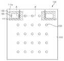
도 1은 본 발명의 일 실시예에 따른 발광소자를 설명하기 위한 평면도이다.
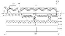
도 2는 도 1의 절취선 AA'를 따라 취해진 단면도이다.
도 3은 본 발명의 일 실시예에 따른 발광소자의 제조 방법을 설명하기 위한 단면도들이다.
도 4는 본 발명의 다른 실시예에 따른 발광소자를 설명하기 위한 평면도이다.
도 5a는 본 발명의 또 다른 실시예에 따른 발광소자를 설명하기 위한 평면도이다.
도 5b는 본 발명의 또 다른 실시예에 다른 발광소자의 라인전극이 배치된 것을 설명하기 위한 도면이다.
도 6은 도 5a의 절취선 BB'를 따라 취해진 단면도이다.
도 7은 본 발명의 일 실시예에 따른 발광소자를 조명 장치에 적용한 예를 설명하기 위한 분해 사시도이다.
도 8은 본 발명의 일 실시예에 따른 발광소자를 디스플레이 장치에 적용한 예를 설명하기 위한 단면도이다.
도 9는 본 발명의 일 실시예에 따른 발광소자를 디스플레이 장치에 적용한 예를 설명하기 위한 단면도이다.
도 10은 본 발명의 일 실시예에 따른 발광소자를 헤드 램프에 적용한 예를 설명하기 위한 단면도이다.1 is a plan view illustrating a light emitting device according to an embodiment of the present invention.
2 is a cross-sectional view taken along the perforated line AA 'of FIG.
3 is a cross-sectional view illustrating a method of manufacturing a light emitting device according to an embodiment of the present invention.
4 is a plan view illustrating a light emitting device according to another embodiment of the present invention.
5A is a plan view illustrating a light emitting device according to another embodiment of the present invention.
5B is a view for explaining the arrangement of line electrodes of another light emitting device according to another embodiment of the present invention.
FIG. 6 is a cross-sectional view taken along the percutaneous line BB 'of FIG. 5A.
7 is an exploded perspective view illustrating an example in which a light emitting device according to an embodiment of the present invention is applied to a lighting device.
8 is a cross-sectional view illustrating an example in which a light emitting device according to an embodiment of the present invention is applied to a display device.
9 is a cross-sectional view illustrating an example in which a light emitting device according to an embodiment of the present invention is applied to a display device.
10 is a cross-sectional view illustrating an example in which a light emitting device according to an embodiment of the present invention is applied to a headlamp.
본 발명의 바람직한 실시예에 대하여 첨부된 도면을 참조하여 더 구체적으로 설명한다.Preferred embodiments of the present invention will be described more specifically with reference to the accompanying drawings.
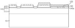
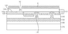
도 1은 본 발명의 일 실시예에 따른 발광소자를 설명하기 위한 평면도이고, 도 2는 도 1의 절취선 AA를 따라 취해진 단면도이다.FIG. 1 is a plan view for explaining a light emitting device according to an embodiment of the present invention, and FIG. 2 is a cross-sectional view taken along a perforated line AA in FIG.
도 1 및 도 2를 참조하면, 발광소자(100)는 발광구조체(110), 금속층(120, 130), 제1 절연층(140), 전극층(150), 본딩층(160), 기판(170), 전극패드(180) 및 보호층(190)을 포함할 수 있다.1 and 2, a
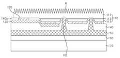
발광구조체(110)는 제1 도전형 반도체층(111), 활성층(113) 및 제2 도전형 반도체층(115)을 포함한다. 제1 도전형 반도체층(111)은 제2 도전형 반도체층(115)의 상부에 위치하고, 활성층(113)은 제1 도전형 반도체층(111)과 제2 도전형 반도체층(115) 사이에 개재될 수 있다. 그리고 본 발명의 일 실시예에서 제1 도전형 반도체층(111) 상부면에 러프니스(R)를 더 포함할 수 있으며, 러프니스(R) 하부에 복수의 하부 메사들이 형성될 수 있다.The
제1 도전형 반도체층(111)과 제2 도전형 반도체층(115)은 각각 III-V 계열의 화합물 반도체를 포함할 수 있는데, 일례로, (Al, Ga, In)N과 같은 질화물계 반도체를 포함할 수 있다. 그리고 제1 도전형 반도체층(111)은 Si와 같은 n형 불순물이 도핑된 n형 반도체층을 포함할 수 있으며, 제2 도전형 반도체층(115)은 Mg와 같은 p형 불순물이 도핑된 p형 반도체층을 포함할 수 있다. 이때, 제1 도전형 반도체층(111)과 제2 도전형 반도체층(115)의 불순물 도핑은 반대로 도핑될 수도 있다.The first
또한, 제1 도전형 반도체층(111)과 제2 도전형 반도체층(115)은 각각 단일층으로 형성될 수 있고, 다중층을 포함할 수도 있다. 일례로, 제1 도전형 반도체층(111) 및/또는 제2 도전형 반도체층(115)은 클래층 및 컨택층을 포함할 수 있고, 초격자층을 포함할 수도 있다.In addition, the first
활성층(113)은 다중양장우물 구조(MQW)를 포함할 수 있고, 다중양자우물구조에서 원하는 피크 파장의 빛을 방출할 수 있도록 다중양자우물구조의 원소와 조성비 등이 조정될 수 있다. 일례로, 활성층(113)의 우물층은 InGaN 등의 삼성분계 반도체층이거나 AlInGaN 등의 사성분계 반도체층일 수 있으며, 각 성분의 조성비를 조정하여 원하는 피크 파장의 빛이 방출되도록 할 수 있다.The
상기와 같은 발광구조체(110)의 일부를 제거하여 도 1 및 도 2에 도시된 바와 같이, 발광구조체(110)를 관통하는 제1 홈(H1)을 형성할 수 있다. 본 발명의 일 실시예에서 두 개의 제1 홈(H1)이 형성되며, 두 개의 제1 홈(H1)에 의해 모서리 부분의 두 개의 패드설치부(111a)가 발광구조체(110)와 구분되도록 형성된다.A part of the
도 1을 참조하면, 패드설치부(111a)는 제1 홈(H1)들에 의해 사각형 형상으로 형성되지만, 패드설치부(111a)의 형상은 필요에 따라 변형될 수 있다.1, the
패드설치부(111a)는 도 1에서와 같이, 발광소자(100)의 모서리 측에 각각 설치되고, 도 2를 참조하면, 발광구조체(110)와 동일한 높이로 형성될 수 있다. 패드설치부(111a)는 발광구조체(110)를 형성하는 과정에서 형성됨에 따라 발광구조체(110)의 제1 도전형 반도체층(111)과 동일한 조성을 가지는 반도체층으로 구성될 수 있다. 그리고 발광구조체(110)와 동일한 높이로 형성된다. 그에 따라 패드설치부(111a)에 설치된 전극패드(180)가 발광구조체(110)보다 돌출되어 설치됨에 따라 와이어 본딩 시 불량률을 낮출 수 있다.As shown in FIG. 1, the
러프니스(R)는 제1 도전형 반도체층(111) 상면에 형성될 수 있고, 불규칙한 요철을 포함할 수 있다. 이렇게 발광구조체(110) 상부면에 러프니스(R)를 형성함으로써, 발광구조체(110) 상부면을 통해 빛이 방출되는 광 추출 효율을 향상시킬 수 있다.The roughness R may be formed on the upper surface of the first conductivity
러프니스(R)의 형성은 KOH 및 NaOH 중 적어도 하나를 포함하는 용액을 이용하여 습식 식각하여 형성할 수 있고, 또는 PEC 식각을 이용하여 형성할 수도 있다. 또한, 러프니스(R)는 성장 기판이 제1 도전형 반도체층(111)에서 분리될 때, 자연적으로 형성될 수도 있다. 일례로, 화학적 리프트오프 또는 응력 리프트 오프를 이용하여 제1 도전형 반도체층(111)에서 성장 기판을 분리하는 경우, 성장 기판을 분리하기 위해 추가적으로 형성되는 희생층에 의해 형성된 공동으로부터 제1 도전형 반도체층(111)의 분리면에 러프니스(R)가 형성될 수 있다. 이 처럼 러프니스(R)는 다양한 방법으로 형성될 수 있다.Roughness (R) may be formed by wet etching using a solution containing at least one of KOH and NaOH, or may be formed using PEC etching. Further, the roughness R may be formed naturally when the growth substrate is separated from the first conductivity
발광구조체(110)의 하부에 메사가 형성될 수 있다. 메사는 제2 도전형 반도체층(115), 활성층(113)을 포함할 수 있으며, 제1 도전형 반도체층(111)의 일부를 더 포함할 수도 있다. 본 발명의 일 실시예에서 메사는 도 1 및 도 2에 도시된 바와 같이, 부분적으로 일부분이 다수 돌출 형성된 형상으로 형성될 수 있다. 이는 본 발명에 한정되는 것은 아니며, 메사는 다양한 형상 및 크기를 가질 수 있다.A mesa may be formed under the
또한, 메사에 하나 이상의 제2 홈(H2)이 형성될 수 있다. 그에 따라 전극층(150)이 제2 홈(H2)을 채워 전극층(150)과 제1 도전형 반도체층(111)이 전기적으로 접촉될 수 있다. 그리고 도 1에 도시된 바와 같이, 다수의 제2 홈(H2)은 일정 규칙을 따라 배열된 것으로 보이지만, 이는 필요에 따라 위치 및 배열이 다양하게 변경될 수 있다.Also, one or more second grooves H2 may be formed in the mesa. Accordingly, the
금속층(120, 130)은 발광구조체(110)의 하부에 형성되며, 반사금속층(120)과 커버금속층(130)을 포함한다. 금속층(120, 130)은 제2 도전형 반도체층(115)과 전기적으로 연결될 수 있으며, 본 발명의 일 실시예에서는 금속층(120, 130)과 제2 도전형 반도체층(115)이 직접 접촉된 것을 도면에 도시하였다.The metal layers 120 and 130 are formed under the
반사금속층(120)은 발광구조체(110)에서 발출된 빛을 반사하는 기능이 있으며, 본 발명의 일 실시예에서는 제2 도전형 반도체층(115)과 전기적으로 연결되는 전극 기능도 있다. 따라서 반사금속층(120)은 높은 반사도를 가지면서 제2 도전형 반도체층(115)과 오믹 접촉을 형성할 수 있는 금속을 포함할 수 있다. 그러므로 반사금속층(120)은 Ni, Pt, Pd, Rh, W, Ti, Al, Ag 및 Au 중 하나 이상을 포함할 수 있으며, 필요에 따라 단일층 또는 다중층으로 형성될 수 있다.The
또한, 반사금속층(120)은 단일층으로 형성된 경우에도, 도 2에 도시된 바와 같이, 전 영역에 반사금속층(120)을 형성하지 않고, 일부 영역에만 반사금속층(120)을 형성할 수 있다. 즉, 메사에서 경사면이 포함된 영역에는 반사금속층(120)을 형성하지 않고 제2 절연층(140a, 예컨대, SiO2)을 형성하며, 평평한 영역에만 반사금속층(120)을 형성할 수 있다. 이를 통해 반사금속층(120)이 제2 도전형 반도체층(115)의 면적보다 작은 면적을 갖도록 형성되며, 제2 홈(H2)을 채운 전극층(150)과 반사금속층(120)이 직접 접촉하지 않도록 한다. 여기서, 제2 절연층(140a)은 일례로, SiO2 또는 SiN을 포함할 수 있다.Also, even when the
이때, 반사금속층(120)은 제2 홈(H2)이 형성된 위치를 제외한 제2 도전형 반도체층(115)의 대부분 영역에 배치되어 활성층(113)에서 방출된 빛 중 아래를 향하는 빛은 대부분 반사금속층(120)에 도달하여 상부로 반사될 수 있다. 그에 따라 발광소자(100)의 광추출 효율이 향상될 수 있다.At this time, the
커버금속층(130)은 반사금속층(120)의 일부를 덮도록 형성된다. 도 2에 도시된 바와 같이, 커버금속층(130)은 전극패드(180)가 형성된 위치를 포함하여 반사금속층(120)의 일부를 덮는다. 종래에는 커버금속층(130)이 반사금속층(120) 전체를 덮도록 형성되어 반사금속층(120)과 커버금속층(130) 간의 메탈 스트레스(metal stress)가 반사금속층(120) 전체에 걸쳐 있었으나, 본 발명의 일 실시예에서는 커버금속층(130)이 반사금속층(120)의 일부만 덮도록 형성되어 커버금속층(130)과 반사금속층(120) 간의 메탈 스트레스를 최소화하여, 이로 인한 필링(peeling)을 최소화할 수 있으며, 반사 효율도 향상할 수 있다.The
커버금속층(130)은 반사금속층(120)과 전기적으로 연결되어, 제2 도전형 반도체층(115)과 전기적으로 연결될 수 있다. 이로 인해 커버금속층(130)은 반사금속층(120)과 함께 일정의 전극 역할을 할 수 있다. 커버금속층(130)은 Au, Ni, Ti, Cr, Pt, W, TiW 중 하나 이상을 포함할 수 있고, 단일층이나 다중층으로 형성될 수 있다.The
제1 절연층(140)은 발광구조체(110)의 아래에 위치한다. 특히, 하부 메사에 형성된 제2 홈(H2)의 주변을 감싸도록 형성된다. 제1 절연층(140)은 절연성 물질을 포함할 수 있다. 또한, 제1 절연층(140)은 다중층을 포함할 수 있고, 굴절률이 다른 물질이 교대로 적층된 분포브래그반사기(DBR)를 포함할 수 있다.The first insulating
상기와 같이, 제1 절연층(140)이 분포브래그반사기가 포함되므로, 제1 절연층(140)을 두께를 두껍게 형성함으로써, 단차를 최소화할 수 있다.As described above, since the first insulating
전극층(150)은 제1 절연층(140) 아래에 위치한다. 그리고 전극층(150) 일부에서 돌출된 제1 전극(150a)이 제2 홈(H2)을 관통하여 제1 도전형 반도체층(111)에 오믹 접촉될 수 있다. 그에 따라 전극층(150)을 통해 공급된 전류는 제1 전극(150a)을 통해 제1 도전형 반도체층(111)에 공급될 수 있다.The
제1 전극(150a)은 전극층(150)에서 돌출되어 연장된 형상으로 형성되며, 다수 개가 형성될 수 있다. 또한, 다수의 제1 전극(150a)은 전극층(150) 전체에 배열되며, 배열되는 패턴은 도 1에 도시된 바와 같이, 배열될 수 있고, 필요에 따라 다양하게 변형될 수 있다. 이렇게 다수의 제1 전극(150a)을 발광소자(100) 전체에 걸쳐 배열함으로써, 전류 분산 효과가 더욱 향상될 수 있다.The
본딩층(160)은 전극층(150) 아래에 위치하여, 기판(170)을 전극층(150)에 본딩시킨다. 즉, 본딩층(160)을 통해 기판(170)이 발광구조체(110)에 본딩된다. 또한, 본딩층(160)은 전극층(150)에 형성된 제1 전극(150a)과 전기적으로 연결될 수 있으며, 기판(170)과 전극층(150)을 전기적으로 연결하는 기능을 할 수 있다. 이를 위해 본딩층(160)은 Au 및 Sn이 포함될 수 있으며, NiSn 또는 AuIn이 포함될 수도 있다.The
기판(170)은 본딩층(160) 아래에 위치할 수 있으며 외부의 전원이 공급되어 전극층(150) 및 제1 도전형 반도체층(111)으로 전원을 공급할 수 있다.The
또한, 기판(170)은 지지기판으로 역할을 수행할 수 있어, 도전성 기판, 회로기판, 도전 패턴이 형성된 절연기판일 수 있다. 본 발명의 일 실시예에서 기판은 금속이 포함될 수 있고, Mo층과 Cu층이 적층된 구조로 형성될 수 있다. 그리고 Ti, Cr, Ni, Al, Cu, Ag, Au, Pt 등이 포함될 수도 있다.In addition, the
전극패드(180)는 다수 개가 구비되어 패드설치부(111a) 상부에 각각 형성될 수 있다. 전극패드(180)는 러프니스(R)가 형성된 패드설치부(111a)의 상부에 형성되어 제1 도전형 반도체층(111)과 전기적으로 연결될 수 있다.A plurality of
또한, 전극패드(180)는 다수의 전극 패드층을 포함할 수 있으며, 상부 전극 패드층과 하부 전극 패드층을 포함할 수 있다. 하부 전극 패드층은 러프니스(R)가 형성된 제1 도전형 반도체에 증착되어 형성되며, 하부 전극 패드층 상부에 상부 전극 패드층이 형성될 수 있다.In addition, the
상기와 같은 수직형 구조로 형성된 본 발명의 일 실시예에 따른 발광소자(100)에서 도 2에 도시된 바와 같이, 보호층(190)이 더 구비될 수 있다. 보호층(190)은 제1 도전형 반도체층(111)의 상면을 덮을 수 있다. 또한, 제1 도전형 반도체층(111)의 측면을 덮어 발광구조체(110)를 외부로부터 보호할 수 있고, 또한, 제1 도전형 반도체층(111) 상면의 러프니스(R)의 경사보다 완만한 경사를 갖도록 러프니스(R)를 덮어, 광 추출 효율을 향상시킬 수 있다. 이때, 보호층(190)은 절연성 물질을 포함할 수 있으며, 일례로, SiO2를 포함할 수 있다.In the
도 3은 본 발명의 일 실시예에 따른 발광소자의 제조 방법을 설명하기 위한 단면도들이다.3 is a cross-sectional view illustrating a method of manufacturing a light emitting device according to an embodiment of the present invention.
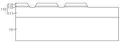
도 3a를 참조하면, 제1 도전형 반도체층(111), 활성층(113) 및 제2 도전형 반도체층(115)을 포함하는 발광구조체(110)를 형성한다.Referring to FIG. 3A, a
이때, 발광구조체(110)는 성장 기판(10) 상에 성장시키며, 성장 기판(10)은 발광구조체(110)를 성장시킬 수 있는 기판이면 어떤 기판이 이용되든 무관하다. 일례로, 사파이어 기판, 실리콘 카바이트 기판, 실리콘 기판, 질화갈륨 기판, 질화알루미늄 기판 등일 수 있다.At this time, the
그리고 제1 도전형 반도체층(111), 활성층(113), 제2 도전형 반도체층(115)은 MOCVD(metal organic chemical vapor deposition), MBE(molecular beam epitaxy) 또는 HVPE(hydride vapor epitaxy) 등의 기술을 이용하여 성장 기판(10) 상에 성장될 수 있다.The first conductivity
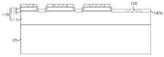
도 3b를 참조하면, 상기와 같이, 발광구조체(110)가 형성된 상태에서 발광구조체(110)의 상부에 일부를 식각하여 하부 메사 구조를 형성한다. 이때, 식각을 통해 제1 도전형 반도체층(111)의 일부가 노출될 수 있다.Referring to FIG. 3B, a portion of the upper portion of the
도 3c를 참조하면, 하부 메사가 형성된 발광구조체(110)의 상면에 반사금속층(120)을 증착시킨다. 이때, 반사금속층(120)은 발광구조체(110) 상면 전체에 형성하지 않고, 평평한 영역의 일부에 형성한다. 반사금속층(120)은 증착 등의 기술을 이용하여 제2 도전형 반도체층(115) 상에 형성되며, 리프트 오프 기술 등을 이용하여 원하는 부분에만 형성할 수 있으므로, 경사진 부분을 제외한 평평한 영역 전체에 형성한다. 그에 따라 반사금속층(120)은 제2 도전형 반도체층(115)이 노출된 영역보다 작은 크기로 형성될 수 있지만, 제2 도전형 반도체층(115)의 거의 대부분을 덮도록 형성될 수 있다. 그리고 반사금속층(120)이 형성되지 않은 영역에는 제2 절연층(140a)이 증착된다.Referring to FIG. 3C, a
도 3d를 참조하면, 반사금속층(120)이 형성된 상부에 커버금속층(130)이 증착된다. 커버금속층(130)은 반사금속층(120)의 일부를 덮도록 형성된다.Referring to FIG. 3D, a
도 3e를 참조하면, 제1 절연층(140)은 커버금속층(130) 상부 및 커버금속층(130)이 형성되지 않은 반사금속층(120) 전체를 덮도록 형성된다. 그리고 발광구조체(110)의 식각된 위치에 제2 홈(H2)을 형성한다. 그에 따라 제2 홉(H2)의 저면에 제1 도전형 반도체층(111)이 노출될 수 있다. 상기와 같이, 형성된 제2 홈(H2)은 다수 개가 형성될 수 있다.Referring to FIG. 3E, the first insulating
도 3f를 참조하면, 제1 절연층(140) 상부에 전극층(150)이 형성된다. 이때, 전극층(150)은 제1 절연층(140)에 형성된 제2 홈(H2)을 채워 제2 홈(H2)의 저면에 노출된 제1 도전형 반도체층(111)과 접촉될 수 있다.Referring to FIG. 3F, an
도 3g를 참조하면, 전극층(150) 상부에 본딩층(160)이 형성되고, 본딩층(160) 상부에 기판(170)이 차례로 형성될 수 있다. 이때, 성장 기판(10)은 기판(170)이 형성되면서 분리 제거될 수 있다. 그리고 본딩층(160)은 전극층(150)과 오믹 접촉되도록 형성될 수 있다. 본딩층(160)은 전극층(150)과 기판(170)의 사이에 개재한 상태에서 압력과 온도를 조절하여 전극층(150)과 기판(170)을 본딩시킨다.Referring to FIG. 3G, a
도 3h 내지 도 3j는 도 3a 내지 도 3g에 도시된 것들과 비교하여 상하가 반대로 도시되어 있다. 그러므로 상하 개념은 도 3h 내지 도 3j에 도시된 것을 기준을 설명하며, 이는 설명의 편의를 위한 것으로 본 발명을 제한하는 것은 아니다.3H to 3J are shown upside down in comparison with those shown in Figs. 3A to 3G. Therefore, the up-and-down concept will explain the criteria shown in Figs. 3h to 3j, which are for convenience of description and do not limit the present invention.
도 3h를 참조하면, 성장 기판(10)을 제거하면서 제1 도전형 반도체층(111)의 표면에 러프니스(R)가 형성될 수 있다. 또한, 성장 기판(10)이 제거되면서 발광구조체(110)의 측면 일부도 같이 제거될 수 있다.Referring to FIG. 3H, the roughness R may be formed on the surface of the first conductivity
도 3i를 참조하면, 상기와 같이, 성장 기판(10)이 제거된 상태에서 기판(170)이 본딩된 발광구조체(110)의 배면에 발광구조체(110)의 일부분을 제거하여, 발광구조체(110)를 관통하는 제1 홈(H1)을 형성한다. 제1 홈(H1)은 발광구조체(110)와 패드설치부(111a)를 분리하기 위한 것으로, 건식 식각 등을 통해 제1 도전형 반도체층(111), 활성층(113) 및 제2 도전형 반도체층(115)을 제거하여 형성될 수 있다. 이때, 발광구조체(110)에서 분리된 패드설치부(111a)는 도 3i에 도시된 바와 같이, 제1 도전형 반도체층(111)만 남은 상태로 형성될 수 있다.3I, a portion of the
또한, 제1 홈(H1)을 형성한 다음, 제1 도전형 반도체층(111) 상부에 보호층(190)을 추가로 형성할 수 있다. 보호층(190)은 제1 도전형 반도체층(111) 상부와 측면 그리고 제1 홈(H1)을 포함하는 전체에 형성될 수 있다. 그에 따라 발광구조체(110)를 외부에서 보호할 수 있으며, 제1 도전형 반도체층(111) 상부에 형성된 러프니스(R)의 경사를 완만하게 할 수 있어, 광 추출 효율을 향상시킬 수 있다.In addition, a
도 3j를 참조하면, 제1 홈(H1)에 의해 발광구조체(110)와 패드설치부(111a)로 구분된 상태에서, 패드설치부(111a) 상부면에 전극패드(180)를 형성한다. 전극패드(180)는 증착이나 리프트 오프 기술을 통해 형성될 수 있다. 이때, 전극패드(180)는 보호층(190) 일부가 제거된 상태에서 전극패드(180)와 패드설치부(111a)가 접촉할 수 있도록 설치된다.Referring to FIG. 3J, the
도 4는 본 발명의 다른 실시예에 따른 발광소자를 설명하기 위한 평면도이다.4 is a plan view illustrating a light emitting device according to another embodiment of the present invention.
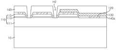
본 발명의 다른 실시예에 따른 발광소자(100)는 발광구조체(110), 금속층(120, 130), 제1 절연층(140), 전극층(150), 본딩층(160), 기판(170) 및 전극패드(180)를 포함하고, 보호층(190)을 더 포함할 수 있다. 본 발명의 다른 실시예에 따른 발광소자(100)에 대한 설명을 하면서, 일 실시예에서와 동일한 구성에 대한 설명은 생략하되, 필요에 따라 도 1 내지 도 3에 도시된 도면을 참조한다.A
도 4에 도시된 바와 같이, 본 발명의 다른 실시예에서 커버금속층(130)은 전극패드(180)가 형성된 위치와 더불어 발광구조체(110)의 테두리를 따라 형성된다. 그리고 커버금속층(130)은 반사금속층(120)의 테두리 부분을 모두 덮도록 형성되므로, 반사금속층(120)이 외부로 드러나지 않도록 한다. 그에 따라 반사금속층(120)이 노출됨에 따라 반사금속층(120)에 외부의 다른 물질이 확산되어 반사금속층(120)이 손상되는 것을 방지할 수 있다.4, in another embodiment of the present invention, the
도 5a는 본 발명의 또 다른 실시예에 따른 발광소자를 설명하기 위한 평면도이고, 도 5b는 본 발명의 또 다른 실시예에 다른 발광소자의 라인전극이 배치된 것을 설명하기 위한 도면이다. 그리고 도 6은 도 5a의 절취선 BB'를 따라 취해진 단면도이다.FIG. 5A is a plan view illustrating a light emitting device according to another embodiment of the present invention, and FIG. 5B is a view illustrating a layout of line electrodes of another light emitting device according to another embodiment of the present invention. And FIG. 6 is a cross-sectional view taken along the percutaneous line BB 'of FIG. 5A.
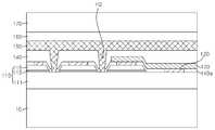
본 발명의 또 다른 실시예에 따른 발광소자(100)는 발광구조체(110), 금속층(120, 130), 제1 절연층(140), 제2 절연층(140a), 전극층(150), 본딩층(160), 기판(170), 전극패드(180) 및 보호층(190)을 포함한다. 본 발명의 또 다른 실시예에 따른 발광소자(100)를 설명하면서 필요에 따라 도 1 내지 도 3을 참조하여 설명하되, 일 실시예에서와 동일한 설명은 생략한다.A
본 발명의 또 다른 실시예에서 발광소자(100)는 도 5a 및 도 5b에 도시된 바와 같이, 다수의 제2 홈(H2)이 형성되되, 다수의 제2 홈(H2)은 규칙적 또는 불규칙적으로 배치될 수 있다. 그리고 발광소자(100)의 모서리 측에는 두 개의 전극패드(180)가 각각 배치될 수 있다. 발광소자(100)의 일부를 제외한 전체에 반사금속층(120) 및 커버금속층(130)이 덮여 형성될 수 있다.In another embodiment of the present invention, as shown in FIGS. 5A and 5B, the
또한, 본 발명의 또 다른 실시예에서 발광소자(100)의 테두리를 따라 라인 전극(150b)이 형성될 수 있다. 라인 전극(150b)은 전극패드(180)가 형성된 위치를 제외한 발광소자(100)의 테두리 전체를 둘러싸도록 형성된다. 즉, 도 5b에 도시된 평면도에서 두 개의 전극패드(180)가 발광소자(100)의 위쪽 모서리 측에 각각 배치된 상태에서 라인 전극(150b)은 두 개의 전극패드(180) 사이와 발광소자(100)의 다른 테두리를 따라 형성될 수 있다.Further, in another embodiment of the present invention, the
그리고 도 5a에 도시된 바와 같이, 전극패드(180)가 형성된 위치를 제외한 전체 영역에서 커버금속층(130)은 반사금속층(120)보다 안쪽에 형성될 수 있다. 즉, 반사금속층(120)이 커버금속층(130)보다 발광소자(100)의 전체 영역에서 넓게 형성됨에 따라 발광소자(100)의 반사효율을 높여 발광소자(100)의 발광효율을 보다 높일 수 있다. 이때, 커버금속층(130)은 전극패드(180)와 제2 도전형 반도체층(115)을 전기적으로 연결시키기 위해 전극패드(180) 하부까지 연장되어 형성될 수 있다.As shown in FIG. 5A, the
또한, 라인전극(150b)은 반사금속층(120) 및 커버금속층(130)보다 발광소자(100)의 외측에 형성될 수 있다. 그리고 라인전극(150b)의 외측까지 제1 절연층(140)이 형성됨에 따라 발광소자(100)의 측면을 보호할 수 있다.The
상기와 같은 발광소자(100)의 세부 구조에 대해 도 6을 참조하여 설명한다. 도 6을 참조하면, 기판(170) 상부에 본딩층(160)이 형성되고, 본딩층(160)에 의해 전극층(150)이 기판(170)과 결합된다. 전극층(150) 상부에 제1 절연층(140)이 형성되고, 제1 절연층(140) 상부에 커버금속층(130)과 반사금속층(120)을 포함하는 금속층(120, 130)이 차례로 적층된다. 그리고 반사금속층(120)의 측면에 제2 절연층(140a)이 형성된다. 이때, 제2 절연층(140a)은 반사금속층(120) 및 커버금속층(130)의 전체 두께보다 두껍게 형성될 수 있으며, 이에 대해서는 후술한다.The detailed structure of the
제2 절연층(140a) 및 반사금속층(120)의 상부에 발광구조체(110)가 배치되고, 발광구조체(110)는 다수의 메사를 포함하고, 다수의 메사 사이에 제2 홈(H2) 및 제3 홈(H3)이 형성된다. 제2 홈(H2) 및 제3 홈(H3)은 제1 절연층(140)를 관통하여 제1 도전형 반도체층(111)이 노출되도록 형성된다. 그리고 전극층(150)이 제2 홈(H2) 및 제3 홈(H3)을 채워 전극층(150)과 제1 도전형 반도체층(111)이 전기적으로 접촉될 수 있다. 이때, 제2 홈(H2) 및 제3 홈(H3)의 측면은 제1 절연층(140)에 의해 덮혀 제2 홈(H2) 및 제3 홈(H3)을 채운 전극층(150)이 다른 층과 전기적으로 절연될 수 있도록 한다.A
여기서, 제2 홈(H2)은 도 1에 도시된 바와 같이, 평면 형상이 원형 등과 같은 형상으로 형성되며, 제3 홈(H3)은 평면 형상이 일 방향으로 길이를 갖는 라인 형상으로 형성된다. 그에 따라 제2 홈(H2)을 채운 전극층(150)의 구조와 제3 홈(H3)을 채운 전극층(150)의 구조가 서로 달라진다. 이때, 제2 홈(H2)을 채운 전극층(150)을 제1 전극(150a)이라 하고, 제3 홈(H3)을 채운 전극층(150)을 라인 전극(150b)이라 한다.Here, as shown in FIG. 1, the second groove H2 is formed in a planar shape such as a circular shape, and the third groove H3 is formed in a line shape having a planar shape in one direction. The structure of the
제1 전극(150a)은 도 1에 도시된 바와 같이, 발광소자(100)의 전체 면에 걸쳐 부분적으로 다수 개가 분포될 수 있으며, 분포 배치는 규칙적 또는 불규칙적으로 배치될 수 있다.As shown in FIG. 1, the
본 발명의 또 다른 실시예에서 라인 전극(150b)은 발광소자(100)의 테두리를 따라 방향성을 가지는 라인 형상으로 형성되고, 전극패드(180)가 배치되는 발광소자(100)의 모서리 측에만 형성되지 않는다. 물론, 라인 전극(150b)의 형상은 일 방향의 방향성을 갖는 라인 형상이 아닌 곡선의 형상으로 형성될 수도 있고, 전극패드(180)가 형성된 위치에도 필요에 따라 형성될 수도 있다.The
상기와 같이, 라인 전극(150b)이 발광소자(100)의 테두리에 형성됨에 따라 발광소자(100)의 전류 스프레딩이 발광소자(100)의 평면 형상의 중앙에 집중되면서 상대적으로 발광소자(100)의 테두리 측의 발광효율이 떨어지는 것을 방지할 수 있다. 즉, 라인 전극(150b)이 발광소자(100)의 테두리를 따라 형성됨에 따라 발광소자(100)의 테두리 측의 발광효율을 높일 수 있다. 그렇기 때문에 발광소자(100)의 전체에서 발광이 균일할 수 있어 발광효율이 향상될 수 있다.The current spreading of the
또한, 본 발명의 또 다른 실시예에서 라인 전극(150b)은 전극패드(180)가 형성되지 않은 발광소자(100)의 모서리 측에 모서리의 형상을 따라 연속적으로 형성되어 발광소자(100)의 끝단의 발광효율을 높일 수 있다.In another embodiment of the present invention, the
그리고 라인 전극(150b)의 외측에는 금속층(120, 130)이 형성되지 않는다. 라인 전극(150b)의 외측은 도 2에서 라인 전극(150b)의 왼쪽이며, 라인 전극(150b)의 외측에는 제1 절연층(140)만 형성된다.The metal layers 120 and 130 are not formed on the outside of the
도 6을 참조하면, 제2 홈(H2)을 채운 제1 전극(150a)의 너비(d1)와 제3 홈(H3)을 채운 라인 전극(150b)의 너비(d2)는 동일하지 않고, 라인 전극(150b)의 너비(d2)는 제1 전극(150a)의 너비(d1)보다 얇게 형성된다. 라인 전극(150b)은 발광소자(100)의 테두리 측을 따라 형성되고, 제1 전극(150a)들이 배치된 분포와 별도로 형성된다. 그렇기 때문에 라인 전극(150b)의 너비(d2)를 제1 전극(150a)보다 얇게 형성하여 라인 전극(150b)의 전류 스프레딩이 제1 전극(150a)에서 보다 약하게 이루어지도록 할 수 있다.6, the width d1 of the
또한, 제1 전극(150a)이 제1 도전형 반도체층(111)에 컨택되는 너비(d3)와 라인 전극(150b)이 제1 도전형 반도체층(111)에 컨택되는 너비(d4)도 서로 다르게 형성되며, 라인 전극(150b)이 제1 도전형 반도체층(111)에 컨택되는 너비(d4)가 제1 전극(150a)의 너비(d3)보다 얇게 형성된다.The width d3 of the
그리고 일 실시예에서와 같이, 제1 절연층(140)은 제2 홈(H2) 및 제3 홈(H3)이 형성된 위치를 제외한 전체에 형성되고, 제2 절연층(140a)은 반사금속층(120)의 양 측에 각각 형성된다. 이때, 제2 절연층(140a)의 두께(d6)는 반사금속층(120)의 두께(d5)보다 두껍게 형성되며, 반사금속층(120)의 두께(d5)와 반사금속층(120)을 덮는 커버금속층(130)의 두께(d8)를 합친 두께(d5 + d8)보다 두껍게 형성된다. 본 발명의 또 다른 실시예에서 반사금속층(120)의 두께(d5)는 예컨대 약 2200Å의 두께로 형성되고, 커버금속층(130)의 두께(d8)는 약 7000Å의 두께로 형성된다. 그리고 반사금속층(120)의 양측에 형성된 제2 절연층(140a)의 두께(d6)는 약 16000Å의 두께로 형성된다.The first insulating
또한, 본 발명의 또 다른 실시예에서 전극패드(180)는 도 1에 도시된 바와 같이, 발광소자(100)의 모서리 측에 형성된다. 그리고 도 2에 도시된 바와 같이, 전극패드(180)가 배치되는 위치에 발광구조체(110)를 식각하여 제거한 상태에서 전극패드(180)가 형성된다. 전극패드(180)가 설치되는 위치의 수직 구조를 살펴보면, 전극층(150) 상부에 제1 절연층(140)이 형성되고, 제1 절연층(140) 상부에 커버금속층(130)이 형성된다. 그리고 커버금속층(130)의 상부에 제2 절연층(140a)이 형성된다.In addition, in another embodiment of the present invention, the
이때, 커버금속층(130)은 발광구조체(110)의 하부에 형성된 위치에서 연장되어 동일한 두께(d8)로 형성된다. 그리고 커버금속층(130)의 상부에 형성된 제2 절연층(140a)도 발광구조체(110)의 하부에 형성된 제2 절연층(140a)에서 연장되어 형성되되, 발광구조체(110)의 하부에서의 두께(d6)보다 얇은 두께(d7)를 가지도록 형성된다. 본 발명의 또 다른 실시예에서 발광구조체(110)의 하부에 형성된 제2 절연층(140a)의 두께(d6)는 약 16000Å로 형성되고, 전극패드(180)가 배치되는 위치의 제2 절연층(140a)의 두께(d7)는 약 8000Å로 형성된다.At this time, the
상기와 같이, 발광구조체(110)의 하부에 배치된 제2 절연층(140a)의 두께(d6)가 전극패드(180)의 하부에 배치된 제2 절연층(140a)의 두께(d7) 보다 두껍게 형성된 것은 제2 도전형 반도체와 전극층(150) 간의 전기적 절연이 잘 이루어지도록 하기 위함이다. 이는 최근 발광소자(100)가 고전류 및 고전압이 인가됨에 따라 발광구조체(110)와 전극층(150) 사이의 절연이 더욱 중요한 요인으로 작용할 수 있다.The thickness d6 of the second insulating
또한, 전극패드(180)가 형성된 위치에는 발광구조체(110)가 형성되지 않기 때문에 제2 절연층(140a)의 두께를 발광구조체(110)의 아래에서와 같이 두껍게 형성하지 않아도 된다. 단순히 제2 절연층(140a)의 두께를 두껍게 하는 것은 절연 기능은 높아질 수 있지만, 발광 영역이 위치하는 발광구조체(110)의 두께가 상대적으로 감소할 수 있어, 발광소자(100)의 발광 효율을 감소시키는 역효과가 나올 수 있다.In addition, since the
그리고 커버금속층(130)이 발광구조체(110)의 하부에서 연장되어 전극패드(180)가 형성된 위치까지 연장되어 형성됨에 따라 반사면적이 커지기 때문에 발광소자(100)의 발광효율을 높일 수 있다.Since the
그리고 전극패드(180)는 발광구조체(110)가 제거된 위치에 형성되며, 도 2에 도시된 바와 같이, 제2 절연층(140a)의 일부가 제거되어 전극패드(180)는 커버금속층(130)과 접촉된 상태로 형성된다.The
그리고 보호층(190)은 발광구조체(110) 전체를 덮도록 형성되며, 전극패드(180)를 제외한 발광소자(100) 전체에 형성될 수 있다.
The
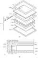
도 7은 본 발명의 일 실시예에 따른 발광소자를 조명 장치에 적용한 예를 설명하기 위한 분해 사시도이다.7 is an exploded perspective view illustrating an example in which a light emitting device according to an embodiment of the present invention is applied to a lighting device.
도 7을 참조하면, 본 실시예에 따른 조명 장치는, 확산 커버(1010), 발광소자 모듈(1020) 및 바디부(1030)를 포함한다. 바디부(1030)는 발광소자 모듈(1020)을 수용할 수 있고, 확산 커버(1010)는 발광소자 모듈(1020)의 상부를 커버할 수 있도록 바디부(1030) 상에 배치될 수 있다.Referring to FIG. 7, the illumination device according to the present embodiment includes a
바디부(1030)는 발광소자 모듈(1020)을 수용 및 지지하여, 발광소자 모듈(1020)에 전기적 전원을 공급할 수 있는 형태이면 제한되지 않는다. 예를 들어, 도시된 바와 같이, 바디부(1030)는 바디 케이스(1031), 전원 공급 장치(1033), 전원 케이스(1035), 및 전원 접속부(1037)를 포함할 수 있다.The
전원 공급 장치(1033)는 전원 케이스(1035) 내에 수용되어 발광소자 모듈(1020)과 전기적으로 연결되며, 적어도 하나의 IC칩을 포함할 수 있다. 상기 IC칩은 발광소자 모듈(1020)로 공급되는 전원의 특성을 조절, 변환 또는 제어할 수 있다. 전원 케이스(1035)는 전원 공급 장치(1033)를 수용하여 지지할 수 있고, 전원 공급 장치(1033)가 그 내부에 고정된 전원 케이스(1035)는 바디 케이스(1031)의 내부에 위치할 수 있다. 전원 접속부(115)는 전원 케이스(1035)의 하단에 배치되어, 전원 케이스(1035)와 결속될 수 있다. 이에 따라, 전원 접속부(115)는 전원 케이스(1035) 내부의 전원 공급 장치(1033)와 전기적으로 연결되어, 외부 전원이 전원 공급 장치(1033)에 공급될 수 있는 통로 역할을 할 수 있다.The
발광소자 모듈(1020)은 기판(1023) 및 기판(1023) 상에 배치된 발광소자(1021)를 포함한다. 발광소자 모듈(1020)은 바디 케이스(1031) 상부에 마련되어 전원 공급 장치(1033)에 전기적으로 연결될 수 있다.The light emitting
기판(1023)은 발광소자(1021)를 지지할 수 있는 기판이면 제한되지 않으며, 예를 들어, 배선을 포함하는 인쇄회로기판일 수 있다. 기판(1023)은 바디 케이스(1031)에 안정적으로 고정될 수 있도록, 바디 케이스(1031) 상부의 고정부에 대응하는 형태를 가질 수 있다. 발광소자(1021)는 상술한 본 발명의 실시예들에 따른 발광소자들 중 적어도 하나를 포함할 수 있다.The
확산 커버(1010)는 발광소자(1021) 상에 배치되되, 바디 케이스(1031)에 고정되어 발광소자(1021)를 커버할 수 있다. 확산 커버(1010)는 투광성 재질을 가질 수 있으며, 확산 커버(1010)의 형태 및 광 투과성을 조절하여 조명 장치의 지향 특성을 조절할 수 있다. 따라서 확산 커버(1010)는 조명 장치의 이용 목적 및 적용 태양에 따라 다양한 형태로 변형될 수 있다.The
도 8은 본 발명의 일 실시예에 따른 발광소자를 디스플레이 장치에 적용한 예를 설명하기 위한 단면도이다.8 is a cross-sectional view illustrating an example in which a light emitting device according to an embodiment of the present invention is applied to a display device.
본 실시예의 디스플레이 장치는 표시패널(2110), 표시패널(2110)에 광을 제공하는 백라이트 유닛(BLU1) 및, 상기 표시패널(2110)의 하부 가장자리를 지지하는 패널 가이드(2100)를 포함한다.The display device of this embodiment includes a
표시패널(2110)은 특별히 한정되지 않고, 예컨대, 액정층을 포함하는 액정표시패널일 수 있다. 표시패널(2110)의 가장자리에는 상기 게이트 라인으로 구동신호를 공급하는 게이트 구동 PCB가 더 위치할 수 있다. 여기서, 게이트 구동 PCB(2112, 2113)는 별도의 PCB에 구성되지 않고, 박막 트랜지스터 기판상에 형성될 수도 있다.The
백라이트 유닛(BLU1)은 적어도 하나의 기판(2150) 및 복수의 발광소자(2160)를 포함하는 광원 모듈을 포함한다. 나아가, 백라이트 유닛(BLU1)은 바텀커버(2180), 반사 시트(2170), 확산 플레이트(2131) 및 광학 시트들(2130)을 더 포함할 수 있다.The backlight unit (BLU1) includes a light source module including at least one substrate (2150) and a plurality of light emitting elements (2160). Further, the backlight unit BLU1 may further include a
바텀커버(2180)는 상부로 개구되어, 기판(2150), 발광소자(2160), 반사 시트(2170), 확산 플레이트(2131) 및 광학 시트들(2130)을 수납할 수 있다. 또한, 바텀커버(2180)는 패널 가이드(2100)와 결합될 수 있다. 기판(2150)은 반사 시트(2170)의 하부에 위치하여, 반사 시트(2170)에 둘러싸인 형태로 배치될 수 있다. 다만, 이에 한정되지 않고, 반사 물질이 표면에 코팅된 경우에는 반사 시트(2170) 상에 위치할 수도 있다. 또한, 기판(2150)은 복수로 형성되어, 복수의 기판(2150)들이 나란히 배치된 형태로 배치될 수 있으나, 이에 한정되지 않고, 단일의 기판(2150)으로 형성될 수도 있다.The
발광소자(2160)는 상술한 본 발명의 실시예들에 따른 발광소자들 중 적어도 하나를 포함할 수 있다. 발광소자(2160)들은 기판(2150) 상에 일정한 패턴으로 규칙적으로 배열될 수 있다. 또한, 각각의 발광소자(2160) 상에는 렌즈(2210)가 배치되어, 복수의 발광소자(2160)들로부터 방출되는 광을 균일성을 향상시킬 수 있다.The
확산 플레이트(2131) 및 광학 시트들(2130)은 발광소자(2160) 상에 위치한다. 발광소자(2160)로부터 방출된 광은 확산 플레이트(2131) 및 광학 시트들(2130)을 거쳐 면 광원 형태로 표시패널(2110)로 공급될 수 있다.The
이와 같이, 본 발명의 실시예들에 따른 발광소자는 본 실시예와 같은 직하형 디스플레이 장치에 적용될 수 있다.As described above, the light emitting device according to the embodiments of the present invention can be applied to the direct-type display device as in the present embodiment.
도 9는 일 실시예에 따른 발광소자를 디스플레이 장치에 적용한 예를 설명하기 위한 단면도이다.9 is a cross-sectional view illustrating an example in which a light emitting device according to an embodiment is applied to a display device.
본 실시예에 따른 백라이트 유닛이 구비된 디스플레이 장치는 영상이 디스플레이되는 표시패널(3210), 표시패널(3210)의 배면에 배치되어 광을 조사하는 백라이트 유닛(BLU2)을 포함한다. 나아가, 상기 디스플레이 장치는, 표시패널(3210)을 지지하고 백라이트 유닛(BLU2)이 수납되는 프레임(240) 및 상기 표시패널(3210)을 감싸는 커버(3240, 3280)를 포함한다.The display device having the backlight unit according to the present embodiment includes a
표시패널(3210)은 특별히 한정되지 않고, 예컨대, 액정층을 포함하는 액정표시패널일 수 있다. 표시패널(3210)의 가장자리에는 상기 게이트 라인으로 구동신호를 공급하는 게이트 구동 PCB가 더 위치할 수 있다. 여기서, 게이트 구동 PCB는 별도의 PCB에 구성되지 않고, 박막 트랜지스터 기판상에 형성될 수도 있다. 표시패널(3210)은 그 상하부에 위치하는 커버(3240, 3280)에 의해 고정되며, 하부에 위치하는 커버(3280)는 백라이트 유닛(BLU2)과 결속될 수 있다.The
표시패널(3210)에 광을 제공하는 백라이트 유닛(BLU2)은 상면의 일부가 개구된 하부 커버(3270), 하부 커버(3270)의 내부 일 측에 배치된 광원 모듈 및 상기 광원 모듈과 나란하게 위치되어 점광을 면광으로 변환하는 도광판(3250)을 포함한다. 또한, 본 실시예의 백라이트 유닛(BLU2)은 도광판(3250) 상에 위치되어 광을 확산 및 집광시키는 광학 시트들(3230), 도광판(3250)의 하부에 배치되어 도광판(3250)의 하부방향으로 진행하는 광을 표시패널(3210) 방향으로 반사시키는 반사시트(3260)를 더 포함할 수 있다.The backlight unit BLU2 for providing light to the
광원 모듈은 기판(3220) 및 상기 기판(3220)의 일면에 일정 간격으로 이격되어 배치된 복수의 발광소자(3110)를 포함한다. 기판(3220)은 발광소자(3110)를 지지하고 발광소자(3110)에 전기적으로 연결된 것이면 제한되지 않으며, 예컨대, 인쇄회로기판일 수 있다. 발광소자(3110)는 상술한 본 발명의 실시예들에 따른 발광소자를 적어도 하나 포함할 수 있다. 광원 모듈로부터 방출된 광은 도광판(3250)으로 입사되어 광학 시트들(3230)을 통해 표시패널(3210)로 공급된다. 도광판(3250) 및 광학 시트들(3230)을 통해, 발광소자(3110)들로부터 방출된 점 광원이 면 광원으로 변형될 수 있다.The light source module includes a
이와 같이, 본 발명의 실시예들에 따른 발광소자는 본 실시예와 같은 에지형 디스플레이 장치에 적용될 수 있다.As described above, the light emitting device according to the embodiments of the present invention can be applied to the edge display device as in the present embodiment.
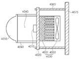
도 10은 본 발명의 일 실시예에 따른 발광소자를 헤드 램프에 적용한 예를 설명하기 위한 단면도이다.10 is a cross-sectional view illustrating an example in which a light emitting device according to an embodiment of the present invention is applied to a headlamp.
도 10을 참조하면, 상기 헤드 램프는, 램프 바디(4070), 기판(4020), 발광소자(4010) 및 커버 렌즈(4050)를 포함한다. 나아가, 상기 헤드 램프는, 방열부(4030), 지지랙(4060) 및 연결 부재(4040)를 더 포함할 수 있다.Referring to FIG. 10, the head lamp includes a
기판(4020)은 지지랙(4060)에 의해 고정되어 램프 바디(4070) 상에 이격 배치된다. 기판(4020)은 발광소자(4010)를 지지할 수 있는 기판이면 제한되지 않으며, 예컨대, 인쇄회로기판과 같은 도전 패턴을 갖는 기판일 수 있다. 발광소자(4010)는 기판(4020) 상에 위치하며, 기판(4020)에 의해 지지 및 고정될 수 있다. 또한, 기판(4020)의 도전 패턴을 통해 발광소자(4010)는 외부의 전원과 전기적으로 연결될 수 있다. 또한, 발광소자(4010)는 상술한 본 발명의 실시예들에 따른 발광소자를 적어도 하나 포함할 수 있다.
커버 렌즈(4050)는 발광소자(4010)로부터 방출되는 광이 이동하는 경로 상에 위치한다. 예컨대, 도시된 바와 같이, 커버 렌즈(4050)는 연결 부재(4040)에 의해 발광소자(4010)로부터 이격되어 배치될 수 있고, 발광소자(4010)로부터 방출된 광을 제공하고자하는 방향에 배치될 수 있다. 커버 렌즈(4050)에 의해 헤드 램프로부터 외부로 방출되는 광의 지향각 및/또는 색상이 조절될 수 있다. 한편, 연결 부재(4040)는 커버 렌즈(4050)를 기판(4020)과 고정시킴과 아울러, 발광소자(4010)를 둘러싸도록 배치되어 발광 경로(4045)를 제공하는 광 가이드 역할을 할 수도 있다. 이때, 연결 부재(4040)는 광 반사성 물질로 형성되거나, 광 반사성 물질로 코팅될 수 있다. 한편, 방열부(4030)는 방열핀(4031) 및/또는 방열팬(4033)을 포함할 수 있고, 발광소자(4010) 구동 시 발생하는 열을 외부로 방출시킨다.The
이와 같이, 본 발명의 실시예들에 따른 발광소자는 본 실시예와 같은 헤드 램프, 특히, 차량용 헤드 램프에 적용될 수 있다.
As described above, the light emitting device according to the embodiments of the present invention can be applied to a head lamp, particularly, a headlamp for a vehicle as in the present embodiment.
위에서 설명한 바와 같이 본 발명에 대한 구체적인 설명은 첨부된 도면을 참조한 실시예에 의해서 이루어졌지만, 상술한 실시예는 본 발명의 바람직한 예를 들어 설명하였을 뿐이므로, 본 발명이 상기 실시예에만 국한되는 것으로 이해돼서는 안 되며, 본 발명의 권리범위는 후술하는 청구범위 및 그 등가개념으로 이해되어야 할 것이다.
While the present invention has been particularly shown and described with reference to exemplary embodiments thereof, it is to be understood that the invention is not limited to the disclosed exemplary embodiments. It should be understood that the scope of the present invention is to be understood as the scope of the following claims and their equivalents.
100: 발광소자
110: 발광구조체111: 제1 도전형 반도체층
111a: 패드설치부113: 활성층
115: 제2 도전형 반도체층120: 반사금속층
130: 커버금속층140: 제1 절연층
140a: 제2 절연층150: 전극층
150a: 제1 전극150b: 라인 전극
160: 본딩층170: 기판
180: 전극패드190: 보호층
H1: 제1 홈H2: 제2 홈
H3: 제3 홈R: 러프니스100: Light emitting element
110: light emitting structure 111: first conductivity type semiconductor layer
111a: pad mounting portion 113: active layer
115: second conductive type semiconductor layer 120: reflective metal layer
130: cover metal layer 140: first insulating layer
140a: second insulating layer 150: electrode layer
150a:
160: bonding layer 170: substrate
180: electrode pad 190: protective layer
H1: first groove H2: second groove
H3: Third home R: Roughness
Claims (16)
Translated fromKorean상기 발광구조체의 아래에 위치하고, 상기 발광구조체의 일부와 접촉된 반사금속층;
상기 반사금속층 아래에 위치하며, 상기 반사금속층의 적어도 일부와 접촉된 커버금속층;
상기 커버금속층 아래에 위치하고, 상기 반사금속층과 커버금속층을 덮는 제1 절연층;
상기 제1 절연층 아래에 위치하며, 상기 제1 절연층을 덮도록 형성되고, 상기 제2 홈을 채우는 전극층; 및
상기 발광구조체의 상부에 형성된 전극패드를 포함하고,
상기 발광구조체는 상기 커버금속층이 형성된 위치의 상부에 제1 홈이 형성되며,
상기 전극패드는 상기 커버금속층 상부에 위치한 발광구조체 상부에 형성된 발광소자.A second conductivity type semiconductor layer, a first conductivity type semiconductor layer disposed over the second conductivity type semiconductor layer, and an active layer interposed between the first and second conductivity type semiconductor layers, A light emitting structure having a second trench passing through the active layer and the second conductivity type semiconductor layer to expose the layer;
A reflective metal layer located under the light emitting structure and in contact with a part of the light emitting structure;
A cover metal layer located below the reflective metal layer and in contact with at least a portion of the reflective metal layer;
A first insulating layer located below the cover metal layer and covering the reflective metal layer and the cover metal layer;
An electrode layer located below the first insulating layer and covering the first insulating layer, the electrode layer filling the second groove; And
And an electrode pad formed on the light emitting structure,
Wherein the light emitting structure has a first groove formed on an upper portion of the cover metal layer,
And the electrode pad is formed on the upper portion of the light emitting structure located above the cover metal layer.
상기 발광구조체는 상기 제1 홈에 의해 패드설치부가 상기 발광구조체에서 분리 형성되며,
상기 커버금속층은 상기 발광구조체 전체와 패드설치부 일부 영역의 아래에 배치된 발광소자.The method according to claim 1,
Wherein the light emitting structure is separated from the light emitting structure by a pad mounting portion by the first groove,
Wherein the cover metal layer is disposed under the entire light emitting structure and a partial region of the pad mounting portion.
상기 커버금속층은 상기 발광구조체 및 패드설치부의 테두리를 따라 형성된 발광소자.The method of claim 2,
Wherein the cover metal layer is formed along the rim of the light emitting structure and the pad mounting portion.
상기 커버금속층은 상기 반사금속층의 테두리를 덮도록 형성된 발광소자.The method of claim 3,
And the cover metal layer covers the rim of the reflective metal layer.
상기 전극층은 상기 제2 홈을 채워 상기 제1 도전형 반도체층과 오믹 접촉된 발광소자.The method according to claim 1,
And the electrode layer is in ohmic contact with the first conductivity type semiconductor layer by filling the second groove.
상기 반사금속층은 상기 제1 홈이 형성되지 않은 상기 제1 절연층 상부에 위치하는 발광소자.The method according to claim 1,
Wherein the reflective metal layer is located above the first insulating layer on which the first groove is not formed.
상기 메사 구조가 형성된 발광구조체의 일부 영역에 반사금속층을 형성하는 단계;
상기 반사금속층의 일부를 덮도록 커버금속층을 형성하는 단계;
상기 반사금속층 및 커버금속층을 덮도록 제1 절연층을 형성하는 단계;
상기 발광구조체의 제1 도전형 반도체층이 노출되도록 상기 제1 절연층 및 발광구조체에 형성된 제2 홈을 채우면서 상기 제1 절연층을 덮도록 전극층을 형성하는 단계;
상기 발광구조체의 메사 구조가 형성되지 않은 면에 상기 발광구조체의 일부를 제거하여 제1 홈을 형성하는 단계; 및
상기 제1 홈에 의해 상기 발광구조체에서 분리된 패드설치부의 상부면에 전극패드를 형성하는 단계를 포함하는 발광소자 제조 방법.A mesa structure is formed in the light emitting structure including the second conductivity type semiconductor layer, the first conductivity type semiconductor layer located above the second conductivity type semiconductor layer, and the active layer interposed between the first and second conductivity type semiconductor layers ;
Forming a reflective metal layer on a portion of the light emitting structure where the mesa structure is formed;
Forming a cover metal layer to cover a part of the reflective metal layer;
Forming a first insulating layer to cover the reflective metal layer and the cover metal layer;
Forming an electrode layer so as to cover the first insulating layer while filling the first insulating layer and the second groove formed in the light emitting structure so that the first conductive semiconductor layer of the light emitting structure is exposed;
Forming a first trench by removing a part of the light emitting structure on a surface of the light emitting structure where the mesa structure is not formed; And
And forming an electrode pad on an upper surface of the pad mounting portion separated from the light emitting structure by the first groove.
상기 전극패드는 상기 커버금속층이 형성된 위치의 상부에 형성되는 발광소자 제조 방법.The method of claim 7,
Wherein the electrode pad is formed on an upper portion of the cover metal layer.
상기 커버금속층은 상기 발광구조체의 테두리를 따라 형성되는 발광소자 제조 방법.The method of claim 7,
Wherein the cover metal layer is formed along the rim of the light emitting structure.
상기 커버금속층은 상기 반사금속층의 데두리를 덮도록 형성된 발광소자 제조 방법.The method of claim 9,
Wherein the cover metal layer is formed to cover the dendrite of the reflective metal layer.
상기 전극층은 상기 제2 홈을 채워 상기 제1 도전형 반도체층과 오믹 접촉되는 발광소자 제조 방법.The method of claim 7,
And the electrode layer is in ohmic contact with the first conductivity type semiconductor layer by filling the second groove.
상기 반사금속층은 상기 제2 홈이 형성되지 않은 상기 제1 절연층 상부에 위치하는 발광소자 제조 방법.The method of claim 7,
Wherein the reflective metal layer is located above the first insulating layer on which the second groove is not formed.
상기 발광구조체의 아래에 위치하고, 상기 발광구조체의 일부를 덮도록 형성된 금속층;
상기 금속층의 아래에 형성되며, 상기 금속층을 덮도록 형성된 제1 절연층;
상기 제1 절연층 아래에 위치하고, 상기 제1 절연층을 덮도록 형성되고, 상기 제1 홈 및 제2 홈을 채우는 전극층; 및
상기 금속층과 전기적으로 연결된 전극패드를 포함하고,
상기 제2 홈을 채운 전극층은 라인전극이며,
상기 라인전극은 상기 발광구조체의 평면 형상에서 가장자리를 따라 일 방향의 방향성을 갖도록 형성된 발광소자.A second conductivity type semiconductor layer, a first conductivity type semiconductor layer disposed over the second conductivity type semiconductor layer, and an active layer interposed between the first and second conductivity type semiconductor layers, A light emitting structure having a first trench and a second trench penetrating the active layer and the second conductivity type semiconductor layer to expose the layer;
A metal layer located under the light emitting structure and formed to cover a part of the light emitting structure;
A first insulating layer formed under the metal layer and formed to cover the metal layer;
An electrode layer located below the first insulating layer and covering the first insulating layer, the electrode layer filling the first and second grooves; And
And an electrode pad electrically connected to the metal layer,
The electrode layer filling the second groove is a line electrode,
And the line electrode is formed to have a directionality in one direction along the edge in the planar shape of the light emitting structure.
상기 제1 홈을 채운 전극층은 제1 전극이고,
상기 라인전극의 너비(width)는 상기 제1 전극의 너비보다 얇게 형성된 발광소자.14. The method of claim 13,
The electrode layer filling the first groove is a first electrode,
Wherein a width of the line electrode is smaller than a width of the first electrode.
상기 금속층은 상기 발광구조체의 평면 형상에서 상기 라인전극의 내측에 형성된 발광소자.14. The method of claim 13,
And the metal layer is formed on the inner side of the line electrode in a plane shape of the light emitting structure.
상기 라인전극은 상기 전극패드가 형성되지 않은 상기 발광구조체의 하부에 형성된 발광소자.14. The method of claim 13,
And the line electrode is formed on a lower portion of the light emitting structure where the electrode pad is not formed.
Priority Applications (6)
| Application Number | Priority Date | Filing Date | Title |
|---|---|---|---|
| CN201580044488.0ACN106575687B (en) | 2014-09-26 | 2015-09-24 | Light emitting diode and method for manufacturing the same |
| DE112015004410.8TDE112015004410T5 (en) | 2014-09-26 | 2015-09-24 | LUMINESCENCE DIODE AND METHOD FOR MANUFACTURING THE SAME |
| PCT/KR2015/010137WO2016048079A1 (en) | 2014-09-26 | 2015-09-24 | Light emitting diode and method for fabricating the same |
| CN201910695443.XACN110379900B (en) | 2014-09-26 | 2015-09-24 | Light emitting diode and method of manufacturing the same |
| US15/145,528US11264540B2 (en) | 2014-09-26 | 2016-05-03 | Light emitting diode with high luminous efficiency |
| US17/682,611US20220181520A1 (en) | 2014-09-26 | 2022-02-28 | Light emitting diode with high luminous efficiency |
Applications Claiming Priority (2)
| Application Number | Priority Date | Filing Date | Title |
|---|---|---|---|
| KR1020140129009 | 2014-09-26 | ||
| KR20140129009 | 2014-09-26 |
Publications (1)
| Publication Number | Publication Date |
|---|---|
| KR20160037060Atrue KR20160037060A (en) | 2016-04-05 |
Family
ID=55800277
Family Applications (1)
| Application Number | Title | Priority Date | Filing Date |
|---|---|---|---|
| KR1020150054554AWithdrawnKR20160037060A (en) | 2014-09-26 | 2015-04-17 | Light emitting device and method for fabricating the same |
Country Status (4)
| Country | Link |
|---|---|
| US (2) | US11264540B2 (en) |
| KR (1) | KR20160037060A (en) |
| CN (2) | CN110379900B (en) |
| DE (1) | DE112015004410T5 (en) |
Cited By (5)
| Publication number | Priority date | Publication date | Assignee | Title |
|---|---|---|---|---|
| WO2018048275A1 (en)* | 2016-09-10 | 2018-03-15 | 엘지이노텍 주식회사 | Semiconductor device |
| US10593838B2 (en) | 2017-08-14 | 2020-03-17 | Lg Innotek Co., Ltd. | Semiconductor device |
| WO2020241993A1 (en)* | 2019-05-30 | 2020-12-03 | 서울바이오시스주식회사 | Vertical light-emitting diode |
| US10910519B2 (en) | 2016-09-13 | 2021-02-02 | Lg Innotek Co., Ltd. | Semiconductor device having layers including aluminum and semiconductor device package including same |
| WO2021242039A1 (en)* | 2020-05-28 | 2021-12-02 | 서울바이오시스주식회사 | Light-emitting element and display device comprising same |
Families Citing this family (5)
| Publication number | Priority date | Publication date | Assignee | Title |
|---|---|---|---|---|
| DE102017125105A1 (en)* | 2017-10-26 | 2019-05-02 | Osram Opto Semiconductors Gmbh | Optoelectronic semiconductor chip |
| KR102513082B1 (en)* | 2017-12-19 | 2023-03-23 | 삼성전자주식회사 | Light emitting device |
| WO2019124843A1 (en)* | 2017-12-22 | 2019-06-27 | 서울바이오시스주식회사 | Chip scale package light emitting diode |
| KR102468815B1 (en)* | 2018-04-04 | 2022-11-18 | 쑤저우 레킨 세미컨덕터 컴퍼니 리미티드 | Semiconductor device |
| DE112021004601T5 (en)* | 2021-04-30 | 2023-06-15 | Boe Technology Group Co., Ltd. | DISPLAY SUBSTRATE AND DISPLAY DEVICE |
Family Cites Families (49)
| Publication number | Priority date | Publication date | Assignee | Title |
|---|---|---|---|---|
| US4223336A (en)* | 1978-03-14 | 1980-09-16 | Microwave Semiconductor Corp. | Low resistivity ohmic contacts for compound semiconductor devices |
| US7679097B2 (en)* | 2004-10-21 | 2010-03-16 | Nichia Corporation | Semiconductor light emitting device and method for manufacturing the same |
| WO2007032638A1 (en)* | 2005-09-15 | 2007-03-22 | Epiplus Co., Ltd | Arrangement of electrodes for light emitting device |
| EP1843194A1 (en)* | 2006-04-06 | 2007-10-10 | Semiconductor Energy Laboratory Co., Ltd. | Liquid crystal display device, semiconductor device, and electronic appliance |
| TWI514347B (en)* | 2006-09-29 | 2015-12-21 | Semiconductor Energy Lab | Display device and electronic device |
| US7842963B2 (en)* | 2006-10-18 | 2010-11-30 | Koninklijke Philips Electronics N.V. | Electrical contacts for a semiconductor light emitting apparatus |
| KR100936810B1 (en)* | 2007-05-23 | 2010-01-14 | 삼성전자주식회사 | Multi-bit electromechanical memory device and manufacturing method thereof |
| JP5123573B2 (en)* | 2007-06-13 | 2013-01-23 | ローム株式会社 | Semiconductor light emitting device and manufacturing method thereof |
| KR100882978B1 (en)* | 2007-08-30 | 2009-02-12 | 주식회사 동부하이텍 | LCD driving chip and manufacturing method thereof |
| KR100932333B1 (en)* | 2007-11-29 | 2009-12-16 | 주식회사 하이닉스반도체 | Hard Mask Pattern of Semiconductor Device and Formation Method |
| JP5123269B2 (en)* | 2008-09-30 | 2013-01-23 | ソウル オプト デバイス カンパニー リミテッド | Light emitting device and manufacturing method thereof |
| US8008683B2 (en)* | 2008-10-22 | 2011-08-30 | Samsung Led Co., Ltd. | Semiconductor light emitting device |
| WO2010056083A2 (en)* | 2008-11-14 | 2010-05-20 | 삼성엘이디 주식회사 | Vertical/horizontal light-emitting diode for semiconductor |
| KR101106151B1 (en)* | 2009-12-31 | 2012-01-20 | 서울옵토디바이스주식회사 | Light emitting device and method of manufacturing the same |
| WO2011083923A2 (en)* | 2010-01-07 | 2011-07-14 | Seoul Opto Device Co., Ltd. | Light emitting diode having electrode pads |
| JP5725927B2 (en) | 2010-05-18 | 2015-05-27 | ソウル バイオシス カンパニー リミテッドSeoul Viosys Co.,Ltd. | High efficiency light emitting diode and method for manufacturing the same |
| JP2012054525A (en)* | 2010-08-04 | 2012-03-15 | Toshiba Corp | Semiconductor light-emitting device |
| JP5633477B2 (en)* | 2010-08-27 | 2014-12-03 | 豊田合成株式会社 | Light emitting element |
| KR20120026879A (en)* | 2010-09-10 | 2012-03-20 | 콘티넨탈 오토모티브 시스템 주식회사 | Apparatus and method for alarming energency stop of vechile |
| US8558960B2 (en)* | 2010-09-13 | 2013-10-15 | Semiconductor Energy Laboratory Co., Ltd. | Liquid crystal display device and method for manufacturing the same |
| KR101769048B1 (en) | 2010-12-22 | 2017-08-17 | 엘지이노텍 주식회사 | Light emitting device, light emitting device package and lighting installation having the same |
| EP2442374B1 (en)* | 2010-10-12 | 2016-09-21 | LG Innotek Co., Ltd. | Light emitting device |
| DE102011011140A1 (en)* | 2011-02-14 | 2012-08-16 | Osram Opto Semiconductors Gmbh | Optoelectronic semiconductor chip and method for producing optoelectronic semiconductor chips |
| TWI488331B (en)* | 2011-03-23 | 2015-06-11 | Epistar Corp | Light-emitting diode array |
| JP4989773B1 (en)* | 2011-05-16 | 2012-08-01 | 株式会社東芝 | Semiconductor light emitting device |
| JP5830166B2 (en)* | 2011-05-25 | 2015-12-09 | オスラム オプト セミコンダクターズ ゲゼルシャフト ミット ベシュレンクテル ハフツングOsram Opto Semiconductors GmbH | Optoelectronic semiconductor chip |
| DE102011112000B4 (en)* | 2011-08-31 | 2023-11-30 | OSRAM Opto Semiconductors Gesellschaft mit beschränkter Haftung | LED chip |
| CN103094274B (en)* | 2011-11-01 | 2016-02-10 | 三星电子株式会社 | Semiconductor light-emitting apparatus |
| WO2013089459A1 (en)* | 2011-12-14 | 2013-06-20 | Seoul Opto Device Co., Ltd. | Semiconductor device and method of fabricating the same |
| DE102011056888A1 (en)* | 2011-12-22 | 2013-06-27 | Osram Opto Semiconductors Gmbh | Display device and method for producing a display device |
| JP5953155B2 (en) | 2012-02-24 | 2016-07-20 | スタンレー電気株式会社 | Semiconductor light emitting device |
| KR20130104612A (en)* | 2012-03-14 | 2013-09-25 | 서울바이오시스 주식회사 | Light emitting diode and method of fabricating the same |
| CN104508842B (en)* | 2012-06-14 | 2017-06-09 | 安相贞 | Light emitting semiconductor device and its manufacture method |
| KR101956084B1 (en)* | 2012-08-07 | 2019-03-11 | 엘지이노텍 주식회사 | Light emitting device |
| KR101978968B1 (en)* | 2012-08-14 | 2019-05-16 | 삼성전자주식회사 | Semiconductor light emitting device and light emitting apparatus |
| US8946762B2 (en)* | 2012-08-20 | 2015-02-03 | Electronics And Telecommunications Research Institute | Light emitting diode and light emitting diode package |
| KR101565122B1 (en) | 2012-11-05 | 2015-11-02 | 일진엘이디(주) | Single Chip Type Semiconductor Light Emitting Device with Thermoconductive Substrate |
| KR101769072B1 (en) | 2012-12-11 | 2017-08-18 | 서울바이오시스 주식회사 | High efficiency light emitting diode and method of fabricating the same |
| KR20140078977A (en)* | 2012-12-18 | 2014-06-26 | 서울바이오시스 주식회사 | High efficiency light emitting diode |
| JP6024506B2 (en)* | 2013-02-18 | 2016-11-16 | 豊田合成株式会社 | Group III nitride semiconductor light emitting device and method for manufacturing the same |
| KR101504331B1 (en)* | 2013-03-04 | 2015-03-19 | 삼성전자주식회사 | Light emitting device package and package substrate |
| CN103346218B (en)* | 2013-07-09 | 2016-03-23 | 佛山市国星半导体技术有限公司 | A kind of LED chip and preparation method thereof |
| JP2015173177A (en)* | 2014-03-11 | 2015-10-01 | 株式会社東芝 | Semiconductor light emitting device |
| JP6299336B2 (en)* | 2014-03-28 | 2018-03-28 | 日亜化学工業株式会社 | Light emitting element and light emitting device using the same |
| KR102187487B1 (en)* | 2014-04-03 | 2020-12-08 | 엘지이노텍 주식회사 | Light emitting device and lighting device having thereof |
| TWI625868B (en)* | 2014-07-03 | 2018-06-01 | 晶元光電股份有限公司 | Photoelectric element and method of manufacturing same |
| DE102014112562A1 (en)* | 2014-09-01 | 2016-03-03 | Osram Opto Semiconductors Gmbh | Optoelectronic semiconductor component |
| DE102014116512A1 (en)* | 2014-11-12 | 2016-05-12 | Osram Opto Semiconductors Gmbh | Optoelectronic semiconductor component and device with an optoelectronic semiconductor component |
| US9412907B1 (en)* | 2015-04-17 | 2016-08-09 | Cree, Inc. | Graded vias for LED chip P- and N- contacts |
- 2015
- 2015-04-17KRKR1020150054554Apatent/KR20160037060A/ennot_activeWithdrawn
- 2015-09-24DEDE112015004410.8Tpatent/DE112015004410T5/enactivePending
- 2015-09-24CNCN201910695443.XApatent/CN110379900B/enactiveActive
- 2015-09-24CNCN201580044488.0Apatent/CN106575687B/enactiveActive
- 2016
- 2016-05-03USUS15/145,528patent/US11264540B2/enactiveActive
- 2022
- 2022-02-28USUS17/682,611patent/US20220181520A1/enactivePending
Cited By (9)
| Publication number | Priority date | Publication date | Assignee | Title |
|---|---|---|---|---|
| WO2018048275A1 (en)* | 2016-09-10 | 2018-03-15 | 엘지이노텍 주식회사 | Semiconductor device |
| US11569416B2 (en) | 2016-09-10 | 2023-01-31 | Suzhou Lekin Semiconductor Co., Ltd. | Light emitting semiconductor device |
| US11961943B2 (en) | 2016-09-10 | 2024-04-16 | Suzhou Lekin Semiconductor Co., Ltd. | Light emitting semiconductor device for enhancing light extraction efficiency |
| US10910519B2 (en) | 2016-09-13 | 2021-02-02 | Lg Innotek Co., Ltd. | Semiconductor device having layers including aluminum and semiconductor device package including same |
| US10593838B2 (en) | 2017-08-14 | 2020-03-17 | Lg Innotek Co., Ltd. | Semiconductor device |
| WO2020241993A1 (en)* | 2019-05-30 | 2020-12-03 | 서울바이오시스주식회사 | Vertical light-emitting diode |
| US12080828B2 (en) | 2019-05-30 | 2024-09-03 | Seoul Viosys Co., Ltd. | Vertical light-emitting diode |
| WO2021242039A1 (en)* | 2020-05-28 | 2021-12-02 | 서울바이오시스주식회사 | Light-emitting element and display device comprising same |
| US12040344B2 (en) | 2020-05-28 | 2024-07-16 | Seoul Viosys Co., Ltd. | Light emitting device and display apparatus having the same |
Also Published As
| Publication number | Publication date |
|---|---|
| US20220181520A1 (en) | 2022-06-09 |
| CN110379900B (en) | 2022-08-19 |
| CN106575687A (en) | 2017-04-19 |
| US11264540B2 (en) | 2022-03-01 |
| DE112015004410T5 (en) | 2017-07-13 |
| CN106575687B (en) | 2020-02-07 |
| CN110379900A (en) | 2019-10-25 |
| US20160247971A1 (en) | 2016-08-25 |
Similar Documents
| Publication | Publication Date | Title |
|---|---|---|
| US20220181520A1 (en) | Light emitting diode with high luminous efficiency | |
| US20220208851A1 (en) | Light-emitting element and light-emitting diode | |
| US10505077B2 (en) | Light emitting element including metal bulk | |
| US10134956B2 (en) | Light emitting diode and manufacturing method thereof | |
| CN109643746B (en) | Chip scale package light emitting diode | |
| TWI641162B (en) | Light-emitting diode and light-emitting device | |
| US20110210362A1 (en) | Light emitting device and light emitting device package thereof | |
| US10326050B2 (en) | Light-emitting device with improved light extraction efficiency | |
| US20170236977A1 (en) | Light-emitting diode and manufacturing method therefor | |
| US8476671B2 (en) | Light emitting device, light emitting device package, and lighting device | |
| CN111048547A (en) | Light-emitting diode with multiple light-emitting units | |
| KR20160149827A (en) | Light emitting device including multiple wavelength conversion units and method of making the same | |
| CN112018220A (en) | Vertical light emitting diode | |
| KR20170016630A (en) | Light emitting diode and method of fabricating the same | |
| KR20160015685A (en) | Light emitting device comprising protection device and light eimitting apparatus comprising the same | |
| KR20170034522A (en) | Conductive support substrate, light emitting device and light emitting apparatus including the same | |
| KR20170078562A (en) | Light emitting device | |
| KR102475409B1 (en) | Light-emitting diode including metal bulk | |
| KR20180050929A (en) | Chip scale packaged light emitting diode | |
| KR102571402B1 (en) | Chip scale packaged light emitting diode | |
| KR20180000973A (en) | Light emitting diode having plurality of light emitting cells and light emitting module having the same | |
| KR101740539B1 (en) | Light emitting diode | |
| KR101746818B1 (en) | Light emitting device | |
| KR20160139181A (en) | Light emitting diode | |
| KR20160112295A (en) | Light-emitting diode including metal bulk |
Legal Events
| Date | Code | Title | Description |
|---|---|---|---|
| PA0109 | Patent application | Patent event code:PA01091R01D Comment text:Patent Application Patent event date:20150417 | |
| PG1501 | Laying open of application | ||
| PC1203 | Withdrawal of no request for examination |