KR20160033351A - Display device - Google Patents
Display deviceDownload PDFInfo
- Publication number
- KR20160033351A KR20160033351AKR1020140123780AKR20140123780AKR20160033351AKR 20160033351 AKR20160033351 AKR 20160033351AKR 1020140123780 AKR1020140123780 AKR 1020140123780AKR 20140123780 AKR20140123780 AKR 20140123780AKR 20160033351 AKR20160033351 AKR 20160033351A
- Authority
- KR
- South Korea
- Prior art keywords
- gate
- block
- shift register
- shift
- output
- Prior art date
- Legal status (The legal status is an assumption and is not a legal conclusion. Google has not performed a legal analysis and makes no representation as to the accuracy of the status listed.)
- Granted
Links
Images


Classifications
- G—PHYSICS
- G11—INFORMATION STORAGE
- G11C—STATIC STORES
- G11C19/00—Digital stores in which the information is moved stepwise, e.g. shift registers
- G—PHYSICS
- G09—EDUCATION; CRYPTOGRAPHY; DISPLAY; ADVERTISING; SEALS
- G09G—ARRANGEMENTS OR CIRCUITS FOR CONTROL OF INDICATING DEVICES USING STATIC MEANS TO PRESENT VARIABLE INFORMATION
- G09G3/00—Control arrangements or circuits, of interest only in connection with visual indicators other than cathode-ray tubes
- G09G3/20—Control arrangements or circuits, of interest only in connection with visual indicators other than cathode-ray tubes for presentation of an assembly of a number of characters, e.g. a page, by composing the assembly by combination of individual elements arranged in a matrix no fixed position being assigned to or needed to be assigned to the individual characters or partial characters
- G—PHYSICS
- G11—INFORMATION STORAGE
- G11C—STATIC STORES
- G11C19/00—Digital stores in which the information is moved stepwise, e.g. shift registers
- G11C19/28—Digital stores in which the information is moved stepwise, e.g. shift registers using semiconductor elements
- G11C19/287—Organisation of a multiplicity of shift registers
- G—PHYSICS
- G09—EDUCATION; CRYPTOGRAPHY; DISPLAY; ADVERTISING; SEALS
- G09G—ARRANGEMENTS OR CIRCUITS FOR CONTROL OF INDICATING DEVICES USING STATIC MEANS TO PRESENT VARIABLE INFORMATION
- G09G2310/00—Command of the display device
- G09G2310/02—Addressing, scanning or driving the display screen or processing steps related thereto
- G09G2310/0202—Addressing of scan or signal lines
- G09G2310/0218—Addressing of scan or signal lines with collection of electrodes in groups for n-dimensional addressing
- G—PHYSICS
- G09—EDUCATION; CRYPTOGRAPHY; DISPLAY; ADVERTISING; SEALS
- G09G—ARRANGEMENTS OR CIRCUITS FOR CONTROL OF INDICATING DEVICES USING STATIC MEANS TO PRESENT VARIABLE INFORMATION
- G09G2310/00—Command of the display device
- G09G2310/02—Addressing, scanning or driving the display screen or processing steps related thereto
- G09G2310/0264—Details of driving circuits
- G09G2310/0267—Details of drivers for scan electrodes, other than drivers for liquid crystal, plasma or OLED displays
- G—PHYSICS
- G09—EDUCATION; CRYPTOGRAPHY; DISPLAY; ADVERTISING; SEALS
- G09G—ARRANGEMENTS OR CIRCUITS FOR CONTROL OF INDICATING DEVICES USING STATIC MEANS TO PRESENT VARIABLE INFORMATION
- G09G2310/00—Command of the display device
- G09G2310/02—Addressing, scanning or driving the display screen or processing steps related thereto
- G09G2310/0264—Details of driving circuits
- G09G2310/0286—Details of a shift registers arranged for use in a driving circuit
- G—PHYSICS
- G09—EDUCATION; CRYPTOGRAPHY; DISPLAY; ADVERTISING; SEALS
- G09G—ARRANGEMENTS OR CIRCUITS FOR CONTROL OF INDICATING DEVICES USING STATIC MEANS TO PRESENT VARIABLE INFORMATION
- G09G3/00—Control arrangements or circuits, of interest only in connection with visual indicators other than cathode-ray tubes
- G09G3/20—Control arrangements or circuits, of interest only in connection with visual indicators other than cathode-ray tubes for presentation of an assembly of a number of characters, e.g. a page, by composing the assembly by combination of individual elements arranged in a matrix no fixed position being assigned to or needed to be assigned to the individual characters or partial characters
- G09G3/22—Control arrangements or circuits, of interest only in connection with visual indicators other than cathode-ray tubes for presentation of an assembly of a number of characters, e.g. a page, by composing the assembly by combination of individual elements arranged in a matrix no fixed position being assigned to or needed to be assigned to the individual characters or partial characters using controlled light sources
- G09G3/30—Control arrangements or circuits, of interest only in connection with visual indicators other than cathode-ray tubes for presentation of an assembly of a number of characters, e.g. a page, by composing the assembly by combination of individual elements arranged in a matrix no fixed position being assigned to or needed to be assigned to the individual characters or partial characters using controlled light sources using electroluminescent panels
- G09G3/32—Control arrangements or circuits, of interest only in connection with visual indicators other than cathode-ray tubes for presentation of an assembly of a number of characters, e.g. a page, by composing the assembly by combination of individual elements arranged in a matrix no fixed position being assigned to or needed to be assigned to the individual characters or partial characters using controlled light sources using electroluminescent panels semiconductive, e.g. using light-emitting diodes [LED]
- G09G3/3208—Control arrangements or circuits, of interest only in connection with visual indicators other than cathode-ray tubes for presentation of an assembly of a number of characters, e.g. a page, by composing the assembly by combination of individual elements arranged in a matrix no fixed position being assigned to or needed to be assigned to the individual characters or partial characters using controlled light sources using electroluminescent panels semiconductive, e.g. using light-emitting diodes [LED] organic, e.g. using organic light-emitting diodes [OLED]
- G09G3/3266—Details of drivers for scan electrodes
- G—PHYSICS
- G09—EDUCATION; CRYPTOGRAPHY; DISPLAY; ADVERTISING; SEALS
- G09G—ARRANGEMENTS OR CIRCUITS FOR CONTROL OF INDICATING DEVICES USING STATIC MEANS TO PRESENT VARIABLE INFORMATION
- G09G3/00—Control arrangements or circuits, of interest only in connection with visual indicators other than cathode-ray tubes
- G09G3/20—Control arrangements or circuits, of interest only in connection with visual indicators other than cathode-ray tubes for presentation of an assembly of a number of characters, e.g. a page, by composing the assembly by combination of individual elements arranged in a matrix no fixed position being assigned to or needed to be assigned to the individual characters or partial characters
- G09G3/34—Control arrangements or circuits, of interest only in connection with visual indicators other than cathode-ray tubes for presentation of an assembly of a number of characters, e.g. a page, by composing the assembly by combination of individual elements arranged in a matrix no fixed position being assigned to or needed to be assigned to the individual characters or partial characters by control of light from an independent source
- G09G3/36—Control arrangements or circuits, of interest only in connection with visual indicators other than cathode-ray tubes for presentation of an assembly of a number of characters, e.g. a page, by composing the assembly by combination of individual elements arranged in a matrix no fixed position being assigned to or needed to be assigned to the individual characters or partial characters by control of light from an independent source using liquid crystals
- G09G3/3611—Control of matrices with row and column drivers
- G09G3/3674—Details of drivers for scan electrodes
Landscapes
- Engineering & Computer Science (AREA)
- Physics & Mathematics (AREA)
- Computer Hardware Design (AREA)
- General Physics & Mathematics (AREA)
- Theoretical Computer Science (AREA)
- Control Of Indicators Other Than Cathode Ray Tubes (AREA)
- Chemical & Material Sciences (AREA)
- Crystallography & Structural Chemistry (AREA)
Abstract
Translated fromKoreanDescription
Translated fromKorean본 발명은 게이트 펄스의 출력 방법을 다양하게 변경할 수 있는 표시장치에 관한 것이다.
The present invention relates to a display device capable of variously changing a method of outputting a gate pulse.
액정표시장치(Liquid Crystal Display Device: LCD), 유기 발광 다이오드 표시장치(Organic Light Emitting Diode Display : OLED Display), 플라즈마 디스플레이 패널(Plasma Display Panel : PDP), 전기영동 표시장치(Electrophoretic Display Device: EPD) 등 각종 평판 표시장치가 개발되고 있다. 액정표시장치는 액정 분자에 인가되는 전계를 데이터 전압에 따라 제어하여 화상을 표시한다. 액티브 매트릭스(Active Matrix) 구동방식의 액정표시장치에는 픽셀 마다 박막트랜지스터(Thin Film Transistor : 이하 "TFT"라 함)가 형성되어 있다.An organic light emitting diode (OLED) display, a plasma display panel (PDP), an electrophoretic display device (EPD), a liquid crystal display (LCD) Various flat panel display devices have been developed. A liquid crystal display device displays an image by controlling an electric field applied to liquid crystal molecules in accordance with a data voltage. A thin film transistor (hereinafter referred to as "TFT") is formed for each pixel in an active matrix driving liquid crystal display device.
액정표시장치는 액정표시패널, 액정표시패널에 빛을 조사하는 백라이트 유닛, 액정표시패널의 데이터라인들에 데이터전압을 공급하기 위한 소스 드라이브 집적회로(Integrated Circuit, 이하 "IC"라 함), 액정표시패널의 게이트라인들(또는 스캔라인들)에 게이트 펄스(또는 스캔 펄스)를 공급하기 위한 게이트 드라이브 IC, 및 상기 IC들을 제어하는 제어회로, 백라이트 유닛의 광원을 구동하기 위한 광원 구동회로 등을 구비한다.The liquid crystal display device includes a liquid crystal display panel, a backlight unit for applying light to the liquid crystal display panel, a source drive integrated circuit (IC) for supplying a data voltage to the data lines of the liquid crystal display panel, A gate drive IC for supplying gate pulses (or scan pulses) to the gate lines (or scan lines) of the display panel, a control circuit for controlling the ICs, a light source driving circuit for driving the light source of the backlight unit, Respectively.
게이트 드라이브 IC는 픽셀 어레이의 라인들을 순차적으로 선택하기 위하여 1 프레임 기간 동안 게이트 펄스를 첫 번째 게이트 라인부터 마지막 게이트 라인까지 순차적으로 공급한다. 이러한 게이트 드라이브 IC로 인하여 표시장치의 구동 방법을 변경하기가 어렵다. 예를 들어, 다수의 라인들에 배치된 픽셀들을 동시에 방전시키거나 초기화할 수 있으나 이 방법은 새로운 게이트 드라이브 IC의 개발이 필요하다.
The gate drive IC sequentially supplies gate pulses from the first gate line to the last gate line for one frame period in order to sequentially select the lines of the pixel array. It is difficult to change the driving method of the display device due to such a gate drive IC. For example, pixels disposed in a plurality of lines can be simultaneously discharged or initialized, but this method requires development of a new gate drive IC.
본 발명은 게이트 구동부의 출력 변경을 용이하게 할 수 있는 표시장치를 제공한다.
The present invention provides a display device capable of facilitating output change of a gate driver.
본 발명의 표시장치는 데이터라인들과 게이트라인들의 교차 구조에 의해 매트릭스 형태로 배열되는 픽셀들을 포함하는 픽셀 어레이, 게이트 스타트 펄스를 게이트 시프트 클럭에 따라 순차적으로 시프트시켜 다수의 게이트 라인들이 속한 블록 단위로 시프트되는 게이트 펄스를 출력하는 제1 시프트 레지스터, 상기 게이트 스타트 펄스를 상기 게이트 시프트 클럭에 따라 게이트 라인 단위로 시프트되는 게이트 펄스를 출력하는 제2 시프트 레지스터, 및 상기 제1 및 제2 시프트 레지스터들 중에서 어느 하나에 상기 게이트 시프트 클럭을 공급하는 제어부를 포함한다.A display device of the present invention includes a pixel array including pixels arranged in a matrix form by a cross structure of data lines and gate lines, a pixel array including pixel units sequentially shifting gate start pulses in accordance with a gate shift clock, A second shift register for outputting the gate start pulse as a gate pulse shifted in units of gate lines in accordance with the gate shift clock, and a second shift register for outputting a gate pulse for shifting the gate- And a controller for supplying the gate shift clock to any one of the plurality of gate shift clocks.
상기 제1 시프트 레지스터의 제1 출력 전압은 제1 공통 배선을 통해 제1 블록에 속한 다수의 게이트 라인들에 연결된 제1 블록의 OR 게이트들에 공급된다.The first output voltage of the first shift register is supplied to the OR gates of the first block connected to the plurality of gate lines belonging to the first block through the first common wiring.
상기 제2 시프트 레지스터에서 순차적으로 출력되는 출력 전압은 상기 제1 블록의 OR 게이트에 공급된다.The output voltage sequentially output from the second shift register is supplied to the OR gate of the first block.
상기 제2 시프트 레지스터의 제2 출력 전압은 제2 공통 배선을 통해 제2 블록에 속한 다수의 게이트 라인들에 연결된 제2 블록의 OR 게이트들에 공급된다.The second output voltage of the second shift register is supplied to the OR gates of the second block connected to the plurality of gate lines belonging to the second block via the second common wiring.
상기 제2 시프트 레지스터에서 순차적으로 출력되는 출력 전압은 상기 제2 블록의 OR 게이트에 공급된다.
The output voltage sequentially output from the second shift register is supplied to the OR gate of the second block.
본 발명의 표시장치는 구동 모드에 따라 선택적으로 제1 및 제2 시프트 레지스터를 선택함으로써 게이트 구동부의 출력 방법을 용이하게 변경할 수 있다.
The display apparatus of the present invention can easily change the output method of the gate driver by selectively selecting the first and second shift registers in accordance with the drive mode.
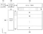
도 1은 본 발명의 실시예에 따른 표시장치를 보여 주는 블록도이다.
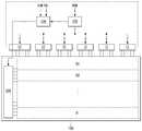
도 2는 게이트 구동부를 GIP 회로로 구현한 예를 보여 주는 도면이다.
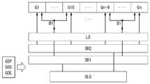
도 3 및 도 4는 게이트 구동부의 회로 구성을 보여 주는 도면이다.
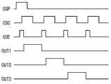
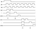
도 5는 라인 순차 구동 모드에서 게이트 구동부의 입출력 파형을 보여 주는 파형도이다.
도 6은 블록 구동 모드에서 게이트 구동부의 입출력 파형을 보여 주는 파형도이다.
도 7은 1 프레임 기간 내에서 라인 순차 구동 모드와 블록 구동 모드가 함께 적용된 예를 보여 주는 파형도이다.1 is a block diagram showing a display device according to an embodiment of the present invention.
2 is a diagram illustrating an example of a gate driver implemented by a GIP circuit.
3 and 4 are diagrams showing the circuit configuration of the gate driver.
5 is a waveform diagram showing an input / output waveform of the gate driver in the line-sequential driving mode.
6 is a waveform diagram showing an input / output waveform of the gate driver in the block driving mode.
FIG. 7 is a waveform diagram showing an example in which a line sequential drive mode and a block drive mode are applied together within one frame period.
본 발명의 표시장치는 액정표시장치(LCD), 유기 발광 다이오드 표시장치(OLED Display), 플라즈마 디스플레이 패널(Plasma Display Panel: PDP) 등 컬러 구현이 가능한 평판 표시장치로 구현될 수 있다.The display device of the present invention can be implemented as a flat panel display device capable of color display such as a liquid crystal display (LCD), an organic light emitting diode display (OLED) display, and a plasma display panel (PDP).
이하 첨부된 도면을 참조하여 본 발명에 따른 바람직한 실시예들을 상세히 설명한다. 명세서 전체에 걸쳐서 동일한 참조번호들은 실질적으로 동일한 구성요소들을 의미한다. 이하의 설명에서, 본 발명과 관련된 공지 기능 혹은 구성에 대한 구체적인 설명이 본 발명의 요지를 불필요하게 흐릴 수 있다고 판단되는 경우, 그 상세한 설명을 생략한다.DETAILED DESCRIPTION OF THE PREFERRED EMBODIMENTS Reference will now be made in detail to the preferred embodiments of the present invention, examples of which are illustrated in the accompanying drawings. Like reference numerals throughout the specification denote substantially identical components. In the following description, a detailed description of known functions and configurations incorporated herein will be omitted when it may make the subject matter of the present invention rather unclear.
도 1 내지 도 3을 참조하면, 본 발명의 표시장치는 픽셀 어레이가 형성된 표시패널(100)과, 표시패널(100)에 입력 영상의 데이터를 기입하기 위한 표시패널 구동회로를 구비한다.1 to 3, the display device of the present invention includes a
입력 영상은 표시패널(100)의 픽셀 어레이에 표시된다. 픽셀 어레이는 데이터라인들(S1~Sm)과 게이트라인들(G1~Gn)의 교차 구조에 의해 매트릭스 형태로 배열되는 픽셀들을 포함한다. 픽셀들 각각은 데이터 전압이 공급되는 픽셀 전극, 스위치 소자 및/또는 구동 소자로 동작하는 하나 이상의 TFT와, 하나 이상의 커패시터를 포함할 수 있다.The input image is displayed on the pixel array of the
표시패널 구동회로는 데이터 구동부(102), 게이트 구동부(104), 및 타이밍 콘트롤러(106)를 포함한다.The display panel drive circuit includes a
데이터 구동부(102)는 다수의 소스 드라이브 IC(도 2, 12)를 포함한다. 소스 드라이브 IC들(12)의 데이터 출력 채널들은 m(m은 양의 정수) 개의 데이터라인들(S1~Sm)에 연결된다. 소스 드라이브 IC들(12)은 타이밍 콘트롤러(106)로부터 입력 영상의 데이터를 입력 받는다. 소스 드라이브 IC들(12)은 타이밍 콘트롤러(106)의 제어 하에 입력 영상의 디지털 비디오 데이터를 정극성/부극성 감마보상전압으로 변환하여 정극성/부극성 데이터전압을 출력한다. 소스 드라이브 IC들(12)의 출력 전압은 데이터 라인들(S1~Sm)에 공급된다.The
소스 드라이드 IC들 각각은 타이밍 콘트롤러(106)의 제어 하에 픽셀들에 공급될 데이터 전압의 극성을 반전시켜 데이터 라인들(S1~Sm)로 출력한다.Each of the source driver ICs inverts the polarity of the data voltage to be supplied to the pixels under the control of the
게이트 구동부(104)는 타이밍 콘트롤러(106)의 제어 하에 n(n은 양의 정수)게이트 라인들(G1~Gn)에 게이트 펄스를 공급한다. 게이트 구동부(104)는 블록 구동 모드에서 게이트 펄스를 순차 블록 단위로 출력하고, 라인 순차 구동 모드에서 라인 단위로 순차 출력한다. 블록(B1~Bi)은 N(N은 2 이상 n/2 이하의 양의 정수) 개의 게이트 라인들을 포함한다. 라인은 하나의 게이트 라인을 의미한다. 예를 들어, 게이트 구동부(104)는 블록 구동 모드에서 제1 블록(B1)의 게이트 라인들로 게이트 펄스를 동시에 출력한 후에, 제2 블록(B2)의 게이트 라인들로 게이트 펄스를 동시에 출력한다. 게이트 구동부(104)는 라인 순차 구동 모드에서 게이트 펄스를 1 라인씩 게이트 라인들에 순차적으로 출력한다.The
타이밍 콘트롤러(106)는 입력 영상 데이터와 동기되는 타이밍 신호들을 호스트 시스템(110)으로부터 수신한다. 타이밍 콘트롤러(106)는 호스트 시스템(110)으로부터 수신된 입력 영상의 데이터를 데이터 구동부(102)로 전송한다. 타이밍 신호들은 수직 동기신호(Vsync), 수평 동기신호(Hsync), 데이터 인에이블 신호(DE), 메인 클럭(CLK) 등을 포함한다. 타이밍 콘트롤러(106)는 입력 영상의 픽셀 데이터와 함께 수신되는 타이밍 신호들(Vsync, Hsync, DE, CLK)을 바탕으로 데이터 구동부(102)와 게이트 구동부(104)의 동작 타이밍을 제어한다.The
호스트 시스템(110)은 TV(Television) 시스템, 셋톱박스, 네비게이션 시스템, DVD 플레이어, 블루레이 플레이어, 개인용 컴퓨터(PC), 홈 시어터 시스템, 폰 시스템(Phone system) 중 어느 하나일 수 있다.The
게이트 구동부(104)가 집적된 IC는 TAB(Tape Automated Bonding) 공정으로 표시패널(100)에 접착되어 게이트 라인들(G1~Gn)에 연결될 수 있다. 또한, 게이트 구동부(104)는 GIP(Gate In Panel) 공정으로 픽셀 어레이가 형성된 표시패널(100)의 기판 표면에 직접 형성될 수 있다.The IC in which the
도 2는 GIP 공정으로 표시패널에 직접 형성된 게이트 구동부(104)를 나타낸다. 게이트 구동부(104)는 게이트 타이밍 제어신호(GSP, GSC, GOE)에 응답하여 출력을 발생하는 제1 및 제2 시프트 레지스터(shift register)와, 제1 및 제2 시프트 레지스터를 선택하는 제어부를 포함한다. 제1 및 제2 시프트 레지스터와, 제어부의 기능은 도 3에 도시된 IC 내의 시프트 레지스터들 및 제어부와 실질적으로 동일하다. 도 2에서, 레벨 시프터(108)는 타이밍 콘트롤러로부터 게이트 구부(104)로 전달되는 게이트 타이밍 제어신호(GSP, GSC, GOE)의 전압 레벨을 게이트 하이 전압(VGH)과 게이트 로우 전압(VGL) 사이에서 스윙하는 전압으로 변환한다. 게이트 하이 전압(VGH)은 픽셀 어레이의 TFT를 턴-온시킬 수 있는 문턱 전압 이상의 전압이고, 게이트 로우 전압(VGL)은 TFT의 문턱 전압보다 낮은 전압이다.2 shows the
타이밍 콘트롤러(106)로부터 발생되는 게이트 타이밍 제어신호는 게이트 스타트 펄스(Gate Start Pulse, GSP), 게이트 시프트 클럭(Gate Shift Clock, GSC), 게이트 출력 인에이블신호(Gate Output Enable, GOE) 등을 포함한다. 게이트 스타트 펄스(GSP)는 첫 번째 게이트 펄스의 출력 타이밍을 제어한다. 게이트 시프트 클럭(GSC)은 게이트 펄스의 시프트 타이밍을 제어한다. 게이트 출력 인에이블신호(GOE)는 게이트 펄스들 각각의 출력 타이밍을 을 제어한다.The gate timing control signal generated from the
도 3 및 도 4는 TAB 공정으로 표시패널(100)에 접착되는 게이트 구동부의 IC 내부 구성을 보여 도면들이다.3 and 4 are views showing the internal structure of an IC of a gate driving unit adhered to the
도 3 및 도 4를 참조하면, 게이트 구동부(104)는 제어부(SLC), 제1 시프트 레지스터(SR1), 제2 시프트 레지스터(SR2), 레벨 쉬프터(62) 등을 포함한다.3 and 4, the
제어부(SLC)는 타이밍 콘트롤러(106)의 제어 하에 블록 구동 모드에서 게이트 시프트 클럭(GSC)을 제1 GSC 배선(41)을 통해 제1 시프트 레지스터(SR1)에 공급한다. 제어부(SLC)는 타이밍 콘트롤러(106)의 제어 하에 라인 순차 구동 모드에서 게이트 시프트 클럭(GSC)을 제2 GSC 배선(42)을 통해 제2 시프트 레지스터(SR2)에 공급한다. 제어부(SLC)는 타이밍 콘트롤러(106) 또는 데이터 구동부(108)에 내장될 수 있다.The control unit SLC supplies the gate shift clock GSC to the first shift register SR1 through the
제1 및 제2 시프트 레지스터(SR1, SR2)는 게이트 스타트 펄스(GSP)를 공통으로 수신하고, 게이트 스타트 펄스(GSC)를 제어부(SLC)를 통해 개별 수신한다. 따라서, 제1 및 제2 시프트 레지스터(SR1, SR2)는 제어부(SLC)의 선택에 따라 개별적으로 동작한다.The first and second shift registers SR1 and SR2 commonly receive the gate start pulse GSP and individually receive the gate start pulse GSC through the control section SLC. Therefore, the first and second shift registers SR1 and SR2 operate individually according to the selection of the control unit SLC.
제1 시프트 레지스터(SR1)는 종속적으로 접속된 다수의 D-플립 플롭(FF)을 포함한다. 제1 시프트 레지시터(SR1)는 게이트 스타트 펄스(GSP)를 게이트 시프트 클럭(GSC)에 따라 순차적으로 시프트시켜 1 블록 단위로 시프트되는 게이트 펄스를 출력한다.The first shift register SR1 includes a plurality of D-flip-flops (FFs) connected in a dependent manner. The first shift register SR1 sequentially shifts the gate start pulse GSP in accordance with the gate shift clock GSC and outputs a gate pulse shifted in units of one block.
제2 시프트 레지스터(SR2)는 종속적으로 접속된 다수의 D-플립 플롭(FF)을 포함한다. 제2 시프트 레지시터(SR2)는 게이트 스타트 펄스(GSP)를 게이트 시프트 클럭(GSC)에 따라 순차적으로 시프트시켜 1 라인 단위로 시프트되는 게이트 펄스를 출력한다.The second shift register SR2 includes a plurality of D-flip flops (FFs) connected in a dependent manner. The second shift register SR2 sequentially shifts the gate start pulse GSP in accordance with the gate shift clock GSC and outputs a gate pulse shifted by one line unit.
AND 게이트들(51, 54, 61, 64) 각각은 GOE 배선(44)을 통해 입력된 신호와 시프트 레지스터(SR1, SR2)의 출력(43)을 논리곱 연산하여 그 결과를 레벨 시프터레벨 시프터(52, 55, 62, 65)로 출력한다. 인버터(INV)는 게이트 출력 인에이블신호(GOE)를 반전시켜 GOE 배선(44)을 통해 AND 게이트들(51, 61, 54, 64)에 공급한다.Each of the AND
레벨 시프터(52, 55, 62, 65)는 AND 게이트(61)의 출력 전압을 변경한다. 레벨 시프터(52, 55, 62, 65)의 출력 전압은 버퍼(53)를 통해 OR 게이트(81, 82, 83, 84)에 공급된다.The level shifters 52, 55, 62 and 65 change the output voltage of the AND
이하에서, 10 개의 게이트 라인들이 하나의 블록에 속하는 예를 가정하여 설명하기로 한다. 도 4 내지 도 7에서 "OUT1~OUT10"은 제1 블록(B1)에 속한 게이트 라인들(G1~G10)에 공급되는 게이트 구동부(10)의 출력 전압이다. "OUT11~OUT20"은 제2 블록(B2)에 속한 게이트 라인들(G11~G20)에 공급되는 게이트 구동부(10)의 출력 전압이다.Hereinafter, it is assumed that ten gate lines belong to one block. 4 to 7, "OUT1 to OUT10" are the output voltages of the
제1 시프트 레지스터(SR1)의 제1 출력 전압은 제1 AND 게이트(51), 제1 레벨 시프터(52), 제1 버퍼(53), 및 제1 공통 배선(45)을 통해 OR 게이트(81, 83)에 공급된다. 제1 공통 배선(45)은 제1 내지 제10 게이트 라인들(G1~G10)에 연결된 OR 게이트들(81, 83)의 제1 입력 단자에 제1 시프트 레지스터(SR1)의 제1 출력 전압을 동시에 공급한다. 제2 시프트 레지스터(SR2)에서 순차적으로 출력되는 제1 내지 제10 출력 전압은 제2 AND 게이트(61), 제2 레벨 시프터(62), 제2 버퍼(63), 및 버퍼 출력 단자(46)를 통해 제2 OR 게이트(83)에 공급된다.The first output voltage of the first shift register SR1 is connected to the
OR 게이트(81, 83)는 제1 공통 배선(45)을 통해 입력된 제1 입력과 버퍼 출력 단자(46)를 통해 입력된 제2 입력을 논리합 연산하여 그 결과를 제1 블록(B1)에 속한 제1 내지 제10 게이트 라인들(G1~G10)로 출력한다. 제1 시프트 레지스터(SR1)는 블록 구동 모드에서 출력을 발생하고, 제2 시프트 레지스터(SR2)는 라인 순차 구동 모드에서 출력을 발생한다. 따라서, OR 게이트(81, 83)는 블록 구동 모드에서 제1 시프트 레지스터(SR1)의 제1 출력 전압을 제1 블록(B1)에 속한 제1 내지 제10 게이트 라인들(G1~G10)에 공급한다. 반면에, OR 게이트(81, 83)는 라인 순차 구동 모드에서 제2 시프트 레지스터(SR2)로부터 순차적으로 입력되는 출력 전압을 제1 내지 제10 게이트 라인들(G1~G10)에 공급한다.The OR
제1 시프트 레지스터(SR1)의 제2 출력 전압은 제3 AND 게이트(54), 제3 레벨 시프터(55), 제3 버퍼(56), 및 제2 공통 배선(47)을 통해 OR 게이트(82, 84)에 공급된다. 제2 공통 배선(47)은 제11 내지 제20 게이트 라인들(G11~G20)에 연결된 OR 게이트들(82, 84)의 제1 입력 단자에 제1 시프트 레지스터(SR1)의 제2 출력 전압을 동시에 공급한다. 제2 시프트 레지스터(SR2)에서 순차적으로 출력되는 제11 내지 제20 출력 전압은 제4 AND 게이트(64), 제4 레벨 시프터(65), 제4 버퍼(66), 및 버퍼 출력 단자(48)를 통해 제4 OR 게이트(84)에 공급된다.The second output voltage of the first shift register SR1 is connected to the
OR 게이트(82, 84)는 제2 공통 배선(47)을 통해 입력된 제1 입력과 버퍼 출력 단자(48)를 통해 입력된 제2 입력을 논리합 연산하여 그 결과를 제2 블록(B2)에 속한 제11 내지 제20 게이트 라인들(G11~G20)로 출력한다. 제1 시프트 레지스터(SR1)는 블록 구동 모드에서 출력을 발생하고, 제2 시프트 레지스터(SR2)는 라인 순차 구동 모드에서 출력을 발생한다. 따라서, OR 게이트(82, 84)는 블록 구동 모드에서 제1 시프트 레지스터(SR1)의 제2 출력 전압을 제2 블록(B2)에 속한 제11 내지 제20 게이트 라인들(G11~G20)에 공급한다. 반면에, OR 게이트(82, 84)는 라인 순차 구동 모드에서 제2 시프트 레지스터(SR2)로부터 순차적으로 입력되는 출력 전압을 제11 내지 제20 게이트 라인들(G11~G20)에 공급한다.The OR
한편, 레벨 시프터(LS)는 GIP 회로의 경우에, 도 2와 같이 게이트 구동부(104)의 입력 단에 배치된다.On the other hand, in the case of the GIP circuit, the level shifter LS is arranged at the input end of the
도 5는 라인 순차 구동 모드에서 게이트 구동부(104)의 입출력 파형을 보여 주는 파형도이다. 도 6은 블록 구동 모드에서 게이트 구동부(104)의 입출력 파형을 보여 주는 파형도이다. 도 7은 1 프레임 기간 내에서 라인 순차 구동 모드와 블록 구동 모드가 함께 적용된 예를 보여 주는 파형도이다.5 is a waveform diagram showing an input / output waveform of the
라인 순차 구동 모드는 데이터 전압에 동기되는 게이트 펄스를 게이트 라인들(G1~Gn)에 순차적으로 공급한다. 블록 구동 모드는 블록 단위로 게이트 펄스를 게이트 라인들에 순차적으로 공급한다. 예를 들어, 제1 내지 제10 게이트 라인들에 게이트 펄스가 동시에 출력된 후에, 제11 내지 제20 게이트 라인들에 게이트 펄스가 동시에 출력된다. 1 프레임 기간 동안 라인 순차 구동 모드와 블록 구동 모드가 함께 적용될 수 있다.The line sequential driving mode sequentially supplies gate pulses synchronized with the data voltages to the gate lines G1 to Gn. The block driving mode sequentially supplies gate pulses to the gate lines in block units. For example, after the gate pulses are output simultaneously to the first to tenth gate lines, gate pulses are simultaneously output to the eleventh to twentieth gate lines. The line sequential drive mode and the block drive mode can be applied together for one frame period.
라인 순차 구동 모드는 입력 영상의 데이터가 픽셀들에 기입되는 상황에서 이용될 수 있다. 블록 구동 모드는 블록 단위로 픽셀들을 방전, 초기화하거나 3D 모드에서 픽셀들에 블랙 데이터를 기입하거나 TFT 특성의 경시 변화를 센싱하는데 적용될 수 있다. 또한, 블록 구동 모드는 다수의 라인들에 배치된 픽셀들에 블랙 데이터(black data)를 기입하여 BDI(Black Data Insertion) 효과를 얻거나 3D 영상을 표시할 때 좌안 영상과 우안 영상 사이에서 블랙 데이터를 삽입할 때 적용될 수 있다. 도 7과 같이, 1 프레임 기간 내에서 라인 순차 모드(71)와 블록 구동 모드(72)가 함께 적용될 수 있다.The line sequential drive mode can be used in a situation where data of an input image is written to pixels. The block drive mode can be applied to discharge or initialize pixels on a block-by-block basis, to write black data to pixels in 3D mode, or to sense changes in TFT characteristics over time. In the block driving mode, black data is written to pixels arranged in a plurality of lines to obtain a BDI (Black Data Insertion) effect, or when a 3D image is displayed, black data Can be applied. As shown in FIG. 7, the line
이상 설명한 내용을 통해 당업자라면 본 발명의 기술사상을 일탈하지 아니하는 범위에서 다양한 변경 및 수정이 가능함을 알 수 있을 것이다. 따라서, 본 발명의 기술적 범위는 명세서의 상세한 설명에 기재된 내용으로 한정되는 것이 아니라 특허 청구의 범위에 의해 정하여져야만 할 것이다.
It will be apparent to those skilled in the art that various modifications and variations can be made in the present invention without departing from the spirit or scope of the invention. Therefore, the technical scope of the present invention should not be limited to the contents described in the detailed description of the specification, but should be defined by the claims.
100 : 표시패널102 : 데이터 구동부
104 : 게이트 구동부106 : 타이밍 콘트롤러
110 : 호스트 시스템100: display panel 102: data driver
104: Gate driver 106: Timing controller
110: host system
Claims (4)
Translated fromKorean게이트 스타트 펄스를 게이트 시프트 클럭에 따라 순차적으로 시프트시켜 다수의 게이트 라인들이 속한 블록 단위로 시프트되는 게이트 펄스를 출력하는 제1 시프트 레지스터;
상기 게이트 스타트 펄스를 상기 게이트 시프트 클럭에 따라 게이트 라인 단위로 시프트되는 게이트 펄스를 출력하는 제2 시프트 레지스터; 및
상기 제1 및 제2 시프트 레지스터들 중에서 어느 하나에 상기 게이트 시프트 클럭을 공급하는 제어부를 포함하는 것을 특징으로 하는 표시장치.A pixel array including pixels arranged in a matrix form by a cross structure of data lines and gate lines;
A first shift register for sequentially shifting a gate start pulse according to a gate shift clock to output a gate pulse shifted in a block unit to which a plurality of gate lines belong;
A second shift register for outputting the gate start pulse as a gate pulse shifted on a gate-line-by-gate basis in accordance with the gate shift clock; And
And a controller for supplying the gate shift clock to any one of the first and second shift registers.
상기 제1 시프트 레지스터의 제1 출력 전압은 제1 공통 배선을 통해 제1 블록에 속한 다수의 게이트 라인들에 연결된 제1 블록의 OR 게이트들에 공급되고,
상기 제2 시프트 레지스터에서 순차적으로 출력되는 출력 전압은 상기 제1 블록의 OR 게이트에 공급되고,
상기 제2 시프트 레지스터의 제2 출력 전압은 제2 공통 배선을 통해 제2 블록에 속한 다수의 게이트 라인들에 연결된 제2 블록의 OR 게이트들에 공급되고,
상기 제2 시프트 레지스터에서 순차적으로 출력되는 출력 전압은 상기 제2 블록의 OR 게이트에 공급되는 것을 특징으로 하는 표시장치.The method according to claim 1,
The first output voltage of the first shift register is supplied to the OR gates of the first block connected to the plurality of gate lines belonging to the first block through the first common wiring,
An output voltage sequentially output from the second shift register is supplied to the OR gate of the first block,
The second output voltage of the second shift register is supplied to the OR gates of the second block connected to the plurality of gate lines belonging to the second block via the second common wiring,
And an output voltage sequentially output from the second shift register is supplied to the OR gate of the second block.
상기 시프트 레지스터들과 상기 OR 게이트들 사이에 AND 게이트, 레벨 시프터, 및 버퍼를 포함하는 것을 특징으로 하는 표시장치.The method according to claim 1,
And an AND gate, a level shifter, and a buffer between the shift registers and the OR gates.
상기 제어부는
라인 순차 구동 모드에서 상기 제1 시프트 레지스터에 상기 게이트 시프트 클럭을 공급하여 데이터 전압에 동기되는 게이트 펄스를 상기 게이트 라인들에 순차적으로 공급하고,
블록 구동 모드에서 상기 제2 시프트 레지스터에 상기 게이트 시프트 클럭을 공급하여 블록 단위로 게이트 펄스를 게이트 라인들에 순차적으로 공급하는 표시장치.
The method according to claim 1,
The control unit
The gate shift clock is supplied to the first shift register in a line sequential driving mode to sequentially supply a gate pulse synchronized with a data voltage to the gate lines,
And supplies the gate shift clock to the second shift register in a block drive mode to sequentially supply gate pulses to the gate lines on a block-by-block basis.
Priority Applications (3)
| Application Number | Priority Date | Filing Date | Title |
|---|---|---|---|
| KR1020140123780AKR101661026B1 (en) | 2014-09-17 | 2014-09-17 | Display device |
| CN201510587311.7ACN105427783B (en) | 2014-09-17 | 2015-09-15 | Gate driving circuit and the display device for using the gate driving circuit |
| US14/857,411US9941018B2 (en) | 2014-09-17 | 2015-09-17 | Gate driving circuit and display device using the same |
Applications Claiming Priority (1)
| Application Number | Priority Date | Filing Date | Title |
|---|---|---|---|
| KR1020140123780AKR101661026B1 (en) | 2014-09-17 | 2014-09-17 | Display device |
Publications (2)
| Publication Number | Publication Date |
|---|---|
| KR20160033351Atrue KR20160033351A (en) | 2016-03-28 |
| KR101661026B1 KR101661026B1 (en) | 2016-09-29 |
Family
ID=55455326
Family Applications (1)
| Application Number | Title | Priority Date | Filing Date |
|---|---|---|---|
| KR1020140123780AActiveKR101661026B1 (en) | 2014-09-17 | 2014-09-17 | Display device |
Country Status (3)
| Country | Link |
|---|---|
| US (1) | US9941018B2 (en) |
| KR (1) | KR101661026B1 (en) |
| CN (1) | CN105427783B (en) |
Cited By (3)
| Publication number | Priority date | Publication date | Assignee | Title |
|---|---|---|---|---|
| KR20180127896A (en)* | 2017-05-22 | 2018-11-30 | 엘지디스플레이 주식회사 | Active Matrix Display Device |
| KR20200079579A (en)* | 2018-12-26 | 2020-07-06 | 주식회사 실리콘웍스 | Gate driving apparatus and display device |
| KR20210045034A (en)* | 2019-10-16 | 2021-04-26 | 엘지디스플레이 주식회사 | Display device, display panel, and gate driving circuit |
Families Citing this family (7)
| Publication number | Priority date | Publication date | Assignee | Title |
|---|---|---|---|---|
| KR102227481B1 (en)* | 2014-10-24 | 2021-03-15 | 삼성디스플레이 주식회사 | Display apparatus |
| US10891903B2 (en)* | 2017-12-18 | 2021-01-12 | Lg Display Co., Ltd. | Gate-in-panel gate driver and organic light emitting display device having the same |
| KR102459026B1 (en)* | 2018-05-21 | 2022-10-26 | 엘지디스플레이 주식회사 | Display device and method for driving the same |
| KR102653683B1 (en)* | 2018-09-12 | 2024-04-01 | 엘지디스플레이 주식회사 | Organic light emitting display apparatus |
| JP7463074B2 (en)* | 2019-10-17 | 2024-04-08 | エルジー ディスプレイ カンパニー リミテッド | Display control device, display device, and display control method |
| KR102676669B1 (en) | 2019-10-23 | 2024-06-21 | 삼성디스플레이 주식회사 | Display device and method of driving the same |
| CN113035111B (en)* | 2021-03-25 | 2022-01-14 | 惠科股份有限公司 | Gate drive circuit, drive device and display device |
Citations (4)
| Publication number | Priority date | Publication date | Assignee | Title |
|---|---|---|---|---|
| KR20030039972A (en)* | 2001-11-15 | 2003-05-22 | 삼성전자주식회사 | On-glass single chip liquid crystal display device |
| KR20100071387A (en)* | 2008-12-19 | 2010-06-29 | 엘지디스플레이 주식회사 | Gate driver |
| KR20100128019A (en)* | 2009-05-27 | 2010-12-07 | 엘지디스플레이 주식회사 | Image display device and its driving method |
| KR20120044784A (en)* | 2010-10-28 | 2012-05-08 | 삼성모바일디스플레이주식회사 | Driver, display device comprising the same |
Family Cites Families (8)
| Publication number | Priority date | Publication date | Assignee | Title |
|---|---|---|---|---|
| US5533187A (en)* | 1993-10-29 | 1996-07-02 | Sun Microsystems, Inc | Multiple block mode operations in a frame buffer system designed for windowing operations |
| JP3743504B2 (en)* | 2001-05-24 | 2006-02-08 | セイコーエプソン株式会社 | Scan driving circuit, display device, electro-optical device, and scan driving method |
| JP4551712B2 (en)* | 2004-08-06 | 2010-09-29 | 東芝モバイルディスプレイ株式会社 | Gate line drive circuit |
| JP4633434B2 (en)* | 2004-10-18 | 2011-02-16 | シャープ株式会社 | Semiconductor device and manufacturing method thereof |
| KR101127854B1 (en)* | 2005-09-27 | 2012-03-21 | 엘지디스플레이 주식회사 | Apparatus driving for gate and image display using the same |
| KR101073226B1 (en)* | 2010-03-17 | 2011-10-12 | 삼성모바일디스플레이주식회사 | Organic Light Emitting Display Device |
| CN102237055A (en)* | 2010-05-05 | 2011-11-09 | 联咏科技股份有限公司 | Gate driver for liquid crystal display (LCD) and driving method |
| KR101097353B1 (en)* | 2010-05-07 | 2011-12-23 | 삼성모바일디스플레이주식회사 | A gate driving circuit and a organic electroluminescent display apparatus using the same |
- 2014
- 2014-09-17KRKR1020140123780Apatent/KR101661026B1/enactiveActive
- 2015
- 2015-09-15CNCN201510587311.7Apatent/CN105427783B/enactiveActive
- 2015-09-17USUS14/857,411patent/US9941018B2/enactiveActive
Patent Citations (4)
| Publication number | Priority date | Publication date | Assignee | Title |
|---|---|---|---|---|
| KR20030039972A (en)* | 2001-11-15 | 2003-05-22 | 삼성전자주식회사 | On-glass single chip liquid crystal display device |
| KR20100071387A (en)* | 2008-12-19 | 2010-06-29 | 엘지디스플레이 주식회사 | Gate driver |
| KR20100128019A (en)* | 2009-05-27 | 2010-12-07 | 엘지디스플레이 주식회사 | Image display device and its driving method |
| KR20120044784A (en)* | 2010-10-28 | 2012-05-08 | 삼성모바일디스플레이주식회사 | Driver, display device comprising the same |
Cited By (3)
| Publication number | Priority date | Publication date | Assignee | Title |
|---|---|---|---|---|
| KR20180127896A (en)* | 2017-05-22 | 2018-11-30 | 엘지디스플레이 주식회사 | Active Matrix Display Device |
| KR20200079579A (en)* | 2018-12-26 | 2020-07-06 | 주식회사 실리콘웍스 | Gate driving apparatus and display device |
| KR20210045034A (en)* | 2019-10-16 | 2021-04-26 | 엘지디스플레이 주식회사 | Display device, display panel, and gate driving circuit |
Also Published As
| Publication number | Publication date |
|---|---|
| CN105427783A (en) | 2016-03-23 |
| US9941018B2 (en) | 2018-04-10 |
| KR101661026B1 (en) | 2016-09-29 |
| US20160078834A1 (en) | 2016-03-17 |
| CN105427783B (en) | 2018-08-31 |
Similar Documents
| Publication | Publication Date | Title |
|---|---|---|
| KR101661026B1 (en) | Display device | |
| CN109961732B (en) | Display device | |
| KR102169169B1 (en) | Display device and method for driving the same | |
| US20160070147A1 (en) | Liquid crystal display device | |
| KR102426106B1 (en) | Stage circuit and scan driver using the same | |
| KR102281753B1 (en) | Stage circuit and scan driver using the same | |
| KR102279280B1 (en) | Display Device and Driving Method for the Same | |
| KR20170079997A (en) | Gate driver and display device including the same | |
| KR102328638B1 (en) | Scan driver | |
| CN106097950A (en) | Display device | |
| JP7114875B2 (en) | ELECTRO-OPTICAL DEVICE, ELECTRO-OPTICAL DEVICE CONTROL METHOD, AND ELECTRONIC DEVICE | |
| KR102452523B1 (en) | Scan driver | |
| KR102279494B1 (en) | Liquid Crystal Display | |
| KR102312287B1 (en) | Scan driver and display device using the same | |
| US10497328B2 (en) | Display panel driving apparatus, method of driving display panel using the same, and display apparatus having the same | |
| CN102376284B (en) | Electro-optical device and electronic equipment | |
| KR20160044173A (en) | Display Panel With Narrow Bezel And Display Device Including The Same | |
| KR102364096B1 (en) | Display Device | |
| KR102148489B1 (en) | Power supplying apparatus for display device | |
| KR101989931B1 (en) | Liquid crystal display and undershoot generation circuit thereof | |
| US10304406B2 (en) | Display apparatus with reduced flash noise, and a method of driving the display apparatus | |
| KR102283377B1 (en) | Display device and gate driving circuit thereof | |
| KR102458522B1 (en) | Gate Driving Circuit for Display Device and Display Device having the same | |
| KR20170039807A (en) | Scan driver and driving method thereof | |
| KR20160077254A (en) | A crystal dispplay device |
Legal Events
| Date | Code | Title | Description |
|---|---|---|---|
| A201 | Request for examination | ||
| PA0109 | Patent application | St.27 status event code:A-0-1-A10-A12-nap-PA0109 | |
| PA0201 | Request for examination | St.27 status event code:A-1-2-D10-D11-exm-PA0201 | |
| D13-X000 | Search requested | St.27 status event code:A-1-2-D10-D13-srh-X000 | |
| D14-X000 | Search report completed | St.27 status event code:A-1-2-D10-D14-srh-X000 | |
| E902 | Notification of reason for refusal | ||
| PE0902 | Notice of grounds for rejection | St.27 status event code:A-1-2-D10-D21-exm-PE0902 | |
| P11-X000 | Amendment of application requested | St.27 status event code:A-2-2-P10-P11-nap-X000 | |
| P13-X000 | Application amended | St.27 status event code:A-2-2-P10-P13-nap-X000 | |
| PG1501 | Laying open of application | St.27 status event code:A-1-1-Q10-Q12-nap-PG1501 | |
| E701 | Decision to grant or registration of patent right | ||
| PE0701 | Decision of registration | St.27 status event code:A-1-2-D10-D22-exm-PE0701 | |
| GRNT | Written decision to grant | ||
| PR0701 | Registration of establishment | St.27 status event code:A-2-4-F10-F11-exm-PR0701 | |
| PR1002 | Payment of registration fee | St.27 status event code:A-2-2-U10-U11-oth-PR1002 Fee payment year number:1 | |
| PG1601 | Publication of registration | St.27 status event code:A-4-4-Q10-Q13-nap-PG1601 | |
| PR1001 | Payment of annual fee | St.27 status event code:A-4-4-U10-U11-oth-PR1001 Fee payment year number:4 | |
| PR1001 | Payment of annual fee | St.27 status event code:A-4-4-U10-U11-oth-PR1001 Fee payment year number:5 | |
| PR1001 | Payment of annual fee | St.27 status event code:A-4-4-U10-U11-oth-PR1001 Fee payment year number:6 | |
| PR1001 | Payment of annual fee | St.27 status event code:A-4-4-U10-U11-oth-PR1001 Fee payment year number:7 | |
| PR1001 | Payment of annual fee | St.27 status event code:A-4-4-U10-U11-oth-PR1001 Fee payment year number:8 | |
| PR1001 | Payment of annual fee | St.27 status event code:A-4-4-U10-U11-oth-PR1001 Fee payment year number:9 | |
| PR1001 | Payment of annual fee | St.27 status event code:A-4-4-U10-U11-oth-PR1001 Fee payment year number:10 |