KR20160029595A - Semiconductor package - Google Patents
Semiconductor packageDownload PDFInfo
- Publication number
- KR20160029595A KR20160029595AKR1020140119369AKR20140119369AKR20160029595AKR 20160029595 AKR20160029595 AKR 20160029595AKR 1020140119369 AKR1020140119369 AKR 1020140119369AKR 20140119369 AKR20140119369 AKR 20140119369AKR 20160029595 AKR20160029595 AKR 20160029595A
- Authority
- KR
- South Korea
- Prior art keywords
- semiconductor chip
- package substrate
- semiconductor
- spacer
- package
- Prior art date
- Legal status (The legal status is an assumption and is not a legal conclusion. Google has not performed a legal analysis and makes no representation as to the accuracy of the status listed.)
- Granted
Links
Images


Classifications
- H—ELECTRICITY
- H01—ELECTRIC ELEMENTS
- H01L—SEMICONDUCTOR DEVICES NOT COVERED BY CLASS H10
- H01L23/00—Details of semiconductor or other solid state devices
- H01L23/58—Structural electrical arrangements for semiconductor devices not otherwise provided for, e.g. in combination with batteries
- H—ELECTRICITY
- H01—ELECTRIC ELEMENTS
- H01L—SEMICONDUCTOR DEVICES NOT COVERED BY CLASS H10
- H01L23/00—Details of semiconductor or other solid state devices
- H01L23/52—Arrangements for conducting electric current within the device in operation from one component to another, i.e. interconnections, e.g. wires, lead frames
- H01L23/538—Arrangements for conducting electric current within the device in operation from one component to another, i.e. interconnections, e.g. wires, lead frames the interconnection structure between a plurality of semiconductor chips being formed on, or in, insulating substrates
- H01L23/5384—Conductive vias through the substrate with or without pins, e.g. buried coaxial conductors
- H—ELECTRICITY
- H01—ELECTRIC ELEMENTS
- H01L—SEMICONDUCTOR DEVICES NOT COVERED BY CLASS H10
- H01L23/00—Details of semiconductor or other solid state devices
- H01L23/52—Arrangements for conducting electric current within the device in operation from one component to another, i.e. interconnections, e.g. wires, lead frames
- H01L23/522—Arrangements for conducting electric current within the device in operation from one component to another, i.e. interconnections, e.g. wires, lead frames including external interconnections consisting of a multilayer structure of conductive and insulating layers inseparably formed on the semiconductor body
- H01L23/5226—Via connections in a multilevel interconnection structure
- H—ELECTRICITY
- H01—ELECTRIC ELEMENTS
- H01L—SEMICONDUCTOR DEVICES NOT COVERED BY CLASS H10
- H01L23/00—Details of semiconductor or other solid state devices
- H01L23/52—Arrangements for conducting electric current within the device in operation from one component to another, i.e. interconnections, e.g. wires, lead frames
- H01L23/522—Arrangements for conducting electric current within the device in operation from one component to another, i.e. interconnections, e.g. wires, lead frames including external interconnections consisting of a multilayer structure of conductive and insulating layers inseparably formed on the semiconductor body
- H01L23/528—Layout of the interconnection structure
- H01L23/5286—Arrangements of power or ground buses
- H—ELECTRICITY
- H01—ELECTRIC ELEMENTS
- H01L—SEMICONDUCTOR DEVICES NOT COVERED BY CLASS H10
- H01L23/00—Details of semiconductor or other solid state devices
- H01L23/552—Protection against radiation, e.g. light or electromagnetic waves
- H—ELECTRICITY
- H01—ELECTRIC ELEMENTS
- H01L—SEMICONDUCTOR DEVICES NOT COVERED BY CLASS H10
- H01L25/00—Assemblies consisting of a plurality of semiconductor or other solid state devices
- H01L25/03—Assemblies consisting of a plurality of semiconductor or other solid state devices all the devices being of a type provided for in a single subclass of subclasses H10B, H10D, H10F, H10H, H10K or H10N, e.g. assemblies of rectifier diodes
- H01L25/04—Assemblies consisting of a plurality of semiconductor or other solid state devices all the devices being of a type provided for in a single subclass of subclasses H10B, H10D, H10F, H10H, H10K or H10N, e.g. assemblies of rectifier diodes the devices not having separate containers
- H01L25/065—Assemblies consisting of a plurality of semiconductor or other solid state devices all the devices being of a type provided for in a single subclass of subclasses H10B, H10D, H10F, H10H, H10K or H10N, e.g. assemblies of rectifier diodes the devices not having separate containers the devices being of a type provided for in group H10D89/00
- H01L25/0657—Stacked arrangements of devices
- H—ELECTRICITY
- H01—ELECTRIC ELEMENTS
- H01L—SEMICONDUCTOR DEVICES NOT COVERED BY CLASS H10
- H01L2224/00—Indexing scheme for arrangements for connecting or disconnecting semiconductor or solid-state bodies and methods related thereto as covered by H01L24/00
- H01L2224/01—Means for bonding being attached to, or being formed on, the surface to be connected, e.g. chip-to-package, die-attach, "first-level" interconnects; Manufacturing methods related thereto
- H01L2224/26—Layer connectors, e.g. plate connectors, solder or adhesive layers; Manufacturing methods related thereto
- H01L2224/31—Structure, shape, material or disposition of the layer connectors after the connecting process
- H01L2224/32—Structure, shape, material or disposition of the layer connectors after the connecting process of an individual layer connector
- H01L2224/321—Disposition
- H01L2224/32135—Disposition the layer connector connecting between different semiconductor or solid-state bodies, i.e. chip-to-chip
- H01L2224/32145—Disposition the layer connector connecting between different semiconductor or solid-state bodies, i.e. chip-to-chip the bodies being stacked
- H—ELECTRICITY
- H01—ELECTRIC ELEMENTS
- H01L—SEMICONDUCTOR DEVICES NOT COVERED BY CLASS H10
- H01L2224/00—Indexing scheme for arrangements for connecting or disconnecting semiconductor or solid-state bodies and methods related thereto as covered by H01L24/00
- H01L2224/01—Means for bonding being attached to, or being formed on, the surface to be connected, e.g. chip-to-package, die-attach, "first-level" interconnects; Manufacturing methods related thereto
- H01L2224/26—Layer connectors, e.g. plate connectors, solder or adhesive layers; Manufacturing methods related thereto
- H01L2224/31—Structure, shape, material or disposition of the layer connectors after the connecting process
- H01L2224/32—Structure, shape, material or disposition of the layer connectors after the connecting process of an individual layer connector
- H01L2224/321—Disposition
- H01L2224/32151—Disposition the layer connector connecting between a semiconductor or solid-state body and an item not being a semiconductor or solid-state body, e.g. chip-to-substrate, chip-to-passive
- H01L2224/32221—Disposition the layer connector connecting between a semiconductor or solid-state body and an item not being a semiconductor or solid-state body, e.g. chip-to-substrate, chip-to-passive the body and the item being stacked
- H01L2224/32225—Disposition the layer connector connecting between a semiconductor or solid-state body and an item not being a semiconductor or solid-state body, e.g. chip-to-substrate, chip-to-passive the body and the item being stacked the item being non-metallic, e.g. insulating substrate with or without metallisation
- H—ELECTRICITY
- H01—ELECTRIC ELEMENTS
- H01L—SEMICONDUCTOR DEVICES NOT COVERED BY CLASS H10
- H01L2224/00—Indexing scheme for arrangements for connecting or disconnecting semiconductor or solid-state bodies and methods related thereto as covered by H01L24/00
- H01L2224/01—Means for bonding being attached to, or being formed on, the surface to be connected, e.g. chip-to-package, die-attach, "first-level" interconnects; Manufacturing methods related thereto
- H01L2224/42—Wire connectors; Manufacturing methods related thereto
- H01L2224/47—Structure, shape, material or disposition of the wire connectors after the connecting process
- H01L2224/48—Structure, shape, material or disposition of the wire connectors after the connecting process of an individual wire connector
- H01L2224/4805—Shape
- H01L2224/4809—Loop shape
- H01L2224/48091—Arched
- H—ELECTRICITY
- H01—ELECTRIC ELEMENTS
- H01L—SEMICONDUCTOR DEVICES NOT COVERED BY CLASS H10
- H01L2224/00—Indexing scheme for arrangements for connecting or disconnecting semiconductor or solid-state bodies and methods related thereto as covered by H01L24/00
- H01L2224/01—Means for bonding being attached to, or being formed on, the surface to be connected, e.g. chip-to-package, die-attach, "first-level" interconnects; Manufacturing methods related thereto
- H01L2224/42—Wire connectors; Manufacturing methods related thereto
- H01L2224/47—Structure, shape, material or disposition of the wire connectors after the connecting process
- H01L2224/48—Structure, shape, material or disposition of the wire connectors after the connecting process of an individual wire connector
- H01L2224/481—Disposition
- H01L2224/48135—Connecting between different semiconductor or solid-state bodies, i.e. chip-to-chip
- H01L2224/48145—Connecting between different semiconductor or solid-state bodies, i.e. chip-to-chip the bodies being stacked
- H01L2224/48147—Connecting between different semiconductor or solid-state bodies, i.e. chip-to-chip the bodies being stacked with an intermediate bond, e.g. continuous wire daisy chain
- H—ELECTRICITY
- H01—ELECTRIC ELEMENTS
- H01L—SEMICONDUCTOR DEVICES NOT COVERED BY CLASS H10
- H01L2224/00—Indexing scheme for arrangements for connecting or disconnecting semiconductor or solid-state bodies and methods related thereto as covered by H01L24/00
- H01L2224/73—Means for bonding being of different types provided for in two or more of groups H01L2224/10, H01L2224/18, H01L2224/26, H01L2224/34, H01L2224/42, H01L2224/50, H01L2224/63, H01L2224/71
- H01L2224/732—Location after the connecting process
- H01L2224/73251—Location after the connecting process on different surfaces
- H01L2224/73265—Layer and wire connectors
- H—ELECTRICITY
- H01—ELECTRIC ELEMENTS
- H01L—SEMICONDUCTOR DEVICES NOT COVERED BY CLASS H10
- H01L2224/00—Indexing scheme for arrangements for connecting or disconnecting semiconductor or solid-state bodies and methods related thereto as covered by H01L24/00
- H01L2224/91—Methods for connecting semiconductor or solid state bodies including different methods provided for in two or more of groups H01L2224/80 - H01L2224/90
- H01L2224/92—Specific sequence of method steps
- H01L2224/922—Connecting different surfaces of the semiconductor or solid-state body with connectors of different types
- H01L2224/9222—Sequential connecting processes
- H01L2224/92242—Sequential connecting processes the first connecting process involving a layer connector
- H01L2224/92247—Sequential connecting processes the first connecting process involving a layer connector the second connecting process involving a wire connector
- H—ELECTRICITY
- H01—ELECTRIC ELEMENTS
- H01L—SEMICONDUCTOR DEVICES NOT COVERED BY CLASS H10
- H01L23/00—Details of semiconductor or other solid state devices
- H01L23/28—Encapsulations, e.g. encapsulating layers, coatings, e.g. for protection
- H01L23/31—Encapsulations, e.g. encapsulating layers, coatings, e.g. for protection characterised by the arrangement or shape
- H01L23/3107—Encapsulations, e.g. encapsulating layers, coatings, e.g. for protection characterised by the arrangement or shape the device being completely enclosed
- H01L23/3121—Encapsulations, e.g. encapsulating layers, coatings, e.g. for protection characterised by the arrangement or shape the device being completely enclosed a substrate forming part of the encapsulation
- H01L23/3128—Encapsulations, e.g. encapsulating layers, coatings, e.g. for protection characterised by the arrangement or shape the device being completely enclosed a substrate forming part of the encapsulation the substrate having spherical bumps for external connection
- H—ELECTRICITY
- H01—ELECTRIC ELEMENTS
- H01L—SEMICONDUCTOR DEVICES NOT COVERED BY CLASS H10
- H01L23/00—Details of semiconductor or other solid state devices
- H01L23/48—Arrangements for conducting electric current to or from the solid state body in operation, e.g. leads, terminal arrangements ; Selection of materials therefor
- H01L23/488—Arrangements for conducting electric current to or from the solid state body in operation, e.g. leads, terminal arrangements ; Selection of materials therefor consisting of soldered or bonded constructions
- H01L23/498—Leads, i.e. metallisations or lead-frames on insulating substrates, e.g. chip carriers
- H01L23/49811—Additional leads joined to the metallisation on the insulating substrate, e.g. pins, bumps, wires, flat leads
- H01L23/49816—Spherical bumps on the substrate for external connection, e.g. ball grid arrays [BGA]
- H—ELECTRICITY
- H01—ELECTRIC ELEMENTS
- H01L—SEMICONDUCTOR DEVICES NOT COVERED BY CLASS H10
- H01L2924/00—Indexing scheme for arrangements or methods for connecting or disconnecting semiconductor or solid-state bodies as covered by H01L24/00
- H01L2924/15—Details of package parts other than the semiconductor or other solid state devices to be connected
- H01L2924/151—Die mounting substrate
- H01L2924/153—Connection portion
- H01L2924/1531—Connection portion the connection portion being formed only on the surface of the substrate opposite to the die mounting surface
- H01L2924/15311—Connection portion the connection portion being formed only on the surface of the substrate opposite to the die mounting surface being a ball array, e.g. BGA
- H—ELECTRICITY
- H01—ELECTRIC ELEMENTS
- H01L—SEMICONDUCTOR DEVICES NOT COVERED BY CLASS H10
- H01L2924/00—Indexing scheme for arrangements or methods for connecting or disconnecting semiconductor or solid-state bodies as covered by H01L24/00
- H01L2924/15—Details of package parts other than the semiconductor or other solid state devices to be connected
- H01L2924/181—Encapsulation
- H—ELECTRICITY
- H01—ELECTRIC ELEMENTS
- H01L—SEMICONDUCTOR DEVICES NOT COVERED BY CLASS H10
- H01L2924/00—Indexing scheme for arrangements or methods for connecting or disconnecting semiconductor or solid-state bodies as covered by H01L24/00
- H01L2924/30—Technical effects
- H01L2924/301—Electrical effects
- H01L2924/3025—Electromagnetic shielding
Landscapes
- Physics & Mathematics (AREA)
- Engineering & Computer Science (AREA)
- Microelectronics & Electronic Packaging (AREA)
- Power Engineering (AREA)
- Condensed Matter Physics & Semiconductors (AREA)
- General Physics & Mathematics (AREA)
- Computer Hardware Design (AREA)
- Health & Medical Sciences (AREA)
- Electromagnetism (AREA)
- Toxicology (AREA)
- Geometry (AREA)
- Structures Or Materials For Encapsulating Or Coating Semiconductor Devices Or Solid State Devices (AREA)
Abstract
Translated fromKoreanDescription
Translated fromKorean본 발명은 반도체 패키지에 관한 것으로, 더욱 상세하게는 패키지에 포함된 반도체 칩 등을 외부 환경으로부터 보호함과 동시에 전자파를 차폐할 수 있는 전자파 차폐 부재를 구비하는 반도체 패키지에 관한 것이다.BACKGROUND OF THE
최근 전자제품 시장은 휴대용 장치의 수요가 급격하게 증가하고 있으며, 이로 인하여 이들 제품에 실장되는 전자 부품들의 소형화 및 경량화가 지속적으로 요구되고 있다. 이러한 전자 부품들의 소형화 및 경량화를 실현하기 위해서는 실장 부품의 개별 사이즈를 감소시키는 기술뿐만 아니라, 다수의 개별 소자들을 하나의 패키지로 집적하는 반도체 패키지 기술이 요구된다. 특히, 고주파 신호를 취급하는 반도체 패키지는 소형화뿐만 아니라 전자파 간섭 또는 전자파 내성 특성을 우수하게 구현하기 위해 다양한 전자파 차폐 구조를 구비할 것이 요구되고 있다.Recently, demand for portable devices has been rapidly increasing in the electronic products market, and there is a continuing demand for miniaturization and weight reduction of electronic components mounted on these products. In order to realize miniaturization and weight reduction of such electronic parts, there is a need for a technique for reducing individual sizes of mounting parts as well as a semiconductor package technology for integrating a plurality of individual elements into one package. In particular, semiconductor packages for handling high frequency signals are required to have various electromagnetic wave shielding structures in order to realize miniaturization as well as electromagnetic wave interference or electromagnetic wave immunity characteristics.
본 발명의 기술적 사상이 해결하고자 하는 과제는 반도체 패키지를 경박단소화 하면서 동시에 전자파 간섭 특성이 우수한 전자파 차폐 구조를 갖는 반도체 패키지를 제공하는 것을 목적으로 한다.SUMMARY OF THE INVENTION It is an object of the present invention to provide a semiconductor package having an electromagnetic wave shielding structure that is thin and light in weight and has excellent electromagnetic wave interference characteristics.
본 발명의 기술적 사상에 의한 일 실시예에 따른 반도체 패키지는, 접지 패드를 포함하는 패키지 기판; 상기 패키지 기판 상에 배치되는 도전성 스페이서 및 제1 반도체 칩; 상기 도전성 스페이서 및 제1 반도체 칩 상에 걸쳐서 적층되는 제2 반도체 칩; 상기 패키지 기판, 제1 반도체 칩 및 제2 반도체 칩을 덮고 상기 도전성 스페이서의 일부를 노출시키는 몰딩 부재; 및 상기 몰딩 부재의 표면을 덮는 전자파 차폐 부재를 포함하는 것을 특징으로 한다.According to an aspect of the present invention, there is provided a semiconductor package including: a package substrate including a ground pad; A conductive spacer and a first semiconductor chip disposed on the package substrate; A second semiconductor chip stacked over the conductive spacer and the first semiconductor chip; A molding member covering the package substrate, the first semiconductor chip and the second semiconductor chip and exposing a part of the conductive spacer; And an electromagnetic wave shielding member covering the surface of the molding member.
예시적인 실시예들에서, 상기 몰딩 부재에서 노출되는 도전성 스페이서의 일부에 상기 전자파 차폐 부재가 전기적으로 연결되는 것을 특징으로 한다.In exemplary embodiments, the electromagnetic shielding member is electrically connected to a part of the conductive spacer exposed in the molding member.
예시적인 실시예들에서, 상기 도전성 스페이서의 하부면은 상기 접지 패드에 전기적으로 연결되는 것을 특징으로 한다.In exemplary embodiments, the lower surface of the conductive spacer is electrically connected to the ground pad.
예시적인 실시예들에서, 상기 접지 패드의 주위에 배치되며, 상기 도전성 스페이서를 접착시키는 접착 부재를 포함하는 것을 특징으로 한다.In exemplary embodiments, it is characterized in that it includes an adhesive member disposed around the ground pad and adhering the conductive spacer.
예시적인 실시예들에서, 상기 도전성 스페이서의 높이는 상기 제1 반도체 칩의 높이와 동일 레벨인 것을 특징으로 한다.In exemplary embodiments, the height of the conductive spacer is the same level as the height of the first semiconductor chip.
예시적인 실시예들에서, 상기 패키지 기판은 앙면 인쇄 회로 기판(double-sided Printed circuit Board)인 것을 특징으로 한다.In exemplary embodiments, the package substrate is a double-sided Printed circuit Board.
예시적인 실시예들에서, 상기 전자파 차폐 부재는 상기 몰딩 부재의 표면 및 상기 패키지 기판의 측면을 덮는 것을 특징으로 한다.In exemplary embodiments, the electromagnetic wave shielding member covers the surface of the molding member and the side surface of the package substrate.
예시적인 실시예들에서, 상기 도전성 스페이서의 일 부분이 상기 제2 반도체 칩과 오버랩되는 것을 특징으로 한다.In exemplary embodiments, a portion of the conductive spacer overlaps the second semiconductor chip.
예시적인 실시예들에서, 상기 제1 반도체 칩은 컨트롤러 칩인 것을 특징으로 한다.In exemplary embodiments, the first semiconductor chip is a controller chip.
예시적인 실시예들에서, 상기 패키지 기판의 하부면에 부착되어 상기 접지 패드와 전기적으로 연결된 접속 단자를 더 포함하는 것을 특징으로 한다.In exemplary embodiments, the package further comprises a connection terminal attached to a lower surface of the package substrate and electrically connected to the ground pad.
본 발명의 기술적 사상에 의한 다른 실시예에 따른 반도체 패키지는, 접지 패드를 포함하는 패키지 기판; 상기 패키지 기판 상에 배치되는 스페이서; 상기 스페이서 상에 형성되는 도전성 부재; 상기 스페이서와 이격되도록 상기 패키지 기판 상에 배치되는 제1 반도체 칩; 상기 스페이서 및 제1 반도체 칩 상에 걸쳐서 적층되는 제2 반도체 칩; 상기 패키지 기판 및 상기 반도체 칩을 덮고 상기 도전성 부재의 일부를 노출시키는 몰딩 부재; 및 상기 몰딩 부재의 표면을 덮는 전자파 차폐 부재를 포함하는 것을 특징으로 한다.According to another aspect of the present invention, there is provided a semiconductor package comprising: a package substrate including a ground pad; A spacer disposed on the package substrate; A conductive member formed on the spacer; A first semiconductor chip disposed on the package substrate so as to be spaced apart from the spacer; A second semiconductor chip stacked over the spacer and the first semiconductor chip; A molding member covering the package substrate and the semiconductor chip and exposing a part of the conductive member; And an electromagnetic wave shielding member covering the surface of the molding member.
예시적인 실시예들에서, 상기 몰딩 부재에서 노출되는 도전성 부재의 일부는 상기 전자파 차폐 부재에 의해 덮이는 것을 특징으로 한다.In exemplary embodiments, a part of the conductive member exposed in the molding member is covered by the electromagnetic wave shielding member.
예시적인 실시예들에서, 상기 도전성 부재와 상기 접지 패드를 전기적으로 연결하는 본딩 와이어를 더 포함하는 것을 특징으로 한다.In exemplary embodiments, it further comprises a bonding wire for electrically connecting the conductive member and the ground pad.
예시적인 실시예들에서, 상기 패키지 기판 내부에 형성되고, 상기 접지 패드와 전기적으로 연결되는 접지 비아를 더 포함하는 것을 특징으로 한다.In exemplary embodiments, the device further comprises ground vias formed in the package substrate and electrically connected to the ground pads.
예시적인 실시예들에서, 상기 스페이서는 실리콘 기판인 것을 특징으로 한다.In exemplary embodiments, the spacer is a silicon substrate.
예시적인 실시예들에서, 상기 전자파 차폐 부재는 상기 몰딩 부재의 표면 및 상기 패키지 기판의 측면을 덮는 것을 특징으로 한다.In exemplary embodiments, the electromagnetic wave shielding member covers the surface of the molding member and the side surface of the package substrate.
예시적인 실시예들에서, 상기 패키지 기판은 앙면 인쇄 회로 기판인 것을 특징으로 한다.In exemplary embodiments, the package substrate is a flat printed circuit board.
예시적인 실시예들에서, 상기 도전성 부재의 일 부분이 상기 제2 반도체 칩과 오버랩되는 것을 특징으로 한다.In exemplary embodiments, a portion of the conductive member overlaps the second semiconductor chip.
예시적인 실시예들에서, 상기 제1 반도체 칩은 제2 반도체 칩을 제어하는 컨트롤러 칩인 것을 특징으로 한다.In exemplary embodiments, the first semiconductor chip is a controller chip that controls the second semiconductor chip.
본 발명의 기술적 사상에 의한 일 실시예에 따른 전자 장치는, 접속 패드를 포함하는 메인 보드; 및 상기 접속 패드와 전기적으로 연결되도록 상기 메인 보드 상에 배치되는 반도체 패키지를 포함하는 전자 장치에 있어서, 상기 반도체 패키지는 접지 패드를 포함하는 패키지 기판; 상기 패키지 기판 상에 배치되는 도전성 스페이서 및 제1 반도체 칩; 상기 도전성 스페이서 및 제1 반도체 칩 상에 걸쳐서 적층되는 제2 반도체 칩; 상기 패키지 기판 및 상기 반도체 칩을 덮고 상기 도전성 스페이서의 일부를 노출시키는 몰딩 부재; 및 상기 몰딩 부재 표면 및 상기 패키지 기판의 측면을 덮는 전자파 차폐 부재를 포함하는 것을 특징으로 한다.According to an aspect of the present invention, there is provided an electronic device comprising: a main board including a connection pad; And a semiconductor package disposed on the main board to be electrically connected to the connection pad, wherein the semiconductor package includes: a package substrate including a ground pad; A conductive spacer and a first semiconductor chip disposed on the package substrate; A second semiconductor chip stacked over the conductive spacer and the first semiconductor chip; A molding member covering the package substrate and the semiconductor chip and exposing a part of the conductive spacer; And an electromagnetic wave shielding member covering the surface of the molding member and the side surface of the package substrate.
본 발명의 기술적 사상인 반도체 패키지에 따르면, 패키지 기판 상에 배치되는 스페이서를 도전성을 갖는 물질로 하여 전자파 차폐 부재의 접지 통로로 활용한다. 추가적인 공정 없이 스페이서를 접지 통로로 활용함으로써, 종래 접지를 위하여 인쇄 회로 기판 제작에 접지 통로를 제작하던 공정을 생략할 수 있다. 따라서, 반도체 패키지 두께 증가를 방지할 수 있고, 제조 공정이 생략되므로 제조 비용을 절감할 수 있다.According to the semiconductor package of the present invention, the spacer disposed on the package substrate is made of a conductive material and used as a ground path of the electromagnetic wave shielding member. By using the spacer as a ground path without additional processing, it is possible to omit the process of fabricating the ground path in the manufacture of the printed circuit board for the conventional grounding. Therefore, the thickness of the semiconductor package can be prevented from increasing, and the manufacturing cost can be reduced because the manufacturing process is omitted.
도 1은 본 발명의 일 실시예에 따른 반도체 패키지를 메인 보드에 부착한 모습을 나타낸 단면도이다.
도 2 내지 도 11은 본 발명의 일 실시예에 따른 반도체 패키지의 제조 순서를 나타낸 도면들이다.
도 12는 본 발명의 다른 실시예에 따른 반도체 패키지를 메인 보드에 부착한 모습을 나타낸 단면도이다.
도 13 내지 도 20은 본 발명의 다른 실시예에 따른 반도체 패키지의 제조 순서를 나타낸 도면들이다.
도 21 및 도 22는 본 발명의 실시예에 따른 반도체 패키지를 개략적으로 나타내는 평면 배치도이다.
도 23은 본 발명의 실시예에 따른 반도체 패키지를 포함하는 메모리 모듈을 나타내는 평면도이다.
도 24는 본 발명의 실시예에 따른 반도체 패키지를 포함하는 시스템을 나타내는 구성도이다.
도 25는 본 발명의 실시예에 따른 반도체 패키지를 포함하는 메모리 카드를 나타내는 구성도이다.1 is a cross-sectional view illustrating a semiconductor package according to an embodiment of the present invention attached to a main board.
FIGS. 2 to 11 are views showing a manufacturing procedure of a semiconductor package according to an embodiment of the present invention.
12 is a cross-sectional view of a semiconductor package according to another embodiment of the present invention attached to a main board.
13 to 20 are views showing a manufacturing procedure of a semiconductor package according to another embodiment of the present invention.
21 and 22 are plan layout diagrams schematically showing a semiconductor package according to an embodiment of the present invention.
23 is a plan view showing a memory module including a semiconductor package according to an embodiment of the present invention.
24 is a configuration diagram showing a system including a semiconductor package according to an embodiment of the present invention.
25 is a configuration diagram showing a memory card including a semiconductor package according to an embodiment of the present invention.
본 발명의 구성 및 효과를 충분히 이해하기 위하여, 첨부한 도면을 참조하여 본 발명의 바람직한 실시예들을 설명한다. 그러나 본 발명은 이하에서 개시되는 실시예들에 한정되는 것이 아니라, 여러 가지 형태로 구현될 수 있고 다양한 변경을 가할 수 있다. 단지, 본 실시예들에 대한 설명은 본 발명의 개시가 완전하도록 하며, 본 발명이 속하는 기술 분야의 통상의 지식을 가진 자에게 발명의 범주를 완전하게 알려주기 위하여 제공되는 것이다. 첨부된 도면에서 구성 요소들은 설명의 편의를 위하여 그 크기가 실제보다 확대하여 도시한 것이며, 각 구성 요소의 비율은 과장되거나 축소될 수 있다.In order to fully understand the structure and effects of the present invention, preferred embodiments of the present invention will be described with reference to the accompanying drawings. The present invention may, however, be embodied in many different forms and should not be construed as limited to the embodiments set forth herein. It should be understood, however, that the description of the embodiments is provided to enable the disclosure of the invention to be complete, and will fully convey the scope of the invention to those skilled in the art. In the accompanying drawings, the constituent elements are shown enlarged for the sake of convenience of explanation, and the proportions of the constituent elements may be exaggerated or reduced.
어떤 구성 요소가 다른 구성 요소에 "상에" 있다거나 "접하여" 있다고 기재된 경우, 다른 구성 요소에 상에 직접 맞닿아 있거나 또는 연결되어 있을 수 있지만, 중간에 또 다른 구성 요소가 존재할 수 있다고 이해되어야 할 것이다. 반면, 어떤 구성 요소가 다른 구성 요소의 "바로 위에" 있다거나 "직접 접하여" 있다고 기재된 경우에는, 중간에 또 다른 구성 요소가 존재하지 않는 것으로 이해될 수 있다. 구성 요소들 간의 관계를 설명하는 다른 표현들, 예를 들면, "~사이에"와 "직접 ~사이에" 등도 마찬가지로 해석될 수 있다.It is to be understood that when an element is described as being "on" or "in contact" with another element, it is to be understood that another element may directly contact or be connected to the image, something to do. On the other hand, when an element is described as being "directly on" or "directly adjacent" another element, it can be understood that there is no other element in between. Other expressions that describe the relationship between components, for example, "between" and "directly between"
제1, 제2 등의 용어는 다양한 구성요소들을 설명하는데 사용될 수 있지만, 상기 구성요소들은 상기 용어들에 의해 한정되어서는 안된다. 상기 용어들은 하나의 구성요소를 다른 구성요소로부터 구별하는 목적으로만 사용될 수 있다. 예를 들어, 본 발명의 권리 범위를 벗어나지 않으면서 제1 구성요소는 제2 구성요소로 명명될 수 있고, 유사하게 제2 구성요소도 제1 구성요소로 명명될 수 있다.The terms first, second, etc. may be used to describe various elements, but the elements should not be limited by the terms. The terms may only be used for the purpose of distinguishing one element from another. For example, without departing from the scope of the present invention, the first component may be referred to as a second component, and similarly, the second component may also be referred to as a first component.
단수의 표현은 문맥상 명백하게 다르게 표현하지 않는 한, 복수의 표현을 포함한다. "포함한다" 또는 "가진다" 등의 용어는 명세서 상에 기재된 특징, 숫자, 단계, 동작, 구성요소, 부분품 또는 이들을 조합한 것이 존재함을 지정하기 위한 것으로, 하나 또는 그 이상의 다른 특징들이나 숫자, 단계, 동작, 구성요소, 부분품 또는 이들을 조합한 것들이 부가될 수 있는 것으로 해석될 수 있다.The singular forms "a", "an" and "the" include plural referents unless the context clearly dictates otherwise. The word "comprising" or "having ", when used in this specification, is intended to specify the presence of stated features, integers, steps, operations, elements, A step, an operation, an element, a part, or a combination thereof.
본 발명의 실시예들에서 사용되는 용어들은 다르게 정의되지 않는 한, 해당 기술 분야에서 통상의 지식을 가진 자에게 통상적으로 알려진 의미로 해석될 수 있다.The terms used in the embodiments of the present invention may be construed as commonly known to those skilled in the art unless otherwise defined.
본 명세서에서 특별한 언급이 없는 한, 수직 방향 또는 수평 방향이란 패키지 기판의 주면에 대한 수직 방향과 수평 방향을 의미한다. 또한, 본 명세서에서 특별한 언급이 없는 한, 패키지 기판 상에 적층된 구성 요소의 상면이라는 것은 패키지 기판에 대한 반대면을 의미하고, 하면이라는 것은 패키지 기판을 향하는 면을 의미한다.Unless otherwise specified in the present specification, the vertical direction or the horizontal direction means the vertical direction and the horizontal direction with respect to the main surface of the package substrate. In addition, unless otherwise specified herein, the upper surface of the component stacked on the package substrate means the opposite surface to the package substrate, and the lower surface means the surface facing the package substrate.
이하, 첨부한 도면을 참조하여 본 발명의 바람직한 실시예를 설명함으로써 본 발명을 상세히 설명한다.Hereinafter, the present invention will be described in detail with reference to the preferred embodiments of the present invention with reference to the accompanying drawings.
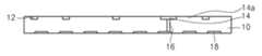
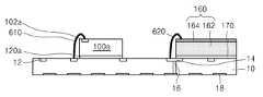
도 1은 본 발명의 일 실시예에 따른 반도체 패키지(1a)를 메인 보드(750)에 부착한 모습을 나타낸 단면도이다.FIG. 1 is a cross-sectional view showing a state where a
도 1을 참조하면, 본 발명의 일 실시예에 따른 반도체 패키지(1a)를 메인 보드(750) 상면의 접속 패드(752a)와 접속 단자(20)를 통하여 이들을 서로 접착시킨 모습을 나타낸다.1, a
반도체 패키지(1a)는 패키지 기판(10) 상에 제1 반도체 칩(100a) 및 도전성 스페이서(140)을 배치하고, 제2 반도체 칩을 상기 제1 반도체 칩(100a) 및 도전성 스페이서(140)에 걸쳐서 적층하는 구조를 가진다. 각각의 반도체 칩의 본딩 패드(102a, 202a, 302a, 402a, 502a)를 연결하는 제2 본딩 와이어(630)를 포함하며, 외부 환경으로부터 반도체 칩들(100a, 200a, 300a, 400a, 500a) 및 본딩 와이어들(610, 630)을 보호하는 몰딩 부재(710)를 포함한다. 또한, 상기 몰딩 부재(710)의 표면 및 패키지 기판(10)의 측면을 덮는 전자파 차폐 부재(730)를 포함한다.The
반도체 패키지(1a)가 메인 보드(750)를 포함하는 전자 장치에 실장된 경우, 반도체 패키지(1a)에서 발생된 전자파가 방출되어 전자 장치에 실장된 다른 전자 부품에 전자파 장해(Electro-Magnetic Interference; EMI)를 줄 수 있다. 이로 인해 반도체 패키지(1a)가 실장된 전자 장치에 전자파 잡음 또는 오동작 등과 같은 장해가 발생되어 제품의 신뢰성이 저하된다. 최근에 개발된 반도체 패키지(1a), 즉 빠른 응답속도 및 고 용량을 갖는 반도체 패키지(1a)의 경우 전자파 방출로 인한 전자파 장해의 문제는 더욱 심각해지고 있다. 따라서, 전자파 차폐 부재(730)는 본 발명의 일 실시예에 따른 반도체 패키지(1a)를 동작시킬 경우 반도체 패키지(1a)의 동작 과정에서 불가피하게 발생되는 전자파가 외부에 영향을 주는 것을 막기 위함이다.When the
전자파 차폐 효과를 높이기 위하여 상기 전자파 차폐 부재(730)는 접속 단자(20)와 전기적으로 연결되도록 형성될 수 있다. 메인 보드(750) 상면의 접속 패드(752a)와 패키지 기판(10)의 하면에 형성된 접지 패드(18) 사이에 접속 단자(20)로서 솔더볼과 같은 도전성 범프를 통하여, 메인 보드(750)와 패키지 기판(10)을 서로 접착시킬 수 있다.The electromagnetic
전자파 차폐 부재(730)는 도전성 스페이서(140)와 전기적으로 연결되며, 상기 도전성 스페이서(140)는 패키지 기판(10) 상면의 접지 패드(14)와 전기적으로 연결되며, 상기 접지 패드(14)는 접지 비아(16)를 통해서 패키지 기판(10) 하면의 접지 패드(18)와 전기적으로 연결되며, 상기 접지 패드(18)는 접속 단자(20)와 전기적으로 연결되며, 상기 접속 단자(20)는 메인 보드(750) 상면의 접속 패드(752a)와 전기적으로 연결된다. 이러한 공정을 통하여 전자파 차폐 부재(730)를 외부에 접지시킬 수 있다.The electromagnetic
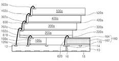
도 2 내지 도 11은 본 발명의 일 실시예에 따른 반도체 패키지(1a)의 제조 순서를 나타낸 도면들이다.2 to 11 are views showing a manufacturing sequence of the
도 2를 참조하면, 패키지 기판(10)은 상면에 신호 패드(12) 및 접지 패드(14)를 가지며 상기 신호 패드(12) 및 접지 패드(14)의 주위를 솔더 레지스트(14a)가 둘러싸고 있다. 패키지 기판(10)의 하면에는 접지 패드(18)를 가진다. 상기 상면의 접지 패드(14)와 하면의 접지 패드(18)를 전기적으로 연결하는 접속 비아(16)를 가진다. 상기 패키지 기판(10)은 앙면 인쇄 회로 기판(double-sided Printed circuit Board)일 수 있다. 물론, 상기 패키지 기판(10)이 양면 인쇄 회로 기판에 한정되는 것은 아니고, 멀티 레이어 인쇄 회로 기판(multi-layer Printed circuit Board)일 수 있다.2, the
도 3을 참조하면, 패키지 기판(10) 상면의 접지 패드(14) 주위를 둘러싸는 솔더 레지스트(14a)의 일부를 제거한 모습을 나타낸다. 솔더 레지스트(14a)의 일부를 제거하면 오픈된 영역(14h)이 나타난다.3, a part of the solder resist 14a surrounding the
도 4를 참조하면, 솔더 레지스트(14a)의 일부를 제거하여 오픈된 영역(14h)에 접착 부재(14b)를 덮는다. 상기 접착 부재(14b)는 접지 패드(14)의 상면을 노출시킨다.Referring to FIG. 4, a part of the solder resist 14a is removed and the
상기 접착 부재(14b)는 DAF(Die attach Film)일 수 있다. DAF는 무기질 접착제와 고분자 접착제로 구분될 수 있다. 고분자의 경우 크게 열경화성 수지(Thermosetting Polymer)와 열가소성 수지(Thermoplastic Polymer)로 나눌 수 있으며, 상기 열경화성 수지의 경우 모노머(Monomer)가 가열 성형된 후 삼차원 망상 구조(Cross-link Structure)를 가지며 재가열하여도 연화되지 않는다. 이와 달리 상기 열가소성 수지의 경우 가열에 의해서 가소성을 나타내는 수지로서 선형 고분자(Linear Polymer)의 구조를 갖는다. 또한, 이 두 가지 성분을 혼합시켜 만든 하이브리드(Hybrid)형도 있다.The
솔더 레지스트(14a)의 일부를 제거하고 오픈된 영역(14h)에 DAF를 덮는 이유는 후술할 도전성 스페이서(140)를 패키지 기판(10)에 접착하는 경우 상기 패키지 기판(10) 상면의 접지 패드(14)와 상기 도전성 스페이서(140)가 전기적으로 연결되도록 하기 위함이다.The reason why the solder resist 14a is partly removed and the DAF is covered in the
종래와 같이 솔더 레지스트(14a)가 존재하는 패키지 기판(10)에 도전성 스페이서(140)를 접착제를 사용하여 접착하는 경우 접착제가 도전성을 가지지 않는다면, 상기 도전성 스페이서(140)와 상기 접지 패드(14)를 전기적으로 이어주기 위하여 본딩 와이어와 같은 도전성 통로를 형성하는 추가적인 공정이 필요할 수 있다.When the
경우에 따라서는, 솔더 레지스트(14a)의 일부만이 아니라 전부를 제거할 수도 있다.In some cases, not all but a part of the solder resist 14a may be removed.
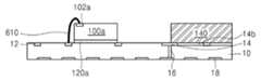
도 5를 참조하면, 패키지 기판(10) 상에 도전성 스페이서(140) 및 제1 반도체 칩(100a)을 배치한다.Referring to FIG. 5, a
최근 전자제품 시장은 휴대용 장치의 수요가 급격하게 증가하고 있으며, 이로 인하여 이들 제품에 실장되는 전자 부품들의 소형화 및 경량화가 지속적으로 요구되고 있다. 이러한 전자 부품들의 소형화 및 경량화를 실현하기 위해서는 실장 부품의 개별 사이즈를 감소시키는 기술뿐만 아니라, 다수의 개별 소자들을 원칩(One-chip)화하는 시스템 온 칩(System On Chip: SOC) 기술 또는 다수의 개별 소자들을 하나의 패키지로 집적하는 시스템 인 패키지(System In Package: SIP) 기술 등이 요구된다.Recently, demand for portable devices has been rapidly increasing in the electronic products market, and there is a continuing demand for miniaturization and weight reduction of electronic components mounted on these products. In order to realize miniaturization and weight reduction of such electronic parts, not only a technique of reducing the individual sizes of the mounting parts but also a system on chip (SOC) technology for making a plurality of individual elements into one chip And a system in package (SIP) technology, which is a system for integrating individual elements into one package.
따라서, 반도체 패키지의 경박단소화를 위하여 본 발명의 실시예에서는 종래 반도체 칩을 일반적으로 적층시키는 구조와는 다르게 패키지 기판(10)의 상면에 제1 반도체 칩(100a)과 도전성 스페이서(140)를 이용하여 고인돌 구조와 같은 형상으로 후속 반도체 칩을 적층시키는 구조를 적용하고 있다.Therefore, unlike the conventional structure in which the semiconductor chip is generally stacked, the
본 발명의 실시예에서 제1 반도체 칩(100a)은 컨트롤러 칩일 수 있다. 메모리 칩 등에 비하여 칩 사이즈가 작은 컨트롤러 칩을 최상단부에 적층하는 방식을 사용하게 되면, 컨트롤러 칩과 패키지 기판(10)과의 본딩 와이어 길이가 길어짐으로 인하여 소자의 동작 특성이 저하되는 문제점이 있었다. 이에 제1 반도체 칩(100a)을 패키지 기판(10) 상에 적층함에 있어서, 컨트롤러 칩을 패키지 기판(10)과 가장 가까운 최하단부에 위치시키는 방법을 사용할 수 있다.In the embodiment of the present invention, the
그러나 앞서 설명한 바와 같이 일반적으로 컨트롤러 칩은 메모리 칩 등에 비하여 칩 사이즈가 작으므로 컨트롤러 칩 위에 바로 메모리 칩 등을 적층하는 경우 구조적인 문제가 발생할 수 있다. 따라서, 패키지 기판(10) 상에 컨트롤러 칩과 지지 구조체인 스페이서를 형성함으로써 상기 문제점을 해결하게 된다.However, as described above, the controller chip generally has a smaller chip size than the memory chip, so that a structural problem may occur when a memory chip or the like is directly stacked on the controller chip. Therefore, the above problem can be solved by forming the controller chip and the spacer, which is the supporting structure, on the
일반적으로 스페이서는 지지 구조체의 역할만을 수행하게 되므로, 실리콘 기판을 가공하여 컨트롤러 칩과 높이를 맞추어 동일 레벨이 되도록 형성하여 고인돌 구조가 될 수 있도록 구성한다.Generally, since the spacers perform only the role of the supporting structure, the silicon substrate is processed so that the height of the silicon chip is the same as the height of the controller chip, so that the silicon substrate is formed to have the same level as that of the controller chip.
본 발명의 일 실시예에 따르면, 상기 스페이서를 도전성 물질, 예를 들어 금속과 같은 전기 전도성이 우수하고 지지 구조체로써 충분한 강도를 가질 수 있는 물질로 구성함으로써, 지지 구조체로서의 역할 및 전기가 흐를 수 있는 통로 역할을 수행할 수 있도록 한다. 따라서, 본 발명의 일 실시예에서는 스페이서를 도전성 스페이서(140)로 칭한다.According to an embodiment of the present invention, the spacer is made of a conductive material, for example, a metal, which is excellent in electrical conductivity and can have sufficient strength as a support structure, thereby functioning as a support structure and capable of flowing electricity To be able to act as a channel. Thus, in one embodiment of the present invention, the spacers are referred to as
또한, 패키지 기판(10) 상면의 접지 패드(14)와 전기적으로 연결될 수 있도록 종래의 접착층을 사용하여 스페이서를 패키지 기판과 접착하는 방식이 아닌, 접지 패드(14) 주위에 접착 부재(14b)를 형성하여 접착하는 방식으로 공정을 진행한다.It is also possible to use an
도전성 스페이서(140)는 지지 구조체의 역할을 수행할 수 있도록 제1 반도체 칩(100a)과의 높이를 동일 레벨로 형성하고, 후속하는 공정에서 몰딩 부재(도 9의 710)로 연결될 수 있도록 접지 패드(14)와 하나 이상 접하는 구조를 형성한다.The
제1 반도체 칩(100a)은 하단부에 제1 접착층(120a)을 사용할 수 있다. 본 발명의 실시예에 따르면 패키지 기판(10) 상면에 접착 부재(14b)가 형성되어 있으므로, 제1 반도체 칩(100a)의 하단부에 제1 접착층(120a)을 형성하는 공정을 생략할 수도 있다. The
제1 반도체 칩(100a)의 상면 본딩 패드(102a)와 패키지 기판(10)의 신호 패드(12)를 연결하는 제1 본딩 와이어(610)를 형성할 수 있다. 앞서 설명한 바와 같이 제1 반도체 칩(100a), 예를 들어 컨트롤러 칩의 경우 일반적으로 제2 반도체 칩(도 6의 200a)인 메모리 칩 등에 비하여 칩 사이즈가 작으므로 후술할 도 21 및 22에서와 같이 제1 반도체 칩(100a)은 제2 반도체 칩(도 6의 200a)에 전부 오버랩될 수 있다. 이 경우 제2 반도체 칩(200a)을 적층한 후 제1 본딩 와이어(610)를 형성하는 공정을 할 수 없으므로, 제1 반도체 칩(100a)의 경우 제2 반도체 칩(도 6의 200a)과는 달리 제1 반도체 칩(100a)을 패키지 기판(10) 상에 배치한 후 제2 반도체 칩(도 6의 200a)을 적층하기 전에 제1 본딩 와이어(610) 형성 공정을 진행할 수 있다.A
도 6을 참조하면, 제2 접착층(220a)의 두께는 다른 접착층의 두께에 비하여 더 두꺼울 수 있다. 그 이유는 다음과 같다.Referring to FIG. 6, the thickness of the second
첫 번째 이유는 제1 반도체 칩(100a)에 형성된 제1 본딩 와이어(610) 루핑(looping) 형태의 변형을 방지하기 위함이다. 앞서 설명한 바와 같이 제1 본딩 와이어(610)를 먼저 형성하게 되고, 상기 제1 본딩 와이어(610)가 제2 반도체 칩(200a) 하부에 위치하게 되므로 인하여, 상기 제1 본딩 와이어(610)의 기계적 변형을 막기 위하여 제2 접착층(220a)의 두께를 제1 본딩 와이어(610)의 루핑으로 인한 두께 이상으로 형성하게 된다.The first reason is to prevent deformation of the looping shape of the
두 번째 이유는 제1 반도체 칩(100a)과 도전성 스페이서(140) 간에 발생할 수 있는 단차를 완하시키기 위함이다. 제1 반도체 칩(100a)의 두께와 맞추어 도전성 스페이서(140)를 제작하더라도 접착층의 유무 및 불가피한 이유로 인하여 단차가 형성될 수 있고 이 경우 상기 제2 반도체 칩(200a)의 구조적 안정성에 문제가 발생할 수 있으므로, 제2 접착층(220a)이 단차를 완화해주는 역할을 수행할 수 있다.The second reason is to relieve a step that may occur between the
제2 반도체 칩(200a)은 도전성 스페이서(140)의 일부만을 덮을 수 있다. 도전성 스페이서(140)는 전자파 차폐 부재(도 10의 730)와 전기적으로 연결되어야 하므로 앞서 설명한 바와 같이 패키지 기판(10)의 가장자리와 맞닿을 수 있도록 배치된다. 따라서 제2 반도체 칩(200a)은 도전성 스페이서(140)의 전부를 덮는 것이 아닌 일부만을 덮도록 형성된다.The
도 7을 참조하면, 제2 반도체 칩(200a) 위에 제3 내지 제5 반도체 칩들(300a, 400a, 500a)을 적층한 모습을 나타낸다.Referring to FIG. 7, third to
상부 반도체 칩들(200a, 300a, 400a, 500a)이 하부 제1 반도체 칩(100a) 상에 복수 개가 적층될 수 있다. 복수 개의 상부 반도체 칩들(200a, 300a, 400a, 500a)은 각각 패키지 기판에 수평 방향으로 소정 거리만큼 쉬프트되어 아래에 있는 반도체 칩 상면의 일부분에 형성된 본딩 패드(102a, 202a, 302a, 402a)가 노출되도록 하부 반도체 칩 상에 순차적으로 적층될 수 있다.A plurality of
다수의 개별 소자들을 하나의 패키지로 집적하는 시스템 인 패키지 기술에 있어서, 반도체 칩의 개수는 반도체 패키지의 용도에 따라 다를 수 있다. 본 발명의 기술적 사상은 반도체 칩의 개수에 의해 구속되는 것은 아니다. 즉, 반도체 칩들이 더 많이 적층되어 있을 수도 있고, 더 적게 적층되어 있을 수도 있다.In package technology, which is a system for integrating a plurality of individual elements into one package, the number of semiconductor chips may vary depending on the use of the semiconductor package. The technical idea of the present invention is not limited by the number of semiconductor chips. That is, the semiconductor chips may be stacked more or less.
도 8을 참조하면, 제2 본딩 와이어(630)를 형성하여 복수의 상부 반도체 칩들(200a, 300a, 400a, 500a) 각각의 본딩 패드(202a, 302a, 402a, 502a)와 패키지 기판(10)의 신호 패드(12) 사이를 연결할 수 있다.Referring to FIG. 8, a
제3 반도체 칩(300a)은 제2 반도체 칩(200a) 상에 적층될 수 있으며, 제3 접착층(320a)에 의해 제2 반도체 칩(200a)에 접착될 수 있다. 일 실시예에 있어서, 제3 접착층(320a)은 제3 반도체 칩(300a)의 저면을 커버하는 접착 필름 혹은 접착 시트를 포함할 수 있다. 이와는 달리, 제3 접착층(320a)은 제3 반도체 칩(300a)의 저면에 적어도 하나 이상으로 형성된 도전성 범프들을 포함할 수도 있다. 제3 반도체 칩(300a)은 상부에 적어도 하나 이상의 본딩 패드(302a)를 포함할 수 있다. 예시적인 실시예들에 있어서, 본딩 패드(302a)는 제2 본딩 와이어(630)에 의해 제2 반도체 칩(200a)에 형성된 본딩 패드(202a)에 각각 전기적으로 연결될 수 있다.The
상기와 같이 반도체 칩을 계단 형태로 적층하기 위하여 RDL(Redistributed Layer)을 형상할 수 있다. 반도체 칩의 패드가 칩의 중앙에 위치하고 있는 경우 적층 시 패키지가 복잡해지고 본딩 와이어의 길이가 길어져 소자 특성이 저하되는 등의 문제가 있다. 이를 해결하기 위해 본딩 패드의 위치를 도면에서와 같이 칩의 중앙에서 가장자리로 변경하여 칩의 적층을 용이하게 하는 공정이다. 반도체 패키지 공정에서 본딩 와이어의 루핑 자유도를 높여준다.In order to stack the semiconductor chips in a stepwise manner as described above, a redistributed layer (RDL) may be formed. When the pad of the semiconductor chip is located at the center of the chip, there is a problem that the package becomes complicated during stacking, the length of the bonding wire becomes long, and the device characteristics are deteriorated. In order to solve this problem, the position of the bonding pads is changed from the center to the edge of the chip as shown in the drawing to facilitate stacking of the chips. Thereby increasing the degree of freedom of looping of the bonding wire in the semiconductor package process.
도 9를 참조하면, 패키지 기판(10) 및 반도체 칩들(100a, 200a, 300a, 400a, 500a)을 덮고 도전성 스페이서(140)의 일부를 노출시키는 몰딩 부재(710)를 형성한다.Referring to FIG. 9, a
상기 몰딩 부재(710)는 패키지 기판(10)의 상면에 형성되어, 반도체 칩들(100a, 200a, 300a, 400a, 500a), 본딩 와이어들(610, 630) 및 도전성 스페이서(140)를 덮는다. 상기 몰딩 부재(710)는 외부 환경으로부터 반도체 칩들(100a, 200a, 300a, 400a, 500a) 및 본딩 와이어들(610, 630)을 보호한다. 본 실시예에서, 몰딩 부재(710)는 에폭시 몰딩 컴파운드(Epoxy Molding Compound: EMC)를 포함할 수 있다.The
일반적인 경우 상기 몰딩 부재(710)는 패키지 기판(10)의 상면에 배치된 것들을 모두 덮는 형태로 형성되나, 본 발명의 경우 도전성 스페이서(140)의 일부가 노출되는 형태로 형성된다. 이는 도전성 스페이서(140)와 전자파 차폐 부재(도 10의 730)가 전기적으로 연결되어 접지 통로 역할을 하여야 하기 때문이다.In general, the
도 10을 참조하면, 전자파 차폐 부재(730)는 몰딩 부재(710)를 커버하고, 패키지 기판(10) 상에 배치된 도전성 스페이서(140)에 전기적으로 연결될 수 있다.10, the electromagnetic
전자파 차폐 부재(730)는 상기 몰딩 부재(710)의 상면 및 측면을 커버할 수 있다. 즉, 전자파 차폐 부재(730)는 몰딩 부재(710)의 상면, 측면 및 패키지 기판(10)의 측면을 커버할 수 있다. 이때, 패키지 기판(10)의 상면에 배치된 도전성 스페이서(140)의 몰딩 부재(710)에서 노출된 일부가 전자파 차폐 부재(730)에 접촉하여 이에 전기적으로 연결될 수 있다. 전자파 차폐 부재(730)는 도전성 물질을 포함할 수 있다. 예를 들어, 상기 도전성 물질은 구리, 은 등과 같은 금속을 포함할 수 있다.The electromagnetic
전자파 차폐 효과를 높이기 위하여 상기 전자파 차폐 부재(730)는 접속 단자(20)와 전기적으로 연결되도록 형성될 수 있다. 본 발명에서는 상기 전자파 차폐 부재(730)가 도전성 스페이서(140)와 전기적으로 연결됨으로써, 접속 단자(20)와 전기적으로 연결될 수 있도록 형성된다.The electromagnetic
전자파 차폐 부재(730)는 금속 박막으로 형성될 수 있다. 이 경우 금속 박막은 스프레이 코팅법, 전해 도금법, 무전해 도금법, 스퍼터링법과 같은 박막 증착 방법으로 형성될 수 있다.The electromagnetic
도 11을 참조하면, 패키지 기판(10) 하면의 접지 패드(18)에 접속 단자(20)을 형성한 반도체 패키지(1a)를 나타낸다. 예시적인 실시예들에 있어서, 패키지 기판(10)의 하면에 형성된 접지 패드(18)에 접속 단자(20)로서 솔더볼과 같은 도전성 범프를 형성할 수 있다.11 shows a
전자파 차폐 부재(730)는 도전성 스페이서(140)와 전기적으로 연결되며, 상기 도전성 스페이서(140)는 패키지 기판(10) 상면의 접지 패드(14)와 전기적으로 연결되며, 상기 접지 패드(14)는 접지 비아(16)를 통해서 패키지 기판(10) 하면의 접지 패드(18)와 전기적으로 연결되며, 상기 접지 패드(18)는 접속 단자(20)와 전기적으로 연결된다.The electromagnetic
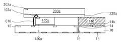
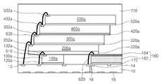
도 12는 본 발명의 다른 실시예에 따른 반도체 패키지(2a)를 메인 보드(750)에 부착한 모습을 나타낸 단면도이다.12 is a cross-sectional view showing a state in which a
도 12를 참조하면, 본 발명의 다른 실시예에 따른 반도체 패키지(2a)를 메인 보드(750) 상면의 접속 패드(752a)와 접속 단자(20)를 통하여 이들을 서로 접착시킨 모습을 나타낸다.12, a
반도체 패키지(2a)는 패키지 기판(10) 상에 제1 반도체 칩(100a) 및 스페이서 구조체(160)를 배치하고, 제2 반도체 칩을 상기 제1 반도체 칩(100a) 및 스페이서 구조체(160)에 걸쳐서 적층하는 구조를 가진다. 각각의 반도체 칩의 본딩 패드(102a, 202a, 302a, 402a, 502a)를 연결하는 제2 본딩 와이어(630)를 포함하며, 외부 환경으로부터 반도체 칩들(100a, 200a, 300a, 400a, 500a) 및 본딩 와이어들(610, 620, 630)을 보호하는 몰딩 부재(710)를 포함한다. 또한, 상기 몰딩 부재(710)의 표면 및 패키지 기판(10)의 측면을 덮는 전자파 차폐 부재(730)를 포함한다.The
전자파 차폐 효과를 높이기 위하여 상기 전자파 차폐 부재(730)는 접속 단자(20)와 전기적으로 연결되도록 형성될 수 있다. 메인 보드(750) 상면의 접속 패드(752a)와 패키지 기판(10)의 하면에 형성된 접지 패드(18) 사이에 접속 단자(20)로서 솔더볼과 같은 도전성 범프를 통하여, 메인 보드(750)와 패키지 기판(10)을 서로 접착시킬 수 있다.The electromagnetic
상기 전자파 차폐 부재(730)는 도전성 부재(164)와 전기적으로 연결되며, 상기 도전성 부재(164)는 제3 본디 와이어(620)와 전기적으로 연결되며, 상기 제3 본딩 와이어(630)는 패키지 기판(10) 상면의 접지 패드(14)와 전기적으로 연결되며, 상기 상면의 접지 패드(14)는 접지 비아(16)를 통해서 패키지 기판(10) 하면의 접지 패드(18)와 전기적으로 연결되며, 상기 패키지 기판(10) 하면의 접지 패드(18)는 접속 단자(20)와 전기적으로 연결되며, 상기 접속 단자(20)는 메인 보드(750) 상면의 접속 패드(752a)와 전기적으로 연결된다. 이러한 공정을 통하여 전자파 차폐 부재(730)를 외부에 접지시킬 수 있다.The electromagnetic
도 13 내지 도 20은 본 발명의 다른 실시예에 따른 반도체 패키지(2a)의 제조 순서를 나타낸 도면들이다.13 to 20 are views showing a manufacturing sequence of the
여기서는, 앞서 반도체 패키지(도 1의 1a)에서 설명한 사항에 대하여는 실질적으로 동일하므로, 반복 설명은 생략하고 차이점에 대하여만 설명하도록 한다.Here, since the matters described above in the semiconductor package (1a in FIG. 1) are substantially the same, repetitive description will be omitted and only difference will be described.
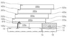
도 13을 참조하면, 패키지 기판(10) 상에 도전성 부재(164)가 상면에 형성된 스페이서(162) 및 제1 반도체 칩(100a)을 배치한다.Referring to FIG. 13, a
패키지 기판(10)은 상면에 신호 패드(12) 및 접지 패드(14)를 가지며 상기 신호 패드(12) 및 접지 패드(14)의 주위를 솔더 레지스트(14a)가 둘러싸고 있다. 패키지 기판(10)의 하면에는 접속 단자(20)를 가진다. 상기 접지 패드(14)와 상기 접속 단자(20)를 전기적으로 연결하는 접속 비아(16)를 가진다. 상기 패키지 기판(10)은 앙면 인쇄 회로 기판일 수 있다. 물론, 상기 패키지 기판(10)이 양면 인쇄 회로 기판에 한정되는 것은 아니고, 멀티 레이어 인쇄 회로 기판일 수 있다.The
본 발명의 다른 실시예에 따르면, 패키지 기판(10) 상에 배치되는 상기 스페이서(162)의 상면에 도전성 부재(164), 예를 들어 금속과 같은 전기 전도성이 우수한 물질을 금속 박막 형성 방법으로 형성한다. 이 경우 금속 박막은 스프레이 코팅법, 전해 도금법, 무전해 도금법, 스퍼터링법과 같은 박막 증착 방법으로 형성될 수 있다. 상기 도전성 부재(164)는 전기가 흐를 수 있는 통로 역할을 수행할 수 있도록 한다.According to another embodiment of the present invention, a
스페이서 구조체(160)는 지지 구조체의 역할을 수행할 수 있도록 제1 반도체 칩(100a)과의 높이를 동일 레벨로 형성하고, 후속하는 공정에서 몰딩 부재(도 18의 710)에 의해 스페이서 구조체(160)의 일부분이 노출될 수 있도록 패키지 기판(10)의 가장자리 부분에 스페이서 구조체(160)의 일 부분이 맞닿는 구조로 형성한다. 스페이서(162)는 일반적으로 사용되는 실리콘 기판 등일 수 있다.The
제1 반도체 칩(100a) 및 스페이서(162)의 하단부에 접착층을 형성할 수 있다. 본 발명의 실시예에 따르면 앞서 설명한 반도체 패키지(도 1의 1a)와 다르게 패키지 기판(10) 상에 접착 부재(도 1의 14b)가 형성되지 않으므로, 하단부에 접착층을 통하여 패키지 기판과 접착한다. 스페이서(162)의 하단부에도 스페이서 접착층(170)을 형성한다.An adhesive layer can be formed on the lower end portions of the
도 14를 참조하면, 제1 반도체 칩(100a) 및 스페이서 구조체(160)에 본딩 와이어를 형성하는 모습을 나타낸다.Referring to FIG. 14, a bonding wire is formed on the
제1 반도체 칩(100a)의 상면 본딩 패드(102a)와 패키지 기판(10)의 신호 패드(12)를 연결하는 제1 본딩 와이어(610)를 형성할 수 있다. 또한, 스페이서(162) 상에 형성된 도전성 부재(164)와 접지 패드(14)를 연결하는 제3 본딩 와이어(620)를 형성할 수 있다. 앞서 설명한 반도체 패키지(도 1의 1a)와 다르게 본 실시예에서는 스페이서(162) 자체는 실리콘 기판 등 도전성 물질이 아닐 수 있으므로 접지 패드(14)와 도전성 부재(164)가 직접적으로 연결될 수 없는 바, 제3 본딩 와이어(620)를 통하여 도전성 부재(164)와 접지 패드(14)를 전기적으로 연결한다.A
앞서 설명한 바와 같이 제1 반도체 칩(100a), 예를 들어 컨트롤러 칩의 경우 일반적으로 제2 반도체 칩(도 15의 200a)인 메모리 칩 등에 비하여 칩 사이즈가 작으므로 후술할 도 21 및 22에서와 같이 제1 반도체 칩(100a)은 제2 반도체 칩(도 15의 200a)에 전부 오버랩될 수 있다. 이 경우 제2 반도체 칩(도 15의 200a)을 적층한 후 제1 본딩 와이어(610) 및 제3 본딩 와이어(630)를 형성하는 공정을 할 수 없으므로, 제1 반도체 칩(100a)의 경우 제2 반도체 칩(도 15의 200a)과는 달리 제1 반도체 칩(100a)을 패키지 기판(10) 상에 배치한 후 제2 반도체 칩(도 15의 200a)을 적층하기 전에 제1 본딩 와이어(610) 형성 공정을 진행할 수 있다.As described above, since the chip size is smaller than that of the
도 15를 참조하면, 제1 반도체 칩(100a) 및 스페이서 구조체(160)의 상부에 제2 반도체 칩(200a)을 적층하는 모습을 나타낸다. 앞서 실시예의 반도체 패키지(도 1의 1a)와 마찬가지로 제1 본딩 와이어(610) 및 제3 본딩 와이어(620)의 루핑 형상이 변형되지 않고, 제1 반도체 칩(100a)과 스페이서 구조체(160) 사이의 단차를 줄이기 위하여 제2 접착층(220a)의 두께를 다른 접착층에 비하여 두껍게 형성할 수 있다.Referring to FIG. 15, a
도 16을 참조하면, 제2 반도체 칩(200a) 위에 제3 내지 제5 반도체 칩들(300a, 400a, 500a)을 적층한 모습을 나타낸다.Referring to FIG. 16, a
상부 반도체 칩들(200a, 300a, 400a, 500a)이 하부 제1 반도체 칩(100a) 상에 복수 개가 적층될 수 있다. 복수 개의 상부 반도체 칩들(200a, 300a, 400a, 500a)은 각각 패키지 기판(10)에 수평 방향으로 소정 거리만큼 쉬프트되어 아래에 있는 반도체 칩 상면의 일부분에 형성된 본딩 패드(102a, 202a, 302a, 402a)가 노출되도록 하부 반도체 칩 상에 순차적으로 적층될 수 있다.A plurality of
도 17을 참조하면, 제2 본딩 와이어(630)를 형성하여 복수의 상부 반도체 칩들(200a, 300a, 400a, 500a) 각각의 본딩 패드(202a, 302a, 402a, 502a)와 패키지 기판(10)의 신호 패드(12) 사이를 연결할 수 있다.Referring to FIG. 17, a
도 18을 참조하면, 패키지 기판(10) 및 반도체 칩들(100a, 200a, 300a, 400a, 500a)을 덮고 스페이서 구조체(160)의 일부를 노출시키는 몰딩 부재(710)를 형성한다.18, a
도 19를 참조하면, 전자파 차폐 부재(730)는 몰딩 부재(710)를 커버하고, 도전성 부재(164)에 전기적으로 연결될 수 있다.19, the electromagnetic
도 20을 참조하면, 패키지 기판(10) 하면의 접지 패드(18)에 접속 단자(20)을 형성한 반도체 패키지(2a)를 나타낸다. 예시적인 실시예들에 있어서, 패키지 기판(10)의 하면에 형성된 접지 패드(18)에 접속 단자(20)로서 솔더볼과 같은 도전성 범프를 형성할 수 있다.20 shows a
전자파 차폐 부재(730)는 도전성 부재(164)와 전기적으로 연결되며, 상기 도전성 부재(164)는 제3 본디 와이어(620)와 전기적으로 연결되며, 상기 제3 본딩 와이어(630)는 패키지 기판(10) 상면의 접지 패드(14)와 전기적으로 연결되며, 상기 상면의 접지 패드(14)는 접지 비아(16)를 통해서 패키지 기판(10) 하면의 접지 패드(18)와 전기적으로 연결되며, 상기 패키지 기판(10) 하면의 접지 패드(18)는 접속 단자(20)와 전기적으로 연결된다.The electromagnetic
도 21 및 도 22는 본 발명의 일 실시예에 따른 반도체 패키지(1a)를 개략적으로 나타내는 평면 배치도이다.21 and 22 are plan layout diagrams schematically showing a
도 21을 참조하면, 패키지 기판(10) 상에서 제2 반도체 칩(200a) 및 도전성 스페이서(140)의 상대적인 위치를 나타낸 모습이다. 도전성 스페이서(140)의 일부는 전자파 차폐 부재(730)와 접하고, 상기 도전성 스페이서(140)는 제2 반도체 칩(200a)의 지지 구조체로서의 역할도 수행하므로 제1 방향(y 방향)으로 전자파 차폐 부재(730)와 접하도록 위치할 수 있다.Referring to FIG. 21, the relative positions of the
앞서 설명한 바와 같이 일반적으로 컨트롤러 칩은 메모리 칩 등에 비하여 칩 사이즈가 작으므로 컨트롤러 칩 위에 바로 메모리 칩 등을 적층하는 경우 도면과 같은 배치가 된다.As described above, in general, the controller chip has a smaller chip size than a memory chip. Therefore, when the memory chip or the like is directly stacked on the controller chip, the arrangement is the same as that shown in the drawing.
도면에 나타내지는 않았지만, 스페이서(도 20의 162)의 상면에 도전성 부재(도 20의 164)가 형성된 경우에 있어서도 마찬가지의 배치를 가질 수 있다.Although not shown in the drawings, the same arrangement can be provided when the conductive member (164 of FIG. 20) is formed on the upper surface of the spacer (162 of FIG. 20).
도 22를 참조하면, 패키지 기판(10) 상에서 제2 반도체 칩(200a) 및 도전성 스페이서(140)의 상대적인 위치를 나타낸 모습이다. 도전성 스페이서(140)의 일부는 전자파 차폐 부재(730)와 접하고, 상기 도전성 스페이서(140)는 제2 반도체 칩(200a)의 지지 구조체로서의 역할도 수행하므로 제2 방향(x 방향)으로 전자파 차폐 부재(730)와 접하도록 위치할 수 있다.Referring to FIG. 22, the relative positions of the
도면에 나타내지는 않았지만, 스페이서(도 20의 162)의 상면에 도전성 부재(도 20의 164)가 형성된 경우에 있어서도 마찬가지의 배치를 가질 수 있다.Although not shown in the drawings, the same arrangement can be provided when the conductive member (164 of FIG. 20) is formed on the upper surface of the spacer (162 of FIG. 20).
도 23은 본 발명의 실시예에 따른 반도체 패키지(1a, 2a)를 포함하는 메모리 모듈을 나타내는 평면도이다.23 is a plan view showing a memory module including
도 23을 참조하면, 메모리 모듈(1100)은 모듈 기판(1110)과, 상기 모듈 기판(1110)에 부착된 복수의 반도체 패키지(1120)를 포함한다.Referring to FIG. 23, a
반도체 패키지(1120)는 본 발명의 일 실시예에 따른 반도체 패키지(1a, 2a)를 포함한다. 예를 들면, 반도체 패키지(1120)는 도 1 및 도 12에 예시한 반도체 패키지(1a, 2a)를 포함할 수 있다.The
모듈 기판(1110)의 일측에는 메인 보드의 소켓에 끼워질 수 있는 접속부(1130)가 배치된다. 모듈 기판(1110) 상에는 세라믹 디커플링 커패시터(1140)가 배치된다. 본 발명에 의한 메모리 모듈(1100)은 도 23에 예시된 구성에만 한정되지 않고 다양한 형태로 제작될 수 있다.At one side of the
도 24는 본 발명의 실시예에 따른 반도체 패키지(1a, 2a)를 포함하는 시스템을 나타내는 구성도이다.24 is a configuration diagram showing a system including
도 24를 참조하면, 시스템(1200)은 제어기(1210), 입/출력 장치(1220), 기억 장치(1230), 및 인터페이스(1240)를 포함한다. 시스템(1200)은 모바일 시스템 또는 정보를 전송하거나 전송받는 시스템일 수 있다. 일부 실시예에서, 상기 모바일 시스템은 PDA, 휴대용 컴퓨터(portable computer), 웹 타블렛(web tablet), 무선 폰(wireless phone), 모바일 폰(mobile phone), 디지털 뮤직 플레이어(digital music player) 또는 메모리 카드(memory card)이다. 제어기(1210)는 시스템(1200)에서의 실행 프로그램을 제어하기 위한 것으로, 마이크로프로세서(microprocessor), 디지털 신호 처리기(digital signal processor), 마이크로콘트롤러(microcontroller), 또는 이와 유사한 장치로 이루어질 수 있다. 입/출력 장치(1220)는 시스템(1200)의 데이터를 입력 또는 출력하는데 이용될 수 있다. 시스템(1200)은 입/출력 장치(1220)를 이용하여 외부 장치, 예컨대 개인용 컴퓨터 또는 네트워크에 연결되고, 외부 장치와 서로 데이터를 교환할 수 있다. 입/출력 장치(1220)는, 예를 들면 키패드(keypad), 키보드(keyboard), 또는 표시장치(display)일 수 있다.Referring to FIG. 24, a
기억 장치(1230)는 제어기(1210)의 동작을 위한 코드 및/또는 데이터를 저장하거나, 제어기(1210)에서 처리된 데이터를 저장할 수 있다. 기억 장치(1230)는 본 발명의 실시예에 따른 반도체 패키지를 포함한다. 예를 들면, 기억 장치(1230)는 도 1 및 도 12에 예시한 반도체 패키지(1a, 2a)를 포함할 수 있다.The
인터페이스(1240)는 시스템(1200)과 외부의 다른 장치 사이의 데이터 전송 통로일 수 있다. 제어기(1210), 입/출력 장치(1220), 기억 장치(1230), 및 인터페이스(1240)는 버스(1250)를 통해 서로 통신할 수 있다. 시스템(1200)은 모바일 폰(mobile phone), MP3 플레이어, 네비게이션(navigation), 휴대용 멀티미디어 재생기(portable multimedia player: PMP), 고상 디스크(solid state disk: SSD), 또는 가전 제품(household appliances)에 이용될 수 있다.The
도 25는 본 발명의 실시예에 따른 반도체 패키지(1a, 2a)를 포함하는 메모리 카드를 나타내는 구성도이다.25 is a configuration diagram showing a memory card including the semiconductor packages 1a and 2a according to the embodiment of the present invention.
도 25를 참조하면, 메모리 카드(1300)는 기억 장치(1310) 및 메모리 제어기(1320)를 포함한다.25, the
기억 장치(1310)는 데이터를 저장할 수 있다. 일부 실시예에서, 기억 장치(1310)는 전원 공급이 중단되어도 저장된 데이터를 그대로 유지할 수 있는 비휘발성 특성을 갖는다. 기억 장치(1310)는 본 발명의 실시예에 따른 반도체 패키지를 포함한다. 예를 들면, 기억 장치(1310)는 도 1 및 도 12에 예시한 반도체 패키지(1a, 2a)를 포함할 수 있다.
메모리 제어기(1320)는 호스트(1330)의 읽기/쓰기 요청에 응답하여 상기 기억 장치(1310)에 저장된 데이터를 읽거나, 기억 장치(1310)의 데이터를 저장할 수 있다.The
이상, 본 발명을 바람직한 실시예를 들어 상세하게 설명하였으나, 본 발명은 상기 실시예에 한정되지 않고, 본 발명의 기술적 사상 및 범위 내에서 당 분야에서 통상의 지식을 가진 자에 의하여 여러 가지 변형 및 변경이 가능하다.While the present invention has been particularly shown and described with reference to exemplary embodiments thereof, it is to be understood that the present invention is not limited to the disclosed exemplary embodiments, and various changes and modifications may be made by those skilled in the art without departing from the scope and spirit of the invention. Change is possible.
10: 패키지 기판,14: 접지 패드,16: 접지 비아
100a: 제1 반도체 칩,140: 도전성 스페이서,160: 스페이서
200a: 제2 반도체 칩
610: 제1 본딩 와이어
710: 몰딩 부재,730: 전자파 차폐 부재10: package substrate, 14: ground pad, 16: ground via
100a: first semiconductor chip, 140: conductive spacer, 160: spacer
200a: second semiconductor chip
610: first bonding wire
710: molding member, 730: electromagnetic wave shielding member
Claims (10)
Translated fromKorean상기 패키지 기판 상에 배치되는 도전성 스페이서 및 제1 반도체 칩;
상기 도전성 스페이서 및 제1 반도체 칩 상에 걸쳐서 적층되는 제2 반도체 칩;
상기 패키지 기판, 제1 반도체 칩 및 제2 반도체 칩을 덮고 상기 도전성 스페이서의 일부를 노출시키는 몰딩 부재; 및
상기 몰딩 부재의 표면을 덮는 전자파 차폐 부재를 포함하는 것을 특징으로 하는 반도체 패키지.A package substrate comprising a ground pad;
A conductive spacer and a first semiconductor chip disposed on the package substrate;
A second semiconductor chip stacked over the conductive spacer and the first semiconductor chip;
A molding member covering the package substrate, the first semiconductor chip and the second semiconductor chip and exposing a part of the conductive spacer; And
And an electromagnetic wave shielding member covering the surface of the molding member.
상기 몰딩 부재에서 노출되는 도전성 스페이서의 일부에 상기 전자파 차폐 부재가 전기적으로 연결되는 것을 특징으로 하는 반도체 패키지.The method according to claim 1,
And the electromagnetic wave shielding member is electrically connected to a part of the conductive spacer exposed in the molding member.
상기 도전성 스페이서의 하부면은 상기 접지 패드에 전기적으로 연결되는 것을 특징으로 하는 반도체 패키지.The method according to claim 1,
And a lower surface of the conductive spacer is electrically connected to the ground pad.
상기 접지 패드의 주위에 배치되며, 상기 도전성 스페이서를 접착시키는 접착 부재를 포함하는 것을 특징으로 하는 반도체 패키지.The method according to claim 1,
And an adhesive member disposed around the ground pad and adhering the conductive spacer.
상기 전자파 차폐 부재는 상기 몰딩 부재의 표면 및 상기 패키지 기판의 측면을 덮는 것을 특징으로 하는 반도체 패키지.The method according to claim 1,
Wherein the electromagnetic wave shielding member covers a surface of the molding member and a side surface of the package substrate.
상기 패키지 기판 상에 배치되는 스페이서;
상기 스페이서 상에 형성되는 도전성 부재;
상기 스페이서와 이격되도록 상기 패키지 기판 상에 배치되는 제1 반도체 칩;
상기 스페이서 및 제1 반도체 칩 상에 걸쳐서 적층되는 제2 반도체 칩;
상기 패키지 기판 및 상기 반도체 칩을 덮고 상기 도전성 부재의 일부를 노출시키는 몰딩 부재; 및
상기 몰딩 부재의 표면을 덮는 전자파 차폐 부재를 포함하는 것을 특징으로 하는 반도체 패키지.A package substrate comprising a ground pad;
A spacer disposed on the package substrate;
A conductive member formed on the spacer;
A first semiconductor chip disposed on the package substrate so as to be spaced apart from the spacer;
A second semiconductor chip stacked over the spacer and the first semiconductor chip;
A molding member covering the package substrate and the semiconductor chip and exposing a part of the conductive member; And
And an electromagnetic wave shielding member covering the surface of the molding member.
상기 몰딩 부재에서 노출되는 도전성 부재의 일부는 상기 전자파 차폐 부재에 의해 덮이는 것을 특징으로 하는 반도체 패키지.The method according to claim 6,
And a part of the conductive member exposed in the molding member is covered by the electromagnetic wave shielding member.
상기 도전성 부재와 상기 접지 패드를 전기적으로 연결하는 본딩 와이어를 더 포함하는 것을 특징으로 하는 반도체 패키지.The method according to claim 6,
Further comprising a bonding wire electrically connecting the conductive member to the ground pad.
상기 전자파 차폐 부재는 상기 몰딩 부재의 표면 및 상기 패키지 기판의 측면을 덮는 것을 특징으로 하는 반도체 패키지.The method according to claim 6,
Wherein the electromagnetic wave shielding member covers a surface of the molding member and a side surface of the package substrate.
상기 접속 패드와 전기적으로 연결되도록 상기 메인 보드 상에 배치되는 반도체 패키지를 포함하는 전자 장치에 있어서,
상기 반도체 패키지는
접지 패드를 포함하는 패키지 기판;
상기 패키지 기판 상에 배치되는 도전성 스페이서 및 제1 반도체 칩;
상기 도전성 스페이서 및 제1 반도체 칩 상에 걸쳐서 적층되는 제2 반도체 칩;
상기 패키지 기판 및 상기 반도체 칩을 덮고 상기 도전성 스페이서의 일부를 노출시키는 몰딩 부재; 및
상기 몰딩 부재 표면 및 상기 패키지 기판의 측면을 덮는 전자파 차폐 부재를 포함하는 것을 특징으로 하는 전자 장치.A main board including a connection pad; And
And a semiconductor package disposed on the main board to be electrically connected to the connection pad,
The semiconductor package
A package substrate comprising a ground pad;
A conductive spacer and a first semiconductor chip disposed on the package substrate;
A second semiconductor chip stacked over the conductive spacer and the first semiconductor chip;
A molding member covering the package substrate and the semiconductor chip and exposing a part of the conductive spacer; And
And an electromagnetic wave shielding member covering the surface of the molding member and the side surface of the package substrate.
Priority Applications (2)
| Application Number | Priority Date | Filing Date | Title |
|---|---|---|---|
| KR1020140119369AKR102210332B1 (en) | 2014-09-05 | 2014-09-05 | Semiconductor package |
| US14/723,721US9355969B2 (en) | 2014-09-05 | 2015-05-28 | Semiconductor package |
Applications Claiming Priority (1)
| Application Number | Priority Date | Filing Date | Title |
|---|---|---|---|
| KR1020140119369AKR102210332B1 (en) | 2014-09-05 | 2014-09-05 | Semiconductor package |
Publications (2)
| Publication Number | Publication Date |
|---|---|
| KR20160029595Atrue KR20160029595A (en) | 2016-03-15 |
| KR102210332B1 KR102210332B1 (en) | 2021-02-01 |
Family
ID=55438207
Family Applications (1)
| Application Number | Title | Priority Date | Filing Date |
|---|---|---|---|
| KR1020140119369AActiveKR102210332B1 (en) | 2014-09-05 | 2014-09-05 | Semiconductor package |
Country Status (2)
| Country | Link |
|---|---|
| US (1) | US9355969B2 (en) |
| KR (1) | KR102210332B1 (en) |
Cited By (4)
| Publication number | Priority date | Publication date | Assignee | Title |
|---|---|---|---|---|
| KR20170143124A (en)* | 2016-06-20 | 2017-12-29 | 삼성전자주식회사 | Semiconductor package |
| US10319702B2 (en) | 2017-08-09 | 2019-06-11 | Samsung Electronics Co., Ltd. | Semiconductor packages |
| KR20190111414A (en)* | 2018-03-22 | 2019-10-02 | 삼성전자주식회사 | Semiconductor package |
| KR20210129895A (en)* | 2020-04-21 | 2021-10-29 | 삼성전자주식회사 | Semiconductor package and method of manufacturing the semiconductor package |
Families Citing this family (17)
| Publication number | Priority date | Publication date | Assignee | Title |
|---|---|---|---|---|
| US9627367B2 (en) | 2014-11-21 | 2017-04-18 | Micron Technology, Inc. | Memory devices with controllers under memory packages and associated systems and methods |
| JP2016178196A (en)* | 2015-03-19 | 2016-10-06 | 株式会社東芝 | Semiconductor device and manufacturing method thereof |
| JP2016192447A (en)* | 2015-03-30 | 2016-11-10 | 株式会社東芝 | Semiconductor device |
| TWI606563B (en)* | 2016-04-01 | 2017-11-21 | 力成科技股份有限公司 | Thin stacked chip package and the method for manufacturing the same |
| KR20180004413A (en)* | 2016-07-04 | 2018-01-12 | 삼성전자주식회사 | Semiconductor package and method for fabricating the same |
| KR102592640B1 (en) | 2016-11-04 | 2023-10-23 | 삼성전자주식회사 | Semiconductor package and method of manufacturing the semiconductor package |
| US10847505B2 (en) | 2018-04-10 | 2020-11-24 | Taiwan Semiconductor Manufacturing Company, Ltd. | Multi-chip semiconductor package |
| KR102592329B1 (en) | 2018-06-26 | 2023-10-20 | 삼성전자주식회사 | Fabrication method of semiconductor package |
| KR102571267B1 (en)* | 2018-09-19 | 2023-08-29 | 에스케이하이닉스 주식회사 | Stack package including partially stacked semiconductor dies |
| JP7247733B2 (en)* | 2019-04-25 | 2023-03-29 | 株式会社レゾナック | Manufacturing method of semiconductor device having dolmen structure |
| US11764161B2 (en)* | 2019-12-06 | 2023-09-19 | Micron Technology, Inc. | Ground connection for semiconductor device assembly |
| JP7532885B2 (en)* | 2020-05-15 | 2024-08-14 | 株式会社レゾナック | Semiconductor device, manufacturing method thereof, and structure used in manufacturing the semiconductor device |
| KR102840204B1 (en) | 2020-08-19 | 2025-08-01 | 삼성전자주식회사 | Semiconductor package |
| KR102853084B1 (en) | 2020-10-26 | 2025-09-02 | 삼성전자주식회사 | Semiconductor package including semiconductor chips |
| US11742322B2 (en)* | 2021-01-20 | 2023-08-29 | Taiwan Semiconductor Manufacturing Company, Ltd. | Integrated fan-out package having stress release structure |
| JP2023184027A (en)* | 2022-06-17 | 2023-12-28 | キオクシア株式会社 | Semiconductor device and semiconductor device manufacturing method |
| WO2025063210A1 (en)* | 2023-09-22 | 2025-03-27 | 株式会社レゾナック | Die attachment film, dicing die bonding film, and semiconductor device manufacturing method |
Citations (3)
| Publication number | Priority date | Publication date | Assignee | Title |
|---|---|---|---|---|
| KR20110020548A (en)* | 2009-08-24 | 2011-03-03 | 주식회사 하이닉스반도체 | Semiconductor package and manufacturing method thereof |
| KR20110037401A (en)* | 2009-10-06 | 2011-04-13 | 삼성전자주식회사 | Semiconductor package and mobile phone including the same |
| KR20140081548A (en)* | 2012-12-21 | 2014-07-01 | 에스케이하이닉스 주식회사 | Semiconductor package and manufacturing method for the same |
Family Cites Families (25)
| Publication number | Priority date | Publication date | Assignee | Title |
|---|---|---|---|---|
| US5789810A (en)* | 1995-12-21 | 1998-08-04 | International Business Machines Corporation | Semiconductor cap |
| JP3834426B2 (en) | 1997-09-02 | 2006-10-18 | 沖電気工業株式会社 | Semiconductor device |
| US6472741B1 (en)* | 2001-07-14 | 2002-10-29 | Siliconware Precision Industries Co., Ltd. | Thermally-enhanced stacked-die ball grid array semiconductor package and method of fabricating the same |
| US6740959B2 (en) | 2001-08-01 | 2004-05-25 | International Business Machines Corporation | EMI shielding for semiconductor chip carriers |
| US7176506B2 (en)* | 2001-08-28 | 2007-02-13 | Tessera, Inc. | High frequency chip packages with connecting elements |
| US6838761B2 (en)* | 2002-09-17 | 2005-01-04 | Chippac, Inc. | Semiconductor multi-package module having wire bond interconnect between stacked packages and having electrical shield |
| US7198987B1 (en)* | 2004-03-04 | 2007-04-03 | Skyworks Solutions, Inc. | Overmolded semiconductor package with an integrated EMI and RFI shield |
| JP4489575B2 (en) | 2004-12-17 | 2010-06-23 | 新光電気工業株式会社 | Semiconductor device and manufacturing method thereof |
| JP4630746B2 (en) | 2005-07-13 | 2011-02-09 | 富士通株式会社 | Semiconductor package |
| KR20080004731A (en) | 2006-07-06 | 2008-01-10 | 엘지이노텍 주식회사 | Semiconductor package |
| KR100887638B1 (en) | 2007-08-31 | 2009-03-11 | 한국과학기술원 | System Enpackage Prevents Noise Transfer Between Stacked Dies |
| US8138024B2 (en) | 2008-02-26 | 2012-03-20 | Stats Chippac Ltd. | Package system for shielding semiconductor dies from electromagnetic interference |
| US8101460B2 (en)* | 2008-06-04 | 2012-01-24 | Stats Chippac, Ltd. | Semiconductor device and method of shielding semiconductor die from inter-device interference |
| US7772046B2 (en)* | 2008-06-04 | 2010-08-10 | Stats Chippac, Ltd. | Semiconductor device having electrical devices mounted to IPD structure and method for shielding electromagnetic interference |
| US7618846B1 (en)* | 2008-06-16 | 2009-11-17 | Stats Chippac, Ltd. | Semiconductor device and method of forming shielding along a profile disposed in peripheral region around the device |
| CN101800215B (en) | 2009-02-11 | 2012-07-04 | 日月光半导体制造股份有限公司 | Package structure of wireless communication module |
| US8405197B2 (en)* | 2009-03-25 | 2013-03-26 | Stats Chippac Ltd. | Integrated circuit packaging system with stacked configuration and method of manufacture thereof |
| US8039316B2 (en)* | 2009-04-14 | 2011-10-18 | Stats Chippac Ltd. | Integrated circuit packaging system with stacked integrated circuit and heat spreader with openings and method of manufacture thereof |
| US8105872B2 (en)* | 2010-06-02 | 2012-01-31 | Stats Chippac, Ltd. | Semiconductor device and method of forming prefabricated EMI shielding frame with cavities containing penetrable material over semiconductor die |
| KR101288284B1 (en) | 2010-10-27 | 2013-07-26 | 삼성전기주식회사 | Semiconductor Package Manufacturing Method |
| US20120228751A1 (en) | 2011-03-07 | 2012-09-13 | Samsung Electronics Co., Ltd. | Semiconductor package and method of manufacturing the same |
| CN103022011B (en) | 2011-09-23 | 2015-10-07 | 讯芯电子科技(中山)有限公司 | Semiconductor package and manufacture method thereof |
| KR101332332B1 (en) | 2011-12-27 | 2013-11-22 | 앰코 테크놀로지 코리아 주식회사 | Semiconductor package having electromagnetic waves shielding means, and method for manufacturing the same |
| US9275976B2 (en) | 2012-02-24 | 2016-03-01 | Broadcom Corporation | System-in-package with integrated socket |
| KR20140023112A (en) | 2012-08-17 | 2014-02-26 | 삼성전자주식회사 | Electronic device having a semiconductor package and method of manufacturing the same |
- 2014
- 2014-09-05KRKR1020140119369Apatent/KR102210332B1/enactiveActive
- 2015
- 2015-05-28USUS14/723,721patent/US9355969B2/enactiveActive
Patent Citations (3)
| Publication number | Priority date | Publication date | Assignee | Title |
|---|---|---|---|---|
| KR20110020548A (en)* | 2009-08-24 | 2011-03-03 | 주식회사 하이닉스반도체 | Semiconductor package and manufacturing method thereof |
| KR20110037401A (en)* | 2009-10-06 | 2011-04-13 | 삼성전자주식회사 | Semiconductor package and mobile phone including the same |
| KR20140081548A (en)* | 2012-12-21 | 2014-07-01 | 에스케이하이닉스 주식회사 | Semiconductor package and manufacturing method for the same |
Cited By (5)
| Publication number | Priority date | Publication date | Assignee | Title |
|---|---|---|---|---|
| KR20170143124A (en)* | 2016-06-20 | 2017-12-29 | 삼성전자주식회사 | Semiconductor package |
| US10319702B2 (en) | 2017-08-09 | 2019-06-11 | Samsung Electronics Co., Ltd. | Semiconductor packages |
| US10741526B2 (en) | 2017-08-09 | 2020-08-11 | Samsung Electronics Co., Ltd. | Semiconductor packages |
| KR20190111414A (en)* | 2018-03-22 | 2019-10-02 | 삼성전자주식회사 | Semiconductor package |
| KR20210129895A (en)* | 2020-04-21 | 2021-10-29 | 삼성전자주식회사 | Semiconductor package and method of manufacturing the semiconductor package |
Also Published As
| Publication number | Publication date |
|---|---|
| US20160071810A1 (en) | 2016-03-10 |
| KR102210332B1 (en) | 2021-02-01 |
| US9355969B2 (en) | 2016-05-31 |
Similar Documents
| Publication | Publication Date | Title |
|---|---|---|
| KR102210332B1 (en) | Semiconductor package | |
| KR102192356B1 (en) | Semiconductor Packages | |
| US8921993B2 (en) | Semiconductor package having EMI shielding function and heat dissipation function | |
| JP6097837B2 (en) | System in package with RF die embedded in coreless substrate | |
| US20160276288A1 (en) | Semiconductor package and semiconductor device including electromagnetic wave shield layer | |
| US20130009308A1 (en) | Semiconductor stack package apparatus | |
| US20160056127A1 (en) | Semiconductor package | |
| KR20100125745A (en) | Semiconductor package | |
| CN107689366B (en) | Semiconductor chip and semiconductor package having the same | |
| TWI536523B (en) | Integrated circuit packaging system with vertical interconnects and method of manufacture thereof | |
| KR20140142967A (en) | Semiconductor package | |
| KR102116979B1 (en) | Stacked semiconductor package | |
| US9659909B2 (en) | Semiconductor packages including flexible wing interconnection substrate | |
| KR101407614B1 (en) | Printed circuit board, semiconductor package, card and system | |
| US20160225743A1 (en) | Package-on-package type stack package and method for manufacturing the same | |
| US20160300787A1 (en) | Substrates and semiconductor packages including the same, electronic systems including the semiconductor packages, and memory cards including the semiconductor packages | |
| KR102639101B1 (en) | Semiconductor package having electro-magnetic interference shielding structure | |
| US9871016B2 (en) | Semiconductor package | |
| KR20140148273A (en) | Semiconductor package and method for fabricating the same | |
| US8692133B2 (en) | Semiconductor package | |
| US8828795B2 (en) | Method of fabricating semiconductor package having substrate with solder ball connections |
Legal Events
| Date | Code | Title | Description |
|---|---|---|---|
| PA0109 | Patent application | Patent event code:PA01091R01D Comment text:Patent Application Patent event date:20140905 | |
| PG1501 | Laying open of application | ||
| PA0201 | Request for examination | Patent event code:PA02012R01D Patent event date:20190814 Comment text:Request for Examination of Application Patent event code:PA02011R01I Patent event date:20140905 Comment text:Patent Application | |
| E701 | Decision to grant or registration of patent right | ||
| PE0701 | Decision of registration | Patent event code:PE07011S01D Comment text:Decision to Grant Registration Patent event date:20201124 | |
| GRNT | Written decision to grant | ||
| PR0701 | Registration of establishment | Comment text:Registration of Establishment Patent event date:20210126 Patent event code:PR07011E01D | |
| PR1002 | Payment of registration fee | Payment date:20210127 End annual number:3 Start annual number:1 | |
| PG1601 | Publication of registration | ||
| PR1001 | Payment of annual fee | Payment date:20231226 Start annual number:4 End annual number:4 | |
| PR1001 | Payment of annual fee | Payment date:20241226 Start annual number:5 End annual number:5 |