KR20160029506A - Semiconductor memory device including 3-dimensional memory cell array and operating method thereof - Google Patents
Semiconductor memory device including 3-dimensional memory cell array and operating method thereofDownload PDFInfo
- Publication number
- KR20160029506A KR20160029506AKR1020140119145AKR20140119145AKR20160029506AKR 20160029506 AKR20160029506 AKR 20160029506AKR 1020140119145 AKR1020140119145 AKR 1020140119145AKR 20140119145 AKR20140119145 AKR 20140119145AKR 20160029506 AKR20160029506 AKR 20160029506A
- Authority
- KR
- South Korea
- Prior art keywords
- source select
- line
- voltage
- program
- cell strings
- Prior art date
- Legal status (The legal status is an assumption and is not a legal conclusion. Google has not performed a legal analysis and makes no representation as to the accuracy of the status listed.)
- Withdrawn
Links
Images


Classifications
- G—PHYSICS
- G11—INFORMATION STORAGE
- G11C—STATIC STORES
- G11C16/00—Erasable programmable read-only memories
- G11C16/02—Erasable programmable read-only memories electrically programmable
- G11C16/06—Auxiliary circuits, e.g. for writing into memory
- G11C16/10—Programming or data input circuits
- G—PHYSICS
- G11—INFORMATION STORAGE
- G11C—STATIC STORES
- G11C16/00—Erasable programmable read-only memories
- G11C16/02—Erasable programmable read-only memories electrically programmable
- G11C16/04—Erasable programmable read-only memories electrically programmable using variable threshold transistors, e.g. FAMOS
- G11C16/0483—Erasable programmable read-only memories electrically programmable using variable threshold transistors, e.g. FAMOS comprising cells having several storage transistors connected in series
- G—PHYSICS
- G11—INFORMATION STORAGE
- G11C—STATIC STORES
- G11C16/00—Erasable programmable read-only memories
- G11C16/02—Erasable programmable read-only memories electrically programmable
- G11C16/06—Auxiliary circuits, e.g. for writing into memory
- G11C16/08—Address circuits; Decoders; Word-line control circuits
- G—PHYSICS
- G11—INFORMATION STORAGE
- G11C—STATIC STORES
- G11C29/00—Checking stores for correct operation ; Subsequent repair; Testing stores during standby or offline operation
- G11C29/02—Detection or location of defective auxiliary circuits, e.g. defective refresh counters
- G11C29/024—Detection or location of defective auxiliary circuits, e.g. defective refresh counters in decoders
- G—PHYSICS
- G11—INFORMATION STORAGE
- G11C—STATIC STORES
- G11C29/00—Checking stores for correct operation ; Subsequent repair; Testing stores during standby or offline operation
- G11C29/02—Detection or location of defective auxiliary circuits, e.g. defective refresh counters
- G11C29/028—Detection or location of defective auxiliary circuits, e.g. defective refresh counters with adaption or trimming of parameters
- H—ELECTRICITY
- H10—SEMICONDUCTOR DEVICES; ELECTRIC SOLID-STATE DEVICES NOT OTHERWISE PROVIDED FOR
- H10B—ELECTRONIC MEMORY DEVICES
- H10B43/00—EEPROM devices comprising charge-trapping gate insulators
- H10B43/20—EEPROM devices comprising charge-trapping gate insulators characterised by three-dimensional arrangements, e.g. with cells on different height levels
- H10B43/23—EEPROM devices comprising charge-trapping gate insulators characterised by three-dimensional arrangements, e.g. with cells on different height levels with source and drain on different levels, e.g. with sloping channels
- H10B43/27—EEPROM devices comprising charge-trapping gate insulators characterised by three-dimensional arrangements, e.g. with cells on different height levels with source and drain on different levels, e.g. with sloping channels the channels comprising vertical portions, e.g. U-shaped channels
- G—PHYSICS
- G11—INFORMATION STORAGE
- G11C—STATIC STORES
- G11C16/00—Erasable programmable read-only memories
- G11C16/02—Erasable programmable read-only memories electrically programmable
- G11C16/06—Auxiliary circuits, e.g. for writing into memory
- G11C16/34—Determination of programming status, e.g. threshold voltage, overprogramming or underprogramming, retention
- G11C16/3436—Arrangements for verifying correct programming or erasure
- G11C16/3454—Arrangements for verifying correct programming or for detecting overprogrammed cells
- G11C16/3459—Circuits or methods to verify correct programming of nonvolatile memory cells
Landscapes
- Engineering & Computer Science (AREA)
- Microelectronics & Electronic Packaging (AREA)
- Read Only Memory (AREA)
Abstract
Translated fromKoreanDescription
Translated fromKorean본 발명은 전자 장치에 관한 것으로, 좀 더 구체적으로는 삼차원 메모리 셀 어레이를 포함하는 반도체 메모리 장치 및 그것의 동작 방법에 관한 것이다.BACKGROUND OF THE
반도체 메모리 장치(semiconductor memory device)는 실리콘(Si, silicon), 게르마늄(Ge, Germanium), 비화 갈륨(GaAs, gallium arsenide), 인화인듐(InP, indium phospide) 등과 같은 반도체를 이용하여 구현되는 기억장치이다. 반도체 메모리 장치는 크게 휘발성 메모리 장치(Volatile memory device)와 불휘발성 메모리(Nonvolatile memory device)로 구분된다.A semiconductor memory device is a memory device implemented using semiconductors such as silicon (Si), germanium (Ge), gallium arsenide (GaAs), indium phosphide (InP) to be. Semiconductor memory devices are classified into a volatile memory device and a nonvolatile memory device.
휘발성 메모리 장치는 전원 공급이 차단되면 저장하고 있던 데이터가 소멸되는 메모리 장치이다. 휘발성 메모리 장치에는 SRAM (Static RAM), DRAM (Dynamic RAM), SDRAM (Synchronous DRAM) 등이 있다. 불휘발성 메모리 장치는 전원 공급이 차단되어도 저장하고 있던 데이터를 유지하는 메모리 장치이다. 불휘발성 메모리 장치에는 ROM (Read Only Memory), PROM (Programmable ROM), EPROM (Electrically Programmable ROM), EEPROM (Electrically Erasable and Programmable ROM), 플래시 메모리, PRAM (Phase-change RAM), MRAM (Magnetic RAM), RRAM (Resistive RAM), FRAM (Ferroelectric RAM) 등이 있다. 플래시 메모리는 크게 노어 타입과 낸드 타입으로 구분된다.The volatile memory device is a memory device in which data stored in the volatile memory device is lost when power supply is interrupted. Volatile memory devices include static RAM (SRAM), dynamic RAM (DRAM), and synchronous DRAM (SDRAM). A nonvolatile memory device is a memory device that retains data that has been stored even when power is turned off. A nonvolatile memory device includes a ROM (Read Only Memory), a PROM (Programmable ROM), an EPROM (Electrically Programmable ROM), an EEPROM (Electrically Erasable and Programmable ROM), a flash memory, a PRAM , RRAM (Resistive RAM), and FRAM (Ferroelectric RAM). Flash memory is divided into NOR type and NOR type.
최근에, 반도체 메모리 장치의 집적도를 향상시키기 위하여, 3차원 어레이 구조를 갖는 반도체 메모리 장치가 연구되고 있다.Recently, a semiconductor memory device having a three-dimensional array structure has been studied to improve the integration degree of the semiconductor memory device.
본 발명의 실시 예는 향상된 신뢰성을 갖는 반도체 메모리 장치 및 그것의 동작 방법을 제공하기 위한 것이다.An embodiment of the present invention is to provide a semiconductor memory device with improved reliability and a method of operation thereof.
본 발명의 실시 예에 따른 반도체 메모리 장치는 공통 소스 라인에 연결되는 적어도 하나의 소스 선택 트랜지스터 및 상기 적어도 하나의 소스 선택 트랜지스터를 통해 상기 공통 소스 라인에 연결되는 복수의 메모리 셀들을 각각 포함하는 복수의 셀 스트링들; 상기 복수의 셀 스트링들의 소스 선택 트랜지스터들과 연결된 적어도 하나의 소스 선택 라인; 및 상기 복수의 셀 스트링들을 제어하도록 구성되는 주변 회로를 포함한다. 상기 주변 회로는 상기 적어도 하나의 소스 선택 라인 중 선택된 소스 선택 라인에 프로그램 전압을 인가하고 상기 공통 소스 라인에 기준 전압을 인가하여, 상기 선택된 소스 선택 라인과 연결된 소스 선택 트랜지스터들에 대한 프로그램을 수행한다.A semiconductor memory device according to an embodiment of the present invention includes at least one source select transistor connected to a common source line and a plurality of memory cells each including a plurality of memory cells connected to the common source line through the at least one source select transistor. Cell strings; At least one source select line coupled to the source select transistors of the plurality of cell strings; And peripheral circuits configured to control the plurality of cell strings. The peripheral circuit performs a program for source select transistors connected to the selected source select line by applying a program voltage to a selected source select line of the at least one source select line and applying a reference voltage to the common source line .
실시 예로서, 상기 주변 회로는 상기 적어도 하나의 소스 선택 라인 중 비선택된 소스 선택 라인에 상기 프로그램 전압보다 낮은 프로그램 금지 전압을 인가하여 상기 비선택된 소스 선택 라인과 연결된 소스 선택 트랜지스터들에 대한 프로그램을 금지할 수 있다.In one embodiment, the peripheral circuitry inhibits programming of the source select transistors connected to the non-selected source select line by applying a program inhibit voltage lower than the program voltage to a non-selected source select line of the at least one source select line. can do.
실시 예로서, 상기 주변 회로는 상기 적어도 하나의 소스 선택 라인 중 비선택된 소스 선택 라인을 플로팅하여 상기 비선택된 소스 선택 라인과 연결된 소스 선택 트랜지스터들에 대한 프로그램을 금지할 수 있다.In an embodiment, the peripheral circuit may inhibit programming for source select transistors coupled to the unselected source select line by plotting a non-selected source select line of the at least one source select line.
실시 예로서, 상기 복수의 셀 스트링들 각각은 해당 비트 라인과 상기 복수의 메모리 셀들 사이에 연결된 적어도 하나의 드레인 선택 트랜지스터를 포함하고, 상기 복수의 셀 스트링들의 드레인 선택 트랜지스터들은 복수의 드레인 선택 라인들에 연결되고, 상기 복수의 셀 스트링들의 메모리 셀들은 복수의 워드 라인들에 연결된다.In an embodiment, each of the plurality of cell strings includes at least one drain select transistor coupled between the bit line and the plurality of memory cells, wherein the drain select transistors of the plurality of cell strings are coupled to a plurality of drain select lines And the memory cells of the plurality of cell strings are connected to a plurality of word lines.
실시 예로서, 상기 프로그램 시에, 상기 주변 회로는 상기 복수의 셀 스트링들의 비트 라인들, 상기 복수의 드레인 선택 라인들 및 상기 복수의 워드 라인들에 상기 기준 전압을 인가할 수 있다.As an embodiment, at the time of programming, the peripheral circuit may apply the reference voltage to the bit lines of the plurality of cell strings, the plurality of drain selection lines and the plurality of word lines.
실시 예로서, 상기 프로그램 시에, 상기 주변 회로는 상기 복수의 셀 스트링들의 비트 라인들, 상기 복수의 드레인 선택 라인들 및 상기 복수의 워드 라인들을 플로팅할 수 있다.As an embodiment, at the time of programming, the peripheral circuit may plot the bit lines of the plurality of cell strings, the plurality of drain selection lines and the plurality of word lines.
실시 예로서, 상기 프로그램 시에, 상기 주변 회로는 상기 복수의 셀 스트링들의 비트 라인들을 기준 전압으로 바이어스하고, 상기 복수의 드레인 선택 라인들 및 상기 복수의 워드 라인들에 턴온 전압들을 인가할 수 있다.As an embodiment, at the time of programming, the peripheral circuit may bias the bit lines of the plurality of cell strings with a reference voltage, and apply turn-on voltages to the plurality of drain selection lines and the plurality of word lines .
실시 예로서, 상기 복수의 셀 스트링들 각각은 파이프 게이트를 포함하되, 상기 파이프 게이트는 상기 복수의 메모리 셀들 중 제 1 메모리 셀들과 상기 복수의 메모리 셀들 중 제 2 메모리 셀들 사이에 연결되며, 상기 프로그램 시에, 상기 주변 회로는 상기 파이프 게이트에 연결된 파이프 라인을 기준 전압으로 바이어스하거나 플로팅할 수 있다.In an embodiment, each of the plurality of cell strings includes a pipe gate, wherein the pipe gate is coupled between first memory cells of the plurality of memory cells and second memory cells of the plurality of memory cells, , The peripheral circuit may bias or plot the pipeline connected to the pipe gate with a reference voltage.
실시 예로서, 상기 프로그램 후에, 상기 주변 회로는 상기 선택된 소스 선택 라인과 연결된 상기 소스 선택 트랜지스터들의 문턱 전압들이 제 1 검증 전압보다 같거나 높은지 여부를 검증할 수 있다. 상기 주변 회로는, 상기 선택된 소스 선택 라인과 연결된 상기 소스 선택 트랜지스터들의 문턱 전압들이 상기 제 1 검증 전압보다 같거나 높을 때 상기 프로그램을 종료하고, 상기 선택된 소스 선택 라인과 연결된 상기 소스 선택 트랜지스터들 중 적어도 하나가 상기 제 1 검증 전압보다 낮은 문턱 전압을 가질 때 상승된 프로그램 전압을 이용하여 상기 선택된 소스 선택 라인과 연결된 상기 소스 선택 트랜지스터들을 재프로그램할 것이다.As an embodiment, after said programming, said peripheral circuit may verify whether threshold voltages of said source select transistors connected to said selected source select line are equal to or higher than a first verify voltage. Wherein the peripheral circuit terminates the program when the threshold voltages of the source select transistors connected to the selected source select line are equal to or higher than the first verify voltage and at least one of the source select transistors connected to the selected source select line And will reprogram the source select transistors connected to the selected source select line using an elevated program voltage when one has a threshold voltage lower than the first verify voltage.
실시 예로서, 상기 프로그램 후에, 상기 주변 회로는 상기 선택된 소스 선택 라인과 연결된 상기 소스 선택 트랜지스터들 중 적어도 하나의 문턱 전압이 제 2 검증 전압보다 같거나 높은지 여부를 검증할 수 있다. 상기 주변 회로는, 상기 선택된 소스 선택 라인과 연결된 상기 소스 선택 트랜지스터들 중 적어도 하나의 문턱 전압이 상기 제 2 검증 전압보다 같거나 높을 때 상기 프로그램을 종료하고, 상기 선택된 소스 선택 라인과 연결된 상기 소스 선택 트랜지스터들의 문턱 전압들이 상기 제 2 검증 전압보다 낮을 때 상승된 프로그램 전압을 이용하여 상기 선택된 소스 선택 라인과 연결된 상기 소스 선택 트랜지스터들을 재프로그램할 것이다.As an embodiment, after the programming, the peripheral circuit may verify whether a threshold voltage of at least one of the source select transistors connected to the selected source select line is equal to or higher than a second verify voltage. The peripheral circuit terminates the program when the threshold voltage of at least one of the source select transistors connected to the selected source select line is equal to or higher than the second verify voltage, And will reprogram the source select transistors connected to the selected source select line using an elevated program voltage when the threshold voltages of the transistors are lower than the second verify voltage.
실시 예로서, 상기 복수의 셀 스트링들 중 제 1 셀 스트링들은 제 1 비트 라인들과 연결되고, 상기 복수의 셀 스트링들 중 제 2 셀 스트링들은 제 2 비트 라인들과 연결될 수 있다. 상기 프로그램 후에, 상기 주변 회로는 상기 선택된 소스 선택 라인과 연결된 소스 선택 트랜지스터들 중 상기 제 1 셀 스트링들의 소스 선택 트랜지스터들에 대한 제 1 검증을 상기 제 1 비트 라인들을 통해 수행하고, 상기 주변 회로는 상기 선택된 소스 선택 라인과 연결된 소스 선택 트랜지스터들 중 상기 제 2 셀 스트링의 소스 선택 트랜지스터들에 대한 제 2 검증을 상기 제 2 비트 라인들을 통해 수행할 수 있다.In an embodiment, the first of the plurality of cell strings may be connected to the first bit lines, and the second of the plurality of cell strings may be connected to the second bit lines. After the programming, the peripheral circuit performs a first verification of the source select transistors of the first of the source select transistors connected to the selected source select line through the first bit lines, and the peripheral circuit A second verify of the source select transistors of the second cell string among the source select transistors coupled to the selected source select line may be performed via the second bit lines.
실시 예로서, 상기 제 1 검증과 상기 제 2 검증이 패스될 때, 상기 주변 회로는 상기 프로그램을 종료할 수 있다.As an embodiment, when the first verification and the second verification are passed, the peripheral circuit may terminate the program.
실시 예로서, 상기 주변 회로는 상기 제 1 검증과 상기 제 2 검증 중 적어도 하나가 페일될 때, 상기 주변 회로는 상승된 프로그램 전압을 상기 선택된 소스 선택 라인들에 인가하여 상기 선택된 소스 선택 라인과 연결된 소스 선택 트랜지스터들을 재프로그램할 수 있다.As an embodiment, the peripheral circuit is configured such that when at least one of the first verification and the second verification fails, the peripheral circuit applies an elevated program voltage to the selected source selection lines to be coupled to the selected source selection line Source select transistors can be reprogrammed.
본 발명의 다른 일면은 반도체 메모리 장치의 동작 방법에 관한 것이다. 본 발명의 실시 예에 따른 반도체 메모리 장치는 공통 소스 라인에 연결되는 적어도 하나의 소스 선택 트랜지스터 및 상기 적어도 하나의 소스 선택 트랜지스터에 연결되는 복수의 메모리 셀들을 각각 포함하는 복수의 셀 스트링들을 갖고, 상기 동작 방법은 상기 공통 소스 라인에 기준 전압을 인가하는 단계; 및 상기 복수의 셀 스트링들의 소스 선택 트랜지스터들과 연결된 적어도 하나의 소스 선택 라인 중 선택된 소스 선택 라인에 프로그램 전압을 인가하여 상기 선택된 소스 선택 라인과 연결된 소스 선택 트랜지스터들에 대한 프로그램을 수행하는 단계를 포함한다.Another aspect of the present invention relates to a method of operating a semiconductor memory device. A semiconductor memory device according to an embodiment of the present invention has a plurality of cell strings each including at least one source select transistor connected to a common source line and a plurality of memory cells connected to the at least one source select transistor, The method comprising: applying a reference voltage to the common source line; And programming the source select transistors connected to the selected source select line by applying a program voltage to a selected one of the at least one source select line connected to the source select transistors of the plurality of cell strings do.
본 발명의 다른 실시 예에 따른 반도체 메모리 장치는 공통 소스 라인에 연결되는 적어도 하나의 소스 선택 트랜지스터 및 상기 적어도 하나의 소스 선택 트랜지스터를 통해 상기 공통 소스 라인에 연결되는 복수의 메모리 셀들을 포함하는 셀 스트링; 상기 적어도 하나의 소스 선택 트랜지스터의 게이트에 연결된 소스 선택 라인; 및 상기 공통 소스 라인과 상기 소스 선택 라인에 연결된 주변 회로를 포함하되, 상기 주변 회로는 상기 소스 선택 라인에 프로그램 전압을 인가하고 상기 공통 소스 라인에 기준 전압을 인가하여, 상기 적어도 하나의 소스 선택 트랜지스터에 대한 프로그램을 수행한다.A semiconductor memory device according to another embodiment of the present invention includes at least one source select transistor connected to a common source line and a cell string including a plurality of memory cells connected to the common source line through the at least one source select transistor. ; A source select line coupled to a gate of the at least one source select transistor; And a peripheral circuit coupled to the common source line and the source select line, the peripheral circuit applying a programming voltage to the source select line and applying a reference voltage to the common source line, For example.
본 발명의 실시 예에 따르면 향상된 신뢰성을 갖는 반도체 메모리 장치 및 그것의 동작 방법이 제공된다.According to an embodiment of the present invention, a semiconductor memory device having improved reliability and an operation method thereof are provided.
도 1은 반도체 메모리 장치를 보여주는 블록도이다.
도 2는 도 1의 메모리 셀 어레이의 일 실시 예를 보여주는 블록도이다.
도 3은 도 2의 메모리 블록들 중 어느 하나를 보여주는 회로도이다.
도 4는 도 2의 메모리 블록들 중 어느 하나의 다른 실시 예를 보여주는 회로도이다.
도 5는 본 발명의 실시 예에 따른 하나의 메모리 블록의 소스 선택 트랜지스터들에 대한 프로그램 동작을 보여주는 순서도이다.
도 6은 도 5의 S120단계에서 인가되는 전압들의 일 실시 예를 보여주는 테이블이다.
도 7은 선택된 소스 선택 라인과 연결된 셀 스트링들 중 어느 하나를 보여주는 회로도이다.
도 8은 비선택된 소스 선택 라인과 연결된 셀 스트링들중 어느 하나를 보여주는 회로도이다.
도 9는 도 5의 S120단계에서 인가되는 전압들의 다른 실시 예를 보여주는 테이블이다.
도 10은 도 5의 S120단계에서 인가되는 전압들의 또 다른 실시 예를 보여주는 테이블이다.
도 11은 선택된 소스 선택 트랜지스터들에 대한 프로그램 동작 시에 선택된 소스 선택 트랜지스터들의 문턱 전압 산포의 일 예를 보여주는 도면이다.
도 12는 도 5의 S130단계 및 S140단계의 일 실시 예를 보여주는 도면이다.
도 13는 선택된 소스 선택 트랜지스터들에 대한 프로그램 동작 시에 선택된 소스 선택 트랜지스터들의 문턱 전압 산포의 다른 예를 보여주는 도면이다.
도 14는 도 5의 S130단계 및 S140단계의 일 실시 예를 보여주는 도면이다.
도 15는 도 2의 메모리 블록들 중 어느 하나의 또 다른 실시 예를 보여주는 회로도이다.
도 16은 도 2의 메모리 블록들 중 어느 하나의 다른 실시 예를 보여주는 회로도이다.
도 17은 이븐 셀 스트링들 및 오드 셀 스트링들의 소스 선택 트랜지스터들에 대한 프로그램 동작을 보여주는 순서도이다.
도 18은 도 1의 반도체 메모리 장치를 포함하는 메모리 시스템을 보여주는 블록도이다.
도 19는 도 18의 메모리 시스템의 응용 예를 보여주는 블록도이다.
도 20은 도 19를 참조하여 설명된 메모리 시스템을 포함하는 컴퓨팅 시스템을 보여주는 블록도이다.1 is a block diagram showing a semiconductor memory device.
2 is a block diagram illustrating an embodiment of the memory cell array of FIG.
FIG. 3 is a circuit diagram showing one of the memory blocks of FIG. 2. FIG.
FIG. 4 is a circuit diagram showing another embodiment of any one of the memory blocks of FIG. 2. FIG.
5 is a flowchart illustrating a program operation for source selection transistors of one memory block according to an embodiment of the present invention.
FIG. 6 is a table showing an embodiment of the voltages applied in step S120 of FIG.
7 is a circuit diagram showing one of the cell strings connected to the selected source selection line.
8 is a circuit diagram showing one of cell strings connected to a non-selected source selection line.
FIG. 9 is a table showing another embodiment of the voltages applied in step S120 of FIG.
FIG. 10 is a table showing another embodiment of the voltages applied in step S120 of FIG.
11 is a diagram illustrating an example of threshold voltage distribution of selected source select transistors during program operation for selected source select transistors.
12 is a view showing one embodiment of steps S130 and S140 of FIG.
13 is a diagram showing another example of the threshold voltage distribution of the source select transistors selected during the program operation for the selected source select transistors.
FIG. 14 is a view showing one embodiment of steps S130 and S140 of FIG.
15 is a circuit diagram showing another embodiment of any one of the memory blocks of FIG.
FIG. 16 is a circuit diagram showing another embodiment of any one of the memory blocks of FIG. 2. FIG.
17 is a flow chart showing program operation for source select transistors of odd cell strings and odd cell strings.
18 is a block diagram showing a memory system including the semiconductor memory device of FIG.
19 is a block diagram showing an application example of the memory system of Fig. 18;
20 is a block diagram illustrating a computing system including the memory system described with reference to FIG.
이하, 본 발명에 따른 바람직한 실시 예를 첨부한 도면을 참조하여 상세히 설명한다. 하기의 설명에서는 본 발명에 따른 동작을 이해하는데 필요한 부분만이 설명되며 그 이외 부분의 설명은 본 발명의 요지를 모호하지 않도록 하기 위해 생략될 것이라는 것을 유의하여야 한다. 또한 본 발명은 여기에서 설명되는 실시 예에 한정되지 않고 다른 형태로 구체화될 수도 있다. 단지, 여기에서 설명되는 실시 예은 본 발명이 속하는 기술분야에서 통상의 지식을 가진 자에게 본 발명의 기술적 사상을 용이하게 실시할 수 있을 정도로 상세히 설명하기 위하여 제공되는 것이다.Hereinafter, preferred embodiments of the present invention will be described in detail with reference to the accompanying drawings. In the following description, only parts necessary for understanding the operation according to the present invention will be described, and descriptions of other parts will be omitted in order to avoid obscuring the gist of the present invention. Further, the present invention is not limited to the embodiments described herein but may be embodied in other forms. It is to be understood, however, that the invention may be embodied in many other specific forms without departing from the spirit or essential characteristics thereof.
명세서 전체에서, 어떤 부분이 다른 부분과 "연결"되어 있다고 할 때, 이는 "직접적으로 연결"되어 있는 경우뿐 아니라, 그 중간에 다른 소자를 사이에 두고 "간접적으로 연결"되어 있는 경우도 포함한다. 명세서 전체에서, 어떤 부분이 어떤 구성요소를 "포함"한다고 할 때, 이는 특별히 반대되는 기재가 없는 한 다른 구성요소를 제외하는 것이 아니라 다른 구성요소를 더 포함할 수 있는 것을 의미한다.
Throughout the specification, when a part is referred to as being "connected" to another part, it includes not only "directly connected" but also "indirectly connected" . Throughout the specification, when an element is referred to as "comprising ", it means that it can include other elements as well, without excluding other elements unless specifically stated otherwise.
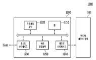
도 1은 반도체 메모리 장치(100)를 보여주는 블록도이다.FIG. 1 is a block diagram showing a
도 1을 참조하면, 반도체 메모리 장치(100)는 메모리 셀 어레이(110) 및 주변 회로(120)를 포함한다.Referring to FIG. 1, a
메모리 셀 어레이(110)는 행 라인들(RL)을 통해 어드레스 디코더(121)에 연결된다. 메모리 셀 어레이(110)는 비트 라인들(BL)을 통해 읽기 및 쓰기 회로(123)에 연결된다.The
메모리 셀 어레이(110)는 복수의 메모리 블록들을 포함한다. 복수의 메모리 블록들 각각은 복수의 셀 스트링들을 포함한다. 복수의 셀 스트링들 각각은 기판 위(over)에 적층되는 복수의 메모리 셀들을 포함한다. 실시 예로서, 복수의 메모리 셀들은 불휘발성 메모리 셀들이다. 실시 예로서, 복수의 메모리 셀들 각각은 싱글 레벨 셀(singl level cell) 또는 멀티 레벨 셀(multi level cells)로 정의될 수 있다. 메모리 셀 어레이(110)에 대해서 도 2 내지 도 4를 참조하여 더 상세히 설명된다.The
주변 회로(120)는 어드레스 디코더(121), 전압 발생기(122), 읽기 및 쓰기 회로(123), 입출력 버퍼(124) 및 제어 로직(125)을 포함한다.The
어드레스 디코더(121)은 제어 로직(125)의 제어에 응답하여 동작한다. 어드레스 디코더(121)은 행 라인들(RL)을 통해 메모리 셀 어레이(110)에 연결되고, 행 라인들(RL)을 제어하도록 구성된다. 여기에서 행 라인들(RL)은 드레인 선택 라인들, 워드 라인들, 소스 선택 라인들 및 공통 소스 라인을 포함한다. 실시 예로서, 행 라인들(RL)은 파이프 라인을 더 포함할 수 있다.The
어드레스 디코더(121)은 제어 로직(125)로부터 어드레스(ADDR)를 수신한다.The
프로그램 동작 및 읽기 동작 시에, 어드레스(ADDR)는 블록 어드레스 및 행 어드레스를 포함한다. 어드레스 디코더(121)은 수신된 어드레스(ADDR) 중 블록 어드레스를 디코딩하도록 구성된다. 어드레스 디코더(121)은 디코딩된 블록 어드레스에 따라 하나의 메모리 블록을 선택한다. 어드레스 디코더(121)은 수신된 어드레스(ADDR) 중 행 어드레스를 디코딩하도록 구성된다. 어드레스 디코더(121)은 디코딩된 행 어드레스에 따라 선택된 메모리 블록의 드레인 선택 라인들 중 어느 하나를 선택하고, 선택된 메모리 블록의 복수의 워드 라인들 중 어느 하나를 선택한다. 이에 따라, 하나의 페이지에 해당하는 메모리 셀들이 선택된다.In a program operation and a read operation, an address ADDR includes a block address and a row address. The
실시 예로서, 소거 동작 시에 어드레스(ADDR)는 블록 어드레스를 포함한다. 어드레스 디코더(121)은 블록 어드레스를 디코딩하고, 디코딩된 블록 어드레스에 따라 하나의 메모리 블록을 선택한다.As an example, in the erase operation, the address ADDR includes a block address. The
본 발명의 실시 예에 따르면, 반도체 메모리 장치(100)는 메모리 셀 어레이(110) 내 소스 선택 트랜지스터들을 프로그램한다. 이에 따라 소스 선택 트랜지스터들의 문턱 전압들이 원하는 전압 범위에 속할 수 있다. 소스 선택 트랜지스터들에 대한 프로그램은 각 페이지의 메모리 셀들에 대한 프로그램 이전에 수행될 수 있다. 소스 선택 트랜지스터들에 대한 프로그램 시에, 어드레스 디코더(121)는 제어 로직(125)의 제어에 응답하여 선택된 소스 선택 라인에 프로그램 전압을 제공할 것이다. 이때, 어드레스 디코더(121)는 공통 소스 라인을 기준 전압(예를 들면, 접지)으로 바이어스할 것이다.According to an embodiment of the present invention, the
실시 예로서, 어드레스 디코더(121)은 블록 디코더, 행 디코더 및 어드레스 버퍼 등을 포함할 수 있다.As an example, the
전압 발생기(122)는 제어 로직(125)의 제어에 응답하여 동작한다. 전압 발생기(122)는 반도체 메모리 장치(100)에 공급되는 외부 전원 전압을 이용하여 내부 전원 전압을 생성한다. 예를 들면, 전압 발생기(122)는 외부 전원 전압을 레귤레이팅하여 내부 전원 전압을 생성한다. 이렇게 생성된 내부 전원 전압은 어드레스 디코더(121), 읽기 및 쓰기 회로(123), 입출력 버퍼(124) 및 제어 로직(125)에 제공되어 반도체 메모리 장치(100)의 동작 전압으로서 사용된다.
전압 발생기(122)는 외부 전원 전압 및 내부 전원 전압 중 적어도 하나를 이용하여 복수의 전압들을 생성한다. 실시 예로서, 전압 발생기(122)는 내부 전원 전압을 수신하는 복수의 펌핑 커패시터들을 포함하고, 제어 로직(125)의 제어에 응답하여 복수의 펌핑 커패시터들을 선택적으로 활성화함으로써 복수의 전압들을 생성한다. 예를 들면, 전압 발생기(122)는 행 라인들(RL)에 인가되기 위한 다양한 전압들을 생성하고, 생성된 전압들을 어드레스 디코더(121)에 제공할 수 있다.The
읽기 및 쓰기 회로(123)은 비트 라인들(BL)을 통해 메모리 셀 어레이(110)에 연결된다. 읽기 및 쓰기 회로(123)은 제어 로직(125)의 제어에 응답하여 비트 라인들(BL)을 제어하도록 구성된다.The read and write
소거 동작 시에, 읽기 및 쓰기 회로(123)은 비트 라인들(BL)을 플로팅시킬 수 있다. 프로그램 동작 시에, 읽기 및 쓰기 회로(123)는 입출력 버퍼(124)로부터의 프로그램될 데이터(DATA)를 비트 라인들(BL)에 전달한다. 전달된 데이터(DATA)에 따라 선택된 메모리 셀들은 프로그램된다. 읽기 동작 시에, 읽기 및 쓰기 회로(123)는 비트 라인들(BL)을 통해 선택된 메모리 셀들로부터 비트 라인들(BL)을 통해 데이터(DATA)를 읽고, 읽어진 데이터(DATA)를 입출력 버퍼(124)로 출력한다.In an erase operation, the read and write
실시 예로서, 읽기 및 쓰기 회로(123)은 페이지 버퍼들(또는 페이지 레지스터들), 열 선택 회로 등을 포함할 수 있다.As an example, the read and write
제어 로직(125)는 어드레스 디코더(121), 전압 발생기(122), 읽기 및 쓰기 회로(123), 그리고 입출력 버퍼(124)에 연결된다. 제어 로직(125)는 입출력 버퍼(124)로부터 제어 신호(CTRL) 및 어드레스(ADDR)를 수신한다. 제어 로직(125)는 제어 신호(CTRL)에 응답하여 반도체 메모리 장치(100)의 제반 동작을 제어하도록 구성된다. 제어 로직(125)는 어드레스(ADDR)를 어드레스 디코더(121)에 전송한다.The
입출력 버퍼(124)는 외부로부터 제어 신호(CTRL) 및 어드레스(ADDR)를 수신하고, 수신된 제어 신호(CTRL) 및 어드레스(ADDR)를 제어 로직(125)에 전달한다. 또한, 입출력 버퍼는 외부로부터 입력된 데이터(DATA)를 읽기 및 쓰기 회로(123)에 전달하고, 또는 읽기 및 쓰기 회로(123)로부터 수신된 데이터(DATA)를 외부로 출력하도록 구성될 것이다.The input /
실시 예로서, 반도체 메모리 장치(100)는 플래시 메모리 장치(Flash Memory Device) 일 수 있다.As an embodiment, the
본 발명의 실시 예에 따르면, 반도체 메모리 장치(100)는 메모리 셀 어레이(110) 내 소스 선택 트랜지스터들을 프로그램한다. 소스 선택 트랜지스터들에 대한 프로그램 동작이 수행됨으로써, 소스 선택 트랜지스터들의 문턱 전압들은 원하는 전압 범위에 해당하게 된다. 이후 수행되는 메모리 셀들에 대한 프로그램 동작 또는 읽기 동작 시에, 소스 선택 트랜지스터들은 의도대로 제어될 것이다. 따라서, 반도체 메모리 장치(100)의 신뢰성은 향상된다.
According to an embodiment of the present invention, the
도 2는 도 1의 메모리 셀 어레이(110)의 일 실시 예를 보여주는 블록도이다.2 is a block diagram illustrating one embodiment of the
도 2를 참조하면, 메모리 셀 어레이(110)는 복수의 메모리 블록들(BLK1~BLKz)을 포함한다. 각 메모리 블록은 3차원 구조를 갖는다. 각 메모리 블록은 기판 위에 적층된 복수의 메모리 셀들을 포함한다. 이러한 복수의 메모리 셀들은 +X 방향, +Y 방향 및 +Z 방향을 따라 배열된다. 각 메모리 블록의 구조는 도 3 및 도 4를 참조하여 더 상세히 설명된다.
Referring to FIG. 2, the
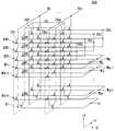
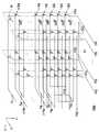
도 3은 도 2의 메모리 블록들(BLK1~BLKz) 중 어느 하나(BLK1)를 보여주는 회로도이다.FIG. 3 is a circuit diagram showing one of the memory blocks BLK1 to BLKz of FIG. 2 (BLK1).
도 3을 참조하면, 제 1 메모리 블록(BLK1)은 복수의 셀 스트링들(CS11~CS1m, CS21~CS2m)을 포함한다. 복수의 셀 스트링들(CS11~CS1m, CS21~CS2m) 각각은 'U'자형으로 형성될 수 있다. 제 1 메모리 블록(BLK1) 내에서, 행 방향(즉 +X 방향)으로 m개의 셀 스트링들이 배열된다. 도 3에서, 열 방향으로 2개의 셀 스트링들이 배열되는 것으로 도시된다. 하지만 이는 설명의 편의를 위한 것으로서 열 방향(즉 +Y)으로 2개 이상의 셀 스트링들이 배열될 수 있음이 이해될 것이다.Referring to FIG. 3, the first memory block BLK1 includes a plurality of cell strings CS11 to CS1m, CS21 to CS2m. Each of the plurality of cell strings CS11 to CS1m and CS21 to CS2m may be formed in a U shape. In the first memory block BLK1, m cell strings are arranged in the row direction (i.e., the + X direction). In Figure 3, two cell strings are shown arranged in the column direction. However, it will be understood that two or more cell strings may be arranged in the column direction (i.e., + Y) for convenience of explanation.
복수의 셀 스트링들(CS11~CS1m, CS21~CS2m) 각각은 적어도 하나의 소스 선택 트랜지스터(SST1~SST3), 제 1 내지 제 n 메모리 셀들(MC1~MCn), 파이프 트랜지스터(PT), 그리고 적어도 하나의 드레인 선택 트랜지스터(DST1~DST3)을 포함한다.Each of the plurality of cell strings CS11 to CS1m and CS21 to CS2m includes at least one source selection transistor SST1 to SST3, first to nth memory cells MC1 to MCn, a pipe transistor PT, And drain select transistors DST1 to DST3.
선택 트랜지스터들(SST1~SST3, DST1~DST3) 및 메모리 셀들(MC1~MCn) 각각은 유사한 구조를 가질 수 있다. 실시 예로서, 선택 트랜지스터들(SST1~SST3, DST1~DST3) 및 메모리 셀들(MC1~MCn) 각각은 채널층, 터널링 절연막, 전하 저장막 및 블로킹 절연막을 포함할 수 있다. 따라서 선택 트랜지스터들(SST1~SST3, DST1~DST3) 및 메모리 셀들(MC1~MCn) 각각은 그것의 전하 저장막에 트랩된 전자들의 수에 따라 가변하는 문턱 전압을 갖는다.Each of the select transistors SST1 to SST3, DST1 to DST3 and the memory cells MC1 to MCn may have a similar structure. In an embodiment, each of the select transistors SST1 to SST3, DST1 to DST3, and the memory cells MC1 to MCn may include a channel layer, a tunneling insulating layer, a charge storage layer, and a blocking insulating layer. Thus, each of the select transistors SST1 to SST3, DST1 to DST3, and memory cells MC1 to MCn has a threshold voltage that varies according to the number of electrons trapped in its charge storage film.
도 3에서, 각 셀 스트링(each cell string)에 3개의 소스 선택 트랜지스터들(SST1~SST3)이 제공되는 것으로 예시된다. 각 셀 스트링의 제 1 내지 제 3 소스 선택 트랜지스터들(SST1~SST3)은 공통 소스 라인(CSL)과 메모리 셀들(MC1~MCp) 사이에서 직렬로 연결된다. 셀 스트링들(CS11~CS1m, CS21~CS2m)의 제 1 소스 선택 트랜지스터들(SST1)의 소스는 공통 소스 라인(CSL)에 공통 연결된다.In FIG. 3, three source select transistors (SST1 to SST3) are illustrated as being provided in each cell string. The first to third source select transistors SST1 to SST3 of each cell string are connected in series between the common source line CSL and the memory cells MC1 to MCp. The sources of the first source selection transistors SST1 of the cell strings CS11 to CS1m and CS21 to CS2m are connected in common to the common source line CSL.
실시 예로서, 동일한 행(+X 방향)에 배열된 셀 스트링들의 소스 선택 트랜지스터들(SST1~SST3)은 행 방향으로 신장되는 소스 선택 라인에 연결된다. 제 1 행의 셀 스트링들(CS11~CS1m)의 소스 선택 트랜지스터들(SST1~SST3)은 제 1 소스 선택 라인(SSL1)에 연결된다. 제 2 행의 셀 스트링들(CS21~CS2m)의 소스 선택 트랜지스터들(SST1~SST3)은 제 2 소스 선택 라인(SSL2)에 연결된다.As an embodiment, the source selection transistors SST1 to SST3 of the cell strings arranged in the same row (+ X direction) are connected to the source selection line extended in the row direction. The source selection transistors SST1 to SST3 of the cell strings CS11 to CS1m in the first row are connected to the first source selection line SSL1. The source selection transistors SST1 to SST3 of the cell strings CS21 to CS2m of the second row are connected to the second source selection line SSL2.
다른 실시 예로서, 상이한 행에 배열된 셀 스트링들의 소스 선택 트랜지스터들(SST1~SST3)은 하나의 소스 선택 라인에 연결될 수 있다. 예를 들면, 도 3의 제 1 및 제 2 소스 선택 라인들(SSL1, SSL2)은 서로 연결되어 하나의 라인으로서 제공될 수 있다. 이 경우, 제 1 행 및 제 2 행의 셀 스트링들(CS11~CS1m, CS21~CS2m)의 소스 선택 트랜지스터들(SST1~SST3)은 하나의 소스 선택 라인에 의해 제어될 것이다.As another embodiment, the source select transistors SST1 to SST3 of the cell strings arranged in different rows may be connected to one source select line. For example, the first and second source selection lines SSL1 and SSL2 of FIG. 3 may be connected to each other and provided as one line. In this case, the source selection transistors SST1 to SST3 of the cell strings CS11 to CS1m, CS21 to CS2m of the first row and the second row will be controlled by one source selection line.
각 셀 스트링의 제 1 내지 제 n 메모리 셀들(MC1~MCn)은 소스 선택 트랜지스터들(SST1~SST3)과 드레인 선택 트랜지스터들(DST1~DST3) 사이에 연결된다. 제 1 내지 제 n 메모리 셀들(MC1~MCn)은 제 1 내지 제 p 메모리 셀들(MC1~MCp)과 제 p+1 내지 제 n 메모리 셀들(MCp+1~MCn)로 구분될 수 있다. 제 1 내지 제 p 메모리 셀들(MC1~MCp)과 제 p+1 내지 제 n 메모리 셀들(MCp+1~MCn)은 파이프 트랜지스터(PT)를 통해 연결된다.The first to nth memory cells MC1 to MCn of each cell string are connected between the source select transistors SST1 to SST3 and the drain select transistors DST1 to DST3. The first to nth memory cells MC1 to MCn may be divided into first to pth memory cells MC1 to MCp and p + 1 to nth memory cells MCp + 1 to MCn. The first to pth memory cells MC1 to MCp and the p + 1 to nth memory cells MCp + 1 to MCn are connected through a pipe transistor PT.
제 1 내지 제 p 메모리 셀들(MC1~MCp)은 +Z 방향과 역방향으로 순차적으로 배열되며, 소스 선택 트랜지스터들(SST1~SST3)과 파이프 트랜지스터(PT) 사이에서 직렬 연결된다. 제 p+1 내지 제 n 메모리 셀들(MCp+1~MCn)은 +Z 방향으로 순차적으로 배열되며, 파이프 트랜지스터(PT)와 드레인 선택 트랜지스터들(DST1~DST3) 사이에서 직렬 연결된다. 제 1 내지 제 n 메모리 셀들(MC1~MCn)의 게이트들은 각각 제 1 내지 제 n 워드 라인들(WL1~WLn)에 연결된다.The first to pth memory cells MC1 to MCp are sequentially arranged in the direction opposite to the + Z direction and are connected in series between the source selection transistors SST1 to SST3 and the pipe transistor PT. The p + 1 to nth memory cells MCp + 1 to MCn are sequentially arranged in the + Z direction and are connected in series between the pipe transistor PT and the drain select transistors DST1 to DST3. The gates of the first to nth memory cells MC1 to MCn are connected to the first to the nth word lines WL1 to WLn, respectively.
각 셀 스트링의 파이프 트랜지스터(PT)는 제 1 내지 제 p 메모리 셀들(MC1~MCp) 및 제 p+1 내지 제 n 메모리 셀들(MCp+1~MCn) 사이에 연결된다. 각 셀 스트링의 파이프 트랜지스터(PT)의 게이트는 파이프 라인(PL)에 연결된다.The pipe transistor PT of each cell string is connected between the first to pth memory cells MC1 to MCp and the p + 1 to nth memory cells MCp + 1 to MCn. The gates of the pipe transistors PT of each cell string are connected to the pipeline PL.
도 3에서, 각 셀 스트링에 3개의 드레인 선택 트랜지스터들(DST1~DST3)이 제공되는 것으로 예시된다. 각 셀 스트링의 제 1 내지 제 3 드레인 선택 트랜지스터들(DST1~DST3)은 해당 비트 라인과 메모리 셀들(MCp+1~MCn) 사이에 직렬 연결된다. 제 3 드레인 선택 트랜지스터(DST3)의 드레인은 해당 비트 라인에 연결된다.In Fig. 3, it is illustrated that three drain selection transistors DST1 to DST3 are provided for each cell string. The first to third drain selection transistors DST1 to DST3 of each cell string are connected in series between the corresponding bit line and the memory cells MCp + 1 to MCn. The drain of the third drain select transistor DST3 is connected to the corresponding bit line.
동일한 행(+X 방향)에 배열된 셀 스트링들의 드레인 선택 트랜지스터들(DST1~DST3)은 행 방향으로 신장되는 드레인 선택 라인에 연결된다. 제 1 및 제 2 드레인 선택 라인들(DSL1, DSL2)에 의해 각각 제 1 행 및 제 2 행이 정의된다. 제 1 행의 셀 스트링들(CS11~CS1m)의 드레인 선택 트랜지스터들(DST1~DST3)은 제 1 드레인 선택 라인(DSL1)에 연결된다. 제 2 행의 셀 스트링들(CS21~CS2m)의 드레인 선택 트랜지스터들(DST1~DST3)은 제 2 드레인 선택 라인(DSL2)에 연결된다.The drain selection transistors DST1 to DST3 of the cell strings arranged in the same row (+ X direction) are connected to a drain selection line extending in the row direction. The first row and the second row are defined by the first and second drain select lines DSL1 and DSL2, respectively. The drain selection transistors DST1 to DST3 of the cell strings CS11 to CS1m in the first row are connected to the first drain selection line DSL1. The drain selection transistors DST1 to DST3 of the cell strings CS21 to CS2m of the second row are connected to the second drain selection line DSL2.
실시 예로서, 각 셀 스트링의 제 1 내지 제 3 드레인 선택 트랜지스터들(DST1~DST3)은 도 3에 도시된 바와 같이 하나의 드레인 선택 라인에 연결될 수 있다. 도 3에 도시된 바와 상이하게, 각 셀 스트링의 제 1 내지 제 3 드레인 선택 트랜지스터들(DST1~DST3)은 상이한 드레인 선택 라인들에 연결될 수 있다.As an example, the first to third drain selection transistors DST1 to DST3 of each cell string may be connected to one drain selection line as shown in FIG. 3, the first to third drain select transistors DST1 to DST3 of each cell string may be connected to different drain select lines.
열(+Y 방향) 방향으로 배열되는 셀 스트링들은 열 방향으로 신장되는 비트 라인에 연결된다. 예를 들면, 제 1 열의 셀 스트링들(CS11, CS21)은 제 1 비트 라인(BL1)에 연결되어 있다. 제 m 열의 셀 스트링들(CS1m, CS2m)은 제 m 비트 라인(BLm)에 연결되어 있다.Cell strings arranged in the column (+ Y direction) direction are connected to bit lines extending in the column direction. For example, the cell strings CS11 and CS21 in the first column are connected to the first bit line BL1. The cell strings CS1m and CS2m in the m-th column are connected to the m-th bit line BLm.
각 셀 스트링에서, 메모리 셀들(MC1~MCp) 및 소스 선택 트랜지스터들(SST1~SST3)은 메모리 블록(BLK1) 하부의 기판(미도시)과 교차하는 방향, 즉 +Z 방향으로 순차적으로 적층된다. 각 셀 스트링에서, 메모리 셀들(MCp+1~MCn) 및 드레인 선택 트랜지스터들(DST1~DST3)은 +Z 방향으로 순차적으로 적층된다.In each cell string, the memory cells MC1 to MCp and the source select transistors SST1 to SST3 are sequentially stacked in the direction crossing the substrate (not shown) under the memory block BLK1, that is, in the + Z direction. In each cell string, the memory cells MCp + 1 to MCn and the drain selection transistors DST1 to DST3 are sequentially stacked in the + Z direction.
반도체 메모리 장치(100, 도 1 참조)는 소스 선택 트랜지스터들(SST1~SST3)을 제어함으로써 메모리 셀들(MC1~MCn)을 공통 소스 라인(CSL)과 전기적으로 연결하거나 전기적으로 차단한다. 만약 소스 선택 트랜지스터들(SST1~SST3)의 문턱 전압들이 원하는 전압 분포에서 벗어나는 경우, 소스 선택 트랜지스터들(SST1~SST3)은 효과적으로 제어될 수 없다.The semiconductor memory device 100 (see FIG. 1) electrically connects or electrically disconnects the memory cells MC1 to MCn with the common source line CSL by controlling the source selection transistors SST1 to SST3. If the threshold voltages of the source select transistors SST1 to SST3 deviate from the desired voltage distribution, the source select transistors SST1 to SST3 can not be controlled effectively.
소스 선택 트랜지스터들(SST1~SST3)이 원하는 전압 분포보다 높은 문턱 전압들을 가진다고 가정한다. 소스 선택 트랜지스터들(SST1~SST3)을 턴온시키면서 임의의 동작을 수행하는 경우, 소스 선택 트랜지스터들(SST1~SST3)을 통해 공통 소스 라인(CSL)으로 흐르는 전류는 의도치 않게 감소할 수 있다. 즉, 셀 스트링을 통해 공통 소스 라인(CSL)으로 흐르는 전류량이 낮아질 수 있다.It is assumed that the source selection transistors SST1 to SST3 have threshold voltages higher than the desired voltage distribution. When performing an arbitrary operation while turning on the source select transistors SST1 to SST3, the current flowing through the source select transistors SST1 to SST3 to the common source line CSL may be unexpectedly reduced. That is, the amount of current flowing to the common source line CSL through the cell string can be lowered.
소스 선택 트랜지스터들(SST1~SST3)이 원하는 문턱 전압보다 낮은 문턱 전압들을 가진다고 가정한다. 소스 선택 트랜지스터들(SST1~SST3)을 턴오프시키면서 임의의 동작을 수행하는 경우, 소스 선택 트랜지스터들(SST1~SST3)을 통해 공통 소스 라인(CSL)으로 의도치 않게 전류가 유출될 수 있다.It is assumed that the source select transistors SST1 to SST3 have threshold voltages lower than the desired threshold voltage. When performing an arbitrary operation while turning off the source select transistors SST1 to SST3, current may inadvertently flow out through the source select transistors SST1 to SST3 to the common source line CSL.
따라서, 소스 선택 트랜지스터들(SST1~SST3)의 문턱 전압들을 효과적으로 세팅하는 것은 반도체 메모리 장치(100)의 신뢰성 향상에 중요한 요소가 된다.
Therefore, effectively setting the threshold voltages of the source select transistors SST1 to SST3 is an important factor for improving the reliability of the
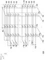
도 4는 도 2의 메모리 블록들(BLK1~BLKz) 중 어느 하나(BLK1)의 다른 실시 예(BLK1')를 보여주는 회로도이다.4 is a circuit diagram showing another embodiment (BLK1 ') of any one (BLK1) of the memory blocks BLK1 to BLKz of FIG.
도 4를 참조하면 제 1 메모리 블록(BLK1')은 복수의 셀 스트링들(CS11'~CS1m', CS21'~CS2m')을 포함한다. 복수의 셀 스트링들(CS11'~CS1m', CS21'~CS2m') 각각은 +Z 방향을 따라 신장된다. 복수의 셀 스트링들(CS11'~CS1m', CS21'~CS2m') 각각은, 메모리 블록(BLK1') 하부의 기판(미도시) 위에 적층된, 적어도 하나의 소스 선택 트랜지스터(SST1~SST3), 제 1 내지 제 n 메모리 셀들(MC1~MCn), 그리고 적어도 하나의 드레인 선택 트랜지스터(DST1~DST3)를 포함한다.Referring to FIG. 4, the first memory block BLK1 'includes a plurality of cell strings CS11' to CS1m ', CS21' to CS2m '. Each of the plurality of cell strings CS11 'to CS1m', CS21 'to CS2m' extend along the + Z direction. Each of the plurality of cell strings CS11 'to CS1m' and CS21 'to CS2m' includes at least one source selection transistor SST1 to SST3 stacked on a substrate (not shown) under the memory block BLK1 ' First to nth memory cells MC1 to MCn, and at least one drain select transistor DST1 to DST3.
각 셀 스트링의 제 1 내지 제 3 소스 선택 트랜지스터들(SST1~SST3)은 공통 소스 라인(CSL) 및 메모리 셀들(MC1~MCn) 사이에 직렬 연결된다. 각 셀 스트링의 제 1 소스 선택 트랜지스터(SST1)의 소스는 공통 소스 라인(CSL)에 연결된다.The first to third source select transistors SST1 to SST3 of each cell string are connected in series between the common source line CSL and the memory cells MC1 to MCn. The source of the first source select transistor SST1 of each cell string is connected to the common source line CSL.
동일한 행(+X 방향)에 배열된 셀 스트링들의 소스 선택 트랜지스터들(SST1~SST3)은 행 방향으로 신장되는 소스 선택 라인에 연결된다. 제 1 행의 셀 스트링들(CS11'~CS1m')의 소스 선택 트랜지스터들(SST1~SST3)은 제 1 소스 선택 라인(SSL1)에 연결된다. 제 2 행의 셀 스트링들(CS21'~CS2m')의 소스 선택 트랜지스터들(SST1~SST3)은 제 2 소스 선택 라인(SSL2)에 연결된다.The source selection transistors SST1 to SST3 of the cell strings arranged in the same row (+ X direction) are connected to a source selection line extending in the row direction. The source select transistors SST1 to SST3 of the cell strings CS11 'to CS1m' of the first row are connected to the first source select line SSL1. The source selection transistors SST1 to SST3 of the cell strings CS21 'to CS2m' of the second row are connected to the second source selection line SSL2.
각 셀 스트링의 제 1 내지 제 n 메모리 셀들(MC1~MCn)은 소스 선택 트랜지스터들(SST1~SST3)과 드레인 선택 트랜지스터들(DST1~DST3) 사이에서 직렬 연결된다. 제 1 내지 제 n 메모리 셀들(MC1~MCn)은 각각 제 1 내지 제 n 워드 라인들(WL1~WLn)에 연결된다.The first to nth memory cells MC1 to MCn of each cell string are connected in series between the source select transistors SST1 to SST3 and the drain select transistors DST1 to DST3. The first to nth memory cells MC1 to MCn are connected to the first to nth word lines WL1 to WLn, respectively.
각 셀 스트링의 제 1 내지 제 3 드레인 선택 트랜지스터들(DST1~DST3)은 해당 비트 라인과 메모리 셀들(MC1~MCn) 사이에 직렬 연결된다. 제 3 드레인 선택 트랜지스터(DST3)의 드레인은 해당 비트 라인에 연결된다.The first to third drain select transistors DST1 to DST3 of each cell string are serially connected between the corresponding bit line and the memory cells MC1 to MCn. The drain of the third drain select transistor DST3 is connected to the corresponding bit line.
동일한 행에 배열된 셀 스트링들의 드레인 선택 트랜지스터들(DST1~DST3)은 행 방향으로 신장되는 드레인 선택 라인에 연결된다. 제 1 행의 셀 스트링들(CS11'~CS1m')의 드레인 선택 트랜지스터들(DST1~DST3)은 제 1 드레인 선택 라인(DSL1)에 연결된다. 제 2 행의 셀 스트링들(CS21'~CS2m')의 드레인 선택 트랜지스터들(DST1~DST3)은 제 2 드레인 선택 라인(DSL2)에 연결된다.The drain selection transistors DST1 to DST3 of the cell strings arranged in the same row are connected to the drain selection line extended in the row direction. The drain selection transistors DST1 to DST3 of the cell strings CS11 'to CS1m' of the first row are connected to the first drain selection line DSL1. The drain selection transistors DST1 to DST3 of the cell strings CS21 'to CS2m' of the second row are connected to the second drain selection line DSL2.
결과적으로, 각 셀 스트링에 파이프 트랜지스터(PT)가 제외된 것을 제외하면 도 4의 메모리 블록(BLK1')은 도 3의 메모리 블록(BLK1)과 유사한 등가 회로를 갖는다.As a result, the memory block BLK1 'of FIG. 4 has an equivalent circuit similar to the memory block BLK1 of FIG. 3, except that the pipe transistor PT is excluded in each cell string.
이하, 설명의 편의를 위해 도 3의 메모리 블록(BLK1)을 중심으로 본 발명의 실시 예가 설명된다.
Hereinafter, for convenience of description, an embodiment of the present invention will be described centering on the memory block BLK1 of FIG.
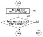
도 5는 본 발명의 실시 예에 따른 하나의 메모리 블록(BLK1)의 소스 선택 트랜지스터들(SST1~SST3)에 대한 프로그램 동작을 보여주는 순서도이다.5 is a flowchart showing the program operation for the source selection transistors SST1 to SST3 of one memory block BLK1 according to the embodiment of the present invention.
도 1, 도 3 및 도 5를 참조하면, S110단계에서, 소스 선택 라인들(SSL1, SSL2) 중 하나의 소스 선택 라인이 선택된다. 이하, 제 1 소스 선택 라인(SSL1)이 선택된다고 가정한다.1, 3 and 5, in step S110, a source selection line of one of the source selection lines SSL1 and SSL2 is selected. Hereinafter, it is assumed that the first source selection line SSL1 is selected.
S120단계에서, 선택된 소스 선택 라인(SSL1)과 연결된 소스 선택 트랜지스터들(SST1~SST3, 이하 선택된 소스 선택 트랜지스터들)에 대한 프로그램이 수행된다. 선택된 소스 선택 라인(SSL1)은 프로그램 전압으로 바이어스되고, 공통 소스 라인(CSL)은 기준 전압으로 바이어스된다. 예를 들면, 전압 발생기(122)는 제어 로직(125)의 제어에 응답하여 고 전압의 프로그램 전압을 생성할 것이다. 제어 로직(125)의 제어에 응답하여, 어드레스 디코더(121)는 전압 발생기(122)로부터의 프로그램 전압을 선택된 소스 선택 라인(SSL1)에 인가하고, 기준 전압을 공통 소스 라인(CSL)에 인가할 것이다.In step S120, a program for the source selection transistors SST1 to SST3 (hereinafter, selected source selection transistors) connected to the selected source selection line SSL1 is performed. The selected source select line SSL1 is biased to the program voltage, and the common source line CSL is biased to the reference voltage. For example, the
선택된 소스 선택 라인(SSL1)에 인가되는 프로그램 전압에 의해, 선택된 소스 선택 트랜지스터들(SST1~SST3)은 턴온되고, 그것들의 채널들에 공통 소스 라인(CSL)의 기준 전압이 전달될 것이다. 선택된 소스 선택 트랜지스터들(SST1~SST3)의 문턱 전압들은 공통 소스 라인(CSL)의 전압과 프로그램 전압의 차이에 의해 상승할 것이다.By the program voltage applied to the selected source selection line SSL1, the selected source selection transistors SST1 to SST3 are turned on and the reference voltage of the common source line CSL is transferred to the channels thereof. The threshold voltages of the selected source select transistors SST1 to SST3 will rise due to the difference between the voltage of the common source line CSL and the program voltage.
선택된 소스 선택 트랜지스터들(SST1~SST3)은 공통 소스 라인(CSL)에 직접적으로 연결된다. 비트 라인들(BL1~BLm)에 인가되는 전압들에 관계없이, 선택된 소스 선택 라인(SSL1)에 프로그램 전압이 인가될 때 선택된 소스 선택 트랜지스터들(SST1~SST3)의 채널들은 공통 소스 라인(CSL)의 전압을 수신할 것이다. 따라서 소스 선택 트랜지스터들(SST1~SST3)에 대한 프로그램은 비트 라인 단위로 제어되지는 않는다.The selected source select transistors SST1 to SST3 are directly connected to the common source line CSL. The channels of the source select transistors SST1 to SST3 selected when the program voltage is applied to the selected source select line SSL1 are applied to the common source line CSL regardless of the voltages applied to the bit lines BL1 to BLm, Lt; / RTI > Therefore, the program for the source select transistors SST1 to SST3 is not controlled on a bit line basis.
프로그램에 의해, 선택된 소스 선택 트랜지스터들(SST1~SST3)의 문턱 전압들은 상승할 것이다.By the program, the threshold voltages of the selected source select transistors SST1 to SST3 will rise.
S130단계에서, 선택된 소스 선택 트랜지스터들(SST1~SST3)에 대한 검증이 수행된다. 검증에 의해, 선택된 소스 선택 트랜지스터들(SST1~SST3)의 문턱 전압들이 판별된다.In step S130, verification of the selected source selection transistors SST1 to SST3 is performed. By the verification, the threshold voltages of the selected source select transistors SST1 to SST3 are discriminated.
실시 예로서, 선택된 소스 선택 트랜지스터들(SST1~SST3)의 문턱 전압들이 소정의 검증 전압보다 높은지 여부가 판별된다. 읽기 및 쓰기 회로(123)는 비트 라인들(BL1~BLm)에 소정의 전압 또는 전류를 제공하고, 어드레스 디코더(121)는 선택된 소스 선택 라인(SSL1)에 검증 전압(도 11의 Vvrf1 참조)을 인가할 것이다. 어드레스 디코더(121)는 행 라인들(DSL1, WL1~WLn, PL)을 제어하여 제 1 행의 셀 스트링들(CS11~CS1m)의 드레인 선택 트랜지스터들(DST1~DST3), 메모리 셀들(MC1~MCn) 및 파이프 트랜지스터들(PT)을 턴온시킬 것이다.As an embodiment, it is determined whether the threshold voltages of the selected source select transistors SST1 to SST3 are higher than a predetermined verify voltage. The read and write
비트 라인에 제공된 전압 또는 전류가 감소하는 것은, 해당 셀 스트링의 소스 선택 트랜지스터들(SST1~SST3)의 문턱 전압들이 검증 전압보다 낮다는 것을 의미할 수 있다. 비트 라인에 제공된 전압 또는 전류가 유지되는 것은, 해당 셀 스트링의 소스 선택 트랜지스터들(SST1~SST3)의 문턱 전압들 중 어느 하나가 목표 전압보다 높다는 것을 의미할 수 있다. 읽기 및 쓰기 회로(123)는 비트 라인 단위로 각 셀 스트링의 소스 선택 트랜지스터들(SST1~SST3)을 감지하고, 감지 결과를 제어 로직(125)에 전송할 것이다.The reduction in the voltage or current provided to the bit line may mean that the threshold voltages of the source select transistors SST1 to SST3 of the cell string are lower than the verify voltage. The voltage or current provided to the bit line may be maintained to indicate that any one of the threshold voltages of the source select transistors SST1 to SST3 of the corresponding cell string is higher than the target voltage. The read and write
선택된 소스 선택 트랜지스터들(SST1~SST3)의 문턱 전압들이 소정의 검증 전압보다 높은 것은 패스(pass)로 정의될 수 있다. 선택된 소스 선택 트랜지스터들(SST1~SST3) 중 정해진 개수(예를 들면 하나)가 소정의 검증 전압보다 낮은 문턱 전압을 갖는 것은 페일(fail)로 정의될 수 있다.The threshold voltages of the selected source select transistors SST1 to SST3 are higher than a predetermined verify voltage and can be defined as a pass. It can be defined that a predetermined number (for example, one) of the selected source select transistors SST1 to SST3 has a threshold voltage lower than a predetermined verify voltage as a fail.
S140단계에서, 제어 로직(125)은 검증 결과가 페일일 때, S150단계를 수행한다. 제어 로직(125)은 검증 결과가 패스일 때, S160단계를 수행한다.In step S140, the
S150단계에서, 프로그램 전압이 상승한다. 제어 로직(125)은 상승된 프로그램 전압을 발생하도록 전압 발생기(122)를 세팅할 것이다. 이후 상승된 프로그램 전압을 이용하여 S120단계가 재수행된다.In step S150, the program voltage rises.
S160단계에서, 선택된 소스 선택 라인(SSL1)이 마지막 소스 선택 라인일 때, 하나의 메모리 블록(BLK1)에 포함된 소스 선택 트랜지스터들(SST1~SST3)에 대한 프로그램 동작은 종료된다. 선택된 소스 선택 라인(SSL1)이 마지막 소스 선택 라인이 아닐 때, S110단계가 수행되어 다음 소스 선택 라인을 선택한다. 따라서 제 1 및 제 2 소스 선택 라인들(SSL1, SSL2) 각각에 대해 순차적으로 프로그램 동작이 수행될 것이다.
In step S160, when the selected source select line SSL1 is the last source select line, the program operation for the source select transistors SST1 to SST3 included in one memory block BLK1 is ended. When the selected source select line SSL1 is not the last source select line, step S110 is performed to select the next source select line. Therefore, the program operation will be sequentially performed for each of the first and second source selection lines SSL1 and SSL2.
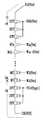
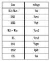
도 6은 도 5의 S120단계에서 인가되는 전압들의 일 실시 예를 보여주는 테이블이다. 도 7은 선택된 소스 선택 라인(SSL1)과 연결된 셀 스트링들(CS11~CS1m) 중 어느 하나(CS11)를 보여주는 회로도이다. 도 8은 비선택된 소스 선택 라인(SSL2)과 연결된 셀 스트링들(CS21~CS2m) 중 어느 하나(CS21)를 보여주는 회로도이다.FIG. 6 is a table showing an embodiment of the voltages applied in step S120 of FIG. FIG. 7 is a circuit diagram showing one of the cell strings CS11 to CS1m connected to the selected source selection line SSL1. 8 is a circuit diagram showing one of the cell strings CS21 to CS2m connected to the unselected source selection line SSL2.
도 3 및 도 6을 참조하면, 비트 라인들(BL1~BLm), 드레인 선택 라인들(DSL1, DSL2), 워드 라인들(WL1~WLn), 파이프 라인(PL) 및 공통 소스 라인(CSL)에 기준 전압(Vss, 예를 들면 접지 전압)이 인가된다. 메모리 블록(BLK1)에 포함된, 드레인 선택 트랜지스터들(DST1~DST3), 메모리 셀들(MC1~MCn) 및 파이프 트랜지스터들(PT)의 문턱 전압들은 유지될 것이다.3 and 6, the bit lines BL1 to BLm, the drain select lines DSL1 and DSL2, the word lines WL1 to WLn, the pipeline PL and the common source line CSL A reference voltage Vss (for example, a ground voltage) is applied. The threshold voltages of the drain selection transistors DST1 to DST3, the memory cells MC1 to MCn, and the pipe transistors PT included in the memory block BLK1 will be maintained.
선택된 소스 선택 라인(SSL1)에 고 전압의 프로그램 전압(Vpgm)이 인가된다. 프로그램 전압(Vpgm)이 인가됨에 따라, 선택된 소스 선택 라인(SSL1)에 연결된 소스 선택 트랜지스터들(SST1~SST3)에 채널들이 형성되고, 그러므로 선택된 소스 선택 트랜지스터들(SST1~SST3)은 턴온될 것이다. 형성된 채널들에 공통 소스 라인(CSL)의 기준 전압(Vss)이 전달될 것이다(도 7의 a). 그리고, 선택된 소스 선택 트랜지스터들(SST1~SST3)의 문턱 전압들은 선택된 소스 선택 라인(SSL1)의 프로그램 전압(Vpgm)과 해당 채널들의 기준 전압 사이의 차이에 의해 상승할 것이다.A program voltage Vpgm of a high voltage is applied to the selected source selection line SSL1. As the program voltage Vpgm is applied, channels are formed in the source select transistors SST1 to SST3 connected to the selected source select line SSL1, and thus the selected source select transistors SST1 to SST3 will be turned on. The reference voltage Vss of the common source line CSL will be transferred to the formed channels (Fig. 7A). The threshold voltages of the selected source selection transistors SST1 to SST3 will rise due to the difference between the program voltage Vpgm of the selected source selection line SSL1 and the reference voltage of the corresponding channels.
메모리 셀들(MC1~MCn) 및 드레인 선택 트랜지스터들(DST1~DST3)은 턴오프된다. 이에 따라, 공통 소스 라인(CSL)의 전압은, 메모리 셀들(MC1~MCn)의 채널들 및 드레인 선택 트랜지스터들(DST1~DST3)의 채널들에 전달되지 않는다(도 7의 b). 또한, 비트 라인(BL1)의 전압은, 드레인 선택 트랜지스터들(DST1~DST3)의 채널들 및 메모리 셀들(MC1~MCn)의 채널들에 전달되지 않는다(도 7의 c).The memory cells MC1 to MCn and the drain selection transistors DST1 to DST3 are turned off. Thus, the voltage of the common source line CSL is not transferred to the channels of the memory cells MC1 to MCn and the channels of the drain selection transistors DST1 to DST3 (Fig. 7B). Further, the voltage of the bit line BL1 is not transferred to the channels of the drain selection transistors DST1 to DST3 and the channels of the memory cells MC1 to MCn (FIG. 7C).
비선택된 소스 선택 라인(SSL2)에 프로그램 금지 전압(Vpih)이 인가된다. 프로그램 금지 전압(Vpih)은 저전압일 수 있다. 예를 들면, 프로그램 금지 전압(Vpih)은 기준 전압일 수 있다. 실시 예로서, 비선택된 소스 선택 라인(SSL2)과 연결된 소스 선택 트랜지스터들(SST1~SST3, 이하 비선택된 소스 선택 트랜지스터들)이 턴온되지 않도록, 프로그램 금지 전압(Vpih)이 설정될 수 있다. 그러므로, 공통 소스 라인(CSL)의 전압은 비선택된 소스 선택 트랜지스터들(SST1~SST3)에 전달되지 않는다(도 8의 d). 또한, 프로그램 금지 전압(Vpih)은 저전압이므로, 비선택된 소스 선택 트랜지스터들(SST1~SST3)의 문턱 전압들은 상승하지 않는다.The program inhibition voltage Vpih is applied to the non-selected source selection line SSL2. The program inhibition voltage Vpih may be a low voltage. For example, the program inhibition voltage Vpih may be a reference voltage. As an embodiment, the program inhibit voltage Vpih may be set such that the source select transistors SST1 to SST3 (hereinafter, unselected source select transistors) connected to the unselected source select line SSL2 are not turned on. Therefore, the voltage of the common source line CSL is not transferred to the unselected source select transistors SST1 to SST3 (Fig. 8 (d)). In addition, since the program inhibition voltage Vpih is a low voltage, the threshold voltages of the unselected source selection transistors SST1 to SST3 do not rise.
메모리 셀들(MC1~MCn) 및 드레인 선택 트랜지스터들(DST1~DST3)은 턴오프되므로, 비트 라인(BL1)의 전압은 드레인 선택 트랜지스터들(DST1~DST3)의 채널들 및 메모리 셀들(MC1~MCn)의 채널들에 전달되지 않는다(도 8의 e).Since the memory cells MC1 to MCn and the drain selection transistors DST1 to DST3 are turned off, the voltage of the bit line BL1 is lower than the voltage of the channels of the drain selection transistors DST1 to DST3 and the memory cells MC1 to MCn. Lt; / RTI > (e in FIG. 8).
다른 실시 예로서, 프로그램 금지 전압(Vpih)은 비선택된 소스 선택 트랜지스터들(SST1~SST3)을 턴온시키도록 설정될 수 있다. 이러한 경우 비선택된 소스 선택 트랜지스터들(SST1~SST3)에 채널들에 공통 소스 라인(CSL)의 기준 전압(Vss)이 전달될 것이다. 하지만, 프로그램 금지 전압(Vpih)과 공통 소스 라인(CSL)의 기준 전압(Vss)의 차이가 상대적으로 낮아 비선택된 소스 선택 트랜지스터들(SST1~SST3)의 문턱 전압들이 상승할 수 없도록, 프로그램 금지 전압(Vpih)이 설정될 수 있다.As another example, the program inhibition voltage Vpih may be set to turn on the unselected source select transistors SST1 to SST3. In this case, the reference voltage Vss of the common source line CSL will be transferred to the non-selected source select transistors SST1 to SST3. However, since the difference between the program inhibition voltage Vpih and the reference voltage Vss of the common source line CSL is relatively low so that the threshold voltages of the unselected source selection transistors SST1 to SST3 can not rise, (Vpih) can be set.
본 발명의 실시 예에 따르면, 프로그램 시에 선택된 소스 선택 트랜지스터들(SST1~SST3)의 채널들은 그것들에 직접적으로 연결된 공통 소스 라인(CSL)으로부터 전압을 수신한다. 선택된 소스 선택 라인(SSL1)의 프로그램 전압(Vpgm)과 공통 소스 라인(CSL)으로부터의 전압 사이의 차이에 의해, 선택된 소스 선택 트랜지스터들(SST1~SST3)은 프로그램된다. 드레인 선택 라인(DSL1) 및 워드 라인들(WL1~WLn)에 소정의 턴온 전압들이 인가되어 드레인 선택 트랜지스터들(DST1~DST3) 및 메모리 셀들(MC1~MCn)이 턴온되지 않더라도, 선택된 소스 선택 트랜지스터들(SST1~SST3)은 프로그램될 수 있다. 따라서 본 발명의 실시 예에 따르면, 선택된 소스 선택 트랜지스터들(SST1~SST3)에 대한 프로그램 시에, 메모리 셀들(MC1~MCn) 및 드레인 선택 트랜지스터들(DST1~DST3)에 높은 전압들이 인가되어 유발되는 디스터브는 감소할 것이다.
According to an embodiment of the present invention, the channels of the source select transistors SST1 to SST3 selected at the time of programming receive voltage from a common source line CSL directly connected to them. The selected source selection transistors SST1 to SST3 are programmed by the difference between the program voltage Vpgm of the selected source selection line SSL1 and the voltage from the common source line CSL. Even if the predetermined turn-on voltages are applied to the drain select line DSL1 and the word lines WL1 to WLn so that the drain select transistors DST1 to DST3 and the memory cells MC1 to MCn are not turned on, (SST1 to SST3) can be programmed. Therefore, according to the embodiment of the present invention, when programming the selected source selection transistors SST1 to SST3, high voltages are applied to the memory cells MC1 to MCn and the drain selection transistors DST1 to DST3 Disturb will decrease.
도 9는 도 5의 S120단계에서 인가되는 전압들의 다른 실시 예를 보여주는 테이블이다.FIG. 9 is a table showing another embodiment of the voltages applied in step S120 of FIG.
도 3 및 도 9를 참조하면, 비트 라인들(BL1~BLm), 드레인 선택 라인들(DSL1, DSL2), 워드 라인들(WL1~WLn) 및 파이프 라인(PL)이 플로팅된다. 비트 라인들(BL1~BLm), 드레인 선택 라인들(DSL1, DSL2), 워드 라인들(WL1~WLn) 및 파이프 라인(PL) 각각의 전압은 선택된 소스 선택 라인들(SSL1)의 프로그램 전압(Vpgm)과의 커플링(coupling) 효과에 의해 상승할 것이다. 따라서 비트 라인들(BL1~BLm), 드레인 선택 라인들(DSL1, DSL2), 워드 라인들(WL1~WLn) 및 파이프 라인(PL)과, 선택된 소스 선택 라인(SSL1) 사이의 전계(electric field)는 완화될 수 있다. 더불어, 비트 라인들(BL1~BLm), 드레인 선택 라인들(DSL1, DSL2), 워드 라인들(WL1~WLn) 및 파이프 라인(PL)을 바이어스하기 위한 전원이 소모되지 않을 것이다.Referring to FIGS. 3 and 9, bit lines BL1 to BLm, drain select lines DSL1 and DSL2, word lines WL1 to WLn, and a pipeline PL are plotted. The voltage of each of the bit lines BL1 to BLm, the drain select lines DSL1 and DSL2, the word lines WL1 to WLn and the pipeline PL is the program voltage Vpgm of the selected source select lines SSL1 ) Due to the coupling effect. The electric field between the bit lines BL1 to BLm, the drain select lines DSL1 and DSL2, the word lines WL1 to WLn and the pipeline PL and the selected source select line SSL1, Can be mitigated. In addition, the power for biasing the bit lines BL1 to BLm, the drain select lines DSL1 and DSL2, the word lines WL1 to WLn, and the pipeline PL will not be consumed.
선택된 소스 선택 라인(SSL1)에 고 전압의 프로그램 전압(Vpgm)이 인가된다. 공통 소스 라인(CSL)에 기준 전압(Vss)이 인가된다. 선택된 소스 선택 트랜지스터들(SST1~SST3)의 문턱 전압들은 상승할 것이다.A program voltage Vpgm of a high voltage is applied to the selected source selection line SSL1. And the reference voltage Vss is applied to the common source line CSL. The threshold voltages of the selected source select transistors SST1 to SST3 will rise.
실시 예로서, 비선택된 소스 선택 라인(SSL2)은 플로팅될 수 있다. 비선택된 소스 선택 라인(SSL2)은 선택된 소스 선택 라인들(SSL1)의 프로그램 전압(Vpgm)에 따라 상승할 것이다. 따라서 비선택된 소스 선택 라인(SSL2)과 선택된 소스 선택 라인들(SSL1) 사이의 전계는 완화될 수 있다.As an example, the unselected source select line SSL2 may be plotted. The unselected source select line SSL2 will rise in accordance with the program voltage Vpgm of the selected source select lines SSL1. Thus, the electric field between the unselected source select line SSL2 and the selected source select lines SSL1 can be relaxed.
한편, 비선택된 소스 선택 트랜지스터들(SST1~SST3)의 채널들 또한 선택된 소스 선택 라인들(SSL1)의 프로그램 전압(Vpgm)에 따라 상승할 것이다. 따라서 비선택된 소스 선택 라인(SSL2)의 상승된 전압과 비선택된 소스 선택 트랜지스터들(SST1~SST3)의 채널들의 상승된 전압들 사이의 차이는 낮을 것이다. 결과적으로, 비선택된 소스 선택 트랜지스터들(SST1~SST3)의 문턱 전압들은 상승하지 않는다.
On the other hand, the channels of the unselected source select transistors SST1 to SST3 will also rise in accordance with the program voltage Vpgm of the selected source select lines SSL1. The difference between the raised voltage of the unselected source select line SSL2 and the raised voltages of the channels of the unselected source select transistors SST1 to SST3 will be low. As a result, the threshold voltages of the unselected source select transistors SST1 to SST3 do not rise.
도 10은 도 5의 S120단계에서 인가되는 전압들의 또 다른 실시 예를 보여주는 테이블이다.FIG. 10 is a table showing another embodiment of the voltages applied in step S120 of FIG.
도 3 및 도 10을 참조하면, 비트 라인들(BL1~BLm)에 기준 전압(Vss)이 인가된다. 선택된 드레인 선택 라인(DSL1), 워드 라인들(WL1~WLn) 및 파이프 라인(PL)에 제 1 및 제 2 턴온 전압들(Vtrn1, Vtrn2)이 인가된다. 제 1 및 제 2 턴온 전압들(Vtrn1, Vtrn2)은 선택된 드레인 선택 라인(DSL1)과 연결된 드레인 선택 트랜지스터들(DST1~DST3), 해당 메모리 셀들(MC1~MCn) 및 해당 파이프 트랜지스터들(PT)을 턴온시키기 위한 전압들일 것이다. 제 2 턴온 전압(Vtrn2)은 제 1 턴온 전압(Vtrn1)보다 높을 수 있다. 제 1 및 제 2 턴온 전압들(Vtrn1, Vtrn2)은 프로그램 전압(Vpgm)보다 낮다. 이에 따라, 비트 라인들(BL1~BLm)의 기준 전압(Vss)이 선택된 소스 선택 트랜지스터들(SST1~SST3)의 채널들로 전달될 수 있다.Referring to FIGS. 3 and 10, the reference voltage Vss is applied to the bit lines BL1 to BLm. The first and second turn-on voltages Vtrn1 and Vtrn2 are applied to the selected drain select line DSL1, the word lines WL1 to WLn, and the pipeline PL. The first and second turn-on voltages Vtrn1 and Vtrn2 are applied to the drain select transistors DST1 to DST3 connected to the selected drain select line DSL1, the memory cells MC1 to MCn and the corresponding pipe transistors PT It will be the voltages to turn on. The second turn-on voltage Vtrn2 may be higher than the first turn-on voltage Vtrn1. The first and second turn-on voltages Vtrn1 and Vtrn2 are lower than the program voltage Vpgm. Accordingly, the reference voltage Vss of the bit lines BL1 to BLm can be transferred to the channels of the selected source select transistors SST1 to SST3.
비선택된 드레인 선택 라인(DSL2)에 턴오프 전압(Vtrf)이 인가될 수 있다. 턴오프 전압(Vtrf)은 비선택된 드레인 선택 라인(DSL2)과 연결된 드레인 선택 트랜지스터들(DST1~DST3)을 턴오프시키기 위한 전압일 것이다. 이에 따라, 비트 라인들(BL1~BLm)의 기준 전압(Vss)은 비선택된 소스 선택 트랜지스터들(SST1~SST3)에 전달되지 않는다.The turn-off voltage Vtrf may be applied to the unselected drain select line DSL2. The turn-off voltage Vtrf may be a voltage for turning off the drain select transistors DST1 to DST3 connected to the unselected drain select line DSL2. Accordingly, the reference voltage Vss of the bit lines BL1 to BLm is not transmitted to the unselected source selection transistors SST1 to SST3.
도 4를 참조한 메모리 블록(BLK1')에 이 실시 예를 적용하면, 선택된 드레인 선택 라인(DSL1), 워드 라인들(WL1~WLn) 및 파이프 라인(PL)에 인가되는 전압들(Vtrn1, Vtrn2)은 해당 라인이 선택된 소스 선택 라인(SSL1)에 인접할수록 높아진다. 따라서 선택된 드레인 선택 라인(DSL1), 워드 라인들(WL1~WLn) 및 파이프 라인(PL)과, 선택된 소스 선택 라인(SSL1) 사이의 전계는 완화될 수 있다.Applying this embodiment to the memory block BLK1 'with reference to FIG. 4 results in the voltages Vtrn1 and Vtrn2 applied to the selected drain select line DSL1, word lines WL1 to WLn and the pipeline PL, Becomes higher as the line is adjacent to the selected source selection line (SSL1). The electric field between the selected drain select line DSL1, the word lines WL1 to WLn and the pipeline PL and the selected source select line SSL1 can be relaxed.
선택된 소스 선택 라인(SSL1)에 고 전압의 프로그램 전압(Vpgm)이 인가된다. 공통 소스 라인(CSL)에 기준 전압(Vss)이 인가된다. 선택된 소스 선택 라인(SSL1)과 연결된 소스 선택 트랜지스터들(SST1~SST3)의 채널들은, 비트 라인들(BL1~BLm) 및 공통 소스 라인(CSL)으로부터 기준 전압(Vss)을 수신할 수 있다. 프로그램 전압(Vpgm)과 기준 전압(Vss)의 차이에 따라 선택된 소스 선택 트랜지스터들(SST1~SST3)의 문턱 전압들은 상승할 것이다.A program voltage Vpgm of a high voltage is applied to the selected source selection line SSL1. And the reference voltage Vss is applied to the common source line CSL. The channels of the source select transistors SST1 to SST3 connected to the selected source select line SSL1 can receive the reference voltage Vss from the bit lines BL1 to BLm and the common source line CSL. The threshold voltages of the source selection transistors SST1 to SST3 selected in accordance with the difference between the program voltage Vpgm and the reference voltage Vss will rise.
비선택된 소스 선택 라인(SSL2)에 프로그램 금지 전압(Vpih)이 인가된다. 프로그램 금지 전압(Vpih)은 저전압이므로, 비선택된 소스 선택 트랜지스터들(SST1~SST3)의 문턱 전압들은 상승하지 않는다.
The program inhibition voltage Vpih is applied to the non-selected source selection line SSL2. Since the program inhibition voltage Vpih is a low voltage, the threshold voltages of the unselected source selection transistors SST1 to SST3 do not rise.
도 11은 선택된 소스 선택 트랜지스터들(SST1~SST3)에 대한 프로그램 동작 시에 선택된 소스 선택 트랜지스터들(SST1~SST3)의 문턱 전압 산포의 일 예를 보여주는 도면이다. 도 12는 도 5의 S130단계 및 S140단계의 일 실시 예를 보여주는 도면이다.11 is a diagram showing an example of the threshold voltage distribution of the source selection transistors SST1 to SST3 selected during the program operation for the selected source selection transistors SST1 to SST3. 12 is a view showing one embodiment of steps S130 and S140 of FIG.
도 3 및 도 11을 참조하면, 프로그램 동작 전에, 선택된 소스 선택 트랜지스터들(SST1~SST3)은 제 1 문턱 전압 상태(TVD11)를 갖는다. 이후 선택된 소스 선택 트랜지스터들(SST1~SST3)에 대한 프로그램이 수행되면, 선택된 소스 선택 트랜지스터들(SST1~SST3)의 문턱 전압들은 상승하여 제 2 문턱 전압 상태(TVD12)를 갖는다.Referring to FIGS. 3 and 11, before the program operation, the selected source select transistors SST1 to SST3 have a first threshold voltage state TVD11. Then, when the program for the selected source select transistors SST1 to SST3 is performed, the threshold voltages of the selected source select transistors SST1 to SST3 rise to have a second threshold voltage state TVD12.
실시 예로서, 선택된 소스 선택 트랜지스터들(SST1~SST3)에 대한 검증 시에, 선택된 소스 선택 트랜지스터들(SST1~SST3)의 문턱 전압들이 제 1 검증 전압(Vvrf1)보다 높은지 여부가 판별될 수 있다. 도 12를 참조하면, 제 1 검증 전압(Vvrf1)을 이용하여 선택된 소스 선택 트랜지스터들(SST1~SST3)을 읽는다(S210). 선택된 소스 선택 라인(SSL1)에 제 1 검증 전압(Vvrf1)이 인가될 것이다. 선택된 드레인 선택 라인(DSL1), 워드 라인들(WL1~WLn) 및 파이프 라인(PL)이 제어되어 해당 드레인 선택 트랜지스터들(DST1~DST3), 해당 메모리 셀들(MC1~MCn) 및 해당 파이프 트랜지스터들(PT)이 턴온될 것이다. 비트 라인들(BL1~BLm)을 통해 선택된 소스 선택 트랜지스터들(SST1~SST3)이 읽혀질 것이다.As an embodiment, it can be determined whether the threshold voltages of the selected source select transistors SST1 to SST3 are higher than the first verify voltage Vvrf1 during the verification of the selected source select transistors SST1 to SST3. Referring to FIG. 12, the selected source selection transistors SST1 to SST3 are read using the first verify voltage Vvrf1 (S210). The first verify voltage Vvrf1 will be applied to the selected source select line SSL1. The selected drain select line DSL1, the word lines WL1 to WLn and the pipeline PL are controlled so that the corresponding drain select transistors DST1 to DST3, the corresponding memory cells MC1 to MCn, PT) will be turned on. The source select transistors SST1 to SST3 selected through the bit lines BL1 to BLm will be read.
선택된 소스 선택 트랜지스터들(SST1~SST3)의 문턱 전압들이 제 1 검증 전압(Vvrf1)보다 높을 때, S160단계가 수행될 것이다(S220). 선택된 소스 선택 트랜지스터들(SST1~SST3) 중 적어도 하나가 제 1 검증 전압(Vvrf1)보다 낮을 때, S150단계가 수행될 것이다(S220). 도 11에서, 제 2 문턱 전압 상태(TVD12)는 제 1 검증 전압(Vvrf1)보다 낮다. 따라서 S150단계가 수행되고, 상승된 프로그램 전압을 이용하여 선택된 소스 선택 트랜지스터들(SST1~SST3)이 재프로그램될 것이다.When the threshold voltages of the selected source select transistors SST1 to SST3 are higher than the first verify voltage Vvrf1, step S160 will be performed (S220). When at least one of the selected source select transistors SST1 to SST3 is lower than the first verify voltage Vvrf1, step S150 will be performed (S220). 11, the second threshold voltage state TVD12 is lower than the first verify voltage Vvrf1. Thus, step S150 is performed, and the selected source select transistors SST1 to SST3 will be reprogrammed using the elevated program voltage.
이러한 방식으로 선택된 소스 선택 트랜지스터들(SST1~SST3)에 대한 프로그램이 반복되면, 선택된 소스 선택 트랜지스터들(SST1~SST3)의 문턱 전압들은 제 3 문턱 전압 상태(TVD13)를 거쳐 제 4 문턱 전압 상태(TVD14)에 도달할 것이다.When the program for the selected source selection transistors SST1 to SST3 is repeated in this manner, the threshold voltages of the selected source selection transistors SST1 to SST3 are changed to the fourth threshold voltage state (TVD13) via the third threshold voltage state TVD13 TVD14).
제 4 문턱 전압 상태(TVD14)의 전압 범위는 제 1 검증 전압(Vvrf1)보다 높다. 예를 들면, 선택된 소스 선택 라인(SSL1)에 제 1 검증 전압(Vvrf1)이 인가되어 비트 라인들(BL1~BLm)을 통해 선택된 소스 선택 트랜지스터들(SST1~SST3)이 읽혀질 때, 선택된 소스 선택 트랜지스터들(SST1~SST3)은 오프 셀들로 판별될 것이다. 선택된 소스 선택 트랜지스터들(SST1~SST3)에 대한 프로그램 동작은 종료될 것이다.The voltage range of the fourth threshold voltage state TVD14 is higher than the first verification voltage Vvrf1. For example, when the first verify voltage Vvrf1 is applied to the selected source select line SSL1 and the selected source select transistors SST1 to SST3 are read through the bit lines BL1 to BLm, (SST1 to SST3) will be determined as off-cells. The program operation for the selected source select transistors SST1 to SST3 will be terminated.
결과적으로, 선택된 소스 선택 트랜지스터들(SST1~SST3)은 제 1 검증 전압(Vvrf1)보다 높은 문턱 전압들을 갖는다. 이 실시 예에 따르면, 선택된 소스 선택 트랜지스터들(SST1~SST3)의 턴오프 특성을 효율적으로 세팅할 수 있다.
As a result, the selected source select transistors SST1 to SST3 have threshold voltages higher than the first verify voltage Vvrf1. According to this embodiment, the turn-off characteristics of the selected source select transistors SST1 to SST3 can be set efficiently.
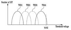
도 13는 선택된 소스 선택 트랜지스터들(SST1~SST3)에 대한 프로그램 동작 시에 선택된 소스 선택 트랜지스터들(SST1~SST3)의 문턱 전압 산포의 다른 예를 보여주는 도면이다. 도 14는 도 5의 S130단계 및 S140단계의 일 실시 예를 보여주는 도면이다.13 is a diagram showing another example of the threshold voltage distribution of the source selection transistors SST1 to SST3 selected in the program operation for the selected source selection transistors SST1 to SST3. FIG. 14 is a view showing one embodiment of steps S130 and S140 of FIG.
도 13을 참조하면, 프로그램 동작 전에, 선택된 소스 선택 트랜지스터들(SST1~SST3)은 제 1 문턱 전압 상태(TVD11)를 갖는다. 이후 선택된 소스 선택 트랜지스터들(SST1~SST3)에 대한 프로그램이 수행되면, 선택된 소스 선택 트랜지스터들(SST1~SST3)의 문턱 전압들은 상승하여 제 5 문턱 전압 상태(TVD21)를 갖는다.Referring to FIG. 13, before the program operation, the selected source selection transistors SST1 to SST3 have a first threshold voltage state TVD11. Then, when a program for the selected source select transistors SST1 to SST3 is performed, the threshold voltages of the selected source select transistors SST1 to SST3 rise to have a fifth threshold voltage state TVD21.
실시 예로서, 선택된 소스 선택 트랜지스터들(SST1~SST3)에 대한 검증 시에, 선택된 소스 선택 트랜지스터들(SST1~SST3) 중 적어도 하나의 문턱 전압이 제 2 검증 전압(Vvrf2)보다 높은지 여부가 판별될 수 있다. 도 14를 참조하면, 제 2 검증 전압(Vvrf2)을 이용하여 선택된 소스 선택 트랜지스터들(SST1~SST3)을 읽는다(S310). 선택된 소스 선택 라인(SSL1)에 제 2 검증 전압(Vvrf2)이 인가되고, 비트 라인들(BL1~BLm)을 통해 선택된 소스 선택 트랜지스터들(SST1~SST3)이 읽혀질 것이다.As an embodiment, at the time of verification of the selected source selection transistors SST1 to SST3, it is determined whether or not the threshold voltage of at least one of the selected source selection transistors SST1 to SST3 is higher than the second verification voltage Vvrf2 . Referring to FIG. 14, the selected source selection transistors SST1 to SST3 are read using the second verify voltage Vvrf2 (S310). The second verify voltage Vvrf2 is applied to the selected source select line SSL1 and the selected source select transistors SST1 to SST3 are read through the bit lines BL1 to BLm.
선택된 소스 선택 트랜지스터들(SST1~SST3) 중 적어도 하나의 문턱 전압이 제 2 검증 전압(Vvrf2)보다 높을 때, S160단계가 수행된다(S320). 선택된 소스 선택 트랜지스터들(SST1~SST3)의 문턱 전압들이 제 2 검증 전압(Vvrf2)보다 낮을 때 S150단계가 수행된다(S320). 도 13에서, 제 5 문턱 전압 상태(TVD21)는 제 2 검증 전압(Vvrf2)보다 낮다. 따라서 S150단계가 수행되고, 상승된 프로그램 전압을 이용하여 선택된 소스 선택 트랜지스터들(SST1~SST3)이 재프로그램될 것이다.When at least one threshold voltage of the selected source select transistors SST1 to SST3 is higher than the second verify voltage Vvrf2, step S160 is performed (S320). When the threshold voltages of the selected source select transistors SST1 to SST3 are lower than the second verify voltage Vvrf2, step S150 is performed (S320). 13, the fifth threshold voltage state TVD21 is lower than the second verify voltage Vvrf2. Thus, step S150 is performed, and the selected source select transistors SST1 to SST3 will be reprogrammed using the elevated program voltage.
이러한 방식으로 선택된 소스 선택 트랜지스터들(SST1~SST3)에 대한 프로그램이 반복되면, 선택된 소스 선택 트랜지스터들(SST1~SST3)의 문턱 전압들은 제 6 문턱 전압 상태(TVD31)를 거쳐 제 7 문턱 전압 상태(TVD41)에 도달할 것이다.When the program for the selected source select transistors SST1 to SST3 is repeated in this way, the threshold voltages of the selected source select transistors SST1 to SST3 are changed to the seventh threshold voltage state (TVD31) through the sixth threshold voltage state TVD31 TVD41).
제 7 문턱 전압 상태(TVD41)의 전압 범위 중 가장 높은 전압은 제 2 검증 전압(Vvrf2)보다 높다. 즉, 검증 시에, 선택된 소스 선택 트랜지스터들(SST1~SST3) 중 적어도 하나는 제 2 검증 전압(Vvrf2)보다 높다. 선택된 소스 선택 트랜지스터들(SST1~SST3)에 대한 프로그램 동작은 종료될 것이다.The highest voltage among the voltage range of the seventh threshold voltage state TVD41 is higher than the second verification voltage Vvrf2. That is, at the time of verification, at least one of the selected source select transistors SST1 to SST3 is higher than the second verify voltage Vvrf2. The program operation for the selected source select transistors SST1 to SST3 will be terminated.
결과적으로, 선택된 소스 선택 트랜지스터들(SST1~SST3)의 대부분이 임의의 전압과 제 2 검증 전압(Vvrf2) 사이의 문턱 전압들을 갖게 된다. 이 실시 예에 따르면, 선택된 소스 선택 트랜지스터들(SST1~SST3)의 문턱 전압들이 과도하게 상승하지 않는다. 선택된 소스 선택 트랜지스터들(SST1~SST3)이 전류를 통과시키는 특성을 효율적으로 세팅할 수 있다.
As a result, most of the selected source selection transistors SST1 to SST3 have threshold voltages between the arbitrary voltage and the second verify voltage Vvrf2. According to this embodiment, the threshold voltages of the selected source select transistors SST1 to SST3 do not rise excessively. It is possible to efficiently set the characteristic that the selected source select transistors SST1 to SST3 pass the current.
도 15는 도 2의 메모리 블록들(BLK1~BLKz) 중 어느 하나(BLK1)의 또 다른 실시 예(BLK11)를 보여주는 회로도이다.FIG. 15 is a circuit diagram showing another embodiment (BLK11) of any one (BLK1) of the memory blocks BLK1 to BLKz of FIG.
도 15를 참조하면, 메모리 블록(BLK11)은 이븐 셀 스트링들(CSe11~CSe1p) 오드 셀 스트링들(CSo11~CSo1p)을 포함한다.Referring to FIG. 15, the memory block BLK11 includes even cell strings CSe11 to CSe1p and od cell strings CSo11 to CSo1p.
이븐 셀 스트링들(CSe11~CSe1p) 및 오드 셀 스트링들(CSo11~CSo1p) 각각은 적어도 하나의 소스 선택 트랜지스터(SST1~SST3), 제 1 내지 제 n 메모리 셀들(MC1~MCn), 파이프 트랜지스터(PT), 그리고 적어도 하나의 드레인 선택 트랜지스터(DST1~DST3)를 포함한다.Each of the even cell strings CSe11 to CSe1p and od cell strings CSo11 to CSo1p includes at least one source select transistor SST1 to SST3, first to nth memory cells MC1 to MCn, a pipe transistor PT ), And at least one drain select transistor (DST1 to DST3).
도 15의 이븐 셀 스트링들(CSe11~CSe1p) 및 오드 셀 스트링들(CSo11~CSo1p)은 도 3의 제 1 행의 셀 스트링들(CS11~CS1m)의 변형 실시 예로서 이해될 수 있다.The even cell strings CSe11 to CSe1p and odd cell strings CSo11 to CSo1p in Fig. 15 can be understood as modified embodiments of the cell strings CS11 to CS1m in the first row in Fig.
제 1 내지 제 p 이븐 셀 스트링들(CSe11~CSe1p)은 각각 제 1 내지 제 p 이븐 비트 라인들(BLe1~BLep)에 연결된다. 제 1 내지 제 p 오드 셀 스트링들(CSo11~CSo1p)은 각각 제 1 내지 제 p 오드 비트 라인들(BLo1~BLop)에 연결된다. 이븐 셀 스트링들(CSe11~CSe1p) 및 오드 셀 스트링들(CSo11~CSo1p)은 공통 소스 라인(CSL)에 공통 연결된다.The first to p-th cell strings CSe11 to CSe1p are connected to the first to p-th bit lines BLe1 to BLep, respectively. The first to pth odd cell strings CSo11 to CSo1p are connected to the first to pth odd bit lines BLo1 to BLop, respectively. The even cell strings CSe11 to CSe1p and odd cell strings CSo11 to CSo1p are connected in common to the common source line CSL.
각 셀 스트링의 제 1 내지 제 n 메모리 셀들(MC1~MCn)은 제 1 내지 제 n 워드 라인들(WL1~WLn)에 연결된다.The first to nth memory cells MC1 to MCn of each cell string are connected to the first to nth word lines WL1 to WLn.
제 1 내지 제 p 이븐 셀 스트링들(CSe11~CSe1p)의 드레인 선택 트랜지스터들(DST1~DST3)은 제 1 이븐 드레인 선택 라인(DSLe1)에 연결된다. 제 1 내지 제 p 오드 셀 스트링들(CSo11~CSo1p)의 드레인 선택 트랜지스터들(DST1~DST3)은 제 1 오드 드레인 선택 라인(DSLo1)에 연결된다.The drain select transistors DST1 to DST3 of the first to p-th cell strings CSe11 to CSe1p are connected to the first even drain select line DSLe1. The drain selection transistors DST1 to DST3 of the first to pseudo cell strings CSo11 to CSo1p are connected to the first odd-numbered drain selection line DSLo1.
이븐 셀 스트링들(CSe11~CSe1p) 및 오드 셀 스트링들(CSo11~CSo1p)의 소스 선택 트랜지스터들(SST1~SST3)은 하나의 소스 선택 라인(SSL1)에 연결된다.The source selection transistors SST1 to SST3 of the even cell strings CSe11 to CSe1p and the od cell strings CSo11 to CSo1p are connected to one source selection line SSL1.
결과적으로, 이븐 셀 스트링과 오드 셀 스트링은 상이한 드레인 선택 라인들(DSLe1, DSLo1)에 연결되고, 동일한 소스 선택 라인(SSL1)에 연결된다.As a result, the even cell string and the od cell string are connected to different drain select lines DSLe1 and DSLo1, and are connected to the same source select line SSL1.
도 15의 이븐 셀 스트링들(CSe11~CSe1p) 및 오드 셀 스트링들(CSo11~CSo1p)을 하나의 셀 스트링 그룹으로 정의할 때, 열 방향(즉 +Y 방향)으로 배열되어 이븐 비트 라인들(BLe1~BLep) 및 오드 비트 라인들(BLo1~BLop)에 연결되는 다른 셀 스트링 그룹이 메모리 블록(BLK11)에 더 포함될 수 있음이 이해될 것이다.
When the odd cell strings CSe11 to CSe1p and the odd cell strings CSo11 to CSo1p of FIG. 15 are defined as one cell string group, they are arranged in the column direction (i.e., the + Y direction) ~ BLep and another cell string group connected to the odd bit lines BLo1 ~ BLop may be further included in the memory block BLK11.
도 16은 도 2의 메모리 블록들(BLK1~BLKz) 중 어느 하나(BLK1)의 다른 실시 예(BLK22)를 보여주는 회로도이다.Fig. 16 is a circuit diagram showing another embodiment (BLK22) of any one of the memory blocks BLK1 to BLKz of Fig. 2 (BLK1).
도 16을 참조하면, 메모리 블록(BLK22)은 이븐 셀 스트링들(CSe11'~CSe1p') 오드 셀 스트링들(CSo11'~CSo1p')을 포함한다.Referring to FIG. 16, the memory block BLK22 includes od cell strings CSe11 'to CSe1p' and od cell strings CSo11 'to CSo1p'.
이븐 셀 스트링들(CSe11'~CSe1p') 및 오드 셀 스트링들(CSo11'~CSo1p') 각각은 적어도 하나의 소스 선택 트랜지스터(SST1~SST3), 제 1 내지 제 n 메모리 셀들(MC1~MCn), 그리고 적어도 하나의 드레인 선택 트랜지스터(DST1~DST3)를 포함한다.Each of the odd cell strings CSe11'-CSe1p 'and odd cell strings CSo11'-CSo1p'includes at least one of the source select transistors SST1 to SST3, the first to n'th memory cells MC1 to MCn, And at least one drain select transistor (DST1 to DST3).
도 16의 이븐 셀 스트링들(CSe11'~CSe1p') 및 오드 셀 스트링들(CSo11'~CSo1p')은 도 4의 제 1 행의 셀 스트링들(CS11'~CS1m')의 변형 실시 예로서 이해될 수 있다.The even cell strings CSe11 'to CSe1p' and odd cell strings CSo11 'to CSo1p' in FIG. 16 are understood as modified embodiments of the cell strings CS11 'to CS1m' in the first row of FIG. .
제 1 내지 제 p 이븐 셀 스트링들(CSe11'~CSe1p')은 각각 제 1 내지 제 p 이븐 비트 라인들(BLe1~BLep)에 연결된다. 제 1 내지 제 p 오드 셀 스트링들(CSo11'~CSo1p')은 각각 제 1 내지 제 p 오드 비트 라인들(BLo1~BLop)에 연결된다. 이븐 셀 스트링들(CSe11'~CSe1p') 및 오드 셀 스트링들(CSo11'~CSo1p')은 공통 소스 라인(CSL)에 공통 연결된다.The first to p-th cell strings CSe11 'to CSe1p' are connected to the first to p'th bit lines BLe1 to BLep, respectively. The first to pth odd cell strings CSo11 'to CSo1p' are connected to the first to pth odd bit lines BLo1 to BLop, respectively. The even cell strings CSe11 'to CSe1p' and odd cell strings CSo11 'to CSo1p' are connected in common to the common source line CSL.
각 셀 스트링의 제 1 내지 제 n 메모리 셀들(MC1~MCn)은 제 1 내지 제 n 워드 라인들(WL1~WLn)에 연결된다.The first to nth memory cells MC1 to MCn of each cell string are connected to the first to nth word lines WL1 to WLn.
제 1 내지 제 p 이븐 셀 스트링들(CSe11'~CSe1p')의 드레인 선택 트랜지스터들(DST1~DST3)은 제 1 이븐 드레인 선택 라인(DSLe1)에 연결된다. 제 1 내지 제 p 오드 셀 스트링들(CSo11'~CSo1p')의 드레인 선택 트랜지스터들(DST1~DST3)은 제 1 오드 드레인 선택 라인(DSLo1)에 연결된다.The drain select transistors DST1 to DST3 of the first to p-th cell strings CSe11 'to CSe1p' are connected to the first even drain select line DSLe1. The drain selection transistors DST1 to DST3 of the first to pseudo cell strings CSo11 'to CSo1p' are connected to the first odd-numbered drain selection line DSLo1.
이븐 셀 스트링들(CSe11'~CSe1p') 및 오드 셀 스트링들(CSo11'~CSo1p')의 소스 선택 트랜지스터들(SST1~SST3)은 하나의 소스 선택 라인(SSL1)에 연결된다.The source select transistors SST1 to SST3 of the even cell strings CSe11'-CSe1p 'and od cell strings CSo11' to CSo1p 'are connected to one source select line SSL1.
결과적으로, 이븐 셀 스트링과 오드 셀 스트링은 상이한 드레인 선택 라인들(DSLe1, DSLo1)에 연결되고, 동일한 소스 선택 라인(SSL1)에 연결된다.As a result, the even cell string and the od cell string are connected to different drain select lines DSLe1 and DSLo1, and are connected to the same source select line SSL1.
각 셀 스트링에서 파이프 트랜지스터(PT)가 제외된 것을 제외하면, 도 16의 메모리 블록(BLK22)은 도 15의 메모리 블록(BLK11)과 유사한 등가 회로를 갖는다.The memory block BLK22 of Fig. 16 has an equivalent circuit similar to the memory block BLK11 of Fig. 15, except that the pipe transistor PT is excluded in each cell string.
이하, 설명의 편의를 위해 도 15의 메모리 블록(BLK11)을 중심으로 본 발명의 실시 예가 설명된다.
Hereinafter, for convenience of description, an embodiment of the present invention will be described with reference to the memory block BLK11 of Fig.
도 17은 이븐 셀 스트링들(CSe11~CSe1p) 및 오드 셀 스트링들(CSo11~CSo1p)의 소스 선택 트랜지스터들(SST1~SST3)에 대한 프로그램 동작을 보여주는 순서도이다.17 is a flowchart showing the program operation for the source selection transistors SST1 to SST3 of the odd cell strings CSo11 to CSo1p and odd cell strings CSe11 to CSe1p.
도 15 및 도 17을 참조하면, S410단계에서, 소스 선택 라인(SSL1)이 선택된다. S420단계 내지 S460단계에서, 선택된 소스 선택 라인(SSL1)과 연결된 셀 스트링 그룹의 소스 선택 트랜지스터들(SST1~SST3)에 대한 프로그램 동작이 수행된다.15 and 17, in step S410, a source selection line SSL1 is selected. In steps S420 to S460, a program operation is performed on the source selection transistors SST1 to SST3 of the cell string group connected to the selected source selection line SSL1.
먼저 S420단계에서, 선택된 소스 선택 트랜지스터들(SST1~SST3)에 대한 프로그램이 수행된다. 선택된 소스 선택 라인(SSL1)은 프로그램 전압으로 바이어스되고, 공통 소스 라인(CSL)은 기준 전압으로 바이어스된다. 선택된 소스 선택 라인(SSL1)은 이븐 셀 스트링들(CSe11~CSe1p) 및 오드 셀 스트링들(CSo11~CSo1p)에 연결된다. 셀 스트링들(CSe11~CSe1p, CSo11~CSo1p)에 포함된 소스 선택 트랜지스터들(SST1~SST3)의 문턱 전압들은 상승할 것이다.First, in step S420, a program for the selected source selection transistors SST1 to SST3 is performed. The selected source select line SSL1 is biased to the program voltage, and the common source line CSL is biased to the reference voltage. The selected source selection line SSL1 is connected to odd cell strings CSe11 to CSe1p and odd cell strings CSo11 to CSo1p. The threshold voltages of the source selection transistors SST1 to SST3 included in the cell strings CSe11 to CSe1p and CSo11 to CSo1p will rise.
S430단계 내지 S460단계에서, 선택된 소스 선택 트랜지스터들(SST1~SST3)에 대한 검증이 수행된다.In steps S430 to S460, verification of the selected source selection transistors SST1 to SST3 is performed.
S430단계에서, 선택된 소스 선택 트랜지스터들(SST1~SST3) 중 이븐 셀 스트링들(CSe11~CSe1p)에 포함되는 소스 선택 트랜지스터들(SST1~SST3)에 대한 검증이 수행된다.In step S430, verification of the source selection transistors SST1 to SST3 included in the even cell strings CSe11 to CSe1p in the selected source selection transistors SST1 to SST3 is performed.
선택된 소스 선택 라인(SSL1)에 검증 전압이 인가될 것이다. 이때, 이븐 비트 라인들(BLe1~BLep)에 소정의 전압 또는 전류가 제공되고, 워드 라인들(WL1~WLn) 및 파이프 라인(PL)에 메모리 셀들(MC1~MCn) 및 파이프 트랜지스터들(PT)를 턴온시키기 위한 전압이 인가될 것이다.The verify voltage will be applied to the selected source select line SSL1. At this time, a predetermined voltage or current is supplied to the even bit lines BLe1 to BLep and the memory cells MC1 to MCn and the pipe transistors PT are connected to the word lines WL1 to WLn and the pipeline PL, A voltage for turning on the power supply will be applied.
이븐 드레인 선택 라인(DSLe1)은 이븐 셀 스트링들(CSe11~CSe1p)의 드레인 선택 트랜지스터들(DST1~DST3)을 턴온시키기 위한 전압을 수신할 것이다. 오드 드레인 선택 라인(DSLo1)은 오드 셀 스트링들(CSo11~CSo1p)의 드레인 선택 트랜지스터들(DST1~DST3)을 턴오프시키도록 바이어스될 것이다.The even drain select line DSLe1 will receive a voltage to turn on the drain select transistors DST1 to DST3 of the even cell strings CSe11 to CSe1p. The odd drain selection line DSLo1 will be biased to turn off the drain selection transistors DST1 to DST3 of the od cell strings CSo11 to CSo1p.
이븐 비트 라인들(BLe1~BLep)에 제공된 전압 또는 전류가 감소하는지 여부에 따라, 이븐 셀 스트링들(CSe11~CSe1p)에 포함되는 소스 선택 트랜지스터들(SST1~SST3)의 문턱 전압들이 읽어질 수 있다.The threshold voltages of the source select transistors SST1 to SST3 included in the even cell strings CSe11 to CSe1p can be read depending on whether the voltage or current supplied to the even bit lines BLe1 to BLep is decreasing .
S440단계에서, 검증 결과가 페일인 경우 S470단계가 수행된다. 프로그램 시 상승된 프로그램 전압이 생성되도록 전압 발생기(122)가 세팅될 것이다. 검증 결과가 패스인 경우 S450단계가 수행된다.In step S440, if the verification result is fail, step S470 is performed. The
S450단계에서, 선택된 소스 선택 트랜지스터들(SST1~SST3) 중 오드 셀 스트링들(CSo11~CSo1p)에 포함되는 소스 선택 트랜지스터들(SST1~SST3)에 대한 검증이 수행된다.In step S450, verification of the source selection transistors SST1 to SST3 included in the odd cell strings CSo11 to CSo1p among the selected source selection transistors SST1 to SST3 is performed.
선택된 소스 선택 라인(SSL1)에 검증 전압이 인가될 것이다. 이때, 오드 비트 라인들(BLo1~BLop)에 소정의 전압 또는 전류가 제공되고, 워드 라인들(WL1~WLn) 및 파이프 라인(PL)에 메모리 셀들(MC1~MCn) 및 파이프 트랜지스터들(PT)을 턴온시키기 위한 전압이 인가될 것이다. 오드 드레인 선택 라인(DSLo1)은 오드 셀 스트링들(CSo11~CSo1p)에 포함되는 드레인 선택 트랜지스터들(DST1~DST3)을 턴온시키기 위한 전압으로 바이어스될 것이다. 이븐 드레인 선택 라인(DSLe1)은 이븐 셀 스트링들(CSe11~CSe1p)에 포함되는 드레인 선택 트랜지스터들(DST1~DST3)을 턴오프시키기 위한 전압으로 바이어스될 것이다. 오드 비트 라인들(BLo1~BLop)에 제공된 전압 또는 전류가 감소하는지 여부에 따라, 오드 셀 스트링들(CSo11~CSo1p)에 포함되는 소스 선택 트랜지스터들(SST1~SST3)의 문턱 전압들이 읽어질 수 있다.The verify voltage will be applied to the selected source select line SSL1. At this time, a predetermined voltage or current is supplied to the odd bit lines BLo1 to BLop and the memory cells MC1 to MCn and the pipe transistors PT are connected to the word lines WL1 to WLn and the pipeline PL, A voltage for turning on the power supply will be applied. The odd drain selection line DSLo1 will be biased to a voltage for turning on the drain selection transistors DST1 to DST3 included in the od cell strings CSo11 to CSo1p. The even drain select line DSLe1 will be biased to a voltage for turning off the drain select transistors DST1 to DST3 included in the even cell strings CSe11 to CSe1p. The threshold voltages of the source select transistors SST1 to SST3 included in the od cell strings CSo11 to CSo1p can be read depending on whether the voltage or current supplied to the odd bit lines BLo1 to BLop is decreasing .
S460단계에서, 검증 결과가 페일인 경우 S470단계가 수행된다. 검증 결과가 패스인 경우 S480단계가 수행된다. 결과적으로 S480단계는 이븐 셀 스트링들(CSe11~CSe1p)의 소스 선택 트랜지스터들(SST1~SST3)에 대한 검증 및 오드 셀 스트링들(CSo11~CSo1p)의 소스 선택 트랜지스터들(SST1~SST3)에 대한 검증이 모두 패스될 때 수행된다.In step S460, if the verification result is fail, step S470 is performed. If the verification result is the path, step S480 is performed. As a result, in step S480, the verification of the source selection transistors SST1 to SST3 of the even cell strings CSe11 to CSe1p and the verification of the source selection transistors SST1 to SST3 of the odd cell strings CSo11 to CSo1p Are all passed.
S480단계에서, 선택된 소스 선택 라인(SSL1)이 마지막 소스 선택 라인인지 여부에 따라 다음 소스 선택 라인이 선택되거나(S410) 프로그램 동작이 종료된다.
In step S480, the next source selection line is selected (S410) depending on whether the selected source selection line SSL1 is the last source selection line or the program operation is terminated.
도 18은 도 1의 반도체 메모리 장치(100)를 포함하는 메모리 시스템(1000)을 보여주는 블록도이다.18 is a block diagram showing a
도 18을 참조하면, 메모리 시스템(1000)은 반도체 메모리 장치(100) 및 컨트롤러(1200)를 포함한다.18, the
반도체 메모리 장치(100)는 도 1을 참조하여 설명된 바와 마찬가지로 구성되고, 동작할 수 있다. 이하, 중복되는 설명은 생략된다.The
컨트롤러(1200)는 호스트(Host) 및 반도체 메모리 장치(100)에 연결된다. 호스트(Host)로부터의 요청에 응답하여, 컨트롤러(1200)는 반도체 메모리 장치(100)를 액세스하도록 구성된다. 예를 들면, 컨트롤러(1200)는 반도체 메모리 장치(100)의 읽기, 쓰기, 소거, 그리고 배경(background) 동작을 제어하도록 구성된다. 컨트롤러(1200)는 반도체 메모리 장치(100) 및 호스트(Host) 사이에 인터페이스를 제공하도록 구성된다. 컨트롤러(1200)는 반도체 메모리 장치(100)를 제어하기 위한 펌웨어(firmware)를 구동하도록 구성된다.The
컨트롤러(1200)는 램(1210, Random Access Memory), 프로세싱 유닛(1220, processing unit), 호스트 인터페이스(1230, host interface), 메모리 인터페이스(1240, memory interface) 및 에러 정정 블록(1250)을 포함한다.The
램(1210)은 프로세싱 유닛(1220)의 동작 메모리, 반도체 메모리 장치(100) 및 호스트(Host) 사이의 캐시 메모리, 그리고 반도체 메모리 장치(100) 및 호스트(Host) 사이의 버퍼 메모리 중 적어도 하나로서 이용된다.The
프로세싱 유닛(1220)은 컨트롤러(1200)의 제반 동작을 제어한다.The
호스트 인터페이스(1230)는 호스트(Host) 및 컨트롤러(1200) 사이의 데이터 교환을 수행하기 위한 프로토콜을 포함한다. 예시적인 실시 예로서, 컨트롤러(1200)는 USB (Universal Serial Bus) 프로토콜, MMC (multimedia card) 프로토콜, PCI (peripheral component interconnection) 프로토콜, PCI-E (PCI-express) 프로토콜, ATA (Advanced Technology Attachment) 프로토콜, Serial-ATA 프로토콜, Parallel-ATA 프로토콜, SCSI (small computer small interface) 프로토콜, ESDI (enhanced small disk interface) 프로토콜, 그리고 IDE (Integrated Drive Electronics) 프로토콜, 사유(private) 프로토콜 등과 같은 다양한 인터페이스 프로토콜들 중 적어도 하나를 통해 호스트(Host)와 통신하도록 구성된다.The
메모리 인터페이스(1240)는 반도체 메모리 장치(100)와 인터페이싱한다. 예를 들면, 메모리 인터페이스는 낸드 인터페이스 또는 노어 인터페이스를 포함한다.The
에러 정정 블록(1250)은 에러 정정 코드(ECC, Error Correcting Code)를 이용하여 반도체 메모리 장치(100)로부터 수신된 데이터의 에러를 검출하고, 정정하도록 구성된다.The
도 1을 참조하여 설명된 반도체 메모리 장치(100)가 제공됨으로써, 향상된 신뢰성을 갖는 메모리 시스템(1000)이 제공된다.By providing the
컨트롤러(1200) 및 반도체 메모리 장치(100)는 하나의 반도체 장치로 집적될 수 있다. 예시적인 실시 예로서, 컨트롤러(1200) 및 반도체 메모리 장치(100)는 하나의 반도체 장치로 집적되어, 메모리 카드를 구성할 수 있다. 예를 들면, 컨트롤러(1200) 및 반도체 메모리 장치(100)는 하나의 반도체 장치로 집적되어 PC 카드(PCMCIA, personal computer memory card international association), 컴팩트 플래시 카드(CF), 스마트 미디어 카드(SM, SMC), 메모리 스틱, 멀티미디어 카드(MMC, RS-MMC, MMCmicro), SD 카드(SD, miniSD, microSD, SDHC), 유니버설 플래시 기억장치(UFS) 등과 같은 메모리 카드를 구성할 것이다.The
컨트롤러(1200) 및 반도체 메모리 장치(100)는 하나의 반도체 장치로 집적되어 반도체 드라이브(SSD, Solid State Drive)를 구성할 수 있다. 반도체 드라이브(SSD)는 반도체 메모리에 데이터를 저장하도록 구성되는 저장 장치를 포함한다. 메모리 시스템(1000)이 반도체 드라이브(SSD)로 이용되는 경우, 메모리 시스템(1000)에 연결된 호스트(Host)의 동작 속도는 획기적으로 개선된다.The
다른 예로서, 메모리 시스템(1000)은 컴퓨터, UMPC (Ultra Mobile PC), 워크스테이션, 넷북(net-book), PDA (Personal Digital Assistants), 포터블(portable) 컴퓨터, 웹 타블렛(web tablet), 무선 전화기(wireless phone), 모바일 폰(mobile phone), 스마트폰(smart phone), e-북(e-book), PMP(portable multimedia player), 휴대용 게임기, 네비게이션(navigation) 장치, 블랙박스(black box), 디지털 카메라(digital camera), 3차원 수상기(3-dimensional television), 디지털 음성 녹음기(digital audio recorder), 디지털 음성 재생기(digital audio player), 디지털 영상 녹화기(digital picture recorder), 디지털 영상 재생기(digital picture player), 디지털 동영상 녹화기(digital video recorder), 디지털 동영상 재생기(digital video player), 정보를 무선 환경에서 송수신할 수 있는 장치, 홈 네트워크를 구성하는 다양한 전자 장치들 중 하나, 컴퓨터 네트워크를 구성하는 다양한 전자 장치들 중 하나, 텔레매틱스 네트워크를 구성하는 다양한 전자 장치들 중 하나, RFID 장치, 또는 컴퓨팅 시스템을 구성하는 다양한 구성 요소들 중 하나 등과 같은 전자 장치의 다양한 구성 요소들 중 하나로 제공된다.As another example, the
예시적인 실시 예로서, 반도체 메모리 장치(100) 또는 메모리 시스템(1000)은 다양한 형태들의 패키지로 실장될 수 있다. 예를 들면, 반도체 메모리 장치(100) 또는 메모리 시스템(1000)은 PoP(Package on Package), Ball grid arrays(BGAs), Chip scale packages(CSPs), Plastic Leaded Chip Carrier(PLCC), Plastic Dual In Line Package(PDIP), Die in Waffle Pack, Die in Wafer Form, Chip On Board(COB), Ceramic Dual In Line Package(CERDIP), Plastic Metric Quad Flat Pack(MQFP), Thin Quad Flatpack(TQFP), Small Outline integrated circuit (SOIC), Shrink Small Outline Package(SSOP), Thin Small Outline Package(TSOP), Thin Quad Flatpack(TQFP), System In Package(SIP), Multi Chip Package(MCP), Wafer-level Fabricated Package(WFP), Wafer-Level Processed Stack Package(WSP) 등과 같은 방식으로 패키지화되어 실장될 수 있다.
As an exemplary embodiment,
도 19는 도 18의 메모리 시스템(1000)의 응용 예(2000)를 보여주는 블록도이다.19 is a block diagram illustrating an
도 19를 참조하면, 메모리 시스템(2000)은 반도체 메모리 장치(2100) 및 컨트롤러(2200)를 포함한다. 반도체 메모리 장치(2100)는 복수의 반도체 메모리 칩들을 포함한다. 복수의 반도체 메모리 칩들은 복수의 그룹들로 분할된다.19, the
도 19에서, 복수의 그룹들은 각각 제 1 내지 제 k 채널들(CH1~CHk)을 통해 컨트롤러(2200)와 통신하는 것으로 도시되어 있다. 각 반도체 메모리 칩은 도 1을 참조하여 설명된 반도체 메모리 장치(100) 중 하나와 마찬가지로 구성되고, 동작할 것이다.In Fig. 19, a plurality of groups are shown as communicating with the
각 그룹은 하나의 공통 채널을 통해 컨트롤러(2200)와 통신하도록 구성된다. 컨트롤러(2200)는 도 18을 참조하여 설명된 컨트롤러(1200)와 마찬가지로 구성되고, 복수의 채널들(CH1~CHk)을 통해 반도체 메모리 장치(2100)의 복수의 메모리 칩들을 제어하도록 구성된다.Each group is configured to communicate with the
도 19에서, 하나의 채널에 복수의 반도체 메모리 칩들이 연결되는 것으로 설명되었다. 그러나, 하나의 채널에 하나의 반도체 메모리 칩이 연결되도록 메모리 시스템(2000)이 변형될 수 있음이 이해될 것이다.
In FIG. 19, it has been described that a plurality of semiconductor memory chips are connected to one channel. However, it will be appreciated that the
도 20은 도 19를 참조하여 설명된 메모리 시스템(2000)을 포함하는 컴퓨팅 시스템(3000)을 보여주는 블록도이다.20 is a block diagram illustrating a
도 20을 참조하면, 컴퓨팅 시스템(3000)은 중앙 처리 장치(3100), 램(3200, RAM, Random Access Memory), 사용자 인터페이스(3300), 전원(3400), 시스템 버스(3500), 그리고 메모리 시스템(2000)을 포함한다.20, a
메모리 시스템(2000)은 시스템 버스(3500)를 통해, 중앙처리장치(3100), 램(3200), 사용자 인터페이스(3300), 그리고 전원(3400)에 전기적으로 연결된다. 사용자 인터페이스(3300)를 통해 제공되거나, 중앙 처리 장치(3100)에 의해서 처리된 데이터는 메모리 시스템(2000)에 저장된다.The
도 20에서, 반도체 메모리 장치(2100)는 컨트롤러(2200)를 통해 시스템 버스(3500)에 연결되는 것으로 도시되어 있다. 그러나, 반도체 메모리 장치(2100)는 시스템 버스(3500)에 직접 연결되도록 구성될 수 있다. 이때, 컨트롤러(2200)의 기능은 중앙 처리 장치(3100) 및 램(3200)에 의해 수행될 것이다.In FIG. 20,
도 20에서, 도 19를 참조하여 설명된 메모리 시스템(2000)이 제공되는 것으로 도시되어 있다. 그러나, 메모리 시스템(2000)은 도 18을 참조하여 설명된 메모리 시스템(1000)으로 대체될 수 있다. 실시 예로서, 컴퓨팅 시스템(3000)은 도 18 및 도 19를 참조하여 설명된 메모리 시스템들(1000, 2000)을 모두 포함하도록 구성될 수 있다.In Fig. 20, it is shown that the
본 발명의 실시 예에 따르면, 반도체 메모리 장치는 메모리 셀 어레이 내 소스 선택 트랜지스터들을 프로그램한다. 소스 선택 트랜지스터들에 대한 프로그램 동작이 수행됨으로써, 소스 선택 트랜지스터들의 문턱 전압들은 원하는 전압 범위에 해당하게 된다. 따라서, 반도체 메모리 장치의 신뢰성은 향상된다.
According to an embodiment of the present invention, a semiconductor memory device programs source select transistors in a memory cell array. By performing a program operation on the source select transistors, the threshold voltages of the source select transistors correspond to the desired voltage range. Therefore, the reliability of the semiconductor memory device is improved.
본 발명의 상세한 설명에서는 구체적인 실시 예에 관하여 설명하였으나, 본 발명의 범위와 기술적 사상에서 벗어나지 않는 한도 내에서 다양한 변경이 가능하다. 그러므로 본 발명의 범위는 상술한 실시 예에 국한되어 정해져서는 안되며 후술하는 특허청구범위뿐만 아니라 이 발명의 특허청구범위와 균등한 것들에 의해 정해져야 한다.While the invention has been shown and described with reference to certain preferred embodiments thereof, it will be understood by those skilled in the art that various changes and modifications may be made without departing from the spirit and scope of the invention. Therefore, the scope of the present invention should not be limited to the above-described embodiments, but should be determined by the equivalents of the claims of the present invention as well as the claims of the following.
100: 반도체 메모리 장치
110: 메모리 셀 어레이
BLK1~BLKz: 제 1 내지 제 z 메모리 블록들
120: 주변 회로
121: 어드레스 디코더
122: 전압 발생기
123: 읽기 및 쓰기 회로
124: 입출력 버퍼
125: 제어 로직
SST1~SST3: 제 1 내지 제 3 소스 선택 트랜지스터들100: semiconductor memory device
110: memory cell array
BLK1 to BLKz: first to z < th > memory blocks
120: peripheral circuit
121:
122: voltage generator
123: Read and Write Circuit
124: I / O buffer
125: control logic
SST1 to SST3: First to third source select transistors
Claims (20)
Translated fromKorean상기 복수의 셀 스트링들의 소스 선택 트랜지스터들과 연결된 적어도 하나의 소스 선택 라인; 및
상기 복수의 셀 스트링들을 제어하도록 구성되는 주변 회로를 포함하되,
상기 주변 회로는 상기 적어도 하나의 소스 선택 라인 중 선택된 소스 선택 라인에 프로그램 전압을 인가하고 상기 공통 소스 라인에 기준 전압을 인가하여, 상기 선택된 소스 선택 라인과 연결된 소스 선택 트랜지스터들에 대한 프로그램을 수행하는 반도체 메모리 장치.A plurality of cell strings each including at least one source select transistor connected to a common source line and a plurality of memory cells connected to the common source line through the at least one source select transistor;
At least one source select line coupled to the source select transistors of the plurality of cell strings; And
And peripheral circuits configured to control the plurality of cell strings,
Wherein the peripheral circuitry performs a program for source select transistors coupled to the selected source select line by applying a programming voltage to a selected source select line of the at least one source select line and applying a reference voltage to the common source line Semiconductor memory device.
상기 주변 회로는 상기 적어도 하나의 소스 선택 라인 중 비선택된 소스 선택 라인에 상기 프로그램 전압보다 낮은 프로그램 금지 전압을 인가하여 상기 비선택된 소스 선택 라인과 연결된 소스 선택 트랜지스터들에 대한 프로그램을 금지하는 반도체 메모리 장치.The method according to claim 1,
Wherein the peripheral circuitry applies a program inhibit voltage lower than the program voltage to a non-selected source select line of the at least one source select line to inhibit programming for source select transistors coupled to the non- .
상기 주변 회로는 상기 적어도 하나의 소스 선택 라인 중 비선택된 소스 선택 라인을 플로팅하여 상기 비선택된 소스 선택 라인과 연결된 소스 선택 트랜지스터들에 대한 프로그램을 금지하는 반도체 메모리 장치.The method according to claim 1,
Wherein the peripheral circuitry floats the unselected source select line of the at least one source select line to inhibit programming for the source select transistors coupled to the unselected source select line.
상기 복수의 셀 스트링들 각각은 해당 비트 라인과 상기 복수의 메모리 셀들 사이에 연결된 적어도 하나의 드레인 선택 트랜지스터를 포함하고,
상기 복수의 셀 스트링들의 드레인 선택 트랜지스터들은 복수의 드레인 선택 라인들에 연결되고
상기 복수의 셀 스트링들의 메모리 셀들은 복수의 워드 라인들에 연결되는 반도체 메모리 장치.The method according to claim 1,
Each of the plurality of cell strings including at least one drain select transistor coupled between the bit line and the plurality of memory cells,
The drain select transistors of the plurality of cell strings are connected to a plurality of drain select lines
And the memory cells of the plurality of cell strings are connected to a plurality of word lines.
상기 프로그램 시에, 상기 주변 회로는 상기 복수의 셀 스트링들의 비트 라인들, 상기 복수의 드레인 선택 라인들 및 상기 복수의 워드 라인들에 상기 기준 전압을 인가하는 반도체 메모리 장치.5. The method of claim 4,
Wherein the peripheral circuit applies the reference voltage to the bit lines, the plurality of drain select lines, and the plurality of word lines of the plurality of cell strings.
상기 프로그램 시에, 상기 주변 회로는 상기 복수의 셀 스트링들의 비트 라인들, 상기 복수의 드레인 선택 라인들 및 상기 복수의 워드 라인들을 플로팅하는 반도체 메모리 장치.5. The method of claim 4,
Wherein the peripheral circuit floats the bit lines, the plurality of drain select lines and the plurality of word lines of the plurality of cell strings.
상기 프로그램 시에, 상기 주변 회로는 상기 복수의 셀 스트링들의 비트 라인들을 기준 전압으로 바이어스하고, 상기 복수의 드레인 선택 라인들 및 상기 복수의 워드 라인들에 턴온 전압들을 인가하는 반도체 메모리 장치.5. The method of claim 4,
At the time of the program, the peripheral circuit biases the bit lines of the plurality of cell strings with a reference voltage, and applies turn-on voltages to the plurality of drain selection lines and the plurality of word lines.
상기 복수의 셀 스트링들 각각은 파이프 게이트를 포함하되, 상기 파이프 게이트는 상기 복수의 메모리 셀들 중 제 1 메모리 셀들과 상기 복수의 메모리 셀들 중 제 2 메모리 셀들 사이에 연결되며,
상기 프로그램 시에, 상기 주변 회로는 상기 파이프 게이트에 연결된 파이프 라인을 기준 전압으로 바이어스하거나 플로팅하는 반도체 메모리 장치.The method according to claim 1,
Each of the plurality of cell strings including a pipe gate, the pipe gate being coupled between first memory cells of the plurality of memory cells and second memory cells of the plurality of memory cells,
And at the time of the program, the peripheral circuit biases or floats the pipeline connected to the pipe gate with a reference voltage.
상기 프로그램 후에, 상기 주변 회로는 상기 선택된 소스 선택 라인과 연결된 상기 소스 선택 트랜지스터들의 문턱 전압들이 제 1 검증 전압보다 같거나 높은지 여부를 검증하는 반도체 메모리 장치.The method according to claim 1,
After said programming, said peripheral circuit verifies whether threshold voltages of said source select transistors coupled to said selected source select line are equal to or higher than a first verify voltage.
상기 주변 회로는,
상기 선택된 소스 선택 라인과 연결된 상기 소스 선택 트랜지스터들의 문턱 전압들이 상기 제 1 검증 전압보다 같거나 높을 때 상기 프로그램을 종료하고,
상기 선택된 소스 선택 라인과 연결된 상기 소스 선택 트랜지스터들 중 적어도 하나가 상기 제 1 검증 전압보다 낮은 문턱 전압을 가질 때 상승된 프로그램 전압을 이용하여 상기 선택된 소스 선택 라인과 연결된 상기 소스 선택 트랜지스터들을 재프로그램하는 반도체 메모리 장치.10. The method of claim 9,
Wherein the peripheral circuit comprises:
When the threshold voltages of the source selection transistors connected to the selected source selection line are equal to or higher than the first verification voltage,
Programming the source select transistors connected to the selected source select line using an elevated program voltage when at least one of the source select transistors coupled to the selected source select line has a threshold voltage lower than the first verify voltage Semiconductor memory device.
상기 프로그램 후에, 상기 주변 회로는 상기 선택된 소스 선택 라인과 연결된 상기 소스 선택 트랜지스터들 중 적어도 하나의 문턱 전압이 제 2 검증 전압보다 같거나 높은지 여부를 검증하는 반도체 메모리 장치.The method according to claim 1,
And after the programming, the peripheral circuit verifies whether a threshold voltage of at least one of the source select transistors coupled to the selected source select line is equal to or greater than a second verify voltage.
상기 주변 회로는,
상기 선택된 소스 선택 라인과 연결된 상기 소스 선택 트랜지스터들 중 적어도 하나의 문턱 전압이 상기 제 2 검증 전압보다 같거나 높을 때 상기 프로그램을 종료하고,
상기 선택된 소스 선택 라인과 연결된 상기 소스 선택 트랜지스터들의 문턱 전압들이 상기 제 2 검증 전압보다 낮을 때 상승된 프로그램 전압을 이용하여 상기 선택된 소스 선택 라인과 연결된 상기 소스 선택 트랜지스터들을 재프로그램하는 반도체 메모리 장치.12. The method of claim 11,
Wherein the peripheral circuit comprises:
Terminating the program when the threshold voltage of at least one of the source select transistors connected to the selected source select line is equal to or higher than the second verify voltage,
And reprograms the source select transistors connected to the selected source select line using an elevated program voltage when the threshold voltages of the source select transistors coupled to the selected source select line are lower than the second verify voltage.
상기 복수의 셀 스트링들 중 제 1 셀 스트링들은 제 1 비트 라인들과 연결되고,
상기 복수의 셀 스트링들 중 제 2 셀 스트링들은 제 2 비트 라인들과 연결되고,
상기 프로그램 후에, 상기 주변 회로는 상기 선택된 소스 선택 라인과 연결된 소스 선택 트랜지스터들 중 상기 제 1 셀 스트링들의 소스 선택 트랜지스터들에 대한 제 1 검증을 상기 제 1 비트 라인들을 통해 수행하고, 상기 주변 회로는 상기 선택된 소스 선택 라인과 연결된 소스 선택 트랜지스터들 중 상기 제 2 셀 스트링의 소스 선택 트랜지스터들에 대한 제 2 검증을 상기 제 2 비트 라인들을 통해 수행하는 반도체 메모리 장치.The method according to claim 1,
First cell strings of the plurality of cell strings are connected to first bit lines,
Second cell strings of the plurality of cell strings are connected to second bit lines,
After the programming, the peripheral circuit performs a first verification of the source select transistors of the first of the source select transistors connected to the selected source select line through the first bit lines, and the peripheral circuit And a second verify of the source select transistors of the second cell string among the source select transistors coupled to the selected source select line through the second bit lines.
상기 제 1 검증과 상기 제 2 검증이 패스될 때, 상기 주변 회로는 상기 프로그램을 종료하는 반도체 메모리 장치.14. The method of claim 13,
And when the first verification and the second verification are passed, the peripheral circuit terminates the program.
상기 주변 회로는 상기 제 1 검증과 상기 제 2 검증 중 적어도 하나가 페일될 때, 상기 주변 회로는 상승된 프로그램 전압을 상기 선택된 소스 선택 라인들에 인가하여 상기 선택된 소스 선택 라인과 연결된 소스 선택 트랜지스터들을 재프로그램하는 반도체 메모리 장치.14. The method of claim 13,
Wherein the peripheral circuit is configured such that when at least one of the first verify and the second verify fails, the peripheral circuit applies an elevated program voltage to the selected source select lines to cause the source select transistors connected to the selected source select line A semiconductor memory device for reprogramming.
상기 공통 소스 라인에 기준 전압을 인가하는 단계; 및
상기 복수의 셀 스트링들의 소스 선택 트랜지스터들과 연결된 적어도 하나의 소스 선택 라인 중 선택된 소스 선택 라인에 프로그램 전압을 인가하여 상기 선택된 소스 선택 라인과 연결된 소스 선택 트랜지스터들에 대한 프로그램을 수행하는 단계를 포함하는 동작 방법.A method of operating a semiconductor memory device having a plurality of cell strings each including at least one source select transistor coupled to a common source line and a plurality of memory cells coupled to the at least one source select transistor,
Applying a reference voltage to the common source line; And
Applying a program voltage to a selected source select line of at least one source select line coupled to the source select transistors of the plurality of cell strings to perform a program for source select transistors coupled to the selected source select line How it works.
상기 적어도 하나의 소스 선택 라인 중 비선택된 소스 선택 라인을 상기 프로그램 전압보다 낮은 프로그램 금지 전압으로 바이어스하거나 플로팅하는 단계를 더 포함하는 동작 방법.17. The method of claim 16,
Further comprising biasing or floating a non-selected source select line of the at least one source select line to a program inhibit voltage lower than the program voltage.
상기 프로그램 후에,
상기 선택된 소스 선택 라인과 연결된 상기 소스 선택 트랜지스터들의 문턱 전압들이 제 1 검증 전압보다 같거나 높을 때, 상기 프로그램을 종료하는 단계; 및
상기 선택된 소스 선택 라인과 연결된 상기 소스 선택 트랜지스터들 중 적어도 하나가 상기 제 1 검증 전압보다 낮은 문턱 전압을 가질 때, 상승된 프로그램 전압을 이용하여 상기 선택된 소스 선택 라인과 연결된 상기 소스 선택 트랜지스터들을 재프로그램하는 단계를 더 포함하는 동작 방법.17. The method of claim 16,
After the program,
Terminating the program when threshold voltages of the source select transistors connected to the selected source select line are equal to or higher than a first verify voltage; And
Programming the source select transistors connected to the selected source select line using an elevated program voltage when at least one of the source select transistors coupled to the selected source select line has a threshold voltage lower than the first verify voltage, ≪ / RTI >
상기 프로그램 후에,
상기 선택된 소스 선택 라인과 연결된 상기 소스 선택 트랜지스터들 중 적어도 하나의 문턱 전압이 제 2 검증 전압보다 같거나 높을 때, 상기 프로그램을 종료하는 단계; 및
상기 선택된 소스 선택 라인과 연결된 상기 소스 선택 트랜지스터들의 문턱 전압들이 상기 제 2 검증 전압보다 낮을 때 상승된 프로그램 전압을 이용하여 상기 선택된 소스 선택 라인과 연결된 상기 소스 선택 트랜지스터들을 재프로그램하는 단계를 더 포함하는 동작 방법.17. The method of claim 16,
After the program,
Terminating the program when a threshold voltage of at least one of the source select transistors connected to the selected source select line is equal to or higher than a second verify voltage; And
Further comprising reprogramming the source select transistors coupled to the selected source select line using an elevated program voltage when the threshold voltages of the source select transistors coupled to the selected source select line are lower than the second verify voltage How it works.
공통 소스 라인에 연결되는 적어도 하나의 소스 선택 트랜지스터 및 상기 적어도 하나의 소스 선택 트랜지스터를 통해 상기 공통 소스 라인에 연결되는 복수의 메모리 셀들을 포함하는 셀 스트링;
상기 적어도 하나의 소스 선택 트랜지스터의 게이트에 연결된 소스 선택 라인; 및
상기 공통 소스 라인과 상기 소스 선택 라인에 연결된 주변 회로를 포함하되,
상기 주변 회로는 상기 소스 선택 라인에 프로그램 전압을 인가하고 상기 공통 소스 라인에 기준 전압을 인가하여, 상기 적어도 하나의 소스 선택 트랜지스터에 대한 프로그램을 수행하는 반도체 메모리 장치.A semiconductor memory device having a three-dimensional memory cell array structure, comprising:
A cell string including at least one source select transistor coupled to a common source line and a plurality of memory cells coupled to the common source line through the at least one source select transistor;
A source select line coupled to a gate of the at least one source select transistor; And
And a peripheral circuit coupled to the common source line and the source select line,
Wherein the peripheral circuit applies a program voltage to the source select line and applies a reference voltage to the common source line to program the at least one source select transistor.
Priority Applications (2)
| Application Number | Priority Date | Filing Date | Title |
|---|---|---|---|
| KR1020140119145AKR20160029506A (en) | 2014-09-05 | 2014-09-05 | Semiconductor memory device including 3-dimensional memory cell array and operating method thereof |
| US14/617,246US9536613B2 (en) | 2014-09-05 | 2015-02-09 | Semiconductor memory device including a 3-dimensional memory cell array and a method of operating the same |
Applications Claiming Priority (1)
| Application Number | Priority Date | Filing Date | Title |
|---|---|---|---|
| KR1020140119145AKR20160029506A (en) | 2014-09-05 | 2014-09-05 | Semiconductor memory device including 3-dimensional memory cell array and operating method thereof |
Publications (1)
| Publication Number | Publication Date |
|---|---|
| KR20160029506Atrue KR20160029506A (en) | 2016-03-15 |
Family
ID=55438112
Family Applications (1)
| Application Number | Title | Priority Date | Filing Date |
|---|---|---|---|
| KR1020140119145AWithdrawnKR20160029506A (en) | 2014-09-05 | 2014-09-05 | Semiconductor memory device including 3-dimensional memory cell array and operating method thereof |
Country Status (2)
| Country | Link |
|---|---|
| US (1) | US9536613B2 (en) |
| KR (1) | KR20160029506A (en) |
Cited By (2)
| Publication number | Priority date | Publication date | Assignee | Title |
|---|---|---|---|---|
| KR20180135576A (en)* | 2017-06-13 | 2018-12-21 | 에스케이하이닉스 주식회사 | Nonvolatile memory device |
| KR20190073128A (en)* | 2017-12-18 | 2019-06-26 | 에스케이하이닉스 주식회사 | Memory device and operating method thereof |
Families Citing this family (11)
| Publication number | Priority date | Publication date | Assignee | Title |
|---|---|---|---|---|
| JP6230512B2 (en)* | 2014-09-10 | 2017-11-15 | 東芝メモリ株式会社 | Semiconductor memory |
| KR102272248B1 (en)* | 2015-01-09 | 2021-07-06 | 삼성전자주식회사 | Data storage device including nonvolatile memory device and operating method thereof |
| KR102650333B1 (en)* | 2016-08-10 | 2024-03-25 | 삼성전자주식회사 | Nonvolatile memory device and storage device including nonvolatile memory device |
| WO2018076239A1 (en)* | 2016-10-27 | 2018-05-03 | Micron Technology, Inc. | Erasing memory cells |
| KR102629970B1 (en)* | 2017-02-21 | 2024-01-30 | 삼성전자주식회사 | Three dimensional semiconductor memory device and method of operating the same |
| CN108986861B (en)* | 2017-06-02 | 2023-09-26 | 三星电子株式会社 | Method of programming a non-volatile memory device |
| US10991430B2 (en)* | 2018-12-19 | 2021-04-27 | Ememory Technology Inc. | Non-volatile memory cell compliant to a near memory computation system |
| KR102735053B1 (en)* | 2020-02-21 | 2024-11-28 | 에스케이하이닉스 주식회사 | Semiconductor memory device and method for operating the same |
| KR20220031464A (en)* | 2020-09-04 | 2022-03-11 | 에스케이하이닉스 주식회사 | Semiconductor device and operating method thereof |
| KR102831453B1 (en)* | 2021-02-25 | 2025-07-09 | 에스케이하이닉스 주식회사 | Semiconductor memory device and operation method thereof |
| KR20230044882A (en) | 2021-09-27 | 2023-04-04 | 삼성전자주식회사 | Memory device and program method therof |
Family Cites Families (10)
| Publication number | Priority date | Publication date | Assignee | Title |
|---|---|---|---|---|
| KR20090120205A (en)* | 2008-05-19 | 2009-11-24 | 삼성전자주식회사 | Flash memory device and its operation method |
| KR101702060B1 (en)* | 2010-02-19 | 2017-02-02 | 삼성전자주식회사 | Interconnection structure for three-dimensional semiconductor device |
| KR20110098119A (en)* | 2010-02-26 | 2011-09-01 | 삼성전자주식회사 | Cell strings in a memory cell array |
| KR101734204B1 (en)* | 2010-06-01 | 2017-05-12 | 삼성전자주식회사 | Flash memory device and system including program sequencer and program method thereof |
| KR20120088360A (en) | 2011-01-31 | 2012-08-08 | 삼성전자주식회사 | Operating method of nonvolatile memory device |
| KR101842507B1 (en) | 2011-10-06 | 2018-03-28 | 삼성전자주식회사 | Operating method of nonvolatile memroy and method of controlling nonvolatile memroy |
| KR101857529B1 (en)* | 2011-11-08 | 2018-05-15 | 삼성전자주식회사 | Nonvolatile memory device and driving method thereof |
| JP2014063552A (en)* | 2012-09-21 | 2014-04-10 | Toshiba Corp | Semiconductor memory device |
| KR20140132102A (en)* | 2013-05-07 | 2014-11-17 | 에스케이하이닉스 주식회사 | Semiconductor memory apparatus and method of operating the same |
| KR20160022627A (en)* | 2014-08-20 | 2016-03-02 | 에스케이하이닉스 주식회사 | Semiconductor memory device and operating method thereof |
- 2014
- 2014-09-05KRKR1020140119145Apatent/KR20160029506A/ennot_activeWithdrawn
- 2015
- 2015-02-09USUS14/617,246patent/US9536613B2/enactiveActive
Cited By (2)
| Publication number | Priority date | Publication date | Assignee | Title |
|---|---|---|---|---|
| KR20180135576A (en)* | 2017-06-13 | 2018-12-21 | 에스케이하이닉스 주식회사 | Nonvolatile memory device |
| KR20190073128A (en)* | 2017-12-18 | 2019-06-26 | 에스케이하이닉스 주식회사 | Memory device and operating method thereof |
Also Published As
| Publication number | Publication date |
|---|---|
| US9536613B2 (en) | 2017-01-03 |
| US20160071596A1 (en) | 2016-03-10 |
Similar Documents
| Publication | Publication Date | Title |
|---|---|---|
| CN107545924B (en) | Semiconductor memory device and method of operating the same | |
| US9899093B2 (en) | Semiconductor memory device having memory strings coupled to bit lines and operating method thereof | |
| US10636492B2 (en) | Memory device having plurality of memory cell strings, plurality of source select transistors and plurality of drain select transistors and method of operating a memory device having improved threshold voltage distributions of select transistors | |
| US9607698B2 (en) | Semiconductor memory device and operating method thereof | |
| US9373402B2 (en) | Semiconductor memory device including a dummy memory cell and method of programming the same | |
| KR20160029506A (en) | Semiconductor memory device including 3-dimensional memory cell array and operating method thereof | |
| TWI633559B (en) | Semiconductor memory device including three-dimensional memory cell array structure and operating method thereof | |
| US20150221385A1 (en) | Semiconductor memory device and system including the same | |
| US9275743B1 (en) | Semiconductor memory device and operating method thereof | |
| KR102663261B1 (en) | Semiconductor memory device and operating method thereof | |
| KR20160135055A (en) | Semiconductor memory device including dummy memory cells and method of operating thereof | |
| KR20150063851A (en) | Semiconductor memory device and erasing method thereof | |
| KR20180062836A (en) | Semiconductor memory device and operating method thereof | |
| KR20170092006A (en) | Semiconductor memory device and operating method thereof | |
| KR20160007941A (en) | Semiconductor memory device including three-dimensional array structure | |
| KR20150093473A (en) | Semiconductor memory device and memory system including the same | |
| KR20150049908A (en) | Semiconductor memory device and erasing method thereof | |
| KR102634799B1 (en) | Semiconductor memory device and operating method thereof | |
| US9396799B2 (en) | Semiconductor memory device improving threshold voltage of unselected memory block and method of operating the same | |
| KR20180027276A (en) | Semiconductor memory device and method for operating the same | |
| US20170285950A1 (en) | Semiconductor memory device and operating method thereof | |
| KR20170036548A (en) | Semiconductor memory device including three-dimensional array structure | |
| KR20170011645A (en) | Memory system including semiconductor memory device and operating method thereof | |
| KR20170104839A (en) | Semiconductor memory device and operating method thereof | |
| KR20150127419A (en) | Semiconductor memory device and reading method thereof |
Legal Events
| Date | Code | Title | Description |
|---|---|---|---|
| PA0109 | Patent application | Patent event code:PA01091R01D Comment text:Patent Application Patent event date:20140905 | |
| PG1501 | Laying open of application | ||
| PC1203 | Withdrawal of no request for examination | ||
| WITN | Application deemed withdrawn, e.g. because no request for examination was filed or no examination fee was paid |