KR20160025729A - Image sensor having depth detection pixel and method for depth date generation using the same - Google Patents
Image sensor having depth detection pixel and method for depth date generation using the sameDownload PDFInfo
- Publication number
- KR20160025729A KR20160025729AKR1020140112887AKR20140112887AKR20160025729AKR 20160025729 AKR20160025729 AKR 20160025729AKR 1020140112887 AKR1020140112887 AKR 1020140112887AKR 20140112887 AKR20140112887 AKR 20140112887AKR 20160025729 AKR20160025729 AKR 20160025729A
- Authority
- KR
- South Korea
- Prior art keywords
- layer
- light
- pixel
- pixels
- depth
- Prior art date
- Legal status (The legal status is an assumption and is not a legal conclusion. Google has not performed a legal analysis and makes no representation as to the accuracy of the status listed.)
- Withdrawn
Links
- 238000001514detection methodMethods0.000titleclaimsabstractdescription125
- 238000000034methodMethods0.000titleclaimsabstractdescription36
- 238000006243chemical reactionMethods0.000claimsabstractdescription51
- 239000000463materialSubstances0.000claimsdescription18
- 230000003287optical effectEffects0.000claimsdescription6
- 230000000875corresponding effectEffects0.000description13
- 239000000758substrateSubstances0.000description10
- 230000006870functionEffects0.000description9
- 238000004519manufacturing processMethods0.000description6
- VYPSYNLAJGMNEJ-UHFFFAOYSA-NSilicium dioxideChemical compoundO=[Si]=OVYPSYNLAJGMNEJ-UHFFFAOYSA-N0.000description5
- 238000010586diagramMethods0.000description4
- 229910052581Si3N4Inorganic materials0.000description3
- HQVNEWCFYHHQES-UHFFFAOYSA-Nsilicon nitrideChemical compoundN12[Si]34N5[Si]62N3[Si]51N64HQVNEWCFYHHQES-UHFFFAOYSA-N0.000description3
- 229910052814silicon oxideInorganic materials0.000description3
- 230000007423decreaseEffects0.000description2
- 238000009792diffusion processMethods0.000description2
- 238000003708edge detectionMethods0.000description2
- 239000012535impuritySubstances0.000description2
- 238000009413insulationMethods0.000description2
- 238000005259measurementMethods0.000description2
- 238000012986modificationMethods0.000description2
- 230000004048modificationEffects0.000description2
- 150000004767nitridesChemical class0.000description2
- 239000004065semiconductorSubstances0.000description2
- 238000012546transferMethods0.000description2
- XUIMIQQOPSSXEZ-UHFFFAOYSA-NSiliconChemical compound[Si]XUIMIQQOPSSXEZ-UHFFFAOYSA-N0.000description1
- GWEVSGVZZGPLCZ-UHFFFAOYSA-NTitan oxideChemical compoundO=[Ti]=OGWEVSGVZZGPLCZ-UHFFFAOYSA-N0.000description1
- 230000001276controlling effectEffects0.000description1
- PMHQVHHXPFUNSP-UHFFFAOYSA-Mcopper(1+);methylsulfanylmethane;bromideChemical compoundBr[Cu].CSCPMHQVHHXPFUNSP-UHFFFAOYSA-M0.000description1
- 230000002596correlated effectEffects0.000description1
- 239000013078crystalSubstances0.000description1
- 238000005516engineering processMethods0.000description1
- 229910021421monocrystalline siliconInorganic materials0.000description1
- 230000005855radiationEffects0.000description1
- 238000011160researchMethods0.000description1
- 238000012827research and developmentMethods0.000description1
- 238000005070samplingMethods0.000description1
- 229910052710siliconInorganic materials0.000description1
- 239000010703siliconSubstances0.000description1
- OGIDPMRJRNCKJF-UHFFFAOYSA-Ntitanium oxideInorganic materials[Ti]=OOGIDPMRJRNCKJF-UHFFFAOYSA-N0.000description1
Images


Classifications
- G—PHYSICS
- G02—OPTICS
- G02B—OPTICAL ELEMENTS, SYSTEMS OR APPARATUS
- G02B5/00—Optical elements other than lenses
- G02B5/20—Filters
- G02B5/201—Filters in the form of arrays
- H—ELECTRICITY
- H04—ELECTRIC COMMUNICATION TECHNIQUE
- H04N—PICTORIAL COMMUNICATION, e.g. TELEVISION
- H04N25/00—Circuitry of solid-state image sensors [SSIS]; Control thereof
- H04N25/10—Circuitry of solid-state image sensors [SSIS]; Control thereof for transforming different wavelengths into image signals
- H04N25/11—Arrangement of colour filter arrays [CFA]; Filter mosaics
- H04N25/13—Arrangement of colour filter arrays [CFA]; Filter mosaics characterised by the spectral characteristics of the filter elements
- H04N25/134—Arrangement of colour filter arrays [CFA]; Filter mosaics characterised by the spectral characteristics of the filter elements based on three different wavelength filter elements
- H—ELECTRICITY
- H04—ELECTRIC COMMUNICATION TECHNIQUE
- H04N—PICTORIAL COMMUNICATION, e.g. TELEVISION
- H04N25/00—Circuitry of solid-state image sensors [SSIS]; Control thereof
- H04N25/70—SSIS architectures; Circuits associated therewith
- H04N25/703—SSIS architectures incorporating pixels for producing signals other than image signals
- H04N25/704—Pixels specially adapted for focusing, e.g. phase difference pixel sets
- H—ELECTRICITY
- H04—ELECTRIC COMMUNICATION TECHNIQUE
- H04N—PICTORIAL COMMUNICATION, e.g. TELEVISION
- H04N25/00—Circuitry of solid-state image sensors [SSIS]; Control thereof
- H04N25/70—SSIS architectures; Circuits associated therewith
- H04N25/703—SSIS architectures incorporating pixels for producing signals other than image signals
- H04N25/705—Pixels for depth measurement, e.g. RGBZ
- H—ELECTRICITY
- H10—SEMICONDUCTOR DEVICES; ELECTRIC SOLID-STATE DEVICES NOT OTHERWISE PROVIDED FOR
- H10F—INORGANIC SEMICONDUCTOR DEVICES SENSITIVE TO INFRARED RADIATION, LIGHT, ELECTROMAGNETIC RADIATION OF SHORTER WAVELENGTH OR CORPUSCULAR RADIATION
- H10F39/00—Integrated devices, or assemblies of multiple devices, comprising at least one element covered by group H10F30/00, e.g. radiation detectors comprising photodiode arrays
- H10F39/10—Integrated devices
- H10F39/12—Image sensors
- H10F39/18—Complementary metal-oxide-semiconductor [CMOS] image sensors; Photodiode array image sensors
- H10F39/182—Colour image sensors
- H—ELECTRICITY
- H10—SEMICONDUCTOR DEVICES; ELECTRIC SOLID-STATE DEVICES NOT OTHERWISE PROVIDED FOR
- H10F—INORGANIC SEMICONDUCTOR DEVICES SENSITIVE TO INFRARED RADIATION, LIGHT, ELECTROMAGNETIC RADIATION OF SHORTER WAVELENGTH OR CORPUSCULAR RADIATION
- H10F39/00—Integrated devices, or assemblies of multiple devices, comprising at least one element covered by group H10F30/00, e.g. radiation detectors comprising photodiode arrays
- H10F39/10—Integrated devices
- H10F39/12—Image sensors
- H10F39/18—Complementary metal-oxide-semiconductor [CMOS] image sensors; Photodiode array image sensors
- H10F39/184—Infrared image sensors
- H—ELECTRICITY
- H10—SEMICONDUCTOR DEVICES; ELECTRIC SOLID-STATE DEVICES NOT OTHERWISE PROVIDED FOR
- H10F—INORGANIC SEMICONDUCTOR DEVICES SENSITIVE TO INFRARED RADIATION, LIGHT, ELECTROMAGNETIC RADIATION OF SHORTER WAVELENGTH OR CORPUSCULAR RADIATION
- H10F39/00—Integrated devices, or assemblies of multiple devices, comprising at least one element covered by group H10F30/00, e.g. radiation detectors comprising photodiode arrays
- H10F39/80—Constructional details of image sensors
- H10F39/805—Coatings
- H10F39/8053—Colour filters
- H—ELECTRICITY
- H10—SEMICONDUCTOR DEVICES; ELECTRIC SOLID-STATE DEVICES NOT OTHERWISE PROVIDED FOR
- H10F—INORGANIC SEMICONDUCTOR DEVICES SENSITIVE TO INFRARED RADIATION, LIGHT, ELECTROMAGNETIC RADIATION OF SHORTER WAVELENGTH OR CORPUSCULAR RADIATION
- H10F39/00—Integrated devices, or assemblies of multiple devices, comprising at least one element covered by group H10F30/00, e.g. radiation detectors comprising photodiode arrays
- H10F39/80—Constructional details of image sensors
- H10F39/805—Coatings
- H10F39/8057—Optical shielding
- H—ELECTRICITY
- H10—SEMICONDUCTOR DEVICES; ELECTRIC SOLID-STATE DEVICES NOT OTHERWISE PROVIDED FOR
- H10F—INORGANIC SEMICONDUCTOR DEVICES SENSITIVE TO INFRARED RADIATION, LIGHT, ELECTROMAGNETIC RADIATION OF SHORTER WAVELENGTH OR CORPUSCULAR RADIATION
- H10F39/00—Integrated devices, or assemblies of multiple devices, comprising at least one element covered by group H10F30/00, e.g. radiation detectors comprising photodiode arrays
- H10F39/80—Constructional details of image sensors
- H10F39/806—Optical elements or arrangements associated with the image sensors
- H10F39/8063—Microlenses
- H—ELECTRICITY
- H10—SEMICONDUCTOR DEVICES; ELECTRIC SOLID-STATE DEVICES NOT OTHERWISE PROVIDED FOR
- H10F—INORGANIC SEMICONDUCTOR DEVICES SENSITIVE TO INFRARED RADIATION, LIGHT, ELECTROMAGNETIC RADIATION OF SHORTER WAVELENGTH OR CORPUSCULAR RADIATION
- H10F39/00—Integrated devices, or assemblies of multiple devices, comprising at least one element covered by group H10F30/00, e.g. radiation detectors comprising photodiode arrays
- H10F39/80—Constructional details of image sensors
- H10F39/806—Optical elements or arrangements associated with the image sensors
- H10F39/8067—Reflectors
Landscapes
- Physics & Mathematics (AREA)
- Engineering & Computer Science (AREA)
- Multimedia (AREA)
- Signal Processing (AREA)
- General Physics & Mathematics (AREA)
- Optics & Photonics (AREA)
- Spectroscopy & Molecular Physics (AREA)
- Solid State Image Pick-Up Elements (AREA)
- Transforming Light Signals Into Electric Signals (AREA)
- Color Television Image Signal Generators (AREA)
Abstract
Translated fromKoreanDescription
Translated fromKorean본 발명은 반도체 장치 제조 기술에 관한 것으로, 보다 구체적으로는 깊이 검출 픽셀을 구비한 이미지 센서 및 이를 이용한 깊이 정보 생성 방법에 관한 것이다.
BACKGROUND OF THE
이미지 센서는 이미지(Image) 또는 깊이(Depth) 정보를 포함하는 광 신호를 전기적인 신호로 변환하는 장치이다. 정밀하면서도 정확하게 원하는 정보를 제공할 수 있는 이미지 센서에 대한 연구가 진행 중이며, 특히, 이미지 정보뿐만 아니라 깊이 정보를 제공하는 3차원 이미지 센서(3D Image Sensor)에 대한 연구 및 개발이 최근 활발하게 진행되고 있다.
The image sensor is an apparatus for converting an optical signal including image or depth information into an electrical signal. Research on an image sensor capable of providing precise and accurate information desired is under way, and in particular, research and development on a 3D image sensor providing depth information as well as image information has been actively conducted have.
본 발명의 실시예는 깊이 검출 픽셀을 구비한 이미지 센서 및 이를 이용한 깊이 정보 생성 방법을 제공한다.
An embodiment of the present invention provides an image sensor having depth detection pixels and a depth information generation method using the same.
본 발명의 실시예에 따른 이미지 센서는 복수의 컬러 검출 픽셀 및 복수의 깊이 검출 픽셀을 포함한 복수의 픽셀들이 2차원 배열되고, 각각의 상기 픽셀들에 대응하도록 형성된 광전변환층을 구비한 이미지 센서에 있어서, 각각의 상기 컬러 검출 픽셀은, 상기 광전변환층 상부의 제1집광층; 및 상기 광전변환층과 상기 제1집광층 사이에 게재된 대역필터층을 포함하며, 각각의 상기 깊이 검출 픽셀은, 상기 광전변환층 상부에서 상기 제1집광층보다 큰 직경을 갖는 제2집광층을 포함할 수 있다.An image sensor according to an embodiment of the present invention includes an image sensor having a photoelectric conversion layer formed so that a plurality of pixels including a plurality of color detection pixels and a plurality of depth detection pixels are two-dimensionally arranged and corresponding to the respective pixels, Wherein each of the color detection pixels comprises: a first condensing layer on the photoelectric conversion layer; And a band-pass filter layer disposed between the photoelectric conversion layer and the first light-collecting layer, wherein each of the depth-detecting pixels includes a second light-condensing layer having a larger diameter than the first light- .
상기 광전변환층 상에 형성되어 층내 상기 대역필터층을 포함하여 평탄한 표면을 갖는 절연층을 더 포함하고, 상기 제1집광층 및 상기 제2집광층은 상기 절연층 상에 형성될 수 있다. 상기 대역필터층은 상기 깊이 검출 픽셀로 연장되어 상기 광전변환층과 상기 제2집광층 사이에도 게재될 수 있다. 상기 컬러 검출 픽셀에서의 대역필터층보다 상기 깊이 검출 픽셀에서의 대역필터층이 더 큰 두께를 가질 수 있다. 하나의 상기 제2집광층을 둘 이상의 상기 깊이 검출 픽셀이 공유할 수 있다.And an insulation layer formed on the photoelectric conversion layer and having a flat surface including the band-pass filter layer in the layer, and the first and second light-condensing layers may be formed on the insulation layer. The band-pass filter layer may be extended between the depth detection pixels and disposed between the photoelectric conversion layer and the second condensing layer. The band-pass filter layer in the depth detection pixel may have a greater thickness than the band-pass filter layer in the color detection pixel. One of the two light-condensing layers may be shared by two or more of the depth detecting pixels.
상기 제1집광층의 두께는 상기 제2집광층의 두께와 동일하거나, 또는 더 작을 수 있다. 상기 제1집광층 및 상기 제2집광층은 상부층이 하부층보다 작은 직경을 갖는 복수의 물질층이 적층된 적층구조물을 포함할 수 있다. 상기 제1집광층의 최하층 직경이 상기 제2집광층의 최하층 직경보다 작을 수 있다. 상기 제1집광층과 상기 제2집광층의 두께가 동일한 경우에 상기 제1집광층의 최하층 두께보다 상기 제2집광층의 최하층 두께가 더 얇을 수 있다. 상기 제1집광층은 반구형 렌즈를 포함하고, 상기 제2집광층은 상부층이 하부층보다 작은 직경을 갖는 복수의 물질층이 적층된 적층구조물을 포함할 수 있다.The thickness of the first light-collecting layer may be equal to or less than the thickness of the second light-collecting layer. The first light-collecting layer and the second light-collecting layer may include a laminated structure in which a plurality of material layers having a diameter smaller than an upper layer is laminated. The lowest layer diameter of the first light-collecting layer may be smaller than the lowest layer diameter of the second light-collecting layer. The thickness of the lowermost layer of the second light-condensing layer may be thinner than the thickness of the lowermost layer of the first light-condensing layer when the thicknesses of the first and second light-condensing layers are the same. The first light-collecting layer may include a hemispherical lens, and the second light-collecting layer may include a laminated structure in which a plurality of material layers having a diameter smaller than that of the lower layer is stacked.
상기 대역필터층은 서로 다른 굴절률을 갖는 복수의 필터층이 교번 적층된 적층구조물을 포함할 수 있다. 상기 복수의 컬러 검출 픽셀은, 제1컬러픽셀, 제2컬러픽셀 및 제3컬러픽셀을 포함하고, 상기 제1컬러픽셀의 대역필터층은 상기 제2컬러픽셀의 대역필터층보다 큰 두께를 갖고, 상기 제2컬러픽셀의 대역필터층은 상기 제3컬러픽셀의 대역필터층보다 큰 두께를 가질 수 있다. 상기 제1컬러픽셀은 레드픽셀을 포함하고, 제2컬러픽셀은 그린픽셀을 포함하며, 상기 제3컬러픽셀은 블루픽셀을 포함할 수 있다.The band-pass filter layer may include a stacked structure in which a plurality of filter layers having different refractive indices are alternately stacked. Wherein the plurality of color detection pixels comprise a first color pixel, a second color pixel and a third color pixel, the band filter layer of the first color pixel having a thickness greater than the band filter layer of the second color pixel, The band filter layer of the second color pixel may have a thickness greater than the band filter layer of the third color pixel. The first color pixel comprises a red pixel, the second color pixel comprises a green pixel, and the third color pixel may comprise a blue pixel.
상기 복수의 픽셀들은 복수의 위상차 검출 픽셀을 더 포함하고, 각각의 상기 위상차 검출 픽셀은, 상기 광전변환층 상부의 제3집광층; 및 상기 광전변환층과 상기 제3집광층 사이에 게재되어 상기 광전변환층의 광축에 대해 편심된 오픈부를 갖는 차광층을 포함할 수 있다. 상기 제3집광층은 상부층이 하부층보다 작은 직경을 갖는 복수의 물질층이 적층된 적층구조물 또는 반구형 렌즈를 포함할 수 있다.Wherein the plurality of pixels further include a plurality of phase difference detection pixels, each of the phase difference detection pixels comprises: a third condenser layer on the photoelectric conversion layer; And a light-shielding layer disposed between the photoelectric conversion layer and the third light-condensing layer and having an open portion eccentric to the optical axis of the photoelectric conversion layer. The third light-collecting layer may include a laminated structure or hemispherical lens in which a plurality of material layers having a diameter smaller than that of the lower layer are stacked.
본 발명의 실시예에 따른 깊이 정보 생성 방법은 복수의 컬러 검출 픽셀, 복수의 깊이 검출 픽셀 및 복수의 위상차 검출 픽셀을 포함한 복수의 픽셀들이 2차원 배열된 이미지 센서에 있어서, 상기 위상차 검출 픽셀로부터 블러 가중치값을 산출하는 단계; 상기 컬러 검출 픽셀로부터 제1에지값을 추출하는 단계; 상기 깊이 검출 픽셀로부터 제2에지값을 추출하는 단계; 상기 제1에지값 및 제2에지값과 포인트 스프레드 함수를 이용하여 제1블러값 및 제2블러값을 산출하는 단계; 산출된 상기 제1 및 제2블러값에 상기 블러 가중치값을 반영하여 제1 및 제2블러값을 증폭시키는 단계; 및 증폭된 상기 제1 및 제2블러값 차이를 이용하여 깊이 정보를 생성하는 단계를 포함할 수 있다.
A depth information generating method according to an embodiment of the present invention is an image sensor in which a plurality of pixels including a plurality of color detecting pixels, a plurality of depth detecting pixels and a plurality of retardation detecting pixels are two-dimensionally arranged, Calculating a weight value; Extracting a first edge value from the color detection pixel; Extracting a second edge value from the depth detection pixel; Calculating a first blur value and a second blur value using the first edge value and the second edge value and a point spread function; Amplifying the first and second blur values by reflecting the blur weight values to the calculated first and second blur values; And generating depth information using the amplified first and second blur value differences.
상술한 과제 해결 수단을 바탕으로 하는 본 기술은 서로 다른 초점거리를 갖는 컬러 검출 픽셀 및 깊이 검출 픽셀을 구비함으로써, 외부환경(예컨대, 고조도 환경)에 대한 간섭을 억제할 수 있고, 정확한 깊이 정보를 생성할 수 있다. 또한, 구조가 단순하고, 양산이 용이하여 생산비용을 감소시킬 수 있다.The present technique based on the above-mentioned problem solving means can suppress the interference to an external environment (for example, a high-contrast environment) by providing color detection pixels and depth detection pixels having different focal distances, Lt; / RTI > Further, the structure is simple, mass production is easy, and the production cost can be reduced.
아울러, 위상차 검출 픽셀을 더 포함함으로써, 더 정확한 깊이 정보를 생성할 수 있다.
In addition, by further including the phase difference detection pixel, more accurate depth information can be generated.
도 1은 본 발명의 실시예에 따른 이미지 센서를 간략히 도시한 블럭도.
도 2a 내지 도 2c는 본 발명의 실시예 및 변형예들에 따른 이미지 센서의 픽셀 어레이를 도시한 평면도.
도 3a 및 도 3b는 본 발명의 제1실시예에 따른 이미지 센서를 도시한 도면.
도 4a 및 도 4b는 본 발명의 제2실시예에 따른 이미지 센서를 도시한 도면.
도 5는 본 발명의 제1 및 제2실시예에 따른 이미지 센서의 위상차 검출 픽셀을 도시한 단면도.
도 6은 본 발명의 실시예에 따른 이미지 센서에서 ISP를 간략히 도시한 블럭도.
도 7은 본 발명의 실시예에 따른 이미지 센서에서 깊이 정보를 생성하는 방법을 설명하기 위한 플로우 차트.1 is a block diagram schematically illustrating an image sensor according to an embodiment of the present invention;
Figs. 2A to 2C are plan views showing a pixel array of an image sensor according to an embodiment of the present invention and modifications thereof. Fig.
3A and 3B illustrate an image sensor according to a first embodiment of the present invention.
4A and 4B illustrate an image sensor according to a second embodiment of the present invention.
5 is a cross-sectional view illustrating a phase difference detection pixel of an image sensor according to the first and second embodiments of the present invention.
6 is a block diagram schematically illustrating an ISP in an image sensor according to an embodiment of the present invention.
7 is a flowchart illustrating a method of generating depth information in an image sensor according to an exemplary embodiment of the present invention.
이하 본 발명이 속하는 기술분야에서 통상의 지식을 가진자가 본 발명의 기술적 사상을 용이하게 실시할 수 있을 정도로 상세히 설명하기 위하여, 본 발명의 가장 바람직한 실시예를 도면을 참조하여 설명하기로 한다. 도면은 반드시 일정한 비율로 도시된 것이라 할 수 없으며, 몇몇 예시들에서, 실시예의 특징을 명확히 보여주기 위하여 도면에 도시된 구조물 중 적어도 일부의 비례는 과장될 수도 있다. 도면 또는 상세한 설명에 둘 이상의 층을 갖는 다층 구조물이 개시된 경우, 도시된 것과 같은 층들의 상대적인 위치 관계나 배열 순서는 특정 실시예를 반영할 뿐이어서 본 발명이 이에 한정되는 것은 아니며, 층들의 상대적인 위치 관계나 배열 순서는 달라질 수도 있다. 또한, 다층 구조물의 도면 또는 상세한 설명은 특정 다층 구조물에 존재하는 모든 층들을 반영하지 않을 수도 있다(예를 들어, 도시된 두 개의 층 사이에 하나 이상의 추가 층이 존재할 수도 있다). 예컨대, 도면 또는 상세한 설명의 다층 구조물에서 제1 층이 제2 층 상에 있거나 또는 기판상에 있는 경우, 제1 층이 제2 층 상에 직접 형성되거나 또는 기판상에 직접 형성될 수 있음을 나타낼 뿐만 아니라, 하나 이상의 다른 층이 제1 층과 제2 층 사이 또는 제1 층과 기판 사이에 존재하는 경우도 나타낼 수 있다.
DETAILED DESCRIPTION OF THE PREFERRED EMBODIMENTS Hereinafter, preferred embodiments of the present invention will be described in detail with reference to the accompanying drawings, in order to facilitate a person skilled in the art to easily carry out the technical idea of the present invention. The drawings are not necessarily drawn to scale and in some instances the proportions of at least some of the structures shown in the figures may be exaggerated to clearly show the features of the embodiments. When a multi-layer structure having two or more layers is disclosed in the drawings or the detailed description, the relative positional relationship or arrangement order of the layers as shown is only a specific example and the present invention is not limited thereto. The order of relationships and arrangements may vary. In addition, a drawing or a detailed description of a multi-layer structure may not reflect all layers present in a particular multi-layer structure (e.g., there may be more than one additional layer between the two layers shown). For example, if the first layer is on the substrate or in the multilayer structure of the drawings or the detailed description, the first layer may be formed directly on the second layer or may be formed directly on the substrate As well as the case where more than one other layer is present between the first layer and the second layer or between the first layer and the substrate.
후술하는 본 발명의 실시예들은 깊이 검출 픽셀을 구비한 이미지 센서 및 이를 이용한 깊이 정보 생성 방법을 제공한다. 3차원 이미지를 구현하기 위해서는 깊이 정보가 필수적인 요소이다. 깊이 정보를 생성하기 위해서 TOF(Time Of Flight), 삼각측량 기법, 적외선(IR)의 특정방사 패턴감지 기법, semi-automatic 알고리즘 등의 다양한 기술이 제안되었다. 그러나, 상술한 방법들은 깊이 차이를 만들어내기 위해 별도의 광원(예컨대, 적외선 광원)을 필요로하기 때문에 고조도 환경(예컨대, 실외)에서는 심각한 간섭이 발생하여 깊이 정보를 생성하기 어려운 단점이 있다. 또한, 삼각측량 기법 및 스테레오 카메라는 다수의 카메라 또는 그외의 장치가 필요하기 때문에 깊이 정보의 정확도가 높지만 구조가 복잡하고 가격이 비싸다는 단점이 있다.The embodiments of the present invention described below provide an image sensor having depth detection pixels and a depth information generation method using the same. Depth information is essential for 3D image implementation. A variety of techniques have been proposed to generate depth information, such as time of flight (TOF), triangulation techniques, infrared radiation (IR) detection techniques, and semi-automatic algorithms. However, since the above-described methods require a separate light source (e.g., an infrared light source) to produce a depth difference, serious interference occurs in a high-illuminance environment (e.g., outdoor), making it difficult to generate depth information. In addition, since triangulation techniques and stereo cameras require a large number of cameras or other devices, the accuracy of depth information is high, but the structure is complex and expensive.
따라서, 후술하는 실시예에 따른 이미지 센서는 복수의 픽셀들이 2차원적으로 배열된 픽셀 어레이 내에 복수의 컬러 검출 픽셀과 더불어서 컬러 검출 픽셀과 상이한 초점거리를 갖는 복수의 깊이 검출 픽셀이 배열된 이미지 센서 및 이를 이용한 깊이 정보 생성 방법을 제공한다. 여기서, 초점거리는 각각의 픽셀과 피사체 사이의 초점거리일 수 있으며, 컬러 검출 픽셀의 초점거리보다 깊이 검출 픽셀의 초점거리가 더 길 수 있다. 픽셀 어레이 내에 집적되고 서로 상이한 초점거리를 갖는 컬러 검출 픽셀 및 깊이 검출 픽셀을 이용하여 깊이 정보를 생성함으로써, 외부환경(예컨대, 고조도 환경)에 대한 간섭을 억제할 수 있고, 정확한 깊이 정보를 생성할 수 있다. 또한, 구조가 단순하고, 양산이 용이하여 저렴한 가격에 제공할 수 있다.
Therefore, the image sensor according to the embodiment described later includes an image sensor in which a plurality of color detecting pixels and a plurality of depth detecting pixels having different focal distances from the color detecting pixels are arranged in a pixel array in which a plurality of pixels are two- And a depth information generating method using the same. Here, the focal distance may be the focal distance between each pixel and the subject, and the focal distance of the depth detection pixel may be longer than the focal distance of the color detection pixel. By generating depth information using color detection pixels and depth detection pixels integrated in the pixel array and having different focal distances from each other, interference to an external environment (e.g., a high-contrast environment) can be suppressed and accurate depth information can be generated can do. Further, the structure is simple, mass production is easy, and it can be provided at an inexpensive price.
도 1은 본 발명의 실시예에 따른 이미지 센서를 간략히 도시한 블럭도이다.1 is a block diagram schematically illustrating an image sensor according to an embodiment of the present invention.
도 1에 도시된 바와 같이, 이미지 센서(1000)는 픽셀 어레이(pixel array, 1100), ISP(Image Signal Processor, 1110), 로우 드라이버(row driver, 1120), CDS(Correlated Double Sampling, 1130), ADC(Analog Digital Converter, 1140), 램프 신호 발생기(ramp signal generator, 1160), 타이밍 발생기(timing generator, 1170) 및 제어 레지스터 블록(control register block, 1180)을 포함할 수 있다.1, the
픽셀 어레이(1100)는 각각이 입사광의 세기에 따른 픽셀 신호를 생성하는 복수의 픽셀들을 포함할 수 있다. 각각의 픽셀들은 하나 이상의 픽셀 트랜지스터(pixel transistor) 및 광전변환소자(photoelectric conversion element)를 포함할 수 있다. 픽셀 트랜지스터는 광전변환소자와 연결된 트랜스퍼 트랜지스터(transfer transistor), 트랜스퍼 트랜지스터와 플로팅디퓨전영역(Floating Diffusion region)을 공유하는 리셋 트랜지스터(reset transistor), 게이트가 플로팅디퓨전영역에 연결된 드라이브 트랜지스터(drive transistor) 및 드라이브 트랜지스터에 직렬로 연결된 선택 트랜지스터(select transistor)를 포함할 수 있다. 광전변환소자는 포토다이오드(photo diode) 또는 핀드 포토다이오드(pinned photo diode)를 포함할 수 있다. 후술하겠지만, 복수의 픽셀들은 복수의 컬러 검출 픽셀, 복수의 깊이 검출 픽셀 및 복수의 위상차 검출 픽셀을 포함할 수 있다.The
타이밍 제네레이터(1170)는 로우 드라이버(1120), CDS(1130), ADC(1140) 및 램프 신호 발생기(1160)에 제어 신호 또는 클럭 신호를 인가하여 이들의 동작 또는 타이밍을 제어할 수 있다. 이때, 제어 레지스터 블록(1180)은 이미지 센서(1000)의 동작에 필요한 각종 명령을 저장할 수 있다.The
로우 드라이버(1120)는 타이밍 제네레이터(1170)로부터 출력되는 제어 신호 또는 클럭 신호를 디코딩하여 픽셀 어레이(1100)의 각 행에 게이트 신호를 공급할 수 있다. 픽셀 어레이(1100)는 로우 드라이버(1120)로부터 제공된 게이트 신호에 의해 선택되는 행(row)으로부터 출력되는 픽셀 신호를 출력할 수 있다. 즉, 픽셀어레이(1100)로부터 ISP(1110)로 전달되는 디지털 픽셀 신호(DPS)는 한 행 단위로 제공될 수 있다.The
ISP(1110)는 픽셀 어레이(1100)로부터 CDS(1130), ADC(1140)를 통해 출력된 디지털 픽셀 신호(DPS)를 사람이 보기 좋도록 가공 및 처리하여 가공 및 처리된 이미지 데이터를 출력한다. 후술하겠지만, ISP(1110)는 제어부, 메모리, 블러 가중치값 생성부를 포함한 위상차 검출부, 에지 검출부 및 깊이 검출부를 포함할 수 있다.
The
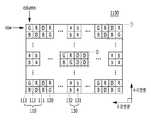
도 2a는 본 발명의 실시예에 따른 이미지 센서의 픽셀 어레이를 도시한 평면도이고, 도 2b 및 도 2c는 변형예들을 도시한 평면도이다. 여기서, 도 2a 내지 도 2c는 도 1에 도시된 픽셀 어레이의 일례를 도시한 것이다.FIG. 2A is a plan view showing a pixel array of an image sensor according to an embodiment of the present invention, and FIGS. 2B and 2C are plan views showing modifications. Here, Figs. 2A to 2C show an example of the pixel array shown in Fig.
도 2a에 도시된 바와 같이, 실시예에 따른 이미지 센서의 픽셀 어레이(1100)는 복수의 픽셀들이 2차원적으로 배열되고, 복수의 픽셀들은 복수의 컬러 검출 픽셀(110), 복수의 깊이 검출 픽셀(120) 및 복수의 위상차 검출 픽셀(130)을 포함할 수 있다. 여기서, 컬러 검출 픽셀(110)은 베이어 배열(Bayer arrangement)에 따라 규칙적으로 배열될 수 있고, 깊이 검출 픽셀(120) 및 위상차 검출 픽셀(130)은 특정 위치의 컬러 검출 픽셀(110)을 대체하는 방식으로 랜덤하게 배치될 수 있다. 그리고, 위상차 검출 픽셀(130)은 각각 서로 다른 방향으로 편심된 오픈부를 갖는 차광층을 포함하는 두 픽셀(131, 132)을 단위그룹으로 하여 랜덤하게 배치될 수 있다.2A, a
픽셀 어레이(1100)에서 각각의 행(row) 또는/및 열(column)마다 복수의 컬러 검출 픽셀(110) 및 하나 이상의 깊이 검출 픽셀(120)이 배치될 수 있다. 여기서, 둘 이상의 위상차 검출 픽셀(130)은 각각의 행 또는/및 열마다 배치되거나, 또는 어느 하나 이상의 행 또는/및 열에 배치될 수 있다.A plurality of
또한, 픽셀 어레이(1100)에서 각각의 행 또는/및 열마다 복수의 컬러 검출 픽셀(110)이 배치되고, 어느 하나 이상의 행 또는/및 열에서 하나 이상의 깊이 검출 픽셀(120)이 배치될 수 있다. 여기서, 둘 이상의 위상차 검출 픽셀(130)은 깊이 검출 픽셀(120)이 배치되는 행 또는/및 열에 배치되거나, 또는 깊이 검출 픽셀(120)이 배치되지 않은 행 또는/및 열에 배치될 수 있다.In addition, a plurality of
컬러 검출 픽셀(110)은 제1컬러픽셀(111), 제2컬러픽셀(112) 및 제3컬러픽셀(113)을 포함할 수 있으며, 제1컬러픽셀(111) 내지 제3컬러픽셀(113)은 베이어 패턴 타입으로 배열될 수 있다. 제1컬러픽셀(111)은 레드픽셀(R)일 수 있고, 제2컬러픽셀(112)은 그린픽셀(G)일 수 있으며, 제3컬러픽셀(113)은 블루픽셀(B)일 수 있다. 한편, 제1컬러픽셀(111) 내지 제3컬러픽셀(113)은 각각 사이안픽셀(Cyan pixel), 마젠타픽셀(Magenta pixel) 및 옐로우픽셀(Yellow pixel)일 수도 있다.The
깊이 검출 픽셀(120)은 베이어 패턴 타입으로 배열된 복수의 컬러 검출 픽셀(110)들 중에서 랜덤하게 어느 하나의 컬러 검출 픽셀(110)을 대체하여 배치될 수 있다. 예를 들어, 깊이 검출 픽셀(120)은 2×2 어레이에서 두 개가 배치되는 제2컬러픽셀(112) 즉, 그린픽셀(G) 중 어느 하나를 대체하여 배치될 수 있다(도면부호 ① 참조). 또한, 깊이 검출 픽셀(120)은 2×4 어레이에서 2×2 어레이에는 컬러 검출 픽셀(110)이 배치되고, 나머지 2×2 어레이에 대응하는 컬러 검출 픽셀(110) 모두를 깊이 검출 픽셀(120)로 대체하여 배치될 수도 있다(도면부호 ② 참조).The
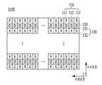
이어서, 도 2b를 참조하면 픽셀 어레이(1100)에서 컬러 검출 픽셀(110), 깊이 검출 픽셀(120) 및 위상차 검출 픽셀(130)은 행 단위로 배치될 수 있다. 즉, 픽셀 어레이(1100)는 컬러 검출 픽셀(110)만이 배치된 행(이하, 제1행), 깊이 검출 픽셀(120)만이 배치된 행(이하, 제2행) 및 위상차 검출 픽셀(130)만이 배치된 행(이하, 제3행)을 포함할 수 있다. 여기서, 제1행 내지 제3행은 수직방향으로 복수회 순차적으로 배치되거나, 또는 랜덤하게 배치될 수 있다. 한편, 픽셀 어레이(1100)에서 컬러 검출 픽셀(110), 깊이 검출 픽셀(120) 및 위상차 검출 픽셀(130) 열 단위로 배치될 수도 있다.2B, the
이어서, 도 2c를 참조하면 픽셀 어레이(1100)에서 컬러 검출 픽셀(110), 깊이 검출 픽셀(120) 및 위상차 검출 픽셀(130)은 블럭(또는 영역) 단위로 배치될 수 있다. 각각의 픽셀이 배치되는 블럭은 하나이거나, 또는 그 이상일 수 있다. 각각의 픽셀이 배치되는 블럭의 면적 및 형상은 요구되는 특성에 따라 조절할 수 있다.
Referring to FIG. 2C, the
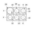
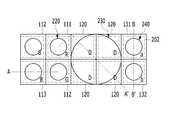
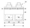
도 3a는 본 발명의 제1실시예에 따른 이미지 센서의 픽셀 어레이 일부를 도시한 평면도이고, 도 3b는 본 발명의 제1실시예에 따른 컬러 검출 픽셀 및 깊이 검출 픽셀을 도 3a에 도시된 A-A'절취선을 따라 도시한 단면도이다. 도 4a는 본 발명의 제2실시예에 따른 이미지 센서의 픽셀 어레이 일부를 도시한 평면도이고, 도 4b는 본 발명의 제2실시예에 따른 컬러 검출 픽셀 및 깊이 검출 픽셀을 도 4a에 도시된 A-A'절취선을 따라 도시한 단면도이다. 그리고, 도 5는 본 발명의 제1 및 제2실시예에 따른 이미지 센서의 위상차 검출 픽셀에 적용 가능한 일례를 도 3a 및 도 4a에 도시된 B-B'절취선을 따라 도시한 단면도이다.3A is a plan view showing a part of the pixel array of the image sensor according to the first embodiment of the present invention, and FIG. 3B is a cross-sectional view of the color detecting pixel and the depth detecting pixel according to the first embodiment of the present invention, Sectional view along the -A 'perforation line. 4A is a plan view showing a part of the pixel array of the image sensor according to the second embodiment of the present invention, and FIG. 4B is a plan view showing the color detecting pixel and the depth detecting pixel according to the second embodiment of the present invention, Sectional view along the -A 'perforation line. 5 is a cross-sectional view of the phase difference detecting pixel of the image sensor according to the first and second embodiments of the present invention, taken along line B-B 'in FIG. 3A and FIG. 4A.
먼저, 도 3a, 도 3b, 도 4a 및 도 4b에 도시된 바와 같이, 실시예들에 따른 이미지 센서는 복수의 컬러 검출 픽셀(110) 및 복수의 깊이 검출 픽셀(120)을 포함한 복수의 픽셀들이 2차원 배열된 픽셀 어레이 및 각각의 픽셀들에 대응하는 광전변환층(202)을 포함할 수 있다. 여기서, 각각의 컬러 검출 픽셀(110) 및 각각의 깊이 검출 픽셀(120)에 대응하는 광전변환층(202)은 동일한 수광면적 및 깊이를 가질 수 있다. 또한, 각각의 컬러 검출 픽셀(110) 및 각각의 깊이 검출 픽셀(120)에 대응하는 광전변환층(202)은 동일한 수광면적을 갖고, 각각의 컬러 검출 픽셀(110)에 대응하는 광전변환층(202)의 깊이보다 각각의 깊이 검출 픽셀(120)에 대응하는 광전변환층(202)의 깊이가 더 클 수도 있다. 이 경우, 깊이 검출 픽셀(120)의 양자효율 및 피사체까지의 초점거리를 보다 효과적으로 증대시킬 수 있다.3A, 3B, 4A, and 4B, the image sensor according to embodiments includes a plurality of pixels including a plurality of
광전변환층(202)은 기판(201)에 형성된 것일 수 있다. 기판(201)에 형성된 광전변환층(202)은 수직적으로 중첩되는 복수의 광전변환부들을 포함할 수 있다. 광전변환부 각각은 N형 불순물영역과 P형 불순물영역을 포함하는 포토다이오드(Photo Diode)일 수 있다. 기판(201)은 반도체 기판일 수 있으며, 단결정 상태(Single crystal state)의 실리콘 함유 재료를 포함할 수 있다.The
실시예들에 따른 이미지 센서에서 복수의 컬러 검출 픽셀(110)은 제1컬러픽셀(111), 제2컬러픽셀(112) 및 제3컬러픽셀(113)을 포함할 수 있다. 제1컬러픽셀(111)은 레드픽셀(R)일 수 있고, 제2컬러픽셀(112)은 그린픽셀(G)일 수 있으며, 제3컬러픽셀(113)은 블루픽셀(B)일 수 있다.In the image sensor according to the embodiments, the plurality of
각각의 컬러 검출 픽셀(110) 즉, 제1컬러픽셀(111) 내지 제3컬러픽셀(113)은 광전변환층(202), 광전변환층(202) 상의 대역필터층(210), 대역필터층(210) 상의 절연층(205) 및 절연층(205) 상의 제1집광층(220)을 포함할 수 있다. 여기서, 절연층(205)은 광전변환층(202)을 포함한 기판(201) 전면에서 대역필터층(210)을 덮도록 형성된 것으로, 제1집광층(220)의 특성을 향상시키기 위해 평탄한 표면을 가질 수 있다.Each
복수의 컬러 검출 픽셀(110)에서 대역필터층(210)은 입사광에서 특정 파장 대역만을 통과시키는 것으로, 실질적으로 컬러필터의 기능을 수행할 수 있다. 이를 위해, 대역필터층(210)은 제1컬러픽셀(111), 제2컬러픽셀(112) 및 제3컬러픽셀(113)에 대응하는 두께가 각각 상이할 수 있다. 구체적으로, 제1컬러픽셀(111)에 형성된 제1대역필터층(211)의 두께는 제2컬러픽셀(112)에 형성된 제2대역필터층(212)의 두께보다 클 수 있고, 제2대역필터층(212)의 두께는 제3컬러픽셀(113)에 형성된 제3대역필터층(213)의 두께보다 클 수 있다. 대역필터층(210)은 광전변환층과 제1집광층 사이에 위치하기 때문에 인접한 픽셀 사이의 광학적 크로스토크를 효과적으로 방지할 수 있다. 대역필터층(210)은 서로 다른 굴절률을 갖는 복수의 필터층이 교번 적층된 적층구조물일 수 있다. 필터층은 산화물, 질화물 또는 산화질화물을 포함할 수 있다. 일례로, 대역필터층(210)은 제1필터층(203)과 제2필터층(204)이 교번 적층된 적층구조물로 제1필터층(203)은 알루미늄질화물 또는 실리콘산화물을 포함할 수 있고, 제2필터층(204)은 실리콘질화물 또는 티타늄산화물을 포함할 수 있다.In the plurality of
제1집광층(220)은 상부층이 하부층보다 작은 직경을 갖는 복수의 물질층이 적층된 적층구조물이거나, 또는 반구형 렌즈일 수 있다. 여기서, 복수의 물질층은 산화물, 질화물 또는 산화질화물을 포함할 수 있다. 도면에 도시된 바와 같이, 제1집광층(220)이 적층구조물인 경우에는 제1층(221) 및 제1층(221) 상에 형성되어 제1층(221)보다 작은 직경을 갖는 제2층(222)을 포함할 수 있다. 여기서, 제1층(221)과 제2층(222)은 서로 동일한 물질이거나, 또는 서로 상이한 물질일 수 있다. 일례로, 제1층(221)은 실리콘질화물을 포함할 수 있고, 제2층(222)은 실리콘산화물을 포함할 수 있다. 그리고, 제1층(221)의 두께(t1)와 제2층(222)의 두께(t2)는 서로 동일하거나(t1 = t2), 또는 서로 상이할 수 있다(t1 ≠ t2). 이때, 제1집광층(220)의 두께(T1, T1 = t1 + t2)가 고정된 상태에서 제1층(221)의 두께(t1)와 제2층(222)의 두께(t2)를 조절하는 방법으로 피사체까지의 초점거리를 조절할 수 있다. 예를 들어, 제1집광층(220)의 두께(T1)가 고정된 상태에서 제1층(221)의 두께(t1)와 제2층(222)의 두께(t2)는 반비례관계를 가질 수 있다. 따라서, 제1층(221)의 두께(t1)가 증가할수록 초점거리가 짧아질 수 있고, 제1층(221)의 두께(t1)가 감소할수록 초점거리가 길어질 수 있다.The first light-
실시예들에 따른 이미지 센서에서 각각의 깊이 검출 픽셀(120)은 광전변환층(202), 광전변환층(202) 상의 절연층(205) 및 절연층(205) 상의 제2집광층(230)을 포함할 수 있다. 여기서, 각각의 깊이 검출 픽셀(120)에 일대일 대응하는 제2집광층(230)을 구비하거나(도 3a 및 도 3b 참조), 또는 둘 이상의 깊이 검출 픽셀(120)이 하나의 제2집광층(230)을 공유할 수 있다(도 4a 및 도 4b 참조).Each of the
각각의 깊이 검출 픽셀(120)에 대응하는 광전변환층(202)은 적외선을 수광할 수 있다. 따라서, 각각의 깊이 검출 픽셀(120)에 대응하는 광전변환층(202)의 깊이가 복수의 컬러 검출 픽셀(110)에 대응하는 광전변환층(202)의 깊이보다 클 경우 깊이 검출 픽셀(120)의 양자효율 및 초점거리를 보다 효과적으로 증대시킬 수 있다. 이는, 단결정 상태의 실리콘 함유 재료를 포함하는 기판(201)에 형성된 광전변환층(202)에서 적외선이 흡수되는 깊이가 가시광선이 흡수되는 깊이보다 깊기 때문이다.The
또한, 각각의 깊이 검출 픽셀(120)은 컬러 검출 픽셀(110)로부터 연장되어 광전변환층(202)과 제2집광층(230) 사이에 게재된 대역필터층(210)을 더 포함할 수도 있다(도 3a 및 도 3b 참조). 구체적으로, 깊이 검출 픽셀(120)에서의 대역필터층(210) 즉, 제4대역필터층(214)은 순수한 적외선만이 입사할 수 있도록 가시광선을 차단하는 역할을 수행한다. 이로써, 깊이 검출 픽셀로 입사되는 적외선의 세기(intensity)를 증가시켜 특성을 향상시킬 수 있다. 이를 위해, 컬러 검출 픽셀(110)에서의 대역필터층(210) 즉, 제1대역필터층(211) 내지 제3대역필터층(213)보다 깊이 검출 픽셀(120)에서의 제4대역필터층(214) 두께가 더 클 수 있다.Each of the
제2집광층(230)은 상부층이 하부층보다 작은 직경을 갖는 복수의 물질층이 적층된 적층구조물일 수 있다. 구체적으로, 제2집광층(230)은 제3층(231) 및 제3층(231) 상에 형성되어 제3층(231)보다 작은 직경을 갖는 제4층(232)을 포함할 수 있다. 제3층(231)과 제4층(232)은 서로 동일한 물질이거나, 또는 서로 상이한 물질일 수 있다. 일례로, 제3층(231)은 실리콘질화물을 포함할 수 있고, 제4층(232)은 실리콘산화물을 포함할 수 있다. 여기서, 제1집광층(220)이 복수의 물질층이 적층된 적층구조물인 경우에 제2집광층(230)의 제3층(231) 및 제4층(232)은 각각 제1집광층(220)의 제1층(221) 및 제2층(222)과 동일한 물질일 수 있다.The second light-
제2집광층(230)에서 제3층(231)의 두께(t3)와 제4층(232)의 두께(t4)는 서로 동일하거나(t3 = t4), 또는 서로 상이할 수 있다(t3 ≠ t4). 이때, 제2집광층(230)의 두께(T2, T2 = t3 + t4)가 고정된 상태에서 제3층(231)의 두께(t3)와 제4층(232)의 두께(t4)를 조절하는 방법으로 피사체까지의 초점거리를 조절할 수 있다. 예를 들어, 제2집광층(230)의 두께(T2)가 고정된 상태에서 제3층(231)의 두께(t3)와 제4층(232)의 두께(t4)는 반비례관계를 가질 수 있다. 따라서, 제3층(231)의 두께(t3)가 증가할수록 초점거리가 짧아질 수 있고, 제3층(231)의 두께(t3)가 감소할수록 초점거리가 길어질 수 있다.The thickness t3 of the
컬러 검출 픽셀(110)과 상이한 초점거리를 갖는 깊이 검출 픽셀(120)을 제공하기 위해 제2집광층(230)은 제1집광층(220)과 상이한 형상을 가질 수 있다. 구체적으로, 컬러 검출 픽셀(110)과 피사체 사이의 초점거리보다 깊이 검출 픽셀(120)과 피사체 사이의 초점거리가 더 길수록 정확한 깊이 정보를 생성할 수 있다. 이를 위해, 제2집광층(230)은 제1집광층(220)보다 큰 직경 또는 면적을 가질 수 있다. 면적 측면에서 컬러 검출 픽셀(110)의 광전변환층(202)과 깊이 검출 픽셀(120)의 광전변환층(202)이 서로 동일한 수광면적을 갖는 경우에 광전변환층(202)에 대응하는 제1집광층(220)의 면적보다 광전변환층(202)에 대응하는 제2집광층(230)의 면적이 더 클 수 있다. 이와 더불어서, 제2집광층(230)은 제1집광층(220)과 동일한 두께를 갖거나(T1 = T2), 또는 더 큰 두께를 가질 수 있다(T1〈 T2).The second light-
제1집광층(220) 및 제2집광층(230)이 모두 복수의 물질층이 적층된 적층구조물인 경우에 컬러 검출 픽셀(110)의 초점거리보다 긴 초점거리를 갖는 깊이 검출 픽셀(120)을 제공하기 위해 제1집광층(220)의 최하층 직경 또는 면적이 제2집광층(230)의 최하층 직경 또는 면적보다 작을 수 있다. 구체적으로, 제1집광층(220)의 제1층(221) 직경 또는 면적이 제2집광층(230)의 제3층(231) 직경 또는 면적보다 작을 수 있다. 아울러, 제1집광층(220)의 두께(T1)와 제2집광층(230)의 두께(T2)가 동일한 경우에 제1집광층(220)의 최하층 두께보다 제2집광층(230)의 최하층 두께가 더 얇을 수 있다. 구체적으로, 제1집광층(220)의 두께(T1)와 제2집광층(230)의 두께(T2)가 서로 동일한 경우에 제1집광층(220)의 제1층(221) 두께(t1)보다 제2집광층(230)의 제3층(231) 두께(t2)가 더 작을 수 있다.The
또한, 도 3a, 도 4a 및 도 5에 도시된 바와 같이, 실시예들에 따른 이미지 센서의 픽셀 어레이에서 복수의 픽셀들은 복수의 위상차 검출 픽셀(130)을 더 포함할 수 있다. 복수의 위상차 검출 픽셀(130)은 광전변환층(202)의 광축(또는 중심축)을 기준으로 서로 다른 방향으로 편심된(eccentrically) 오픈부(251A, 252A)를 갖는 차광층(251, 252)을 포함한 제1픽셀(131) 및 제2픽셀(132)을 포함할 수 있다.In addition, as shown in FIGS. 3A, 4A, and 5, in the pixel array of the image sensor according to the embodiments, the plurality of pixels may further include a plurality of phase
각각의 위상차 검출 픽셀(130)은 광전변환층(202), 광전변환층(202) 상이 절연층(205), 절연층(205) 내에 형성되고 광전변환층(202)의 광축에 대해 편심된 오픈부(251A, 252A)를 갖는 차광층(251, 252) 및 절연층(205) 상의 제3집광층(240)을 포함할 수 있다. 제3집광층(240)은 상부층이 하부층보다 작은 직경을 갖는 복수의 물질층이 적층된 적층구조물 또는 반구형 렌즈를 포함할 수 있다. 제3집광층(240)은 제2집광층(230)과 동일한 것일 수 있다.Each of the phase
상술한 바와 같이, 실시예에 따른 이미지 센서는 서로 다른 초점거리를 갖는 컬러 검출 픽셀(110) 및 깊이 검출 픽셀(120)을 구비함으로써, 외부환경(예컨대, 고조도 환경)에 대한 간섭을 억제할 수 있고, 정확한 깊이 정보를 생성할 수 있다. 또한, 구조가 단순하고, 양산이 용이하여 생산비용을 감소시킬 수 있다.As described above, the image sensor according to the embodiment has the
아울러, 위상차 검출 픽셀(130)을 더 포함함으로써, 더 정확한 깊이 정보를 생성할 수 있다.
In addition, by further including the phase
이하에서는, 도 1 내지 도 5에 도시된 실시예들에 따른 이미지 센서를 이용하여 깊이 정보를 생성하는 방법에 대하여 도 6 및 도 7을 참조하여 상세히 설명하기로 한다.Hereinafter, a method of generating depth information using the image sensor according to the embodiments shown in FIGS. 1 to 5 will be described in detail with reference to FIGS. 6 and 7. FIG.
도 6은 본 발명의 실시예에 따른 이미지 센서에서 ISP를 간략히 도시한 블럭도이다. 그리고, 도 7은 본 발명의 실시예에 따른 이미지 센서에서 깊이 정보를 생성하는 방법을 설명하기 위한 플로우 차트이다.6 is a block diagram schematically illustrating an ISP in an image sensor according to an embodiment of the present invention. 7 is a flowchart illustrating a method of generating depth information in an image sensor according to an embodiment of the present invention.
먼저, 도 1 및 도 6에 도시된 바와 같이, ISP(1110)는 픽셀 어레이로부터 CDS(1130), ADC(1140)를 통해 출력된 디지털 픽셀 신호(DPS)를 수신하여 이를 가공하는 기능을 수행한다. ISP(1110)는 제어부(310), 메모리부(320), 블러 가중치값 생성부(331)를 포함한 위상차 검출부(330), 에지 검출부(340) 및 깊이 검출부(350)를 포함할 수 있다.1 and 6, the
제어부(310)는 ISP(1110)내 모든 동작을 제어하는 기능을 수행할 수 있다. 메모리부(320)는 ISP(1110)로 전송된 디지털 픽셀 신호(DPS) 및 ISP(1110)에서 가공된 정보를 저장하는 기능을 수행할 수 있다. 위상차 검출부(330)는 픽셀 어레이 내 위상차 검출 픽셀의 출력 신호 또는 별도의 위상차 검출 센서에서 제공되는 신호를 이용하여 초점거리 측정, DOF(Depth Of Focus) 정보 생성등의 동작을 수행할 수 있다. 위상차 검출부(330) 내 블러 가중치값 생성부(331)는 보다 정확한 깊이 정보 생성이 가능하도록 초점거리에 기반한 블러 가중치값을 생성하는 기능을 수행할 수 있다. 에지 검출부(340)는 컬러 검출 픽셀 및 깊이 검출 픽셀의 디지털 픽셀 신호에서 에지값을 추출하는 기능을 수행할 수 있다. 그리고, 깊이 검출부(350)는 블러 가중치값 생성부(331)를 포함한 위상차 검출부(330) 및 에지 검출부(340)에서 제공되는 정보를 이용하여 깊이 정보를 생성하는 기능을 수행할 수 있다.The
이하, 도 6 및 도 7을 참조하여 실시예에 따른 이미지 센서를 이용한 깊이 정보 생성방법을 상세히 설명하기로 한다.Hereinafter, a depth information generating method using an image sensor according to an embodiment will be described in detail with reference to FIG. 6 and FIG.
먼저, 메모리부(320)에 소정 그룹의 디지털 픽셀 신호(DPS)를 로딩한다(S101). 여기서, 소정 그룹의 디지털 픽셀 신호(DPS)는 깊이 정보를 생성하는데 필요한 최소한의 정보 그룹을 의미한다. 예컨대, 디지털 픽셀 신호(DPS)가 행 단위로 제공되는 바, 소정 그룹의 디지털 픽셀 신호(DPS)는 한 행 단위 또는 수 내지 수십 행 단위의 정보일 수 있다. 그리고, 소정 그룹의 디지털 픽셀 신호(DPS)는 컬러 검출 픽셀의 출력 신호, 깊이 검출 픽셀의 출력 신호 및 위상차 검출 픽셀의 출력 신호를 모두 포함할 수 있다.First, a predetermined group of digital pixel signals DPS are loaded into the memory unit 320 (S101). Here, the digital pixel signal DPS of a predetermined group means a minimum information group necessary for generating depth information. For example, since the digital pixel signal DPS is provided on a row-by-row basis, the predetermined group of digital pixel signals DPS may be information on a one-row or several to several ten-row basis. The predetermined group of digital pixel signals DPS may include both the output signal of the color detection pixel, the output signal of the depth detection pixel, and the output signal of the phase difference detection pixel.
다음으로, 메모리부(320)에 로딩된 한 그룹의 디지털 픽셀 신호(DPS)로부터 피사체까지의 초점거리를 측정한다(S102). 여기서, 피사체까지의 초점거리는 위상차 검출 픽셀의 출력 신호를 이용하여 위상차 검출부(330)에서 산출할 수 있으며, 위상차에 따른 편차량으로부터 산출할 수 있다.Next, the focal length from the group of digital pixel signals DPS loaded in the
다음으로, 측정된 초첨거리와 사용자에 의해 설정된 초점거리가 일치하는지 여부를 판단한다(S103). 측정된 초첨거리와 사용자에 의해 설정된 초점거리가 일치할때까지 초점거리 측정(S102)를 반복 수행할 수 있다.Next, it is determined whether or not the measured focal distance matches the focal distance set by the user (S103). The focal distance measurement (S102) may be repeated until the measured focus distance matches the focal distance set by the user.
다음으로, 블러 가중치값을 산출한다(S104). 여기서, 블러 가중치값은 위상차 검출부(330)에서 DOF 정보를 생성한 후, 생성된 DOF 정보를 기준값으로하여 블러 가중치값 생성부(331)에서 피사체 앞에 초점이 잡힌 전핀(front-focusing or in-focus)과 피사체 뒤에 초점이 잡힌 후핀(back-focusing or out-focus)에 따른 위상차를 샘플링하여 블러 가중치값을 산출할 수 있다.Next, the blur weight value is calculated (S104). Here, the blur weight value is generated by the
다음으로, 컬러 검출 픽셀의 출력 신호를 이용하여 제1에지값을 추출한다(S105). 여기서, 컬러 검출 픽셀의 출력 신호는 제1컬러픽셀 내지 제3컬러픽셀의 신호를 의미할 수 있고, 제1에지값은 컬러 검출 픽셀에서 생성된 컬러 정보에서의 에지값을 의미할 수 있다. 예컨대, 제1에지값은 레드픽셀, 그린픽셀, 및 블루픽셀로부터 생성된 RGB정보에서의 에지값일 수 있다.Next, the first edge value is extracted using the output signal of the color detection pixel (S105). Here, the output signal of the color detection pixel may mean a signal of the first to third color pixels, and the first edge value may mean an edge value in the color information generated in the color detection pixel. For example, the first edge value may be a red pixel, a green pixel, and an edge value in RGB information generated from the blue pixel.
다음으로, 제1에지값 추출 여부를 판단한다(S106). 여기서, 제1에지값은 깊이 정보를 생성하기 위해 반드시 필요한 파라미터이다. 따라서, 제1에지값이 추출되지 않으면, 다음 차례의 디지털 픽셀 신호(DPS)를 메모리부(320)에 로딩한다(S201). 이후, 상술한 프로세스를 다시 순차적으로 진행한다.Next, it is determined whether or not the first edge value is extracted (S106). Here, the first edge value is a necessary parameter for generating the depth information. Accordingly, if the first edge value is not extracted, the next digital pixel signal DPS is loaded into the memory unit 320 (S201). Thereafter, the above-described process is sequentially performed again.
다음으로, 깊이 검출 픽셀의 출력 신호를 이용하여 제2에지값을 추출한다(S107). 이때, 제2에지값을 추출하기 위해서는 컬러 픽셀 출력 신호의 일부와 깊이 검출 픽셀의 신호를 이용할 수 있다. 구체적으로, 적외선으로부터 생성된 깊이 검출 픽셀 신호와 적외선과 인접한 파장 대역의 레드픽셀(예컨대, 제1컬러픽셀)로부터 생성된 컬러 검출 픽셀의 신호를 이용하여 제2에지값을 추출할 수 있다.Next, the second edge value is extracted using the output signal of the depth detection pixel (S107). In this case, in order to extract the second edge value, a part of the color pixel output signal and a signal of the depth detection pixel can be used. Specifically, the second edge value can be extracted using the depth detection pixel signal generated from infrared rays and the color detection pixel signal generated from the red pixel (for example, the first color pixel) in the wavelength band adjacent to the infrared ray.
다음으로, 제2에지값 추출 여부를 판단한다(S108). 여기서, 제2에지값은 제1에지값과 더불어서 깊이 정보를 생성하기 위해 반드시 필요한 파라미터이다. 따라서, 제2에지값이 추출되지 않으면, 다음 차례의 디지털 픽셀 신호(DPS)를 메모리부(320)에 로딩한다(S201). 이후, 상술한 프로세스를 다시 순차적으로 진행한다.Next, it is determined whether or not the second edge value is extracted (S108). Here, the second edge value is a necessary parameter in order to generate the depth information together with the first edge value. Accordingly, if the second edge value is not extracted, the next digital pixel signal DPS is loaded into the memory unit 320 (S201). Thereafter, the above-described process is sequentially performed again.
다음으로, 제1블러값 및 제2블러값을 생성한다(S109). 제1블러값 및 제2블러값은 포인트 스프레드 함수(point spread function, PSF)를 이용하여 추출된 제1에지값 및 제2에지값에 대한 블러의 크기값을 산출하고, 산출된 블러의 크기값에 기 산출된 블러 가중치값을 반영하여 생성할 수 있다. 여기서, 에지값과 포인트 스프레드 함수를 이용하여 산출된 블러의 크기값에 블러 가중치값을 반영하여 그 크기를 증폭할 수 있다.Next, a first blur value and a second blur value are generated (S109). The first blur value and the second blur value are obtained by calculating a magnitude value of a blur for a first edge value and a second edge value extracted using a point spread function (PSF) By reflecting the blur weight value calculated based on the blur weight value. Here, the magnitude of the blur weight value calculated using the edge value and the point spread function can be amplified by reflecting the blur weight value.
다음으로, 제1블러값과 제2블러값 사이의 차이를 통해 깊이 정보를 생성한다(S110).Next, the depth information is generated through the difference between the first blur value and the second blur value (S110).
상술한 바와 같이, 실시예에 따른 이미지 센서 및 이를 이용한 깊이 정보 생성 방법은 픽셀 어레이 내에 집적되고 서로 상이한 초점거리를 갖는 컬러 검출 픽셀 및 깊이 검출 픽셀을 이용하여 깊이 정보를 생성함으로써, 외부환경(예컨대, 고조도 환경)에 대한 간섭을 억제할 수 있고, 정확한 깊이 정보를 생성할 수 있다. 아울러, 위상차 검출 픽셀을 이용하여 더 정확한 깊이 정보를 생성할 수 있다.
As described above, the image sensor and the depth information generation method using the same according to the embodiment generate depth information using color detection pixels and depth detection pixels integrated in a pixel array and having different focal distances from each other, , High-contrast environment) can be suppressed, and accurate depth information can be generated. In addition, more accurate depth information can be generated using the phase difference detection pixels.
본 발명의 기술 사상은 상기 바람직한 실시예에 따라 구체적으로 기술되었으나, 상기 실시예는 그 설명을 위한 것이며, 그 제한을 위한 것이 아님을 주의하여야 한다. 또한, 본 발명의 기술분야의 통상의 전문가라면 본 발명의 기술사상의 범위내의 다양한 실시예가 가능함을 이해할 수 있을 것이다.
The technical idea of the present invention has been specifically described according to the above preferred embodiments, but it should be noted that the above embodiments are intended to be illustrative and not restrictive. In addition, it will be understood by those of ordinary skill in the art that various embodiments within the scope of the technical idea of the present invention are possible.
110 : 컬러 검출 픽셀120 : 깊이 검출 픽셀
201 : 기판202 : 광전변환층
205 : 절연층210 : 대역필터층
220 : 제1집광층230 : 제2집광층110: Color detection pixel 120: Depth detection pixel
201: substrate 202: photoelectric conversion layer
205 insulating
220: first condensing layer 230: second condensing layer
Claims (16)
Translated fromKorean각각의 상기 컬러 검출 픽셀은,
상기 광전변환층 상부의 제1집광층; 및
상기 광전변환층과 상기 제1집광층 사이에 게재된 대역필터층을 포함하며,
각각의 상기 깊이 검출 픽셀은,
상기 광전변환층 상부에서 상기 제1집광층 보다 큰 직경을 갖는 제2집광층을 포함하는 이미지 센서.
An image sensor having a photoelectric conversion layer formed so that a plurality of pixels including a plurality of color detecting pixels and a plurality of depth detecting pixels are two-dimensionally arranged and corresponding to each of the pixels,
Each of the color detection pixels comprising:
A first light-condensing layer on the photoelectric conversion layer; And
And a band-pass filter layer disposed between the photoelectric conversion layer and the first condensing layer,
Each of said depth detection pixels comprising:
And a second light-condensing layer having a larger diameter than the first light-condensing layer on the photoelectric conversion layer.
상기 광전변환층 상에 형성되어 층내 상기 대역필터층을 포함하여 평탄한 표면을 갖는 절연층을 더 포함하고, 상기 제1집광층 및 상기 제2집광층은 상기 절연층 상에 형성된 이미지 센서.
The method according to claim 1,
And an insulating layer formed on the photoelectric conversion layer and having a flat surface including the band-pass filter layer in the layer, wherein the first and second light-condensing layers are formed on the insulating layer.
상기 대역필터층은 상기 깊이 검출 픽셀로 연장되어 상기 광전변환층과 상기 제2집광층 사이에도 게재된 이미지 센서.
The method according to claim 1,
And the band filter layer extends between the photoelectric conversion layer and the second condensing layer.
상기 컬러 검출 픽셀에서의 대역필터층보다 상기 깊이 검출 픽셀에서의 대역필터층이 더 큰 두께를 갖는 이미지 센서.
The method of claim 3,
Wherein the band filter layer in the depth detection pixel has a greater thickness than the band filter layer in the color detection pixel.
하나의 상기 제2집광층을 둘 이상의 상기 깊이 검출 픽셀이 공유하는 이미지 센서.
The method according to claim 1,
Wherein at least two of the depth-detecting pixels share one of the second condensing layers.
상기 제1집광층의 두께는 상기 제2집광층의 두께와 동일하거나, 또는 더 작은 이미지 센서.
The method according to claim 1,
And the thickness of the first condensing layer is equal to or smaller than the thickness of the second condensing layer.
상기 제1집광층 및 상기 제2집광층은 상부층이 하부층보다 작은 직경을 갖는 복수의 물질층이 적층된 적층구조물을 포함하는 이미지 센서.
The method according to claim 1,
Wherein the first light-collecting layer and the second light-collecting layer include a laminated structure in which a plurality of material layers having a diameter smaller than that of the lower layer are stacked.
상기 제1집광층의 최하층 직경이 상기 제2집광층의 최하층 직경보다 작은 이미지 센서.
8. The method of claim 7,
And the lowest layer diameter of the first light-collecting layer is smaller than the lowest layer diameter of the second light-collecting layer.
상기 제1집광층과 상기 제2집광층의 두께가 동일한 경우에
상기 제1집광층의 최하층 두께보다 상기 제2집광층의 최하층 두께가 더 얇은 이미지 센서.
8. The method of claim 7,
When the thicknesses of the first and second light-condensing layers are the same
And the thickness of the lowermost layer of the second light-condensing layer is thinner than the thickness of the lowermost layer of the first light-condensing layer.
상기 제1집광층은 반구형 렌즈를 포함하고,
상기 제2집광층은 상부층이 하부층보다 작은 직경을 갖는 복수의 물질층이 적층된 적층구조물을 포함하는 이미지 센서.
The method according to claim 1,
Wherein the first light-condensing layer includes a hemispherical lens,
And the second light-condensing layer includes a laminated structure in which a plurality of material layers having a diameter smaller than that of the lower layer are stacked.
상기 대역필터층은 서로 다른 굴절률을 갖는 복수의 필터층이 교번 적층된 적층구조물을 포함하는 이미지 센서.
The method according to claim 1,
Wherein the band-pass filter layer comprises a laminated structure in which a plurality of filter layers having different refractive indices are alternately stacked.
상기 복수의 컬러 검출 픽셀은,
제1컬러픽셀, 제2컬러픽셀 및 제3컬러픽셀을 포함하고,
상기 제1컬러픽셀의 대역필터층은 상기 제2컬러픽셀의 대역필터층보다 큰 두께를 갖고,
상기 제2컬러픽셀의 대역필터층은 상기 제3컬러픽셀의 대역필터층보다 큰 두께를 갖는 이미지 센서,
The method according to claim 1,
Wherein the plurality of color detection pixels include:
A first color pixel, a second color pixel, and a third color pixel,
Wherein the band filter layer of the first color pixel has a thickness greater than the band filter layer of the second color pixel,
Wherein the band filter layer of the second color pixel comprises an image sensor having a thickness greater than the band filter layer of the third color pixel,
상기 제1컬러픽셀은 레드픽셀을 포함하고, 제2컬러픽셀은 그린픽셀을 포함하며, 상기 제3컬러픽셀은 블루픽셀을 포함하는 이미지 센서.
13. The method of claim 12,
Wherein the first color pixel comprises a red pixel, the second color pixel comprises a green pixel, and the third color pixel comprises a blue pixel.
상기 복수의 픽셀들은 복수의 위상차 검출 픽셀을 더 포함하고,
각각의 상기 위상차 검출 픽셀은,
상기 광전변환층 상부의 제3집광층; 및
상기 광전변환층과 상기 제3집광층 사이에 게재되어 상기 광전변환층의 광축에 대해 편심된 오픈부를 갖는 차광층
을 포함하는 이미지 센서.
The method according to claim 1,
Wherein the plurality of pixels further include a plurality of phase difference detection pixels,
Each of the phase difference detection pixels comprises:
A third light-converging layer above the photoelectric conversion layer; And
A light-shielding layer disposed between the photoelectric conversion layer and the third light-condensing layer and having an open portion eccentric to the optical axis of the photoelectric conversion layer,
.
상기 제3집광층은 상부층이 하부층보다 작은 직경을 갖는 복수의 물질층이 적층된 적층구조물 또는 반구형 렌즈를 포함하는 이미지 센서.
15. The method of claim 14,
And the third light-collecting layer includes a laminated structure or hemispherical lens in which a plurality of material layers having a diameter smaller than that of the lower layer are stacked.
상기 위상차 검출 픽셀로부터 블러 가중치값을 산출하는 단계;
상기 컬러 검출 픽셀로부터 제1에지값을 추출하는 단계;
상기 깊이 검출 픽셀로부터 제2에지값을 추출하는 단계;
상기 제1에지값 및 제2에지값과 포인트 스프레드 함수를 이용하여 제1블러값 및 제2블러값을 산출하는 단계;
산출된 상기 제1 및 제2블러값에 상기 블러 가중치값을 반영하여 제1 및 제2블러값을 증폭시키는 단계; 및
증폭된 상기 제1 및 제2블러값 차이를 이용하여 깊이 정보를 생성하는 단계
를 포함하는 깊이 정보 생성 방법.
An image sensor in which a plurality of pixels including a plurality of color detection pixels, a plurality of depth detection pixels, and a plurality of phase difference detection pixels are two-dimensionally arranged,
Calculating a blur weight value from the phase difference detection pixel;
Extracting a first edge value from the color detection pixel;
Extracting a second edge value from the depth detection pixel;
Calculating a first blur value and a second blur value using the first edge value and the second edge value and a point spread function;
Amplifying the first and second blur values by reflecting the blur weight values to the calculated first and second blur values; And
Generating depth information using the amplified first and second blur value differences
And generating a depth information.
Priority Applications (3)
| Application Number | Priority Date | Filing Date | Title |
|---|---|---|---|
| KR1020140112887AKR20160025729A (en) | 2014-08-28 | 2014-08-28 | Image sensor having depth detection pixel and method for depth date generation using the same |
| US14/532,838US9313432B2 (en) | 2014-08-28 | 2014-11-04 | Image sensor having depth detection pixels and method for generating depth data with the image sensor |
| CN201510044326.9ACN105991978B (en) | 2014-08-28 | 2015-01-28 | The method of imaging sensor and generation depth data with depth detection pixel |
Applications Claiming Priority (1)
| Application Number | Priority Date | Filing Date | Title |
|---|---|---|---|
| KR1020140112887AKR20160025729A (en) | 2014-08-28 | 2014-08-28 | Image sensor having depth detection pixel and method for depth date generation using the same |
Publications (1)
| Publication Number | Publication Date |
|---|---|
| KR20160025729Atrue KR20160025729A (en) | 2016-03-09 |
Family
ID=55404059
Family Applications (1)
| Application Number | Title | Priority Date | Filing Date |
|---|---|---|---|
| KR1020140112887AWithdrawnKR20160025729A (en) | 2014-08-28 | 2014-08-28 | Image sensor having depth detection pixel and method for depth date generation using the same |
Country Status (3)
| Country | Link |
|---|---|
| US (1) | US9313432B2 (en) |
| KR (1) | KR20160025729A (en) |
| CN (1) | CN105991978B (en) |
Families Citing this family (11)
| Publication number | Priority date | Publication date | Assignee | Title |
|---|---|---|---|---|
| KR102283423B1 (en)* | 2014-12-18 | 2021-07-30 | 엘지이노텍 주식회사 | Image pick-up apparatus, portable terminal including the same and image pick-up method using the apparatus |
| US10154234B2 (en)* | 2016-03-16 | 2018-12-11 | Omnivision Technologies, Inc. | Image sensor with peripheral 3A-control sensors and associated imaging system |
| KR102391632B1 (en)* | 2016-06-07 | 2022-04-27 | 애어리3디 인크. | Light field imaging device and depth acquisition and three-dimensional imaging method |
| CN107133982B (en)* | 2017-04-28 | 2020-05-15 | Oppo广东移动通信有限公司 | Depth map construction method and device, shooting equipment and terminal equipment |
| US12009379B2 (en)* | 2017-05-01 | 2024-06-11 | Visera Technologies Company Limited | Image sensor |
| US10410374B2 (en)* | 2017-12-28 | 2019-09-10 | Semiconductor Components Industries, Llc | Image sensors with calibrated phase detection pixels |
| US10985203B2 (en) | 2018-10-10 | 2021-04-20 | Sensors Unlimited, Inc. | Sensors for simultaneous passive imaging and range finding |
| KR102771998B1 (en)* | 2019-04-29 | 2025-02-25 | 엘지이노텍 주식회사 | Camera module |
| KR20210028808A (en) | 2019-09-04 | 2021-03-15 | 삼성전자주식회사 | Image sensor and imaging apparatus having the same |
| TWI718765B (en) | 2019-11-18 | 2021-02-11 | 大陸商廣州立景創新科技有限公司 | Image sensing device |
| CN112331684B (en)* | 2020-11-20 | 2024-02-09 | 联合微电子中心有限责任公司 | Image sensor and method of forming same |
Family Cites Families (10)
| Publication number | Priority date | Publication date | Assignee | Title |
|---|---|---|---|---|
| US9419035B2 (en)* | 2008-02-11 | 2016-08-16 | Omnivision Technologies, Inc. | Image sensor with color pixels having uniform light absorption depths |
| KR101467509B1 (en)* | 2008-07-25 | 2014-12-01 | 삼성전자주식회사 | Image sensor and operating method for image sensor |
| KR20100018449A (en)* | 2008-08-06 | 2010-02-17 | 삼성전자주식회사 | Pixel array of three dimensional image sensor |
| KR20100018851A (en) | 2008-08-07 | 2010-02-18 | 삼성전자주식회사 | Cmos image sensor including an ir cut filter and manufacturing method thereof |
| KR101648353B1 (en)* | 2009-09-25 | 2016-08-17 | 삼성전자 주식회사 | Image sensor having depth sensor |
| CN102483510B (en)* | 2009-11-20 | 2015-04-15 | 富士胶片株式会社 | Solid-state imaging device |
| KR20110061677A (en) | 2009-12-02 | 2011-06-10 | 삼성전자주식회사 | Image sensor and its manufacturing method. |
| JP2012222742A (en)* | 2011-04-13 | 2012-11-12 | Sony Corp | Imaging element and imaging apparatus |
| KR101696335B1 (en)* | 2012-01-10 | 2017-01-13 | 소프트키네틱 센서스 엔브이 | Multispectral sensor |
| KR102007279B1 (en)* | 2013-02-08 | 2019-08-05 | 삼성전자주식회사 | Depth pixel included in three-dimensional image sensor, three-dimensional image sensor including the same and method of operating depth pixel included in three-dimensional image sensor |
- 2014
- 2014-08-28KRKR1020140112887Apatent/KR20160025729A/ennot_activeWithdrawn
- 2014-11-04USUS14/532,838patent/US9313432B2/enactiveActive
- 2015
- 2015-01-28CNCN201510044326.9Apatent/CN105991978B/enactiveActive
Also Published As
| Publication number | Publication date |
|---|---|
| US20160065870A1 (en) | 2016-03-03 |
| CN105991978B (en) | 2018-07-17 |
| CN105991978A (en) | 2016-10-05 |
| US9313432B2 (en) | 2016-04-12 |
Similar Documents
| Publication | Publication Date | Title |
|---|---|---|
| KR20160025729A (en) | Image sensor having depth detection pixel and method for depth date generation using the same | |
| CN206947348U (en) | Imaging sensor | |
| KR102437162B1 (en) | Image sensor | |
| CN206727071U (en) | Imaging sensor | |
| US9749521B2 (en) | Image sensor with in-pixel depth sensing | |
| CN101545771B (en) | Range sensor and 3D color image sensor | |
| US20140198183A1 (en) | Sensing pixel and image sensor including same | |
| US10911738B2 (en) | Compound-eye imaging device | |
| US20130015545A1 (en) | Solid-state imaging device, manufacturing method of solid-state imaging device and electronic apparatus | |
| JP2015128131A (en) | Solid state image sensor and electronic apparatus | |
| KR102312964B1 (en) | Image sensor and method for fabricating the same | |
| US20130234029A1 (en) | Image sensor for two-dimensional and three-dimensional image capture | |
| JP2015230355A (en) | Imaging device and image pickup element | |
| KR20160016015A (en) | Image sensor for improving crosstalk characteristic and method thereof | |
| JP6716902B2 (en) | Electronics | |
| JP2015028960A (en) | Solid-state imaging device and electronic apparatus | |
| US9780132B2 (en) | Image sensor and electronic device including the same | |
| KR20120100232A (en) | Microlens, depth sensor having the microlens and method for fabricating the microlens | |
| US10115757B2 (en) | Image sensor and electronic device having the same | |
| US9583522B2 (en) | Image sensor and electronic device including the same | |
| KR20170037053A (en) | Image sensor | |
| JP2011151421A (en) | Solid-state image sensor, method of manufacturing the same, and imaging device | |
| KR102372736B1 (en) | Image sensor having phase difference detection pixel | |
| KR20160028196A (en) | Image sensor having the phase difference detection pixel | |
| JP5282797B2 (en) | Solid-state imaging device, manufacturing method of solid-state imaging device, and image photographing apparatus |
Legal Events
| Date | Code | Title | Description |
|---|---|---|---|
| PA0109 | Patent application | Patent event code:PA01091R01D Comment text:Patent Application Patent event date:20140828 | |
| PG1501 | Laying open of application | ||
| PC1203 | Withdrawal of no request for examination | ||
| WITN | Application deemed withdrawn, e.g. because no request for examination was filed or no examination fee was paid |