KR20160015447A - Lens, light source module, lighting device and lighting system - Google Patents
Lens, light source module, lighting device and lighting systemDownload PDFInfo
- Publication number
- KR20160015447A KR20160015447AKR1020140097209AKR20140097209AKR20160015447AKR 20160015447 AKR20160015447 AKR 20160015447AKR 1020140097209 AKR1020140097209 AKR 1020140097209AKR 20140097209 AKR20140097209 AKR 20140097209AKR 20160015447 AKR20160015447 AKR 20160015447A
- Authority
- KR
- South Korea
- Prior art keywords
- light
- light source
- lens
- incident
- source module
- Prior art date
- Legal status (The legal status is an assumption and is not a legal conclusion. Google has not performed a legal analysis and makes no representation as to the accuracy of the status listed.)
- Ceased
Links
Images


Classifications
- F—MECHANICAL ENGINEERING; LIGHTING; HEATING; WEAPONS; BLASTING
- F21—LIGHTING
- F21V—FUNCTIONAL FEATURES OR DETAILS OF LIGHTING DEVICES OR SYSTEMS THEREOF; STRUCTURAL COMBINATIONS OF LIGHTING DEVICES WITH OTHER ARTICLES, NOT OTHERWISE PROVIDED FOR
- F21V5/00—Refractors for light sources
- F21V5/04—Refractors for light sources of lens shape
- G—PHYSICS
- G02—OPTICS
- G02B—OPTICAL ELEMENTS, SYSTEMS OR APPARATUS
- G02B19/00—Condensers, e.g. light collectors or similar non-imaging optics
- G02B19/0004—Condensers, e.g. light collectors or similar non-imaging optics characterised by the optical means employed
- G02B19/0028—Condensers, e.g. light collectors or similar non-imaging optics characterised by the optical means employed refractive and reflective surfaces, e.g. non-imaging catadioptric systems
- G—PHYSICS
- G02—OPTICS
- G02B—OPTICAL ELEMENTS, SYSTEMS OR APPARATUS
- G02B19/00—Condensers, e.g. light collectors or similar non-imaging optics
- G02B19/0033—Condensers, e.g. light collectors or similar non-imaging optics characterised by the use
- G02B19/0047—Condensers, e.g. light collectors or similar non-imaging optics characterised by the use for use with a light source
- G02B19/0052—Condensers, e.g. light collectors or similar non-imaging optics characterised by the use for use with a light source the light source comprising a laser diode
- G02B19/0057—Condensers, e.g. light collectors or similar non-imaging optics characterised by the use for use with a light source the light source comprising a laser diode in the form of a laser diode array, e.g. laser diode bar
- G—PHYSICS
- G02—OPTICS
- G02B—OPTICAL ELEMENTS, SYSTEMS OR APPARATUS
- G02B19/00—Condensers, e.g. light collectors or similar non-imaging optics
- G02B19/0033—Condensers, e.g. light collectors or similar non-imaging optics characterised by the use
- G02B19/0047—Condensers, e.g. light collectors or similar non-imaging optics characterised by the use for use with a light source
- G02B19/0071—Condensers, e.g. light collectors or similar non-imaging optics characterised by the use for use with a light source adapted to illuminate a complete hemisphere or a plane extending 360 degrees around the source
- H—ELECTRICITY
- H05—ELECTRIC TECHNIQUES NOT OTHERWISE PROVIDED FOR
- H05B—ELECTRIC HEATING; ELECTRIC LIGHT SOURCES NOT OTHERWISE PROVIDED FOR; CIRCUIT ARRANGEMENTS FOR ELECTRIC LIGHT SOURCES, IN GENERAL
- H05B45/00—Circuit arrangements for operating light-emitting diodes [LED]
- H—ELECTRICITY
- H05—ELECTRIC TECHNIQUES NOT OTHERWISE PROVIDED FOR
- H05B—ELECTRIC HEATING; ELECTRIC LIGHT SOURCES NOT OTHERWISE PROVIDED FOR; CIRCUIT ARRANGEMENTS FOR ELECTRIC LIGHT SOURCES, IN GENERAL
- H05B45/00—Circuit arrangements for operating light-emitting diodes [LED]
- H05B45/20—Controlling the colour of the light
- H—ELECTRICITY
- H05—ELECTRIC TECHNIQUES NOT OTHERWISE PROVIDED FOR
- H05B—ELECTRIC HEATING; ELECTRIC LIGHT SOURCES NOT OTHERWISE PROVIDED FOR; CIRCUIT ARRANGEMENTS FOR ELECTRIC LIGHT SOURCES, IN GENERAL
- H05B45/00—Circuit arrangements for operating light-emitting diodes [LED]
- H05B45/30—Driver circuits
- H—ELECTRICITY
- H10—SEMICONDUCTOR DEVICES; ELECTRIC SOLID-STATE DEVICES NOT OTHERWISE PROVIDED FOR
- H10H—INORGANIC LIGHT-EMITTING SEMICONDUCTOR DEVICES HAVING POTENTIAL BARRIERS
- H10H20/00—Individual inorganic light-emitting semiconductor devices having potential barriers, e.g. light-emitting diodes [LED]
- H10H20/80—Constructional details
- H10H20/85—Packages
- H10H20/855—Optical field-shaping means, e.g. lenses
- F—MECHANICAL ENGINEERING; LIGHTING; HEATING; WEAPONS; BLASTING
- F21—LIGHTING
- F21K—NON-ELECTRIC LIGHT SOURCES USING LUMINESCENCE; LIGHT SOURCES USING ELECTROCHEMILUMINESCENCE; LIGHT SOURCES USING CHARGES OF COMBUSTIBLE MATERIAL; LIGHT SOURCES USING SEMICONDUCTOR DEVICES AS LIGHT-GENERATING ELEMENTS; LIGHT SOURCES NOT OTHERWISE PROVIDED FOR
- F21K9/00—Light sources using semiconductor devices as light-generating elements, e.g. using light-emitting diodes [LED] or lasers
- F21K9/20—Light sources comprising attachment means
- F21K9/23—Retrofit light sources for lighting devices with a single fitting for each light source, e.g. for substitution of incandescent lamps with bayonet or threaded fittings
- F—MECHANICAL ENGINEERING; LIGHTING; HEATING; WEAPONS; BLASTING
- F21—LIGHTING
- F21K—NON-ELECTRIC LIGHT SOURCES USING LUMINESCENCE; LIGHT SOURCES USING ELECTROCHEMILUMINESCENCE; LIGHT SOURCES USING CHARGES OF COMBUSTIBLE MATERIAL; LIGHT SOURCES USING SEMICONDUCTOR DEVICES AS LIGHT-GENERATING ELEMENTS; LIGHT SOURCES NOT OTHERWISE PROVIDED FOR
- F21K9/00—Light sources using semiconductor devices as light-generating elements, e.g. using light-emitting diodes [LED] or lasers
- F21K9/20—Light sources comprising attachment means
- F21K9/27—Retrofit light sources for lighting devices with two fittings for each light source, e.g. for substitution of fluorescent tubes
- F—MECHANICAL ENGINEERING; LIGHTING; HEATING; WEAPONS; BLASTING
- F21—LIGHTING
- F21K—NON-ELECTRIC LIGHT SOURCES USING LUMINESCENCE; LIGHT SOURCES USING ELECTROCHEMILUMINESCENCE; LIGHT SOURCES USING CHARGES OF COMBUSTIBLE MATERIAL; LIGHT SOURCES USING SEMICONDUCTOR DEVICES AS LIGHT-GENERATING ELEMENTS; LIGHT SOURCES NOT OTHERWISE PROVIDED FOR
- F21K9/00—Light sources using semiconductor devices as light-generating elements, e.g. using light-emitting diodes [LED] or lasers
- F21K9/60—Optical arrangements integrated in the light source, e.g. for improving the colour rendering index or the light extraction
- F—MECHANICAL ENGINEERING; LIGHTING; HEATING; WEAPONS; BLASTING
- F21—LIGHTING
- F21V—FUNCTIONAL FEATURES OR DETAILS OF LIGHTING DEVICES OR SYSTEMS THEREOF; STRUCTURAL COMBINATIONS OF LIGHTING DEVICES WITH OTHER ARTICLES, NOT OTHERWISE PROVIDED FOR
- F21V23/00—Arrangement of electric circuit elements in or on lighting devices
- F21V23/04—Arrangement of electric circuit elements in or on lighting devices the elements being switches
- F21V23/0442—Arrangement of electric circuit elements in or on lighting devices the elements being switches activated by means of a sensor, e.g. motion or photodetectors
- F21V23/045—Arrangement of electric circuit elements in or on lighting devices the elements being switches activated by means of a sensor, e.g. motion or photodetectors the sensor receiving a signal from a remote controller
- F—MECHANICAL ENGINEERING; LIGHTING; HEATING; WEAPONS; BLASTING
- F21—LIGHTING
- F21V—FUNCTIONAL FEATURES OR DETAILS OF LIGHTING DEVICES OR SYSTEMS THEREOF; STRUCTURAL COMBINATIONS OF LIGHTING DEVICES WITH OTHER ARTICLES, NOT OTHERWISE PROVIDED FOR
- F21V29/00—Protecting lighting devices from thermal damage; Cooling or heating arrangements specially adapted for lighting devices or systems
- F21V29/50—Cooling arrangements
- F21V29/502—Cooling arrangements characterised by the adaptation for cooling of specific components
- F21V29/507—Cooling arrangements characterised by the adaptation for cooling of specific components of means for protecting lighting devices from damage, e.g. housings
- F—MECHANICAL ENGINEERING; LIGHTING; HEATING; WEAPONS; BLASTING
- F21—LIGHTING
- F21V—FUNCTIONAL FEATURES OR DETAILS OF LIGHTING DEVICES OR SYSTEMS THEREOF; STRUCTURAL COMBINATIONS OF LIGHTING DEVICES WITH OTHER ARTICLES, NOT OTHERWISE PROVIDED FOR
- F21V29/00—Protecting lighting devices from thermal damage; Cooling or heating arrangements specially adapted for lighting devices or systems
- F21V29/50—Cooling arrangements
- F21V29/70—Cooling arrangements characterised by passive heat-dissipating elements, e.g. heat-sinks
- F21V29/74—Cooling arrangements characterised by passive heat-dissipating elements, e.g. heat-sinks with fins or blades
- F21V29/76—Cooling arrangements characterised by passive heat-dissipating elements, e.g. heat-sinks with fins or blades with essentially identical parallel planar fins or blades, e.g. with comb-like cross-section
- F21V29/763—Cooling arrangements characterised by passive heat-dissipating elements, e.g. heat-sinks with fins or blades with essentially identical parallel planar fins or blades, e.g. with comb-like cross-section the planes containing the fins or blades having the direction of the light emitting axis
- F—MECHANICAL ENGINEERING; LIGHTING; HEATING; WEAPONS; BLASTING
- F21—LIGHTING
- F21V—FUNCTIONAL FEATURES OR DETAILS OF LIGHTING DEVICES OR SYSTEMS THEREOF; STRUCTURAL COMBINATIONS OF LIGHTING DEVICES WITH OTHER ARTICLES, NOT OTHERWISE PROVIDED FOR
- F21V29/00—Protecting lighting devices from thermal damage; Cooling or heating arrangements specially adapted for lighting devices or systems
- F21V29/50—Cooling arrangements
- F21V29/70—Cooling arrangements characterised by passive heat-dissipating elements, e.g. heat-sinks
- F21V29/74—Cooling arrangements characterised by passive heat-dissipating elements, e.g. heat-sinks with fins or blades
- F21V29/77—Cooling arrangements characterised by passive heat-dissipating elements, e.g. heat-sinks with fins or blades with essentially identical diverging planar fins or blades, e.g. with fan-like or star-like cross-section
- F21V29/773—Cooling arrangements characterised by passive heat-dissipating elements, e.g. heat-sinks with fins or blades with essentially identical diverging planar fins or blades, e.g. with fan-like or star-like cross-section the planes containing the fins or blades having the direction of the light emitting axis
- F—MECHANICAL ENGINEERING; LIGHTING; HEATING; WEAPONS; BLASTING
- F21—LIGHTING
- F21Y—INDEXING SCHEME ASSOCIATED WITH SUBCLASSES F21K, F21L, F21S and F21V, RELATING TO THE FORM OR THE KIND OF THE LIGHT SOURCES OR OF THE COLOUR OF THE LIGHT EMITTED
- F21Y2105/00—Planar light sources
- F21Y2105/10—Planar light sources comprising a two-dimensional array of point-like light-generating elements
- F—MECHANICAL ENGINEERING; LIGHTING; HEATING; WEAPONS; BLASTING
- F21—LIGHTING
- F21Y—INDEXING SCHEME ASSOCIATED WITH SUBCLASSES F21K, F21L, F21S and F21V, RELATING TO THE FORM OR THE KIND OF THE LIGHT SOURCES OR OF THE COLOUR OF THE LIGHT EMITTED
- F21Y2115/00—Light-generating elements of semiconductor light sources
- F21Y2115/10—Light-emitting diodes [LED]
- H—ELECTRICITY
- H05—ELECTRIC TECHNIQUES NOT OTHERWISE PROVIDED FOR
- H05B—ELECTRIC HEATING; ELECTRIC LIGHT SOURCES NOT OTHERWISE PROVIDED FOR; CIRCUIT ARRANGEMENTS FOR ELECTRIC LIGHT SOURCES, IN GENERAL
- H05B45/00—Circuit arrangements for operating light-emitting diodes [LED]
- H05B45/20—Controlling the colour of the light
- H05B45/28—Controlling the colour of the light using temperature feedback
Landscapes
- Physics & Mathematics (AREA)
- General Physics & Mathematics (AREA)
- Optics & Photonics (AREA)
- Engineering & Computer Science (AREA)
- General Engineering & Computer Science (AREA)
- Non-Portable Lighting Devices Or Systems Thereof (AREA)
- Led Device Packages (AREA)
- Planar Illumination Modules (AREA)
- Microelectronics & Electronic Packaging (AREA)
Abstract
Translated fromKoreanDescription
Translated fromKorean본 발명은 발광소자 패키지용 렌즈, 광원 모듈, 조명 장치 및 조명 시스템에 관한 것이다.
The present invention relates to a lens, a light source module, a lighting device, and a lighting system for a light emitting device package.
발광소자 패키지에 사용되는 렌즈 중 광(廣)지향각 렌즈는 굴절을 이용하여 중심부에서 광을 측방향의 넓은 영역으로 확산시키는데 사용된다. 다만, 패키지의 다양한 광원 형태에 따라서 렌즈로 입사되는 광이 균일하게 확산되지 못하고 일부 영역에서 광 분포가 증가하는 경우가 발생한다. 이와 같이, 확산되는 광의 불균일한 분포에 의해 조명 장치 또는 디스플레이 장치에서 얼룩(mura)과 같은 광 균일도(Optical Uniformity)불량이 발생할 수 있다.
A wide diagonal lens among the lenses used in the light emitting device package is used to diffuse the light from the central portion to a wide side region by using the refraction. However, according to various light source types of the package, the light incident on the lens may not be uniformly diffused, and the light distribution may increase in some areas. As described above, a nonuniform distribution of the diffused light may cause a defective optical uniformity such as a mura in an illumination device or a display device.
이에 당 기술분야에서는 얼룩의 발생을 방지하고 광 분포를 균일하게 할 수 있는 방안이 요구되고 있다.Accordingly, there is a need in the art for a method for preventing the occurrence of stains and for uniforming the light distribution.
다만, 본 발명의 목적은 이에만 제한되는 것은 아니며, 명시적으로 언급하지 않더라도 아래에서 설명하는 과제의 해결수단이나 실시 형태로부터 파악될 수 있는 목적이나 효과도 이에 포함된다고 할 것이다.
It should be understood, however, that the scope of the present invention is not limited thereto and that the objects and effects which can be understood from the solution means and the embodiments of the problems described below are also included therein.
본 발명의 일 실시 형태에 따른 발광소자 패키지용 렌즈는, 바닥면; 상기 바닥면의 중앙에서 상기 바닥면과 연결되며, 광원 상에 배치되어 상기 광원으로부터의 광이 입사하는 입사면; 및 상기 바닥면의 가장자리에서 상기 바닥면과 연결되며, 상기 광이 외부로 방출되는 출사면을 포함하며, 상기 바닥면은 상기 입사면과 연결되는 영역을 포함하는 중앙 영역이 상기 광원을 향하여 부분적으로 돌출된 비평판형 구조를 가질 수 있다.A lens for a light emitting device package according to an embodiment of the present invention includes: a bottom surface; An incident surface connected to the bottom surface at the center of the bottom surface, the incident surface being disposed on the light source and receiving light from the light source; And a bottom surface that is connected to the bottom surface at an edge of the bottom surface and includes an exit surface through which the light is emitted to the outside, the bottom surface having a central region including a region connected to the incident surface, It may have a protruded nonplanar structure.
상기 입사면은 상기 광원의 광축이 지나는 상기 바닥면의 중앙에서 상기 출사면 방향으로 함몰된 홈부의 표면을 이루며, 상기 바닥면은 상기 출사면과 연결되어 상기 중앙으로 연장되는 제1면, 상기 제1면의 연장된 끝단에서 절곡되어 상기 광원을 향해 연장되는 제2면, 및 상기 제2면의 끝단에서 절곡되어 상기 홈부를 향해 연장되는 제3면을 포함할 수 있다.Wherein the incident surface forms a surface of a groove portion recessed in the direction of the emission surface from the center of the bottom surface through which the optical axis of the light source passes, the bottom surface is a first surface connected to the emission surface and extending to the center, A second surface that is bent at an extended end of the first surface and extends toward the light source, and a third surface that is bent at the end of the second surface and extends toward the groove.
상기 제1면과 제3면은 상기 제2면의 길이만큼 단차를 이룰 수 있다.The first surface and the third surface may be stepped by the length of the second surface.
상기 제2면은 상기 제1면과 제3면에 수직하거나 비스듬히 경사질 수 있다.The second surface may be perpendicular or oblique to the first and third surfaces.
상기 제2면과 제3면은 상기 홈부를 둘러싸는 링 형상의 구조를 가질 수 있다.And the second surface and the third surface may have a ring-shaped structure surrounding the groove portion.
상기 홈부는 상기 광원과 마주하도록 배치될 수 있다.The groove may be arranged to face the light source.
상기 바닥면의 외곽 영역에서 돌출되는 지지부를 더 포함할 수 있다.And a support portion protruding from an outer region of the bottom surface.
본 발명의 일 실시 형태에 따른 발광소자 패키지용 렌즈는, 바닥면; 상기 바닥면의 중앙에 함몰 형성된 홈부를 이루며, 광원 상에 배치되어 상기 광원으로부터의 광이 입사하는 입사면; 상기 바닥면의 가장자리에서 상기 바닥면과 연결되며, 상기 광이 외부로 방출되는 출사면; 및 상기 바닥면의 상기 홈부 둘레를 따라 구비되며, 상기 광원을 향하여 돌출되어 상기 바닥면과 단차를 이루는 돌출부;를 포함할 수 있다.A lens for a light emitting device package according to an embodiment of the present invention includes: a bottom surface; An incidence surface formed on the light source and through which light from the light source is incident, An emitting surface connected to the bottom surface at an edge of the bottom surface and emitting the light to the outside; And a protrusion which is provided along the circumference of the groove on the bottom surface and protrudes toward the light source to form a step with the bottom surface.
상기 돌출부는 관통홀이 형성된 링 형상을 가지며, 상기 관통홀의 내측면은 상기 입사면과 연속하는 구조로 연결될 수 있다.The projecting portion has a ring shape having a through hole, and the inner side surface of the through hole can be connected to the incident surface in a continuous structure.
상기 돌출부는 상기 렌즈와 동일한 재질로 이루어질 수 있다.The protrusion may be made of the same material as the lens.
상기 돌출부는 표면에 광 산란을 위한 요철이 형성될 수 있다.The protrusions may be provided with irregularities on the surface for light scattering.
상기 돌출부에 인접하여 상기 바닥면에 구비되는 지지부를 더 포함하며, 상기 지지부는 상기 돌출부보다 상기 광원으로 더 돌출될 수 있다.And a supporting portion provided on the bottom surface adjacent to the protruding portion, wherein the supporting portion may protrude further than the protruding portion with the light source.
본 발명의 일 실시 형태에 따른 광원 모듈은, 발광소자; 상기 발광소자가 실장되는 기판; 및 상기 기판 상에 실장되며, 상기 발광소자 상에 배치되는 렌즈를 포함할 수 있다.A light source module according to an embodiment of the present invention includes: a light emitting element; A substrate on which the light emitting device is mounted; And a lens mounted on the substrate and disposed on the light emitting device.
본 발명의 일 실시 형태에 따른 조명 장치는, 전기 연결구조를 갖는 하우징; 및 상기 하우징에 장착되는 적어도 하나의 광원 모듈을 포함할 수 있다.An illumination device according to an embodiment of the present invention includes: a housing having an electrical connection structure; And at least one light source module mounted on the housing.
상기 하우징에 장착되며, 상기 적어도 하나의 광원 모듈을 덮는 커버를 더 포함할 수 있다.And a cover mounted on the housing and covering the at least one light source module.
본 발명의 일 실시 형태에 따른 조명 시스템은, 주변의 온도 및 습도 중 적어도 하나의 공기 조건을 측정하는 센싱부; 상기 센싱부에 의해 측정된 적어도 하나의 공기 조건을 설정값과 비교하는 제어부; 전원을 공급하는 구동부; 및 적어도 하나의 조명 장치를 포함하며, 상기 구동부에서 공급하는 전원에 따라 구동하는 조명부를 포함하며, 상기 제어부는 상기 비교 결과를 통해 상기 조명부의 색온도를 결정할 수 있다.An illumination system according to an embodiment of the present invention includes: a sensing unit for measuring at least one of an ambient temperature and a humidity; A control unit for comparing at least one air condition measured by the sensing unit with a set value; A driving unit for supplying power; And at least one lighting device, and an illumination unit driven according to a power source supplied from the driving unit, and the controller can determine a color temperature of the illumination unit based on the comparison result.
상기 적어도 하나의 조명 장치는 전기 연결구조를 갖는 하우징과, 상기 하우징에 장착되는 적어도 하나의 광원 모듈을 포함하며, 상기 적어도 하나의 광원 모듈은, 발광소자; 상기 발광소자가 실장되는 기판; 및 상기 기판 상에 실장되며, 상기 발광소자 상에 배치되는 렌즈를 포함하며, 상기 렌즈는 바닥면과, 상기 바닥면의 중앙에서 상기 바닥면과 연결되며 광원 상에 배치되어 상기 광원으로부터의 광이 입사하는 입사면과, 상기 바닥면의 가장자리에서 상기 바닥면과 연결되며 상기 광이 외부로 방출되는 출사면을 포함하며, 상기 바닥면은 상기 입사면과 연결되는 영역을 포함하는 중앙 영역이 상기 광원을 향하여 부분적으로 돌출된 비평판형 구조를 가질 수 있다.Wherein the at least one illumination device comprises: a housing having an electrical connection structure; and at least one light source module mounted on the housing, the at least one light source module comprising: a light emitting element; A substrate on which the light emitting device is mounted; And a lens mounted on the substrate, the lens being disposed on the light emitting device, the lens having a bottom surface, a bottom surface connected to the bottom surface at a center of the bottom surface, and disposed on the light source, And a central region including a region connected to the incident surface, wherein the central region is connected to the bottom surface at an edge of the bottom surface, And may have a partially flattened non-flat plate-like structure.
상기 입사면은 상기 광원의 광축이 지나는 상기 바닥면의 중앙에서 상기 출사면 방향으로 함몰된 홈부의 표면을 이루며, 상기 바닥면은 상기 출사면과 연결되어 상기 중앙으로 연장되는 제1면, 상기 제1면의 연장된 끝단에서 절곡되어 상기 광원을 향 연장되는 제2면, 및 상기 제2면의 끝단에서 절곡되어 상기 홈부를 향해 연장되는 제3면을 포함할 수 있다.Wherein the incident surface forms a surface of a groove portion recessed in the direction of the emission surface from the center of the bottom surface through which the optical axis of the light source passes, the bottom surface is a first surface connected to the emission surface and extending to the center, A second surface that is bent at an extended end of the first surface and extends toward the light source, and a third surface that is bent at an end of the second surface and extends toward the groove.
상기 제1면과 제3면은 상기 제2면의 길이만큼 단차를 이룰 수 있다.The first surface and the third surface may be stepped by the length of the second surface.
상기 조명부는 제1 색온도를 갖는 제1 광을 방출하는 제1 조명 장치와 제2 색온도를 갖는 제2 광을 방출하는 제2 조명 장치를 포함하며, 상기 제어부는 상기 제1 광과 제2 광을 혼합하여 상기 결정된 상기 조명부의 색온도를 갖는 광을 구현할 수 있다.
Wherein the illumination unit includes a first illuminator that emits a first light having a first color temperature and a second illuminator that emits a second light having a second color temperature, And the light having the determined color temperature of the illumination unit may be mixed.
본 발명의 일 실시 형태에 따르면, 얼룩의 발생을 방지하고 광 분포를 균일하게 할 수 있는 발광소자 패키지용 렌즈, 광원 모듈, 조명 장치 및 조명 시스템이 제공될 수 있다.According to an embodiment of the present invention, there can be provided a lens, a light source module, a lighting device, and a lighting system for a light emitting device package that can prevent the occurrence of stains and make the light distribution uniform.
본 발명의 다양하면서도 유익한 장점과 효과는 상술한 내용에 한정되지 않으며, 본 발명의 구체적인 실시 형태를 설명하는 과정에서 보다 쉽게 이해될 수 있을 것이다.
The various and advantageous advantages and effects of the present invention are not limited to the above description, and can be more easily understood in the course of describing a specific embodiment of the present invention.
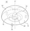
도 1은 본 발명의 일 실시 형태에 따른 발광소자 패키지용 렌즈를 개략적으로 나타내는 사시도이다.
도 2는 도 1의 단면도이다.
도 3은 도 1의 저면도이다.
도 4는 도 2의 렌즈에서 출사면의 변형예를 개략적으로 나타내는 단면도이다.
도 5는 본 발명의 다른 실시 형태에 따른 발광소자 패키지용 렌즈를 개략적으로 나타내는 단면도이다.
도 6은 도 5에서 돌출부를 개략적으로 나타내는 확대사시도이다.
도 7a 및 도 7b는 비교예에 따른 렌즈와 본 실시 형태에 따른 렌즈에서의 광 경로를 개략적으로 나타내는 단면도이다.
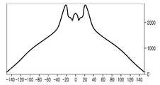
도 8a 및 도 8b는 각 렌즈에 의해 확산된 광 분포의 그래프이다.
도 9는 본 발명의 일 실시 형태에 따른 광원 모듈을 개략적으로 나타내는 단면도이다.
도 10a 및 도 10b는 도 9의 광원 모듈에 채용될 수 있는 발광소자의 다양한 예를 나타내는 단면도이다.
도 11은 CIE1931 좌표계이다.
도 12 내지 도 14는 본 발명의 일 실시 형태에 따른 발광소자에 채용될 수 있는 발광다이오드 칩의 다양한 예를 나타내는 단면도이다.
도 15는 본 발명의 일 실시 형태에 따른 조명 장치(벌브형)를 개략적으로 나타내는 분해사시도이다.
도 16은 본 발명의 일 실시 형태에 따른 조명 장치(L램프형)를 개략적으로 나타내는 분해사시도이다.
도 17은 본 발명의 일 실시 형태에 따른 조명 장치(평판형)를 개략적으로 나타내는 분해사시도이다.
도 18은 본 발명의 일 실시 형태에 따른 조명 시스템을 개략적으로 나타내는 블록도이다.
도 19는 도 18에 도시된 조명 시스템의 조명부의 상세 구성을 개략적으로 나타낸 블록도이다.
도 20은 도 18에 도시된 조명 시스템의 제어방법을 설명하기 위한 순서도이다.
도 21은 도 18에 도시된 조명 시스템을 개략적으로 구현한 사용 예시도이다.1 is a perspective view schematically showing a lens for a light emitting device package according to an embodiment of the present invention.
2 is a cross-sectional view of Fig.
3 is a bottom view of Fig.
Fig. 4 is a cross-sectional view schematically showing a modified example of the exit surface in the lens of Fig. 2;
5 is a cross-sectional view schematically showing a lens for a light emitting device package according to another embodiment of the present invention.
Fig. 6 is an enlarged perspective view schematically showing the projection in Fig. 5;
7A and 7B are cross-sectional views schematically showing a light path in the lens according to the comparative example and the lens according to the present embodiment.
8A and 8B are graphs of light distribution diffused by each lens.
9 is a cross-sectional view schematically showing a light source module according to an embodiment of the present invention.
10A and 10B are cross-sectional views showing various examples of light emitting devices that can be employed in the light source module of FIG.
11 is a CIE 1931 coordinate system.
12 to 14 are sectional views showing various examples of light emitting diode chips that can be employed in a light emitting device according to an embodiment of the present invention.
15 is an exploded perspective view schematically showing a lighting device (bulb type) according to an embodiment of the present invention.
16 is an exploded perspective view schematically showing a lighting apparatus (L lamp type) according to an embodiment of the present invention.
17 is an exploded perspective view schematically showing a lighting device (flat panel type) according to an embodiment of the present invention.
18 is a block diagram schematically showing an illumination system according to an embodiment of the present invention.
19 is a block diagram schematically showing a detailed configuration of an illumination unit of the illumination system shown in Fig.
20 is a flowchart for explaining the control method of the illumination system shown in Fig.
Fig. 21 is an example of a schematic implementation of the illumination system shown in Fig. 18;
이하, 첨부된 도면을 참조하여 본 발명의 바람직한 실시 형태들을 설명한다. 그러나, 본 발명의 실시형태는 여러 가지 다른 형태로 변형될 수 있으며, 본 발명의 범위가 이하 설명하는 실시 형태로 한정되는 것은 아니다.Hereinafter, preferred embodiments of the present invention will be described with reference to the accompanying drawings. However, the embodiments of the present invention can be modified into various other forms, and the scope of the present invention is not limited to the embodiments described below.
또한, 본 발명의 실시형태는 당해 기술분야에서 평균적인 지식을 가진 자에게 본 발명을 더욱 완전하게 설명하기 위해서 제공되는 것이다. 따라서, 도면에서 요소들의 형상 및 크기 등은 보다 명확한 설명을 위해 과장될 수 있으며, 도면 상의 동일한 부호로 표시되는 요소는 동일한 요소이다. 본 명세서에서, '상', '상부', '상면', '하', '하부', '하면', '측면' 등의 용어는 도면을 기준으로 한 것이며, 실제로는 소자나 구성요소가 배치되는 방향에 따라 달라질 수 있을 것이다.
Further, the embodiments of the present invention are provided to more fully explain the present invention to those skilled in the art. Accordingly, the shapes and sizes of the elements in the drawings may be exaggerated for clarity of description, and the elements denoted by the same reference numerals in the drawings are the same elements. In this specification, terms such as "upper,""upper,""upper,""lower,""lower,""lower,""side," and the like are based on the drawings, It will be possible to change depending on the direction.
도 1 내지 도 3을 참조하여 본 발명의 일 실시 형태에 따른 발광소자 패키지용 렌즈를 설명한다.1 to 3, a lens for a light emitting device package according to an embodiment of the present invention will be described.
도 1은 본 발명의 일 실시 형태에 따른 발광소자 패키지용 렌즈를 개략적으로 나타내는 사시도이고, 도 2는 도 1의 단면도이며, 도 3은 도 1의 저면도이다.
1 is a perspective view schematically showing a lens for a light emitting device package according to an embodiment of the present invention, Fig. 2 is a sectional view of Fig. 1, and Fig. 3 is a bottom view of Fig.
도 1 내지 도 3을 참조하면, 본 발명의 일 실시 형태에 따른 발광소자 패키지용 렌즈(10)는 광원(LS) 상에 배치되어 상기 광원(LS)에서 방출되는 광의 지향각을 조절할 수 있다. 여기서, 상기 광원(LS)은, 예를 들어, 발광소자 패키지를 포함할 수 있다. 그리고, 상기 렌즈(10)는 발광소자 패키지의 광을 확산시켜 넓은 지향각을 구현하는 광(廣)지향각 렌즈를 포함할 수 있다.
1 to 3, a
도 2 및 도 3에서 도시하는 바와 같이, 상기 렌즈(10)는 상기 광원(LS) 상에 배치되는 바닥면(11)과, 상기 광원(LS)의 광이 입사되는 입사면(12)과, 상기 광이 외부로 방출되는 출사면(13)을 포함할 수 있다.
2 and 3, the
상기 바닥면(11)은 상기 광원(LS)과 마주하는 면이며, 원 형상의 수평 단면 구조를 가질 수 있다. 상기 광원(LS)의 광축(Z)이 지나는 상기 바닥면(11)의 중앙에는 광출사 방향으로 함몰된 홈부(14)가 구비될 수 있다.
The
상기 홈부(14)는 상기 렌즈(10)의 중심을 지나는 광축(Z)에 대해 회전 대칭을 이루는 구조를 가지며, 그 표면은 상기 광원(LS)의 광이 입사되는 입사면(12)으로 정의될 수 있다. 즉, 상기 입사면(12)은 상기 홈부(14)의 표면을 이룰 수 있다. 따라서, 상기 광원(LS)에서 발생된 광은 상기 홈부(14) 내의 입사면(12)을 통과하여 상기 렌즈(10) 내부로 진행하게 된다.The
상기 홈부(14)는 상기 바닥면(11)을 통해 외부로 개방되며, 상기 광원(LS)의 상부에서 상기 광원(LS)과 마주하도록 배치될 수 있다.
The
한편, 상기 바닥면(11)은 상기 입사면(12)과 연결되는 중앙 영역이 상기 광원(LS)으로 부분적으로 돌출된 전체적으로 비평판형 구조를 가질 수 있다. 즉, 바닥면(11) 전체가 평평한 일반적인 구조와 달리 홈부(14) 둘레를 따라서 부분적으로 돌출된 구조를 가질 수 있다.
The
도 2 및 도 3에서 도시하는 바와 같이, 상기 바닥면(11)은 상기 출사면(13)과 연결되는 가장자리에서 상기 중앙 영역으로 연장되는 제1면(11a), 상기 제1면(11a)의 연장된 끝단에서 절곡되어 상기 광원(LS)을 향해 연장되는 제2면(11b), 및 상기 제2면(11b)의 끝단에서 절곡 및 연장되어 상기 입사면(12)과 연결되는 제3면(11c)을 포함할 수 있다.2 and 3, the
즉, 상기 바닥면(11)의 대부분에 해당하는 상기 제1면(11a)으로부터 상기 제2면(11b)과 제3면(11c)이 상기 홈부(14)를 둘러싸는 링 형상의 구조를 가지며 돌출될 수 있다. 상기 제3면(11c)은 상기 제1면(11a)과 평행을 이루며, 상기 제2면(11b)의 길이만큼 상기 제1면(11a)과 단차를 이룰 수 있다. 상기 제2면(11b)은 상기 제1면(11a)과 제3면(11c)에 수직하거나 비스듬히 경사지게 구비될 수 있다.
That is, the
상기 바닥면(11)은 외곽 영역에서 돌출되는 지지부(15)를 가질 수 있다. 외곽 영역은 상기 제2면(11b)과 제3면(11c)이 돌출된 중앙 영역에 대해 상대적으로 렌즈(10)의 가장자리에 인접한 영역으로 정의될 수 있다. 즉, 본 명세서에서 중앙 영역은 바닥면(11) 중 상기 제2면(11b)과 제3면(11c)이 돌출된 영역을 지칭하고, 외곽 영역은 상기 중앙 영역을 둘러싸는 상기 제1면(11a)이 차지하는 영역을 지칭하는 것으로 사용될 수 있다.
The
상기 지지부(15)는 상기 렌즈(10)와 일체를 이루거나 접착제 등을 통해 상기 외곽 영역에 해당하는 상기 제1면(11a)에 구비될 수 있다. 상기 지지부(15)는 복수개로 구비될 수 있으며, 상기 제3면(11c)보다 상기 광원(LS)으로 더 길게 돌출되어 연장될 수 있다.The
상기 지지부(15)는 상기 렌즈(10)가 예를 들어 기판 상에 장착되는 경우 상기 렌즈(10)를 고정 및 지지할 수 있다(도 9 참조). 즉, 상기 렌즈(10)는 상기 지지부(15)를 통해 상기 기판 상에 장착될 수 있다. 그리고, 상기 바닥면(11)은 상기 광원(LS) 상에 위치하고, 상기 입사면(12)은 상기 광원(LS)과 마주하도록 배치될 수 있다.
The
상기 출사면(13)은 상기 입사면(12)을 통해 상기 렌즈(10) 내부로 들어온 광이 외부로 방출되는 면으로 상기 렌즈(10)의 상면에 해당된다. 상기 출사면(13)은 상기 바닥면(11)과 연결되는 테두리로부터 상부 방향(광출사 방향)으로 돔 형태로 돌출되며, 상기 광축(Z)이 지나는 중앙이 상기 홈부(14)를 향해 오목하게 함몰되어 변곡점을 가지는 구조를 가질 수 있다. 구체적으로, 상기 출사면(13)은 상기 광축(Z)을 따라 상기 홈부(14)를 향해 함몰되어 오목한 곡면을 가지는 오목부(13a)와, 상기 오목부(13a)의 가장자리로부터 상기 테두리까지 연속하여 연장되는 볼록한 곡면을 가지는 볼록부(13b)를 포함할 수 있다.The
또한, 도 4에서 도시하는 바와 같이, 상기 출사면(13)은 전체적으로 상기 바닥면(11)과 연결되는 테두리로부터 상부 방향(광출사 방향)으로 돔 형태로 볼록하게 돌출되는 구조를 가질 수 있다.
4, the
상기 렌즈(10)는 투광성을 갖는 수지 재질로 이루어질 수 있으며, 예를 들어, 폴리카보네이트(polycarbonate, PC), 폴리메틸메타크릴레이트(PMMA), 아크릴(acrylic) 등을 포함할 수 있다. 또한, 글라스 재질로 이루어질 수도 있으나, 이에 한정하는 것은 아니다.
The
상기 렌즈(10)에는 광분산 물질이 대략 3% 내지 15% 사이의 범위 내에서 함유될 수 있다. 상기 광분산 물질로는, 예를 들어, SiO2, TiO2 및 Al2O3로 구성된 그룹으로부터 선택된 하나 이상의 물질을 포함할 수 있다. 광분산 물질이 3%보다 적게 함유되는 경우에는 광이 충분히 분산되지 않아 광분산 효과를 기대할 수 없다는 문제가 발생한다. 그리고, 광분산 물질이 15% 이상 함유되는 경우에는 상기 렌즈(10)를 통해 외부로 방출되는 광량이 감소하게 되어 광추출 효율이 저하되는 문제가 발생한다.
The
상기 렌즈(10)는 유동성의 용제를 금형 내부로 주입하고 고형화하는 방식으로 형성될 수 있다. 예를 들어, 인젝션 몰딩(injection molding), 트랜스퍼 몰딩(transfer molding), 컴프레션 몰딩(compression molding) 등의 방식이 포함될 수 있다.
The
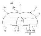
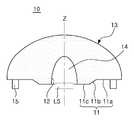
도 5 및 도 6을 참조하여 본 발명의 다른 실시 형태에 따른 발광소자 패키지용 렌즈를 설명한다. 도 5는 본 발명의 다른 실시 형태에 따른 발광소자 패키지용 렌즈를 개략적으로 나타내는 단면도이고, 도 6은 도 5에서 돌출부를 개략적으로 나타내는 확대사시도이다.
A lens for a light emitting device package according to another embodiment of the present invention will be described with reference to FIGS. 5 and 6. FIG. FIG. 5 is a cross-sectional view schematically showing a lens for a light emitting device package according to another embodiment of the present invention, and FIG. 6 is an enlarged perspective view schematically showing a protrusion in FIG.
도 5 및 도 6에서 도시하는 실시 형태에 따른 렌즈(20)를 구성하는 구조는 상기 도 1 내지 도 4에 도시된 실시 형태와 기본적인 구조는 실질적으로 동일하다. 다만, 바닥면(21)의 구조가 상기 도 1 내지 도 4에 도시된 실시 형태와 다르기 때문에 이하에서는 앞서 설명한 실시 형태와 중복되는 부분에 관한 설명은 생략하고 바닥면(21)의 구조를 위주로 설명한다.
The structure of the
도 5 및 도 6을 참조하면, 본 실시 형태에 따른 발광소자 패키지용 렌즈(20)는 상기 광원(LS) 상에 배치되는 바닥면(21)과, 상기 광원(LS)의 광이 입사되는 입사면(22)과, 상기 광이 외부로 방출되는 출사면(23)과, 상기 바닥면(21)에 구비되는 돌출부(24)를 포함할 수 있다.
5 and 6, the
상기 바닥면(21)은 상기 광원(LS)과 마주하는 면이며, 원 형상의 수평 단면 구조를 가질 수 있다. 상기 광원(LS)의 광축(Z)이 지나는 상기 바닥면(21)의 중앙에는 광출사 방향으로 함몰된 홈부(26)가 구비될 수 있다.
The
상기 홈부(26)는 상기 렌즈(20)의 중심을 지나는 광축(Z)에 대해 회전 대칭을 이루는 구조를 가지며, 그 표면은 상기 광원(LS)의 광이 입사되는 입사면(22)으로 정의될 수 있다. 상기 홈부(26)는 상기 바닥면(21)을 통해 외부로 개방되며, 상기 광원(LS)의 상부에서 상기 광원(LS)과 마주하도록 배치될 수 있다.
The
상기 출사면(23)은 상기 입사면(22)을 통해 상기 렌즈(20) 내부로 들어온 광이 외부로 방출되는 면으로 상기 렌즈(20)의 상면에 해당된다. 상기 출사면(23)은 상기 바닥면(21)과 연결되는 테두리로부터 상부 방향(광출사 방향)으로 돌출되는 구조를 가질 수 있다. 상기 출사면(23)은 상기 도 2의 출사면(13)과 동일한 구조를 가질 수 있으며, 이에 대한 구체적인 설명은 생략한다.
The
상기 돌출부(24)는 상기 바닥면(21)의 상기 홈부(26) 둘레를 따라 구비되며, 상기 광원(LS)을 향해 돌출되어 상기 바닥면(21)과 단차를 이룰 수 있다. 상기 돌출부(24)는 상기 바닥면(21) 중 상기 홈부(26)에 인접한 일부 영역에서 상기 홈부(26)를 둘러싸는 구조로 돌출되어 구비될 수 있다.The
상기 돌출부(24)는 관통홀(24a)이 형성된 링 형상을 가지며, 상기 관통홀(24a)의 내측면은 상기 입사면(22)과 연속하는 구조로 연결될 수 있다. 따라서, 상기 입사면(22)은 상기 돌출부(24)에 의해 상기 바닥면(21)에서 더 연장되어 상기 돌출부(24)의 바닥면까지 연장되는 구조를 가질 수 있다. 즉, 상기 입사면(22)은 상기 홈부(26)의 표면과 상기 관통홀(24a)의 내측면을 포함하여 일체로 연결된 면으로 정의될 수 있다.
The protruding
상기 돌출부(24)는 상기 렌즈(20)와 동일한 재질로 이루어질 수 있다. 그리고, 접착제 등을 통해 상기 바닥면(21)에 부착될 수 있다.The
한편, 상기 돌출부(24)의 표면에는 광 산란을 위한 요철 구조가 형성될 수 있다. 이러한 요철 구조는, 예를 들어, 돌출부(24)의 표면을 부식처리하는 방식으로 형성할 수 있다.
On the other hand, a convex-concave structure for light scattering may be formed on the surface of the
상기 돌출부(24)에 인접하여 상기 바닥면(21)에는 지지부(25)가 더 구비될 수 있다. 상기 지지부(25)는 상기 렌즈(20)가 예를 들어 기판 상에 장착되는 경우 상기 렌즈(20)를 고정 및 지지할 수 있다. 즉, 상기 렌즈(20)는 상기 지지부(25)를 통해 상기 기판 상에 장착될 수 있다.A supporting
상기 지지부(25)는 상기 돌출부(24)보다 상기 광원(LS)으로 더 돌출될 수 있다. 따라서, 상기 돌출부(24)는 상기 광원(LS) 상에 위치하고, 상기 입사면(22)은 상기 광원(LS)과 마주하도록 배치될 수 있다.
The
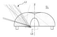
도 7a 및 도 7b에서는 비교예에 따른 렌즈와 본 실시 형태에 따른 렌즈에서의 광 경로를 개략적으로 나타내고 있으며, 도 8a 및 도 8b에서는 각 렌즈에 의해 확산된 광 분포의 그래프를 나타내고 있다.
Figs. 7A and 7B schematically show the optical paths in the lens according to the comparative example and the lens according to the present embodiment, and Figs. 8A and 8B show graphs of the light distribution diffused by each lens.
광원의 광을 확산시켜 넓은 지향각을 구현하는 광(廣)지향각 렌즈는 굴절을 이용하여 중심부에서 광을 측방향의 넓은 영역으로 확산시키는데, 이때 균일한 분포로 광을 확산시키는 것이 중요하다.
A wide diagonal lens that diffuses the light of a light source to realize a wide divergence angle diffuses the light from a central portion to a wide divergent region using refraction. It is important to diffuse the light with a uniform distribution at this time.
도 7a에서와 같이, 바닥면이 평평한 구조를 가지는 비교예에 따른 렌즈(CL)에서는 광원(LS)에서 방출되는 광 중 광원(LS)의 최외곽에서의 광(L1)이 렌즈의 바닥면으로 입사하게 되어 바닥면이 부분적으로 입사면 기능을 하게 된다. 이 경우, 바닥면으로 입사된 광(L1)은 당초 설계된 광 경로를 따라 테두리 방향으로 진행하여 넓게 확산되지 못하고 바닥면에서 굴절되어 중심부 방향으로 진행하게 된다.7A, in the lens CL according to the comparative example having a flat bottom surface, the light L1 at the outermost portion of the light source LS among the light emitted from the light source LS, So that the bottom surface partially functions as an incident surface. In this case, the light L1 incident on the bottom surface proceeds along the designed optical path in the frame direction, is not diffused widely, is refracted at the bottom surface, and proceeds toward the center.
그리고, 도 8a에서와 같이, 바닥면에서 굴절된 광(L1)에 의해 대략 15° 내지 40° 사이의 범위에서 광 분포가 광축에 해당하는 0°에 비해 현저하게 증가하는 모습을 확인할 수 있다. 이에 따라서, 전체적인 광 분포의 균일도가 낮음을 확인할 수 있다. 이러한 불균일한 광 분포는 조명 장치나 디스플레이 장치에서 휘도 저하 및 무라(mura)와 같은 색 얼룩 불량을 유발하는 원인이 될 수 있다.
As shown in FIG. 8A, it can be seen that the light distribution in the range of approximately 15 to 40 degrees by the light L1 refracted from the bottom surface remarkably increases compared with 0 degrees corresponding to the optical axis. Accordingly, it is confirmed that the uniformity of the overall light distribution is low. Such non-uniform light distribution may cause poor luminance and poor color uniformity such as mura in a lighting device or a display device.
한편, 도 7b에서와 같이, 본 실시 형태에 따른 렌즈(10)에서는 바닥면(11)으로부터 부분적으로 돌출된 돌출 구조물에 의해 입사면(12)이 바닥면(11)보다 광원(LS)을 향해 더 연장되는 구조를 가지게 된다. 따라서, 상술한 비교예와 달리 광원(LS)의 최외곽에서의 광(L2)은 모두 입사면(12)을 통해 입사되어 당초 설계된 광 경로를 따라 테두리 방향으로 진행하여 넓게 확산될 수 있다.7B, in the
이에 따라, 도 8b에서와 같이, 광축에서 광 분포가 가장 높고, 광축에서 멀어질수록 대칭을 이루며 감소하는 것을 확인할 수 있다. 따라서, 상기 도 8a에서와 달리 광 분포의 균일도가 현저히 높음을 확인할 수 있다.
Accordingly, as shown in FIG. 8B, it can be seen that the light distribution is the highest at the optical axis, and decreases symmetrically with distance from the optical axis. Therefore, unlike FIG. 8A, the uniformity of light distribution is remarkably high.
도 9를 참조하여 본 발명의 일 실시 형태에 따른 광원 모듈을 설명한다. 도 9는 본 발명의 일 실시 형태에 따른 광원 모듈을 개략적으로 나타내는 단면도이다.
A light source module according to an embodiment of the present invention will be described with reference to FIG. 9 is a cross-sectional view schematically showing a light source module according to an embodiment of the present invention.
도 9를 참조하면, 본 발명의 일 실시 형태에 따른 광원 모듈(100)은 발광소자(30), 상기 발광소자(30)가 실장되는 기판(40) 및 상기 기판(40) 상에 실장되며 상기 발광소자(30) 상에 배치되는 렌즈(10)를 포함하여 구성될 수 있다.
9, a
발광소자(30)는 외부에서 인가되는 구동 전원에 의해 소정 파장의 광을 발생시키는 광전소자일 수 있다. 예를 들어, n형 반도체층 및 p형 반도체층과 이들 사이에 배치된 활성층을 갖는 반도체 발광다이오드(LED) 칩 또는 이를 구비한 패키지를 포함할 수 있다.The
상기 발광소자(30)는 함유되는 물질 또는 형광체와의 조합에 따라서 청색 광, 녹색 광 또는 적색 광을 발광할 수 있으며, 백색 광, 자외 광 등을 발광할 수도 있다.
The
도 10a에서 도시하는 바와 같이, 상기 발광소자(30)는 반사컵(321)을 갖는 몸체(320) 내에 LED 칩(310)이 실장된 패키지 구조를 가질 수 있다.
10A, the
상기 몸체(320)는 상기 LED 칩(310)이 실장되어 지지되는 베이스 부재에 해당하며, 광 반사율이 높은 백색 성형 복합재(molding compound)로 이루어질 수 있다. 이는 LED 칩(110)에서 방출되는 광을 반사시켜 외부로 방출되는 광량을 증가시키는 효과가 있다. 이러한 백색 성형 복합재는 고 내열성의 열경화성 수지 계열 또는 실리콘 수지 계열을 포함할 수 있다. 또한, 열 가소성 수지 계열에 백색 안료 및 충진제, 경화제, 이형제, 산화방지제, 접착력 향상제 등이 첨가될 수 있다. 또한, FR-4, CEM-3, 에폭시 재질 또는 세라믹 재질 등으로도 이루어질 수 있다. 또한, 알루미늄(Al)과 같은 금속 재질로 이루어지는 것도 가능하다.
The
상기 몸체(320)에는 외부 전원과의 전기적 연결을 위한 리드 프레임(322)이 구비될 수 있다. 상기 리드 프레임(322)은 전기 전도성이 우수한 재질, 예를 들어, 알루미늄, 구리 등의 금속 재질로 이루어질 수 있다. 만일, 상기 몸체(320)가 금속 재질로 이루어지는 경우에는 상기 몸체(320)와 상기 리드 프레임(322) 사이에는 절연 물질이 개재될 수 있다.
The
상기 몸체(320)에 구비되는 상기 반사컵(321)은 상기 LED 칩(310)이 실장되는 바닥면으로 상기 리드 프레임(322)이 노출될 수 있다. 그리고, 상기 LED 칩(310)은 상기 노출된 리드 프레임(322)과 전기적으로 접속될 수 있다.The
상기 반사컵(321)의 상기 몸체(320)의 상면으로 노출되는 단면의 크기는 상기 반사컵(321)의 바닥면의 크기보다 큰 구조를 가질 수 있다. 여기서, 상기 반사컵(321)의 상기 몸체(320)의 상면으로 노출되는 단면은 상기 발광소자(30)의 발광면을 정의할 수 있다.
The size of the cross section of the
한편, 상기 LED 칩(310)은 상기 몸체(320)의 반사컵(321) 내에 형성되는 봉지재(330)에 의해 밀봉될 수 있다. 상기 봉지재(330)에는 파장변환물질이 함유될 수 있다.Meanwhile, the
파장변환물질로는, 예컨대 상기 LED 칩(110)에서 발생된 광에 의해 여기되어 다른 파장의 광을 방출하는 형광체가 적어도 1종 이상 함유될 수 있다. 이를 통해 백색 광을 비롯해 다양한 색상의 광이 방출될 수 있도록 조절할 수 있다.As the wavelength converting material, for example, at least one fluorescent material that is excited by the light emitted from the LED chip 110 and emits light of a different wavelength may be contained. This can be adjusted to emit light of various colors including white light.
예를 들어, LED 칩(310)이 청색 광을 발광하는 경우, 황색, 녹색, 적색 또는 오랜지색의 형광체를 조합하여 백색 광을 발광하도록 할 수 있다. 또한, 보라색, 청색, 녹색, 적색 또는 적외선을 발광하는 발광소자 중 적어도 하나를 포함하게 구성할 수도 있다. 이 경우, LED 칩(310)은 연색성(CRI)을 나트륨(Na)등(연색지수 40)에서 태양광(연색지수 100) 수준으로 조절할 수 있으며, 또한, 색온도를 2000K에서 20000K 수준으로 다양한 백색 광을 발생시킬 수 있다. 또한, 필요에 따라서는 보라색, 청색, 녹색, 적색, 오랜지색의 가시광 또는 적외선을 발생시켜 주위 분위기 또는 기분에 맞게 색을 조정할 수 있다. 또한, 식물 성장을 촉진할 수 있는 특수 파장의 광을 발생시킬 수도 있다.For example, when the
상기 청색 LED에 황색, 녹색, 적색 형광체 및/또는 녹색, 적색 LED의 조합으로 만들어지는 백색 광은 2개 이상의 피크 파장을 가지며, 도 11에서 도시하는 CIE 1931 좌표계의 (x, y) 좌표가 (0.4476, 0.4074), (0.3484, 0.3516), (0.3101, 0.3162), (0.3128, 0.3292), (0.3333, 0.3333)을 잇는 선분 상에 위치할 수 있다. 또는, 상기 선분과 흑체 복사 스펙트럼으로 둘러싸인 영역에 위치할 수 있다. 상기 백색 광의 색 온도는 2000K ~ 20000K사이에 해당한다.
(X, y) coordinates of the CIE 1931 coordinate system shown in FIG. 11 have a peak wavelength of ((x, y)) in FIG. 11, and a white light formed by combining the blue LED with a combination of yellow, green and red phosphors and / 0.3476, 0.4074), (0.3484, 0.3516), (0.3101, 0.3162), (0.3128, 0.3292), (0.3333, 0.3333). Alternatively, it may be located in an area surrounded by the line segment and the blackbody radiation spectrum. The color temperature of the white light corresponds to between 2000K and 20000K.
형광체는 다음과 같은 조성식 및 컬러(color)를 가질 수 있다.The phosphor may have the following composition formula and color.
산화물계: 황색 및 녹색 Y3Al5O12:Ce, Tb3Al5O12:Ce, Lu3Al5O12:CeOxide system: yellow and green Y3 Al5 O12 : Ce, Tb3 Al5 O12 : Ce, Lu3 Al5 O12 : Ce
실리케이트계: 황색 및 녹색 (Ba,Sr)2SiO4:Eu, 황색 및 등색 (Ba,Sr)3SiO5:Ce(Ba, Sr)2 SiO4 : Eu, yellow and orange (Ba, Sr)3 SiO5 : Ce
질화물계: 녹색 β-SiAlON:Eu, 황색 La3Si6N11:Ce, 등색 α-SiAlON:Eu, 적색 CaAlSiN3:Eu, Sr2Si5N8:Eu, SrSiAl4N7:EuThe nitride-based: the green β-SiAlON: Eu, yellowLa 3 Si 6 N 11: Ce , orange-colored α-SiAlON: Eu, redCaAlSiN 3: Eu, Sr 2 Si 5 N 8: Eu, SrSiAl 4 N 7: Eu
플루오라이트(fluoride)계: KSF계 적색 K2SiF6:Mn4+
Fluoride system: KSF system Red K2 SiF6 : Mn 4 +
형광체 조성은 기본적으로 화학양론(Stoichiometry)에 부합하여야 하며, 각 원소들은 주기율표상 각 족들 내 다른 원소로 치환이 가능하다. 예를 들어 Sr은 알카리토류(II)족의 Ba, Ca, Mg 등으로, Y는 란탄계열의 Tb, Lu, Sc, Gd 등으로 치환이 가능하다. 또한, 활성제인 Eu 등은 원하는 에너지 준위에 따라 Ce, Tb, Pr, Er, Yb 등으로 치환이 가능하며, 활성제 단독 또는 특성 변형을 위해 부활성제 등이 추가로 적용될 수 있다.The phosphor composition should basically conform to the stoichiometry, and each element can be replaced with another element in each group on the periodic table. For example, Sr can be substituted with Ba, Ca, Mg, etc. of the alkaline earth (II) group, and Y can be replaced with lanthanide series Tb, Lu, Sc, Gd and the like. In addition, Eu, which is an activator, can be substituted with Ce, Tb, Pr, Er, Yb or the like according to a desired energy level.
또한, 형광체 대체 물질로 양자점(Quantum Dot, QD) 등의 물질들이 적용될 수 있으며, 형광체와 QD를 혼합 또는 단독으로 사용될 수 있다.In addition, materials such as quantum dots (QD) can be applied as a substitute for a fluorescent material, and the fluorescent material and QD can be mixed or used alone.
QD는 CdSe, InP 등의 코어(Core)(3~10nm)와 ZnS, ZnSe 등의 셀(Shell)(0.5 ~ 2nm) 및 Core, Shell의 안정화를 위한 리간드(ligand)의 구조로 구성될 수 있으며, 사이즈에 따라 다양한 컬러를 구현할 수 있다.
QD can be composed of a core (3 to 10 nm) such as CdSe and InP, a shell (0.5 to 2 nm) such as ZnS and ZnSe, and a ligand for stabilizing core and shell , And various colors can be implemented depending on the size.
본 실시 형태에서는 상기 발광소자(30)가 LED 칩(310)이 반사컵(321)을 갖는 몸체(320) 내부에 구비된 패키지 구조인 것을 예시하고 있으나, 이에 한정하는 것은 아니다. 도 10b에서와 같이, 상기 발광소자(30')는 상기 LED 칩(310')이 상기 몸체(320')의 상면에 실장된 칩온보드(COB) 구조일 수 있다. 이 경우, 상기 몸체(320')는 회로배선이 형성된 회로기판일 수 있으며, 상기 봉지재(330')는 상기 몸체(320')의 상면 상에 돌출되어 상기 LED 칩(310')을 덮는 렌즈 구조로 구비될 수 있다.In the present embodiment, the
또한, 본 실시 형태에서는 상기 발광소자(30)가 패키지 단품인 것을 예시하고 있으나, 이에 한정하는 것은 아니다. 예를 들어, 상기 발광소자(30)는 상기 LED 칩(310) 자체일 수도 있다.
In this embodiment, the
기판(40)은 FR4 타입의 인쇄회로기판(PCB) 혹은 변형이 쉬운 플렉서블(flexible) 인쇄회로기판일 수 있고, 에폭시, 트리아진, 실리콘, 및 폴리이미드 등을 함유하는 유기 수지 소재 및 기타 유기 수지 소재로 형성될 수 있다. 또한, 실리콘 나이트라이드, AlN, Al2O3 등의 세라믹 소재로 형성되거나, MCPCB, MCCL 등과 같이 금속 및 금속화합물을 소재로 하여 형성될 수 있다.The
상기 기판(40)에는 상기 발광소자(30)와 전기적으로 접속되는 회로 배선(41)이 구비될 수 있다.
The
렌즈(10)는 상기 도 1 내지 도 6에서 개시하는 렌즈와 실질적으로 동일하며, 따라서 이에 대한 설명은 생략한다.
The
본 실시 형태에서는 상기 광원 모듈(100)이 기판(40) 상에 실장된 단일의 발광소자(30)와 단일의 렌즈(10)로 구성되는 것으로 예시하고 있으나, 이에 한정하는 것은 아니다. 예를 들어, 상기 발광소자(30)는 복수개로 구비되어 상기 기판(40) 상에 배열될 수 있으며, 상기 렌즈(10)는 상기 발광소자(30)에 대응하여 복수개로 구비되며, 각 발광소자(30) 상에 배치될 수 있다.
In the present embodiment, the
도 12 내지 도 14를 참조하여 발광소자에 채용될 수 있는 LED 칩의 다양한 실시예를 설명한다. 도 12 내지 도 14는 본 발명의 일 실시 형태에 따른 발광소자에 채용될 수 있는 발광다이오드 칩의 다양한 예를 나타내는 단면도이다.
Various embodiments of the LED chip that can be employed in the light emitting device will be described with reference to Figs. 12 to 14. Fig. 12 to 14 are sectional views showing various examples of light emitting diode chips that can be employed in a light emitting device according to an embodiment of the present invention.
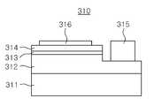
도 12를 참조하면, LED 칩(310)은 성장 기판(311)상에 순차적으로 적층된 제1 도전형 반도체층(312), 활성층(313) 및 제2 도전형 반도체층(314)을 포함할 수 있다.
12, the
성장 기판(311) 상에 적층되는 제1 도전형 반도체층(312)은 n형 불순물이 도핑된 n형 질화물 반도체층일 수 있다. 그리고, 제2 도전형 반도체층(314)은 p형 불순물이 도핑된 p형 질화물 반도체층일 수 있다. 다만, 실시 형태에 따라서 제1 및 제2 도전형 반도체층(312, 314)은 위치가 바뀌어 적층될 수도 있다. 이러한 제1 및 제2 도전형 반도체층(312, 314)은 AlxInyGa(1-x-y)N 조성식(여기서, 0≤x<1, 0≤y<1, 0≤x+y<1)을 가지며, 예컨대, GaN, AlGaN, InGaN, AlInGaN 등의 물질이 이에 해당될 수 있다.
The first
제1 및 제2 도전형 반도체층(312, 314) 사이에 배치되는 활성층(313)은 전자와 정공의 재결합에 의해 소정의 에너지를 갖는 광을 방출한다. 활성층(313)은 제1 및 제2 도전형 반도체층(312, 314)의 에너지 밴드 갭보다 작은 에너지 밴드 갭을 갖는 물질을 포함할 수 있다. 예를 들어, 제1 및 제2 도전형 반도체층(312, 314)이 GaN계 화합물 반도체인 경우, 활성층(313)은 GaN의 에너지 밴드 갭보다 작은 에너지 밴드 갭을 갖는 InGaN계 화합물 반도체를 포함할 수 있다. 또한, 활성층(313)은 양자우물층과 양자장벽층이 서로 교대로 적층된 다중 양자우물(Multiple Quantum Wells, MQW) 구조, 예컨대, InGaN/GaN 구조가 사용될 수도 있다. 다만, 이에 제한되는 것은 아니므로 상기 활성층(313)은 단일 양자우물 구조(Single Quantum Well, SQW)가 사용될 수도 있다.
The
상기 LED 칩(310)은 상기 제1 및 제2 도전형 반도체층(312, 314)과 각각 전기적으로 접속하는 제1 및 제2 전극 패드(315, 316)를 구비할 수 있다. 상기 제1 및 제2 전극 패드(315, 316)는 동일한 방향을 향하도록 노출 및 배치될 수 있다. 그리고, 와이어 본딩 또는 플립 칩 본딩 방식으로 기판과 전기적으로 접속될 수 있다.
The
도 13에 도시된 LED 칩(410)은 성장 기판(411) 상에 형성된 반도체 적층체를 포함한다. 상기 반도체 적층체는 제1 도전형 반도체층(412), 활성층(413) 및 제2 도전형 반도체층(414)을 포함할 수 있다.The
상기 LED 칩(410)은 상기 제1 및 제2 도전형 반도체층(412, 414)에 각각 접속된 제1 및 제2 전극 패드(415, 416)를 포함한다. 상기 제1 전극 패드(415)는 제2 도전형 반도체층(414) 및 활성층(413)을 관통하여 제1 도전형 반도체층(412)과 접속된 도전성 비아(415a) 및 도전성 비아(415a)에 연결된 전극 연장부(415b)를 포함할 수 있다. 도전성 비아(415a)는 절연층(417)에 의해 둘러싸여 활성층(413) 및 제2 도전형 반도체층(414)과 전기적으로 분리될 수 있다. 도전성 비아(415a)는 반도체 적층체가 식각된 영역에 배치될 수 있다. 도전성 비아(415a)는 접촉 저항이 낮아지도록 개수, 형상, 피치 또는 제1 도전형 반도체층(412)과의 접촉 면적 등을 적절히 설계할 수 있다. 또한, 도전성 비아(415a)는 반도체 적층체 상에 행과 열을 이루도록 배열됨으로써 전류 흐름을 개선시킬 수 있다. 상기 제2 전극 패드(416)는 제2 도전형 반도체층(414) 상의 오믹 콘택층(416a) 및 전극 연장부(416b)를 포함할 수 있다.
The
도 14에 도시된 LED 칩(510)은 성장 기판(511)과, 상기 성장 기판(511) 상에 형성된 제1 도전형 베이스층(512)과, 상기 제1 도전형 베이스층(512) 상에 형성된 복수의 나노 발광구조물(513)을 포함한다. 그리고, 절연층(514) 및 충진부(517)를 더 포함할 수 있다.The
나노 발광구조물(513)은 제1 도전형 반도체 코어(513a)와 그 코어(513a)의 표면에 셀층으로 순차적으로 형성된 활성층(513b) 및 제2 도전형 반도체층(513c)을 포함한다.The nano-light emitting structure 513 includes a first conductivity
본 실시예에서, 나노 발광구조물(513)은 코어-셀(core-shell) 구조로서 예시되어 있으나, 이에 한정되지 않고 피라미드 구조와 같은 다른 구조를 가질 수 있다. 상기 제1 도전형 반도체 베이스층(512)은 나노 발광구조물(513)의 성장면을 제공하는 층일 수 있다. 상기 절연층(514)은 나노 발광구조물(513)의 성장을 위한 오픈 영역을 제공하며, SiO2 또는 SiNx와 같은 유전체 물질일 수 있다. 상기 충진부(517)는 나노 발광구조물(513)을 구조적으로 안정화시킬 수 있으며, 빛을 투과 또는 반사하는 역할을 수행할 수 있다. 이와 달리, 상기 충진부(517)가 투광성 물질을 포함하는 경우, 충진부(517)는 SiO2,SiNx, 탄성 수지, 실리콘(silicone), 에폭시 수지, 고분자 또는 플라스틱과 같은 투명한 물질로 형성될 수 있다. 필요에 따라, 상기 충진부(517)가 반사성 물질을 포함하는 경우, 충진부(517)는 PPA(polypthalamide) 등의 고분자 물질에 고반사성을 가진 금속분말 또는 세라믹 분말이 사용될 수 있다. 고반사성 세라믹 분말로서는, TiO2, Al2O3, Nb2O5, Al2O3 및 ZnO로 구성된 그룹으로부터 선택된 적어도 하나일 수 있다. 이와 달리, 고반사성 금속이 사용될 수도 있으며, Al 또는 Ag와 같은 금속일 수 있다.In this embodiment, the nano-light-emitting structure 513 is illustrated as a core-shell structure, but it is not limited thereto and may have another structure such as a pyramid structure. The first conductive
상기 제1 및 제2 전극 패드(515, 516)는 나노 발광구조물(513)의 하면에 배치될 수 있다. 상기 제1 전극 패드(515)는 제1 도전형 반도체 베이스층(512)의 노출된 상면에 위치하고, 제2 전극 패드(516)는 나노 발광구조물(513) 및 충진부(517)의 하부에 형성되는 오믹 콘택층(516a) 및 전극 연장부(516b)를 포함한다. 이와 달리, 오믹 콘택층(516a)과 전극 연장부(516b)는 일체로 형성될 수도 있다.
The first and
도 15 내지 도 17을 참조하여 본 발명의 광원 모듈을 채용하는 다양한 실시 형태에 따른 조명 장치를 설명한다.
15 to 17, a lighting apparatus according to various embodiments employing the light source module of the present invention will be described.
도 15에서는 본 발명의 일 실시 형태에 따른 조명 장치를 개략적으로 나타내고 있다.Fig. 15 schematically shows a lighting apparatus according to an embodiment of the present invention.
도 15를 참조하면, 본 발명의 일 실시 형태에 따른 조명 장치(1000)는 벌브형 램프일 수 있으며, 실내 조명용, 예를 들어, 다운라이트(downlight)로 사용될 수 있다. 조명 장치(1000)는 전기 연결 구조(1030)를 갖는 하우징(1020)과 상기 하우징(1020)에 장착되는 적어도 하나의 광원 모듈(1010)을 포함하여 구성될 수 있다. 그리고, 상기 하우징(1020)에 장착되어 상기 적어도 하나의 광원 모듈(1010)을 덮는 커버(1040)를 더 포함할 수 있다.
Referring to FIG. 15, the
상기 광원 모듈(1010)은 상기 도 9의 광원 모듈(100)과 실질적으로 동일하며, 따라서 이에 대한 구체적인 설명은 생략한다. 상기 광원 모듈(1010)은 기판(1011) 상에 복수의 발광소자와 렌즈가 장착되어 배치되는 구성을 가질 수 있다.
The
상기 하우징(1020)은 상기 광원 모듈(1010)을 지지하는 프레임으로서의 기능과, 상기 광원 모듈(1010)에서 발생하는 열을 외부로 방출하는 히트 싱크로서의 기능을 수행할 수 있다. 이를 위해 상기 하우징(1020)은 열전도율이 높고 견고한 재질로 이루어질 수 있으며, 예를 들어, 알루미늄(Al)과 같은 금속 재질, 방열 수지등으로 이루어질 수 있다.The
하우징(1020)의 외측면에는 공기와의 접촉면적을 증가시켜 방열 효율이 향상되도록 하기 위한 복수의 방열핀(1021)이 구비될 수 있다.
The outer surface of the
상기 하우징(1020)에는 상기 광원 모듈(1010)과 전기적으로 연결되는 전기 연결 구조(1030)가 구비된다. 상기 전기 연결 구조(1030)는 단자부(1031)와, 상기 단자부(1031)를 통해 공급되는 구동 전원을 상기 광원 모듈(1010)로 공급하는 구동부(1032)를 포함할 수 있다.The
상기 단자부(1031)는 조명 장치(1000)를, 예컨대 소켓 등에 장착하여 고정 및 전기적으로 연결될 수 있도록 한다. 본 실시 형태에서는 단자부(1031)가 슬라이딩 삽입되는 핀 타입의 구조를 가지는 것으로 예시하고 있으나, 이에 한정하는 것은 아니다. 필요에 따라서 상기 단자부(1031)는 나사산을 가져 돌려서 끼워지는 에디슨 타입의 구조를 가지는 것도 가능하다.
The
상기 구동부(1032)는 외부의 구동 전원을 상기 광원 모듈을 구동시킬 수 있는 적정한 전류원으로 변환시켜 제공하는 역할을 한다. 이러한 구동부(1032)는, 예를 들어 AC-DC 컨버터, 정류회로 부품, 퓨즈 등으로 구성될 수 있다. 또한, 경우에 따라 원격 제어를 구현할 수 있는 통신 모듈을 더 포함할 수도 있다.
The
상기 커버(1040)는 상기 하우징(1020)에 장착되어 상기 적어도 하나의 광원 모듈(1010)을 덮으며, 볼록한 렌즈 형상 또는 벌브 형상을 가질 수 있다. 상기 커버(1040)는 광 투과성 재질로 이루어질 수 있으며, 광 분산물질을 함유할 수 있다.
The
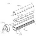
도 16은 본 발명의 다른 실시 형태에 따른 조명 장치를 개략적으로 나타내는 분해사시도이다. 도 16을 참조하면, 조명 장치(1100)는 일 예로서 바(bar) 타입 램프일 수 있으며, 광원 모듈(1110), 하우징(1120), 단자(1130) 및 커버(1140)를 포함하여 구성될 수 있다.
16 is an exploded perspective view schematically showing a lighting apparatus according to another embodiment of the present invention. 16, the
광원 모듈(1110)은 상기 도 9의 광원 모듈이 채용될 수 있다. 따라서, 이에 대한 구체적인 설명은 생략한다. 상기 광원 모듈(1110)은 기판(1111) 상에 복수의 발광소자와 렌즈가 장착되어 기판(1111)을 따라 배열되는 구성을 가질 수 있다.
The
하우징(1120)은 일면(1122)에 상기 광원 모듈(1110)을 탑재하여 고정시킬 수 있으며, 상기 광원 모듈(1110)에서 발생되는 열을 외부로 방출시킬 수 있다. 이를 위해 상기 하우징(1120)은 열전도율이 우수한 재질, 예컨대 금속 재질로 이루어질 수 있으며, 양 측면에는 방열을 위한 복수의 방열 핀(1121)이 돌출되어 형성될 수 있다.The
상기 하우징(1120)의 일면(1122)에는 상기 광원 모듈(1110)이 장착될 수 있다.
The
커버(1140)는 광원 모듈(1110)을 덮을 수 있도록 하우징(1120)의 걸림 홈(1123)에 체결된다. 그리고, 상기 광원 모듈(1110)에서 발생된 광이 외부로 전체적으로 균일하게 조사될 수 있도록 반원 형태의 곡면을 가질 수 있다. 커버(1140)의 바닥면에는 하우징(1120)의 걸림 홈(1123)에 맞물리는 돌기(1141)가 길이 방향을 따라서 형성될 수 있다.
The
단자(1130)는 하우징(1120)의 길이 방향의 양 끝단부 중 개방된 적어도 일측에 구비되어 광원 모듈(1110)에 전원을 공급할 수 있으며, 외부로 돌출된 전극 핀(1133)을 포함할 수 있다.
The terminal 1130 may include at least one open end of the lengthwise ends of the
도 17은 본 발명의 다른 실시 형태에 따른 조명 장치를 개략적으로 나타내는 분해사시도이다. 도 17을 참조하면, 조명 장치(1200)는 일 예로서 면 광원 타입의 구조를 가질 수 있으며, 광원 모듈(1210), 하우징(1220), 커버(1240) 및 히트 싱크(1250)를 포함하여 구성될 수 있다.
17 is an exploded perspective view schematically showing a lighting apparatus according to another embodiment of the present invention. 17, the
광원 모듈(1210)은 상기 도 9의 광원 모듈이 채용될 수 있다. 따라서, 이에 대한 구체적인 설명은 생략한다. 상기 광원 모듈(1210)은 기판(1211) 상에 복수의 발광소자와 렌즈가 장착되어 기판(1211)을 따라 배열되는 구성을 가질 수 있다.
The
하우징(1220)은 상기 광원 모듈(1210)이 탑재되는 일면(1222)과 상기 일면(1222) 둘레에서 연장되는 측면(1224)을 포함하여 박스형 구조를 가질 수 있다. 하우징(1220)은 상기 광원 모듈(1210)에서 발생되는 열을 외부로 방출시킬 수 있도록 열전도율이 우수한 재질, 예컨대 금속 재질로 이루어질 수 있다.The
상기 하우징(1220)의 일면(1222)에는 추후 설명하는 히트 싱크(1250)가 삽입되어 체결되는 홀(1226)이 상기 일면(1222)을 관통하여 형성될 수 있다. 그리고, 상기 일면(1222)에 탑재되는 상기 광원 모듈(1210)의 기판(1211)은 부분적으로 상기 홀(1226)상에 걸쳐져서 외부로 노출될 수 있다.
A
커버(1240)는 상기 광원 모듈(1210)을 덮을 수 있도록 상기 하우징(1220)에 체결될 수 있다. 그리고, 전체적으로 편평한 구조를 가질 수 있다.
The
히트 싱크(1250)는 하우징(1220)의 타면(1225)을 통해 상기 홀(1226)에 체결될 수 있다. 그리고, 상기 홀(1226)을 통해 상기 광원 모듈(1210)과 접촉하여 상기 광원 모듈(1210)의 열을 외부로 방출할 수 있다. 방열 효율의 향상을 위해 상기 히트 싱크(1250)는 복수의 방열 핀(1251)을 구비할 수 있다. 상기 히트 싱크(1250)는 상기 하우징(1220)과 같이 열전도율이 우수한 재질로 이루어질 수 있다.
The
발광소자를 이용한 조명 장치는 그 용도에 따라 크게 실내용(indoor) 과 실외용(outdoor)으로 구분될 수 있다. 실내용 LED 조명 장치는 주로 기존 조명 대체용(Retrofit)으로 벌브형 램프, 형광등(LED-tube), 평판형 조명 장치가 여기에 해당되며, 실외용 LED 조명 장치는 가로등, 보안등, 투광등, 경관등, 신호등 등이 해당된다.The lighting device using the light emitting device can be largely divided into indoor and outdoor depending on its use. Indoor LED lighting devices are mainly retrofit, bulb type lamps, fluorescent lamps (LED-tubes) and flat type lighting devices. Outdoor LED lighting devices are street lamps, security lamps, Etc., and traffic lights.
또한, LED를 이용한 조명 장치는 차량용 내외부 광원으로 활용 가능하다. 내부 광원으로는 차량용 실내등, 독서등, 계기판의 각종 광원등으로 사용 가능하며, 차량용 외부 광원으로 전조등, 브레이크등, 방향지시등, 안개등, 주행등 등 모든 광원에 사용 가능하다.Further, the illumination device using the LED can be utilized as an internal and external light source for a vehicle. As an internal light source, it can be used as a vehicle interior light, a reading light, various light sources of a dashboard, etc. It is an external light source for a vehicle and can be used for all light sources such as headlights, brakes, turn signals, fog lights,
아울러, 로봇 또는 각종 기계 설비에 사용되는 광원으로 LED 조명 장치가 적용될 수 있다. 특히, 특수한 파장대를 이용한 LED 조명은 식물의 성장을 촉진시키고, 감성 조명으로서 사람의 기분을 안정시키거나 병을 치료할 수도 있다.
In addition, an LED lighting device can be applied as a light source used in a robot or various kinds of mechanical equipment. In particular, LED lighting using a special wavelength band can stimulate the growth of plants, emotional lighting can stabilize a person's mood or heal disease.
도 18 내지 도 21을 참조하여 상술한 조명 장치를 채용한 조명 시스템을 설명한다. 본 실시 형태에 따른 조명 시스템(2000)은 주변 환경(예를 들어, 온도 및 습도)에 따라 색온도를 자동적으로 조절 가능하며, 단순한 조명의 역할이 아니라 인간의 감성을 충족시킬 수 있는 감성 조명으로써 조명 장치를 제공할 수 있다.
An illumination system employing the above-described illumination device will be described with reference to Figs. 18 to 21. Fig. The
도 18은 본 발명의 일 실시 형태에 따른 조명 시스템을 개략적으로 나타내는 블록도이다.18 is a block diagram schematically showing an illumination system according to an embodiment of the present invention.
도 18을 참조하면, 본 발명의 일 실시 형태에 따른 조명 시스템(2000)은 센싱부(2010), 제어부(2020), 구동부(2030) 및 조명부(2040)를 포함할 수 있다.18, an
센싱부(2010)는 실내 또는 실외에 설치될 수 있으며, 온도센서(2011) 및 습도센서(2012)를 구비하여 주변의 온도 및 습도 중 적어도 하나의 공기 조건을 측정한다. 그리고, 상기 센싱부(2010)는 전기적으로 접속된 상기 제어부(2020)로 상기 측정한 공기 조건, 즉 온도 및 습도를 전달한다.The
제어부(2020)는 측정된 공기의 온도 및 습도를 사용자에 의해 미리 설정된 공기 조건(온도 및 습도 범위)과 비교하고, 그 비교 결과, 상기 공기 조건에 상응하는 조명부(2040)의 색온도를 결정한다. 상기 제어부(2020)는 상기 구동부(2030)와 전기적으로 접속되며, 상기 결정된 색온도로 상기 조명부(2040)를 구동할 수 있도록 상기 구동부(2030)를 제어한다.
The
조명부(2040)는 상기 구동부(2030)에서 공급하는 전원에 따라 동작한다. 상기 조명부(2040)는 상기 도 15 내지 도 17에서 도시한 조명 장치를 적어도 하나 포함할 수 있다. 예를 들어, 상기 조명부(2040)는 도 19에서 도시하는 바와 같이, 서로 다른 색온도를 갖는 제1 조명 장치(2041) 및 제2 조명 장치(2042)로 구성될 수 있으며, 각 조명 장치(2041, 2042)는 동일한 백색광을 발광하는 복수의 발광소자를 구비할 수 있다.
The
제1 조명 장치(2041)는 제1 색온도의 백색광을 방출하며, 제2 조명 장치(2042)는 제2 색온도의 백색광을 방출하며, 제1 색온도가 제2 색온도보다 낮을 수 있다. 또는, 반대로 제1 색온도가 제2 색온도보다 높을 수도 있다. 여기서, 상대적으로 색온도가 낮은 백색은 따뜻한 백색에 해당하고, 상대적으로 색온도가 높은 백색은 차가운 백색에 해당한다. 이러한 제1 및 제2 조명 장치(2041, 2042)에 전원이 공급되면, 각각 제1 및 제2 색온도를 갖는 백색광을 방출하고, 각 백색광은 서로 혼합되어 제어부(2020)에서 결정된 색온도를 갖는 백색광을 구현할 수 있다.The
구체적으로, 제1 색온도가 제2 색온도보다 낮을 경우, 제어부(2020)에서 결정된 색온도가 상대적으로 높게 결정되면, 제1 조명 장치(2041)의 광량을 감소시키고, 제2 조명 장치(2042)의 광량을 증가시켜 혼합된 백색광이 상기 결정된 색온도가 되도록 구현할 수 있다. 반대로, 결정된 색온도가 상대적으로 낮게 결정되면, 제1 조명 장치(2041)의 광량을 증가시키고, 제2 조명 장치(2042)의 광량을 감소시켜 혼합된 백색광이 상기 결정된 색온도가 되도록 구현할 수 있다. 이때, 각 조명 장치(2041, 2042)의 광량은 전원을 조절하여 전체 발광소자의 광량을 조절하는 것에 의해 구현되거나, 구동되는 발광소자 수를 조절하는 것에 의해 구현될 수 있다.
Specifically, when the first color temperature is lower than the second color temperature, if the color temperature determined by the
도 20은 도 18에 도시된 조명 시스템의 제어방법을 설명하기 위한 순서도이다. 도 20을 참조하면, 먼저 사용자가 제어부(2020)를 통해 온도 및 습도 범위에 따른 색온도를 설정한다(S10). 설정된 온도 및 습도 데이터는 제어부(2020)에 저장된다.
20 is a flowchart for explaining the control method of the illumination system shown in Fig. Referring to FIG. 20, a user sets a color temperature according to a temperature and a humidity range through a control unit 2020 (S10). The set temperature and humidity data is stored in the
일반적으로 색온도가 6000K 이상이면 청색 등의 체감적으로 시원한 느낌의 색상을 연출할 수 있으며, 색온도가 4000K 이하이면, 적색 등의 체감적으로 따뜻한 느낌의 색상을 연출할 수 있다. 따라서, 본 실시 형태에서는 사용자가 제어부(2020)를 통해 온도 및 습도가 20도 및 60%를 넘는 경우, 조명부(2040)의 색온도가 6000K 이상으로 점등되도록 설정하고, 온도 및 습도가 10도 ~ 20도 및 40% ~ 60%인 경우, 조명부(2040)의 색온도가4000 ~ 6000K 사이로 점등되도록 설정하고, 온도 및 습도가 10도 이하 및 40% 이하인 경우, 조명부(2040)의 색온도가 4000K 이하로 점등되도록 설정한다.
In general, when the color temperature is 6000K or more, it can produce a feeling of cool feeling such as blue, and when the color temperature is 4000K or less, it is possible to produce a warm feeling feeling such as red. Therefore, in the present embodiment, when the temperature and the humidity exceed 20% and 60% through the
다음으로, 센싱부(2010)는 주변의 온도 및 습도 중 적어도 하나의 조건을 측정한다(S20). 센싱부(2010)에서 측정된 온도 및 습도는 제어부(2020)로 전달된다.
Next, the
이어서, 제어부(2020)는 센싱부(2010)로부터 전달된 측정값과 설정값을 비교한다(S30). 여기서, 측정값은 센싱부(2010)에서 측정한 온도 및 습도 데이터이며, 설정값은 사용자가 제어부(2020)에 미리 설정하여 저장된 온도 및 습도 데이터이다. 즉, 제어부(2020)는 상기 측정된 온도 및 습도와 미리 설정된 온도 및 습도를 비교한다.
Next, the
비교결과, 측정값이 설정값 범위를 만족하는지 판단한다(S40). 측정값이 설정값 범위를 만족하면 현재 색온도를 유지하고, 다시 온도 및 습도를 측정한다(S20). 한편, 측정값이 설정값 범위를 만족하지 못할 경우, 측정값에 해당하는 설정값을 검출하고, 이에 해당하는 색온도를 결정한다(S50). 그리고, 제어부(2020)는 결정한 색온도로 조명부(2040)가 구동되도록 구동부(2030)를 제어한다.
As a result of the comparison, it is determined whether the measurement value satisfies the set value range (S40). If the measurement value satisfies the set value range, the current color temperature is maintained, and the temperature and humidity are again measured (S20). On the other hand, if the measured value does not satisfy the set value range, the set value corresponding to the measured value is detected and the corresponding color temperature is determined (S50). The
그러면, 구동부(2030)는 상기 결정된 색온도가 되도록 조명부(2040)를 구동한다(S60). 즉, 구동부(10030)는 결정된 색온도를 구동하기 위해 필요한 전원을 조명부(2040)에 공급한다. 이로써, 조명부(2040)는 주변의 온도 및 습도에 따라 사용자가 미리 설정한 온도 및 습도에 해당하는 색온도로 조절될 수 있다.
Then, the
이로써, 조명 시스템은 주변의 온도 및 습도 변화에 따라 자동적으로 실내 조명부의 색온도를 조절할 수 있으며, 이로써 자연 환경 변화에 따라 달라지는 인간의 감성을 충족시킬 수 있고, 또한, 심리적 안정감을 줄 수 있다.
Thus, the illumination system can automatically adjust the color temperature of the indoor lighting unit according to the ambient temperature and humidity change, thereby satisfying the human sensibility that changes according to the change of the natural environment, and also providing the psychological stability feeling.
도 21은 도 18에 도시된 조명 시스템을 개략적으로 구현한 사용 예시도이다. 도 21에 도시된 바와 같이, 조명부(2040)는 실내 조명등으로써 천장에 설치될 수 있다. 이때, 센싱부(2010)는 실외의 외기 온도 및 습도를 측정하기 위해, 별도의 개별 장치로 구현되어 외부 벽에 설치될 수 있다. 그리고, 제어부(2020)는 사용자의 설정 및 확인이 용이하도록 실내에 설치될 수 있다. 하지만, 본 발명의 조명 시스템은 이에 한정되는 것은 아니며, 인테리어 조명을 대신하여 벽에 설치되거나, 스탠드등과 같이 실내외에서 사용할 수 있는 조명등에 모두 적용될 수 있다.
Fig. 21 is an example of a schematic implementation of the illumination system shown in Fig. 18; As shown in FIG. 21, the
LED를 이용한 상술한 조명 장치는 제품 형태, 장소 및 목적에 따라 광학 설계가 변할 수 있다. 예컨대, 상술한 감성 조명과 관련하여 조명의 색, 온도, 밝기 및 색상을 컨트롤하는 기술 외에 스마트폰과 같은 휴대기기를 활용한 무선(원격) 제어 기술을 이용하여 조명을 제어하는 기술을 들 수 있다.The above-described illumination device using LEDs may vary in optical design depending on the product type, place and purpose. For example, in connection with the emotional illumination described above, there is a technique of controlling illumination using a wireless (remote) control technique utilizing a portable device such as a smart phone, in addition to a technique of controlling the color, temperature, brightness, and color of illumination .
또한, 이와 더불어 LED 조명 장치와 디스플레이 장치들에 통신 기능을 부가하여 LED 광원의 고유 목적과 통신 수단으로서의 목적을 동시에 달성하고자 하는 가시광 무선통신 기술도 가능하다. 이는 LED 광원이 기존의 광원들에 비해 수명이 길고 전력 효율이 우수하며 다양한 색 구현이 가능할 뿐만 아니라 디지털 통신을 위한 스위칭 속도가 빠르고 디지털 제어가 가능하다는 장점을 갖고 있기 때문이다.In addition, a visible light wireless communication technology is also available in which a communication function is added to the LED illumination device and the display devices to simultaneously achieve the intrinsic purpose of the LED light source and the purpose of the communication means. This is because the LED light source has a longer lifetime than the conventional light sources, has excellent power efficiency, can realize various colors, and has a fast switching speed for digital communication and digital control.
가시광 무선통신 기술은 인간이 눈으로 인지할 수 있는 가시광 파장 대역의 빛을 이용하여 무선으로 정보를 전달하는 무선통신 기술이다. 이러한 가시광 무선통신 기술은 가시광 파장 대역의 빛을 이용한다는 측면에서 기존의 유선 광통신기술 및 적외선 무선통신과 구별되며, 통신 환경이 무선이라는 측면에서 유선 광통신 기술과 구별된다.The visible light wireless communication technology is a wireless communication technology that wirelessly transmits information using light of a visible light wavelength band that can be perceived by human eyes. Such a visible light wireless communication technology is distinguished from existing wired optical communication technology and infrared wireless communication in that it uses light in a visible light wavelength band and is distinguished from wired optical communication technology in terms of wireless communication environment.
또한, 가시광 무선통신 기술은 RF 무선통신과 달리 주파수 이용 측면에서 규제 또는 허가를 받지 않고 자유롭게 이용할 수 있다는 편리성과 물리적 보안성이 우수하고 통신 링크를 사용자가 눈으로 확인할 수 있다는 차별성을 가지고 있으며, 무엇보다도 광원의 고유 목적과 통신기능을 동시에 얻을 수 있다는 융합 기술로서의 특징을 가지고 있다.
In addition, unlike RF wireless communication, visible light wireless communication technology has the advantage that it can be freely used without being regulated or licensed in terms of frequency utilization, has excellent physical security, and has a difference in that a user can visually confirm a communication link. And has the characteristic of being a convergence technology that can obtain the intrinsic purpose of the light source and the communication function at the same time.
이상에서 본 발명의 실시 형태에 대하여 상세하게 설명하였지만 본 발명의 권리범위는 이에 한정되는 것은 아니고, 청구범위에 기재된 본 발명의 기술적 사상을 벗어나지 않는 범위 내에서 다양한 수정 및 변형이 가능하다는 것은 당 기술분야의 통상의 지식을 가진 자에게는 자명할 것이다.
Although the embodiments of the present invention have been described in detail, it is to be understood that the scope of the present invention is not limited thereto and that various modifications and changes may be made thereto without departing from the scope of the present invention. It will be obvious to those of ordinary skill in the art.
10, 20... 렌즈11, 21... 바닥면
12, 22... 입사면13, 23... 출사면
14, 26... 홈부24... 돌출부
15, 25... 지지부30... 발광소자
40... 기판41... 회로 배선
100... 광원 모듈10, 20 ...
12, 22 ... incident surfaces 13, 23 ... emergent surface
14, 26 ...
15, 25 ...
40 ...
100 ... light source module
Claims (20)
Translated fromKorean상기 바닥면의 중앙에서 상기 바닥면과 연결되며, 광원 상에 배치되어 상기 광원으로부터의 광이 입사하는 입사면; 및
상기 바닥면의 가장자리에서 상기 바닥면과 연결되며, 상기 광이 외부로 방출되는 출사면을 포함하며,
상기 바닥면은 상기 입사면과 연결되는 영역을 포함하는 중앙 영역이 상기 광원을 향하여 부분적으로 돌출된 비평판형 구조를 가지는 것을 특징으로 하는 발광소자 패키지용 렌즈.
Bottom surface;
An incident surface connected to the bottom surface at the center of the bottom surface, the incident surface being disposed on the light source and receiving light from the light source; And
And an emission surface connected to the bottom surface at an edge of the bottom surface and emitting the light to the outside,
Wherein the bottom surface has a non-planar structure in which a central region including an area connected to the incident surface is partially protruded toward the light source.
상기 입사면은 상기 광원의 광축이 지나는 상기 바닥면의 중앙에서 상기 출사면 방향으로 함몰된 홈부의 표면을 이루며,
상기 바닥면은 상기 출사면과 연결되어 상기 중앙으로 연장되는 제1면, 상기 제1면의 연장된 끝단에서 절곡되어 상기 광원을 향해 연장되는 제2면, 및 상기 제2면의 끝단에서 절곡되어 상기 홈부를 향해 연장되는 제3면을 포함하는 것을 특징으로 하는 발광소자 패키지용 렌즈.
The method according to claim 1,
Wherein the incident surface is a surface of a groove portion recessed in the direction of the emission surface from the center of the bottom surface through which the optical axis of the light source passes,
Wherein the bottom surface is a first surface connected to the outgoing surface and extending to the center, a second surface bent at the extended end of the first surface and extending toward the light source, and a second surface bent at the end of the second surface And a third surface extending toward the groove portion.
상기 제1면과 제3면은 상기 제2면의 길이만큼 단차를 이루는 것을 특징으로 하는 발광소자 패키지용 렌즈.
3. The method of claim 2,
Wherein the first surface and the third surface are stepped by the length of the second surface.
상기 제2면은 상기 제1면과 제3면에 수직하거나 비스듬히 경사진 것을 특징으로 하는 발광소자 패키지용 렌즈.
3. The method of claim 2,
Wherein the second surface is perpendicular to the first surface and is inclined at an angle to the third surface.
상기 제2면과 제3면은 상기 홈부를 둘러싸는 링 형상의 구조를 가지는 것을 특징으로 하는 발광소자 패키지용 렌즈.
3. The method of claim 2,
And the second surface and the third surface have a ring-shaped structure surrounding the groove portion.
상기 홈부는 상기 광원과 마주하도록 배치되는 것을 특징으로 하는 발광소자 패키지용 렌즈.
3. The method of claim 2,
And the groove portion is disposed to face the light source.
상기 바닥면의 외곽 영역에서 돌출되는 지지부를 더 포함하는 발광소자 패키지용 렌즈.
The method according to claim 1,
And a support portion protruding from an outer region of the bottom surface.
상기 바닥면의 중앙에 함몰 형성된 홈부를 이루며, 광원 상에 배치되어 상기 광원으로부터의 광이 입사하는 입사면;
상기 바닥면의 가장자리에서 상기 바닥면과 연결되며, 상기 광이 외부로 방출되는 출사면; 및
상기 바닥면의 상기 홈부 둘레를 따라 구비되며, 상기 광원을 향하여 돌출되어 상기 바닥면과 단차를 이루는 돌출부;
를 포함하는 발광소자 패키지용 렌즈.
Bottom surface;
An incidence surface formed on the light source and through which light from the light source is incident,
An emitting surface connected to the bottom surface at an edge of the bottom surface and emitting the light to the outside; And
A protrusion that is provided along the circumference of the bottom surface of the bottom surface and protrudes toward the light source to form a step with the bottom surface;
And a light emitting device package.
상기 돌출부는 관통홀이 형성된 링 형상을 가지며, 상기 관통홀의 내측면은 상기 입사면과 연속하는 구조로 연결되는 것을 특징으로 하는 발광소자 패키지용 렌즈.
9. The method of claim 8,
Wherein the protrusion has a ring shape having a through hole, and the inner side surface of the through hole is connected to the incident surface in a continuous structure.
상기 돌출부는 상기 렌즈와 동일한 재질로 이루어지는 것을 특징으로 하는 발광소자 패키지용 렌즈.
9. The method of claim 8,
Wherein the protrusion is made of the same material as the lens.
상기 돌출부는 표면에 광 산란을 위한 요철이 형성되어 있는 것을 특징으로 하는 발광소자 패키지용 렌즈.
9. The method of claim 8,
Wherein the protrusions are formed with irregularities for light scattering on the surface thereof.
상기 돌출부에 인접하여 상기 바닥면에 구비되는 지지부를 더 포함하며, 상기 지지부는 상기 돌출부보다 상기 광원으로 더 돌출된 것을 특징으로 하는 발광소자 패키지용 렌즈.
9. The method of claim 8,
And a support portion provided on the bottom surface adjacent to the protrusion, wherein the support portion protrudes further than the protrusion to the light source.
상기 발광소자가 실장되는 기판; 및
상기 기판 상에 실장되며, 상기 발광소자 상에 배치되는 렌즈를 포함하며,
상기 렌즈는 상기 제1항의 렌즈인 것을 특징으로 하는 광원 모듈.
A light emitting element;
A substrate on which the light emitting device is mounted; And
A lens mounted on the substrate and disposed on the light emitting element,
Wherein the lens is the lens of the first aspect.
상기 하우징에 장착되는 적어도 하나의 광원 모듈을 포함하며,
상기 적어도 하나의 광원 모듈은 상기 제13항의 광원 모듈인 것을 특징으로 하는 조명 장치.
A housing having an electrical connection structure; And
And at least one light source module mounted to the housing,
Wherein the at least one light source module is the light source module according to claim 13.
상기 하우징에 장착되며, 상기 적어도 하나의 광원 모듈을 덮는 커버를 더 포함하는 것을 특징으로 하는 조명 장치.
15. The method of claim 14,
And a cover mounted on the housing and covering the at least one light source module.
상기 센싱부에 의해 측정된 적어도 하나의 공기 조건을 설정값과 비교하는 제어부;
전원을 공급하는 구동부; 및
적어도 하나의 조명 장치를 포함하며, 상기 구동부에서 공급하는 전원에 따라 구동하는 조명부를 포함하며,
상기 제어부는 상기 비교 결과를 통해 상기 조명부의 색온도를 결정하는 것을 특징으로 하는 조명 시스템.
A sensing unit measuring at least one of an ambient temperature and a humidity;
A control unit for comparing at least one air condition measured by the sensing unit with a set value;
A driving unit for supplying power; And
A lighting unit including at least one lighting device and driven according to a power supplied from the driving unit,
Wherein the controller determines the color temperature of the illumination unit based on the comparison result.
상기 적어도 하나의 조명 장치는 전기 연결구조를 갖는 하우징과, 상기 하우징에 장착되는 적어도 하나의 광원 모듈을 포함하며,
상기 적어도 하나의 광원 모듈은,
발광소자;
상기 발광소자가 실장되는 기판; 및
상기 기판 상에 실장되며, 상기 발광소자 상에 배치되는 렌즈를 포함하며,
상기 렌즈는 바닥면과, 상기 바닥면의 중앙에서 상기 바닥면과 연결되며 광원 상에 배치되어 상기 광원으로부터의 광이 입사하는 입사면과, 상기 바닥면의 가장자리에서 상기 바닥면과 연결되며 상기 광이 외부로 방출되는 출사면을 포함하며, 상기 바닥면은 상기 입사면과 연결되는 영역을 포함하는 중앙 영역이 상기 광원을 향하여 부분적으로 돌출된 비평판형 구조를 가지는 것을 특징으로 하는 조명 시스템.
17. The method of claim 16,
Wherein the at least one illumination device comprises a housing having an electrical connection structure and at least one light source module mounted to the housing,
Wherein the at least one light source module comprises:
A light emitting element;
A substrate on which the light emitting device is mounted; And
A lens mounted on the substrate and disposed on the light emitting element,
The lens has a bottom surface, an incident surface that is connected to the bottom surface at the center of the bottom surface and is disposed on the light source and through which the light from the light source is incident, and an incident surface that is connected to the bottom surface at the edge of the bottom surface, Wherein the bottom surface has a non-planar structure in which a central region including an area connected to the incident surface is partially protruded toward the light source.
상기 입사면은 상기 광원의 광축이 지나는 상기 바닥면의 중앙에서 상기 출사면 방향으로 함몰된 홈부의 표면을 이루며,
상기 바닥면은 상기 출사면과 연결되어 상기 중앙으로 연장되는 제1면, 상기 제1면의 연장된 끝단에서 절곡되어 상기 광원을 향 연장되는 제2면, 및 상기 제2면의 끝단에서 절곡되어 상기 홈부를 향해 연장되는 제3면을 포함하는 것을 특징으로 하는 조명 시스템.
18. The method of claim 17,
Wherein the incident surface is a surface of a groove portion recessed in the direction of the emission surface from the center of the bottom surface through which the optical axis of the light source passes,
Wherein the bottom surface is a first surface connected to the exit surface and extending to the center, a second surface bent at an extended end of the first surface and extending toward the light source, and a second surface bent at the end of the second surface And a third surface extending toward the groove.
상기 제1면과 제3면은 상기 제2면의 길이만큼 단차를 이루는 것을 특징으로 하는 조명 시스템.
19. The method of claim 18,
Wherein the first surface and the third surface are stepped by the length of the second surface.
상기 조명부는 제1 색온도를 갖는 제1 광을 방출하는 제1 조명 장치와 제2 색온도를 갖는 제2 광을 방출하는 제2 조명 장치를 포함하며,
상기 제어부는 상기 제1 광과 제2 광을 혼합하여 상기 결정된 상기 조명부의 색온도를 갖는 광을 구현하는 것을 특징으로 하는 조명 시스템.
17. The method of claim 16,
The illumination section includes a first illuminator emitting a first light having a first color temperature and a second illuminator emitting a second light having a second color temperature,
Wherein the control unit mixes the first light and the second light to implement the light having the determined color temperature of the illumination unit.
Priority Applications (3)
| Application Number | Priority Date | Filing Date | Title |
|---|---|---|---|
| KR1020140097209AKR20160015447A (en) | 2014-07-30 | 2014-07-30 | Lens, light source module, lighting device and lighting system |
| US14/637,666US9841161B2 (en) | 2014-07-30 | 2015-03-04 | Lens for light emitter, light source module, lighting device, and lighting system |
| CN201510233074.4ACN105318277A (en) | 2014-07-30 | 2015-05-08 | Lens for light emitter, light source module, lighting device, and lighting system |
Applications Claiming Priority (1)
| Application Number | Priority Date | Filing Date | Title |
|---|---|---|---|
| KR1020140097209AKR20160015447A (en) | 2014-07-30 | 2014-07-30 | Lens, light source module, lighting device and lighting system |
Publications (1)
| Publication Number | Publication Date |
|---|---|
| KR20160015447Atrue KR20160015447A (en) | 2016-02-15 |
Family
ID=55179626
Family Applications (1)
| Application Number | Title | Priority Date | Filing Date |
|---|---|---|---|
| KR1020140097209ACeasedKR20160015447A (en) | 2014-07-30 | 2014-07-30 | Lens, light source module, lighting device and lighting system |
Country Status (3)
| Country | Link |
|---|---|
| US (1) | US9841161B2 (en) |
| KR (1) | KR20160015447A (en) |
| CN (1) | CN105318277A (en) |
Families Citing this family (13)
| Publication number | Priority date | Publication date | Assignee | Title |
|---|---|---|---|---|
| KR102266737B1 (en)* | 2014-11-03 | 2021-06-18 | 엘지이노텍 주식회사 | lens,light emitting apparatus including the lens, and backlight unit including the apparatus |
| TWI711787B (en)* | 2015-01-08 | 2020-12-01 | 韓商Lg伊諾特股份有限公司 | Optical lens and light emitting module having the same |
| US11306897B2 (en) | 2015-02-09 | 2022-04-19 | Ecosense Lighting Inc. | Lighting systems generating partially-collimated light emissions |
| US10801696B2 (en) | 2015-02-09 | 2020-10-13 | Ecosense Lighting Inc. | Lighting systems generating partially-collimated light emissions |
| US9869450B2 (en) | 2015-02-09 | 2018-01-16 | Ecosense Lighting Inc. | Lighting systems having a truncated parabolic- or hyperbolic-conical light reflector, or a total internal reflection lens; and having another light reflector |
| US10433387B2 (en)* | 2016-12-28 | 2019-10-01 | Asahi Kasei Microdevices Corporation | Light emitting device and light emitting and receiving device |
| JP6821449B2 (en)* | 2017-01-23 | 2021-01-27 | 株式会社エンプラス | Luminous flux control member, light emitting device, surface light source device and display device |
| EP4365969A3 (en)* | 2017-02-28 | 2024-07-31 | Seoul Semiconductor Co., Ltd. | Display device, backlight unit, light-emitting module and lens |
| JP7075668B2 (en)* | 2017-05-11 | 2022-05-26 | Scivax株式会社 | Optical elements and optical system equipment |
| US10018329B1 (en)* | 2017-07-06 | 2018-07-10 | Richard S Belliveau | Framing contrast of multiparameter theatrical lighting fixtures |
| CN112041492B (en) | 2018-04-30 | 2022-08-16 | 耐克创新有限合伙公司 | Upper for an article of footwear having a lattice structure |
| KR102834795B1 (en)* | 2019-09-11 | 2025-07-15 | 삼성전자주식회사 | Lens, light source device with lens and apparatus for estimating analyte concentration |
| JP2024120371A (en)* | 2023-02-24 | 2024-09-05 | パナソニックIpマネジメント株式会社 | Lighting fixtures |
Family Cites Families (52)
| Publication number | Priority date | Publication date | Assignee | Title |
|---|---|---|---|---|
| US2874268A (en) | 1956-01-26 | 1959-02-17 | Gen Dynamics Corp | Instrument illuminating device |
| CN1143394C (en) | 1996-08-27 | 2004-03-24 | 精工爱普生株式会社 | Peeling method, thin film device transfer method and thin film device |
| USRE38466E1 (en) | 1996-11-12 | 2004-03-16 | Seiko Epson Corporation | Manufacturing method of active matrix substrate, active matrix substrate and liquid crystal display device |
| US7208725B2 (en) | 1998-11-25 | 2007-04-24 | Rohm And Haas Electronic Materials Llc | Optoelectronic component with encapsulant |
| US20020085390A1 (en) | 2000-07-14 | 2002-07-04 | Hironobu Kiyomoto | Optical device and apparatus employing the same |
| JP3906654B2 (en) | 2000-07-18 | 2007-04-18 | ソニー株式会社 | Semiconductor light emitting device and semiconductor light emitting device |
| US6818465B2 (en) | 2001-08-22 | 2004-11-16 | Sony Corporation | Nitride semiconductor element and production method for nitride semiconductor element |
| JP2003218034A (en) | 2002-01-17 | 2003-07-31 | Sony Corp | Selective growth method, semiconductor light emitting device and method of manufacturing the same |
| JP3815335B2 (en) | 2002-01-18 | 2006-08-30 | ソニー株式会社 | Semiconductor light emitting device and manufacturing method thereof |
| KR100499129B1 (en) | 2002-09-02 | 2005-07-04 | 삼성전기주식회사 | Light emitting laser diode and fabricatin method thereof |
| US7002182B2 (en) | 2002-09-06 | 2006-02-21 | Sony Corporation | Semiconductor light emitting device integral type semiconductor light emitting unit image display unit and illuminating unit |
| KR100714639B1 (en) | 2003-10-21 | 2007-05-07 | 삼성전기주식회사 | Light emitting element |
| KR100506740B1 (en) | 2003-12-23 | 2005-08-08 | 삼성전기주식회사 | Nitride semiconductor light emitting device and method of manufacturing the same |
| KR101080355B1 (en)* | 2004-10-18 | 2011-11-04 | 삼성전자주식회사 | Light emitting diode, lens for the same |
| KR100664985B1 (en) | 2004-10-26 | 2007-01-09 | 삼성전기주식회사 | Nitride-based semiconductor device |
| KR100665222B1 (en) | 2005-07-26 | 2007-01-09 | 삼성전기주식회사 | LED package using diffusion material and manufacturing method thereof |
| KR100661614B1 (en) | 2005-10-07 | 2006-12-26 | 삼성전기주식회사 | Nitride-based semiconductor light emitting device and its manufacturing method |
| KR100723247B1 (en) | 2006-01-10 | 2007-05-29 | 삼성전기주식회사 | Chip coated LED package and manufacturing method thereof |
| KR100735325B1 (en) | 2006-04-17 | 2007-07-04 | 삼성전기주식회사 | Light emitting diode package and its manufacturing method |
| KR100930171B1 (en) | 2006-12-05 | 2009-12-07 | 삼성전기주식회사 | White light emitting device and white light source module using same |
| US7837359B2 (en) | 2007-04-09 | 2010-11-23 | Innotec Corporation | Lens system for LED lights |
| KR100855065B1 (en) | 2007-04-24 | 2008-08-29 | 삼성전기주식회사 | Light emitting diode package |
| KR100982980B1 (en) | 2007-05-15 | 2010-09-17 | 삼성엘이디 주식회사 | Surface light source device and LCD backlight unit having same |
| KR101164026B1 (en) | 2007-07-12 | 2012-07-18 | 삼성전자주식회사 | Nitride semiconductor light emitting device and fabrication method thereof |
| JP5213383B2 (en)* | 2007-08-09 | 2013-06-19 | シャープ株式会社 | LIGHT EMITTING DEVICE AND LIGHTING DEVICE EQUIPPED WITH THE SAME |
| US7551372B2 (en) | 2007-10-18 | 2009-06-23 | Motorola, Inc. | Image expanding lenses, display devices and electronic devices |
| KR100891761B1 (en) | 2007-10-19 | 2009-04-07 | 삼성전기주식회사 | Semiconductor light emitting device, manufacturing method thereof and semiconductor light emitting device package using same |
| JP5077942B2 (en)* | 2007-11-07 | 2012-11-21 | 株式会社エンプラス | Light emitting device, surface light source device, and display device |
| KR101332794B1 (en) | 2008-08-05 | 2013-11-25 | 삼성전자주식회사 | Light emitting device, light emitting system comprising the same, and fabricating method of the light emitting device and the light emitting system |
| KR20100030470A (en) | 2008-09-10 | 2010-03-18 | 삼성전자주식회사 | Light emitting device and system providing white light with various color temperatures |
| KR101530876B1 (en) | 2008-09-16 | 2015-06-23 | 삼성전자 주식회사 | Light emitting device with increased light emitting amount, light emitting device including same, method of manufacturing light emitting device and light emitting device |
| JP5199811B2 (en) | 2008-09-26 | 2013-05-15 | 浜松ホトニクス株式会社 | Light source device |
| US8008683B2 (en) | 2008-10-22 | 2011-08-30 | Samsung Led Co., Ltd. | Semiconductor light emitting device |
| CN101750867A (en) | 2008-12-08 | 2010-06-23 | 深圳富泰宏精密工业有限公司 | Portable electronic device |
| DE102009021182A1 (en)* | 2009-05-13 | 2010-11-18 | Hella Kgaa Hueck & Co. | Lighting device for roads |
| TW201108861A (en)* | 2009-07-15 | 2011-03-01 | Koninkl Philips Electronics Nv | Luminaire with touch pattern control interface |
| JP5719104B2 (en) | 2009-08-24 | 2015-05-13 | 株式会社エンプラス | Light flux controlling member, light emitting device, surface light source device, and display device |
| JP5023134B2 (en) | 2009-10-27 | 2012-09-12 | 株式会社遠藤照明 | LED light distribution lens, LED illumination module including the LED light distribution lens, and lighting fixture including the LED illumination module |
| US8070326B2 (en) | 2010-01-07 | 2011-12-06 | Osram Sylvania Inc. | Free-form lens design to apodize illuminance distribution |
| US20110280023A1 (en) | 2010-05-12 | 2011-11-17 | Ching-Chuan Lee | Lens module for led lamp |
| CN201858591U (en) | 2010-11-25 | 2011-06-08 | 北京星光影视设备科技股份有限公司 | LED (light emitting diode) lens assembly |
| CN102588762A (en) | 2011-01-06 | 2012-07-18 | 隆达电子股份有限公司 | LED Cup Light |
| KR101109090B1 (en) | 2011-01-26 | 2012-01-31 | 주식회사 케이텔 | Diffusion lens for visual alarm |
| US20120236532A1 (en)* | 2011-03-14 | 2012-09-20 | Koo Won-Hoe | Led engine for illumination |
| TWI377709B (en)* | 2011-10-18 | 2012-11-21 | E Pin Optical Industry Co Ltd | Led lens and light source device using the same |
| TWI470167B (en)* | 2012-03-02 | 2015-01-21 | Light source device with outer lens and light source system using the same | |
| CN202647591U (en)* | 2012-05-14 | 2013-01-02 | 昆山康佳电子有限公司 | Direct downward type light-emitting diode (LED) general lens with length and width of appearance size smaller than 3.5 millimeters |
| TW201416619A (en)* | 2012-10-19 | 2014-05-01 | Hon Hai Prec Ind Co Ltd | Lens and light source module having the same |
| CN103062705B (en)* | 2012-12-19 | 2015-04-08 | 冠捷显示科技(厦门)有限公司 | Large-angle diffusing optical lens |
| CN103883977A (en)* | 2012-12-24 | 2014-06-25 | 鸿富锦精密工业(深圳)有限公司 | Lens and light source module with same |
| KR20140095163A (en)* | 2013-01-23 | 2014-08-01 | 삼성전자주식회사 | Led lens and high power led package using the same |
| TW201512596A (en)* | 2013-09-18 | 2015-04-01 | 鴻海精密工業股份有限公司 | Lens and light source module having the same |
- 2014
- 2014-07-30KRKR1020140097209Apatent/KR20160015447A/ennot_activeCeased
- 2015
- 2015-03-04USUS14/637,666patent/US9841161B2/enactiveActive
- 2015-05-08CNCN201510233074.4Apatent/CN105318277A/enactivePending
Also Published As
| Publication number | Publication date |
|---|---|
| US9841161B2 (en) | 2017-12-12 |
| US20160033108A1 (en) | 2016-02-04 |
| CN105318277A (en) | 2016-02-10 |
Similar Documents
| Publication | Publication Date | Title |
|---|---|---|
| US20160131327A1 (en) | Light source module and lighting device having the same | |
| KR102277125B1 (en) | Light source module, lighting device and lighting system | |
| US9841161B2 (en) | Lens for light emitter, light source module, lighting device, and lighting system | |
| US9897789B2 (en) | Light emitting device package and lighting device having the same | |
| US8946747B2 (en) | Lighting device including multiple encapsulant material layers | |
| CN104253205B (en) | Semiconductor light emitting device and its manufacturing method | |
| KR101455083B1 (en) | Lighting device | |
| US20140043810A1 (en) | Lighting apparatus | |
| KR20170106575A (en) | Light source module and lighting apparatus having the same | |
| KR20150021814A (en) | Led driving apparatus and lighting apparatus | |
| KR20150008959A (en) | Light source module and lighting device having the same | |
| KR20160019622A (en) | Semiconductor light emitting device and semiconductor light emitting device package | |
| KR20140099399A (en) | Light source module and lighting device having the same | |
| KR20140101220A (en) | Lighting device | |
| KR102300558B1 (en) | Light source module | |
| KR20150064414A (en) | Light emitting device and lighting appratus having the same | |
| US20150048759A1 (en) | Lighting device | |
| KR20160098580A (en) | Optical device and light source module having the same | |
| US9490391B2 (en) | Semiconductor light emitting device | |
| KR20160033815A (en) | Semiconductor light emitting device | |
| US9989197B2 (en) | Optical device and light source module including the same | |
| KR101666844B1 (en) | Optical device and light source module having the same | |
| US20160061410A1 (en) | Optical device |
Legal Events
| Date | Code | Title | Description |
|---|---|---|---|
| PA0109 | Patent application | Patent event code:PA01091R01D Comment text:Patent Application Patent event date:20140730 | |
| PG1501 | Laying open of application | ||
| PA0201 | Request for examination | Patent event code:PA02012R01D Patent event date:20190712 Comment text:Request for Examination of Application Patent event code:PA02011R01I Patent event date:20140730 Comment text:Patent Application | |
| E902 | Notification of reason for refusal | ||
| PE0902 | Notice of grounds for rejection | Comment text:Notification of reason for refusal Patent event date:20201027 Patent event code:PE09021S01D | |
| E601 | Decision to refuse application | ||
| PE0601 | Decision on rejection of patent | Patent event date:20210308 Comment text:Decision to Refuse Application Patent event code:PE06012S01D Patent event date:20201027 Comment text:Notification of reason for refusal Patent event code:PE06011S01I |