KR20160011742A - Semiconductor device - Google Patents
Semiconductor deviceDownload PDFInfo
- Publication number
- KR20160011742A KR20160011742AKR1020140092504AKR20140092504AKR20160011742AKR 20160011742 AKR20160011742 AKR 20160011742AKR 1020140092504 AKR1020140092504 AKR 1020140092504AKR 20140092504 AKR20140092504 AKR 20140092504AKR 20160011742 AKR20160011742 AKR 20160011742A
- Authority
- KR
- South Korea
- Prior art keywords
- epitaxial layer
- germanium
- concentration
- layer
- silicon
- Prior art date
- Legal status (The legal status is an assumption and is not a legal conclusion. Google has not performed a legal analysis and makes no representation as to the accuracy of the status listed.)
- Granted
Links
Images


Classifications
- H—ELECTRICITY
- H10—SEMICONDUCTOR DEVICES; ELECTRIC SOLID-STATE DEVICES NOT OTHERWISE PROVIDED FOR
- H10D—INORGANIC ELECTRIC SEMICONDUCTOR DEVICES
- H10D30/00—Field-effect transistors [FET]
- H10D30/60—Insulated-gate field-effect transistors [IGFET]
- H10D30/791—Arrangements for exerting mechanical stress on the crystal lattice of the channel regions
- H10D30/797—Arrangements for exerting mechanical stress on the crystal lattice of the channel regions being in source or drain regions, e.g. SiGe source or drain
- H—ELECTRICITY
- H10—SEMICONDUCTOR DEVICES; ELECTRIC SOLID-STATE DEVICES NOT OTHERWISE PROVIDED FOR
- H10D—INORGANIC ELECTRIC SEMICONDUCTOR DEVICES
- H10D30/00—Field-effect transistors [FET]
- H10D30/60—Insulated-gate field-effect transistors [IGFET]
- H10D30/721—Insulated-gate field-effect transistors [IGFET] having a gate-to-body connection, i.e. bulk dynamic threshold voltage IGFET
- H—ELECTRICITY
- H10—SEMICONDUCTOR DEVICES; ELECTRIC SOLID-STATE DEVICES NOT OTHERWISE PROVIDED FOR
- H10D—INORGANIC ELECTRIC SEMICONDUCTOR DEVICES
- H10D30/00—Field-effect transistors [FET]
- H10D30/60—Insulated-gate field-effect transistors [IGFET]
- H10D30/601—Insulated-gate field-effect transistors [IGFET] having lightly-doped drain or source extensions, e.g. LDD IGFETs or DDD IGFETs
- H10D30/608—Insulated-gate field-effect transistors [IGFET] having lightly-doped drain or source extensions, e.g. LDD IGFETs or DDD IGFETs having non-planar bodies, e.g. having recessed gate electrodes
- H—ELECTRICITY
- H10—SEMICONDUCTOR DEVICES; ELECTRIC SOLID-STATE DEVICES NOT OTHERWISE PROVIDED FOR
- H10D—INORGANIC ELECTRIC SEMICONDUCTOR DEVICES
- H10D62/00—Semiconductor bodies, or regions thereof, of devices having potential barriers
- H10D62/10—Shapes, relative sizes or dispositions of the regions of the semiconductor bodies; Shapes of the semiconductor bodies
- H10D62/13—Semiconductor regions connected to electrodes carrying current to be rectified, amplified or switched, e.g. source or drain regions
- H10D62/149—Source or drain regions of field-effect devices
- H10D62/151—Source or drain regions of field-effect devices of IGFETs
- H—ELECTRICITY
- H10—SEMICONDUCTOR DEVICES; ELECTRIC SOLID-STATE DEVICES NOT OTHERWISE PROVIDED FOR
- H10D—INORGANIC ELECTRIC SEMICONDUCTOR DEVICES
- H10D62/00—Semiconductor bodies, or regions thereof, of devices having potential barriers
- H10D62/80—Semiconductor bodies, or regions thereof, of devices having potential barriers characterised by the materials
- H10D62/82—Heterojunctions
- H10D62/822—Heterojunctions comprising only Group IV materials heterojunctions, e.g. Si/Ge heterojunctions
- H—ELECTRICITY
- H10—SEMICONDUCTOR DEVICES; ELECTRIC SOLID-STATE DEVICES NOT OTHERWISE PROVIDED FOR
- H10D—INORGANIC ELECTRIC SEMICONDUCTOR DEVICES
- H10D64/00—Electrodes of devices having potential barriers
- H10D64/20—Electrodes characterised by their shapes, relative sizes or dispositions
- H10D64/23—Electrodes carrying the current to be rectified, amplified, oscillated or switched, e.g. sources, drains, anodes or cathodes
- H10D64/251—Source or drain electrodes for field-effect devices
- H10D64/256—Source or drain electrodes for field-effect devices for lateral devices wherein the source or drain electrodes are recessed in semiconductor bodies
Landscapes
- Insulated Gate Type Field-Effect Transistor (AREA)
- Metal-Oxide And Bipolar Metal-Oxide Semiconductor Integrated Circuits (AREA)
Abstract
Translated fromKoreanDescription
Translated fromKorean본 발명은 반도체 소자에 관한 것이다.
The present invention relates to a semiconductor device.
고집적화, 고성능화의 요구로 인해 CMOS(Complementary Metal Oxide Silicon) 전계 효과 트랜지스터의 크기는 지속적으로 감소해왔다. 하지만, 이에 따른 단채널 효과의 심화로 인해 트랜지스터의 크기 감소에 따른 성능 향상이 어려워지고 있다. 고집적화에 따른 한계를 극복하면서 우수한 성능을 가지는 트랜지스터가 요구되고 있다. 이에 따라, 고성능 MOS(Metal Oxide Silicon) 전계 효과 트랜지스터를 구현하기 위해 전자 또는 정공의 이동도를 증가시키는 방법이 개발되고 있다. 한편, 소스 및 드레인 영역에서의 저항 및 콘택 저항을 낮추려는 개발이 진행되고 있다.
CMOS (Complementary Metal Oxide Silicon) field effect transistors have been continuously reduced in size due to demands for higher integration and higher performance. However, due to the increase of the short channel effect, it is difficult to improve the performance due to the decrease in the size of the transistor. There is a demand for a transistor having excellent performance while overcoming the limitations of high integration. Accordingly, a method of increasing the mobility of electrons or holes has been developed to realize a high performance MOS (Metal Oxide Silicon) field effect transistor. On the other hand, development is underway to lower the resistance and the contact resistance in the source and drain regions.
본 발명의 일 실시예에서 해결하고자 하는 과제는 고농도의 게르마늄을 포함하는 임베디드 실리콘 게르마늄(embedded SiGe, eSiGe) 스트레서를 갖는 고성능의 PMOS(P-type Metal Oxide Silicon) 전계 효과 트랜지스터를 제공하는 것이다.
A problem to be solved in one embodiment of the present invention is to provide a high performance PMOS (P-type Metal Oxide Silicon) field effect transistor having an embedded SiGe (eSiGe) stressor including a high concentration of germanium.
본 발명의 일 실시예에 따른 반도체 소자는, 채널 영역을 포함하는 활성 영역이 정의된 반도체 기판, 채널 영역 상의 게이트 전극, 채널 영역과 게이트 전극 사이에 제공되는 게이트 절연막, 및 활성 영역 내에서 채널 영역에 인접하게 배치되고, 순차적으로 적층된 제1 농도의 게르마늄을 함유하는 제1 에피택셜층, 제1 농도보다 높은 제2농도의 게르마늄을 함유하는 제2 에피택셜층, 제2 농도보다 낮은 제3 농도의 게르마늄을 함유하는 제3 에피택셜층을 포함하는 실리콘 게르마늄 에피택셜층을 포함할 수 있다.A semiconductor device according to an embodiment of the present invention includes a semiconductor substrate in which an active region including a channel region is defined, a gate electrode on the channel region, a gate insulating film provided between the channel region and the gate electrode, A second epitaxial layer disposed adjacent to the first epitaxial layer and containing a sequentially deposited first concentration of germanium, a second epitaxial layer containing germanium of a second concentration higher than the first concentration, Lt; RTI ID = 0.0 > germanium < / RTI > epitaxial layer.
본 발명의 일 실시예에서, 제1 에피택셜층 아래에 제1 농도보다 낮은 게르마늄 농도를 갖는 버퍼 에피택셜층을 더 포함할 수 있다.In one embodiment of the present invention, a buffer epitaxial layer having a germanium concentration below the first concentration below the first epitaxial layer may further be included.
본 발명의 일 실시예에서, 제1 농도는 25 내지 50 at%이고, 상기 제2 농도는 50 내지 90 at%이고, 상기 제3 농도는 25 내지 50 at%일 수 있다.In one embodiment of the present invention, the first concentration is 25 to 50 at%, the second concentration is 50 to 90 at%, and the third concentration is 25 to 50 at%.
본 발명의 일 실시예에서, 버퍼 에피택셜층의 게르마늄의 농도는 10 내지 25 at%일 수 있다.In one embodiment of the invention, the concentration of germanium in the buffer epitaxial layer may be between 10 and 25 at%.
본 발명의 일 실시예에서, 실리콘 게르마늄 에피택셜층 상에 콘택 플러그가 더 형성되고, 콘택 플러그는 제3 에피택셜층의 상부 영역까지 연장될 수 있다.In one embodiment of the present invention, a contact plug is further formed on the silicon germanium epitaxial layer, and the contact plug can extend to the upper region of the third epitaxial layer.
본 발명의 일 실시예에서, 실리콘 게르마늄 에피택셜층과 콘택 플러그 사이에 배치되며, 상기 제2 에피택셜층의 상부영역에 배치되는 금속 실리사이드층을 더 포함할 수 있다.In one embodiment of the present invention, the semiconductor device may further include a metal silicide layer disposed between the silicon germanium epitaxial layer and the contact plug and disposed in the upper region of the second epitaxial layer.
본 발명의 일 실시예에서, 실리콘 게르마늄 에피택셜층은 p형 불순물로 도핑되고, 상기 게르마늄의 농도에 비례하여 상기 p형 불순물의 농도가 변할 수 있다.In one embodiment of the present invention, the silicon germanium epitaxial layer is doped with a p-type impurity, and the concentration of the p-type impurity may be varied in proportion to the concentration of the germanium.
본 발명의 일 실시예에서, 실리콘 게르마늄 에피택셜층 표면에 실리콘 캡핑층 및 식각 정지층이 더 형성될 수 있다.In one embodiment of the present invention, a silicon capping layer and an etch stop layer may be further formed on the surface of the silicon germanium epitaxial layer.
본 발명의 일 실시예에서, 활성 영역은 게이트 전극의 양쪽 측면에서 리세스(recess)된 영역을 포함하며, 상기 실리콘 게르마늄 에피택셜층은 활성 영역의 리세스(recess)된 영역에 형성될 수 있다.In one embodiment of the present invention, the active region comprises a recessed region on either side of the gate electrode, and the silicon germanium epitaxial layer may be formed in a recessed region of the active region .
본 발명의 일 실시예에서, 활성 영역 사이에 소정의 높이만큼 채워진 소자 분리막을 더 포함할 수 있으며, 활성 영역은 폭이 상부로 갈수록 좁아지고 소자 분리막 상으로 돌출된 상부 영역을 포함할 수 있다.In one embodiment of the present invention, the active region may further include an isolation region filled with a predetermined height between the active regions, and the active region may include an upper region that is narrowed toward the upper portion and protruded onto the isolation region.
본 발명의 일 실시예에서, 게이트 전극은 활성 영역을 가로질러 연장되고 소자 분리막 상으로 돌출된 활성 영역의 상부 영역을 감싸도록 형성될 수 있다.In one embodiment of the invention, the gate electrode may be formed to extend across the active region and to surround the upper region of the active region protruding onto the device isolation film.
본 발명의 일 실시예에서, 게이트 절연막은 고유전막들 중 적어도 하나를 포함하고, 게이트 전극은 금속 실리사이드, 또는 금속 중 적어도 하나를 포함할 수 있다.In one embodiment of the present invention, the gate insulating film includes at least one of the high-k films, and the gate electrode may include at least one of metal silicide or metal.
본 발명의 일 실시예에서, 반도체 기판은 실리콘 기판 또는 에스오아이(SOI) 기판 중에 하나이고, 활성 영역은 n형으로 도핑될 수 있다.In one embodiment of the present invention, the semiconductor substrate may be one of a silicon substrate or an SOI substrate, and the active region may be doped with n-type.
본 발명의 일 실시예에 따른 반도체 소자는, 채널 영역을 포함하며 n형으로 도핑된 활성 핀, 채널 영역 상에서 상기 활성 핀을 가로지르는 게이트 전극, 채널 영역과 상기 게이트 전극 사이에 제공되는 게이트 절연막 및 활성 핀 내에서 상기 채널 영역에 인접하게 배치되고, p형으로 도핑된 실리콘 게르마늄 에피택셜층을 포함하며,A semiconductor device according to an embodiment of the present invention includes: an active pin including a channel region and doped with n-type; a gate electrode crossing the active fin on a channel region; a gate insulating film provided between the channel region and the gate electrode; A p-type doped silicon germanium epitaxial layer disposed adjacent the channel region within the active pin,
실리콘 게르마늄 에피택셜층은 서로 게르마늄의 농도가 다른 적어도 세 개의 층을 포함하고 중간층의 게르마늄 농도가 가장 높을 수 있다.
The silicon germanium epitaxial layer may comprise at least three layers with different concentrations of germanium relative to each other and the germanium concentration in the middle layer may be highest.
임베디드 실리콘 게르마늄(eSiGe) 에피택셜층을 소스 영역 및 드레인 영역 내에 형성함에 있어서 고농도 게르마늄(Ge) 및 보론(B)을 포함하는 층을 최상부에 배치하지 않음으로써, 콘택 플러그 형성 시에 고농도 게르마늄 및 보론 층의 손실을 감소하여 효과적으로 채널 영역에 일축 압축성 스트레인(uniaxial compressive strain)을 유발할 수 있고, 더불어, 콘택 저항을 낮출 수 있다. 따라서, 고성능의 PMOS 전계 효과 트랜지스터를 제공할 수 있다.By forming a layer containing a high concentration of germanium (Ge) and boron (B) at the top in the formation of an embedded silicon germanium (eSiGe) epitaxial layer in the source region and the drain region, high germanium and boron Layer loss can be reduced to effectively cause uniaxial compressive strain in the channel region, and the contact resistance can be lowered. Therefore, a high-performance PMOS field-effect transistor can be provided.
다만, 본 발명으로부터 얻을 수 있는 효과는 상술된 것에 한정되는 것은 아니며, 본 발명의 구체적인 실시예를 참조하여 보다 상세하게 이해될 수 있을 것이다.
However, the effects obtained from the present invention are not limited to those described above, and can be understood in more detail with reference to specific embodiments of the present invention.
도 1은 본 발명의 일 실시예에 따른 반도체 소자의 개략적인 사시도이다.
도 2는 도 1에 도시된 본 발명의 일 실시예에 따른 반도체 소자의 평면도이다.
도 3a 내지 도 3d는 도 1에 도시된 본 발명의 일 실시예에 따른 반도체 소자의 특정 방향에 대한 단면도들이다.
도 4 및 도 5는 도 3a에 도시된 구조의 다양한 예를 나타내는 단면도들이다.
도 6은 본 발명의 일 실시예에 따른 반도체 소자의 개략적인 사시도이다.
도 7a 내지 도 7d는 도 6에 도시된 본 발명의 일 실시예에 따른 반도체 소자의 특정 방향에 대한 단면도들이다.
도 8은 본 발명의 일 실시예에 따른 반도체 소자의 개략적인 사시도이다.
도 9는 도 8에 도시된 본 발명의 일 실시예에 따른 반도체 소자의 평면도이다.
도 10a 내지 도 10d는 도 8에 도시된 본 발명의 일 실시예에 따른 반도체 소자의 특정 방향에 대한 단면도들이다.
도 11a 내지 도 11g는 도 8에 도시된 본 발명의 일 실시예에 따른 반도체 소자의 제조방법을 설명하기 위한 주요 공정별 단면도들이다.
도 12은 본 발명의 일 실시예에 따른 반도체 소자의 개략적인 사시도이다.
도 13a 내지 도 13d는 도 12에 도시된 본 발명의 일 실시예에 따른 반도체 소자의 특정 방향에 대한 단면도들이다.
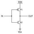
도 14은 본 발명의 실시예에 따른 반도체 소자를 포함하는 인버터의 회로도이다.
도 15는 본 발명의 실시예에 따른 반도체 소자를 포함하는 SRAM 셀의 회로도이다.
도 16 및 도 17는 본 발명의 실시예에 따른 반도체 소자를 포함하는 전자 장치 및 저장 장치를 나타낸 블록도이다.1 is a schematic perspective view of a semiconductor device according to an embodiment of the present invention.
2 is a plan view of a semiconductor device according to an embodiment of the present invention shown in FIG.
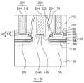
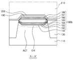
FIGS. 3A to 3D are cross-sectional views of a semiconductor device according to an embodiment of the present invention shown in FIG. 1 in a specific direction.
Figs. 4 and 5 are cross-sectional views showing various examples of the structure shown in Fig. 3A.
6 is a schematic perspective view of a semiconductor device according to an embodiment of the present invention.
7A to 7D are cross-sectional views of a semiconductor device according to an embodiment of the present invention shown in FIG. 6 in a specific direction.
8 is a schematic perspective view of a semiconductor device according to an embodiment of the present invention.
9 is a plan view of a semiconductor device according to an embodiment of the present invention shown in FIG.
FIGS. 10A to 10D are cross-sectional views of a semiconductor device according to an embodiment of the present invention shown in FIG. 8 in a specific direction.
11A to 11G are cross-sectional views of major processes for explaining a method of manufacturing a semiconductor device according to an embodiment of the present invention shown in FIG.
12 is a schematic perspective view of a semiconductor device according to an embodiment of the present invention.
FIGS. 13A to 13D are cross-sectional views of a semiconductor device according to an embodiment of the present invention shown in FIG. 12 in a specific direction.
14 is a circuit diagram of an inverter including a semiconductor device according to an embodiment of the present invention.
15 is a circuit diagram of an SRAM cell including a semiconductor device according to an embodiment of the present invention.
16 and 17 are block diagrams showing an electronic device and a storage device including a semiconductor device according to an embodiment of the present invention.
이하, 첨부된 도면을 참조하여 본 발명의 바람직한 실시 예들을 설명한다.Hereinafter, preferred embodiments of the present invention will be described with reference to the accompanying drawings.
그러나, 본 발명의 실시 형태는 여러 가지 다른 형태로 변형될 수 있으며, 본 발명의 범위가 이하 설명되는 실시 형태로 한정되는 것은 아니다. 또한, 본 발명의 실시예는 당해 기술분야에서 평균적인 지식을 가진 자에게 본 발명을 더욱 완전하게 설명하기 위해서 제공되는 것이다. 따라서, 도면에서의 요소들의 형상 및 크기 등은 보다 명확한 설명을 위해 과장될 수 있다. 또한, 본 명세서에서 '상', '상부', '상면', '하', '하부', '하면', '측면' 등의 용어는 도면을 기준으로 한 것이며, 실제로는 반도체 소자가 배치되는 방향에 따라 달라질 수 있다.However, the embodiments of the present invention can be modified into various other forms, and the scope of the present invention is not limited to the embodiments described below. Further, the embodiments of the present invention are provided to more fully explain the present invention to those skilled in the art. Accordingly, the shapes and sizes of the elements in the drawings and the like can be exaggerated for clarity. In the present specification, terms such as 'phase', 'upper', 'upper surface', 'lower', 'lower', 'lower', 'side', and the like are based on the drawings, Depending on the direction.
한편, 본 명세서에서 사용되는 "일 실시예(one example)"라는 표현은 서로 동일한 실시예를 의미하지 않으며, 각각 서로 다른 고유한 특징을 강조하여 설명하기 위해서 제공되는 것이다. 그러나, 아래 설명에서 제시된 실시예들은 다른 실시예의 특징과 결합되어 구현되는 것을 배제하지 않는다. 예를 들어, 특정한 실시예에서 설명된 사항이 다른 실시예에서 설명되어 있지 않더라도, 다른 실시예에서 그 사항과 반대되거나 모순되는 설명이 없는 한, 다른 실시예에 관련된 설명으로 이해될 수 있다.
The term " one example " used in this specification does not mean the same embodiment, but is provided to emphasize and describe different unique features. However, the embodiments presented in the following description do not exclude that they are implemented in combination with the features of other embodiments. For example, although the matters described in the specific embodiments are not described in the other embodiments, they may be understood as descriptions related to other embodiments unless otherwise described or contradicted by those in other embodiments.
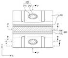
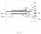
도 1은 본 발명의 일 실시예에 따른 반도체 소자의 개략적인 사시도이다. 도 2는 도 1에 도시된 본 발명의 일 실시예에 따른 반도체 소자의 평면도이다. 도 3a 내지 도 3d는 도 1에 도시된 본 발명의 일 실시예에 따른 반도체 소자의 특정 방향에 대한 단면도들이다. 구체적으로, 도 3a 내지 도 3d는 각각 도 2의 A-A' 선, B-B' 선, C-C' 선 및 D-D' 선을 따라 절단된 도 1에 도시된 반도체 소자의 단면도들이다.1 is a schematic perspective view of a semiconductor device according to an embodiment of the present invention. 2 is a plan view of a semiconductor device according to an embodiment of the present invention shown in FIG. FIGS. 3A to 3D are cross-sectional views of a semiconductor device according to an embodiment of the present invention shown in FIG. 1 in a specific direction. 3A to 3D are cross-sectional views of the semiconductor device shown in FIG. 1 taken along line A-A ', line B-B', line C-C ', and line D-D', respectively, in FIG.
도 1 및 도 3a 내지 도 3d를 참조하면, 본 발명의 일 실시예에 따른 반도체 소자(100A)는 소자 분리막(130)에 의해 활성 영역(ACT)이 정의된 반도체 기판(110), 활성 영역(ACT)을 가로지르며 배치된 게이트 전극(220), 게이트 전극(220) 아래에 배치된 게이트 절연막(140), 게이트 전극(220)의 양 측벽에 배치된 스페이서(170), 게이트 전극(220)의 양 측의 활성 영역(ACT) 내에 배치되며, 불순물로 도핑된 소스 영역(SR) 및 드레인 영역(DR), 활성 영역(ACT) 내에서 소스 영역(SR) 및 드레인 영역(DR) 사이에 배치되며 게이트 절연막(140) 아래에 배치된 채널 영역(CHR)을 포함할 수 있다. 또한, 소스 영역(SR) 및 드레인 영역(DR)의 적어도 일부분에 배치되며 게이트 절연막(140)보다 융기된 상면을 가지는 실리콘 게르마늄(SiGe) 에피택셜층(180), 실리콘 게르마늄 에피택셜층(180) 상에 배치된 실리콘 캡핑층(190), 게이트 전극(220)의 측벽, 소자 분리막(130), 및 실리콘 캡핑층(190) 상에 배치된 식각 정지층(200) 및 층간 절연막(210), 그리고 실리콘 게르마늄 에피택셜층(180)에 연결된 콘택 플러그(240)를 포함할 수 있다.A
본 발명의 일 실시예에서 반도체 기판(110)은 n형으로 도핑된 단결정 실리콘 기판일 수 있다. 또는 반도체 기판(110)은 단결정 실리콘 웨이퍼에서 n형으로 도핑된 일 영역일 수 있다. 소자 분리막(130)은 BPSG(Boron-Phosphor Slilicate Glass)막, HDP(High Density Plasma)막, FOX(Flowable OXide)막, TOSZ(TOnen SilaZene)막, SOG(Spin On Glass)막, USG(Undoped Silica Glass) 막, TEOS(TetraEthyl Ortho Silicate) 막, LTO(Low Temperature Oxide)막 중 적어도 어느 하나로 이루어질 수 있다.In one embodiment of the present invention, the
게이트 절연막(140)은 실리콘 산화막, 실리콘 산질화막, 실리콘 질화막 및 고유전막들 중에서 적어도 하나를 포함할 수 있으며, 복수의 막들로 구성될 수 있다. 상기 고유전막은 실리콘 산화막보다 높은 유전 상수를 갖는 절연성 물질들을 의미하며, 탄탈륨 산화막, 티타늄 산화막, 하프늄 산화막, 지르코늄 산화막, 알루미늄 산화막, 이트륨 산화막, 니오븀 산화막, 하프늄 실리케이트, 지르코늄 실리케이트 중 적어도 하나일 수 있다.The
게이트 전극(220)은 제1 게이트 전극(222) 및 제2 게이트 전극(224)을 포함할 수 있고, 제1 게이트 전극(222)는 금속 질화물로 이루어질 수 있다. 예를 들어, 제1 게이트 전극(222)은 티타늄 질화막(TiN), 탄탈륨 질화막(TaN), 또는 텅스텐 질화막(WN) 등 중의 적어도 하나로 이루어질 수 있다. 제2 게이트 전극(224)는 금속 물질로 이루어질 수 있다. 제2 게이트 전극(224)은 예를 들어, 알루미늄(Al), 텅스텐(W), 또는 몰리브데넘(Mo) 등 중의 적어도 하나로 이루어질 수 있다. 제1 게이트 전극(222)는 제2 게이트 전극(224)을 이루는 금속 물질에 대한 확산 방지막으로서 역할을 할 수 있다.The
식각 정지층(200)은 실리콘 질화막 또는 실리콘 산질화막일 수 있고, 층간 절연막(210)은 실리콘 산화막, TEOS(TetraEthylOrthoSilicate), USG(Undoped Silicate Glass), PSG(PhosphoSilicate Galss), BSG(BoroSilicate Glass), BPSG(BoroPhosphoSilicate Glass), FSG(Fluoride Silicate Glass), SOG(Spin On Glass), TOSZ(Tonen SilaZene) 또는 이들의 조합으로 이루어질 수 있다.
The
도 3a를 참조하여, 실리콘 게르마늄 에피택셜층(180)에 대해 더욱 구체적으로 설명한다. 도면을 참조하여 드레인 영역(DR)을 기준으로 설명하지만, 소스 영역(SR)도 동일한 구조를 가질 수 있다.Referring to FIG. 3A, the silicon
점선으로 표시된 드레인 영역(DR)은 활성 영역(ACT) 내에 고농도로 도핑된 불순물 영역일 수 있고, 드레인 영역(DR) 내 의 리세스 영역(150) 상에 배치된 실리콘 게르마늄 에피택셜층(180)은 게르마늄의 농도가 서로 다른 4개의 층을 포함할 수 있다.The drain region DR indicated by the dashed line may be a heavily doped impurity region in the active region ACT and the silicon
드레인 영역(DR)의 적어도 일부분을 제거하여 형성된 리세스 영역(150) 내에 버퍼 에피택셜층(182)가 최하부에 배치되고, 버퍼 에피택셜층(182) 상에 차례로 제1 에피택셜층(184), 제2 에피택셜층(186), 및 제3 에피택셜층(188)이 배치될 수 있다. 리세스 영역(150)의 바닥면은 반도체 기판(110)의 표면에 평행할 수 있고, 소자 분리막(130)에 인접한 리세스 영역(150)의 측면은 바닥면에 대해 경사를 가질 수 있다. 실리콘 게르마늄 에피택셜층(180)의 상면은 반도체 기판(110)의 표면에 평행할 수 있고, 소자 분리막(130)에 인접한 실리콘 게르마늄 에피택셜층(180)의 측면은 상면에 대해 경사를 가질 수 있다. 실리콘 게르마늄 에피택셜층(180)의 상면은 활성 영역(ACT)의 상면보다 높이 위치할 수 있다. 이와 같은 융기된(elevated) 소스 및 드레인 구조는 소스 및 드레인 영역의 단면적을 증가시키는 효과가 있으므로, 소스 영역 및 드레인 영역의 저항을 개선할 수 있다.A
게르마늄(Ge)의 농도는 버퍼 에피택셜층(182)이 가장 낮을 수 있고, 제2 에피택셜층(186)이 가장 높을 수 있다. 구체적으로, 버퍼 에피택셜층(182)의 게르마늄의 농도는 10 내지 25 at%(atomic percent), 제1 에피택셜층(184)의 게르마늄의 농도는 25 내지 50 at%, 제2 에피택셜층(186)의 게르마늄의 농도는 50 내지 90 at%, 그리고 제3 에피택셜층(188)의 게르마늄의 농도는 25 내지 50 at%일 수 있다. 버퍼 에피택셜층(182)은 제1 에피택셜층(184)과 실리콘으로 이루어진 활성 영역(ACT)간의 격자 불일치(lattice mismatch)를 감소시켜 실리콘 게르마늄 에피택셜층(180) 내의 격자 결함을 감소시키는 역할을 할 수 있다. 각 에피택셜층(182, 184, 186, 188)의 두께는 서로 다를 수 있으며, 예를 들어, 게르마늄의 농도가 가장 높아서 채널 영역에 압축성 스트레인을 가장 많이 유발할 수 있는 제2 에피택셜층(186)의 두께가 가장 두꺼울 수 있다.The concentration of germanium (Ge) may be the lowest in the
실리콘 게르마늄 에피택셜층(180)은 고농도의 p형 불순물로 도핑되어 소스 영역 및 드레인 영역의 적어도 일부를 이룰 수 있다. 고농도의 p형 불순물의 도핑은 실리콘 게르마늄 에피택셜층(180)을 성장하는 동안에 인시츄(in-situ) 도핑을 통해 이루어질 수 있다. 이와 달리, 고농도의 p형 불순물의 도핑은 실리콘 게르마늄 에피택셜층(180)의 성장이 완료된 후 실리콘 게르마늄 에피택셜층(180) 상에 형성된 실리콘 캡핑층(190)을 버퍼층으로 이용하여 이온 주입 공정에 의해 이루어질 수도 있다. 실리콘 게르마늄 에피택셜층(180) 내의 p형 불순물의 농도는 게르마늄의 농도에 비례하여 변할 수 있으며, 예를 들어, 제2 에피택셜층(186) 내에서 가장 높은 농도로 형성될 수 있다. 일 실시예에서 p형 불순물은 보론(B)일 수 있다.
The silicon
도 3b 및 도 3d를 참조하여, 실리콘 게르마늄 에피택셜층(180)에 연결된 콘택 플러그(240)에 대해 더욱 구체적으로 설명하면, 콘택 플러그(240)은 제1 콘택 플러그(242) 및 제2 콘택 플러그(244)를 포함할 수 있다. 제1 콘택 플러그(242)는 금속 질화물로 이루어질 수 있다. 예를 들어, 티타늄 질화막(TiN), 탄탈륨 질화막(TaN), 또는 텅스텐 질화막(WN) 등 중의 적어도 하나로 이루어질 수 있다. 제2 콘택 플러그(244)는 금속 물질로 이루어질 수 있다. 예를 들어, 알루미늄(Al), 텅스텐(W), 또는 몰리브데넘(Mo) 등 중의 적어도 하나로 이루어질 수 있다. 제1 콘택 플러그(242)는 제2 콘택 플러그(244)를 이루는 금속 물질에 대한 확산 방지막으로서 역할을 할 수 있다.3B and 3D, a
실리콘 게르마늄 에피택셜층(180)과 콘택 플러그(240) 사이에 금속 실리사이드(230)이 더 배치될 수 있다. 금속 실리사이드(230)은 니켈 실리사이드, 코발트 실리사이드, 텅스텐 실리사이드, 티타늄 실리사이드, 탄탈륨 실리사이드, 또는 니오븀 실리사이드 등 중에서 하나일 수 있다.A
반도체 소자(100A)는 PMOS 트랜지스터일 수 있으며, PMOS 트랜지스터의경우, 채널 영역에서 다수 캐리어(major carrier)인 정공의 이동도(mobility)가 증가하면 PMOS 트랜지스터의 성능(performance)이 향상될 수 있다. 또한, 소스 영역 및 드레인 영역에서의 저항이나 콘택 저항이 감소되면 PMOS 트랜지스터의 성능이 향상될 수 있다. 채널 영역에서 정공의 이동도를 증가시키는 방법 중의 하나로 소스 영역 및 드레인 영역의 일부에 임베디드 실리콘 게르마늄(eSiGe) 에피택셜층을 배치시키는 것이 이용될 수 있다. 게르마늄의 격자 상수가 실리콘의 격자 상수보다 크므로, 실리콘 게르마늄의 격자 상수는 실리콘의 격자 상수보다 크고 게르마늄의 격자 상수보다 작을 수 있다. 따라서, 임베디드 실리콘 게르마늄(eSiGe) 에피택셜층은 PMOS 트랜지스터의 채널 영역에 일축 압축성 스트레인(uniaxial compressive strain)을 유발할 수 있다. 게르마늄의 농도가 증가할수록 채널 영역에 유발되는 일축 압축성 스트레인은 더 커질 수 있다. 이러한 일축 압축성 스트레인은 채널 영역에서 정공의 이동도를 증가시킬 수 있다.The
본 발명의 일 실시예에서, 콘택 플러그(240)가 층간 절연막(210)을 관통하여 제3 에피택셜층(188)까지 연장되고, 콘택 플러그(240)와 제2 에피택셜층(186)의 사이에 금속 실리사이드(230)가 배치될 수 있다. 실시예에 따라, 콘택 플러그(440)은 실리콘 캡핑층(390)까지 연장되도록 형성되고, 금속 실리사이드(430)는 제3 에피택셜층(388) 내에 형성되어 제2 에피택셜층(386)에 접할 수 있다. 즉 실리콘 캡핑층(390)의 상면으로부터 제3 에피택셜층(388)의 하부까지의 두께(d3)보다 실리콘 캡핑층(390)의 상면으로부터 금속 실리사이드층(430)의 하부까지의 두께(d4)가 같을 수 있다. 이와 같이 제2 에피택셜층(186) 상에 제3 에피택셜층(188)을 배치시킴으로써 콘택 식각 공정 및 금속 실리사이드 공정에 의해 게르마늄의 농도가 가장 높은 제2 에피택셜층(186)이 손실되는 것을 방지할 수 있으므로, 채널 영역(CHR)에 일축 압축성 스트레인(uniaxial compressive strain)을 효율적으로 유발할 수 있다. 뿐만 아니라, 게르마늄(Ge) 및 p형 불순물(예를 들어, 보론(B))의 농도가 가장 높은 제2 에피택셜층(186)에서 쇼트키 콘택이 형성되므로, 쇼트키 배리어 높이 및 폭이 낮아져 콘택 저항을 낮출 수 있다. 결국, PMOS 트랜지스터의 성능을 향상시킬 수 있다.
The
도 4 및 도 5는 본 발명의 일 실시예에 따른 반도체 소자를 개략적으로 도시하는 단면도들이다. 구체적으로, 도 4 및 도 5는 도 3a에 대응되는 단면을 도시한다.4 and 5 are cross-sectional views schematically showing a semiconductor device according to an embodiment of the present invention. Specifically, Figs. 4 and 5 show cross sections corresponding to Fig. 3A.
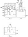
도 4를 참조하면, 실리콘 게르마늄 에피택셜층(180a)은 게르마늄의 농도가 서로 다른 3개의 층을 포함할 수 있다. 리세스 영역(150)의 최하부에 제1 에피택셜층(184a)이 배치되고, 그 위에 게르마늄 농도가 가장 높은 제2 에피택셜층(186a) 및 제3 에피택셜층(188a)이 배치될 수 있다. 제2 에피택셜층(186a) 및 제3 에피택셜층(188a)의 게르마늄의 농도는 도 3a를 참조하여 설명한 것과 동일할 수 있다. 한편, 제1 에피택셜층(184a)의 게르마늄 농도는 하부에서 상부로 갈수록 농도가 증가하는 농도 경사(concentration gradient)를 가지며 10 내지 50 at%(atomic percent) 범위 내에서 변할 수 있다.Referring to FIG. 4, the silicon
도 5를 참조하면, 실리콘 게르마늄 에피택셜층(180b)은 게르마늄의 농도가 서로 다른 4개의 층을 포함하고, 이들 층 사이에 3개의 계면층을 더 포함할 수 있다. 도 3a를 참조하여 설명한 버퍼 에피택셜층(182) 및 제1 에피택셜층(184) 사이에 제1 계면층(183)을, 제1 에피택셜층(184) 및 제2 에피택셜층(186) 사이에 제2 계면층(185)을, 그리고 제2 에피택셜층(186) 및 제3 에피택셜층(188) 사이에 제3 계면층(187)을 더 포함할 수 있다. 각 계면층의 게르마늄의 농도는 상부 및 하부 에피택셜층의 게르마늄의 농도의 사이에서 농도 경사를 가지며 변할 수 있다.
Referring to FIG. 5, the silicon
도 6은 본 발명의 일 실시예에 따른 반도체 소자의 개략적인 사시도이다. 도 7a 내지 도 7d는 본 발명의 일 실시예에 따른 반도체 소자의 특정 방향에 대한 단면도들이다. 구체적으로, 도 7a 내지 도 7d는 각각 도 2의 A-A' 선, B-B' 선, C-C' 선, 및 D-D' 선을 따라 자른 도 6에 도시된 반도체 소자의 단면도들이다.6 is a schematic perspective view of a semiconductor device according to an embodiment of the present invention. 7A to 7D are cross-sectional views of a semiconductor device according to an exemplary embodiment of the present invention. 7A to 7D are cross-sectional views of the semiconductor device shown in FIG. 6 taken along line A-A ', line B-B', line C-C ', and line D-D', respectively, in FIG.
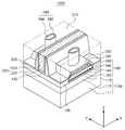
도 6에 도시된 본 발명의 일 실시예에 따른 반도체 소자(100B)는 도 1에 도시된 반도체 소자(100A)와 달리, 반도체 기판(110a)이 에스오아이(Silicon on Insulator; SOI) 기판인 경우이다. 따라서, 도 1 및 도 3a 내지 도 3d에 대한 설명과 중복되는 설명은 생략한다.The
에스오아이(SOI) 기판은 SIMOX(Separation by Implated Oxygen)와 BESOI(Bonded and Etch back SOI) 등의 제조 방법으로 제작된 것일 수 있다. SOI 기판은 실리콘 기판(111), 실리콘 기판 상의 절연층(115) 및 절연층 상의 실리콘층(silicon on insulator)(119)를 포함할 수 있다. 도시되지는 않았으나, 절연층(115)와 실리콘층(119) 사이에 실리콘 게르마늄층이 더 포함될 수 있다.
The SOI substrate may be manufactured by a manufacturing method such as SIMOX (Separation by Implanted Oxygen) and BESOI (Bonded and Etch back SOI). The SOI substrate may include a
도 7a 내지 도 7d를 참조하면, 본 실시예에서는 활성 영역(ACT)을 이루는 실리콘층이 도 1 및 도 3a 내지 도 3d를 참조하여 설명한 반도체 소자에 비해 얇으므로, 실리콘 게르마늄 에피택셜층(180)에 포함된 각 에피택셜층들(182, 184, 186, 188)의 두께들이 얇아질 수 있다. 본 실시예에서도 도 4 및 도 5를 참조하여 설명한 실리콘 게르마늄 에피택셜층들(180a, 180b)이 적용될 수 있다.Referring to FIGS. 7A to 7D, the silicon
본 실시예에서 게이트 전극(220) 아래의 실리콘은 부분적으로 공핍(partially depleted)되거나 완전 공핍(fully depleted)될 수 있다.
In this embodiment, the silicon under the
도 8은 본 발명의 일 실시예에 따른 반도체 소자의 개략적인 사시도이다.8 is a schematic perspective view of a semiconductor device according to an embodiment of the present invention.
도 8은 본 발명의 일 실시예에 따른 반도체 소자의 개략적인 사시도이다. 도 9는 도 8에 도시된 본 발명의 일 실시예에 따른 반도체 소자의 평면도이다. 도 10a 내지 도 10d는 도 8에 도시된 본 발명의 일 실시예에 따른 반도체 소자의 특정 방향에 대한 단면도들이다. 구체적으로, 도 10a 내지 도 10d는 각각 도 9의 A-A' 선, B-B' 선, C-C' 선 및 D-D' 선을 따라 자른 도 8에 도시된 반도체 소자의 단면도들이다.8 is a schematic perspective view of a semiconductor device according to an embodiment of the present invention. 9 is a plan view of a semiconductor device according to an embodiment of the present invention shown in FIG. FIGS. 10A to 10D are cross-sectional views of a semiconductor device according to an embodiment of the present invention shown in FIG. 8 in a specific direction. Specifically, FIGS. 10A to 10D are cross-sectional views of the semiconductor device shown in FIG. 8, taken along line A-A ', line B-B', line C-C ', and line D-D', respectively, in FIG.
도 8 및 도 10a 내지 도 10d를 참조하면, 본 발명의 일 실시예에 따른 반도체 소자(300A)는 소자 분리막(330)에 의해 활성 영역(ACT)이 정의된 반도체 기판(310), 활성 영역(ACT)을 가로지르며 배치된 게이트 전극(420), 게이트 전극(420) 아래에 배치된 게이트 절연막(340), 게이트 전극(420)의 양 측벽에 배치된 스페이서(370), 게이트 전극(420)의 양 측의 활성 영역(ACT) 내에 배치되며, 불순물로 도핑된 소스 영역(SR) 및 드레인 영역(DR), 활성 영역(ACT) 내에서 소스 영역(SR) 및 드레인 영역(DR) 사이에 배치되며 게이트 절연막(340) 아래에 배치된 채널 영역(CHR)을 포함할 수 있다. 또한, 소스 영역(SR) 및 드레인 영역(DR)의 적어도 일부분에 배치되며 게이트 절연막(340)보다 융기된 상면을 가지는 실리콘 게르마늄 에피택셜층(380), 실리콘 게르마늄 에피택셜층(380) 상에 배치된 실리콘 캡핑층(390), 게이트 전극(420)의 측벽, 소자 분리막(330), 및 실리콘 게르마늄 에피택셜층(380) 상에 배치된 식각 정지층(400) 및 층간 절연막(410), 그리고 실리콘 게르마늄 에피택셜층(380)에 연결된 콘택 플러그(440)를 포함할 수 있다.8A and 10A to 10D, a
본 발명의 일 실시예에서 반도체 기판(310)은 n형으로 도핑된 단결정 실리콘 기판일 수 있다. 소자 분리막(330)은 BPSG(Boron-Phosphor Slilicate Glass)막, HDP(High Density Plasma)막, FOX(Flowable OXide)막, TOSZ(TOnen SilaZene)막, SOG(Spin On Glass)막, USG(Undoped Silica Glass) 막, TEOS(TetraEthyl Ortho Silicate) 막, LTO(Low Temperature Oxide)막 중 적어도 어느 하나로 이루어질 수 있다. 활성 영역(ACT) 각각은 상부로 연장되면서 폭이 좁아지는 형상을 가질 수 있다. 또한, 활성 영역들(ACT)은 일 방향, 예를 들어 y 방향으로 연장될 수 있다. 도면 상에는 2개의 활성 영역들(ACT)이 도시되어 있지만, 활성 영역들(ACT)의 개수는 이에 한정되지 않는다. 소자 분리막(330)은 활성 영역들(ACT) 사이에 소정의 높이로 채워져 있으며, 소자 분리막(330) 위로 돌출된 활성 영역(ACT)의 상부 영역을 활성 핀(AF)이라 지칭한다.In one embodiment of the present invention, the
게이트 절연막(340)은 실리콘 산화막, 실리콘 산질화막, 실리콘 질화막 및 고유전막들 중에서 적어도 하나를 포함할 수 있으며, 복수의 막들로 구성될 수 있다. 상기 고유전막은 실리콘 산화막보다 높은 유전 상수를 갖는 절연성 물질들을 의미하며, 탄탈륨 산화막, 티타늄 산화막, 하프늄 산화막, 지르코늄 산화막, 알루미늄 산화막, 이트륨 산화막, 니오븀 산화막, 하프늄 실리케이트, 지르코늄 실리케이트 중 적어도 하나일 수 있다.The
게이트 전극(420)은 제1 게이트 전극(422) 및 제2 게이트 전극(424)을 포함할 수 있고, 제1 게이트 전극(422)는 금속 질화물로 이루어질 수 있다. 예를 들어, 티타늄 질화막(TiN), 탄탈륨 질화막(TaN), 또는 텅스텐 질화막(WN) 등 중의 적어도 하나로 이루어질 수 있다. 제2 게이트 전극(424)는 금속 물질로 이루어질 수 있다. 예를 들어, 알루미늄(Al), 텅스텐(W), 또는 몰리브데넘(Mo) 등 중의 적어도 하나로 이루어질 수 있다. 제1 게이트 전극(422)는 제2 게이트 전극(424)을 이루는 금속 물질에 대한 확산 방지막으로서 역할을 할 수 있다.The
식각 정지층(400)은 실리콘 질화막 또는 실리콘 산질화막일 수 있고, 층간 절연막(410)은 실리콘 산화막, TEOS(TetraEthylOrthoSilicate), USG(Undoped Silicate Glass), PSG(PhosphoSilicate Galss), BSG(BoroSilicate Glass), BPSG(BoroPhosphoSilicate Glass), FSG(Fluoride Silicate Glass), SOG(Spin On Glass), TOSZ(Tonen SilaZene) 또는 이들의 조합으로 이루어질 수 있다.
The
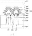
도 10a를 참조하여, 실리콘 게르마늄 에피택셜층(380)에 대해 더욱 구체적으로 설명하면, 활성 영역(ACT) 내의 드레인 영역(DR)의 적어도 일부분에 배치된 실리콘 게르마늄 에피택셜층(380)은 게르마늄의 농도가 서로 다른 4개의 층을 포함할 수 있다. 도면에 따라 드레인 영역(DR)을 기준으로 설명하지만, 소스 영역(SR)에 대해서도 마찬가지로 적용될 수 있다.10A, the silicon
드레인 영역(DR)의 적어도 일부분을 제거하여 형성된 리세스 영역(350) 내에 버퍼 에피택셜층(382)가 최하부에 배치되고, 버퍼 에피택셜층(382) 상에 차례로 제1 에피택셜층(384), 제2 에피택셜층(386), 및 제3 에피택셜층(388)이 배치될 수 있다. 리세스 영역(350)은 반도체 기판(310)의 표면에 평행한 바닥면과 경사진 측면들을 포함할 수 있다. 도 10a에서는 리세스 영역(350)의 바닥면이 소자 분리막(330)의 상면과 동일한 높이로 도시되어 있으나, 실리콘 게르마늄 에피택셜층(380)은 반도체 기판(310)의 표면에 평행한 상면 및 경사진 측면들을 포함할 수 있고, 실리콘 게르마늄 에피택셜층(380)의 상면은 활성 영역(ACT)의 상면보다 높이 위치할 수 있다. 이와 같은 융기된(elevated) 소스 및 드레인 구조는 소스 영역 및 드레인 영역의 저항을 개선할 수 있다. 실리콘 게르마늄 에피택셜층(380)은 특정한 경사면들을 가질 수 있고, 이웃하는 활성 핀(AF)들로부터 성장된 실리콘 게르마늄 에피택셜층(380)들은 적어도 일부분이 서로 머지(merge)된 구조를 가질 수 있다. 구체적으로, 제3 에피택셜층(388)의 일부분이 서로 연결된 구조일 수 있다. 다만, 이에 제한되지 않는다. 머지(merge)된 실리콘 게르마늄 에피택셜층(380)과 소자 분리막(330) 사이의 삼각 영역(405)는 에어갭(air gap)일 수 있다.A
게르마늄의 농도는 버퍼 에피택셜층(382)이 가장 낮을 수 있고, 제2 에피택셜층(386)이 가장 높을 수 있다. 구체적으로, 버퍼 에피택셜층(382)의 게르마늄의 농도는 10 내지 25 at%, 제1 에피택셜층(384)의 게르마늄의 농도는 25 내지 50 at%, 제2 에피텍층(186)의 게르마늄의 농도는 50 내지 90 at%, 그리고 제3 에피택셜층(188)의 게르마늄의 농도는 25 내지 50 at%일 수 있다. 버퍼 에피택셜층(382)은 하부 에피택셜층(384)와 실리콘으로 이루어진 활성 영역(ACT)간의 격자 불일치(lattice mismatch)를 줄여서 실리콘 게르마늄 에피택셜층(180) 내의 격자 결함을 줄여주는 역할을 할 수 있다. 각 에피택셜층(382, 384, 386, 388)의 두께는 서로 다를 수 있고, 제2 에피택셜층(386)의 두께가 가장 두꺼울 수 있다. 각 에피택셜층(382, 384, 386, 388)의 두께 비율은 도시된 바에 의해 제한되지 않으며, 필요에 따라 적절히 조절될 수 있다. 본 실시예에서도 도 4 및 도 5를 참조하여 설명한 실리콘 게르마늄 에피택셜층들(180a, 180b)이 적용될 수 있다.
The concentration of germanium may be lowest for the
실리콘 게르마늄 에피택셜층(380)은 고농도의 p형 불순물로 도핑되어 소스 영역 및 드레인 영역의 적어도 일부를 이룰 수 있다. 고농도의 p형 불순물의 도핑은 실리콘 게르마늄 에피택셜층(380)을 성장하는 동안에 인시츄(in-situ) 도핑을 통해 이루어질 수 있다. 이와 달리, 실리콘 게르마늄 에피택셜층(380)의 성장이 완료된 후 그 상에 형성된 실리콘 캡핑층(390)을 버퍼층으로 사용한 이온 주입 공정에 의해 이루어질 수도 있다. 실리콘 게르마늄 에피택셜층(380) 내의 p형 불순물의 농도는 게르마늄의 농도에 비례하여 변할 수 있고, 제2 에피택셜층(386) 내에서 가장 높은 농도로 형성될 수 있다. 본 실시예에서 p형 불순물은 보론(B)일 수 있다.
The silicon
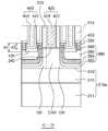
도 10b 및 도 10d를 참조하여, 실리콘 게르마늄 에피택셜층(380)에 연결된 콘택 플러그(440)에 대해 더욱 구체적으로 설명하면, 콘택 플러그(440)은 이웃하는 2개의 활성 핀들(AF) 상에서 머지(merge)된 구조를 가지는 실리콘 게르마늄 에피택셜층들(380)에 연결되도록 게이트 전극(420)에 나란한 방향으로 연장되는 장방형의 형태를 가질 수 있다. 이러한 구조는 콘택의 접촉 면적을 늘려 콘택 저항을 감소시키는 데 유리할 수 있다. 콘택 플러그(440)의 하단부의 형상이 실리콘 게르마늄 에피택셜(380)의 상단부의 형상에 대응되게 굴곡진 형상을 가질수 있다. 다만, 이에 제한되지 않고, 식각 조건에 따라 굴곡진 형상이 더욱 완만해지거나 평평한 형상으로 될 수 있다.Referring more particularly to the
콘택 플러그(440)은 제1 콘택 플러그(442) 및 제2 콘택 플러그(444)를 포함할 수 있다. 제1 콘택 플러그(442)는 금속 질화물로 이루어질 수 있다. 예를 들어, 티타늄 질화막(TiN), 탄탈륨 질화막(TaN), 또는 텅스텐 질화막(WN) 등 중의 적어도 하나로 이루어질 수 있다. 제2 콘택 플러그(444)는 금속 물질로 이루어질 수 있다. 예를 들어, 알루미늄(Al), 텅스텐(W), 또는 몰리브데넘(Mo) 등 중의 적어도 하나로 이루어질 수 있다. 제1 콘택 플러그(442)는 제2 콘택 플러그(444)를 이루는 금속 물질에 대한 확산 방지막으로서 역할을 할 수 있다.The
실리콘 게르마늄 에피택셜층(380)과 콘택 플러그(340) 사이에 금속 실리사이드(330)이 더 배치될 수 있다. 금속 실리사이드(330)은 니켈 실리사이드, 코발트 실리사이드, 텅스텐 실리사이드, 티타늄 실리사이드, 탄탈륨 실리사이드, 또는 니오븀 실리사이드 등 중에서 하나일 수 있다.A
본 발명의 일 실시예에서, 콘택 플러그(440)가 층간 절연막(410)을 관통하여 제3 에피택셜층(388)까지 연장되도록 형성되고, 금속 실리사이드(430)가 제2 에피택셜층(386)의 상부 영역에 형성될 수 있다. 실시예에 따라, 콘택 플러그(440)은 실리콘 캡핑층(390)까지 연장되도록 형성되고, 금속 실리사이드(430)는 제3 에피택셜층(388) 내에 형성되어 제2 에피택셜층(386)에 접할 수 있다. 즉 실리콘 캡핑층(390)의 상면으로부터 제3 에피택셜층(388)의 하부까지의 두께(d3)보다 실리콘 캡핑층(390)의 상면으로부터 금속 실리사이드층(430)의 하부까지의 두께(d4)가 같을 수 있다.The
이와 같이 제2 에피택셜층(386) 상에 제3 에피택셜층(388)을 배치시킴으로써 콘택 식각 및 금속 실리사이드 공정에 의해 게르마늄의 농도가 가장 높은 제2 에피택셜층(386)이 손실되는 것을 방지할 수 있고, 이로 인해 채널 영역(CHR)에 일축 압축성 스트레인(uniaxial compressive strain)을 효율적으로 유발할 수 있다. 뿐만 아니라, 게르마늄(Ge) 및 p형 불순물(예를 들어, 보론(B))의 농도가 가장 높은 제2 에피택셜층(386)에서 쇼트키 콘택이 형성되므로, 쇼트키 배리어 높이 및 폭이 낮아져 콘택 저항을 낮출 수 있다. 결국, PMOS 트랜지스터의 성능을 향상시킬 수 있다.By thus disposing the
실제로 비교 평가한 결과에서도, 본 발명의 일 실시예에 따른 PMOS 트랜지스터는 게르마늄(Ge) 조성이 낮은 층을 버퍼층으로 사용하고 순차적으로 게르마늄(Ge) 조성을 늘려 게르마늄(Ge) 조성이 가장 높은 층을 최상부에 위치하도록 형성된 실리콘 게르마늄 에피택셜층을 포함하는 PMOS 트랜지스터에 비해, 테스트 조건에서 콘택 저항이 약 25 % 감소하고, 전류값이 약 5 % 증가되었다.
As a result of the actual comparison, the PMOS transistor according to an embodiment of the present invention uses a layer having a low germanium (Ge) composition as a buffer layer and sequentially increases the composition of germanium (Ge) The contact resistance was reduced by about 25% and the current value was increased by about 5% in the test condition, as compared with the PMOS transistor including the silicon germanium epitaxial layer formed to be located in the contact hole.
도 11a 내지 도 11g는 본 발명의 일 실시예에 따른 반도체 소자의 제조방법을 설명하기 위한 주요 공정별 단면도들이다.11A to 11G are cross-sectional views of major processes for explaining a method of manufacturing a semiconductor device according to an embodiment of the present invention.
이들 각각은 도 9의 절단선들 B-B' 선, C-C' 선 및 D-D' 선을 따라 자른 주요 공정별 단면도들이다. 이들 도면 중 일부에서는 절단선 C-C' 선에 따른 단면도와 동일하여 절단선 B-B' 선에 따른 단면도는 생략된다.Each of which is a cross-sectional view along the line B-B ', line C-C', and line D-D 'of FIG. In some of these drawings, the same as the sectional view taken along the line C-C 'in the drawing, and the sectional view taken along the line B-B' is omitted.
도 11a 내지 도 11g를 참조하여, 반도체 기판(310)이 벌크 실리콘 기판인 경우에 대해 예시적으로 설명한다. 하지만, 이에 한정되지 않으며, 에스오아이(SOI) 기판인 경우에도 모순되지 않는 한 동일한 공정이 적용될 수 있다.Referring to FIGS. 11A to 11G, a case where the
도 11a를 참조하면, 반도체 기판(310)을 패터닝하여 활성 영역들(ACT)을 정의하는 소자 분리 트렌치(305)를 형성할 수 있다. 반도체 기판(310)은 불순물이 도핑된 웰(well) 영역을 포함할 수 있고, 본 발명의 일 실시예에서는 n형 불순물이 도핑된 웰 영역을 포함할 수 있다.Referring to FIG. 11A, a
소자 분리 트렌치(305)를 형성하는 단계는 반도체 기판(310) 상에 마스크 패턴들을 형성한 후, 이를 식각 마스크로 사용하여 반도체 기판(310)을 이방적으로 식각하는 단계를 포함할 수 있다. 상기 마스크 패턴은, 서로 식각 선택성을 가지며 차례로 적층되는 제1 마스크 패턴(315)와 제2 마스크 패턴(320)을 포함할 수 있다. 소자분리 트렌치들(305) 각각은 아래로 갈수록 폭이 좁아지도록 형성될 수 있고 이에 따라 활성 영역들(ACT) 각각은 위로 갈수록 폭이 좁아지도록 형성될 수 있다. 또한, 활성 영역들(ACT)은 일 방향으로 연장되어 형성될 수 있다.The step of forming the
도 11b를 참조하면, 소자 분리 트렌치(305)를 소정의 높이로 채우는 소자 분리막(330)을 형성할 수 있다. 소자 분리막(330)을 형성하는 단계는 소자 분리 트렌치(305)를 채우는 절연막을 형성한 후 이를 CMP(Chemical Mechanical Polishing) 공정을 이용해 평탄화하여 제2 마스크 패턴(320)의 상면을 노출시키는 단계를 포함할 수 있다. 소자 분리 트렌치(305)를 채우는 절연막은 BPSG(Boron-Phosphor Slilicate Glass)막, HDP(High Density Plasma)막, FOX(Flowable OXide)막, TOSZ(TOnen SilaZene)막, SOG(Spin On Glass)막, USG(Undoped Silica Glass) 막, TEOS(TetraEthyl Ortho Silicate) 막, LTO(Low Temperature Oxide)막 중 적어도 어느 하나일 수 있다.Referring to FIG. 11B, the
다음으로, 활성 영역들(ACT)의 상부영역들을 노출시킬 수 있다. 활성 영역들(ACT)의 상부 영역들을 노출시키는 단계는 건식 또는 습식 식각 기술을 사용하여 절연막을 리세스(recess) 시키는 단계를 포함할 수 있다. 이 단계에서 제1 및 제2 마스크 패턴(315, 320)이 제거될 수 있고, 이에 따라 활성 영역들(ACT)의 상면이 노출될 수 있다. 활성 영역들(ACT)의 상면은 모서리가 식각되어 곡면으로 형성될 수 있다. 소자 분리막(330) 상으로 돌출된 활성 영역들(ACT)의 상부 영역을 활성 핀들(AF)로 지칭한다.Next, the upper regions of the active regions ACT may be exposed. The step of exposing the upper regions of the active regions ACT may include recessing the insulating layer using dry or wet etching techniques. In this step, the first and
도 11c를 참조하면, 활성 핀들(AF)을 덮는 게이트 절연막(340) 및 게이트 절연막(340) 상의 희생 게이트(360)을 형성할 수 있다. 게이트 절연막(340)은 실리콘 산화막, 실리콘 산질화막, 실리콘 질화막 및 고유전막들 중에서 적어도 하나를 포함할 수 있으며, 복수의 막들로 구성될 수 있다. 고유전막은 실리콘 산화막보다 높은 유전 상수를 갖는 절연성 물질들을 의미하며, 탄탈륨 산화막, 티타늄 산화막, 하프늄 산화막, 지르코늄 산화막, 알루미늄 산화막, 이트륨 산화막, 니오븀 산화막, 하프늄 실리케이트, 지르코늄 실리케이트 중 적어도 하나일 수 있다. 희생 게이트(360)은 게이트 절연막(340)에 대해 식각 선택성을 갖는 적어도 하나의 막을 포함할 수 있다. 본 발명의 일 실시예에서 희생 게이트(360)은 게이트 절연막(340) 상에 차례로 적층되는 제1 희생 게이트(362) 및 제2 희생 게이트(364)을 포함할 수 있다. 희생 게이트(360)을 형성하는 단계는 게이트 절연막(340) 상에 제1 희생막 및 제2 희생막을 차례로 적층하여 희생 게이트막을 형성한 후, 게이트 절연막(340)을 식각 정지층으로 사용하여 상기 희생 게이트막을 이방적으로 식각하는 단계를 포함할 수 있다.Referring to FIG. 11C, a
다음으로, 희생 게이트(360)의 양측의 반도체 기판(310) 내에, 구체적으로 활성 영역들(ACT) 내에 불순물 영역인 소스 영역(SR) 및 드레인 영역(DR)을 형성하기 위해 저농도의 p형 불순물의 이온 주입이 이루어질 수 있다. 필요에 따라, p형 불순물의 이온 주입은 활성 영역들(ACT)의 양 측면에 대해 일정한 기울기를 가지는 경사 이온 주입(tilted ion implantation)일 수 있다. 경우에 따라, 이번 단계에서의 이온 주입은 생략될 수 있다. 소스 영역(SR)과 드레인 영역(DR) 사이에서 게이트 전극 아래의 활성 핀들(AF)에 채널 영역(CHR)이 위치할 수 있다.Next, in order to form a source region SR and a drain region DR which are impurity regions in the active regions ACT in the
도 11d를 참조하면, 희생 게이트(360)의 양 측벽에 스페이서(370)를 형성할 수 있다. 스페이서(370)를 형성하는 단계는 희생 게이트(360)이 형성된 반도체 기판(310) 전면에 스페이서 절연막을 증착한 후, 이를 에치백(etch back) 공정과 같은 이방성 식각 공정을 수행하는 단계를 포함할 수 있다. 스페이서 절연막을 식각하는 동안 상기 소스 영역(SR) 및 드레인 영역(DR)의 상면 및 양측면을 노출될 수 있다.Referring to FIG. 11D, spacers 370 may be formed on both sidewalls of the
다음으로, 게이트 전극(360) 및 스페이서(370)을 식각 마스크로 이용하여 소스 영역(SR) 및 드레인 영역(DR)의 적어도 일부를 선택적으로 식각하여 리세스(recess) 영역(350)을 형성할 수 있다. B-B' 선 방향으로 절단된 단면도를 참조하면, 리세스 영역(350)의 바닥면이 상기 소자 분리막(330)의 상면과 동일한 높이로 도시되어 있으나, 이에 한정되지 않는다. 필요에 따라, 리세스 영역(350)의 바닥면은 소자 분리막(330)의 상면보다 낮게 또는 높게 형성될 수 있다. 리세스 영역(350)의 바닥면이 소자 분리막(330)의 상면보다 낮게 형성되는 경우에는 소자 분리막(330)의 측면이 노출될 수 있다.Next, at least a part of the source region SR and the drain region DR are selectively etched using the
도 11e를 참조하면, 선택적 에피택셜 성장(Selective Epitaxial Growth, SEG) 공정을 수행하여, 소스 및 드레인 영역의 리세스 영역(350) 내에 실리콘 게르마늄 에피택셜층(380)을 형성할 수 있다.Referring to FIG. 11E, a Selective Epitaxial Growth (SEG) process may be performed to form a silicon
실리콘 게르마늄 에피택셜층(380)을 형성하기 위한 선택적 에피택셜 성장(SEG) 공정은 화학 기상 증착법(Chemical Vapor Deposition, CVD), 감압 화학 기상 증착법(Reduced Pressure Chemical Vapor Deposition, RPCVD) 또는 고진공 화학 기상 증착첩(Ultra High Vacuum Chemical Vapor Deposition, UHVCVD)이 이용될 수 있다.The selective epitaxial growth (SEG) process for forming the silicon
이러한 선택적 에피택셜 성장(SEG) 공정에서 실리콘 소스(source) 가스는 모노클로로실레인(SiH3Cl), 디클로로실레인(SiH2Cl2), 트리클로로실레인(SiHCl3), 실레인(SiH4), 디실레인(Si2H6) 또는 이들의 조합이 사용될 수 있다. 게르마늄 소스 가스는 저메인(GeH4), 다이저메인(Ge2H6), 모노클로로저메인(GeH3Cl), 디클로로저메인(GeH2Cl2), 트리클로로저메인(GeHCl3) 또는 이들의 조합이 사용될 수 있다. 이와 같은 소스 가스들이 성장이 일어나는 표면까지 원활히 공급될 수 있도록 캐리어(carrier) 가스가 소스 가스들과 함께 공급될 수 있다. 캐리어 가스는 수소(H2), 헬륨(He), 질소(N2) 및 아르곤(Ar) 가스 중 적어도 하나일 수 있다. 실리콘 게르마늄 에피택셜층의 실리콘 및 게르마늄의 농도 비율에 따라 각각의 소스 가스들의 유량 비율이 조절될 수 있다.In this selective epitaxial growth (SEG) process, the silicon source gas is selected from the group consisting of monochlorosilane (SiH3 Cl), dichlorosilane (SiH2 Cl2 ), trichlorosilane (SiHCl3 ), silane4 ), disilane (Si2 H6 ), or a combination thereof. Ge source gas is germane (GeH4), a die-Germain (Ge2 H6), mono-chloro-Germain (GeH3 Cl), dichloro-Germain (GeH2 Cl2), a germane (GeHCl3) or a combination thereof used as a trichloroethane . Carrier gas may be supplied with the source gases so that such source gases can be smoothly supplied to the surface where growth occurs. The carrier gas may be at least one of hydrogen (H2 ), helium (He), nitrogen (N2 ), and argon (Ar) The flow rate ratio of the respective source gases can be adjusted according to the concentration ratio of silicon and germanium in the silicon germanium epitaxial layer.
본 발명의 일 실시예에서는 실리콘 게르마늄 에피택셜층은 게르마늄의 농도가 서로 다른 4개의 층을 포함할 수 있다. 저농도의 게르마늄을 갖는 제1 에피택셜층(384), 고농도의 게르마늄을 갖는 제2 에피택셜층(386) 및 저농도의 게르마늄을 갖는 제3 에피택셜층(388)을 포함할 수 있다. 추가적으로 제1 에피택셜층(384) 아래에 버퍼 에피택셜층(382)을 더 포함할 수 있다. 버퍼 에피택셜층(382)은 제2 에피택셜층(384)과 실리콘으로 이루어진 활성 영역(ACT)간의 격자 불일치(lattice mismatch)를 줄여서 격자 결함을 줄여주는 역할을 할 수 있다. 버퍼 에피택셜층(382)의 게르마늄 농도는 10 내지 25 at%일 수 있다. 제1 에피택셜층(384)의 게르마늄 농도는 25 내지 50 at%일 수 있고, 제2 에피택셜층(386)의 게르마늄 농도는 50 내지 90 at%일 수 있고, 제3 에피택셜층(388)의 게르마늄 농도는 25 내지 50 at%일 수 있다. 실시예에 따라, 버퍼 에피택셜층(382)가 없는 경우에는 제1 에피택셜층(384)이 버퍼 에피택셜층의 역할을 할 수 있다. 이 경우에 제1 에피택셜층(384)의 게르마늄 농도는 하부에서 상부로 점차 증가하는 농도 경사를 가지며, 10 내지 50 at% 범위에서 변할 수 있다. 각 에피택셜층의 두께는 다를 수 있으며, 채널영역에 일축 압축성 스트레인을 가장 크게 유발하는 중간 에피택셜층의 두께가 가장 두꺼울 수 있다.In one embodiment of the present invention, the silicon germanium epitaxial layer may comprise four layers with different concentrations of germanium. A
임베디드 실리콘 게르마늄 에피택셜층(380)은 활성 핀(AF)의 상면 위로 융기(elevated)될 수 있다. 예를 들어, 실리콘 게르마늄 에피택셜층(380)의 상면이 게이트 절연막(340)보다 높게 위치할 수 있다. B-B' 선 방향으로 절단된 단면도를 참조하면, 실리콘 게르마늄 에피택셜층(380)은 특정한 경사면들을 가질 수 있고, 이웃하는 활성 핀(AF)들로부터 성장된 실리콘 게르마늄 에피택셜층(380)들은 적어도 일부분이 서로 머지(merge)되어 형성될 수 있다. 구체적으로, 제3 에피택셜층(388)이 성장되는 과정에서 서로 연결될 수 있다. 머지(merge)된 실리콘 게르마늄 에피택셜층(380)과 소자 분리막(330) 사이의 삼각 영역(405)는 에어갭(air gap)일 수 있다.The embedded silicon
실리콘 게르마늄 에피택셜층(380)을 성장하는 동안 p형 불순물, 예를 들어, 보론(B)이 인-시츄(in-situ) 도핑될 수 있다. 이와 달리, p형 불순물은 실리콘 게르마늄 에피택셜층(380)의 성장이 완료된 후에 이온 주입될 수 있다.During the growth of the silicon
고농도의 p형 불순물이 도핑되며, 그 농도는 실리콘 게르마늄 에피택셜층 내(380)에서의 게르마늄의 농도에 비례하여 상기 p형 불순물의 농도가 변할 수 있다. 즉, 게르마늄의 농도가 가장 높은 제2 에피택셜층(386) 내에서 p형 불순물의 농도가 가장 높을 수 있다. 실리콘 게르마늄 에피택셜층(380) 내의 고농도의 p형 불순물은 활성 영역(ACT)로 확산해 들어가 고농도의 소스 영역 및 드레인 영역을 형성할 수 있다.A high concentration of p-type impurity is doped, and the concentration of the p-type impurity may be changed in proportion to the concentration of germanium in the silicon
다음으로, 선택적 에피택셜 성장(SEG) 공정을 이용해 실리콘 게르마늄 에피택셜층(380)의 표면을 덮는 실리콘 에피택셜층(390)을 형성할 수 있다.Next, a
도 11f를 참조하면, 실리콘 게르마늄 에피택셜층(380) 및 실리콘 캡핑층(390)이 형성된 후에, 이들 및 희생 게이트(360)를 포함하는 반도체 기판(310) 전면을 덮는 식각 정지층(400) 및 층간 절연막(410)을 차례로 형성할 수 있다. 식각 정지층(400)은 실리콘 질화막 또는 실리콘 산질화막일 수 있고, 화학 기상 증착법(CVD)을 이용하여 형성될 수 있다. 층간 절연막(410)은 실리콘 산화막, TEOS(TetraEthylOrthoSilicate), USG(Undoped Silicate Glass), PSG(PhosphoSilicate Galss), BSG(BoroSilicate Glass), BPSG(BoroPhosphoSilicate Glass), FSG(Fluoride Silicate Glass), SOG(Spin On Glass), TOSZ(Tonen SilaZene) 또는 이들의 조합으로 이루어질 수 있다. 층간 절연막(410)은 화학 기상 증착법(CVD) 또는 스핀 코팅법 등을 이용하여 형성될 수 있다. 층간 절연막(410)을 형성한 후에 평탄화 공정이 수행될 수 있다. 평탄화 공정은 희생 게이트(360)의 상면이 드러나도록 수행될 수 있다.11F, after the silicon
다음으로, 층간 절연막(410) 사이로 드러난 희생 게이트(360)을 선택적으로 제거하여, 게이트 절연막(340)을 노출시키는 개구 영역을 형성할 수 있다. 희생 게이트(360)은 게이트 절연막(340) 및 스페이서(370)에 대한 식각 선택성을 갖는 식각액을 이용하여 제거될 수 있다. 이러한 개구 영역을 채워 게이트 전극(420)을 형성할 수 있다. 게이트 전극(420)을 형성하는 것은 스텝 커버리지(step coverage) 특성이 우수한 증착 방법을 이용하여 층간 절연막(410) 및 개구 영역 내에 도전막을 덮은 후 층간 절연막(410)이 노출되도록 도전막을 평탄화하는 것을 포함할 수 있다. 게이트 전극(420)은 노출된 게이트 절연막(340)을 덮으며, 차례로 형성되는 제1 게이트 전극(422) 및 제2 게이트 전극(424)를 포함할 수 있다.Next, the
제1 게이트 전극(422)는 금속 질화물로 이루어질 수 있다. 예를 들어, 티타늄 질화막(TiN), 탄탈륨 질화막(TaN), 또는 텅스텐 질화막(WN) 등 중의 적어도 하나로 이루어질 수 있다. 제2 게이트 전극(424)는 금속 물질로 이루어질 수 있다. 예를 들어, 알루미늄(Al), 텅스텐(W), 또는 몰리브데넘(Mo) 등 중의 적어도 하나로 이루어질 수 있다. 제1 게이트 전극(422)는 제2 게이트 전극(424)을 이루는 금속 물질에 대한 확산 방지막으로서 역할을 할 수 있다.The
도 11g를 참조하면, 실리콘 게르마늄 에피택셜층(380)과 연결되는 콘택 플러그(440)을 형성할 수 있다. 즉, 층간 절연막(410)을 패터닝하여 실리콘 게르마늄 에피택셜층(380)을 노출시키는 콘택홀을 형성한 후, 콘택홀을 채우는 콘택 플러그들(440)을 형성할 수 있다. 실리콘 게르마늄 에피택셜층(380)과 콘택 플러그(440) 사이에는 금속 실리사이드층(430)이 형성될 수 있다. 구체적으로, 콘택홀이 형성된 층간 절연막(410) 상에 금속막을 덮고 열처리 공정을 수행하여 금속 실리사이드(430)를 형성할 수 있다. 콘택홀 내에 노출된 실리콘 캡핑층(390) 및 실리콘 게르마늄 에피택셜층(380)의 일부분만이 금속막과 반응하여 금속 실리사이드가 형성될 수 있다. 금속 실리사이드층(430)은 니켈 실리사이드, 코발트 실리사이드, 텅스텐 실리사이드, 티타늄 실리사이드, 탄탈륨 실리사이드, 또는 니오븀 실리사이드 등 중에서 하나일 수 있다. 실리콘 게르마늄 에피택셜층(380)과 반응하는 경우에는 금속 실리사이드층(430)은 게르마늄을 포함할 수 있다. 반응하지 않고 남아 있는 금속막을 습식 식각 방법으로 층간 절연막(410) 상에서 제거하고, 콘택홀 내에 제1 콘택 플러그(442) 및 제2 콘택 플러그(444)를 채워 금속 실리사이드층(430)과 접촉하는 콘택 플러그(440)를 형성할 수 있다. 제1 콘택 플러그(442)는 금속 질화물로 이루어질 수 있다. 예를 들어, 티타늄 질화막(TiN), 탄탈륨 질화막(TaN), 또는 텅스텐 질화막(WN) 등 중의 적어도 하나로 이루어질 수 있다. 제2 콘택 플러그(444)는 금속 물질로 이루어질 수 있다. 예를 들어, 알루미늄(Al), 텅스텐(W), 또는 몰리브데넘(Mo) 등 중의 적어도 하나로 이루어질 수 있다. 제1 콘택 플러그(442)는 제2 콘택 플러그(444)를 이루는 금속 물질에 대한 확산 방지막으로서 역할을 할 수 있다.Referring to FIG. 11G, a
콘택 플러그(440)가 층간 절연막(410)을 관통하여 제3 에피택셜층(388)까지 연장되도록 형성되고, 콘택 플러그(440)와 제2 에피택셜층(386) 사이에 금속 실리사이드(430)가 형성될 수 있다. 실시예에 따라, 콘택 플러그(440)은 실리콘 캡핑층(390)까지 연장되도록 형성되고, 금속 실리사이드(430)는 제3 에피택셜층(388) 내에 형성되어 제2 에피택셜층(386)에 접할 수 있다. 즉 실리콘 캡핑층(390)의 상면으로부터 제3 에피택셜층(388)의 하부까지의 두께(d3)보다 실리콘 캡핑층(390)의 상면으로부터 금속 실리사이드층(430)의 하부까지의 두께(d4)가 같을 수 있다.
A
도 12은 본 발명의 일 실시예에 따른 반도체 소자의 개략적인 사시도이다. 도 13a 내지 도 13d는 본 발명의 일 실시예에 따른 반도체 소자의 특정 방향에 대한 단면도들이다. 구체적으로, 도 13a 내지 도 13d는 각각 도 9의 A-A' 선, B-B' 선, C-C' 선 및 D-D' 선을 따라 자른 도 12에 도시된 반도체 소자의 단면도들이다.12 is a schematic perspective view of a semiconductor device according to an embodiment of the present invention. 13A to 13D are cross-sectional views of a semiconductor device according to an embodiment of the present invention in a specific direction. 13A to 13D are cross-sectional views of the semiconductor device shown in FIG. 12 taken along line A-A ', line B-B', line C-C ', and line D-D', respectively, in FIG.
도 12에 도시된 본 발명의 일 실시예에 따른 반도체 소자(300B)는 도8에 도시된 반도체 소자(300A)와 달리, 반도체 기판(310a)이 에스오아이(SOI) 기판인 경우이다. 반도체 기판(310a)이 SOI 기판인 것을 제외한 나머지 구조들은 유사하므로 중복된 설명은 생략한다. 따라서, 도 8 및 도 10a 내지 도 10d에 대한 설명과 중복되는 설명은 생략한다.The
에스오아이(SOI) 기판은 SIMOX(Separation by Implated Oxygen)와 BESOI(Bonded and Etch back SOI) 등 제조 방법으로 제작된 것일 수 있다. SOI 기판은 실리콘 기판(311), 실리콘 기판 상의 절연층(315) 및 절연층 상의 실리콘층(silicon on insulator, 319)를 포함할 수 있다. 도시되지는 않았으나, 절연층(315)와 절연층 상의 실리콘층(319) 사이에 실리콘 게르마늄층이 더 포함될 수 있다.
The SOI substrate may be manufactured by a manufacturing method such as SIMOX (Separation by Implanted Oxygen) and BESOI (Bonded and Etch back SOI). The SOI substrate may include a
도 13a 내지 도 13d를 참조하면, 본 실시예에서는 활성 핀들(AF)이 절연층(315) 상에 형성될 수 있다. 소스 영역(SR) 및 드레인 영역(DR)을 리세스할 때, 실리콘 게르마늄 에피택셜층(380)의 성장을 위해 절연층 상의 실리콘(319)을 일부 남길 수 있다.13A to 13D, active fins AF may be formed on the insulating
본 실시예에서도 도 4 및 도 5를 참조하여 설명한 실리콘 게르마늄 에피택셜층들(180a, 180b)이 적용될 수 있다.
In this embodiment, the silicon
도 14은 본 발명의 실시예에 따른 반도체 소자를 포함하는 CMOS 인버터(inverter)의 회로도이다.14 is a circuit diagram of a CMOS inverter including a semiconductor device according to an embodiment of the present invention.
도 14을 참조하면, CMOS 인버터는 PMOS 트랜지스터(P1)와 NMOS 트랜지스터(N1)로 구성될 수 있다. PMOS 트랜지스터(P1)는 상술한 본 발명의 실시예에 따른 반도체 소자들(100A, 100B, 300A, 300B) 중에 하나일 수 있다. PMOS 및 NMOS 트랜지스터들은 전원 전압 라인(Vdd)과 접지 전압 라인(Vss) 사이에 직렬로 연결되며, PMOS 및 NMOS 트랜지스터의 게이트들에는 입력 신호가 공통으로 입력될 수 있다. 그리고, PMOS 및 NMOS 트랜지스터의 드레인들에서 출력 신호가 공통으로 출력될 수 있다. 또한, PMOS 트랜지스터의 소스에는 구동전압이 인가되며, NMOS 트랜지스터의 소스에는 접지전압이 인가될 수 있다. 이러한 CMOS 인버터는 입력 신호(IN)를 인버팅하여 출력 신호(OUT)로 출력할 수 있다. 다시 말해, 인버터의 입력 신호로 로직 레벨 '1'이 입력될 때, 출력 신호로서 로직 레벨 '0'이 출력되며, 인버터의 입력 신호로 로직 레벨 '0'이 입력될 때, 출력 신호로서 로직 레벨 '1'이 출력될 수 있다.
Referring to FIG. 14, the CMOS inverter may include a PMOS transistor P1 and an NMOS transistor N1. The PMOS transistor P1 may be one of the
도 15는 본 발명의 실시예에 따른 반도체 소자를 포함하는 SRAM 셀의 회로도이다.15 is a circuit diagram of an SRAM cell including a semiconductor device according to an embodiment of the present invention.
도 15를 참조하면, SRAM 소자에서 하나의 셀은 제1 및 제2 구동 트랜지스터(TN1, TN2), 제1 및 제2 부하 트랜지스터(TP1, TP2) 및 제1 및 제2 액세스 트랜지스터(TN3, TN4)로 구성될 수 있다. 이때, 제1 및 제2 구동 트랜지스터(TN1, TN2)의 소스는 접지 전압 라인(Vss)에 연결되며, 제1 및 제2 부하 트랜지스터(TP1, TP2)의 소스는 전원 전압 라인(Vdd)에 연결될 수 있다.Referring to FIG. 15, one cell in the SRAM device includes first and second driving transistors TN1 and TN2, first and second load transistors TP1 and TP2, and first and second access transistors TN3 and TN4 ). At this time, the sources of the first and second driving transistors TN1 and TN2 are connected to the ground voltage line Vss, and the sources of the first and second load transistors TP1 and TP2 are connected to the power source voltage line Vdd .
그리고, NMOS 트랜지스터로 이루어진 제1 구동 트랜지스터(TN1)와 PMOS 트랜지스터로 이루어진 제2 부하 트랜지스터(TP1)가 제1 인버터를 구성하며, NMOS 트랜지스터로 이루어진 제2 구동 트랜지스터(TN2)와 PMOS 트랜지스터로 이루어진 제2 부하 트랜지스터(TP2)가 제2 인버터를 구성할 수 있다. PMOS 트랜지스터로 이루어진 제1 및 제2 부하 트랜지스터(TP1, TP2)는 상술한 본 발명의 실시예에 따른 반도체 소자들(100A, 100B, 300A, 300B) 중 하나일 수 있다.The first driving transistor TN1 of the NMOS transistor and the second load transistor TP1 of the PMOS transistor constitute the first inverter. The second driving transistor TN2 of the NMOS transistor and the second driving transistor TN2 of the PMOS transistor 2 load transistor TP2 can constitute the second inverter. The first and second load transistors TP1 and TP2 made of PMOS transistors may be one of the
제1 및 제2 인버터의 출력단은 제1 액세스 트랜지스터(TN3)와 제2 액세스 트랜지스터(TN4)의 소스와 연결될 수 있다. 또한, 제1 및 제2 인버터는 하나의 래치(latch) 회로를 구성하기 위해 입력단과 출력단이 서로 교차되어 연결될 수 있다. 그리고, 제1 및 제2 액세스 트랜지스터(TN3, TN4)의 드레인은 각각 제1 및 제2 비트라인(BL, /BL)에 연결될 수 있다.
The output terminals of the first and second inverters may be connected to the sources of the first access transistor TN3 and the second access transistor TN4. In addition, the first and second inverters may be connected to each other so that an input terminal and an output terminal cross each other to configure one latch circuit. The drains of the first and second access transistors TN3 and TN4 may be connected to the first and second bit lines BL and / BL, respectively.
도 16 및 도 17는 본 발명의 실시예에 따른 반도체 소자를 포함하는 전자 장치 및 저장 장치를 나타낸 블록도이다.16 and 17 are block diagrams showing an electronic device and a storage device including a semiconductor device according to an embodiment of the present invention.
도 16을 참조하면, 본 발명의 일 실시예에 따른 반도체 소자를 포함하는 전자 장치(1000)는, 제어부(1100), 인터페이스(1200), 입출력장치(1300), 메모리(1400) 등을 포함할 수 있다. 제어부(1100), 인터페이스(1200), 입출력장치(1300), 메모리(1400) 등은 데이터가 전달되는 통로를 제공하는 버스(1500, BUS)를 통해 연결될 수 있다.16, an
제어부(1100)는 적어도 하나의 마이크로프로세서, 디지털 신호 프로세서, 마이크로 컨트롤러 등과 같은 소자를 포함할 수 있다. 메모리(1400)는 다양한 방식으로 데이터를 읽고 쓸 수 있는 소자를 포함할 수 있으며, 제어부(1100)와 메모리(1400)는 상술한 본 발명의 실시예들에 따른 반도체 소자들(100A, 100B, 300A, 300B) 중 적어도 하나를 포함할 수 있다.The
입출력장치(1300)는 키패드, 키보드, 터치스크린 장치, 표시 장치, 오디오 입출력 모듈 등을 포함할 수 있다. 인터페이스(1200)는 통신 네트워크로 데이터를 송수신하기 위한 모듈일 수 있으며, 안테나, 유무선 트랜시버 등을 포함할 수 있다. 또한, 도 16에 도시된 구성 요소 이외에, 전자 장치(1000)는 응용 칩셋, 영상 촬영 장치 등이 더 포함될 수도 있다. 도 16에 도시한 전자 장치(1000)는 그 카테고리가 제한되지 않으며, 개인 휴대용 정보 단말기(PDA), 휴대용 컴퓨터, 모바일폰, 무선폰, 랩톱 컴퓨터, 메모리 카드, 휴대용 미디어 플레이어, 타블렛 PC 등 다양한 장치일 수 있다.
The input /
도 17를 참조하면, 본 발명의 일 실시예에 따른 반도체 소자를 포함하는 저장 장치(2000)는 호스트(2300)와 통신하는 컨트롤러(2100) 및 데이터를 저장하는 메모리(2200a, 2200b, 2200c)를 포함할 수 있다. 컨트롤러(2100) 및 각 메모리(2200a, 2200b, 2200c)는 상술한 본 발명의 실시예들에 따른 반도체 소자들(100A, 100B, 300A, 300B) 중 적어도 하나를 포함할 수 있다.17, a
컨트롤러(2100)와 통신하는 호스트(2300)는 저장 장치(2000)가 장착되는 다양한 전자 기기일 수 있으며, 예를 들어 스마트폰, 디지털 카메라, 데스크 톱, 랩톱, 미디어 플레이어 등일 수 있다. 컨트롤러(2100)는 호스트(2300)에서 전달되는 데이터 쓰기 또는 읽기 요청을 수신하여 메모리(2200a, 2200b, 2200c)에 데이터를 저장하거나, 메모리(2200a, 2200b, 2200c)로부터 데이터를 인출하기 위한 명령(CMD)을 생성할 수 있다.
The
본 발명은 상술한 실시예 및 첨부된 도면에 의해 한정되는 것이 아니며, 첨부된 청구범위에 의해 한정하고자 한다. 따라서, 청구범위에 기재된 본 발명의 기술적 사상을 벗어나지 않는 범위 내에서 당 기술분야의 통상의 지식을 가진 자에 의해 다양한 형태의 치환, 변형 및 변경이 가능할 것이며, 이 또한 본 발명의 범위에 속한다고 할 것이다.
The present invention is not limited to the above-described embodiments and the accompanying drawings, but is intended to be limited only by the appended claims. It will be apparent to those skilled in the art that various changes in form and details may be made therein without departing from the spirit and scope of the invention as defined by the appended claims. something to do.
110, 310: 반도체 기판130, 330: 소자 분리막
140, 340: 게이트 절연막150, 350: 리세스 영역
180, 380: 실리콘 게르마늄 에피택셜층
190, 390: 실리콘 캡핑층
200, 400: 식각 정지층 210, 410: 층간 절연막
220, 420: 게이트 전극240, 440: 콘택 플러그110, 310:
140, 340:
180, 380: silicon germanium epitaxial layer
190, 390: silicon capping layer
200, 400:
220, 420:
Claims (10)
Translated fromKorean상기 채널 영역 상의 게이트 전극;
상기 채널 영역과 상기 게이트 전극 사이에 제공되는 게이트 절연막; 및
상기 활성 영역 내에서 상기 채널 영역에 인접하게 배치되고, 순차적으로 적층된 제1 농도의 게르마늄을 함유하는 제1 에피택셜층, 상기 제1 농도보다 높은 제2농도의 게르마늄을 함유하는 제2 에피택셜층, 및 상기 제2 농도보다 낮은 제3 농도의 게르마늄을 함유하는 제3 에피택셜층을 포함하는 실리콘 게르마늄 에피택셜층을 포함하는 것을 특징으로 하는 반도체 소자.
A semiconductor substrate defining an active region including a channel region;
A gate electrode on the channel region;
A gate insulating layer provided between the channel region and the gate electrode; And
A first epitaxial layer disposed adjacent to the channel region in the active region and containing a sequentially deposited first concentration of germanium, a second epitaxial layer containing a second concentration of germanium higher than the first concentration, And a silicon germanium epitaxial layer comprising a third epitaxial layer containing a germanium of a third concentration lower than the second concentration.
상기 실리콘 게르마늄 에피택셜층은 상기 제1 에피택셜층 아래에 상기 제1 농도보다 낮은 게르마늄 농도를 갖는 버퍼 에피택셜층을 더 포함하는 것을 특징으로 하는 반도체 소자.
The method according to claim 1,
Wherein the silicon germanium epitaxial layer further comprises a buffer epitaxial layer below the first epitaxial layer and having a germanium concentration lower than the first concentration.
상기 제1 농도는 25 내지 50 at% 게르마늄이고, 상기 제2 농도는 50 내지 90 at% 게르마늄이고, 상기 제3 농도는 10 내지 50 at% 게르마늄인 것을 특징으로 하는 반도체 소자.
The method according to claim 1,
Wherein the first concentration is 25 to 50 at% germanium, the second concentration is 50 to 90 at% germanium, and the third concentration is 10 to 50 at% germanium.
상기 실리콘 게르마늄 에피택셜층 상에 배치된 콘택 플러그를 더 포함하고, 상기 콘택 플러그는 상기 제3 에피택셜층까지 연장되는 것을 특징으로 하는 반도체 소자.
The method according to claim 1,
Further comprising a contact plug disposed on said silicon germanium epitaxial layer, said contact plug extending to said third epitaxial layer.
상기 실리콘 게르마늄 에피택셜층과 상기 콘택 플러그 사이에 배치되며, 상기 제2 에피택셜층의 상부영역에 배치되는 금속 실리사이드층을 더 포함하는 것을 특징으로 하는 반도체 소자.
5. The method of claim 4,
Further comprising a metal silicide layer disposed between the silicon germanium epitaxial layer and the contact plug and disposed in an upper region of the second epitaxial layer.
상기 실리콘 게르마늄 에피택셜층은 p형 불순물로 도핑되고, 상기 게르마늄의 농도에 비례하여 상기 p형 불순물의 농도가 변하는 것이 특징으로 하는 반도체 소자.
The method according to claim 1,
Wherein the silicon germanium epitaxial layer is doped with a p-type impurity, and the concentration of the p-type impurity is changed in proportion to the concentration of the germanium.
상기 활성 영역은 상기 게이트 전극의 양쪽 측면에서 리세스(recess)된 영역을 포함하며, 상기 실리콘 게르마늄 에피택셜층은 상기 활성 영역의 리세스(recess)된 영역에 형성되는 것을 특징으로 하는 반도체 소자.
The method according to claim 1,
Wherein the active region comprises a recessed region on both sides of the gate electrode and the silicon germanium epitaxial layer is formed in a recessed region of the active region.
상기 활성 영역 사이에 소정의 높이만큼 채워진 소자 분리막을 더 포함하며, 상기 활성 영역은 폭이 상부로 갈수록 좁아지고, 상기 소자 분리막 상으로 돌출된 상부 영역을 포함하는 것을 특징으로 하는 반도체 소자.
The method according to claim 1,
Wherein the active region includes an upper region that is narrower in width and protrudes on the device isolation film, the device isolation film being filled with a predetermined height between the active regions.
상기 게이트 전극은 상기 활성 영역을 가로질러 연장되며, 상기 소자 분리막 상으로 돌출된 상기 활성 영역의 상부 영역을 감싸는 것을 특징으로 하는 반도체 소자.
9. The method of claim 8,
Wherein the gate electrode extends across the active region and surrounds the upper region of the active region protruding onto the isolation film.
상기 반도체 기판은 실리콘 기판 또는 에스오아이(SOI) 기판 중에 하나이고, 상기 활성 영역은 n형으로 도핑된 것을 특징으로 하는 반도체 소자.
The method according to claim 1,
Wherein the semiconductor substrate is one of a silicon substrate and an SOI substrate, and the active region is doped with n-type.
Priority Applications (3)
| Application Number | Priority Date | Filing Date | Title |
|---|---|---|---|
| KR1020140092504AKR102216511B1 (en) | 2014-07-22 | 2014-07-22 | Semiconductor device |
| US14/741,454US9761719B2 (en) | 2014-07-22 | 2015-06-17 | Semiconductor device having silicon-germanium source/drain regions with varying germanium concentrations |
| US15/685,459US10008600B2 (en) | 2014-07-22 | 2017-08-24 | Semiconductor device having silicon-germanium source/drain regions with varying germanium concentrations |
Applications Claiming Priority (1)
| Application Number | Priority Date | Filing Date | Title |
|---|---|---|---|
| KR1020140092504AKR102216511B1 (en) | 2014-07-22 | 2014-07-22 | Semiconductor device |
Publications (2)
| Publication Number | Publication Date |
|---|---|
| KR20160011742Atrue KR20160011742A (en) | 2016-02-02 |
| KR102216511B1 KR102216511B1 (en) | 2021-02-18 |
Family
ID=55167376
Family Applications (1)
| Application Number | Title | Priority Date | Filing Date |
|---|---|---|---|
| KR1020140092504AActiveKR102216511B1 (en) | 2014-07-22 | 2014-07-22 | Semiconductor device |
Country Status (2)
| Country | Link |
|---|---|
| US (2) | US9761719B2 (en) |
| KR (1) | KR102216511B1 (en) |
Cited By (12)
| Publication number | Priority date | Publication date | Assignee | Title |
|---|---|---|---|---|
| KR20170032840A (en)* | 2015-09-15 | 2017-03-23 | 타이완 세미콘덕터 매뉴팩쳐링 컴퍼니 리미티드 | Semiconductor device and method of forming the same |
| KR20180112897A (en)* | 2017-04-03 | 2018-10-15 | 삼성전자주식회사 | Method for manufacturing semiconductor device |
| US10103146B2 (en) | 2016-12-14 | 2018-10-16 | Taiwan Semiconductor Manufacturing Co., Ltd. | FinFET device with epitaxial structures that wrap around the fins and the method of fabricating the same |
| KR20180114262A (en)* | 2017-04-07 | 2018-10-18 | 삼성전자주식회사 | Three-dimensional semiconductor memory device and method for fabricating the same |
| US10163898B2 (en) | 2016-04-25 | 2018-12-25 | Taiwan Semiconductor Manufacturing Company, Ltd. | FinFETs and methods of forming FinFETs |
| KR20190096760A (en)* | 2018-02-09 | 2019-08-20 | 삼성전자주식회사 | integrated circuit semiconductor device including MOS(metal oxide semiconductor) transistor |
| KR20190143209A (en)* | 2018-06-20 | 2019-12-30 | 삼성전자주식회사 | Semiconductor devices |
| KR20200010918A (en)* | 2018-07-23 | 2020-01-31 | 삼성전자주식회사 | Semiconductor devices |
| KR20210148881A (en)* | 2020-05-28 | 2021-12-08 | 타이완 세미콘덕터 매뉴팩쳐링 컴퍼니 리미티드 | Semiconductor devices and methods of manufacture |
| US11532731B2 (en) | 2020-05-28 | 2022-12-20 | Taiwan Semiconductor Manufacturing Co., Ltd. | Semiconductor devices and methods of manufacture |
| US11949013B2 (en) | 2019-08-30 | 2024-04-02 | Taiwan Semiconductor Manufacturing Company, Ltd. | Semiconductor device and method |
| US12237380B2 (en) | 2015-09-15 | 2025-02-25 | Taiwan Semiconductor Manufacturing Co., Ltd. | Semiconductor device and method of forming the same |
Families Citing this family (65)
| Publication number | Priority date | Publication date | Assignee | Title |
|---|---|---|---|---|
| US10084063B2 (en)* | 2014-06-23 | 2018-09-25 | Taiwan Semiconductor Manufacturing Company Ltd. | Semiconductor device and manufacturing method thereof |
| KR102349421B1 (en) | 2015-04-21 | 2022-01-10 | 삼성전자 주식회사 | Semiconductor Devices Including Source/Drain Regions Having SiC |
| KR102310076B1 (en)* | 2015-04-23 | 2021-10-08 | 삼성전자주식회사 | Semiconductor devices having a source/drain ofasymmetrical shape |
| KR102387919B1 (en) | 2015-05-21 | 2022-04-15 | 삼성전자주식회사 | Semiconductor device |
| KR20160141034A (en)* | 2015-05-27 | 2016-12-08 | 삼성전자주식회사 | Semiconductor devices and methods of manufacturing semiconductor devices |
| US10164096B2 (en) | 2015-08-21 | 2018-12-25 | Taiwan Semiconductor Manufacturing Co., Ltd. | Semiconductor device and manufacturing method thereof |
| CN105097554B (en)* | 2015-08-24 | 2018-12-07 | 上海华力微电子有限公司 | For reducing the method and system of the dislocation defects in high concentration epitaxy technique |
| US10103249B2 (en) | 2015-09-10 | 2018-10-16 | Taiwan Semiconductor Manufacturing Co., Ltd. | FinFET device and method for fabricating the same |
| US9647122B2 (en) | 2015-09-15 | 2017-05-09 | Taiwan Semiconductor Manufacturing Company, Ltd. | Semiconductor device and method of forming the same |
| CN106548940A (en) | 2015-09-16 | 2017-03-29 | 联华电子股份有限公司 | Semiconductor element and manufacturing method thereof |
| US9947755B2 (en)* | 2015-09-30 | 2018-04-17 | International Business Machines Corporation | III-V MOSFET with self-aligned diffusion barrier |
| KR102480447B1 (en) | 2015-11-20 | 2022-12-22 | 삼성전자주식회사 | Semiconductor devices and methods of manufacturing the same |
| US9793404B2 (en)* | 2015-11-30 | 2017-10-17 | Taiwan Semiconductor Manufacturing Co., Ltd. | Silicon germanium p-channel FinFET stressor structure and method of making same |
| CN107369709B (en)* | 2016-05-12 | 2020-08-07 | 中芯国际集成电路制造(上海)有限公司 | Method for forming semiconductor structure |
| TWI695506B (en)* | 2016-07-05 | 2020-06-01 | 聯華電子股份有限公司 | Mos device and method of forming the same |
| US9831254B1 (en)* | 2016-09-22 | 2017-11-28 | International Business Machines Corporation | Multiple breakdown point low resistance anti-fuse structure |
| KR102620597B1 (en) | 2016-09-23 | 2024-01-03 | 삼성전자주식회사 | Semiconductor device |
| US10490661B2 (en)* | 2016-11-29 | 2019-11-26 | Taiwan Semiconductor Manufacturing Company, Ltd. | Dopant concentration boost in epitaxially formed material |
| US10707328B2 (en)* | 2016-11-30 | 2020-07-07 | Taiwan Semiconductor Manufacturing Co., Ltd. | Method of forming epitaxial fin structures of finFET |
| US10297690B2 (en)* | 2016-12-30 | 2019-05-21 | Taiwan Semiconductor Manufacturing Co., Ltd. | Method of forming a contact structure for a FinFET semiconductor device |
| DE102017124779A1 (en) | 2016-12-30 | 2018-07-05 | Taiwan Semiconductor Manufacturing Co., Ltd. | Semiconductor device and its manufacturing method |
| DE102017121297B4 (en)* | 2016-12-30 | 2021-09-23 | Taiwan Semiconductor Manufacturing Co. Ltd. | Semiconductor device and manufacturing method therefor |
| US10325911B2 (en)* | 2016-12-30 | 2019-06-18 | Taiwan Semiconductor Manufacturing Co., Ltd. | Semiconductor device and manufacturing method thereof |
| US10115728B1 (en)* | 2017-04-27 | 2018-10-30 | International Business Machines Corporation | Laser spike annealing for solid phase epitaxy and low contact resistance in an SRAM with a shared PFET and NFET trench |
| KR102373630B1 (en)* | 2017-05-26 | 2022-03-11 | 삼성전자주식회사 | Semiconductor device |
| KR102432467B1 (en)* | 2017-08-30 | 2022-08-12 | 삼성전자주식회사 | Semiconductor device and method for fabricating the same |
| US10868181B2 (en)* | 2017-09-27 | 2020-12-15 | Taiwan Semiconductor Manufacturing Co., Ltd. | Semiconductor structure with blocking layer and method for forming the same |
| US10840358B2 (en)* | 2017-11-15 | 2020-11-17 | Taiwan Semiconductor Manufacturing Co., Ltd. | Method for manufacturing semiconductor structure with source/drain structure having modified shape |
| US10468530B2 (en)* | 2017-11-15 | 2019-11-05 | Taiwan Semiconductor Manufacturing Co., Ltd. | Semiconductor structure with source/drain multi-layer structure and method for forming the same |
| KR102492300B1 (en) | 2017-12-07 | 2023-01-27 | 삼성전자주식회사 | Semiconductor device |
| KR20190110845A (en)* | 2018-03-21 | 2019-10-01 | 삼성전자주식회사 | Semiconductor device |
| KR102554042B1 (en) | 2018-04-06 | 2023-07-12 | 삼성전자주식회사 | Gas storage cylinder, Deposition system, and Method of manufacturing semiconductor device |
| US10483396B1 (en)* | 2018-06-11 | 2019-11-19 | Taiwan Semiconductor Manufacturing Company, Ltd. | Interfacial layer between fin and source/drain region |
| US11437497B2 (en) | 2018-06-29 | 2022-09-06 | Taiwan Semiconductor Manufacturing Company, Ltd. | Semiconductor device and method |
| US10868118B2 (en)* | 2018-08-31 | 2020-12-15 | Taiwan Semiconductor Manufacturing Co., Ltd. | Methods of forming epitaxial source/drain features in semiconductor devices |
| US11626507B2 (en)* | 2018-09-26 | 2023-04-11 | Taiwan Semiconductor Manufacturing Co., Ltd. | Method of manufacturing FinFETs having barrier layers with specified SiGe doping concentration |
| US11171209B2 (en)* | 2018-09-27 | 2021-11-09 | Taiwan Semiconductor Manufacturing Company, Ltd. | Semiconductor device and method of manufacture |
| US10950725B2 (en)* | 2018-09-28 | 2021-03-16 | Taiwan Semiconductor Manufacturing Company, Ltd. | Epitaxial source/drain structure and method of forming same |
| US11264237B2 (en)* | 2018-09-28 | 2022-03-01 | Taiwan Semiconductor Manufacturing Company, Ltd. | Method of epitaxy and semiconductor device |
| US10872906B2 (en)* | 2018-10-25 | 2020-12-22 | Taiwan Semiconductor Manufacturing Co., Ltd. | Semiconductor device and manufacturing method thereof |
| KR102524803B1 (en)* | 2018-11-14 | 2023-04-24 | 삼성전자주식회사 | Semiconductor device including source/drain region |
| US11296077B2 (en)* | 2018-11-19 | 2022-04-05 | Taiwan Semiconductor Manufacturing Company, Ltd. | Transistors with recessed silicon cap and method forming same |
| US11257928B2 (en) | 2018-11-27 | 2022-02-22 | Taiwan Semiconductor Manufacturing Company, Ltd. | Method for epitaxial growth and device |
| CN111261709B (en)* | 2018-11-30 | 2024-08-30 | 长鑫存储技术有限公司 | Conductive plug structure, semiconductor device and method for forming the same |
| US11164944B2 (en)* | 2018-11-30 | 2021-11-02 | Taiwan Semiconductor Manufacturing Company, Ltd. | Method of manufacturing a semiconductor device |
| US11088150B2 (en) | 2019-01-28 | 2021-08-10 | Taiwan Semiconductor Manufacturing Co., Ltd. | Semiconductor device and manufacturing method thereof |
| US11107923B2 (en)* | 2019-06-14 | 2021-08-31 | Taiwan Semiconductor Manufacturing Company, Ltd. | Source/drain regions of FinFET devices and methods of forming same |
| US11222980B2 (en)* | 2019-07-18 | 2022-01-11 | Taiwan Semiconductor Manufacturing Co., Ltd. | Method of manufacturing a semiconductor device and a semiconductor device |
| KR102814794B1 (en) | 2019-07-23 | 2025-05-29 | 삼성전자주식회사 | Semiconductor device |
| US11581226B2 (en)* | 2019-09-27 | 2023-02-14 | Taiwan Semiconductor Manufacturing Co., Ltd. | Semiconductor device with tunable epitaxy structures and method of forming the same |
| CN112582347A (en) | 2019-09-27 | 2021-03-30 | 台湾积体电路制造股份有限公司 | Method for forming semiconductor device |
| KR20210060734A (en)* | 2019-11-18 | 2021-05-27 | 삼성디스플레이 주식회사 | Electronic apparatus including the optical sensor and method of the manufacturing the same |
| KR20210119802A (en) | 2020-03-25 | 2021-10-06 | 삼성전자주식회사 | Gas container and deposition system comprising same |
| KR20210145585A (en) | 2020-05-25 | 2021-12-02 | 삼성전자주식회사 | Integrated circuit device and method of manufacturing the same |
| US12027417B2 (en)* | 2020-06-26 | 2024-07-02 | Intel Corporation | Source or drain structures with high germanium concentration capping layer |
| US11854904B2 (en)* | 2020-08-13 | 2023-12-26 | Taiwan Semiconductor Manufacturing Co., Ltd. | Different source/drain profiles for n-type FinFETs and p-type FinFETs |
| CN114121660B (en) | 2020-08-31 | 2024-03-12 | 联华电子股份有限公司 | Semiconductor element and manufacturing method thereof |
| KR102861818B1 (en) | 2020-12-11 | 2025-09-17 | 삼성전자주식회사 | Integrated circuit device |
| US11855143B2 (en)* | 2021-02-26 | 2023-12-26 | Taiwan Semiconductor Manufacturing Company, Ltd. | Semiconductor structures and methods thereof |
| US11735483B2 (en)* | 2021-02-26 | 2023-08-22 | Taiwan Semiconductor Manufacturing Company, Ltd. | Method for forming epitaxial source/drain features using a self-aligned mask and semiconductor devices fabricated thereof |
| US11476342B1 (en)* | 2021-05-05 | 2022-10-18 | Taiwan Semiconductor Manufacturing Company, Ltd. | Semiconductor device with improved source and drain contact area and methods of fabrication thereof |
| US11990511B2 (en) | 2021-08-27 | 2024-05-21 | Taiwan Semiconductor Manufacturing Co., Ltd. | Source/drain device and method of forming thereof |
| KR20230100786A (en) | 2021-12-28 | 2023-07-06 | 삼성전자주식회사 | Semiconductor device and method for manufacturing the same |
| US12278147B2 (en)* | 2022-05-16 | 2025-04-15 | Taiwan Semiconductor Manufacturing Company, Ltd. | Semiconductor structure and method for forming the same |
| US20230402513A1 (en)* | 2022-06-13 | 2023-12-14 | Intel Corporation | Source and drain contacts formed using sacrificial regions of source and drain |
Citations (3)
| Publication number | Priority date | Publication date | Assignee | Title |
|---|---|---|---|---|
| US20080185612A1 (en)* | 2007-02-07 | 2008-08-07 | Fujitsu Limited | Semiconductor device and manufacturing method |
| JP2010192588A (en)* | 2009-02-17 | 2010-09-02 | Toshiba Corp | Semiconductor device and method of manufacturing the same |
| US20130001555A1 (en)* | 2010-09-29 | 2013-01-03 | Haizhou Yin | Semiconductor structure and method for manufacturing the same |
Family Cites Families (18)
| Publication number | Priority date | Publication date | Assignee | Title |
|---|---|---|---|---|
| JP2001338988A (en)* | 2000-05-25 | 2001-12-07 | Hitachi Ltd | Semiconductor device and manufacturing method thereof |
| US6724008B2 (en)* | 2001-03-02 | 2004-04-20 | Amberwave Systems Corporation | Relaxed silicon germanium platform for high speed CMOS electronics and high speed analog circuits |
| US6831292B2 (en) | 2001-09-21 | 2004-12-14 | Amberwave Systems Corporation | Semiconductor structures employing strained material layers with defined impurity gradients and methods for fabricating same |
| US7132338B2 (en) | 2003-10-10 | 2006-11-07 | Applied Materials, Inc. | Methods to fabricate MOSFET devices using selective deposition process |
| US8017487B2 (en)* | 2006-04-05 | 2011-09-13 | Globalfoundries Singapore Pte. Ltd. | Method to control source/drain stressor profiles for stress engineering |
| US7989901B2 (en) | 2007-04-27 | 2011-08-02 | Taiwan Semiconductor Manufacturing Company, Ltd. | MOS devices with improved source/drain regions with SiGe |
| JP2009043938A (en) | 2007-08-09 | 2009-02-26 | Renesas Technology Corp | Semiconductor apparatus and manufacturing method therefor |
| US7759199B2 (en)* | 2007-09-19 | 2010-07-20 | Asm America, Inc. | Stressor for engineered strain on channel |
| US20090152590A1 (en) | 2007-12-13 | 2009-06-18 | International Business Machines Corporation | Method and structure for semiconductor devices with silicon-germanium deposits |
| US7892932B2 (en) | 2008-03-25 | 2011-02-22 | International Business Machines Corporation | Semiconductor devices having tensile and/or compressive strain and methods of manufacturing and design structure |
| US8623728B2 (en) | 2009-07-28 | 2014-01-07 | Taiwan Semiconductor Manufacturing Company, Ltd. | Method for forming high germanium concentration SiGe stressor |
| US8367528B2 (en)* | 2009-11-17 | 2013-02-05 | Asm America, Inc. | Cyclical epitaxial deposition and etch |
| US8901537B2 (en) | 2010-12-21 | 2014-12-02 | Intel Corporation | Transistors with high concentration of boron doped germanium |
| US20130069172A1 (en) | 2011-09-16 | 2013-03-21 | United Microelectronics Corp. | Semiconductor device and method for fabricating the same |
| US9142642B2 (en)* | 2012-02-10 | 2015-09-22 | Taiwan Semiconductor Manufacturing Company, Ltd. | Methods and apparatus for doped SiGe source/drain stressor deposition |
| US8633516B1 (en) | 2012-09-28 | 2014-01-21 | Taiwan Semiconductor Manufacturing Company, Ltd. | Source/drain stack stressor for semiconductor device |
| KR102065973B1 (en)* | 2013-07-12 | 2020-01-15 | 삼성전자 주식회사 | Semiconductor device and fabricating method thereof |
| US9893183B2 (en)* | 2014-07-10 | 2018-02-13 | Taiwan Semiconductor Manufacturing Company Ltd. | Semiconductor structure and manufacturing method thereof |
- 2014
- 2014-07-22KRKR1020140092504Apatent/KR102216511B1/enactiveActive
- 2015
- 2015-06-17USUS14/741,454patent/US9761719B2/enactiveActive
- 2017
- 2017-08-24USUS15/685,459patent/US10008600B2/enactiveActive
Patent Citations (3)
| Publication number | Priority date | Publication date | Assignee | Title |
|---|---|---|---|---|
| US20080185612A1 (en)* | 2007-02-07 | 2008-08-07 | Fujitsu Limited | Semiconductor device and manufacturing method |
| JP2010192588A (en)* | 2009-02-17 | 2010-09-02 | Toshiba Corp | Semiconductor device and method of manufacturing the same |
| US20130001555A1 (en)* | 2010-09-29 | 2013-01-03 | Haizhou Yin | Semiconductor structure and method for manufacturing the same |
Cited By (22)
| Publication number | Priority date | Publication date | Assignee | Title |
|---|---|---|---|---|
| US12237380B2 (en) | 2015-09-15 | 2025-02-25 | Taiwan Semiconductor Manufacturing Co., Ltd. | Semiconductor device and method of forming the same |
| KR101879042B1 (en)* | 2015-09-15 | 2018-07-16 | 타이완 세미콘덕터 매뉴팩쳐링 컴퍼니 리미티드 | Semiconductor device and method of forming the same |
| US10032873B2 (en) | 2015-09-15 | 2018-07-24 | Taiwan Semiconductor Manufacturing Company, Ltd. | Semiconductor device and method of forming the same |
| US11749724B2 (en) | 2015-09-15 | 2023-09-05 | Taiwan Semiconductor Manufacturing Co., Ltd. | Semiconductor device and method of forming the same |
| US10505001B2 (en) | 2015-09-15 | 2019-12-10 | Taiwan Semiconductor Manufacturing Co., Ltd. | Semiconductor device and method of forming the same |
| KR20170032840A (en)* | 2015-09-15 | 2017-03-23 | 타이완 세미콘덕터 매뉴팩쳐링 컴퍼니 리미티드 | Semiconductor device and method of forming the same |
| US11024718B2 (en) | 2015-09-15 | 2021-06-01 | Taiwan Semiconductor Manufacturing Co., Ltd. | Semiconductor device and method of forming the same |
| US10163898B2 (en) | 2016-04-25 | 2018-12-25 | Taiwan Semiconductor Manufacturing Company, Ltd. | FinFETs and methods of forming FinFETs |
| US10515958B2 (en) | 2016-04-25 | 2019-12-24 | Taiwan Semiconductor Manufacturing Company, Ltd. | FinFETs and methods of forming FinFETs |
| US10868005B2 (en) | 2016-04-25 | 2020-12-15 | Taiwan Semiconductor Manufacturing Company, Ltd. | FinFETs and methods of forming finFETs |
| KR20190021292A (en)* | 2016-12-14 | 2019-03-05 | 타이완 세미콘덕터 매뉴팩쳐링 컴퍼니 리미티드 | Finfet device with epitaxial structures that wrap around the fins and the method of fabricating the same |
| US10103146B2 (en) | 2016-12-14 | 2018-10-16 | Taiwan Semiconductor Manufacturing Co., Ltd. | FinFET device with epitaxial structures that wrap around the fins and the method of fabricating the same |
| KR20180112897A (en)* | 2017-04-03 | 2018-10-15 | 삼성전자주식회사 | Method for manufacturing semiconductor device |
| US11322494B2 (en) | 2017-04-03 | 2022-05-03 | Samsung Electronics Co., Ltd. | Method of fabricating semiconductor device |
| KR20180114262A (en)* | 2017-04-07 | 2018-10-18 | 삼성전자주식회사 | Three-dimensional semiconductor memory device and method for fabricating the same |
| KR20190096760A (en)* | 2018-02-09 | 2019-08-20 | 삼성전자주식회사 | integrated circuit semiconductor device including MOS(metal oxide semiconductor) transistor |
| KR20190143209A (en)* | 2018-06-20 | 2019-12-30 | 삼성전자주식회사 | Semiconductor devices |
| KR20200010918A (en)* | 2018-07-23 | 2020-01-31 | 삼성전자주식회사 | Semiconductor devices |
| US11949013B2 (en) | 2019-08-30 | 2024-04-02 | Taiwan Semiconductor Manufacturing Company, Ltd. | Semiconductor device and method |
| KR20210148881A (en)* | 2020-05-28 | 2021-12-08 | 타이완 세미콘덕터 매뉴팩쳐링 컴퍼니 리미티드 | Semiconductor devices and methods of manufacture |
| US11532731B2 (en) | 2020-05-28 | 2022-12-20 | Taiwan Semiconductor Manufacturing Co., Ltd. | Semiconductor devices and methods of manufacture |
| US12002875B2 (en) | 2020-05-28 | 2024-06-04 | Taiwan Semiconductor Manufacturing Co., Ltd. | Semiconductor devices and methods of manufacture |
Also Published As
| Publication number | Publication date |
|---|---|
| US10008600B2 (en) | 2018-06-26 |
| KR102216511B1 (en) | 2021-02-18 |
| US20160027918A1 (en) | 2016-01-28 |
| US9761719B2 (en) | 2017-09-12 |
| US20170352759A1 (en) | 2017-12-07 |
Similar Documents
| Publication | Publication Date | Title |
|---|---|---|
| KR102216511B1 (en) | Semiconductor device | |
| US11581435B2 (en) | Semiconductor device including a first fin active region, a second fin active region and a field region | |
| US10692879B2 (en) | Semiconductor device including different orientations of memory cell array and peripheral circuit transistors | |
| US10256342B2 (en) | Methods of manufacturing fin field effect transistors (FinFETs) comprising reduced gate thicknesses overlying deep trenches | |
| US9673330B2 (en) | Integrated circuit devices and methods of manufacturing the same | |
| JP7427012B2 (en) | Transistor channel with vertically stacked nanosheets connected by fin-shaped bridge regions | |
| CN113498555B (en) | Transistor channel with vertically stacked nanosheets coupled by a fin-like bridge region | |
| CN106206576A (en) | Integrated circuit (IC) device including stress inducing layer | |
| US12230682B2 (en) | Integrated circuit device | |
| US12002717B2 (en) | Semiconductor device and method | |
| US11296080B2 (en) | Source/drain regions of semiconductor devices and methods of forming the same | |
| US9577043B2 (en) | Semiconductor device and method for fabricating the same |
Legal Events
| Date | Code | Title | Description |
|---|---|---|---|
| PA0109 | Patent application | Patent event code:PA01091R01D Comment text:Patent Application Patent event date:20140722 | |
| PG1501 | Laying open of application | ||
| A201 | Request for examination | ||
| PA0201 | Request for examination | Patent event code:PA02012R01D Patent event date:20190625 Comment text:Request for Examination of Application Patent event code:PA02011R01I Patent event date:20140722 Comment text:Patent Application | |
| E902 | Notification of reason for refusal | ||
| PE0902 | Notice of grounds for rejection | Comment text:Notification of reason for refusal Patent event date:20200624 Patent event code:PE09021S01D | |
| E701 | Decision to grant or registration of patent right | ||
| PE0701 | Decision of registration | Patent event code:PE07011S01D Comment text:Decision to Grant Registration Patent event date:20201118 | |
| GRNT | Written decision to grant | ||
| PR0701 | Registration of establishment | Comment text:Registration of Establishment Patent event date:20210209 Patent event code:PR07011E01D | |
| PR1002 | Payment of registration fee | Payment date:20210210 End annual number:3 Start annual number:1 | |
| PG1601 | Publication of registration | ||
| PR1001 | Payment of annual fee | Payment date:20240125 Start annual number:4 End annual number:4 |