KR20150135804A - Variable resistance memory devices and methods of manufacturing the same - Google Patents
Variable resistance memory devices and methods of manufacturing the sameDownload PDFInfo
- Publication number
- KR20150135804A KR20150135804AKR1020140062767AKR20140062767AKR20150135804AKR 20150135804 AKR20150135804 AKR 20150135804AKR 1020140062767 AKR1020140062767 AKR 1020140062767AKR 20140062767 AKR20140062767 AKR 20140062767AKR 20150135804 AKR20150135804 AKR 20150135804A
- Authority
- KR
- South Korea
- Prior art keywords
- thermal barrier
- film pattern
- variable resistance
- insulating film
- barrier film
- Prior art date
- Legal status (The legal status is an assumption and is not a legal conclusion. Google has not performed a legal analysis and makes no representation as to the accuracy of the status listed.)
- Withdrawn
Links
Images


Classifications
- H—ELECTRICITY
- H10—SEMICONDUCTOR DEVICES; ELECTRIC SOLID-STATE DEVICES NOT OTHERWISE PROVIDED FOR
- H10B—ELECTRONIC MEMORY DEVICES
- H10B63/00—Resistance change memory devices, e.g. resistive RAM [ReRAM] devices
- H10B63/20—Resistance change memory devices, e.g. resistive RAM [ReRAM] devices comprising selection components having two electrodes, e.g. diodes
- H—ELECTRICITY
- H10—SEMICONDUCTOR DEVICES; ELECTRIC SOLID-STATE DEVICES NOT OTHERWISE PROVIDED FOR
- H10N—ELECTRIC SOLID-STATE DEVICES NOT OTHERWISE PROVIDED FOR
- H10N70/00—Solid-state devices having no potential barriers, and specially adapted for rectifying, amplifying, oscillating or switching
- H10N70/801—Constructional details of multistable switching devices
- H10N70/861—Thermal details
- H10N70/8616—Thermal insulation means
- H—ELECTRICITY
- H10—SEMICONDUCTOR DEVICES; ELECTRIC SOLID-STATE DEVICES NOT OTHERWISE PROVIDED FOR
- H10B—ELECTRONIC MEMORY DEVICES
- H10B53/00—Ferroelectric RAM [FeRAM] devices comprising ferroelectric memory capacitors
- H10B53/30—Ferroelectric RAM [FeRAM] devices comprising ferroelectric memory capacitors characterised by the memory core region
- H—ELECTRICITY
- H10—SEMICONDUCTOR DEVICES; ELECTRIC SOLID-STATE DEVICES NOT OTHERWISE PROVIDED FOR
- H10B—ELECTRONIC MEMORY DEVICES
- H10B53/00—Ferroelectric RAM [FeRAM] devices comprising ferroelectric memory capacitors
- H10B53/50—Ferroelectric RAM [FeRAM] devices comprising ferroelectric memory capacitors characterised by the boundary region between the core and peripheral circuit regions
- H—ELECTRICITY
- H10—SEMICONDUCTOR DEVICES; ELECTRIC SOLID-STATE DEVICES NOT OTHERWISE PROVIDED FOR
- H10B—ELECTRONIC MEMORY DEVICES
- H10B63/00—Resistance change memory devices, e.g. resistive RAM [ReRAM] devices
- H10B63/80—Arrangements comprising multiple bistable or multi-stable switching components of the same type on a plane parallel to the substrate, e.g. cross-point arrays
- H—ELECTRICITY
- H10—SEMICONDUCTOR DEVICES; ELECTRIC SOLID-STATE DEVICES NOT OTHERWISE PROVIDED FOR
- H10N—ELECTRIC SOLID-STATE DEVICES NOT OTHERWISE PROVIDED FOR
- H10N70/00—Solid-state devices having no potential barriers, and specially adapted for rectifying, amplifying, oscillating or switching
- H10N70/011—Manufacture or treatment of multistable switching devices
- H10N70/061—Shaping switching materials
- H10N70/063—Shaping switching materials by etching of pre-deposited switching material layers, e.g. lithography
- H—ELECTRICITY
- H10—SEMICONDUCTOR DEVICES; ELECTRIC SOLID-STATE DEVICES NOT OTHERWISE PROVIDED FOR
- H10N—ELECTRIC SOLID-STATE DEVICES NOT OTHERWISE PROVIDED FOR
- H10N70/00—Solid-state devices having no potential barriers, and specially adapted for rectifying, amplifying, oscillating or switching
- H10N70/20—Multistable switching devices, e.g. memristors
- H10N70/231—Multistable switching devices, e.g. memristors based on solid-state phase change, e.g. between amorphous and crystalline phases, Ovshinsky effect
- H—ELECTRICITY
- H10—SEMICONDUCTOR DEVICES; ELECTRIC SOLID-STATE DEVICES NOT OTHERWISE PROVIDED FOR
- H10N—ELECTRIC SOLID-STATE DEVICES NOT OTHERWISE PROVIDED FOR
- H10N70/00—Solid-state devices having no potential barriers, and specially adapted for rectifying, amplifying, oscillating or switching
- H10N70/20—Multistable switching devices, e.g. memristors
- H10N70/24—Multistable switching devices, e.g. memristors based on migration or redistribution of ionic species, e.g. anions, vacancies
- H—ELECTRICITY
- H10—SEMICONDUCTOR DEVICES; ELECTRIC SOLID-STATE DEVICES NOT OTHERWISE PROVIDED FOR
- H10N—ELECTRIC SOLID-STATE DEVICES NOT OTHERWISE PROVIDED FOR
- H10N70/00—Solid-state devices having no potential barriers, and specially adapted for rectifying, amplifying, oscillating or switching
- H10N70/801—Constructional details of multistable switching devices
- H10N70/821—Device geometry
- H10N70/826—Device geometry adapted for essentially vertical current flow, e.g. sandwich or pillar type devices
- H—ELECTRICITY
- H10—SEMICONDUCTOR DEVICES; ELECTRIC SOLID-STATE DEVICES NOT OTHERWISE PROVIDED FOR
- H10N—ELECTRIC SOLID-STATE DEVICES NOT OTHERWISE PROVIDED FOR
- H10N70/00—Solid-state devices having no potential barriers, and specially adapted for rectifying, amplifying, oscillating or switching
- H10N70/801—Constructional details of multistable switching devices
- H10N70/881—Switching materials
- H10N70/882—Compounds of sulfur, selenium or tellurium, e.g. chalcogenides
- H10N70/8828—Tellurides, e.g. GeSbTe
- H—ELECTRICITY
- H10—SEMICONDUCTOR DEVICES; ELECTRIC SOLID-STATE DEVICES NOT OTHERWISE PROVIDED FOR
- H10N—ELECTRIC SOLID-STATE DEVICES NOT OTHERWISE PROVIDED FOR
- H10N70/00—Solid-state devices having no potential barriers, and specially adapted for rectifying, amplifying, oscillating or switching
- H10N70/801—Constructional details of multistable switching devices
- H10N70/881—Switching materials
- H10N70/883—Oxides or nitrides
- H10N70/8833—Binary metal oxides, e.g. TaOx
- H—ELECTRICITY
- H10—SEMICONDUCTOR DEVICES; ELECTRIC SOLID-STATE DEVICES NOT OTHERWISE PROVIDED FOR
- H10N—ELECTRIC SOLID-STATE DEVICES NOT OTHERWISE PROVIDED FOR
- H10N70/00—Solid-state devices having no potential barriers, and specially adapted for rectifying, amplifying, oscillating or switching
- H10N70/801—Constructional details of multistable switching devices
- H10N70/881—Switching materials
- H10N70/883—Oxides or nitrides
- H10N70/8836—Complex metal oxides, e.g. perovskites, spinels
Landscapes
- Engineering & Computer Science (AREA)
- Manufacturing & Machinery (AREA)
- Semiconductor Memories (AREA)
Abstract
Translated fromKoreanDescription
Translated fromKorean본 발명은 가변 저항 메모리 장치 및 그 제조 방법에 관한 것이다. 보다 상세하게는 크로스 포인트 어레이 구조를 갖는 가변 저항 메모리 장치 및 그 제조 방법에 관한 것이다.The present invention relates to a variable resistance memory device and a method of manufacturing the same. And more particularly, to a variable resistance memory device having a cross point array structure and a method of manufacturing the same.
최근 가변 저항 특성을 갖는 메모리 장치들이 개발되고 있다. 상기 메모리 장치의 예로서, 저항 변화 메모리(Resistive Random Access Memory: ReRAM) 장치, 상변화 메모리(Phase Change RAM: PRAM) 장치, 자기 저항 메모리(Magnetic RAM: MRAM) 장치 등을 들 수 있다.Recently, memory devices having variable resistance characteristics are being developed. Examples of the memory device include a resistive random access memory (ReRAM) device, a phase change memory (PRAM) device, and a magnetic RAM (MRAM) device.
상기 가변 저항 메모리 장치의 경우, 상부 및 하부 전극들, 또는 상부 및 하부 도전 라인들 사이에 배치된 가변 저항층을 포함하는 메모리 셀들을 포함할 수 있다. 상기 가변 저항 메모리 장치의 집적도가 증가할수록 상기 메모리 셀들 사이의 간격이 감소하여 이들 사이의 열적, 전기적 간섭 현상이 발생함으로써 상기 가변 저항 메모리 장치의 신뢰성을 악화시킬 수 있다.In the case of the variable resistance memory device, the memory cells may include upper and lower electrodes, or a variable resistance layer disposed between the upper and lower conductive lines. As the degree of integration of the variable resistance memory device increases, the interval between the memory cells decreases, thereby causing thermal and electrical interference between the variable resistance memory devices, thereby deteriorating the reliability of the variable resistance memory device.
본 발명의 일 과제는 높은 신뢰성을 갖는 가변 저항 메모리 장치를 제공하는 것이다.An object of the present invention is to provide a variable resistance memory device having high reliability.
본 발명의 다른 과제는 높은 신뢰성을 갖는 가변 저항 메모리 장치의 제조 방법을 제공하는 것이다.Another object of the present invention is to provide a method of manufacturing a variable resistance memory device having high reliability.
그러나, 본 발명이 해결하고자 하는 과제는 상술한 과제들에 한정되는 것이 아니며, 본 발명의 사상 및 영역으로부터 벗어나지 않는 범위에서 다양하게 확장될 수 있을 것이다.However, the problems to be solved by the present invention are not limited to the above-mentioned problems, but may be variously expanded without departing from the spirit and scope of the present invention.
상술한 본 발명의 일 과제를 달성하기 위하여, 예시적인 실시예들에 따른 가변 저항 메모리 장치는 제1 방향으로 각각 연장되는 복수 개의 제1 도전 라인들, 상기 제1 도전 라인들 상부에 배치되며 상기 제1 방향과 교차하는 제2 방향으로 각각 연장되는 복수 개의 제2 도전 라인들, 상기 제1 도전 라인들 및 상기 제2 도전 라인들의 교차부들에 각각 배치되며 가변 저항 소자를 포함하는 복수 개의 메모리 셀들, 상기 메모리 셀들 사이에서 상기 제1 방향으로 연장되는 복수 개의 제1 절연막 패턴들, 상기 메모리 셀들 사이에서 상기 제2 방향으로 연장되는 복수 개의 제2 절연막 패턴들, 상기 제1 절연막 패턴들 사이에서 상기 제2 방향으로 상기 메모리 셀들과 이격되고 상기 제1 방향으로 연장되는 복수 개의 제1 열 장벽막 패턴들 및 상기 제 2 절연막 패턴들 사이에서 상기 제1 방향으로 상기 메모리 셀들과 이격되고 상기 제2 방향으로 연장되는 복수 개의 제2 열 장벽막 패턴들을 포함한다.According to an aspect of the present invention, there is provided a variable resistance memory device including: a plurality of first conductive lines each extending in a first direction; A plurality of second conductive lines extending respectively in a second direction intersecting the first direction and a plurality of memory cells arranged at intersections of the first conductive lines and the second conductive lines and each including a variable resistive element, A plurality of first insulating film patterns extending in the first direction between the memory cells, a plurality of second insulating film patterns extending in the second direction between the memory cells, A plurality of first thermal barrier film patterns spaced apart from the memory cells in a second direction and extending in the first direction, And a plurality of second thermal barrier film patterns spaced apart from the memory cells in the first direction and extending in the second direction.
예시적인 실시예들에 있어서, 상기 가변 저항 소자는 페로브스카이트 계열 물질 또는 전이 금속 산화물을 포함하는 적어도 하나의 가변 저항층을 포함할 수 있다.In exemplary embodiments, the variable resistive element may comprise at least one variable resistive layer comprising a perovskite-based material or a transition metal oxide.
예시적인 실시예들에 있어서, 상기 제1 열 장벽막 패턴은 상기 제2 방향으로 복수 개로 구비되고, 상기 제2 열 장벽막 패턴은 상기 제1 방향으로 복수 개로 구비될 수 있다.In exemplary embodiments, a plurality of the first barrier rib pattern are provided in the second direction, and a plurality of the second barrier rib pattern are provided in the first direction.
예시적인 실시예들에 있어서, 상기 제1 열 장벽막 패턴 상에 구비된 제3 절연막 패턴 및 상기 제2 열 장벽막 패턴 상에 구비된 제4 절연막 패턴을 더 포함할 수 있다.In exemplary embodiments, the semiconductor device may further include a third insulating film pattern provided on the first thermal barrier film pattern and a fourth insulating film pattern provided on the second thermal barrier film pattern.
예시적인 실시예들에 있어서, 상기 제1 및 제2 열 장벽막 패턴들은 상기 제1 및 제2 절연막 패턴들에 포함되는 물질보다 더 낮은 열 전도도를 갖는 물질을 포함할 수 있다.In exemplary embodiments, the first and second thermal barrier film patterns may include a material having a lower thermal conductivity than the materials included in the first and second insulating film patterns.
예시적인 실시예들에 있어서, 상기 제1 및 제2 절연막 패턴들은 실리콘 산화물을 포함하고, 상기 제1 및 제2 열 장벽막 패턴들은 상기 실리콘 산화물보다 더 낮은 열 전도도를 갖는 물질을 포함할 수 있다.In exemplary embodiments, the first and second insulating film patterns comprise silicon oxide, and the first and second thermal barrier film patterns may comprise a material having a lower thermal conductivity than the silicon oxide .
예시적인 실시예들에 있어서, 상기 제1 및 제2 열 장벽막 패턴들은 상변화 물질, 다공성 실리콘 산화물, 폴리이미드으로 구성된 그룹에서 선택된 적어도 어느 하나를 포함할 수 있다.In exemplary embodiments, the first and second thermal barrier film patterns may include at least one selected from the group consisting of a phase change material, a porous silicon oxide, and a polyimide.
예시적인 실시예들에 있어서, 상기 제1 및 제2 열 장벽막 패턴들은 서로 연통되어 교차할 수 있다.In exemplary embodiments, the first and second barrier rib film patterns may communicate with each other and intersect with each other.
예시적인 실시예들에 있어서, 상기 메모리 셀은 상기 제1 도전 라인 상에 순차적으로 적층된 하부 전극, 가변 저항층 및 상부 전극을 포함할 수 있다.In exemplary embodiments, the memory cell may include a lower electrode, a variable resistive layer, and an upper electrode that are sequentially stacked on the first conductive line.
예시적인 실시예들에 있어서, 상기 메모리 셀은 상기 제1 도전 라인 및 상기 가변 저항 소자 사이에 배치되는 선택 소자를 더 포함할 수 있다.In exemplary embodiments, the memory cell may further include a selection element disposed between the first conductive line and the variable resistive element.
상기 본 발명의 일 과제를 달성하기 위한 다른 실시예들에 가변 저항 메모리 장치의 제조 방법에서, 베이스 절연막 상에 제1 도전막 및 가변 저항 물질막을 형성한다. 상기 제1 가변 저항 물질막 및 상기 제1 도전막을 부분적으로 식각하여 제1 방향으로 연장되는 복수 개의 제1 트렌치들을 형성한다. 상기 제1 트렌치의 내벽 상에 순차적으로 제1 절연막 패턴 및 제1 열 장벽막 패턴을 형성한다. 상기 제1 가변 저항 물질막, 상기 제1 절연막 패턴 및 상기 제1 열 장벽막 패턴 상에 제2 도전막을 형성한다. 상기 제1 도전막, 상기 가변 저항 물질막, 상기 제2 도전막을 부분적으로 식각하여 상기 제1 방향과 교차하는 제2 방향으로 연장되는 복수 개의 제2 트렌치들을 형성한다. 상기 제2 트렌치의 내벽 상에 순차적으로 제2 절연막 패턴 및 제2 열 장벽막 패턴을 형성한다.In another aspect of the present invention, a method of fabricating a variable resistance memory device includes forming a first conductive film and a variable resistance material film on a base insulating film. The first variable resistive material layer and the first conductive layer are partially etched to form a plurality of first trenches extending in a first direction. A first insulating film pattern and a first thermal barrier film pattern are sequentially formed on the inner wall of the first trench. A second conductive film is formed on the first variable resistance material film, the first insulating film pattern, and the first thermal barrier film pattern. The first conductive layer, the variable resistance material layer, and the second conductive layer are partially etched to form a plurality of second trenches extending in a second direction intersecting the first direction. A second insulating film pattern and a second thermal barrier film pattern are sequentially formed on the inner wall of the second trench.
예시적인 실시예들에 있어서, 상기 제1 열 장벽막 패턴 상에 제3 절연막 패턴을 형성하고, 그리고 상기 제2 열 장벽막 패턴 상에 제4 절연막 패턴을 형성할 수 있다.In exemplary embodiments, a third insulating film pattern may be formed on the first thermal barrier film pattern, and a fourth insulating film pattern may be formed on the second thermal barrier film pattern.
예시적인 실시예들에 있어서, 상기 제1 및 제2 열 장벽막 패턴들을 형성할 때 화학 기상 증착 공정을 수행할 수 있다.In exemplary embodiments, a chemical vapor deposition process may be performed when forming the first and second thermal barrier film patterns.
예시적인 실시예들에 있어서, 상기 제2 도전막을 형성한 이후에, 상기 제2 도전막 상에 제2 가변 저항 물질막을 형성하고, 그리고 상기 제2 가변 저항 물질막, 상기 제2 도전막, 상기 제1 가변 저항 물질막 및 상기 제1 도전막을 부분적으로 식각하여 상기 제2 방향으로 연장되는 상기 제2 트렌치들을 형성할 수 있다.In exemplary embodiments, after forming the second conductive film, a second variable resistance material film is formed on the second conductive film, and the second variable resistance material film, the second conductive film, The first variable resistive material layer and the first conductive layer may be partially etched to form the second trenches extending in the second direction.
예시적인 실시예들에 있어서, 상기 제2 열 장벽막 패턴을 형성한 이후에, 상기 제2 가변 저항 물질막, 상기 제2 절연막 패턴 및 상기 제2 열 장벽막 패턴 상에 제3 도전막을 형성하고, 상기 제3 도전막 및 상기 제2 가변 저항 물질막을 부분적으로 식각하여 상기 제1 방향으로 연장되는 복수 개의 제3 트렌치를 형성하며, 상기 제3 트렌치의 내벽 상에 순차적으로 복수 개의 제3 절연막 패턴 및 복수 개의 제3 열 장벽막 패턴을 형성할 수 있다.In exemplary embodiments, after forming the second thermal barrier film pattern, a third conductive film is formed on the second variable resistive material film, the second insulating film pattern, and the second thermal barrier film pattern Forming a plurality of third trenches extending in the first direction by partially etching the third conductive film and the second variable resistive material film; forming a plurality of third insulating film patterns on the inner walls of the third trenches in sequence; And a plurality of third thermal barrier film patterns can be formed.
예시적인 실시예들에 있어서, 상기 제1 및 제3 열 장벽막 패턴들은 상기 제2 열 장벽막 패턴을 통해 서로 연결되도록 형성될 수 있다.In exemplary embodiments, the first and third thermal barrier film patterns may be formed to be connected to each other through the second thermal barrier film pattern.
예시적인 실시예들에 있어서, 상기 제1 및 제2 열 장벽막 패턴들은 상기 제1 및 제2 절연막 패턴들에 포함되는 물질보다 더 낮은 열 전도도를 갖는 물질을 포함하도록 형성될 수 있다.In exemplary embodiments, the first and second thermal barrier film patterns may be formed to include a material having a lower thermal conductivity than that included in the first and second insulating film patterns.
상기 본 발명의 일 과제를 달성하기 위한 다른 실시예들에 따른 적층형 가변 저항 메모리 장치는 1 가변 저항 소자를 포함하는 복수 개의 제1 메모리 셀들이 배치된 제1 가변 저항 메모리 장치, 상기 제1 가변 저항 메모리 장치 상에 적층되며 제2 가변 저항 소자를 포함하는 복수 개의 제2 메모리 셀들이 배치된 제2 가변 저항 메모리 장치, 상기 제1 메모리 셀들 사이에서 연장되는 복수 개의 제1 절연막 패턴들. 상기 제2 메모리 셀들 사이에서 연장되는 복수 개의 제2 절연막 패턴들, 상기 제1 절연막 패턴들 사이에서 연장되고, 상기 제1 메모리 셀들과 이격되는 복수 개의 제1 열 장벽막 패턴들, 상기 제2 절연막 패턴들 사이에서 연장되고, 상기 제2 메모리 셀들과 이격되는 복수 개의 제2 열 장벽막 패턴들, 상기 제1 제 및 제2 가변 저항 메모리 장치들을 관통하며, 상기 제1 및 제3 절연막 패턴들과 교차하는 복수 개의 공통 절연막들 및 상기 제2 절연막들 사이에서 연장되고, 상기 제1 및 제2 열 장벽막 패턴들과 교차하며 상기 제1 및 제2 메모리 셀들과 이격되는 복수 개의 공통 열 장벽막 패턴들을 포함할 수 있다.According to another aspect of the present invention, there is provided a stackable variable resistance memory device including a first variable resistance memory device having a plurality of first memory cells including a first variable resistance device, A second variable resistance memory device stacked on the memory device and having a plurality of second memory cells disposed therein, the second variable resistance memory device including a second variable resistive element; and a plurality of first insulating film patterns extending between the first memory cells. A plurality of second insulating film patterns extending between the second memory cells, a plurality of first thermal barrier film patterns extending between the first insulating film patterns and spaced apart from the first memory cells, A plurality of second thermal barrier film patterns extending between the patterns and spaced apart from the second memory cells, through the first and second variable resistance memory devices, A plurality of common thermal barrier film patterns extending between the first insulating film and the second insulating film and intersecting the first and second thermal barrier film patterns and spaced apart from the first and second memory cells, Lt; / RTI >
예시적인 실시예들에 있어서, 상기 제1 및 제2 열 장벽막 패턴들은 상기 공통 열 장벽막 패턴을 통해 서로 연통될 수 있다.In exemplary embodiments, the first and second thermal barrier film patterns may communicate with each other through the common thermal barrier film pattern.
예시적인 실시예들에 있어서, 상기 제1 내지 및 제2 열 장벽막 패턴들 및 공통 열 장벽막 패턴은 각각 상기 제1 및 제2 절연막 패턴들 및 공통 절연막 패턴에 포함되는 물질보다 더 낮은 열 전도도를 갖는 물질을 포함할 수 있다.In exemplary embodiments, the first and second thermal barrier film patterns and the common thermal barrier film pattern may have a lower thermal conductivity than the materials included in the first and second insulating film patterns and the common insulating film pattern, respectively, ≪ / RTI >
그러나, 본 발명이 해결하고자 하는 과제는 상술한 과제들에 한정되는 것이 아니며, 본 발명의 사상 및 영역으로부터 벗어나지 않는 범위에서 다양하게 확장될 수 있을 것이다.However, the problems to be solved by the present invention are not limited to the above-mentioned problems, but may be variously expanded without departing from the spirit and scope of the present invention.
전술한 바와 같이, 예시적인 실시예들에 따른 가변 저항 메모리 장치는 인접하는 메모리 셀들 사이에 열 장벽막 패턴 구조물을 포함하며, 상기 열 장벽막 패턴 구조물은 제1 방향으로 연장되는 제1 열 장벽막 패턴 및 제2 방향으로 연장되는 제2 열 장벽막 패턴을 포함할 수 있다. 상기 열 장벽막 패턴 구조물은 상기 메모리 셀들을 둘러싸는 절연막 패턴 구조물보다 열 전도도가 낮은 물질을 포함할 수 있으며, 이에 따라 상기 인접한 메모리 셀들간의 열 전달을 방지하여 상기 가변 저항 메모리 장치의 동작 신뢰성을 향상시킬 수 있다.As described above, the variable resistance memory device according to the exemplary embodiments includes a thermal barrier film pattern structure between adjacent memory cells, and the thermal barrier film pattern structure includes a first thermal barrier film Pattern and a second thermal barrier film pattern extending in a second direction. The thermal barrier film pattern structure may include a material having a lower thermal conductivity than the insulating film pattern structure surrounding the memory cells, thereby preventing heat transfer between the adjacent memory cells, thereby improving the operational reliability of the variable resistance memory device. Can be improved.
도 1 내지 3b는 예시적인 실시예들에 따른 가변 저항 메모리 장치를 설명하기 위한 사시도, 평면도 및 단면도이다.
도 4 내지 도 13은 예시적인 실시예들에 따른 가변 저항 메모리 장치의 제조 방법을 설명하기 위한 단면도들이다.
도 14 내지 도 15b는 예시적인 실시예들에 따른 가변 저항 메모리 장치를 설명하기 위한 사시도 및 단면도들이다.
도 16 내지 도 21는 예시적인 실시예들에 따른 가변 저항 메모리 장치의 제조 방법을 설명하기 위한 단면도들이다.
도 22a 및 22b는 예시적인 실시예들에 따른 가변 저항 메모리 장치를 나타내는 단면도들이다.
도 23 내지 도 27은 예시적인 실시예들에 따른 가변 저항 메모리 장치의 제조 방법을 설명하기 위한 단면도들이다.
도 28a 및 도 28b는 예시적인 실시예들에 따른 가변 저항 메모리 장치를 나타내는 단면도들이다.
도 29a 및 도 29b는 예시적인 실시예들에 따른 가변 저항 메모리 장치를 나타내는 단면도들이다.
도 30a 및 도 30b는 예시적인 실시예들에 따른 가변 저항 메모리 장치를 나타내는 단면도들이다.
도 31 내지 도 37은 예시적인 실시예들에 따른 가변 저항 메모리 장 치의 제조 방법을 설명하기 위한 단면도들이다.
도 38a 및 도 38b는 예시적인 실시예들에 따른 가변 저항 메모리 장치를 나타내는 단면도들이다.
도 39 내지 도 43은 예시적인 실시예들에 따른 가변 저항 메모리 장 치의 제조 방법을 설명하기 위한 단면도들이다.
도 44는 예시적인 실시예들에 따른 가변 저항 메모리 장치를 나타내는 단면도이다.
도 45 내지 도 48은 예시적인 실시예들에 따른 가변 저항 메모리 장 치의 제조 방법을 설명하기 위한 단면도들이다.
도 49은 예시적인 실시예들에 따른 정보처리 시스템의 개략적인 구성을 나타내는 블록도이다.1 to 3B are a perspective view, a plan view and a sectional view for explaining a variable resistance memory device according to exemplary embodiments.
FIGS. 4 to 13 are cross-sectional views illustrating a method of manufacturing a variable resistance memory device according to exemplary embodiments.
14 to 15B are perspective and sectional views for explaining a variable resistance memory device according to exemplary embodiments;
16 to 21 are cross-sectional views for explaining a method of manufacturing a variable resistance memory device according to exemplary embodiments.
22A and 22B are cross-sectional views illustrating a variable resistance memory device according to exemplary embodiments.
23 to 27 are cross-sectional views illustrating a method of manufacturing a variable resistance memory device according to exemplary embodiments.
28A and 28B are cross-sectional views illustrating a variable resistance memory device according to exemplary embodiments.
29A and 29B are cross-sectional views illustrating a variable resistance memory device according to exemplary embodiments.
30A and 30B are cross-sectional views illustrating a variable resistance memory device according to exemplary embodiments.
31 to 37 are cross-sectional views illustrating a method of manufacturing a variable resistance memory device according to exemplary embodiments.
38A and 38B are cross-sectional views illustrating a variable resistance memory device according to exemplary embodiments.
Figs. 39 to 43 are cross-sectional views for explaining a method of manufacturing a variable resistance memory device according to exemplary embodiments. Fig.
44 is a cross-sectional view illustrating a variable resistance memory device according to exemplary embodiments.
45 to 48 are sectional views for explaining a method of manufacturing a variable resistance memory device according to exemplary embodiments.
49 is a block diagram showing a schematic configuration of an information processing system according to exemplary embodiments;
이하, 첨부한 도면을 참조하여 본 발명의 바람직한 실시예를 상세히 설명하고자 한다.Hereinafter, preferred embodiments of the present invention will be described in detail with reference to the accompanying drawings.
본 발명의 각 도면에 있어서, 구조물들의 치수는 본 발명의 명확성을 기하기 위하여 실제보다 확대하여 도시한 것이다.In the drawings of the present invention, the dimensions of the structures are enlarged to illustrate the present invention in order to clarify the present invention.
본 발명에서, 제1, 제2 등의 용어는 다양한 구성요소들을 설명하는데 사용될 수 있지만, 상기 구성요소들은 상기 용어들에 의해 한정되어서는 안 된다. 상기 용어들은 하나의 구성요소를 다른 구성요소로부터 구별하는 목적으로만 사용된다.In the present invention, the terms first, second, etc. may be used to describe various elements, but the elements should not be limited by the terms. The terms are used only for the purpose of distinguishing one component from another.
본 발명에서 사용한 용어는 단지 특정한 실시예를 설명하기 위해 사용된 것으로, 본 발명을 한정하려는 의도가 아니다. 단수의 표현은 문맥상 명백하게 다르게 뜻하지 않는 한, 복수의 표현을 포함한다. 본 출원에서, "포함하다" 또는 "가지다" 등의 용어는 명세서 상에 기재된 특징, 숫자, 단계, 동작, 구성요소, 부품 또는 이들을 조합한 것이 존재함을 지정하려는 것이지, 하나 또는 그 이상의 다른 특징들이나 숫자, 단계, 동작, 구성요소, 부품 또는 이들을 조합한 것들의 존재 또는 부가 가능성을 미리 배제하지 않는 것으로 이해되어야 한다.The terminology used herein is for the purpose of describing particular embodiments only and is not intended to be limiting of the invention. The singular expressions include plural expressions unless the context clearly dictates otherwise. In the present application, the terms "comprises" or "having" and the like are used to specify that there is a feature, a number, a step, an operation, an element, a component or a combination thereof described in the specification, But do not preclude the presence or addition of one or more other features, integers, steps, operations, elements, components, or combinations thereof.
본 발명에 있어서, 각 층(막), 영역, 전극, 패턴 또는 구조물들이 대상체, 기판, 각 층(막), 영역, 전극 또는 패턴들의 "상에", "상부에" 또는 "하부"에 형성되는 것으로 언급되는 경우에는 각 층(막), 영역, 전극, 패턴 또는 구조물들이 직접 기판, 각 층(막), 영역, 또는 패턴들 위에 형성되거나 아래에 위치하는 것을 의미하거나, 다른 층(막), 다른 영역, 다른 전극, 다른 패턴 또는 다른 구조물들이 대상체나 기판 상에 추가적으로 형성될 수 있다.In the present invention, it is to be understood that each layer (film), region, electrode, pattern or structure may be formed on, over, or under the object, substrate, layer, Means that each layer (film), region, electrode, pattern or structure is directly formed or positioned below a substrate, each layer (film), region, or pattern, , Other regions, other electrodes, other patterns, or other structures may additionally be formed on the object or substrate.
본문에 개시되어 있는 본 발명의 실시예들에 대해서, 특정한 구조적 내지 기능적 설명들은 단지 본 발명의 실시예를 설명하기 위한 목적으로 예시된 것으로, 본 발명의 실시예들은 다양한 형태로 실시될 수 있으며 본문에 설명된 실시예들에 한정되는 것으로 해석되어서는 안된다.For the embodiments of the invention disclosed herein, specific structural and functional descriptions are set forth for the purpose of describing an embodiment of the invention only, and it is to be understood that the embodiments of the invention may be practiced in various forms, But should not be construed as limited to the embodiments set forth in the claims.
즉, 본 발명은 다양한 변경을 가할 수 있고 여러 가지 형태를 가질 수 있는 바, 특정 실시예들을 도면에 예시하고 본문에 상세하게 설명하고자 한다. 그러나, 이는 본 발명을 특정한 개시 형태에 대해 한정하려는 것이 아니며, 본 발명의 사상 및 기술 범위에 포함되는 모든 변경, 균등물 내지 대체물을 포함하는 것으로 이해되어야 한다.That is, the present invention is capable of various modifications and various forms, and specific embodiments are illustrated in the drawings and described in detail in the following description. It should be understood, however, that the invention is not intended to be limited to the particular forms disclosed, but on the contrary, is intended to cover all modifications, equivalents, and alternatives falling within the spirit and scope of the invention.
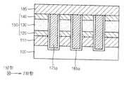
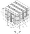
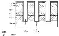
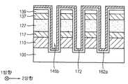
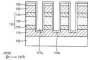
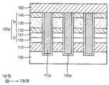
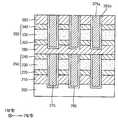
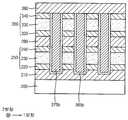
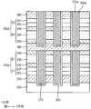
도 1 내지 도 3b는 예시적인 실시예들에 따른 가변 저항 메모리 장치를 설명하기 위한 사시도, 평면도 및 단면도들이다. 구체적으로, 도 1은 상기 가변 저항 메모리 장치의 사시도이고, 도 2는 상기 가변 저항 메모리 장치의 개략적인 평면도이며, 도 3a 및 3b는 상기 가변 저항 메모리 장치의 단면도들이다.1 to 3B are a perspective view, a plan view, and a cross-sectional view for explaining a variable resistance memory device according to exemplary embodiments. Specifically, FIG. 1 is a perspective view of the variable resistance memory device, FIG. 2 is a schematic plan view of the variable resistance memory device, and FIGS. 3 a and 3 b are cross-sectional views of the variable resistance memory device.
도 1 내지 도 3b는 도전 라인들이 교차하는 교차부에 하나의 가변 저항 소자가 구비되는 크로스-포인트(cross-point) 셀 어레이 구조를 갖는 가변 저항 메모리 장치를 도시하고 있다. 설명의 편의를 위해, 도 2에서는 제1 도전 라인, 제2 도전 라인, 메모리 셀 및 열 장벽막 패턴 구조물 만을 도시하였으며, 기타 절연성 구조물의 도시는 생략되었다.1 to 3B show a variable resistance memory device having a cross-point cell array structure in which one variable resistance element is provided at an intersection at which the conductive lines cross each other. For convenience of explanation, only the first conductive line, the second conductive line, the memory cell and the thermal barrier film pattern structure are shown in FIG. 2, and the illustration of other insulating structures is omitted.
도 1 내지 도 3b를 참조하면, 상기 가변 저항 메모리 장치는 베이스절연막(100) 상에 형성된 제1 도전 라인(110), 제2 도전 라인(180), 메모리 셀(150) 및 열 장벽막 패턴 구조물(thermal barrier layer pattern structure)을 포함할 수 있다.1 to 3B, the variable resistance memory device includes a first
예시적인 실시예들에 있어서, 제1 및 제2 도전 라인들(110, 180)은 각각 복수 개로 형성될 수 있으며, 이들이 서로 교차하는 각 교차부(160)에 메모리 셀(150)이 형성될 수 있다.In exemplary embodiments, the first and second
베이스 절연막(100)은 실리콘 산화물, 실리콘 질화물 또는 실리콘 산질화물과 같은 절연 물질을 포함할 수 있다. 베이스 절연막(100)은 기판(도시되지 않음) 상에 형성된 트랜지스터와 같은 하부 구조물(도시되지 않음)을 커버할 수 있다.The base
제1 도전 라인(110)은 베이스 절연막(100) 상면에 대해 평행한 제1 방향을 따라 연장될 수 있으며, 베이스 절연막(100) 상면에 대해 평행하며 상기 제1 방향과 교차하는 제2 방향을 따라 복수 개로 배치될 수 있다.The first
예시적인 실시예들에 있어서, 상기 제1 방향 및 상기 제2 방향은 실질적으로 서로 수직할 수 있다. 다른 실시예들에 있어서, 상기 제1 방향 및 상기 제2 방향은 서로 예각을 가질 수도 있다. 이하 모든 도면들에서, 상기 제1 방향 및 상기 제2 방향의 정의는 동일하다.In the exemplary embodiments, the first direction and the second direction may be substantially perpendicular to each other. In other embodiments, the first direction and the second direction may have an acute angle with each other. In all the following figures, the definitions of the first direction and the second direction are the same.
제1 도전 라인(110)은 예를 들어, 텅스텐(W), 구리(Cu), 알루미늄(Al), 티타늄(Ti) 또는 탄탈륨(Ta)과 같은 금속을 포함할 수 있다. 예시적인 실시예들에 있어서, 제1 도전 라인(110)은 상기 가변 저항 메모리 장치의 비트 라인(bit line) 또는 워드 라인(word line)으로 제공될 수 있다.The first
제2 도전 라인(180)은 상기 제2 방향으로 연장될 수 있으며, 상기 제1 방향을 따라 복수 개로 배치될 수 있다.The second
제2 도전 라인(180)은 예를 들어, 텅스텐, 구리, 알루미늄, 티타늄 또는 탄탈륨과 같은 금속을 포함할 수 있다. 예시적인 실시예들에 있어서, 제1 도전 라인(110)이 비트 라인으로 제공되는 경우 제2 도전 라인(180)은 워드 라인으로 제공될 수 있으며, 제1 도전 라인(110)이 워드 라인으로 제공되는 경우 제2 도전 라인(180)은 비트 라인으로 제공될 수 있다.The second
제1 및 제2 도전 라인들(110, 180)이 각각 복수 개로 형성됨에 따라 이들의 각 교차부(160)에 형성되는 메모리 셀(150) 역시 복수 개로 형성될 수 있다. 이에 따라, 상기 제1 방향을 따라 복수 개로 배치된 메모리 셀들(150)은 메모리 셀 열(column)을 정의할 수 있고, 상기 제2 방향을 따라 복수 개로 배치된 메모리 셀들(150)은 메모리 셀 행(row)을 정의할 수 있다.The first and second
메모리 셀(150)은 가변 저항층(130)을 포함할 수 있다.The
예시적인 실시예들에 있어서, 가변 저항층(130)은 산소 베이컨시(oxygen vacancy) 혹은 산소 이동에 의해 전기 저항이 변화하는 물질을 포함할 수 있으며, 이에 따라 상기 가변 저항 메모리 장치는 저항 변화 메모리(ReRAM) 장치일 수 있다.In the exemplary embodiments, the
예를 들어, 가변 저항층(130)은 페로브스카이트(perovskite) 계열의 물질 또는 전이 금속 산화물을 포함할 수 있다. 상기 페로브스카이트 계열 물질의 예로서, STO(SrTiO3), BTO(BaTiO3), PCMO(Pr1-XCaXMnO3) 등을 들 수 있다. 상기 전이 금속 산화물의 예로서, 티타늄 산화물(TiOx), 지르코늄 산화물(ZrOx), 알루미늄 산화물(AlOx), 하프늄 산화물(HfOx), 탄탈륨 산화물(TaOx), 니오븀 산화물(NbOx), 코발트 산화물(CoOx), 텅스텐 산화물(WOx), 란탄 산화물(LaOx), 아연 산화물(ZnOx) 등을 포함할 수 있다. 이들은 단독으로 혹은 2 이상이 조합되어 사용될 수 있다.For example, the
예시적인 실시예들에 있어서, 가변 저항층(130)은 상술한 물질을 포함하는 복수 개의 막이 적층된 구조를 가질 수 있다. 예를 들어, 가변 저항층(130)은 제1 하프늄 산화물(HfO2) 막, 제2 하프늄 산화물(HfOx) 막 및 지르코늄 산화물 막이 적층된 구조를 가질 수 있다. 또한, 가변 저항층(130)은 티타늄 알루미늄 산화물(TiAlOx) 막, 탄탄륨 산화물 막 및 알루미늄 산화물 막이 적층된 구조를 가질 수도 있다.In the exemplary embodiments, the
예시적인 실시예들에 있어서, 가변 저항층(130)은 상변화에 따라 저항이 변하는 물질을 포함할 수 있으며, 이에 따라 상기 가변 저항 메모리 장치는 상변화 메모리(PRAM) 장치일 수 있다. 예를 들어, 가변 저항층(130)은 게르마늄(Ge), 안티몬(Sb) 및/또는 텔루륨(Te)이 소정의 비율로 조합된 칼코게나이드(chalcogenide) 계열의 물질을 포함할 수 있다.In the exemplary embodiments, the variable
예시적인 실시예들에 있어서, 가변 저항층(130)은 자기장 또는 스핀 전달 토크(Spin Transfer Torque: STT)에 의해 저항이 변하는 물질을 포함할 수 있으며, 이에 따라 상기 가변 저항 메모리 장치는 자기 메모리(MRAM) 장치일 수 있다. 예를 들어, 가변 저항층(130)은 철(Fe), 니켈(Ni), 코발트(Co), 디스프로슘(Dy), 가돌리늄(Gd) 등을 포함하는 강자성체를 포함할 수 있다.In the exemplary embodiments, the
예시적인 실시예들에 있어서, 메모리 셀(150)은 제1 도전 라인(110)과 가변 저항층(130) 사이에 배치되는 하부 전극(120) 및 제2 도전 라인(180)과 가변 저항층(130) 사이에 배치되는 상부 전극(140)을 더 포함할 수 있다.In the exemplary embodiments, the
하부 전극(120) 및 상부 전극(140)은 예를 들어, 티타늄 질화물(TiNx), 티타늄 실리콘 질화물(TiSiNx), 텅스텐 질화물(WNx), 텅스텐 실리콘 질화물(WSiNx), 탄탈륨 질화물(TaNx), 탄탈륨 실리콘 질화물(TaSiNx), 지르코늄 질화물(ZrNx), 지르코늄 실리콘 질화물(ZrSiNx) 등과 같은 금속 질화물 또는 금속 실리콘 질화물을 각각 포함할 수 있다.The
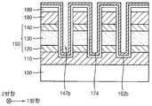
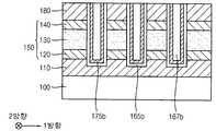
상기 열 장벽막 패턴 구조물은 메모리 셀들(150) 사이에 형성될 수 있다. 예시적인 실시예들에 있어서, 상기 열 장벽막 패턴 구조물은 제1 열 장벽막 패턴(175a) 및 제2 열 장벽막 패턴(175b)을 포함할 수 있다.The thermal barrier film pattern structure may be formed between
제1 열 장벽막 패턴(175a)은 인접하는 상기 메모리 셀 열들 사이에 형성되어, 상기 제1 방향을 따라 연장될 수 있다. 도 3a에 도시된 바와 같이, 제1 열 장벽막 패턴(175a)에 의해 제1 도전 라인들(110)이 서로 구분 혹은 분리될 수 있다. 예시적인 실시예들에 있어서, 제1 열 장벽막 패턴(175a)은 베이스 절연막(100) 내부로도 연장되어 하부가 베이스 절연막(100)에 의해 둘러싸일 수 있다.The first thermal
제2 열 장벽막 패턴(175b)은 인접하는 상기 메모리 셀 행들 사이에 형성되어, 상기 제2 방향을 따라 연장될 수 있다. 도 3b에 도시된 바와 같이, 제2 열 장벽막 패턴(175b)에 의해 제2 도전 라인들(180)이 서로 구분 혹은 분리될 수 있다. 예시적인 실시예들에 있어서, 제2 열 장벽막 패턴(175b)은 제1 도전 라인(110) 내부로도 연장되어 하부가 제1 도전 라인(110)에 의해 둘러싸일 수 있다.The second thermal
도 3a 및 도 3b에 도시된 바와 같이, 메모리 셀(150)의 측벽 상에는 절연막 패턴 구조물이 형성될 수 있다. 예시적인 실시예들에 있어서, 상기 절연막 패턴 구조물은 제1 열 장벽막 패턴(175a)을 감싸는 제1 절연막 패턴(165a) 및 제2 열 장벽막 패턴(175b)을 감싸는 제2 절연막 패턴(165b)을 포함할 수 있다. 상기 절연막 패턴 구조물은 예를 들어, 실리콘 산화물 또는 실리콘 질화물과 같은 절연 물질을 포함할 수 있다.As shown in FIGS. 3A and 3B, an insulating film pattern structure may be formed on the sidewalls of the
제1 절연막 패턴(165a) 및 제2 절연막 패턴(165b)은 각각 제1 열 장벽막 패턴(175a)과 제2 열 장벽막 패턴(175b)의 측벽 및 저면을 커버할 수 있다. 이에 따라, 제1 절연막 패턴(165a)은 메모리 셀(150)의 측벽 및 제1 도전 라인(110)의 측벽 상에 형성될 수 있다. 또한, 제2 절연막 패턴(165b)은 메모리 셀(150)의 측벽 및 제2 도전 라인(180)의 측벽 상에 형성될 수 있다. 또한, 제1 및 제2 열 장벽막 패턴들(175a, 175b)은 각각 제1 및 제2 절연막 패턴들(165a, 165b)에 의해 인접한 메모리 셀들(150)로부터 이격될 수 있다.The first insulating
예시적인 실시예들에 있어서, 제1 및 제2 열 장벽막 패턴들(175a, 175b)은 제1 및 제2 절연막 패턴들(165a, 165b)이 포함하는 물질보다 열 전도도가 낮은 물질을 포함할 수 있다. 일 실시예에 있어서, 제1 및 제2 절연막 패턴들(165a, 165b)이 실리콘 산화물을 포함하는 경우, 제1 및 제2 열 장벽막 패턴들(175a, 175b)은 실리콘 산화물보다 열 전도도가 낮은 물질을 포함하도록 형성될 수 있다. 제1 및 제2 열 장벽막 패턴들(175a, 175b)은, 예를 들어 열 전도도가 1W/m K 보다 낮은 물질인 GST, 다공성 실리콘 산화물, 폴리이미드, 텅스텐 셀레늄(WSe2) 등을 포함할 수 있으며, 이들은 단독으로 또는 2 이상 조합되어 사용될 수 있다.In the exemplary embodiments, the first and second thermal
예시적인 실시예들에 있어서, 상기 가변 저항 메모리 장치는 인접하는 메모리 셀들(150) 사이로 서로 교차하는 제1 및 제2 절연막 패턴들(165a, 165b)을 포함할 수 있으며, 제1 및 제2 절연막 패턴들(165a, 165b)에 의해 둘러싸이는 제1 및 제2 열 장벽막 패턴들(175a, 175b)을 포함할 수 있다. 이에 따라, 인접하는 메모리 셀들(150)은 순차적으로 적층된 제1 절연막 패턴(165a) 및 제1 열 장벽막 패턴(175a)과, 역시 순차적으로 적층된 제2 절연막 패턴(165b) 및 제2 열 장벽막 패턴(175b)에 의해 둘러싸일 수 있다.In the exemplary embodiments, the variable resistance memory device may include first and second
상기 가변 저항 메모리 장치를 동작시키기 위해 전압을 가할 때, 메모리 셀(150) 내에서 열이 발생하여 인접하는 메모리 셀들(150) 사이에 열이 전달되어 상기 가변 저항 메모리 장치가 열화될 수 있다. 하지만 예시적인 실시예들에 따른 상기 가변 저항 메모리 장치는 열 전도도가 낮은 물질을 포함하는 제1 및 제2 열 장벽막 패턴들(175a, 175b)이 메모리 셀들(150)을 둘러싸므로, 이들 사이의 열 전달이 감소될 수 있으며, 이에 따라 동작 신뢰성이 향상될 수 있다.When a voltage is applied to operate the variable resistance memory device, heat is generated in the
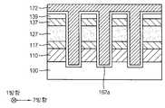
도 4 내지 도 13은 예시적인 실시예들에 따른 가변 저항 메모리 장치의 제조 방법을 설명하기 위한 단면도 및 평면도들이다. 구체적으로, 도 4, 도 5a, 도 6, 도 7, 도 8 및 도 9a는 상기 제2 방향으로의 단면도들이고, 도 9b, 도 10a, 도 11, 도 12 및 도 13은 상기 제1 방향으로의 단면도들이며, 도 5b 및 도 10b는 평면도들이다.FIGS. 4 to 13 are cross-sectional views and plan views for explaining a method of manufacturing a variable resistance memory device according to exemplary embodiments. Specifically, Figs. 4, 5A, 6, 7, 8 and 9A are sectional views in the second direction, and Figs. 9B, 10A, 11, 12, And Figs. 5B and 10B are plan views.
도 4를 참조하면, 베이스 절연막(100) 상에 제1 도전막(112), 하부 전극막(113), 가변 저항 물질막(123) 및 상부 전극막(133)을 순차적으로 형성한다.Referring to FIG. 4, a first
베이스 절연막(100)은 예를 들어, 실리콘 산화물, 실리콘 질화물 또는 실리콘 산질화물과 같은 절연 물질을 포함할 수 있다. 베이스 절연막(100)은 기판(도시되지 않음) 상에 형성된 하부 구조물(도시되지 않음)을 커버할 수 있다. 상기 하부 구조물은 예를 들어, 트랜지스터일 수 있다.The base
제1 도전막(112)은 예를 들어, 텅스텐, 구리, 알루미늄, 티타늄 또는 탄탈륨과 같은 금속을 사용하여 형성될 수 있다. 이들은 단독으로 혹은 2 이상을 조합하여 사용될 수 있다.The first
하부 전극막(113) 및 상부 전극막(133)은 금속 질화물 또는 금속 실리콘 질화물을 사용하여 형성될 수 있다. 예를 들어, 하부 전극막(113) 및 상부 전극막(133)은 티타늄 질화물, 티타늄 실리콘 질화물, 텅스텐 질화물, 텅스텐 실리콘 질화물, 탄탈륨 질화물, 탄탈륨 실리콘 질화물, 지르코늄 질화물 또는 지르코늄 실리콘 질화물을 사용하여 형성될 수 있다. 이들은 단독으로 또는 2 이상을 조합되어 사용될 수 있다.The
가변 저항 물질막(123)은 상기 가변 저항 메모리 장치의 종류에 따라 적절한 물질을 사용하여 형성될 수 있다. 예시적인 실시예들에 있어서, 상기 가변 저항 메모리 장치가 ReRAM 장치인 경우, 가변 저항 물질막(123)은 페로브스카이트 계열 물질 또는 전이 금속 산화물을 사용하여 형성될 수 있다. 이 경우, 가변 저항 물질막(123)은 예를 들어, STO, BTO, PCMO, 티타늄 산화물, 지르코늄 산화물, 알루미늄 산화물, 하프늄 산화물, 탄탈륨 산화물, 니오븀 산화물, 코발트 산화물, 텅스텐 산화물, 란탄 산화물, 아연 산화물 등을 사용하여 형성될 수 있다. 이들은 단독으로 혹은 2 이상이 조합되어 사용될 수 있다. 가변 저항 물질막(123)은 상술한 물질을 함유하는 복수 개의 막들이 적층된 구조로 형성될 수도 있다The variable
예시적인 실시예들에 있어서, 상기 가변 저항 메모리 장치가 PRAM 장치인 경우, 가변 저항 물질막(123)은 칼코게나이드 계열의 물질을 사용하여 형성될 수 있다. 이와는 달리, 상기 가변 저항 메모리 장치가 MRAM 장치인 경우, 가변 저항 물질막(123)은 예를 들어, 철, 니켈, 코발트, 디스프로슘, 가돌리늄 등을 포함하는 강자성체를 사용하여 형성될 수 있다.In the exemplary embodiments, when the variable resistive memory device is a PRAM device, the variable
제1 도전막(112), 하부 전극막(113), 가변 저항 물질막(123) 및 상부 전극막(133)은 예를 들어, 물리 기상 증착(Physical Vapor Deposition: PVD) 공정, 스퍼터링(sputtering) 공정, 원자층 증착(Atomic Layer Deposition: ALD) 공정 또는 화학 기상 증착(Chemical Vapor Deposition: CVD) 공정을 수행하여 형성될 수 있다.The first
도 5a 및 도 5b를 참조하면, 상부 전극막(133), 가변 저항 물질막(123), 하부 전극막(113) 및 제1 도전막(112)을 관통하여 베이스 절연막(100)을 노출하는 제1 트렌치(145)를 형성한다.5A and 5B, the
예시적인 실시예들에 있어서, 상부 전극막(133) 상에 상부 전극막(133) 상면을 부분적으로 노출시키며 상기 제1 방향으로 연장되는 제1 마스크(139)를 형성한 후, 제1 마스크(139)를 이용한 건식 식각 공정을 통해 상부 전극막(133), 가변 저항 물질막(123), 하부 전극막(113) 및 제1 도전막(112)을 관통하는 제1 트렌치(145)를 형성할 수 있다. 제1 마스크(139)는 예를 들어, 실리콘 질화물을 이용하여 형성할 수 있다.In the exemplary embodiments, after forming the
한편, 제1 트렌치(145)를 형성하기 위한 상기 식각 공정에 의해 베이스 절연막(100)의 상부가 과도 식각될 수 있다.Meanwhile, the upper portion of the
예시적인 실시예들에 있어서, 제1 트렌치(145)는 상기 제1 방향을 따라 연장되며, 상기 제2 방향을 따라 복수 개로 형성될 수 있다. 한편, 제1 트렌치(145)가 형성됨에 따라, 베이스 절연막(100) 상에 순차적으로 적층되어 상기 제1 방향을 따라 연장되는 제1 도전 라인(110), 하부 전극막 패턴(117), 가변 저항 물질막 패턴(127) 및 상부 전극막 패턴(137)이 형성될 수 있다.In the exemplary embodiments, the
상술한 바와 같이, 제1 트렌치(145)는 베이스 절연막(100) 일부까지 관통하도록 형성되므로, 서로 분리된 복수 개의 제1 도전 라인들(110)이 형성될 수 있다. 제1 도전막(112) 식각 공정 시, 베이스 절연막(100) 상면의 식각 잔류물에 의해 인접하는 제1 도전 라인들(110) 사이에서 크로스-토크와 같은 간섭 현상이 발생할 수 있다. 하지만 예시적인 실시예들에 있어서, 제1 트렌치(145) 형성을 위한 식각 공정 시, 베이스 절연막(100) 상부가 과도 식각됨으로써 상기 식각 잔류물이 제거될 수 있다. 이에 따라, 제1 도전 라인(110)을 통한 신호 전달의 신뢰성이 증가될 수 있다.As described above, since the
제1 도전 라인(110)은 상기 가변 저항 메모리 장치의 비트 라인 또는 워드 라인으로 제공될 수 있다.The first
도 6을 참조하면, 제1 트렌치(145)의 측벽 및 저면과 제1 마스크(139) 상에 제1 절연막(162)을 형성할 수 있다.Referring to FIG. 6, a first insulating layer 162 may be formed on the sidewalls and bottom surfaces of the
구체적으로, 제1 트렌치(145)의 상기 측벽 및 저면 및 제1 마스크(139) 상에 제1 절연막(162a)을 형성한다. 제1 절연막(162a)은 예를 들어, 실리콘 질화물 또는 실리콘 산화물 등과 같은 절연 물질을 사용하여 CVD 공정 또는 ALD 공정을 통해 형성할 수 있다.Specifically, a first
도 7을 참조하면, 제1 절연막(162a) 상에 제1 열 장벽막(172)을 형성한다.Referring to FIG. 7, a first
제1 열 장벽막(172)은 CVD 공정 또는 ALD 공정을 통해 형성될 수 있으며, 제1 트렌치(145)를 충분히 채우도록 형성될 수 있다.The first
예시적인 실시예에 있어서, 제1 열 장벽막(172)은 제1 절연막(162a)에 포함된 물질보다 열 전도도가 낮은 물질을 포함하도록 형성될 수 있다. 일 실시예에 있어서, 제1 절연막(162a)이 실리콘 산화물을 포함하는 경우, 제1 열 장벽막(172)은 실리콘 산화물보다 열 전도도가 낮은 물질, 예를 들어, 상변화 물질, 다공성 실리콘 산화물, 폴리이미드, 텅스텐 셀레늄 (WSe2) 등을 포함하도록 형성될 수 있다. 이들은 단독으로 또는 2 이상을 조합하여 사용될 수 있다.In an exemplary embodiment, the first
도 8을 참조하면, 제1 열 장벽막(172) 및 제1 절연막(162a)을 평탄화하여 각각 제1 열 장벽막 패턴(175a) 및 제1 절연막 패턴(165a)을 형성한다.Referring to FIG. 8, the first
구체적으로, 제1 마스크(139)를 연마 정지막으로 사용하여 상부 전극막 패턴(137)의 상면이 노출될 때까지 CMP 공정 및/또는 에치-백 공정을 통해 제1 열 장벽막(172), 제1 절연막(162a) 및 제1 마스크(139)를 평탄화할 수 있다. 이때, 제1 열 장벽막(172) 및 제1 절연막(162a)은 평탄화되어 각각 제1 열 장벽막 패턴(175a) 및 제1 절연막 패턴(165a)을 형성할 수 있으며, 제1 마스크(139)는 완전히 제거될 수 있다. 제1 열 장벽막 패턴(175a) 및 제1 절연막 패턴(165a)은 제1 트렌치(145) 내부에서 상기 제1 방향으로 연장될 수 있다.Specifically, the first
도 9a 및 도 9b를 참조하면, 상부 전극막 패턴(137), 제1 절연막 패턴(165a) 및 제1 열 장벽막 패턴(175a) 상에 제2 도전막(177)을 형성한다.9A and 9B, a second
구체적으로, 제2 도전막(177)은 예를 들어, 텅스텐, 구리, 알루미늄, 티타늄 또는 탄탈륨과 같은 금속을 사용하여 형성할 수 있다. 이들은 단독으로 혹은 2 이상을 조합하여 사용될 수 있다. 제2 도전막(177)은 PVD 공정, 스퍼터링 공정, ALD 공정, CVD 공정 등을 수행하여 형성될 수 있다.Specifically, the second
도 10a 및 도 10b를 참조하면, 도 5를 참조로 설명한 공정과 실질적으로 동일하거나 유사한 공정을 수행함으로써, 제2 도전막(177), 상부 전극막 패턴(137), 가변 저항 물질막 패턴(127) 및 하부 전극막 패턴(117)을 관통하여 제1 도전 라인(110)을 노출하는 제2 트렌치(147)를 형성한다.Referring to FIGS. 10A and 10B, the second
구체적으로, 제2 도전막(177) 상에 제2 도전막(177) 상면을 일부 노출시키고 상기 제2 방향으로 연장되는 제2 마스크(189)를 형성한 후, 제2 마스크(189)를 이용한 식각 공정을 수행하여 제2 도전막(177), 상부 전극막 패턴(137), 가변 저항 물질막 패턴(127) 및 하부 전극막 패턴(117)을 관통하는 제2 트렌치(147)를 형성할 수 있다. 제2 마스크(189)는 예를 들어, 실리콘 질화물을 이용하여 형성할 수 있다. 한편, 제2 트렌치(147)를 형성하기 위한 상기 식각 공정에 의해 제1 도전 라인(110)의 상부가 과도 식각될 수 있다. 또한, 상기 식각 공정 시, 노출된 제1 절연막 패턴(165a) 및 제1 열 장벽막 패턴(175a)의 일부가 함께 제거될 수도 있다. 이에 따라, 제2 트렌치(147)에 의해 서로 이격된 복수 개의 제1 절연막 패턴들(165a) 및 제1 열 장벽막 패턴들(175a)이 형성될 수 있다.Specifically, after the upper surface of the second
예시적인 실시예들에 있어서, 제2 트렌치(147)는 상기 제2 방향을 따라 연장되며, 상기 제1 방향을 따라 복수 개로 형성될 수 있다. 제2 트렌치(147)가 형성됨에 따라, 상기 제1 방향을 따라 연장되는 라인 형상의 하부 전극막 패턴(117), 가변 저항 물질막 패턴(127) 및 상부 전극막 패턴(137)은 각각 실질적으로 고립된 섬(island) 형상을 갖는 하부 전극(120), 가변 저항층(130) 및 상부 전극(140)으로 변환될 수 있다. 하부 전극(120), 가변 저항층(130) 및 상부 전극(140)은 함께 메모리 셀(150)을 형성할 수 있다.In the exemplary embodiments, the
한편, 제2 도전막(177)은 제2 트렌치(147)에 의해 상기 제2 방향으로 각각 연장되며 상기 제1 방향을 따라 복수 개로 형성된 제2 도전 라인들(180)로 변환될 수 있다. 이에 따라, 각 제2 도전 라인들(180)은 제1 도전 라인(110) 상부에서 제1 도전 라인(110)과 서로 교차되거나 혹은 오버랩 될 수 있다. 도 2에 도시된 바와 같이, 제1 도전 라인(110) 및 제2 도전 라인(180)이 교차하는 각 교차부(160)마다 메모리 셀(150)이 형성될 수 있다.The second
예시적인 실시예들에 있어서, 제1 도전 라인(110)이 비트 라인으로 제공되는 경우 제2 도전 라인(180)은 워드 라인으로 제공될 수 있으며, 반대로 제1 도전 라인(110)이 워드 라인으로 제공되는 경우 제2 도전 라인(180)은 비트 라인으로 제공될 수 있다.In the exemplary embodiments, the second
하부 전극막 패턴(117)의 식각 공정 시, 제1 도전 라인(110) 상의 식각 잔류물이 인접하는 메모리 셀들(150) 사이에 크로스-토크와 같은 간섭 현상이 발생시킬 수 있으나, 예시적인 실시예들에 있어서, 제2 트렌치(147) 형성을 위한 식각 공정 시, 제1 도전 라인(110) 상부가 과도 식각됨으로써 상기 식각 잔류물이 함께 제거될 수 있다. 이에 따라, 메모리 셀(150) 동작의 신뢰성이 향상될 수 있다.An etch residue on the first
도 11을 참조하면, 도 6을 참조로 설명한 공정과 실질적으로 동일하거나 유사한 공정을 수행함으로써, 제2 트렌치(147)의 측벽 및 저면과 제2 마스크(189) 상에 제2 절연막(162b)을 형성한다.Referring to FIG. 11, by performing a process substantially the same or similar to the process described with reference to FIG. 6, a second
제2 절연막(162b)은 예를 들어, 실리콘 질화물 또는 실리콘 산화물을 사용하여 CVD 공정 또는 ALD 공정을 통해 형성할 수 있다.The second
도 12를 참조하면, 도 7을 참조로 설명한 공정과 실질적으로 동일하거나 유사한 공정을 수행함으로써, 제2 절연막(162b) 상에 제2 열 장벽막(174)을 형성한다.Referring to FIG. 12, a second
제2 열 장벽막(174)은 CVD 공정 또는 ALD 공정을 통해 제2 절연막(162b) 상에 형성될 수 있으며, 제2 트렌치(147)를 채울 수 있다.The second
예시적인 실시예들에 있어서, 제2 열 장벽막(174)은 제2 절연막(162b)에 포함된 물질보다 열 전도도가 낮은 물질을 포함하도록 형성될 수 있다. 제2 절연막(162b)이 실리콘 산화물을 포함하는 경우, 제2 열 장벽막(174)은 실리콘 산화물보다 열 전도도가 낮은 물질을 포함하도록 형성될 수 있다. 일 실시예에 있어서, 제2 열 장벽막(174)은 제1 열 장벽막(172)과 실질적으로 동일한 물질을 포함하도록 형성할 수 있다.In the exemplary embodiments, the second
도 13을 참조하면, 도 8을 참조로 설명한 공정과 실질적으로 동일하거나 유사한 공정을 수행함으로써, 제2 열 장벽막(174) 및 제2 절연막(162b)을 평탄화하여 각각 제2 열 장벽막 패턴(175b) 및 제2 절연막 패턴(165b)을 형성한다.Referring to FIG. 13, the second
구체적으로, 제2 마스크(189)를 연마 정지막으로 사용하여 제2 도전 라인(180)의 상면이 노출될 때까지 제2 열 장벽막(174)및 제2 절연막(162b)을 CMP 공정 및/또는 에치-백 공정을 통해 평탄화함으로써, 제2 열 장벽막 패턴(175b) 및 제2 절연막 패턴(165b)을 형성할 수 있다. 이때, 제2 마스크(189)는 완전히 제거될 수 있다. 제2 열 장벽막 패턴(175b) 및 제2 절연막 패턴(165b)은 제2 트렌치(147) 내부에서 상기 제2 방향으로 연장될 수 있다.Specifically, the second
예시적인 실시예들에 있어서, 제1 절연막 패턴(165a) 및 제1 열 장벽막 패턴(175a)과 제2 절연막 패턴(165b) 및 제2 열 장벽막 패턴(175b)은 각각 상기 제1 방향 및 상기 제2 방향으로 연장되며 서로 교차할 수 있다. 따라서, 하나의 메모리 셀(150)의 모든 측면은 2개의 제1 절연막 패턴(165a) 및 2개의 제2 절연막 패턴(165b)에 의해 둘러싸일 수 있다.In the exemplary embodiments, the first insulating
예시적인 실시예들에 있어서, 상기 가변 저항 메모리 장치는 상기 절연막 패턴 구조물에 의해 감싸지는 상기 열 장벽막 패턴 구조물을 포함하도록 형성될 수 있다. 상기 열 장벽막 패턴 구조물은 상기 절연막 패턴 구조물보다 열 전도도가 낮은 물질을 포함할 수 있으며, 이에 따라, 상기 열 장벽막 패턴 구조물은 상기 가변 저항 메모리 장치가 동작될 때 발생하는 인접하는 메모리 셀들(150)간의 열 전달을 감소시키므로, 상기 가변 저항 메모리 장치의 신뢰성이 향상될 수 있다.In exemplary embodiments, the variable resistive memory device may be formed to include the thermal barrier film pattern structure that is enclosed by the insulating film pattern structure. The thermal barrier film pattern structure may include a material having a thermal conductivity lower than that of the insulation film pattern structure. Accordingly, the thermal barrier film pattern structure may include adjacent memory cells 150 ), The reliability of the variable resistance memory device can be improved.
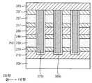
도 14 내지 도 15b는 예시적인 실시예들에 따른 가변 저항 메모리 장치를 설명하기 위한 사시도 및 평면도이다. 구체적으로, 도 14는 상기 가변 항 메모리 장치를 설명하기 위한 사시도이고, 도 15a 및 15b는 상기 가변 저항 메모리 장치를 설명하기 위한 단면도들이다. 상기 가변 저항 메모리 장치는, 상기 절연막 패턴 구조물 및 상기 열 장벽막 패턴 구조물의 형상을 제외하고는 도 1 내지 도 3b를 참조로 한 가변 저항 메모리 장치와 실질적으로 동일하거나 유사하다. 이에 따라, 동일한 구성 요소에는 동일한 참조 부호를 부여하고, 이에 대한 자세한 설명은 생략한다.14 to 15B are a perspective view and a plan view for explaining a variable resistance memory device according to exemplary embodiments. Specifically, Fig. 14 is a perspective view for explaining the variable-resistance memory device, and Figs. 15A and 15B are cross-sectional views for explaining the variable resistance memory device. The variable resistive memory device is substantially the same as or similar to the variable resistive memory device with reference to FIGS. 1 to 3B except for the shapes of the insulating film pattern structure and the thermal barrier film pattern structure. Accordingly, the same components are denoted by the same reference numerals, and a detailed description thereof will be omitted.
도 14 내지 도 15b를 참조하면, 상기 가변 저항 메모리 장치는 베이스 절연막(100) 상에 형성된 제1 도전 라인(110), 제2 도전 라인(180), 메모리 셀(150) 및 열 장벽막 패턴 구조물을 포함할 수 있다.14 to 15B, the variable resistance memory device includes a first
상기 열 장벽막 패턴 구조물은 메모리 셀들(150) 사이에 형성될 수 있다. 예시적인 실시예들에 있어서, 상기 열 장벽막 패턴 구조물은 제1 열 장벽막 패턴(175a) 및 제2 열 장벽막 패턴(175b)을 포함할 수 있다.The thermal barrier film pattern structure may be formed between
제1 열 장벽막 패턴(175a)은 인접하는 메모리 셀 열들 사이에 형성되어, 제1 방향을 따라 연장될 수 있으며, 제2 열 장벽막 패턴(175b)은 인접하는 메모리 셀 행들 사이에 형성되어, 제2 방향을 따라 연장될 수 있다.A first thermal
도 15a 및 15b에 도시된 바와 같이 메모리 셀(150)의 측벽 및 상기 열 장벽막 패턴 구조물 상에는 절연막 패턴 구조물이 형성될 수 있다. 예시적인 실시예들에 있어서, 상기 절연막 패턴 구조물은 제1 열 장벽막 패턴(175a)을 감싸는 제1 절연막 패턴(165a), 제2 열 장벽막 패턴(175b)을 감싸는 제2 절연막 패턴(165b), 제1 열 장벽막 패턴(175a) 상에 형성된 제3 절연막 패턴(167a) 및 제2 열 장벽막 패턴(175b) 상에 형성된 제4 절연막 패턴(167b)을 포함할 수 있다.15A and 15B, an insulating film pattern structure may be formed on the sidewall of the
이에 따라, 인접한 메모리 셀들(150) 사이에 순차적으로 적층된 제1 절연막 패턴(165a), 제1 열 장벽막 패턴(175a) 및 제3 절연막 패턴(167a)을 포함하는 제1 절연 구조물이 정의될 수 있고, 또한 인접한 메모리 셀들(150) 사이에 순차적으로 적층된 제2 절연막 패턴(165b), 제2 열 장벽막 패턴(175b) 및 제4 절연막 패턴(167b)을 포함하는 제2 절연 구조물이 정의될 수 있다.Accordingly, a first insulating structure including a first
제3 및 제4 절연막 패턴들(167a, 167b)은, 예를 들어, 실리콘 산화물 또는 실리콘 질화물 등과 같은 절연 물질을 포함할 수 있다. 예시적인 실시예들에 있어서, 제3 및 제4 절연막 패턴들(167a, 167b)은 각각 상기 제1 및 제2 절연막 패턴들(165a, 165b)과 실질적으로 동일한 물질을 포함할 수 있다.The third and fourth insulating
예시적인 실시예들에 따른 상기 열 장벽막 패턴 구조물이 메모리 셀들(150)을 둘러싸므로, 이들 사이의 열 전달이 감소될 수 있으며 상기 가변 저항 메모리 장치의 동작 신뢰성이 향상될 수 있다.Since the thermal barrier film pattern structure according to the exemplary embodiments encompasses the
도 16 내지 도 21은 예시적인 실시예들에 따른 가변 저항 메모리 장치의 제조 방법을 설명하기 위한 단면도들이다. 구체적으로, 도 16 내지 도 18은 제2 방향으로의 단면도들이고, 도 19 내지 도 21은 상기 제1 방향으로의 단면도들이다. 상기 가변 저항 메모리 장치의 제조 방법은 도 14 내지 도 15b에 도시된 상기 가변 저항 메모리 장치를 제조하기 위해 사용될 수 있으나, 반드시 이에 한정되는 것은 아니다. 한편, 상기 가변 저항 메모리 장치의 제조 방법은 도 4 내지 도 13을 참조로 설명한 가변 저항 메모리 장치의 제조 방법에 포함된 공정들과 실질적으로 동일하거나 유사한 공정들을 포함할 수 있으며, 이에 따라 이에 대한 자세한 설명은 생략한다.FIGS. 16 through 21 are cross-sectional views illustrating a method of manufacturing a variable resistance memory device according to exemplary embodiments. Specifically, Figs. 16 to 18 are sectional views in the second direction, and Figs. 19 to 21 are sectional views in the first direction. The manufacturing method of the variable resistance memory device may be used for manufacturing the variable resistance memory device shown in Figs. 14 to 15B, but is not limited thereto. Meanwhile, the manufacturing method of the variable resistance memory device may include processes substantially identical to or similar to those included in the manufacturing method of the variable resistance memory device described with reference to FIGS. 4 to 13, The description is omitted.
도 16을 참조하면, 도 4 내지 도 6을 참조로 설명한 공정들과 실질적으로 동일하거나 유사한 공정을 수행한다. 이에 따라, 상부 전극막(133), 가변 저항 물질막(123) 및 하부 전극막(113)을 관통하는 제1 트렌치(145a)를 형성한 후, 제1 트렌치(145a)의 측벽 및 저면과 제1 마스크(139) 상에 제1 절연막(162a)을 형성할 수 있다.Referring to FIG. 16, a process substantially identical to or similar to the processes described with reference to FIGS. Thus, after the
도 17을 참조하면, 도 7 및 도 8을 참조로 설명한 공정들과 실질적으로 동일하거나 유사한 공정을 수행한다. 이에 따라, 제1 절연막(162a)상에 제1 열 장벽막(172)을 형성할 수 있다.Referring to FIG. 17, a process substantially identical to or similar to the processes described with reference to FIGS. 7 and 8 is performed. Accordingly, the first
구체적으로, 제1 절연막(162a)을 따라 얇은 두께를 갖도록 제1 열 장벽막(172)을 형성하여, 제1 열 장벽막(172)에 의해 제1 개구(145b)가 정의될 수 있다.Specifically, the first
도 18을 참조하면, 제3 절연막을 제1 열 장벽막(172) 상에 형성한 후 상기 제3 절연막, 제1 열 장벽막(172) 및 제1 절연막(162a)을 평탄화하여, 각각 제3 절연막 패턴(167a), 제1 열 장벽막 패턴(175a) 및 제1 절연막 패턴(165a)을 형성한다.18, a third insulating film is formed on the first
구체적으로, 제1 개구(145b)를 충분히 채우도록 상기 제3 절연막을 제1 열 장벽막(172) 상에 형성한 후, 상부 전극막 패턴(137)의 상면이 노출될 때까지 상기 제3 절연막, 제1 열 장벽막(172), 제1 절연막(162a) 및 제1 마스크(139)를 CMP 공정 및/또는 에치 백 공정 등을 통해 평탄화 할 수 있다. 이때, 제1 마스크(139)는 완전히 제거될 수 있으며, 상기 제3 절연막, 제1 열 장벽막(172) 및 제1 절연막(162a)은 평탄화되어 각각 제3 절연막 패턴(167a), 제1 열 장벽막 패턴(175a) 및 제1 절연막 패턴(165a)을 형성할 수 있다.Specifically, after the third insulating film is formed on the first
제3 절연막 패턴(167a), 제1 열 장벽막 패턴(175a) 및 제1 절연막 패턴(165a)은 제1 트렌치(145b) 내부에서 상기 제1 방향으로 연장되도록 형성될 수 있다. 상기 제3 절연막은, 예를 들어, 실리콘 산화물 또는 실리콘 질화물 등과 같은 절연물질을 포함할 수 있으며, 상기 제1 절연막과 실질적으로 동일한 물질을 포함하도록 형성될 수 있다.The third
이후, 도 9a 및 도 9b를 참조로 설명한 공정과 실질적으로 동일하거나 유사한 공정을 수행하여, 상부 전극막 패턴(137), 제1 절연막 패턴(165a), 제1 열 장벽막 패턴(175a) 및 제3 절연막 패턴(167b) 상에 제2 도전막(177)을 형성한다.Thereafter, a process substantially identical to or similar to the process described with reference to FIGS. 9A and 9B is performed to form the upper
도 19를 참조하면, 도 10a 내지 도 11을 참조로 설명한 공정들과 실질적으로 동일하거나 유사한 공정을 수행한다. 이에 따라, 제2 트렌치(147a)의 측벽 및 저면과 제2 마스크(189) 상에 제2 절연막(162b)을 형성한다.Referring to Fig. 19, a process substantially identical to or similar to the processes described with reference to Figs. 10A to 11 is performed. Thus, a second
구체적으로, 제2 마스크(189)를 이용한 건식 식각 공정을 통해 제2 도전막(177), 상부 전극막 패턴(137), 가변 저항 물질막 패턴(127) 및 하부 전극막 패턴(117)을 관통하는 제2 트렌치(147a)를 형성한다. 제2 트렌치(147a)가 형성됨에 따라 제1 도전 라인(110)에 순차적으로 적층되며 상기 제2 방향으로 연장되는 제2 도전 라인(180), 상부 전극(140), 가변 저항층(130) 및 하부 전극(120)을 형성할 수 있다. 이후, 제2 트렌치(147a)의 측벽 및 저면과 제2 마스크(189) 상에 제2 절연막(162b)을 형성할 수 있다.Specifically, the second
도 20을 참조하면, 도 12 내지 도 13을 참조로 설명한 공정들과 실질적으로 동일하거나 유사한 공정을 수행한다. 이에 따라 제2 절연막(162b) 상에 제2 열 장벽막(174)을 형성할 수 있다.Referring to FIG. 20, a process substantially identical to or similar to the processes described with reference to FIGS. 12 to 13 is performed. Accordingly, the second
구체적으로, 제2 절연막(162b)의 상면을 따라 얇은 두께를 갖도록 제2 열 장벽막(174)을 형성하여, 제2 열 장벽막(174)에 의해 제2 개구(147b)가 정의될 수 있다.Specifically, the second
도 21을 참조하면, 도 18을 참조로 설명한 공정과 실질적으로 동일하거나 유사한 공정을 수행함으로써, 제4 절연막 패턴(167b), 제2 열 장벽막 패턴(175b) 및 제2 절연막 패턴(165b)을 형성한다.Referring to FIG. 21, the fourth insulating
구체적으로, 제2 개구(147b)를 채우도록 제4 절연막을 제2 열 장벽막(174) 상에 형성한 후, 제2 도전 라인(180)의 상기 상면이 노출될 때까지 상기 제4 절연막, 제2 열 장벽막(174) 및 제2 절연막(162b)을 CMP 공정 및/또는 에치 백 공정 등을 통해 평탄화할 수 있다. 상기 제4 절연막, 제2 열 장벽막(174) 및 제2 절연막(162b)은 평탄화되어 각각 제4 절연막 패턴(167b), 제2 열 장벽막 패턴(175b) 및 제2 절연막 패턴(165b)을 형성할 수 있으며, 이때 제2 마스크(180)는 제거될 수 있다. 제4 절연막 패턴(167b), 제2 열 장벽막 패턴(175b) 및 제2 절연막 패턴(165b)은 상기 제2 방향으로 연장될 수 있다. 상기 제4 절연막은, 예를 들어, 실리콘 산화물 또는 실리콘 질화물 등과 같은 절연물질을 포함할 수 있으며, 상기 제2 절연막과 실질적으로 동일한 물질을 포함할 수 있다.Specifically, a fourth insulating film is formed on the second
예시적인 실시예들에 따른 제1 및 제2 열 장벽막 패턴들(175a, 175b)은 제1 내지 제4 절연막 패턴들(165a, 165b, 167a, 167b)보다 열 전도도가 낮은 물질을 포함할 수 있다. 이에 따라, 제1 및 제2 열 장벽막 패턴들(175a, 175b)은 인접하는 메모리 셀들(150) 간의 열의 전달을 감소시킬 수 있으므로 메모리 셀들(150)을 포함하는 상기 가변 저항 메모리 장치의 동작 신뢰성이 향상될 수 있다.The first and second thermal
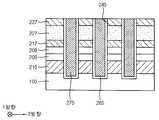
도 22a 및 도 22b는 예시적인 실시예들에 따른 가변 저항 메모리 장치를 나타내는 단면도들이다. 구체적으로, 도 22a 및 도 22b는 각각 상기 가변 저항 메모리 장치의 상기 제2 방향 및 상기 제1 방향으로의 단면도들이다.22A and 22B are cross-sectional views illustrating a variable resistance memory device according to exemplary embodiments. Specifically, Figs. 22A and 22B are sectional views of the variable resistive memory device in the second direction and the first direction, respectively.
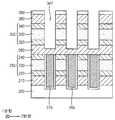
도 22a 내지 도 22b는 도전 라인들이 교차되는 교차부에 하나의 선택 소자 및 하나의 가변 저항 소자가 구비되는 크로스-포인트 셀 어레이 구조를 갖는 가변 저항 메모리 장치를 도시하고 있다. 상기 가변 저항 메모리 장치는 선택 소자를 제외하고는 도 1 내지 도 3b를 참조로 한 가변 저항 메모리 장치와 실질적으로 동일하거나 유사하다. 이에 따라, 동일한 구성 요소에는 동일한 참조 부호를 부여하고, 이에 대한 자세한 설명은 생략한다.FIGS. 22A and 22B show a variable resistance memory device having a cross-point cell array structure in which one selection element and one variable resistance element are provided at intersections where the conductive lines intersect. The variable resistive memory device is substantially the same as or similar to the variable resistive memory device with reference to Figs. 1 to 3B, except for the selection element. Accordingly, the same components are denoted by the same reference numerals, and a detailed description thereof will be omitted.
도 22a 및 도 22b를 참조하면, 상기 가변 저항 메모리 장치는 제1 도전 라인(110), 제2 도전 라인(180), 메모리 셀(150a) 및 열 장벽막 패턴 구조물을 포함할 수 있다.22A and 22B, the variable resistance memory device may include a first
예시적인 실시예들에 있어서, 서로 교차 또는 오버랩 되는 제1 도전 라인(110) 및 제2 도전 라인(180) 사이의 교차부에는 메모리 셀(150a)이 형성될 수 있으며, 메모리 셀(150a)은 순차적으로 적층된 선택 소자(S) 및 가변 저항 소자(R)를 포함할 수 있다.In the exemplary embodiments, a
가변 저항 소자(R)는 하부 전극(120), 가변 저항층(130) 및 상부 전극(140)을 포함할 수 있다.The variable resistance element R may include a
예시적인 실시예들에 있어서, 선택 소자(S)는 P-N 다이오드일 수 있다. 이 경우, 선택 소자(S)는 제1 도전 라인(110) 상에 적층된 하부 반도체층 패턴(105) 및 상부 반도체층 패턴(107)을 포함할 수 있다. 예를 들어, 하부 반도체층 패턴(105) 및 상부 반도체층 패턴(107)은 각각 n형 불순물 및 p형 불순물을 포함하는 폴리실리콘을 포함할 수 있다. 일 실시예에 있어서, 선택 소자(S)는 하부 반도체 층 패턴(105) 및 상부 반도체 층 패턴(107) 사이에 형성된 절연 패턴(도시되지 않음)을 더 포함할 수 있으며, 이 경우 선택 소자(S)는 P-I-N 다이오드일 수 있다.In the exemplary embodiments, the selection element S may be a P-N diode. In this case, the selection element S may include a lower
이와는 달리, 하부 반도체층 패턴(105) 및 상부 반도체층 패턴(107)은 각각 n형 산화물 반도체 및 p형 산화물 반도체를 포함할 수도 있다. 상기 n형 반도체 산화물은 예를 들어, 아연 산화물(ZnOx) 또는 인듐-아연 산화물(InZnOx)을 포함할 수 있으며, 상기 p형 산화물 반도체는 예를 들어, 구리 산화물(CuOx)을 포함할 수 있다.Alternatively, the lower
일 실시예에 있어서, 제1 도전 라인(110) 및 선택 소자(S) 사이에는 제1 버퍼층(도시되지 않음)이 형성될 수 있으며, 선택 소자(S) 및 가변 저항 소자(R) 사이에는 제2 버퍼층(도시되지 않음)이 형성될 수 있다. 상기 제1 및 제2 버퍼층들은 각각 티타늄 질화물, 탄탈륨 질화물, 텅스텐 질화물, 지르코늄 질화물과 같은 금속 질화물을 포함할 수 있다.In one embodiment, a first buffer layer (not shown) may be formed between the first
상기 열 장벽막 패턴 구조물은 제1 열 장벽막 패턴(175a) 및 제2 열 장벽막 패턴(175b)를 포함할 수 있다. 제1 및 제2 열 장벽막 패턴들(175a, 175b)은 메모리 셀들(150a) 사이에서 각각 상기 제1 및 제2 방향으로 연장될 수 있다.The thermal barrier film pattern structure may include a first thermal
메모리 셀(150)의 측벽 상에는 절연막 패턴 구조물이 형성될 수 있다. 예시적인 실시예들에 있어서, 상기 절연막 패턴 구조물은 제1 열 장벽막 패턴(175a)을 감싸는 제1 절연막 패턴(165a) 및 제2 열 장벽막 패턴(175b)을 감싸는 제2 절연막 패턴(165b)을 포함할 수 있다.An insulating film pattern structure may be formed on the sidewalls of the
제1 절연막 패턴(165a) 및 제1 열 장벽막 패턴(175a)은 각각 베이스 절연막(100)으로 연장되어 하부가 베이스 절연막(100)에 의해 둘러싸일 수 있으며, 제2 절연막 패턴(165b) 및 제2 열 장벽막 패턴(175b)은 각각 제1 도전 라인(110)으로 연장되어 하부가 제1 도전 라인(100)에 의해 둘러싸일 수 있다.The first
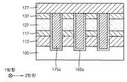
도 23 내지 도 27은 일 실시예에 따른 가변 저항 메모리 장치의 제조 방법을 설명하기 위한 단면도들이다. 구체적으로, 도 23 내지 도 25는 상기 제2 방향으로의 단면도들이다. 상기 가변 저항 메모리 장치의 제조 방법은 도 14 내지 도 15b에 도시된 가변 저항 메모리 장치를 제조하기 위해 사용될 수 있으나, 반드시 이에 한정되는 것은 아니다. 한편, 상기 가변 저항 메모리 장치의 제조 방법은 도 4 내지 도 13을 참조로 설명한 가변 저항 메모리 장치의 제조 방법에 포함된 공정들과 실질적으로 동일하거나 유사한 공정들을 포함할 수 있으며, 이에 따라 이에 대한 자세한 설명은 생략한다.23 to 27 are cross-sectional views illustrating a method of manufacturing a variable resistance memory device according to an embodiment. Specifically, Figs. 23 to 25 are sectional views in the second direction. The method of manufacturing the variable resistance memory device can be used for manufacturing the variable resistance memory device shown in Figs. 14 to 15B, but is not limited thereto. Meanwhile, the manufacturing method of the variable resistance memory device may include processes substantially identical to or similar to those included in the manufacturing method of the variable resistance memory device described with reference to FIGS. 4 to 13, The description is omitted.
도 23을 참조하면, 베이스 절연막(100) 상에 제1 도전막(112), 하부 반도체층(102), 상부 반도체층(104), 하부 전극막(113), 가변 저항 물질막(123) 및 상부 전극막(133)을 순차적으로 형성한다.23, a first
하부 반도체층(102)은 인(P) 혹은 비소(As)와 같은 n형 불순물이 도핑된 폴리실리콘을 이용하여 형성할 수 있다. 하부 반도체층(102)은 비정질 실리콘을 증착한 후, n형 불순물을 도핑하고 예를 들어, 레이저 어닐링과 같은 결정화 공정을 수행하여 형성할 수 있다. 이와는 달리, 하부 반도체층(102)은 아연 산화물 또는 인듐-아연 산화물과 같은 n형 산화물 반도체를 사용하여 형성할 수도 있다.The
상부 반도체층(104)은 붕소(B) 혹은 갈륨(Ga)과 같은 p형 불순물이 도핑된 폴리실리콘을 사용하여 형성할 수 있다. 상부 반도체층(104)은 비정질 실리콘을 증착한 후, p형 불순물을 도핑하고 예를 들어, 레이저 어닐링과 같은 결정화 공정을 수행하여 형성할 수 있다. 이와는 달리, 상부 반도체층(104)은 구리 산화물과 같은 p형 산화물 반도체를 이용하여 형성할 수도 있다.The
하부 반도체층(102) 및 상부 반도체층(104)은 각각 PVD 공정, 스퍼터링 공정, ALD 공정 등을 통해 형성할 수 있다.The
일 실시예에 있어서, 제1 도전막(112) 및 제1 반도체층(102) 사이에 제1 버퍼층(도시되지 않음)을 더 형성할 수 있으며, 제2 반도체층(104) 및 하부 전극막(113) 사이에 제2 버퍼층(도시되지 않음)을 더 형성할 수도 있다. 상기 제1 및 제2 버퍼층들은 각각 티타늄 질화물, 탄탈륨 질화물, 텅스텐 질화물, 지르코늄 질화물과 같은 금속 질화물을 사용하여 PVD 공정, 스퍼터링 공정, ALD 공정 등을 통해 형성될 수 있다.In one embodiment, a first buffer layer (not shown) may be further formed between the first
도 24를 참조하면, 도 5a를 참조로 설명한 공정과 실질적으로 동일하거나 유사한 공정을 수행하여 베이스 절연막(100)의 상부를 노출하는 제1 트렌치(145)를 형성할 수 있다.Referring to FIG. 24, a
제1 트렌치(145)는 상기 제1 방향을 따라 연장되며, 상기 제2 방향으로 복수 개로 형성될 수 있다. 한편, 제1 트렌치(145)를 형성하기 위한 상기 공정에서 베이스 절연막(100)의 상부가 과도 식각될 수 있다.The
제1 트렌치(145)가 형성됨에 따라, 각각 상기 제1 방향으로 연장되며 베이스 절연막(100) 상에 순차적으로 적층되는 제1 도전 라인(110), 하부 반도체층 라인(106), 상부 반도체층 라인(108), 하부 전극막 패턴(117), 가변 저항 물질막 패턴(127) 및 상부 전극막 패턴(137)을 형성할 수 있다.A first
도 25를 참조하면, 도 6 내지 도 8을 참조로 설명한 공정들과 실질적으로 동일하거나 유사한 공정들을 수행할 수 있다.Referring to Fig. 25, it is possible to perform processes substantially the same as or similar to the processes described with reference to Figs.
구체적으로, 제1 트렌치(145)의 측벽 및 저면 상에 제1 절연막 패턴(165a) 및 제1 트렌치(145)의 부분을 채우는 제1 열 장벽막 패턴(175a)을 형성할 수 있다. 제1 절연막 패턴(165a) 및 제1 열 장벽막 패턴(175a) 형성한 이후에 제1 마스크(139)는 제거될 수 있다. 이후, 상부 전극막 패턴(137), 제1 절연막 패턴(165a) 및 제1 열 장벽막 패턴(175a) 상에 제2 도전막(177)을 형성할 수 있다.Specifically, a first thermal
도 26을 참조하면, 도 9a 및 도 9b를 참조로 설명한 공정과 실질적으로 동일하거나 유사한 공정을 수행할 수 있다.Referring to FIG. 26, a process substantially the same as or similar to the process described with reference to FIGS. 9A and 9B can be performed.
이에 따라, 제2 마스크(189)를 식각 마스크로 이용하여 제2 도전막(177), 상부 전극막 패턴(137), 가변 저항 물질막 패턴(127), 하부 전극막 패턴(117), 제2 반도체층 라인(108) 및 제1 반도체층 라인(106)을 관통하며 상기 제2 방향으로 연장되는 제2 트렌치(147)를 형성할 수 있다. 제2 트렌치(147)는 상기 제1 방향을 따라 복수 개로 형성될 수 있다. 또한, 제2 트렌치(147)를 형성하는 상기 공정에서, 제1 도전 라인(110) 상부가 과도 식각될 수 있다.Thus, the second
제2 트렌치(147)가 형성됨에 따라, 상기 제2 방향으로 연장되는 제2 도전 라인(180)이 형성되며, 상부 전극막 패턴(137), 가변 저항 물질막 패턴(127), 하부 전극막 패턴(117), 제2 반도체층 라인(108) 및 제1 반도체층 라인(106)은 각각 상부 전극(140), 가변 저항층(130), 하부 전극(120), 상부 반도체층 패턴(107) 및 하부 반도체층 패턴(105)으로 변환될 수 있다.The second
이에 따라, 하부 전극(120), 가변 저항층(130) 및 상부 전극(140)을 포함하는 가변 저항 소자(R), 하부 반도체층 패턴(105) 및 상부 반도체층 패턴(107)을 포함하는 선택 소자(S)를 형성할 수 있다. 제1 도전 라인(110) 및 제2 도전 라인(180)의 교차부에는 순차적으로 적층된 선택 소자(S) 및 가변 저항 소자(R)를 포함하는 메모리 셀(150a)이 형성될 수 있다.Thus, a selection including the variable resistance element R, the lower
도 27을 참조하면, 도 10a 내지 도 13을 참조로 설명한 공정들과 실질적으로 동일하거나 유사한 공정들을 수행할 수 있다.Referring to FIG. 27, substantially the same or similar processes as those described with reference to FIGS. 10A to 13 can be performed.
이에 따라, 제2 트렌치(147)의 측벽 및 저면 상에 제2 절연막 패턴(165b) 및 제2 트렌치(147)의 부분을 채우는 제2 열 장벽막 패턴(175b)을 형성할 수 있다. 제2 절연막 패턴(165b) 및 제1 열 장벽막 패턴(175b) 형성 한 이후에, 제2 마스크(199)는 제거될 수 있다.The second thermal
도 28a 내지 도 29b는 예시적인 실시예들에 따른 적층형 가변 저항 메모리 장치를 설명하기 위한 단면도들이다. 구체적으로, 도 28a 및 도 29a는 상기 제2 방향으로의 단면도들이며. 도 28b 및 도 29b 및 상기 제1 방향으로의 단면도들이다. 상기 적층형 가변 저항 메모리 장치는 도 1 내지 도 3b 또는 도 22a 및 도 22b를 참조로 설명한 것과 실질적으로 동일하거나 유사한 2개의 가변 저항 메모리 장치들이 적층된 것이다. 이에 따라, 동일한 구성 요소에는 동일한 참조 부호를 부여하고, 이에 대한 자세한 설명은 생략한다.28A to 29B are cross-sectional views illustrating a stacked variable resistance memory device according to exemplary embodiments. Specifically, Figs. 28A and 29A are sectional views in the second direction. Figs. 28B and 29B and sectional views in the first direction. Fig. The stacked variable resistance memory device is a stack of two variable resistance memory devices which are substantially the same as or similar to those described with reference to Figs. 1 to 3B or Figs. 22A and 22B. Accordingly, the same components are denoted by the same reference numerals, and a detailed description thereof will be omitted.
도 28a 및 도 28b를 참조하면, 상기 적층형 가변 저항 메모리 장치는 제1 가변 저항 메모리 장치 및 제2 가변 저항 메모리 장치가 적층된 2층 구조를 가질 수 있다.28A and 28B, the stacked variable resistance memory device may have a two-layer structure in which a first variable resistance memory device and a second variable resistance memory device are stacked.
예시적인 실시예들에 있어서, 제1 및 제2 가변 저항 메모리 장치들은 각각 도 1 내지 도 3b를 참조로 설명한 가변 저항 메모리 장치와 실질적으로 동일하거나 유사할 수 있다. 예를 들어, 제 1 및 제2 가변 저항 메모리 장치들은 각각 제1 도전 라인(110) 및 제2 도전 라인(180)이 서로 교차하는 교차부에 하나의 가변 저항 소자가 형성된 구조를 가질 수 있다.In the exemplary embodiments, the first and second variable resistance memory devices may each be substantially the same as or similar to the variable resistance memory device described with reference to FIGS. 1 to 3B, respectively. For example, the first and second variable resistance memory devices may have a structure in which one variable resistance element is formed at an intersection where the first
제 1 및 제2 가변 저항 메모리 장치들 사이에는 층간 절연막(195)이 형성될 수 있다. 제2 가변 저항 메모리 장치의 제1 절연막 패턴(165a) 및 제1 열 장벽막 패턴(175a)은 층간 절연막(195) 내부로 연장되어 하부가 층간 절연막(195)에 의해 둘러싸일 수 있다.An interlayer insulating
도 29a 및 도 29b를 참조하면, 상기 적층형 가변 저항 메모리 장치는 제1 가변 저항 메모리 장치 및 제2 가변 저항 메모리 장치가 적층된 2층 구조를 가질 수 있다. 상기 제1 및 제2 가변 저항 메모리 장치들은 각각 도 22a 내지 도 22b를 참조로 설명한 가변 저항 메모리 장치와 실질적으로 동일하거나 유사할 수 있다. 예를 들어, 제 1 및 제2 가변 저항 메모리 장치들은 각각 제1 도전 라인(110) 및 제2 도전 라인(180)이 서로 교차하는 교차부에 하나의 선택 소자(S) 및 가변 저항 소자(R)가 적층된 구조를 가질 수 있다.29A and 29B, the stacked variable resistance memory device may have a two-layer structure in which a first variable resistance memory device and a second variable resistance memory device are stacked. The first and second variable resistance memory devices may be substantially identical or similar to the variable resistance memory device described with reference to FIGS. 22A-22B, respectively. For example, the first and second variable resistance memory devices may have one select element S and a variable resistive element R (not shown) at the intersection where the first
도 28a 내지 도 29b는 2층으로 적층된 적층형 가변 저항 메모리 장치를 도시하고 있으나, 이와는 달리 3층 이상으로 적층된 적층형 가변 저항 메모리 장치가 형성될 수도 있다.28A and 29B show a stacked variable resistor memory device stacked in two layers, however, stacked variable resistor memory devices stacked in three or more layers may be formed.
도 28a 및 도 28b 또는 도 29a 및 도 29b에 도시된 가변 저항 메모리 장치는 도 4 내지 도 13 또는 도 23 내지 도 27을 참조로 설명한 공정들과 실질적으로 동일하거나 유사한 공정들을 수행하여 제조될 수 있다. 따라서, 이의 제조 방법에 대한 상세한 설명은 생략한다.The variable resistive memory device shown in Figs. 28A and 28B or Figs. 29A and 29B can be manufactured by performing substantially the same or similar processes as those described with reference to Figs. 4 to 13 or 23 to 27 . Therefore, a detailed description of its manufacturing method is omitted.
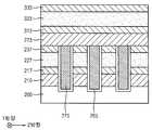
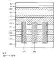
도 30a 및 도 30b는 일 실시예에 따른 적층형 가변 저항 메모리 장치를 나타내는 단면도들이다. 구체적으로, 도 30a 및 도 30b는 각각 제2 방향 및 제1 방향으로의 단면도들이다.30A and 30B are cross-sectional views showing a stacked variable resistance memory device according to an embodiment. Specifically, Figs. 30A and 30B are sectional views in the second direction and the first direction, respectively.
도 30a 및 도 30b는 예시적으로 가변 저항 메모리 장치들이 2층으로 적층된 적층형 가변 저항 메모리 장치를 도시하고 있으며, 도전 라인들의 교차부에 하나의 가변 저항 소자가 배치되는 구조를 도시하고 있다. 상기 적층형 가변 저항 메모리 장치에 포함된 제1 및 제2 가변 저항 메모리 장치들은 도 1 내지 도 3b를 참조하여 설명한 가변 저항 메모리 장치와 실질적으로 동일하거나 유사하다. 이에 따라, 동일한 구성 요소에는 동일한 참조 부호를 부여하고, 이에 대한 자세한 설명은 생략한다.30A and 30B illustrate a stacked variable resistance memory device in which variable resistance memory devices are stacked in two layers and illustrate a structure in which one variable resistance element is disposed at an intersection of conductive lines. The first and second variable resistance memory devices included in the stacked variable resistance memory device are substantially the same as or similar to the variable resistance memory device described with reference to Figs. 1 to 3B. Accordingly, the same components are denoted by the same reference numerals, and a detailed description thereof will be omitted.
도 30a 및 도 30b를 참조하면, 상기 적층형 가변 저항 메모리 장치는 베이스 절연막(200) 상에 형성된 제1 도전 라인(210), 제2 도전 라인(280), 제3 도전 라인(380), 제1 메모리 셀(250), 제2 메모리 셀(350) 및 열 장벽막 패턴 구조물을 포함할 수 있다.30A and 30B, the stacked variable resistance memory device includes a first
예시적인 실시예들에 있어서, 제1 내지 제3 도전 라인들(210, 280, 380)은 각각 복수 개로 형성될 수 있다. 제1 및 제2 도전 라인들(210, 280)이 서로 교차하는 각 교차부에는 제1 메모리 셀(250)이 형성될 수 있으며, 제2 및 제3 도전 라인들(280, 380)이 서로 교차하는 각 교차부에는 제2 메모리 셀(350)이 형성될 수 있다.In exemplary embodiments, each of the first through third
제1 도전 라인(210)은 상기 제1 방향을 따라 연장될 수 있으며, 상기 제2 방향을 따라 복수 개로 형성될 수 있다. 제2 도전 라인(280)은 상기 제2 방향으로 연장될 수 있으며, 상기 제1 방향을 따라 복수 개로 형성될 수 있다. 제3 도전 라인(380)은 제2 도전 라인(280) 상부에 형성되어 상기 제1 방향으로 연장될 수 있으며, 상기 제2 방향을 따라 복수 개로 형성될 수 있다. 이에 따라, 제1 및 제3 도전 라인들(210, 380)은 실질적으로 동일한 방향으로 연장되며, 제2 도전 라인(280)은 제1 및 제3 도전 라인들(210, 380) 사이에 배치되어 이들과 교차하며 연장될 수 있다.The first
예시적인 실시예들에 있어서, 제1 및 제3 도전 라인들(210, 380)은 상기 가변 저항 메모리 장치의 비트 라인 또는 워드 라인으로 제공될 수 있으며, 제2 도전 라인(280)은 제1 및 제3 도전 라인들(210, 380)이 비트 라인으로 제공되는 경우에는 상기 가변 저항 메모리 장치의 공통 워드 라인으로 제공될 수 있으며, 제1 및 제3 도전 라인들(210, 380)이 워드 라인으로 제공되는 경우에는 상기 가변 저항 메모리 장치의 공통 비트 라인으로 제공될 수 있다.In exemplary embodiments, the first and third
제1 내지 제3 도전 라인들(210, 280, 380)이 각각 복수 개로 형성됨에 따라, 제1 및 제2 도전 라인들(210, 280)의 상기 교차부에 형성되는 제1 메모리 셀(250) 및 제2 및 제3 도전 라인들(280, 380)의 상기 교차부에 형성되는 제2 메모리 셀(350) 역시 복수 개로 형성될 수 있다. 이에 따라, 상기 제1 방향을 따라 복수 개로 배치된 제1 및 제2 메모리 셀들(250, 350)은 각각 제1 및 제2 메모리 셀 열(column)들을 정의할 수 있고, 상기 제2 방향을 따라 복수 개로 배치된 제1 및 제2 메모리 셀들(250, 350)은 각각 제1 및 제2 메모리 셀 행(row)을 정의할 수 있다.The
예시적인 실시예들에 있어서, 제1 메모리 셀(250)은 제1 가변 저항층(230)을 포함할 수 있다. 제1 메모리 셀(250)은 제1 가변 저항층(230) 및 제1 도전 라인(210) 사이에 배치되는 제1 하부 전극(220) 및 제1 가변 저항층(230) 및 제2 도전 라인(280) 사이에 배치되는 제1 상부 전극(240)을 더 포함할 수 있다. 이에 따라, 제1 도전 라인(210), 제1 메모리 셀(250) 및 제2 도전 라인(280)를 포함하는 상기 제1 가변 저항 메모리 장치가 형성될 수 있다.In the exemplary embodiments, the
예시적인 실시예들에 있어서, 제2 메모리 셀(350)은 제2 가변 저항층(330)을 포함할 수 있다. 제2 메모리 셀(350)은 제2 가변 저항층(330) 및 제2 도전 라인(280) 사이에 배치되는 제2 하부 전극(320) 및 제2 가변 저항층(330) 및 제3 도전 라인(380) 사이에 배치되는 제2 상부 전극(340)을 더 포함할 수 있다. 이에 따라, 제2 도전 라인(280), 제2 메모리 셀(350) 및 제3 도전 라인(380)을 포함하는 상기 제2 가변 저항 메모리 장치가 형성될 수 있다.In the exemplary embodiments, the
상기 열 장벽막 패턴 구조물은 제1 및 제2 메모리 셀들(250, 350) 사이에 형성될 수 있다. 예시적인 실시예들에 있어서, 상기 열 장벽막 패턴 구조물은 제1 열 장벽막 패턴(275), 제2 열 장벽막 패턴(375a) 및 공통 열 장벽막 패턴(375b)을 포함할 수 있다.The thermal barrier film pattern structure may be formed between the first and
제1 열 장벽막 패턴(275)은 인접하는 상기 제1 메모리 셀 열들 사이에 형성되어, 상기 제1 방향을 따라 연장될 수 있다. 제1 열 장벽막 패턴(275)은 상기 제2 방향으로 인접하는 제1 메모리 셀들(250) 및 제1 도전 라인들(210) 부분을 관통할 수 있다. 예시적인 실시예들에 있어서, 제1 열 장벽막 패턴(275)은 베이스 절연층(200) 내부로도 연장되어 하부가 베이스 절연층(200)에 의해 둘러싸일 수 있다.The first thermal
제2 열 장벽막 패턴(375a)은 인접하는 상기 제2 메모리 셀 열들 사이에 형성되어, 상기 제1 방향을 따라 연장될 수 있다. 제2 열 장벽막 패턴(375a)은 상기 제2 방향으로 인접하는 제2 메모리 셀들(350) 사이를 관통할 수 있다. 예시적인 실시예들에 있어서, 제2 열 장벽막 패턴(375a)은 제2 도전 라인(280)으로도 연장되어 하부가 제2 도전 라인(280)에 의해 둘러싸일 수 있다.The second thermal
공통 열 장벽막 패턴(375b)은 인접하는 상기 제1 및 제2 메모리 셀 행들 사이에 형성되어, 상기 제2 방향을 따라 연장될 수 있다. 공통 열 장벽막 패턴(375b)은 상기 제1 방향으로 인접하는 제2 메모리 셀들(350), 제2 도전 라인들(280) 및 제1 메모리 셀들(250)을 관통할 수 있으며, 제1 도전 라인(210)으로도 연장되어 하부가 제1 도전 라인(210)에 의해 둘러싸일 수 있다.A common thermal
예시적인 실시예들에 있어서, 제1 열 장벽막 패턴(275) 및 공통 열 장벽막 패턴(375b)은 서로 교차하며 연통되며, 제2 열 장벽막 패턴(375a) 및 공통 열 장벽막 패턴(375b) 역시 서로 교차하며 연통될 수 있다. 따라서, 제1 열 장벽막 패턴(275) 및 제2 열 장벽막 패턴(375a)은 공통 열 장벽막 패턴(375b)을 통해 서로 연통될 수 있다.In the exemplary embodiments, the first thermal
제1 및 제2 메모리 셀들(250, 350)의 측벽 상에는 절연막 패턴 구조물이 형성될 수 있다. 예시적인 실시예들에 있어서, 상기 절연막 패턴 구조물은 제1 열 장벽막 패턴(275)을 감싸는 제1 절연막 패턴(265), 제2 열 장벽막 패턴(375a)을 감싸는 제2 절연막 패턴(365a) 및 공통 열 장벽막 패턴(375b)를 감싸는 공통 절연막 패턴(365b)을 포함할 수 있다. 상기 절연막 패턴 구조물은 예를 들어, 실리콘 산화물 또는 실리콘 질화물과 같은 절연 물질을 포함할 수 있다.An insulating film pattern structure may be formed on the sidewalls of the first and
제1 절연막 패턴(265)은 제1 열 장벽막 패턴(275)의 측벽 및 저면을 커버할 수 있으며, 상기 제1 방향을 따라 연장될 수 있다. 제2 절연막 패턴(365a)은 제2 열 장벽막 패턴(375a)의 측벽 및 저면을 커버할 수 있으며, 상기 제1 방향을 따라 연장될 수 있다. 공통 절연막 패턴(365b)은 공통 열 장벽막 패턴(375b)의 측벽 및 저면을 커버할 수 있으며, 상기 제2 방향을 따라 연장될 수 있다.The first
제1 열 장벽막 패턴(275) 및 공통 열 장벽막 패턴(375b)의 일부는 각각 제1 절연막 패턴(265) 및 공통 절연막 패턴(365b)에 의해 인접한 제1 메모리 셀들(250)으로부터 이격될 수 있다. 또한, 제2 열 장벽막 패턴(375a) 및 공통 열 장벽막 패턴(375b)의 일부는 각각 제2 절연막 패턴(365a) 및 공통 절연막 패턴 (365b)에 의해 인접한 제2 메모리 셀들(350)으로부터 이격될 수 있다.Portions of the first thermal
이에 따라, 제1 메모리 셀(250)의 측벽은 제1 절연막 패턴(265) 및 공통 절연막 패턴(365b)에 의해 둘러싸이며, 제1 열 장벽막 패턴(275) 및 공통 열 장벽막 패턴(375b)에 의해 격리된 섬 형상을 가질 수 있다. 또한, 제2 메모리 셀(350)의 측벽은 제2 절연막 패턴(365a) 및 공통 절연막 패턴(365b)에 의해 둘러싸이며, 제2 열 장벽막 패턴(375a) 및 공통 열 장벽막 패턴(375b)에 의해 격리된 섬 형상을 가질 수 있다.The sidewall of the
이때, 각각의 제1 및 제2 열 장벽막 패턴들(273, 375a) 및 공통 열 장벽막 패턴(375b)은 제1 및 제2 메모리 셀들(250, 350)을 둘러싸므로, 이들 사이의 열 전달이 감소될 수 있으며, 이에 따라 상기 가변 저항 메모리 장치의 동작 신뢰성이 향상될 수 있다. 또한, 상기 제2 방향으로 연장되는 공통 절연막 패턴(365b) 및 공통 열 장벽막 패턴(375b)은 상기 제1 가변 저항 메모리 장치 및 상기 제2 가변 저항 메모리 장치에 공통으로 형성되므로, 상기 가변 저항 메모리 장치의 구조 및 제조 공정이 단순화될 수 있다.At this time, since each of the first and second thermal
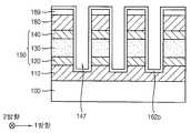
도 31 내지 도 37은 예시적인 실시예들에 따른 적층형 가변 저항 메모리 장치의 제조 방법을 설명하기 위한 단면도들이다. 구체적으로, 도 31, 도 32, 도 33a, 도 36a 및 도 37은 상기 제2 방향으로의 단면도들이고, 도 33b, 도 34, 도 35 및 도 36b는 상기 제1 방향으로의 단면도들이다. 상기 적층형 가변 저항 메모리 장치의 제조 방법은 도 30a 및 도 30b에 도시된 적층형 가변 저항 메모리 장치를 제조하기 위해 사용될 수 있으나, 반드시 이에 한정되는 것은 아니다. 한편, 상기 적층형 가변 저항 메모리 장치의 제조 방법은 도 4 내지 도 13을 참조로 설명한 가변 저항 메모리 장치의 제조 방법에 포함된 공정들과 실질적으로 동일하거나 유사한 공정들을 포함할 수 있으며, 이에 따라 이에 대한 자세한 설명은 생략한다.31 to 37 are sectional views for explaining a method of manufacturing a stacked variable resistance memory device according to exemplary embodiments. Specifically, FIGS. 31, 32, 33A, 36A, and 37 are sectional views in the second direction, and FIGS. 33B, 34, 35, and 36B are sectional views in the first direction. The method of manufacturing the stacked variable resistance memory device can be used for manufacturing the stacked variable resistance memory device shown in FIGS. 30A and 30B, but is not limited thereto. Meanwhile, the manufacturing method of the stacked variable resistance memory device may include processes substantially identical to or similar to those included in the manufacturing method of the variable resistance memory device described with reference to FIGS. 4 to 13, A detailed description will be omitted.
도 31을 참조하면, 도 4를 참조로 설명한 공정과 실질적으로 동일하거나 유사한 공정을 수행한다. 이에 따라, 베이스 절연막(200) 상에 제1 도전막(212), 제1 하부 전극막(213), 제1 가변 저항 물질막(223) 및 제1 상부 전극막(233)을 순차적으로 형성할 수 있다.Referring to FIG. 31, a process substantially the same as or similar to the process described with reference to FIG. 4 is performed. Accordingly, the first
도 32를 참조하면, 도 5a 내지 도 8을 참조로 설명한 공정들과 실질적으로 동일하거나 유사한 공정을 수행한다. 이에 따라, 제1 상부 전극막(233), 제1 가변 저항 물질막(223), 제1 하부 전극막(213) 및 제1 도전막(212)을 관통하며 상기 제1 방향으로 연장하는 제1 트렌치(245)를 형성하고, 제1 트렌치(245)의 측벽 및 저면 상에 제1 절연막 패턴(265)을 형성한 후, 제1 트렌치(245)의 나머지 부분을 채우는 제1 열 장벽막 패턴(275)을 형성할 수 있다. 한편, 제1 트렌치(245)를 형성하기 위한 상기 공정에 의해, 베이스 절연막(200) 상부가 과도 식각될 수 있다.Referring to Fig. 32, a process substantially identical to or similar to the processes described with reference to Figs. 5A to 8 is performed. Accordingly, the first variable
한편, 제1 트렌치(245)가 형성됨에 따라, 제1 도전막(212), 제1 하부 전극막(213), 제1 가변 저항 물질막(223) 및 제1 상부 전극막(233)은 각각 상기 제1 방향을 따라 연장되는 제1 도전 라인(210), 제1 하부 전극막 패턴(217), 제1 가변 저항 물질막 패턴(227) 및 제1 상부 전극막 패턴(237)으로 변환될 수 있다.As the
도 33a 및 도 33b를 참조하면, 도 31을 참조로 설명한 공정과 실질적으로 동일하거나 유사한 공정을 수행함으로써, 제1 상부 전극막 패턴(237), 제1 절연막 패턴(265) 및 제1 열 장벽막 패턴(275) 상에 제2 도전막(273), 제2 하부 전극막(313), 제2 가변 저항 물질막(323) 및 제2 상부 전극막(333)을 순차적으로 형성할 수 있다.Referring to FIGS. 33A and 33B, the first upper
도 34를 참조하면, 제2 상부 전극막(333), 제2 가변 저항 물질막(323), 제2 하부 전극막(313), 제2 도전막(273), 제1 상부 전극막 패턴(237), 제1 가변 저항 물질막 패턴(227) 및 제1 하부 전극막 패턴(217)을 관통하는 공통 트렌치(345)를 형성한다. 예시적인 실시예들에 있어서, 공통 트렌치(345)는 상기 제2 방향을 따라서 연장되며, 상기 제1 방향을 따라 복수 개로 형성될 수 있다.34, a second
예를 들어, 제2 상부 전극막(333) 상에 제2 상부 전극막(333) 상면을 일부 노출시키며 상기 제2 방향으로 연장되는 제2 마스크(339)를 형성할 수 있다. 이후, 제2 마스크(339)를 이용한 건식 식각 공정을 통해 제2 상부 전극막(333), 제2 가변 저항 물질막(323), 제2 하부 전극막(313), 제2 도전막(273), 제1 상부 전극막 패턴(237), 제1 가변 저항 물질막 패턴(227) 및 제1 하부 전극막 패턴(217)을 관통하는 공통 트렌치(345)를 형성할 수 있다. 한편, 공통 트렌치(345) 형성 공정시, 제1 절연막 패턴(265) 및 제1 열 장벽막 패턴(275)의 일부가 함께 제거될 수도 있다.For example, a
예시적인 실시예들에 있어서, 공통 트렌치(345)를 형성하기 위한 상기 식각 공정에 의해 제1 도전 라인(120)의 상부가 과도 식각될 수 있다.In the exemplary embodiments, the top of the first
공통 트렌치(345)가 형성됨에 따라, 제1 하부 전극막 패턴(217), 제1 가변 저항 물질막 패턴(227), 제1 상부 전극막 패턴(237) 및 제2 도전막(273)은 각각 제1 하부 전극(220), 제1 가변 저항층(230), 제1 상부 전극(240) 및 제2 도전 라인(280)으로 변환될 수 있다. 이에 따라, 제1 하부 전극(220), 제1 가변 저항층(230) 및 제1 상부 전극(240)을 포함하는 제1 메모리 셀(250)이 형성될 수 있으며, 제1 도전 라인(210), 제1 메모리 셀(250) 및 제2 도전 라인(280)의 부분을 포함하는 제1 가변 저항 메모리 장치가 형성될 수 있다.The first lower
한편, 공통 트렌치(345)가 형성됨에 따라, 제2 하부 전극막(313), 제2 가변 저항 물질막(323) 및 제2 상부 전극막(333)은 각각 제2 하부 전극막 패턴(317), 제2 가변 저항 물질막 패턴(327) 및 제2 상부 전극막 패턴(337)으로 변환될 수 있다.As the
도 35를 참조하면, 공통 트렌치(345)를 채우며 순차적으로 적층된 공통 절연막 패턴(365b) 및 공통 열 장벽막 패턴(375b)을 형성할 수 있다.Referring to FIG. 35, a common insulating
예시적인 실시예들에 있어서, 도 11 내지 도 13을 참조로 설명한 공정들과 실질적으로 동일하거나 유사한 공정을 수행하여, 공통 트렌치(345)의 측벽 및 저면과 제2 마스크(339) 상에 공통 절연막을 형성하고, 상기 공통 절연막 상에 공통 트렌치(345)의 부분을 채우는 공통 열 장벽막을 형성할 수 있다.In the exemplary embodiments, a process substantially the same or similar to the processes described with reference to FIGS. 11 to 13 may be performed to form a common insulating film on the sidewalls and bottom of the
예시적인 실시예에 있어서, 상기 공통 열 장벽막은 상기 공통 절연막에 포함된 물질보다 열 전도도가 낮은 물질을 포함하도록 형성될 수 있다. 상기 공통 절연막이 실리콘 산화물을 포함하는 경우, 상기 공통 열 장벽막은 실리콘 산화물보다 열 전도도가 낮은 물질을 포함하도록 형성될 수 있다. 일 실시예에 있어서, 상기 공통 열 장벽막은 제1 열 장벽막 패턴(275)과 실질적으로 동일한 물질을 포함하도록 형성할 수 있다.In an exemplary embodiment, the common thermal barrier film may be formed to include a material having a thermal conductivity lower than that of the material contained in the common insulating film. When the common insulating film includes silicon oxide, the common thermal barrier film may be formed to include a material having lower thermal conductivity than silicon oxide. In one embodiment, the common thermal barrier film may be formed to include substantially the same material as the first thermal
이후, 제2 상부 전극막 패턴(337)의 상면이 노출될 때까지, 예를 들어, CMP 공정을 통해 상기 공통 절연막 상부 및 상기 공통 열 장벽막 상부를 평탄화 함으로써 각각 공통 절연막 패턴(365b) 및 공통 열 장벽막 패턴(375b)을 형성할 수 있다. 이때, 제2 마스크(339)는 완전히 제거될 수 있다.Thereafter, the upper portion of the common insulating film and the upper portion of the common thermal barrier film are planarized by, for example, a CMP process until the upper surface of the second upper
예시적인 실시예들에 있어서, 공통 열 장벽막 패턴(375b)은 제1 열 장벽막 패턴(275) 과 서로 교차하며 연결되도록 형성될 수 있다.In the exemplary embodiments, the common thermal
도 36a 및 도 36b를 참조하면, 제2 상부 전극막 패턴(337), 공통 절연막 패턴(365b) 및 공통 열 장벽막 패턴(375b) 상에 제3 도전막(373)을 형성한다. 제3 도전막(373)은 텅스텐, 구리, 알루미늄, 티타늄 또는 탄탈륨과 같은 금속을 사용하여 스퍼터링 공정, ALD 공정, PVD 공정 등을 통해 형성할 수 있다.36A and 36B, a third
도 37을 참조하면, 제3 도전막(373), 제2 상부 전극막 패턴(337), 제2 가변 저항 물질막 패턴(327) 및 제2 하부 전극막 패턴(317)을 관통하는 제2 트렌치(347)를 형성한다. 예시적인 실시예들에 있어서, 제2 트렌치(347)는 상기 제1 방향을 따라서 연장되며, 상기 제2 방향을 따라 복수 개로 형성될 수 있다.Referring to FIG. 37, a second trench 308 is formed through the third
구체적으로, 제3 도전막(373) 상에 제3 도전막(373) 상면을 일부 노출시키며 상기 제1 방향으로 연장되는 제3 마스크(389)를 형성할 수 있다. 이후, 제3 마스크(389)를 이용한 건식 식각 공정을 통해 제3 도전막(373), 제2 상부 전극막 패턴(337), 제2 가변 저항 물질막 패턴(327) 및 제2 하부 전극막 패턴(317)을 관통하는 제2 트렌치(347)를 형성할 수 있다. 한편, 제2 트렌치(347) 형성 공정시, 공통 열 장벽막 패턴(375b) 및 공통 절연막 패턴(365b)의 일부가 함께 제거될 수도 있다.Specifically, a
한편, 제2 트렌치(347)을 형성하기 위한 상기 식각 공정에 의해 제2 도전 라인(280) 상부가 과도 식각될 수 있다.On the other hand, the upper portion of the second
제2 트렌치(347)가 형성됨에 따라, 제2 하부 전극막 패턴(317), 제2 가변 저항 물질막 패턴(327), 제2 상부 전극막 패턴(337) 및 제3 도전막(373)은 각각 상기 제1 방향으로 연장되는 제2 하부 전극(320), 제2 가변 저항층(330), 제2 상부 전극(340) 및 제3 도전 라인(380)으로 변환될 수 있다. 이에 따라, 제2 하부 전극(320), 제2 가변 저항층(330) 및 제2 상부 전극(340)을 포함하는 제2 메모리 셀(350)을 형성할 수 있으며, 제2 도전 라인(280)의 부분, 제2 메모리 셀(350) 및 제3 도전 라인(380)을 포함하는 제2 가변 저항 메모리 장치를 형성할 수 있다.The second lower
다시 도 30a를 참조하면, 도 6 내지 도 8을 참조로 설명한 공정들과 실질적으로 동일하거나 유사한 공정들을 수행하여, 제2 트렌치(347) 내부에 제2 절연막 패턴(365a) 및 제2 열 장벽막 패턴(375a)을 형성할 수 있다.Referring again to FIG. 30A, processes substantially identical to or similar to the processes described with reference to FIGS. 6 to 8 are performed to form a second
구체적으로, 제2 트렌치(347)의 측벽 및 저면 상에 순차적으로 제2 절연막을 형성한 후, GST물질, 다공성 실리콘 산화물 등과 같은 물질을 이용하여 제2 트렌치(347)를 채우는 제2 열 장벽막을 형성할 수 있다. 이후, 제3 도전막(375)의 상면이 노출될 때까지 상기 제2 열 장벽막 및 상기 제2 절연막의 상부를 에치-백 공정을 통해 제거하여, 각각 제2 열 장벽막 패턴(375a) 및 제2 절연막 패턴(365a)을 형성할 수 있다. 이때, 제3 마스크(389)는 제거될 수 있다.Specifically, a second insulating film is sequentially formed on the sidewalls and the bottom of the
예시적인 실시예들에 있어서, 제2 열 장벽막 패턴(375a)은 공통 열 장벽막 패턴(375b)과 서로 교차하며 연결되도록 형성될 수 있다. 공통 열 장벽막 패턴(375b)은 제1 열 장벽막 패턴(275)과 서로 교차하며 연결되므로, 제2 열 장벽막 패턴(375a) 및 제1 열 장벽막 패턴(275)은 공통 열 장벽막 패턴(375b)을 통해 서로 연결될 수 있다.In the exemplary embodiments, the second thermal
예시적인 실시예들에 있어서, 제1 열 장벽막 패턴(275) 및 제2 열 장벽막 패턴(375a)은 상기 제1 방향을 따라 연장되며, 상기 제2 방향을 따라 연장되는 공통 열 장벽막 패턴(375b)과 서로 교차하면서 연통될 수 있다.In the exemplary embodiments, the first thermal
예시적인 실시예들에 있어서, 제1 메모리 셀들(250)은 각각 제1 절연막 패턴(265), 제1 열 장벽막 패턴(275), 공통 절연막 패턴(365b) 및 공통 열 장벽막 패턴(375b)에 의해 측부가 둘러싸일 수 있다. 또한 제2 메모리 셀들(350)은 각각 제2 절연막 패턴(365a), 제2 열 장벽막 패턴(375a), 공통 절연막 패턴(365b) 및 공통 열 장벽막 패턴(375b)에 의해 측부가 둘러싸일 수 있다.In the exemplary embodiments, the
예시적인 실시예들에 따른 상기 적층형 가변 저항 메모리 장치에서, 열 전도도가 낮은 물질을 포함하는 제1 및 제2 열 장벽막 패턴들(275, 375a) 및 공통 열 장벽막 패턴(375b)이 제1 및 제2 메모리 셀들(250, 350)을 둘러싸므로, 이들 사이의 열 전달이 감소될 수 있으며, 이에 따라 동작 신뢰성이 향상될 수 있다.In the stacked variable resistance memory device according to the exemplary embodiments, the first and second thermal
도 28a 내지 도 37에서는 가변 저항 메모리 장치들이 2층으로 적층된 적층형 가변 저항 메모리 장치 및 이의 제조 방법을 도시하였으나, 상기 적층형 가변 저항 메모리 장치는 추가적으로 적층된 가변 저항 메모리 장치들을 더 포함할 수도 있다. 예시적인 실시예들에 있어서, 도 4 내지 도 13, 도 23 내지 27 혹은 도 31 내지 37을 참조로 설명한 공정들을 반복 수행하여 가변 저항 메모리 장치들이 4층으로 적층된 적층형 가변 저항 메모리 장치를 형성할 수도 있다. 이 경우, 가변 저항 메모리 장치들이 2층으로 적층된 적층형 가변 저항 메모리 장치들 사이에 베이스 절연막으로 제공되는 층간 절연막이 형성될 수 있다.28A to 37 illustrate a stacked variable resistance memory device in which variable resistance memory devices are stacked in two layers and a method of manufacturing the same, the stacked variable resistance memory device may further include stacked variable resistance memory devices. In the exemplary embodiments, the processes described with reference to Figs. 4 to 13, 23 to 27, or 31 to 37 are repeated to form a stacked variable resistance memory device in which variable resistance memory devices are stacked in four layers It is possible. In this case, an interlayer insulating film provided as a base insulating film may be formed between the stacked variable resistance memory devices in which the variable resistance memory devices are stacked in two layers.
도 38a 및 도 38b는 예시적인 실시예들에 따른 적층형 가변 저항 메모리 장치를 나타내는 단면도들이다. 구체적으로 도 38a 및 도 38b는 각각 상기 제2 방향 및 제1 방향으로의 단면도들이다.38A and 38B are cross-sectional views illustrating a stacked variable resistance memory device according to exemplary embodiments. Specifically, Figs. 38A and 38B are sectional views in the second direction and the first direction, respectively.
도 38a 및 도 38b는 예시적으로 가변 저항 메모리 장치들이 2층으로 적층된 적층형 가변 저항 메모리 장치를 도시하고 있으며, 도전 라인들의 교차부에 하나의 선택 소자 및 하나의 가변 저항 소자가 배치되는 적층형 가변 저항 메모리 장치를 도시하고 있다. 상기 적층형 가변 저항 메모리 장치는, 제1 선택 소자(S1) 및 제2 선택 소자(S2)를 제외하고는 도 30a 및 도 30b를 참조로 한 적층형 가변 저항 메모리 장치와 실질적으로 동일하거나 유사하다. 이에 따라, 동일한 구성 요소에는 동일한 참조 부호를 부여하고, 이에 대한 자세한 설명은 생략한다.38A and 38B illustrate a stacked variable resistor memory device in which variable resistance memory devices are stacked in two layers by way of example, and a stacked variable memory device in which one selection element and one variable resistance element are disposed at the intersections of the conductive lines A resistive memory device is shown. The stacked variable resistance memory device is substantially the same as or similar to the stacked variable resistance memory device with reference to FIGS. 30A and 30B except for the first selection device S1 and the second selection device S2. Accordingly, the same components are denoted by the same reference numerals, and a detailed description thereof will be omitted.
도 38a 및 도 38b를 참조하면, 상기 적층형 가변 저항 메모리 장치는 베이스 절연막(200) 상에 형성된 제1 가변 저항 메모리 장치, 제2 가변 저항 메모리 장치 및 열 장벽막 패턴 구조물을 포함할 수 있다.38A and 38B, the stacked variable resistance memory device may include a first variable resistance memory device, a second variable resistance memory device, and a thermal barrier film pattern structure formed on the
제1 가변 저항 메모리 장치는 제1 도전 라인(210), 제2 도전 라인(280)의 일부, 제1 메모리셀(250a), 제1 열 장벽막 패턴(275) 및 공통 열 장벽막 패턴(375b)의 일부를 포함할 수 있으며, 제2 가변 저항 메모리 장치는 제2 도전 라인(280)의 일부, 제2 메모리셀(350a). 제3 도전 라인(300), 제2 열 장벽막 패턴(375a) 및 공통 열 장벽막 패턴(375b)의 일부를 포함할 수 있다.The first variable resistance memory device includes a first
제 1 메모리 셀(250a)은 제1 도전 라인(210) 및 제2 도전 라인(280)이 교차하는 교차부에 순차적으로 적층된 제1 선택 소자(S1) 및 제1 가변 저항 소자(R1)를 포함할 수 있으며, 제2 메모리 셀(350a)은 제2 도전 라인(280) 및 제3 도전 라인(380)이 교차하는 교차부에 순차적으로 적층된 제2 가변 저항 소자(R2) 및 제2 선택 소자(S2)를 포함할 수 있다.The
제1 선택 소자(S1) 및 제2 선택 소자(S2)는 P-N 다이오드일 수 있다. 예시적인 실시예들에 있어서, 제1 선택 소자(S1)는 순차적으로 적층된 제1 하부 반도체 층 패턴(205) 및 제1 상부 반도체층 패턴(207)을 포함할 수 있으며, 제2 선택 소자(S2)는 제2 가변 저항 소자(R2) 상에 순차적으로 적층된 제2 상부 반도체층 패턴(355) 및 제2 하부 반도체층 패턴(357)을 포함할 수 있다. 제1 및 제2 하부 반도체층 패턴들(205, 357)은 각각 n형 불순물을 포함하며, 제1 및 제2 상부 반도체층 패턴들(207, 355)은 각각 p형 불순물을 포함할 수 있다. 일 실시예에 있어서, 제1 선택 소자(S1)는 제1 하부 반도체 층 패턴(205) 및 제1 상부 반도체층 패턴(207) 사이에 개재된 제1 절연 패턴(도시되지 않음)을 더 포함할 수 있고, 제2 선택 소자(S2)는 제2 상부 반도체층 패턴(355) 및 제2 하부 반도체층 패턴(357) 사이에 개재된 제2 절연 패턴(도시되지 않음)을 더 포함할 수 있으며, 이 경우 제1 및 제2 선택 소자들(S1, S2)은 각각 P-I-N 다이오드일 수 있다.The first selection device S1 and the second selection device S2 may be P-N diodes. In the exemplary embodiments, the first selection element S1 may include a first lower
제1 가변 저항 소자(R1)는 제1 선택 소자(S1) 상에 순차적으로 적층된 제1 하부 전극(220), 제1 가변 저항층(230) 및 제1 상부 전극(240)을 포함할 수 있으며, 제2 가변 저항 소자(R2)는 순차적으로 적층된 제2 상부 전극(320), 제2 가변 저항층(330) 및 제2 하부 전극(340)을 포함할 수 있다.The first variable resistance element Rl may include a first
상기 열 장벽막 패턴 구조물은 제1 및 제2 메모리 셀들(250, 350) 사이에 형성될 수 있다. 예시적인 실시예들에 있어서, 상기 열 장벽막 패턴 구조물은 제1 열 장벽막 패턴(275), 제2 열 장벽막 패턴(375a) 및 공통 열 장벽막 패턴(375b)을 포함할 수 있다.The thermal barrier film pattern structure may be formed between the first and
제1 열 장벽막 패턴(275)은 상기 제2 방향으로 인접하는 제1 가변 저항 소자들(R1), 제1 선택 소자들(S1) 및 제1 도전 라인들(210) 사이를 관통할 수 있으며, 베이스 절연막(200) 내부로도 연장되어 하부가 베이스 절연막(200)에 의해 둘러싸일 수 있다. 제2 열 장벽막 패턴(375a)은 상기 제2 방향으로 인접하는 제3 도전 라인들(380), 제2 가변 저항 소자들(R2) 및 제2 선택 소자들(S2) 사이를 관통하며, 제2 도전 라인(280) 내부로도 연장되어 하부가 제2 도전 라인(280)에 의해 둘러싸일 수 있다.The first thermal
공통 열 장벽막 패턴(375b)은 제2 메모리 셀(350a) 및 제1 메모리 셀(250a)의 사이를 함께 관통할 수 있으며, 제1 도전 라인(210) 내부로도 연장되어 하부가 제1 도전 라인(210)에 의해 둘러싸일 수 있다. 이에 따라, 공통 열 장벽막 패턴(375b)을 통해 제1 및 제2 열 장벽막 패턴들(275, 375a)이 서로 연통될 수 있다.The common thermal
제1 및 제2 메모리 셀들(250, 350)의 측벽 상에는 절연막 패턴 구조물이 형성될 수 있다. 예시적인 실시예들에 있어서, 상기 절연막 패턴 구조물은 제1 절연막 패턴(265), 제2 절연막 패턴(365a) 및 공통 절연막 패턴(365b)을 포함할 수 있다.An insulating film pattern structure may be formed on the sidewalls of the first and
상기 제1 가변 저항 메모리 장치에 포함되는 제1 메모리 셀들(250a)의 측부는 상기 제1 방향으로 연장되는 제1 절연막 패턴(265) 및 상기 제2 방향으로 연장되는 공통 절연막 패턴(365b)의 일부에 의해 둘러 싸일 수 있다. 제1 절연막 패턴(265) 및 상기 공통 절연막 패턴(365b)은 각각 상기 제1 방향으로 연장되는 제1 열 장벽막 패턴(275) 및 상기 제2 방향으로 연장되는 공통 열 장벽막 패턴(375b)의 일부에 의해 둘러싸일 수 있다. 상기 제2 가변 저항 메모리 장치에 포함되는 제2 메모리 셀들(350a)의 측부는 상기 제1 방향으로 연장되는 제2 절연막 패턴(365a) 및 상기 제2 방향으로 연장되는 공통 절연막 패턴(365b)의 일부에 의해 둘러 싸일 수 있다. 제2 절연막 패턴(365a)은 상기 제2 방향으로 연장되는 제2 열 장벽막 패턴(375a)에 의해 둘러싸일 수 있다.The side of the
도 39 내지 도 44b는 예시적인 실시예들에 따른 적층형 가변 저항 메모리 장치의 제조 방법을 설명하기 위한 단면도들이다. 구체적으로, 도 39, 도 40, 도 41a, 도 43 및 도 44는 상기 제2 방향으로의 단면도들이며, 도 41b 및 도 42는 상기 제1 방향으로의 단면도들이다.FIGS. 39 to 44B are cross-sectional views illustrating a method of manufacturing a stacked variable resistance memory device according to exemplary embodiments. Specifically, Figs. 39, 40, 41A, 43, and 44 are sectional views in the second direction, and Figs. 41B and 42 are sectional views in the first direction.
상기 적층형 가변 저항 메모리 장치의 제조 방법은 도 38a 내지 도 38b에 도시된 적층형 가변 저항 메모리 장치를 제조하기 위해 사용될 수 있으나, 반드시 이에 한정되는 것은 아니다. 한편, 상기 적층형 가변 저항 메모리 장치의 제조 방법은 도 31 내지 도 37을 참조로 설명한 적층형 가변 저항 메모리 장치의 제조 방법에 포함된 공정들과 실질적으로 동일하거나 유사한 공정들을 포함할 수 있으며, 이에 따라 이에 대한 자세한 설명은 생략한다.The method of manufacturing the stacked variable resistance memory device may be used for manufacturing the stacked variable resistance memory device shown in Figs. 38A to 38B, but is not limited thereto. On the other hand, the manufacturing method of the stacked variable resistance memory device may include processes substantially identical to or similar to those included in the manufacturing method of the stacked variable resistance memory device described with reference to FIGS. 31 to 37, A detailed description thereof will be omitted.
도 39를 참조하면, 도 23 및 도 31을 참조로 설명한 공정과 실질적으로 동일하거나 유사한 공정을 수행한다.Referring to Fig. 39, a process substantially identical to or similar to the process described with reference to Figs. 23 and 31 is performed.
이에 따라, 베이스 절연막(200) 상에 제1 도전막(212), 제1 하부 반도체 층(202), 제1 상부 반도체 층(204), 제1 하부 전극막(213), 제1 가변 저항 물질막(223) 및 제1 상부 전극막(233)을 순차적으로 형성한다.Thus, a first
도 40을 참조하면, 도 24 및 25 또는 도 34 및 도 35를 참조로 설명한 공정과 실질적으로 동일하거나 유사한 공정을 수행한다.Referring to Fig. 40, a process substantially identical to or similar to the process described with reference to Figs. 24 and 25 or Figs. 34 and 35 is performed.
이에 따라, 제1 상부 전극막(233), 제1 가변 저항 물질막(223), 제1 하부 전극막(213), 제1 상부 반도체 층(204), 제1 하부 반도체 층(202) 및 제1 도전막(212)을 관통하는 제1 트렌치(245)를 형성하고, 제1 트렌치(245) 내부에 상기 제1 방향을 따라 연장되는 제1 절연막 패턴(265) 및 제1 열 장벽막 패턴(275)을 형성할 수 있다.Accordingly, the first
한편, 제1 트렌치(245)가 형성됨에 따라, 제1 상부 전극막(233), 제1 가변 저항 물질막(223), 제1 하부 전극막(213), 제1 상부 반도체 층(204), 제1 하부 반도체 층(202) 및 제1 도전막(212)은 각각 제1 상부 전극막 패턴(237), 제1 가변 저항 물질막 패턴(227), 제1 하부 전극막 패턴(217), 제1 상부 반도체층 라인(208), 제1 하부 반도체층 라인(206) 및 제1 도전 라인(210)으로 변환될 수 있다.As the
도 41a 및 도 41b를 참조하면, 도 33a 및 도 33b를 참조로 설명한 공정과 실질적으로 동일하거나 유사한 공정을 수행한다.Referring to Figs. 41A and 41B, a process substantially identical to or similar to the process described with reference to Figs. 33A and 33B is performed.
이에 따라, 제1 상부 전극막 패턴(237), 제1 절연막 패턴(265) 및 제1 열 장벽막 패턴(275) 상에 제2 도전막(273), 제2 상부 전극막(313), 제2 가변 저항 물질막(323), 제2 하부 전극막(333), 제2 상부 반도체층(352) 및 제2 하부 반도체층(354)을 순차적으로 형성할 수 있다.The second
도 42를 참조하면, 도 34 및 도 35를 참조로 설명한 공정들과 실질적으로 동일하거나 유사한 공정들을 수행한다.Referring to Fig. 42, processes substantially identical to or similar to the processes described with reference to Figs. 34 and 35 are performed.
이에 따라, 상기 제2 방향을 따라 연장되며, 제2 하부 반도체층(354), 제2 상부 반도체층(352), 제2 하부 전극막(333), 제2 가변 저항 물질막(323), 제2 상부 전극막(313), 제2 도전막(273), 제1 상부 전극막 패턴(237), 제1 가변 저항 물질막 패턴(227), 제1 하부 전극막 패턴(217), 제1 상부 반도체층 라인(208), 제1 하부 반도체층 라인(206) 및 제1 도전 라인(210) 상부를 상기 제1 방향으로 관통하는 공통 트렌치(345)를 형성한 후, 공통 트렌치(345) 내부에 공통 절연막 패턴(365b) 및 공통 열 장벽막 패턴(375b)을 형성할 수 있다.Accordingly, the second
공통 트렌치(345)가 형성됨에 따라, 제2 하부 반도체층(354), 제2 상 반도체층(352)은 각각 제2 하부 반도체층 라인(358), 제2 상부 반도체층 라인(356)으로 변환될 수 있다. 또한, 제2 하부 전극막(333), 제2 가변 저항 물질막(323), 제2 상부 전극막(313) 및 제2 도전막(273)은 각각 제2 하부 전극막 패턴(337), 제2 가변 저항 물질막 패턴(327), 제2 상부 전극막 패턴(317) 및 제2 도전 라인(280)으로 변환될 수 있다.The second
한편, 제1 상부 전극막 패턴(237), 제1 가변 저항 물질층 패턴(227), 제1 하부 전극막 패턴(217), 제1 상부 반도체층 라인(208) 및 제1 하부 반도체층 라인(206)은 각각 제1 상부 전극(240), 제1 가변 저항층(230), 제1 하부 전극(220), 제1 상부 반도체층 패턴(207) 및 제1 하부 반도체층 패턴(205)으로 변환될 수 있다. 이에 따라, 제1 하부 반도체층 패턴(205) 및 제1 상부 반도체층 패턴(207)을 포함하는 제1 선택 소자(S1)가 형성될 수 있으며, 제1 하부 전극(220), 제1 가변 저항층(230) 및 제1 상부 전극(240)을 포함하는 제1 가변 저항 소자(R1)가 형성될 수 있다. 제1 도전 라인(210) 및 제2 도전 라인(280)의 교차부에는 제1 선택 소자(S1) 및 제1 가변 저항 소자(R1)를 포함하는 제1 메모리 셀(250a)이 형성될 수 있다.The first upper
도 43을 참조하면, 도 36a 및 도 37을 참조로 설명한 공정들과 실질적으로 동일하거나 유사한 공정들을 수행한다.Referring to FIG. 43, substantially similar processes as those described with reference to FIGS. 36A and 37 are performed.
이에 따라, 제2 하부 반도체층 라인(358), 공통 절연막 패턴(365b) 및 공통 열 장벽막 패턴(375b) 상에 제3 도전막을 형성하고, 상기 제3 도전막, 제2 하부 반도체층 라인(358), 제2 상부 반도체층 라인(356), 제2 하부 전극막 패턴(337), 제2 가변 저항 물질막 패턴(327), 제2 상부 전극막 패턴(317) 및 제2 도전 라인(280)을 관통하며 상기 제1 방향으로 연장되는 제2 트렌치(347)를 형성할 수 있다. 한편, 제2 트렌치(347)을 형성하기 위한 공정에서, 제2 도전 라인(280)이 과식각 될 수 있다. 이후, 제2 트렌치(347)의 측벽 및 저면 상에 제2 절연막 패턴(365a) 및 제2 트렌치(347)를 채우는 제2 열 장벽막 패턴(375a)을 형성할 수 있다.Thus, a third conductive film is formed on the second lower
제2 트렌치(347)가 형성됨에 따라, 상기 제3 도전막, 제2 하부 전극막 패턴(337), 제2 가변 저항 물질막 패턴(327) 및 제2 상부 전극막 패턴(320)은 각각 제3 도전 라인(380), 제2 하부 전극(370), 제2 가변 저항층(330) 및 제2 상부 전극(320)으로 변환될 수 있다. 이에 따라, 순차적으로 적층된 제2 상부 전극(320), 제2 가변 저항층(330) 및 제2 하부 전극(370)을 포함하는 제2 가변 저항 소자(R2)를 형성할 수 있다.As the
또한, 제2 하부 반도체층 라인(358) 및 제2 상부 반도체층 라인(356)은 각각 제2 하부 반도체층 패턴(357) 및 제2 상부 반도체층 패턴(355)으로 변환될 수 있다. 이에 따라, 순차적으로 적층된 제2 상부 반도체층 패턴(355) 및 제2 하부 반도체층 패턴(357)을 포함하는 제2 선택 소자(S2)를 형성할 수 있다.The second lower
이에 의해, 제2 도전 라인(280) 및 제3 도전 라인(380)의 교차부에는 순차적으로 적층된 제2 가변 저항 소자(R2) 및 제2 선택 소자(S2)를 포함하는 제2 메모리 셀(350a)을 형성할 수 있다.A second memory cell including a second variable
일 실시예에 있어서, 도 39 내지 도 43을 참조로 설명한 공정들을 반복하여 상기 가변 저항 메모리 장치들이 4층 이상으로 적층된 적층형 가변 저항 메모리 장치를 형성할 수도 있다.In one embodiment, the processes described with reference to FIGS. 39 to 43 may be repeated to form a stacked variable resistance memory device in which the variable resistance memory devices are stacked in four or more layers.
도 44는 예시적인 실시예들에 따른 반도체 장치를 나타내는 단면도이다. 도 44는 트랜지스터 및 배선을 포함하는 하부 구조물 상에 예시적인 실시예들에 따른 가변 저항 메모리 장치가 적층된 반도체 장치를 예시적으로 도시하고 있다.44 is a cross-sectional view showing a semiconductor device according to exemplary embodiments. Figure 44 illustrates, by way of example, a semiconductor device in which a variable resistance memory device according to exemplary embodiments is stacked on a substructure including transistors and wires.
도 44를 참조하면, 상기 하부 구조물은 기판(400) 상에 형성된 게이트 구조물(430), 제1 내지 제3 층간 절연막들(440, 460, 480), 제1 내지 제3 콘택들(445, 465, 485) 및 제1 및 제2 배선들(450, 470)을 포함할 수 있다.44, the lower structure includes a
기판(400)은 단결정 실리콘 또는 단결정 게르마늄을 포함하는 반도체 기판 일 수 있다. 기판(400) 상부에는 소자 분리막(402)이 형성되어 기판(400)의 액티브 영역 및 필드 영역이 정의될 수 있다.The
게이트 구조물(430)은 기판(400) 상에 순차적으로 적층되는 게이트 절연막 패턴(410), 게이트 전극(415) 및 게이트 마스크(420)를 포함할 수 있다.The
게이트 절연막 패턴(410)은 실리콘 산화물 또는 금속 산화물을 포함할 수 있고, 게이트 전극(415)은 불순물이 도핑된 폴리실리콘, 금속 혹은 금속 질화물을 포함할 수 있으며, 게이트 마스크(420)는 실리콘 질화물을 포함할 수 있다. 게이트 구조물(430)의 측벽 상에는 게이트 스페이서(435)가 형성될 수 있다.The gate insulating
게이트 구조물(430)과 인접한 기판(400) 상부에는 불순물 영역(405)이 형성될 수 있다. 예를 들어, 불순물 영역(405)은 인(P) 또는 비소(As)와 같은 n형 불순물을 포함할 수 있다. 이 경우, 게이트 구조물(430) 및 불순물 영역(405)을 포함하는 엔모스(Negative Metal Oxide Semiconductor: NMOS) 트랜지스터가 형성될 수 있으며, 도 47에 도시된 기판(400) 부분은 NMOS 영역일 수 있다.An
일 실시예에 있어서, 기판(400)은 피모스(Positive Metal Oxide Semiconductor: PMOS) 영역을 더 포함할 수 있으며, 상기 PMOS 영역의 기판(400) 상에는 p형 불순물 영역 및 게이트 구조물을 포함하는 PMOS 트랜지스터(도시되지 않음)가 더 형성될 수도 있다. 이 경우, 상기 기판(400) 상에는 상보형(Complementary Metal Oxide Semiconductor Transistor: CMOS) 트랜지스터가 형성될 수 있다.In one embodiment, the
일 실시예에 있어서, 게이트 구조물(430)은 기판(400) 내부로 적어도 일부가 매립된 매립 게이트 구조를 가질 수도 있다. 이 경우, 기판(400)을 일부 식각하여 리세스(도시되지 않음)를 형성한 후, 상기 리세스 내부에 게이트 절연막 패턴 및 게이트 전극을 형성할 수 있다.In one embodiment, the
기판(400) 상에는 게이트 구조물(430), 게이트 스페이서(435) 및 불순물 영역(405)을 커버하는 제1 층간 절연막(440)이 형성되고, 제1 층간 절연막(440)을 관통하여 불순물 영역(405)과 접촉하는 제1 콘택(445)이 형성될 수 있다. 제1 층간 절연막(440) 상에는 제1 배선(450)이 형성되어, 제1 콘택(445)과 전기적으로 연결될 수 있다.A first
제1 층간 절연막(440) 상에는 제1 배선(450)을 덮는 제2 층간 절연막(460)이 형성되고, 제2 층간 절연막(460)을 관통하여 제1 배선(450)과 접속되는 제2 콘택(465)이 형성될 수 있다. 제2 층간 절연막(460) 상에는 제2 배선(470)이 형성되어, 제2 콘택(465)과 전기적으로 연결될 수 있다. 일 실시예에 있어서, 제2 배선(470)의 부분은 상기 PMOS 영역까지 연장되어 상기 PMOS 트랜지스터의 불순물 영역과 전기적으로 연결될 수 있다.A second
제2 층간 절연막(460) 상에는 제2 배선(470)을 덮는 제3 층간 절연막(480)이 형성되고, 제3 층간 절연막(480)을 관통하여 제2 배선(470)과 접속되는 제3 콘택(485)이 형성될 수 있다.A third
제1 내지 제3 층간 절연막들(440, 460, 480)은 실리콘 산화물을 포함하며, 실질적으로 상술한 베이스 절연막으로 제공될 수 있다. 제1 내지 제3 콘택들(445, 465, 485), 제1 배선(450) 및 제2 배선(470)은 텅스텐, 알루미늄, 구리, 티타늄 등과 같은 금속 및/또는 이들 금속의 질화물을 포함할 수 있다.The first to third
제3 층간 절연막(480) 상에는 예시적인 실시예들에 따른 가변 저항 메모리 장치가 형성될 수 있다. 예를 들어, 도 38a 및 38b를 참조로 설명한 가변 저항 메모리 장치의 제1 도전 라인(210)은 제3 콘택(485)과 전기적으로 연결될 수 있다.On the third
상기 가변 저항 메모리 장치는 도전 라인들이 교차되는 교차부에 형성되며 하나의 선택 소자 및 하나의 가변 저항 소자를 포함하는 가변 저항 메모리 장치일 수 있다. 예를 들어, 상기 가변 저항 메모리 장치는 도 22a 및 도 22b, 도 29a 및 도 29b, 또는 도 38a 및 38b를 참조로 설명한 상기 가변 저항 메모리 장치들과 실질적으로 동일하거나 유사할 수 있다.The variable resistance memory device may be a variable resistance memory device formed at an intersection at which the conductive lines are crossed and including one selection element and one variable resistance element. For example, the variable resistive memory device may be substantially the same or similar to the variable resistive memory devices described with reference to Figures 22A and 22B, 29A and 29B, or 38A and 38B.
다른 예시적인 실시예들에 있어서, 상기 가변 저항 메모리 장치는 도 28a 및 도 28b에 도시된 바와 같이, 상기 도전 라인들이 교차되는 상기 교차부에 형성되며 하나의 상기 가변 저항 소자를 포함하는 가변 저항 메모리 장치일 수 있다. 또한, 상기 가변 저항 메모리 장치는 도 1 내지 도 3b, 도 14 내지 15b, 및 도 30a 및 도 30b를 참조로 설명한 가변 저항 메모리 장치들과 실질적으로 동일하거나 유사할 수 있다.28A and 28B, the variable resistance memory device includes a variable resistance memory (not shown) formed at the intersection at which the conductive lines are crossed and includes one variable resistance element, Device. Further, the variable resistance memory device may be substantially the same as or similar to the variable resistance memory devices described with reference to Figs. 1 to 3B, 14 to 15B, and 30A and 30B.
상기 가변 저항 메모리 장치는 상기 도면들을 참조로 설명한 가변 저항 메모리 장치들과 실질적으로 동일하거나 유사하므로 추가적인 상세한 설명은 생략한다.The variable resistance memory device is substantially the same as or similar to the variable resistance memory devices described with reference to the drawings, so that detailed description is omitted.
한편, 도 44에서는 상기 배선들이 2층으로 적층된 상기 하부 구조물을 도시하였으나, 이에 한정되는 것은 아니다. 예를 들어, 상기 하부 구조물은 단층의 배선 혹은 3층 이상으로 적층된 배선들을 포함할 수도 있다.On the other hand, in FIG. 44, the lower structure in which the wirings are stacked in two layers is shown, but the present invention is not limited thereto. For example, the substructure may include single layer wiring or three or more layers of stacked wiring.
도 45 내지 도 48은 예시적인 실시예들에 따른 반도체 장치의 제조 방법을 설명하기 위한 단면도들이다. 상기 가변 저항 메모리 장치의 제조 방법은 도 44에 도시된 가변 저항 메모리 장치를 제조하기 위해 사용될 수 있으나, 반드시 이에 한정되는 것은 아니다.45 to 48 are sectional views for explaining a method of manufacturing a semiconductor device according to exemplary embodiments. The manufacturing method of the variable resistance memory device can be used for manufacturing the variable resistance memory device shown in FIG. 44, but it is not limited thereto.
도 45를 참조하면, 기판(400) 상에 게이트 구조물(430)을 형성한 후, 게이트 구조물(430)과 인접한 기판(400) 상부에 불순물 영역(405)을 형성한다.Referring to FIG. 45, a
기판(400)은 NMOS 영역 및 PMOS 영역을 포함할 수 있으며, 기판(400) 상에는 CMOS 트랜지스터가 형성될 수 있다. 한편, 얕은 트렌치 분리(Shallow Trench Isolation) 공정을 통해 기판(400) 상부에 소자 분리막(402)을 형성할 수 있다. 소자 분리막(402)에 의해 기판(400)의 액티브 영역 및 필드 영역이 구분될 수 있다.The
예시적인 실시예들에 있어서, 기판(400) 상에 게이트 절연막, 게이트 전극막 및 게이트 마스크막을 순차적으로 형성한 후, 사진 식각 공정을 통해 이들을 식각하여 게이트 절연막 패턴(410), 게이트 전극(415) 및 게이트 마스크(420)를 포함하는 게이트 구조물(430)을 형성할 수 있다.In the exemplary embodiments, a gate insulating film, a gate electrode film, and a gate mask film are sequentially formed on the
상기 게이트 절연막은 예를 들어, 실리콘 산화물을 사용하여 CVD 공정 또는 열 산화 공정을 통해 형성될 수 있다. 상기 게이트 전극막은 도핑된 폴리실리콘, 금속 혹은 금속 질화물을 사용하여 스퍼터링 공정 또는 ALD 공정을 통해 형성될 수 있다. 상기 게이트 마스크막은 예를 들어 실리콘 질화물을 사용하여 CVD 공정, 스핀 코팅 공정 등을 통해 형성될 수 있다.The gate insulating film may be formed through a CVD process or a thermal oxidation process using, for example, silicon oxide. The gate electrode film may be formed by a sputtering process or an ALD process using doped polysilicon, metal, or metal nitride. The gate mask film can be formed through a CVD process, a spin coating process, or the like using, for example, silicon nitride.
이후, 게이트 구조물(430)을 이온 주입 마스크로 사용하여 기판(400) 상부에 불순물을 주입함으로써 불순물 영역(405)을 형성할 수 있다. 예시적인 실시예들에 있어서, 불순물 영역(405)은 인, 비소와 같은 n형 불순물을 포함할 수 있다. 이때, 도 48에 도시된 기판(400) 부분은 NMOS 영역으로 제공될 수 있으며, 이에 따라, 불순물 영역(405) 및 게이트 구조물(430)을 포함하는 NMOS 트랜지스터를 형성할 수 있다. 기판(400)의 PMOS 영역 상에는 상기 NMOS 트랜지스터와 동시에 PMOS 트랜지스터(도시되지 않음)가 형성될 수도 있다.Then, the
일 실시예에 있어서, 게이트 구조물(430)의 측벽 상에 게이트 스페이서(435)를 더 형성할 수 있다. 예를 들어, 기판(400) 상에 게이트 구조물(430)을 커버하는 스페이서막을 형성한 후, 상기 스페이서막을 이방성 식각하여 게이트 스페이서(435)를 형성할 수 있다. 상기 스페이서막은 실리콘 질화물을 사용하여, CVD 공정을 통해 형성될 수 있다.In one embodiment,
도 46를 참조하면, 기판(400) 상에 게이트 구조물(430)을 커버하는 제1 층간 절연막(440)을 형성한다. 이후, 제1 층간 절연막(440)을 관통하여 불순물 영역(405)과 접속하는 제1 콘택(445)을 형성한다.Referring to FIG. 46, a first
예를 들어, 제1 층간 절연막(440)은 TEOS와 같은 실리콘 산화물을 사용하여 CVD 공정, 스핀 코팅 공정 등을 통해 형성될 수 있다. 이후, 층간 절연막(440)을 부분적으로 식각하여, 불순물 영역(405)을 노출시키는 제1 콘택 홀을 형성할 수 있다. 층간 절연막(440) 상에 상기 제1 콘택 홀을 채우는 제1 도전막을 형성한 후, 층간 절연막(440) 상면이 노출될 때까지 상기 제1 도전막 상부를 평탄화하여 제1 콘택(445)을 형성할 수 있다.For example, the first
일 실시예에 있어서, 제1 콘택(445)은 게이트 스페이서(435)에 자기 정렬되도록 형성되어, 게이트 스페이서(435)의 측벽과 접촉할 수 있다.In one embodiment, the
제1 층간 절연막(440) 상에는 제1 콘택(445)과 전기적으로 연결되는 제1 배선(450)을 형성할 수 있다. 예를 들어, 제1 층간 절연막(440) 및 제1 콘택(445) 상에 제2 도전막을 형성한 후, 상기 제2 도전막을 패터닝하여 제1 배선(450)을 형성할 수 있다. 상기 제1 및 제2 도전막들은 금속 혹은 금속 질화물을 사용하여 ALD 공정, 스퍼터링 공정 등을 통해 형성될 수 있다.A
도 47을 참조하면, 제1 층간 절연막(440) 상에 제1 배선(450)을 덮는 제2 층간 절연막(460)을 형성할 수 있다. 이후, 제2 층간 절연막(460)을 관통하며 제1 배선(450)을 적어도 부분적으로 노출시키는 제2 콘택 홀을 형성할 수 있다. 제2 층간 절연막(460) 상에 상기 제2 콘택 홀을 채우는 제3 도전막을 형성하고, 상기 제3 도전막의 상부를 CMP 공정을 통해 평탄화함으로써 제1 배선(450)과 전기적으로 연결되는 제2 콘택(465)을 형성할 수 있다.Referring to FIG. 47, a second
제2 층간 절연막(460) 및 제2 콘택(465) 상에 제4 도전막을 형성한 후, 상기 제4 도전막을 패터닝하여 제2 콘택(465)과 전기적으로 연결되는 제2 배선(470)을 형성할 수 있다. 예시적인 실시예들에 있어서, 제2 배선들(470)이 복수 개로 형성되며, 제2 배선들(470)의 부분은 상기 PMOS 영역으로 연장되어, p형 불순물 영역을 포함하는 상기 PMOS 트랜지스터와 전기적으로 연결될 수 있다.A fourth conductive film is formed on the second
제2 층간 절연막(460) 상에 제2 배선(470)을 덮는 제3 층간 절연막(480)을 형성할 수 있다. 이후, 제3 층간 절연막(480)을 관통하여 제2 배선(470)을 노출시키는 제3 콘택 홀을 형성할 수 있다. 제3 층간 절연막(480) 상에 상기 제3 콘택 홀을 채우는 제5 도전막을 형성한 후, 상기 제5 도전막 상부를 평탄화하여 제2 배선(470)과 전기적으로 연결되는 제3 콘택(485)을 형성할 수 있다.A third
제2 및 제3 층간 절연막들(460, 480)은 제1 층간 절연막(440)과 실질적으로 동일하거나 유사한 실리콘 산화물을 사용하여 CVD 공정, 스핀 코팅 공정 등을 통해 형성될 수 있다. 제3 내지 제5 도전막들은 텅스텐, 알루미늄, 구리, 티타늄 등과 같은 금속 및/또는 이들 금속의 질화물을 사용하여 ALD 공정, 스퍼터링 공정, PVD 공정 등을 통해 형성될 수 있다.The second and third
이에 따라, 상기 공정에 의해 기판(400), 트랜지스터, 배선 구조물을 포함하는 하부 구조물이 형성될 수 있다. 상기 하부 구조물은 2층으로 적층된 배선들을 포함하는 것으로 설명하였으나, 반드시 이에 한정되는 것은 아니다.Accordingly, the lower structure including the
도 48을 참조하면, 상기 하부 구조물 상에 가변 저항 메모리 장치를 형성한다. 예를 들어, 도 39 내지 도 43을 참조로 설명한 공정들과 실질적으로 동일하거나 유사한 공정들을 수행하여, 도 38a 및 도 38b를 참조로 설명한 가변 저항 메모리 장치를 상기 하부 구조물 상에 형성할 수 있다. 이때, 상기 가변 저항 메모리 장치의 제1 도전 라인(210)은 상기 하부 구조물의 제3 콘택(485)과 전기적으로 연결될 수 있다.Referring to Figure 48, a variable resistance memory device is formed on the substructure. For example, substantially the same or similar processes as those described with reference to Figs. 39 to 43 may be performed to form the variable resistance memory device described above with reference to Figs. 38A and 38B on the substructure. At this time, the first
다른 예시적인 실시예들에 있어서, 도 4 내지 도 13, 도 16 내지 도21, 도 23 내지 도 27, 도 31 내지 도 37, 또는 도 39 내지 도 43을 참조로 설명한 공정들과 실질적으로 동일하거나 유사한 공정들을 통해 각각 도 1 내지 도 3b, 도 14 내지 도 15b, 도 22 및 도 22b, 도 30a 및 30b, 또는 도 38a 및 38b에 도시된 가변 저항 메모리 장치를 상기 하부 구조물 상에 형성할 수도 있다. 또한, 도 28a 및 도 29b 또는 도 29a 및 도 29b를 참조로 설명한 가변 저항 메모리 장치를 상기 하부 구조물 상에 형성할 수도 있다.In other exemplary embodiments, substantially the same as the processes described with reference to Figs. 4 to 13, 16 to 21, 23 to 27, 31 to 37, or 39 to 43 Variable resistive memory devices shown in Figures 1 to 3B, 14 to 15B, 22 and 22B, 30A and 30B, or 38A and 38B, respectively, may be formed on the substructure through similar processes . The variable resistance memory device described with reference to Figs. 28A and 29B or Figs. 29A and 29B may also be formed on the substructure.
도 49는 예시적인 실시예들에 따른 정보처리 시스템의 개략적인 구성을 나타내는 블록도이다.49 is a block diagram showing a schematic configuration of an information processing system according to exemplary embodiments;
도 49를 참조하면, 정보처리 시스템(500)은 시스템 버스(505)에 전기적으로 연결된 중앙처리장치(CPU)(520), 램(RAM)(530), 사용자 인터페이스(User Interface)(540), 베이스밴드 칩셋(Baseband chipset)과 같은 모뎀(MODEM)(550) 및 메모리 시스템(510)을 포함할 수 있다. 메모리 시스템(510)은 메모리 소자(512)와 메모리 컨트롤러(511)를 포함할 수 있다. 메모리 소자(512)는 상술한 예시적인 실시예들에 따른 가변 저항 메모리 장치를 포함할 수 있다. 따라서, 중앙처리장치(520)에서 처리된 데이터 또는 외부에서 입력된 고용량의 데이터를 안정적으로 저장할 수 있다. 메모리 컨트롤러(511)는 메모리 소자(512)를 제어할 수 있도록 구성된다. 메모리 소자(512)와 메모리 컨트롤러(511)의 결합에 의해 메모리 시스템(510)은 메모리 카드 또는 반도체 디스크 장치(Solid State Disk: SSD) 등으로 제공될 수 있다. 정보처리 시스템(500)이 모바일 장치인 경우, 정보처리 시스템(500)의 동작 전압을 공급하기 위한 배터리가 추가적으로 제공될 수 있다. 도시되지 않았지만, 예시적인 실시예들에 따른 정보처리 시스템(500)에는 응용 칩셋(Application chipset), 카메라 이미지 프로세서(Camera Image Processor: CIS), 모바일 디램 등이 더 포함될 수도 있다. 이러한, 정보처리 시스템(500)은 모바일 폰, MP3 플레이어, 각종 가전 제품 등에 이용될 수 있다.49, the
본 발명의 예시적인 실시예들에 있어서, 가변 저항 메모리 장치는 인접하는 메모리 셀들을 둘러싸는 절연막 패턴들 상에 형성된 열 장벽막 패턴을 포함한다. 상기 열 장벽막 패턴들은 열 전도도가 낮은 물질을 포함하므로, 상기 메모리 셀들 사이의 열 전달을 감소시켜, 상기 가변 저항 메모리 장치의 동작 신뢰성이 향상될 수 있다. 따라서, 예시적인 실시예들에 따른 가변 저항 메모리 장치는 높은 신뢰성이 요구되는 ReRAM, PRAM, MRAM 장치 등에 효과적으로 적용될 수 있다.In exemplary embodiments of the present invention, the variable resistance memory device includes a thermal barrier film pattern formed on insulating film patterns surrounding adjacent memory cells. The thermal barrier film patterns include a material having a low thermal conductivity, so that heat transfer between the memory cells is reduced, so that operational reliability of the variable resistive memory device can be improved. Therefore, the variable resistance memory device according to the exemplary embodiments can be effectively applied to ReRAM, PRAM, MRAM devices and the like which require high reliability.
상술한 바와 같이 본 발명의 바람직한 실시예들을 참조하여 설명하였지만 해당 기술 분야에서 통상의 지식을 가진 자라면 특허 청구 범위에 기재된 본 발명의 사상 및 영역으로부터 벗어나지 않는 범위 내에서 본 발명을 다양하게 수정 및 변경시킬 수 있음을 이해할 수 있을 것이다.It will be apparent to those skilled in the art that various modifications and variations can be made in the present invention without departing from the spirit or scope of the invention as defined in the appended claims. It will be understood that the present invention can be changed.
S: 선택 소자R: 가변 저항 소자
100, 200: 베이스 절연막102: 하부 반도체층
104: 상부 반도체층105: 하부 반도체층 패턴
106: 하부 반도체층 라인107: 상부 반도체층 패턴
108: 상부 반도체층 라인110, 210: 제1 도전 라인
112, 212: 제1 도전막113: 하부 전극막
117: 하부 전극막 패턴120: 하부 전극
123: 가변 저항 물질막127: 가변 저항 물질막 패턴
130: 가변 저항층133: 상부 전극막
137: 상부 전극막 패턴139: 제1 마스크
140: 상부 전극145, 245: 제1 트렌치
147, 347: 제2 트렌치145b: 제1 개구
147b: 제2 개구 150, 150a: 메모리 셀
160: 교차부
160a: 제1 절연막 162b: 제2 절연막
165a, 265: 제1 절연막 패턴165b, 365a: 제2 절연막 패턴
167a: 제3 절연막 패턴 167b: 제4 절연막 패턴
175a, 275: 제1 열 장벽막 패턴 175b, 375a: 제2 열 장벽막 패턴
177: 제2 도전막180, 280: 제2 도전 라인
182: 제1 리세스 184: 제2 리세스
189, 339: 제2 마스크
202: 제1 하부 반도체층204: 제1 상부 반도체층
206: 제1 하부 반도체층 라인 205: 제1 하부 반도체층 패턴
207: 제1 상부 반도체층 패턴 208: 제1 상부 반도체층 라인
213: 제1 하부 전극막220: 제1 하부 전극
217: 제1 하부 전극막 패턴223: 제1 가변 저항 물질막
227: 제1 가변 저항 물질막 패턴 230: 제1 가변 저항층
233: 제1 상부 전극막240: 제1 상부 전극
237: 제1 상부 전극막 패턴250, 250a: 제1 메모리 셀
273: 제2 도전막280: 제2 도전 라인
313: 제2 상부 전극막 317: 제2 상부 전극막 패턴
320: 제2 상부 전극 323: 제2 가변 저항 물질막
327: 제2 가변 저항 물질막 패턴 330: 제2 가변 저항층
333: 제2 하부 전극막 337: 제2 하부 전극막 패턴
340: 제2 하부 전극 345: 공통 트렌치
350, 350a: 제2 메모리 셀
352: 제2 상부 반도체층354: 제2 하부 반도체층
355: 제2 상부 반도체층 패턴 356: 제2 상부 반도체층 라인
357: 제2 하부 반도체층 패턴 358: 제2 하부 반도체층 라인
365b: 공통 절연막 패턴
375b: 공통 열 장벽막 패턴 373: 제3 도전막
380: 제3 도전 라인389: 제3 마스크
400: 기판 402: 소자 분리막
405: 불순물 영역 410: 게이트 절연막 패턴
415: 게이트 전극420: 게이트 마스크
430: 게이트 구조물 435: 게이트 스페이서
440: 제1 층간 절연막 445: 제1 콘택
450: 제1 배선 460: 제2 층간 절연막
465: 제2 콘택 470: 제2 배선
480: 제3 층간 절연막 485: 제3 콘택
500: 정보처리 시스템 505: 시스템 버스
510: 메모리 시스템 511: 메모리 컨트롤러
512: 메모리 소자 520: 중앙처리장치
530: 램 540: 사용자 인터페이스
550: 모뎀S: Selection element R: Variable resistance element
100, 200: base insulating film 102: lower semiconductor layer
104: upper semiconductor layer 105: lower semiconductor layer
106: lower semiconductor layer line 107: upper semiconductor layer pattern
108: upper
112, 212: first conductive film 113: lower electrode film
117: lower electrode film pattern 120: lower electrode
123: Variable resistance material film 127: Variable resistance material film pattern
130: variable resistance layer 133: upper electrode film
137: upper electrode film pattern 139: first mask
140:
147, 347:
147b:
160: intersection
160a: first insulating
165a, 265: First insulating
167a: third insulating
175a, 275: First thermal
177: second
182: first recess 184: second recess
189, 339: Second mask
202: first lower semiconductor layer 204: first upper semiconductor layer
206: first lower semiconductor layer line 205: first lower semiconductor layer pattern
207: first upper semiconductor layer pattern 208: first upper semiconductor layer line
213: first lower electrode film 220: first lower electrode
217: first lower electrode film pattern 223: first variable resistance material film
227: first variable resistive material film pattern 230: first variable resistive layer
233: first upper electrode film 240: first upper electrode
237: first upper
273: Second conductive film 280: Second conductive line
313: second upper electrode film 317: second upper electrode film pattern
320: second upper electrode 323: second variable resistance material film
327: second variable resistive material film pattern 330: second variable resistive layer
333: second lower electrode film 337: second lower electrode film pattern
340: second lower electrode 345: common trench
350, 350a: a second memory cell
352: second upper semiconductor layer 354: second lower semiconductor layer
355: second upper semiconductor layer pattern 356: second upper semiconductor layer line
357: second lower semiconductor layer pattern 358: second lower semiconductor layer
365b: common insulating film pattern
375b: common thermal barrier film pattern 373: third conductive film
380: Third conductive line 389: Third mask
400: substrate 402: element isolation film
405: impurity region 410: gate insulating film pattern
415: gate electrode 420: gate mask
430: gate structure 435: gate spacer
440: first interlayer insulating film 445: first contact
450: first wiring 460: second interlayer insulating film
465: second contact 470: second wiring
480: third interlayer insulating film 485: third contact
500: information processing system 505: system bus
510: memory system 511: memory controller
512: memory device 520: central processing unit
530: RAM 540: User interface
550: modem
Claims (10)
Translated fromKorean상기 제1 도전 라인들 상부에 배치되며, 상기 제1 방향과 교차하는 제2 방향으로 각각 연장되는 복수 개의 제2 도전 라인들;
상기 제1 도전 라인들 및 상기 제2 도전 라인들의 교차부들에 각각 배치되며 가변 저항 소자를 포함하는 복수 개의 메모리 셀들;
상기 메모리 셀들 사이에서 상기 제1 방향으로 연장되는 복수 개의 제1 절연막 패턴들;
상기 메모리 셀들 사이에서 상기 제2 방향으로 연장되는 복수 개의 제2 절연막 패턴들;
상기 제1 절연막 패턴들 사이에서 상기 제2 방향으로 상기 메모리 셀들과 이격되고 상기 제1 방향으로 연장되는 복수 개의 제1 열 장벽막 패턴들; 및
상기 제 2 절연막 패턴들 사이에서 상기 제1 방향으로 상기 메모리 셀들과 이격되고 상기 제2 방향으로 연장되는 복수 개의 제2 열 장벽막 패턴들을 포함하는 가변 저항 메모리 장치.A plurality of first conductive lines each extending in a first direction;
A plurality of second conductive lines disposed on the first conductive lines and each extending in a second direction intersecting the first direction;
A plurality of memory cells disposed at the intersections of the first conductive lines and the second conductive lines and each including a variable resistive element;
A plurality of first insulating film patterns extending in the first direction between the memory cells;
A plurality of second insulating film patterns extending in the second direction between the memory cells;
A plurality of first thermal barrier film patterns spaced apart from the memory cells in the second direction between the first insulating film patterns and extending in the first direction; And
And a plurality of second thermal barrier film patterns spaced apart from the memory cells in the first direction between the second insulating film patterns and extending in the second direction.
상기 제1 가변 저항 물질막 및 상기 제1 도전막을 부분적으로 식각하여 제1 방향으로 연장되는 복수 개의 제1 트렌치들을 형성하고;
상기 제1 트렌치의 내벽 상에 순차적으로 제1 절연막 패턴 및 제1 열 장벽막 패턴을 형성하고;
상기 제1 가변 저항 물질막, 상기 제1 절연막 패턴 및 상기 제1 열 장벽막 패턴 상면에 제2 도전막을 형성하고;
상기 제1 도전막, 상기 가변 저항 물질막, 상기 제2 도전막을 부분적으로 식각하여 상기 제1 방향과 교차하는 제2 방향으로 연장되는 복수 개의 제2 트렌치들을 형성하고; 그리고
상기 제2 트렌치의 내벽 상에 순차적으로 제2 절연막 패턴 및 제2 열 장벽막 패턴을 형성하는 것을 포함하는 가변 저항 메모리 장치의 제조 방법.Forming a first conductive film and a variable resistance material film on the base insulating film;
Etching the first variable resistive material layer and the first conductive layer to form a plurality of first trenches extending in a first direction;
Forming a first insulating film pattern and a first thermal barrier film pattern sequentially on an inner wall of the first trench;
Forming a second conductive film on the first variable resistance material film, the first insulating film pattern, and the first thermal barrier film pattern;
Forming a plurality of second trenches in a second direction intersecting the first direction by partially etching the first conductive film, the variable resistance material film, and the second conductive film; And
And forming a second insulating film pattern and a second thermal barrier film pattern sequentially on the inner wall of the second trench.
Priority Applications (2)
| Application Number | Priority Date | Filing Date | Title |
|---|---|---|---|
| KR1020140062767AKR20150135804A (en) | 2014-05-26 | 2014-05-26 | Variable resistance memory devices and methods of manufacturing the same |
| US14/607,121US20150340610A1 (en) | 2014-05-26 | 2015-01-28 | Variable resistance memory devices and methods of manufacturing the same |
Applications Claiming Priority (1)
| Application Number | Priority Date | Filing Date | Title |
|---|---|---|---|
| KR1020140062767AKR20150135804A (en) | 2014-05-26 | 2014-05-26 | Variable resistance memory devices and methods of manufacturing the same |
Publications (1)
| Publication Number | Publication Date |
|---|---|
| KR20150135804Atrue KR20150135804A (en) | 2015-12-04 |
Family
ID=54556696
Family Applications (1)
| Application Number | Title | Priority Date | Filing Date |
|---|---|---|---|
| KR1020140062767AWithdrawnKR20150135804A (en) | 2014-05-26 | 2014-05-26 | Variable resistance memory devices and methods of manufacturing the same |
Country Status (2)
| Country | Link |
|---|---|
| US (1) | US20150340610A1 (en) |
| KR (1) | KR20150135804A (en) |
Cited By (5)
| Publication number | Priority date | Publication date | Assignee | Title |
|---|---|---|---|---|
| KR20190005323A (en)* | 2017-07-06 | 2019-01-16 | 삼성전자주식회사 | Semiconductor device including data storage pattern between separation lines |
| KR20210124611A (en)* | 2020-04-06 | 2021-10-15 | 삼성전자주식회사 | Three-dimensional semiconductor memory devices |
| KR20210157673A (en)* | 2020-06-22 | 2021-12-29 | 삼성전자주식회사 | Variable resistance memory device |
| US11342345B2 (en) | 2020-03-18 | 2022-05-24 | SK Hynix Inc. | Electronic device and method for fabricating the same |
| KR20240056467A (en)* | 2017-03-22 | 2024-04-30 | 삼성전자주식회사 | Method of forming a layer, and method of foriming variable resistance memory devices using the same |
Families Citing this family (20)
| Publication number | Priority date | Publication date | Assignee | Title |
|---|---|---|---|---|
| US9337210B2 (en) | 2013-08-12 | 2016-05-10 | Micron Technology, Inc. | Vertical ferroelectric field effect transistor constructions, constructions comprising a pair of vertical ferroelectric field effect transistors, vertical strings of ferroelectric field effect transistors, and vertical strings of laterally opposing pairs of vertical ferroelectric field effect transistors |
| KR102131075B1 (en)* | 2013-11-12 | 2020-07-07 | 삼성전자주식회사 | A semiconductor device and method for manufacturing the same |
| US9263577B2 (en) | 2014-04-24 | 2016-02-16 | Micron Technology, Inc. | Ferroelectric field effect transistors, pluralities of ferroelectric field effect transistors arrayed in row lines and column lines, and methods of forming a plurality of ferroelectric field effect transistors |
| US9159829B1 (en) | 2014-10-07 | 2015-10-13 | Micron Technology, Inc. | Recessed transistors containing ferroelectric material |
| US10605474B2 (en)* | 2015-07-30 | 2020-03-31 | Encycle Corporation | Smart thermostat orchestration |
| US9305929B1 (en) | 2015-02-17 | 2016-04-05 | Micron Technology, Inc. | Memory cells |
| US10134982B2 (en)* | 2015-07-24 | 2018-11-20 | Micron Technology, Inc. | Array of cross point memory cells |
| US9853211B2 (en)* | 2015-07-24 | 2017-12-26 | Micron Technology, Inc. | Array of cross point memory cells individually comprising a select device and a programmable device |
| KR102578481B1 (en)* | 2016-03-15 | 2023-09-14 | 삼성전자주식회사 | Semiconductor memory device and method of manufacturing the same |
| KR102483704B1 (en)* | 2016-03-30 | 2023-01-02 | 삼성전자주식회사 | Variable resistance memory devices and methods of manufacturing the same |
| JP6656104B2 (en)* | 2016-07-15 | 2020-03-04 | キオクシア株式会社 | Semiconductor storage device |
| US10396145B2 (en) | 2017-01-12 | 2019-08-27 | Micron Technology, Inc. | Memory cells comprising ferroelectric material and including current leakage paths having different total resistances |
| US10263039B2 (en)* | 2017-06-26 | 2019-04-16 | Micron Technology, Inc. | Memory cells having resistors and formation of the same |
| KR102368428B1 (en)* | 2017-06-29 | 2022-03-02 | 삼성전자주식회사 | Variable resistance memory device and method of forming the same |
| KR102630957B1 (en)* | 2018-12-19 | 2024-01-31 | 에스케이하이닉스 주식회사 | Memory device and electronic device including the same |
| US11170834B2 (en) | 2019-07-10 | 2021-11-09 | Micron Technology, Inc. | Memory cells and methods of forming a capacitor including current leakage paths having different total resistances |
| US11342501B2 (en)* | 2020-04-17 | 2022-05-24 | Taiwan Semiconductor Manufacturing Company, Ltd. | Memory cell, method of forming the same, and semiconductor device having the same |
| KR102801919B1 (en)* | 2020-08-25 | 2025-05-02 | 에스케이하이닉스 주식회사 | Semiconductor memory device and methods of manufacturing and operating the same |
| US11289157B1 (en)* | 2020-09-04 | 2022-03-29 | Winbond Electronics Corp. | Memory device |
| CN119383984A (en)* | 2024-09-12 | 2025-01-28 | 新存科技(武汉)有限责任公司 | Phase change memory and method for forming the same |
Family Cites Families (2)
| Publication number | Priority date | Publication date | Assignee | Title |
|---|---|---|---|---|
| JP2005064050A (en)* | 2003-08-14 | 2005-03-10 | Toshiba Corp | Semiconductor memory device and data writing method thereof |
| JP4991155B2 (en)* | 2006-01-19 | 2012-08-01 | 株式会社東芝 | Semiconductor memory device |
- 2014
- 2014-05-26KRKR1020140062767Apatent/KR20150135804A/ennot_activeWithdrawn
- 2015
- 2015-01-28USUS14/607,121patent/US20150340610A1/ennot_activeAbandoned
Cited By (6)
| Publication number | Priority date | Publication date | Assignee | Title |
|---|---|---|---|---|
| KR20240056467A (en)* | 2017-03-22 | 2024-04-30 | 삼성전자주식회사 | Method of forming a layer, and method of foriming variable resistance memory devices using the same |
| KR20190005323A (en)* | 2017-07-06 | 2019-01-16 | 삼성전자주식회사 | Semiconductor device including data storage pattern between separation lines |
| US11342345B2 (en) | 2020-03-18 | 2022-05-24 | SK Hynix Inc. | Electronic device and method for fabricating the same |
| US11723214B2 (en) | 2020-03-18 | 2023-08-08 | SK Hynix Inc. | Electronic device and method for fabricating the same |
| KR20210124611A (en)* | 2020-04-06 | 2021-10-15 | 삼성전자주식회사 | Three-dimensional semiconductor memory devices |
| KR20210157673A (en)* | 2020-06-22 | 2021-12-29 | 삼성전자주식회사 | Variable resistance memory device |
Also Published As
| Publication number | Publication date |
|---|---|
| US20150340610A1 (en) | 2015-11-26 |
Similar Documents
| Publication | Publication Date | Title |
|---|---|---|
| KR20150135804A (en) | Variable resistance memory devices and methods of manufacturing the same | |
| US10593874B2 (en) | Variable resistance memory devices and methods of manufacturing the same | |
| CN107093612B (en) | Variable resistance memory device and method of manufacturing the same | |
| CN107123734B (en) | variable resistance memory device | |
| KR20150090472A (en) | Variable resistance memory devices and methods of manufacturing the same | |
| KR102195003B1 (en) | Semiconductor diodes, variable resistance memory devices and methods of manufacturing variable resistance memory devices | |
| US9768232B2 (en) | Variable resistance memory device and a method of manufacturing the same | |
| CN107195776B (en) | Semiconductor device | |
| US9257644B1 (en) | 3D variable resistance memory device and method of manufacturing the same | |
| US9000409B2 (en) | 3D semiconductor memory device and manufacturing method thereof | |
| TWI796285B (en) | Variable resistance memory devices and memory structure | |
| US9159919B2 (en) | Variable resistance memory device and method for fabricating the same | |
| US8933427B2 (en) | Variable resistance memory device and method for fabricating the same |
Legal Events
| Date | Code | Title | Description |
|---|---|---|---|
| PA0109 | Patent application | Patent event code:PA01091R01D Comment text:Patent Application Patent event date:20140526 | |
| PG1501 | Laying open of application | ||
| PC1203 | Withdrawal of no request for examination | ||
| WITN | Application deemed withdrawn, e.g. because no request for examination was filed or no examination fee was paid |