KR20150135375A - Semiconductor device and method for driving semiconductor device - Google Patents
Semiconductor device and method for driving semiconductor deviceDownload PDFInfo
- Publication number
- KR20150135375A KR20150135375AKR1020157030032AKR20157030032AKR20150135375AKR 20150135375 AKR20150135375 AKR 20150135375AKR 1020157030032 AKR1020157030032 AKR 1020157030032AKR 20157030032 AKR20157030032 AKR 20157030032AKR 20150135375 AKR20150135375 AKR 20150135375A
- Authority
- KR
- South Korea
- Prior art keywords
- transistor
- wiring
- voltage
- drain
- source
- Prior art date
- Legal status (The legal status is an assumption and is not a legal conclusion. Google has not performed a legal analysis and makes no representation as to the accuracy of the status listed.)
- Granted
Links
Images


Classifications
- G—PHYSICS
- G11—INFORMATION STORAGE
- G11C—STATIC STORES
- G11C11/00—Digital stores characterised by the use of particular electric or magnetic storage elements; Storage elements therefor
- G11C11/21—Digital stores characterised by the use of particular electric or magnetic storage elements; Storage elements therefor using electric elements
- G11C11/34—Digital stores characterised by the use of particular electric or magnetic storage elements; Storage elements therefor using electric elements using semiconductor devices
- G11C11/40—Digital stores characterised by the use of particular electric or magnetic storage elements; Storage elements therefor using electric elements using semiconductor devices using transistors
- G11C11/401—Digital stores characterised by the use of particular electric or magnetic storage elements; Storage elements therefor using electric elements using semiconductor devices using transistors forming cells needing refreshing or charge regeneration, i.e. dynamic cells
- G11C11/403—Digital stores characterised by the use of particular electric or magnetic storage elements; Storage elements therefor using electric elements using semiconductor devices using transistors forming cells needing refreshing or charge regeneration, i.e. dynamic cells with charge regeneration common to a multiplicity of memory cells, i.e. external refresh
- G—PHYSICS
- G11—INFORMATION STORAGE
- G11C—STATIC STORES
- G11C11/00—Digital stores characterised by the use of particular electric or magnetic storage elements; Storage elements therefor
- G11C11/21—Digital stores characterised by the use of particular electric or magnetic storage elements; Storage elements therefor using electric elements
- G11C11/34—Digital stores characterised by the use of particular electric or magnetic storage elements; Storage elements therefor using electric elements using semiconductor devices
- G11C11/40—Digital stores characterised by the use of particular electric or magnetic storage elements; Storage elements therefor using electric elements using semiconductor devices using transistors
- G11C11/401—Digital stores characterised by the use of particular electric or magnetic storage elements; Storage elements therefor using electric elements using semiconductor devices using transistors forming cells needing refreshing or charge regeneration, i.e. dynamic cells
- G11C11/4063—Auxiliary circuits, e.g. for addressing, decoding, driving, writing, sensing or timing
- G11C11/407—Auxiliary circuits, e.g. for addressing, decoding, driving, writing, sensing or timing for memory cells of the field-effect type
- G11C11/4076—Timing circuits
- G—PHYSICS
- G11—INFORMATION STORAGE
- G11C—STATIC STORES
- G11C11/00—Digital stores characterised by the use of particular electric or magnetic storage elements; Storage elements therefor
- G11C11/21—Digital stores characterised by the use of particular electric or magnetic storage elements; Storage elements therefor using electric elements
- G11C11/34—Digital stores characterised by the use of particular electric or magnetic storage elements; Storage elements therefor using electric elements using semiconductor devices
- G11C11/40—Digital stores characterised by the use of particular electric or magnetic storage elements; Storage elements therefor using electric elements using semiconductor devices using transistors
- G11C11/401—Digital stores characterised by the use of particular electric or magnetic storage elements; Storage elements therefor using electric elements using semiconductor devices using transistors forming cells needing refreshing or charge regeneration, i.e. dynamic cells
- G11C11/4063—Auxiliary circuits, e.g. for addressing, decoding, driving, writing, sensing or timing
- G11C11/407—Auxiliary circuits, e.g. for addressing, decoding, driving, writing, sensing or timing for memory cells of the field-effect type
- G11C11/409—Read-write [R-W] circuits
- G11C11/4091—Sense or sense/refresh amplifiers, or associated sense circuitry, e.g. for coupled bit-line precharging, equalising or isolating
- G—PHYSICS
- G11—INFORMATION STORAGE
- G11C—STATIC STORES
- G11C11/00—Digital stores characterised by the use of particular electric or magnetic storage elements; Storage elements therefor
- G11C11/56—Digital stores characterised by the use of particular electric or magnetic storage elements; Storage elements therefor using storage elements with more than two stable states represented by steps, e.g. of voltage, current, phase, frequency
- G11C11/565—Digital stores characterised by the use of particular electric or magnetic storage elements; Storage elements therefor using storage elements with more than two stable states represented by steps, e.g. of voltage, current, phase, frequency using capacitive charge storage elements
Landscapes
- Engineering & Computer Science (AREA)
- Computer Hardware Design (AREA)
- Microelectronics & Electronic Packaging (AREA)
- Semiconductor Memories (AREA)
- Dram (AREA)
- Thin Film Transistor (AREA)
- Metal-Oxide And Bipolar Metal-Oxide Semiconductor Integrated Circuits (AREA)
Abstract
Translated fromKoreanDescription
Translated fromKorean본 발명은, 물건, 방법, 또는 제조 방법에 관한 것이다. 특히, 본 발명은, 예를 들면, 반도체 장치, 표시 장치, 발광 장치, 축전 장치, 이들의 구동 방법, 또는 이들의 제조 방법에 관한 것이다. 특히, 본 발명은, 예를 들면, 산화물 반도체를 갖는 반도체 장치, 표시 장치, 또는 발광 장치에 관한 것이다.The present invention relates to an object, a method, or a manufacturing method. More particularly, the present invention relates to, for example, a semiconductor device, a display device, a light emitting device, a power storage device, a driving method thereof, or a manufacturing method thereof. More particularly, the present invention relates to, for example, a semiconductor device, a display device, or a light emitting device having an oxide semiconductor.
특허문헌 1에는 산화물 반도체막을 이용한 트랜지스터와, 단결정 실리콘을 이용한 트랜지스터를 포함하는 반도체 장치가 기재되어 있다. 또한, 산화물 반도체막을 이용한 트랜지스터는 오프 리크 전류가 매우 작다는 것이 기재되어 있다.
본 발명의 일 양태는 원하는 전위를 기록하고, 상기 전위를 판독할 수 있는 반도체 장치를 제공한다. 본 발명의 일 양태는 검증 동작(verify operation)이 불필요한 반도체 장치를 제공한다. 본 발명의 일 양태는 멀티 비트 데이터를 저장할 때에, 높은 유지 특성을 갖고, 고신뢰성을 갖는 반도체 장치를 제공한다.One aspect of the present invention provides a semiconductor device capable of writing a desired potential and reading the potential. One aspect of the present invention provides a semiconductor device in which a verify operation is unnecessary. One aspect of the present invention provides a semiconductor device having high reliability and high reliability when storing multi-bit data.
본 발명의 일 양태는 오프 전류가 낮은 반도체 장치 등을 제공하는 것을 과제로 한다. 또는, 본 발명의 일 양태는 소비 전력이 낮은 반도체 장치 등을 제공하는 것을 과제로 한다. 또는, 본 발명의 일 양태는 투명한 반도체층을 이용한 반도체 장치 등을 제공하는 것을 과제로 한다. 또는, 본 발명의 일 양태는 신뢰성이 높은 반도체층을 이용한 반도체 장치 등을 제공하는 것을 과제로 한다.One aspect of the present invention is to provide a semiconductor device or the like having a low off current. Another aspect of the present invention is to provide a semiconductor device or the like having low power consumption. Another aspect of the present invention is to provide a semiconductor device or the like using a transparent semiconductor layer. Another aspect of the present invention is to provide a semiconductor device or the like using a highly reliable semiconductor layer.
단, 이러한 과제의 기재는 다른 과제의 존재를 방해하는 것은 아니다. 본 발명의 일 양태는 이들 과제 모두를 해결할 필요는 없는 것으로 한다. 이들 이외의 과제는 명세서, 도면, 청구항 등의 기재로부터, 저절로 분명해지는 것이며, 명세서, 도면, 청구항 등의 기재로부터, 이들 이외의 과제를 추출하는 것이 가능하다.However, the description of these tasks does not hinder the existence of other tasks. One aspect of the present invention does not require solving all of these problems. Other problems are obviously made obvious from the description of the specification, the drawings, the claims, and the like, and it is possible to extract other problems from the description of the specification, the drawings, the claims, and the like.
본 발명의 일 양태는 제1 트랜지스터, 제2 트랜지스터, 및 용량 소자를 포함하는 반도체 장치이다. 제1 트랜지스터의 채널이 형성되는 영역은 산화물 반도체막을 포함한다. 제1 트랜지스터의 게이트는 워드선에 전기적으로 접속된다. 제1 트랜지스터의 소스 및 드레인의 한쪽은 비트선에 전기적으로 접속된다. 제1 트랜지스터의 소스 및 드레인의 다른 한쪽은 용량 소자의 한쪽의 전극 및 제2 트랜지스터의 게이트에 전기적으로 접속된다. 용량 소자의 다른 한쪽의 전극은 용량선에 전기적으로 접속된다. 제2 트랜지스터의 소스 및 드레인의 한쪽은 제1 배선에 전기적으로 접속된다. 제2 트랜지스터의 소스 및 드레인의 다른 한쪽은 비트선에 전기적으로 접속된다. 데이터를 기록하는 동작은 제1 스텝과 제2 스텝을 포함한다. 제1 스텝에서, 비트선 및 제1 배선에 전압을 인가하고, 워드선에 고전압을 인가하여 제1 트랜지스터를 온으로 하고, 용량선에 저전압을 인가하여 제2 트랜지스터를 온으로 한다. 제2 스텝에서, 제1 배선에 제1 전압을 인가하고, 비트선에 대한 저전압의 인가를 차단한다. 데이터를 저장할 때는 워드선에 저전압을 인가하여 제1 트랜지스터를 오프로 하고, 비트선 및 제1 배선에 저전압을 인가하고, 용량선에 고전압을 인가하여 제2 트랜지스터를 오프로 한다. 데이터를 판독하는 동작은 제3 스텝과 제4 스텝을 포함한다. 제3 스텝에서, 제1 배선에 고전압을 인가한다. 제4 스텝에서, 제1 배선에 대한 고전압의 인가를 차단하고, 용량선에 저전압을 인가한다. 제2 스텝에 의해, 제1 배선으로부터 제2 트랜지스터의 소스 및 드레인, 비트선, 및 제1 트랜지스터의 소스 및 드레인을 통하여, 제2 트랜지스터의 게이트에 제1 전압에 대응한 전압이 인가된다. 제4 스텝에 의해, 제1 배선의 전압은 고전압으로부터 제1 전압으로 변화한다.One aspect of the present invention is a semiconductor device including a first transistor, a second transistor, and a capacitive element. The region where the channel of the first transistor is formed includes an oxide semiconductor film. The gate of the first transistor is electrically connected to the word line. One of the source and the drain of the first transistor is electrically connected to the bit line. And the other of the source and the drain of the first transistor is electrically connected to one electrode of the capacitor and the gate of the second transistor. The other electrode of the capacitor element is electrically connected to the capacitor line. One of the source and the drain of the second transistor is electrically connected to the first wiring. And the other of the source and the drain of the second transistor is electrically connected to the bit line. The operation of writing data includes a first step and a second step. In a first step, a voltage is applied to the bit line and the first wiring, a high voltage is applied to the word line to turn on the first transistor, and a low voltage is applied to the capacitor line to turn on the second transistor. In the second step, the first voltage is applied to the first wiring and the application of the low voltage to the bit line is cut off. When data is stored, a low voltage is applied to the word line to turn off the first transistor, a low voltage is applied to the bit line and the first wiring, and a high voltage is applied to the capacitor line to turn off the second transistor. The operation of reading data includes a third step and a fourth step. In the third step, a high voltage is applied to the first wiring. In the fourth step, application of a high voltage to the first wiring is cut off, and a low voltage is applied to the capacitor line. A voltage corresponding to the first voltage is applied to the gate of the second transistor through the source and drain of the second transistor, the bit line, and the source and drain of the first transistor from the first wiring by the second step. By the fourth step, the voltage of the first wiring changes from the high voltage to the first voltage.
본 발명의 일 양태는 제1 트랜지스터, 제2 트랜지스터, 제3 트랜지스터, 및 용량 소자를 포함하는 반도체 장치이다. 제1 트랜지스터의 채널이 형성되는 영역은 산화물 반도체막을 포함한다. 제1 트랜지스터의 게이트는 제1 워드선에 전기적으로 접속된다. 제1 트랜지스터의 소스 및 드레인의 한쪽은 비트선에 전기적으로 접속된다. 제1 트랜지스터의 소스 및 드레인의 다른 한쪽은 용량 소자의 한쪽의 전극 및 제2 트랜지스터의 게이트에 전기적으로 접속된다. 용량 소자의 다른 한쪽의 전극에는 저전압이 인가된다. 제2 트랜지스터의 소스 및 드레인의 한쪽은 제1 배선에 전기적으로 접속된다. 제2 트랜지스터의 소스 및 드레인의 다른 한쪽은 제3 트랜지스터의 소스 및 드레인의 한쪽에 전기적으로 접속된다. 제3 트랜지스터의 게이트는 제2 워드선에 전기적으로 접속된다. 제3 트랜지스터의 소스 및 드레인의 다른 한쪽은 비트선에 전기적으로 접속된다. 데이터를 기록하는 동작은 제1 스텝과 제2 스텝을 포함한다. 제1 스텝에서, 비트선 및 제1 배선에 저전압을 인가하고, 제1 워드선에 고전압을 인가하여 제1 트랜지스터를 온으로 하고, 비트선의 저전압이 제2 트랜지스터의 게이트에 인가되어 제2 트랜지스터가 온하고, 제2 워드선에 저전압을 인가하여 제3 트랜지스터를 온으로 한다. 제2 스텝에서, 제1 배선에 제1 전압을 인가하고, 비트선에 대한 저전압의 인가를 차단한다. 데이터를 저장할 때는 제1 워드선에 저전압을 인가하여 제1 트랜지스터를 온으로 하고, 비트선 및 제1 배선에 저전압을 인가하고, 제2 워드선에 고전압을 인가하여 제3 트랜지스터를 오프로 한다. 데이터를 판독하는 동작은, 제3 스텝과 제4 스텝을 포함한다. 제3 스텝에서, 제1 배선에 고전압을 인가한다. 제4 스텝에서, 제1 배선에 대한 고전압의 인가를 차단하고, 또한 제2 워드선에 저전압을 인가하여 제3 트랜지스터를 온으로 한다. 제2 스텝에 의해, 제1 배선으로부터 제2 트랜지스터의 소스 및 드레인, 제3 트랜지스터의 소스 및 드레인, 비트선, 및 제1 트랜지스터의 소스 및 드레인을 통하여, 제2 트랜지스터의 게이트에 제1 전압에 대응한 전압이 인가된다. 제4 스텝에 의해, 제1 배선의 전압은 고전압에서 제1 전압으로 변화한다.One aspect of the present invention is a semiconductor device including a first transistor, a second transistor, a third transistor, and a capacitive element. The region where the channel of the first transistor is formed includes an oxide semiconductor film. The gate of the first transistor is electrically connected to the first word line. One of the source and the drain of the first transistor is electrically connected to the bit line. And the other of the source and the drain of the first transistor is electrically connected to one electrode of the capacitor and the gate of the second transistor. A low voltage is applied to the other electrode of the capacitive element. One of the source and the drain of the second transistor is electrically connected to the first wiring. And the other of the source and the drain of the second transistor is electrically connected to one of the source and the drain of the third transistor. And the gate of the third transistor is electrically connected to the second word line. And the other of the source and the drain of the third transistor is electrically connected to the bit line. The operation of writing data includes a first step and a second step. In the first step, a low voltage is applied to the bit line and the first wiring, a high voltage is applied to the first word line to turn on the first transistor, a low voltage of the bit line is applied to the gate of the second transistor, And a low voltage is applied to the second word line to turn on the third transistor. In the second step, the first voltage is applied to the first wiring and the application of the low voltage to the bit line is cut off. When data is stored, a low voltage is applied to the first word line to turn on the first transistor, a low voltage is applied to the bit line and the first wiring, and a high voltage is applied to the second word line to turn off the third transistor. The operation of reading data includes a third step and a fourth step. In the third step, a high voltage is applied to the first wiring. In the fourth step, application of a high voltage to the first wiring is cut off, and a low voltage is applied to the second word line to turn on the third transistor. A second voltage is applied to the gate of the second transistor through the source and drain of the second transistor from the first wiring, the source and drain of the third transistor, the bit line, and the source and drain of the first transistor, A corresponding voltage is applied. By the fourth step, the voltage of the first wiring changes from the high voltage to the first voltage.
본 발명의 일 양태는 제1 트랜지스터, 제2 트랜지스터 및 용량 소자를 포함하는 반도체 장치이다. 제1 트랜지스터의 채널이 형성되는 영역은 산화물 반도체막을 포함한다. 제1 트랜지스터의 게이트는 워드선에 전기적으로 접속된다. 제1 트랜지스터의 소스 및 드레인의 한쪽은 비트선에 전기적으로 접속된다. 제1 트랜지스터의 소스 및 드레인의 다른 한쪽은 용량 소자의 한쪽의 전극 및 제2 트랜지스터의 게이트에 전기적으로 접속된다. 용량 소자의 다른 한쪽의 전극은 용량선에 전기적으로 접속된다. 제2 트랜지스터의 소스 및 드레인의 한쪽은 제1 배선에 전기적으로 접속된다. 제2 트랜지스터의 소스 및 드레인의 다른 한쪽은 비트선에 전기적으로 접속된다. 데이터를 기록하는 동작은 제1 스텝과 제2 스텝을 포함한다. 제1 스텝에서, 비트선 및 제1 배선에 고전압을 인가하고, 워드선에 고전압을 인가하여 제1 트랜지스터를 온으로 하고, 용량선에 고전압을 인가하여 제2 트랜지스터를 온으로 한다. 제2 스텝에서, 제1 배선에 제1 전압을 인가하고, 비트선에 대한 고전압의 인가를 차단한다. 데이터를 저장할 때는 워드선에 저전압을 인가하여 제1 트랜지스터를 오프로 하고, 비트선 및 제1 배선에 고전압을 인가하고, 용량선에 저전압을 인가하여 제2 트랜지스터를 오프로 한다. 데이터를 판독하는 동작은 제3 스텝과 제4 스텝을 포함한다. 제3 스텝에서, 제1 배선에 저전압을 인가한다. 제4 스텝에서, 제1 배선에 대한 저전압의 인가를 차단하고, 또한, 용량선에 고전압을 인가한다. 제2 스텝에 의해, 제1 배선으로부터 제2 트랜지스터의 소스 및 드레인, 비트선, 및 제1 트랜지스터의 소스 및 드레인을 통하여, 제2 트랜지스터의 게이트에 제1 전압에 대응한 전압이 인가된다. 제4 스텝에 의해, 제1 배선의 전압은 저전압으로부터 제1 전압으로 변화한다.One aspect of the present invention is a semiconductor device including a first transistor, a second transistor, and a capacitor. The region where the channel of the first transistor is formed includes an oxide semiconductor film. The gate of the first transistor is electrically connected to the word line. One of the source and the drain of the first transistor is electrically connected to the bit line. And the other of the source and the drain of the first transistor is electrically connected to one electrode of the capacitor and the gate of the second transistor. The other electrode of the capacitor element is electrically connected to the capacitor line. One of the source and the drain of the second transistor is electrically connected to the first wiring. And the other of the source and the drain of the second transistor is electrically connected to the bit line. The operation of writing data includes a first step and a second step. In the first step, a high voltage is applied to the bit line and the first wiring, a high voltage is applied to the word line to turn on the first transistor, and a high voltage is applied to the capacitor line to turn on the second transistor. In the second step, the first voltage is applied to the first wiring and the application of the high voltage to the bit line is cut off. When data is stored, a low voltage is applied to the word line to turn off the first transistor, a high voltage is applied to the bit line and the first wiring, and a low voltage is applied to the capacitor line to turn off the second transistor. The operation of reading data includes a third step and a fourth step. In the third step, a low voltage is applied to the first wiring. In the fourth step, the application of the low voltage to the first wiring is cut off and a high voltage is applied to the capacitor line. A voltage corresponding to the first voltage is applied to the gate of the second transistor through the source and drain of the second transistor, the bit line, and the source and drain of the first transistor from the first wiring by the second step. By the fourth step, the voltage of the first wiring changes from the low voltage to the first voltage.
본 발명의 일 양태는 제1 트랜지스터, 제2 트랜지스터, 제3 트랜지스터, 및 용량 소자를 포함하는 반도체 장치이다. 제1 트랜지스터의 채널이 형성되는 영역은 산화물 반도체막을 포함한다. 제1 트랜지스터의 게이트는 제1 워드선에 전기적으로 접속된다. 제1 트랜지스터의 소스 및 드레인의 한쪽은 비트선에 전기적으로 접속된다. 제1 트랜지스터의 소스 및 드레인의 다른 한쪽은 용량 소자의 한쪽의 전극 및 제2 트랜지스터의 게이트에 전기적으로 접속된다. 용량 소자의 다른 한쪽의 전극에는 저전압이 인가된다. 제2 트랜지스터의 소스 및 드레인의 한쪽은 제1 배선에 전기적으로 접속된다. 제2 트랜지스터의 소스 및 드레인의 다른 한쪽은 제3 트랜지스터의 소스 및 드레인의 한쪽에 전기적으로 접속된다. 제3 트랜지스터의 게이트는 제2 워드선에 전기적으로 접속된다. 제3 트랜지스터의 소스 및 드레인의 다른 한쪽은 비트선에 전기적으로 접속된다. 데이터를 기록하는 동작은 제1 스텝과 제2 스텝을 포함한다. 제1 스텝에서, 비트선 및 제1 배선에 고전압을 인가하고, 제1 워드선에 고전압을 인가하여 제1 트랜지스터를 온으로 하고, 비트선의 고전압이 제2 트랜지스터의 게이트에 인가되어 제2 트랜지스터가 온하고, 제2 워드선에 고전압을 인가하고 제3 트랜지스터를 온으로 한다. 제2 스텝에서, 제1 배선에 제1 전압을 인가하고, 비트선에 대한 고전압의 인가를 차단한다. 데이터를 유지할 때는 제1 워드선에 저전압을 인가하여 제1 트랜지스터를 오프로 하고, 비트선 및 제1 배선에 고전압을 인가하고, 제2 워드선에 저전압을 인가하여 제3 트랜지스터를 오프로 한다. 데이터를 판독하는 동작은 제3 스텝과 제4 스텝을 포함한다. 제3 스텝에서, 제1 배선에 저전압을 인가한다. 제4 스텝에서, 제2 워드선에 고전압을 인가하여 제3 트랜지스터를 온으로 하고, 또한 제1 배선에 대한 저전압의 인가를 차단한다. 제2 스텝에 의해, 제1 배선으로부터, 제2 트랜지스터의 소스 및 드레인, 제3 트랜지스터의 소스 및 드레인, 비트선, 및 제1 트랜지스터의 소스 및 드레인을 통하여, 제2 트랜지스터의 게이트에 제1 전압에 대응한 전압이 인가된다. 제4 스텝에 의해, 제1 배선의 전압은 저전압에서 제1 전압으로 변화한다.One aspect of the present invention is a semiconductor device including a first transistor, a second transistor, a third transistor, and a capacitive element. The region where the channel of the first transistor is formed includes an oxide semiconductor film. The gate of the first transistor is electrically connected to the first word line. One of the source and the drain of the first transistor is electrically connected to the bit line. And the other of the source and the drain of the first transistor is electrically connected to one electrode of the capacitor and the gate of the second transistor. A low voltage is applied to the other electrode of the capacitive element. One of the source and the drain of the second transistor is electrically connected to the first wiring. And the other of the source and the drain of the second transistor is electrically connected to one of the source and the drain of the third transistor. And the gate of the third transistor is electrically connected to the second word line. And the other of the source and the drain of the third transistor is electrically connected to the bit line. The operation of writing data includes a first step and a second step. In the first step, a high voltage is applied to the bit line and the first wiring, a high voltage is applied to the first word line to turn on the first transistor, and a high voltage of the bit line is applied to the gate of the second transistor, A high voltage is applied to the second word line, and the third transistor is turned on. In the second step, the first voltage is applied to the first wiring and the application of the high voltage to the bit line is cut off. To hold data, a low voltage is applied to the first word line to turn off the first transistor, a high voltage is applied to the bit line and the first wiring, and a low voltage is applied to the second word line to turn off the third transistor. The operation of reading data includes a third step and a fourth step. In the third step, a low voltage is applied to the first wiring. In the fourth step, a high voltage is applied to the second word line to turn on the third transistor, and the application of the low voltage to the first wiring is cut off. A first voltage is applied to the gate of the second transistor from the first wiring through the source and drain of the second transistor, the source and drain of the third transistor, the bit line, and the source and drain of the first transistor, Is applied. By the fourth step, the voltage of the first wiring changes from the low voltage to the first voltage.
본 발명의 일 양태는 반도체 장치의 구동 방법이다. 반도체 장치는 채널 영역이 산화물 반도체를 포함하는 제1 트랜지스터, 제2 트랜지스터, 및 한쪽의 전극이 제1 트랜지스터의 소스 및 드레인의 한쪽 및 제2 트랜지스터의 게이트와 전기적으로 접속한 용량 소자를 포함한다. 이 방법에서, 제1 전압을 비트선과 제1 배선에 인가하고, 제2 전압을 워드선에 인가함으로써 제1 트랜지스터를 온으로 하고, 제3 전압을 용량 배선에 인가하고, 제2 트랜지스터를 온으로 한다. 워드선은 제1 트랜지스터의 게이트에 전기적으로 접속한다. 제1 배선은 제2 트랜지스터의 소스 및 드레인의 한쪽에 전기적으로 접속한다. 비트선은 제1 트랜지스터의 소스 및 드레인의 다른 한쪽 및 제2 트랜지스터의 소스 및 드레인의 다른 한쪽에 전기적으로 접속한다. 용량 배선은 용량 소자의 다른 한쪽의 전극에 전기적으로 접속한다. 이 방법에서, 제4 전압을 제1 배선에 인가하고, 비트선에 대한 제1 전압의 인가를 차단함으로써, 제4 전압에 대응한 전압을, 제1 배선으로부터 제2 트랜지스터의 소스 및 드레인, 비트선, 및 제1 트랜지스터의 소스 및 드레인을 통하여 제2 트랜지스터의 게이트에 인가한다. 제 5 전압을 워드선에 인가함으로써 제1 트랜지스터를 오프로 하고, 제 6 전압을 비트선 및 제1 배선에 인가하고, 제 7 전압을 용량 배선에 인가함으로써 제2 트랜지스터를 오프로 한다. 제 8 전압을 제1 배선에 인가한다. 제1 배선에 대한 제 8 전압의 인가를 차단하고, 제 9 전압을 용량 배선에 인가하고, 그것에 의해 제1 배선의 전압이 제 8 전압으로부터 제4 전압으로 변화한다.One aspect of the present invention is a method of driving a semiconductor device. A semiconductor device includes a first transistor having a channel region including an oxide semiconductor, a second transistor, and a capacitive element in which one electrode is electrically connected to one of a source and a drain of the first transistor and a gate of the second transistor. In this method, the first voltage is applied to the bit line and the first wiring, the second voltage is applied to the word line, the first transistor is turned on, the third voltage is applied to the capacitor wiring, do. The word line is electrically connected to the gate of the first transistor. The first wiring is electrically connected to one of the source and the drain of the second transistor. The bit line is electrically connected to the other of the source and the drain of the first transistor and the other of the source and the drain of the second transistor. The capacitor wiring is electrically connected to the other electrode of the capacitor element. In this method, the fourth voltage is applied to the first wiring and the application of the first voltage to the bit line is cut off, whereby the voltage corresponding to the fourth voltage is changed from the first wiring to the source and drain of the second transistor, Line, and the source and drain of the first transistor to the gate of the second transistor. The first transistor is turned off by applying a fifth voltage to the word line, the sixth voltage is applied to the bit line and the first wiring, and the seventh voltage is applied to the capacitor wiring to turn off the second transistor. An eighth voltage is applied to the first wiring. The application of the eighth voltage to the first wiring is cut off and the ninth voltage is applied to the capacitor wiring so that the voltage of the first wiring changes from the eighth voltage to the fourth voltage.
상기의 본 발명의 일 양태에 있어서, 제2 전압은 제5 전압보다 높은 것이 바람직하다. 제7 전압은 제3 전압 및 제9 전압보다 높은 것이 바람직하다. 제1 전압 및 제6 전압은 전원 전압 또는 기준 전압이다. 제8 전압은 제4 전압보다 높은 것이 바람직하다.In one embodiment of the present invention, the second voltage is higher than the fifth voltage. The seventh voltage is preferably higher than the third voltage and the ninth voltage. The first voltage and the sixth voltage are a power supply voltage or a reference voltage. The eighth voltage is preferably higher than the fourth voltage.
상기의 본 발명의 일 양태에 있어서, 제2 전압은 제5 전압보다 높은 것이 바람직하다. 제7 전압은 제3 전압 및 제9 전압보다 낮은 것이 바람직하다. 제1 전압, 제6 전압, 및 제8 전압은 전원 전압 또는 기준 전압인 것이 바람직하다.In one embodiment of the present invention, the second voltage is higher than the fifth voltage. The seventh voltage is preferably lower than the third voltage and the ninth voltage. The first voltage, the sixth voltage, and the eighth voltage are preferably a power supply voltage or a reference voltage.
본 발명의 일 양태는 반도체 장치의 구동 방법이다. 반도체 장치는 채널 영역이 산화물 반도체를 포함하는 제1 트랜지스터, 제2 트랜지스터, 제3 트랜지스터, 및 한쪽의 전극이 제1 트랜지스터의 소스 및 드레인의 한쪽 및 제2 트랜지스터의 게이트와 전기적으로 접속된 용량 소자를 포함한다. 이 방법에서, 제1 전압을 비트선과 제1 배선에 인가하고, 제2 전압을 제1 워드선에 인가함으로써 제1 트랜지스터를 온으로 하고, 비트선의 제1 전압이 제2 트랜지스터의 상기 게이트에 인가되어 제2 트랜지스터가 온하고, 제3 전압을 제2 워드선에 인가함으로써 제3 트랜지스터가 온한다. 제1 워드선은 제1 트랜지스터의 게이트에 전기적으로 접속한다. 제2 워드선은 제3 트랜지스터의 게이트에 전기적으로 접속한다. 제1 배선은 제2 트랜지스터의 소스 및 드레인의 한쪽에 전기적으로 접속한다. 제3 트랜지스터의 소스 및 드레인의 한쪽이 제2 트랜지스터의 소스 및 드레인의 다른 한쪽에 전기적으로 접속한다. 비트선은 제1 트랜지스터의 소스 및 드레인의 다른 한쪽 및 제2 트랜지스터의 소스 및 드레인의 다른 한쪽에 전기적으로 접속한다. 용량 소자의 다른 한쪽의 전극은 전원 전위 단자 또는 기준 전위 단자에 전기적으로 접속한다. 이 방법에서, 제4 전압을 제1 배선에 인가하고, 비트선에 대한 제1 전압의 인가를 차단함으로써, 제4 전압에 대응한 전압을, 제1 배선으로부터 제2 트랜지스터의 소스 및 드레인, 제3 트랜지스터의 소스 및 드레인, 비트선, 및 제1 트랜지스터의 소스 및 드레인을 통하여 제2 트랜지스터의 게이트에 인가한다. 제5 전압을 제1 워드선에 인가함으로써 제1 트랜지스터를 오프로 하고, 제6 전압을 비트선 및 제1 배선에 인가하고, 제 7 전압을 제2 워드선에 인가함으로써 제3 트랜지스터를 오프로 한다. 제8 전압을 제1 배선에 인가한다. 제1 배선에 대한 제8 전압의 인가를 차단하고, 제9 전압을 제2 워드선에 인가함으로써 제3 트랜지스터를 온으로 하고, 그것에 의해 제1 배선의 전압이 제8 전압에서 제4 전압으로 변화한다.One aspect of the present invention is a method of driving a semiconductor device. A semiconductor device includes a first transistor having a channel region including an oxide semiconductor, a second transistor, a third transistor, and one electrode of the capacitive element, which is electrically connected to one of a source and a drain of the first transistor and a gate of the second transistor, . In this method, the first voltage is applied to the bit line and the first wiring, the second voltage is applied to the first word line to turn on the first transistor, and the first voltage of the bit line is applied to the gate of the second transistor The second transistor is turned on and the third transistor is turned on by applying the third voltage to the second word line. The first word line is electrically connected to the gate of the first transistor. And the second word line is electrically connected to the gate of the third transistor. The first wiring is electrically connected to one of the source and the drain of the second transistor. One of the source and the drain of the third transistor is electrically connected to the other of the source and the drain of the second transistor. The bit line is electrically connected to the other of the source and the drain of the first transistor and the other of the source and the drain of the second transistor. The other electrode of the capacitor element is electrically connected to the power source potential terminal or the reference potential terminal. In this method, the fourth voltage is applied to the first wiring and the application of the first voltage to the bit line is cut off, whereby the voltage corresponding to the fourth voltage is supplied from the first wiring to the source and the drain of the second transistor, The source and the drain of the third transistor, the bit line, and the source and the drain of the first transistor. The third transistor is turned off by applying the fifth voltage to the first word line, turning off the first transistor, applying the sixth voltage to the bit line and the first wiring, and applying the seventh voltage to the second word line do. An eighth voltage is applied to the first wiring. The application of the eighth voltage to the first wiring is cut off and the ninth voltage is applied to the second word line to turn on the third transistor so that the voltage of the first wiring changes from the eighth voltage to the fourth voltage do.
상기의 본 발명의 일 양태에 있어서, 제2 전압은 제 5 전압보다 높은 것이 바람직하다. 제 7 전압은 제3 전압 및 제 9 전압보다 높은 것이 바람직하다. 제 6 전압은 전원 전압 또는 기준 전압인 것이 바람직하다.In one embodiment of the present invention, the second voltage is higher than the fifth voltage. The seventh voltage is preferably higher than the third voltage and the ninth voltage. The sixth voltage is preferably a power supply voltage or a reference voltage.
상기의 본 발명의 일 양태에 있어서, 제2 전압은 제 5 전압보다 높은 것이 바람직하다. 제 7 전압은 제3 전압 및 제 9 전압보다 낮은 것이 바람직하다. 제 6 전압 및 제 8 전압은 전원 전압 또는 기준 전압인 것이 바람직하다.In one embodiment of the present invention, the second voltage is higher than the fifth voltage. The seventh voltage is preferably lower than the third voltage and the ninth voltage. The sixth voltage and the eighth voltage are preferably a power supply voltage or a reference voltage.
본 발명의 일 양태인 반도체 장치는 판독 전압의 편차를 작게 할 수 있다. 또는 본 발명의 일 양태인 반도체 장치는 검증 동작이 불필요하다. 본 발명의 일 양태인 반도체 장치는 멀티 비트 데이터를 저장할 때에, 높은 유지 특성을 갖고, 고신뢰성을 가진다.The semiconductor device, which is an aspect of the present invention, can reduce the deviation of the read voltage. Or a semiconductor device which is an aspect of the present invention, a verification operation is unnecessary. A semiconductor device, which is an aspect of the present invention, has high retention characteristics and high reliability when storing multi-bit data.
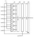
도 1은 반도체 장치의 회로도.
도 2는 타이밍 차트.
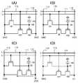
도 3의 (A) 내지 도 3의 (E)는 반도체 장치의 동작을 설명하는 도면.
도 4는 타이밍 차트.
도 5의 (A) 내지 도 5의 (D)는 반도체 장치의 동작을 설명하는 도면.
도 6은 반도체 장치의 회로도.
도 7은 행 선택 드라이버의 회로도.
도 8은 열 선택 드라이버의 회로도.
도 9는 A/D 컨버터의 회로도.
도 10은 반도체 장치의 회로도.
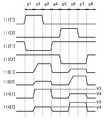
도 11은 타이밍 차트.
도 12는 타이밍 차트.
도 13의 (A) 내지 도 13의 (B)는 반도체 장치의 회로도.
도 14는 타이밍 차트.
도 15의 (A) 내지 도 15의 (E)는 반도체 장치의 동작을 설명하는 도면.
도 16은 타이밍 차트.
도 17의 (A) 내지 도 17의 (D)는 반도체 장치의 동작을 설명하는 도면.
도 18은 반도체 장치의 회로도.
도 19는 타이밍 차트.
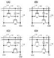
도 20의 (A) 내지 도 20의 (E)는 반도체 장치의 동작을 설명하는 도면.
도 21은 타이밍 차트.
도 22의 (A) 내지 도 22의 (D)는 반도체 장치의 동작을 설명하는 도면.
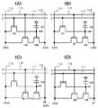
도 23의 (A) 및 도 23의 (B)는 반도체 장치의 회로도.
도 24는 타이밍 차트.
도 25의 (A) 내지 도 25의 (E)는 반도체 장치의 동작을 설명하는 도면.
도 26은 타이밍 차트.
도 27의 (A) 내지 도 27의 (D)는 반도체 장치의 동작을 설명하는 도면.
도 28은 반도체 장치의 단면도.
도 29의 (A) 및 도 29의 (B)는 트랜지스터의 단면도.
도 30의 (A) 내지 도 30의 (F)는 전자기기.1 is a circuit diagram of a semiconductor device;
2 is a timing chart.
3 (A) to 3 (E) are diagrams for explaining the operation of the semiconductor device.
4 is a timing chart.
FIGS. 5A to 5D are diagrams for explaining the operation of the semiconductor device; FIG.
6 is a circuit diagram of a semiconductor device.
7 is a circuit diagram of a row selection driver;
8 is a circuit diagram of a column select driver.
9 is a circuit diagram of an A / D converter.
10 is a circuit diagram of a semiconductor device.
11 is a timing chart.
12 is a timing chart.
13 (A) to 13 (B) are circuit diagrams of a semiconductor device.
14 is a timing chart.
FIGS. 15A to 15E are diagrams for explaining the operation of the semiconductor device; FIG.
16 is a timing chart.
FIGS. 17A to 17D are diagrams for explaining the operation of the semiconductor device; FIG.
18 is a circuit diagram of a semiconductor device.
19 is a timing chart.
20A to 20E are diagrams for explaining the operation of the semiconductor device.
21 is a timing chart.
Figures 22 (A) to 22 (D) are diagrams for explaining the operation of the semiconductor device.
23 (A) and 23 (B) are circuit diagrams of a semiconductor device.
24 is a timing chart.
FIGS. 25A to 25E are diagrams for explaining the operation of the semiconductor device; FIG.
26 is a timing chart.
27A to 27D are diagrams for explaining the operation of the semiconductor device.
28 is a sectional view of the semiconductor device;
29 (A) and 29 (B) are cross-sectional views of a transistor.
30 (A) to 30 (F) show electronic devices.
본 발명의 실시형태에 대하여, 도면을 참조하여 이하에 설명한다. 단, 본 발명은 이하의 설명에 한정되는 것은 아니다. 본 발명의 취지 및 그 범위로부터 벗어나지 않고, 그 형태 및 상세한 사항을 다양하게 변경할 수 있는 것은 당업자라면 용이하게 이해되기 때문이다. 따라서, 본 발명은 이하에 나타내는 실시형태의 기재 내용에만 한정하여 해석되는 것은 아니다. 단, 도면을 이용하여 본 발명의 구성을 설명함에 있어, 같은 것을 가리키는 부호는 다른 도면에서도 공통으로 이용한다.Embodiments of the present invention will be described below with reference to the drawings. However, the present invention is not limited to the following description. It is easily understood by those skilled in the art that various changes in form and detail can be made without departing from the spirit and scope of the present invention. Therefore, the present invention should not be construed as being limited to the description of the embodiments described below. In describing the configuration of the present invention with reference to the drawings, the same reference numerals are used in common to other drawings.
본 명세서에 있어서 "접속"은 전기적인 접속을 의미하고, 전류, 전압, 또는 전위를 공급할 수 있거나, 또는 전송 가능한 상태에 상당한다. 따라서, 접속하고 있는 상태란, 반드시 직접 접속하고 있는 상태를 가리키는 것은 아니고, 전류, 전압, 또는 전위를 공급 가능, 혹은 전송 가능하도록, 배선, 저항, 다이오드, 트랜지스터 등의 회로 소자를 통하여 전기적으로 접속하고 있는 상태도 그 범주에 포함한다.In this specification, "connection" means an electrical connection, and it can supply current, voltage, or electric potential, or corresponds to a state in which transmission is possible. Therefore, the state of connection does not necessarily indicate the state of directly connecting, but may be a state of electrically connecting through a circuit element such as a wire, a resistor, a diode, or a transistor so as to be capable of supplying or transmitting a current, a voltage, And the state in which they are doing is also included in that category.
본 명세서에 첨부한 도면에서는 구성 요소를 기능마다 분류하고, 서로 독립된 블록으로서 블럭도를 나타내고 있지만, 실제 구성 요소는 기능마다 완전하게 분리하는 것이 어렵고, 하나의 구성 요소가 복수의 기능과 관련된 것도 있을 수 있다.In the drawings attached hereto, the constituent elements are classified according to functions, and block diagrams are shown as independent blocks. Actual constituent elements are difficult to completely separate for each function, and one constituent element may be related to a plurality of functions .
단, 트랜지스터의 "소스"는 활성층으로서 기능하는 반도체막의 일부인 소스 영역, 혹은 상기 반도체막에 전기적으로 접속된 소스 전극을 의미한다. 마찬가지로, 트랜지스터의 "드레인"은 활성층으로서 기능하는 반도체막의 일부인 드레인 영역, 혹은 상기 반도체막에 전기적으로 접속된 드레인 전극을 의미한다. "게이트"는 게이트 전극을 의미한다.Note that the "source" of the transistor means a source region which is a part of the semiconductor film functioning as an active layer, or a source electrode electrically connected to the semiconductor film. Similarly, the "drain" of the transistor means a drain region which is a part of a semiconductor film functioning as an active layer, or a drain electrode electrically connected to the semiconductor film. "Gate" means a gate electrode.
트랜지스터가 갖는 "소스"와 "드레인"은 트랜지스터의 채널형 및 각 단자에 인가되는 전위의 높낮이에 의해, 그 부르는 방법이 바뀐다. 일반적으로, n채널형 트랜지스터에서는 낮은 전위가 인가되는 단자가 소스라고 불리고, 높은 전위가 인가되는 단자가 드레인이라고 불린다. 또한, p채널형 트랜지스터에서는 낮은 전위가 인가되는 단자가 드레인이라고 불리고, 높은 전위가 인가되는 단자가 소스라고 불린다. 본 명세서에서는, 편의상, 소스와 드레인이 고정되고 있는 것으로 가정하고, 트랜지스터의 접속 관계를 설명하는 경우가 있지만, 실제로는 상기 전위의 관계에 따라 소스와 드레인의 부르는 방법이 바뀐다.The "source" and "drain" of the transistor change depending on the channel type of the transistor and the height of the potential applied to each terminal. In general, in an n-channel transistor, a terminal to which a low potential is applied is called a source, and a terminal to which a high potential is applied is called a drain. In a p-channel transistor, a terminal to which a low potential is applied is called a drain, and a terminal to which a high potential is applied is called a source. In this specification, for convenience sake, it is assumed that the source and the drain are fixed and the connection relation of the transistors is described. Actually, the method of calling the source and the drain is changed according to the relation of the potential.
단, 어느 하나의 실시형태에서 설명하는 내용(일부의 내용이라도 좋음)은 그 실시형태에서 말하는 다른 내용(일부의 내용이라도 좋음), 또는/및 하나 또는 복수의 다른 실시형태에서 설명하는 내용(일부의 내용이라도 좋음)에 대하여, 적용, 조합, 또는 치환 등을 행할 수 있다.It is to be noted that the contents described in any one embodiment (some contents may be used) are not limited to the contents described in the embodiments (some contents may be used) and / or contents described in one or more other embodiments May be applied, combined, substituted, or the like to the content).
단, 도면에 있어서, 크기, 층의 두께, 또는 영역은 명료화를 위해 과장되어 있는 경우가 있다. 따라서, 반드시 그 스케일에 한정되지 않는다.However, in the drawings, the size, the layer thickness, or the area may be exaggerated for clarity. Therefore, it is not necessarily limited to the scale.
단, 도면은 이상적인 예를 모식적으로 나타낸 것이고, 도면에 나타내는 형상 또는 값 등에 한정되지 않는다. 예를 들면, 다음의 것들을 포함할 수 있다: 제조 기술에 의한 형상의 편차, 오차에 의한 형상의 편차, 노이즈에 의한 신호, 전압, 혹은 전류의 편차, 또는, 타이밍의 차이에 의한 신호, 전압, 혹은 전류의 편차 등을 포함할 수 있다.It should be noted, however, that the drawings are schematic representations of ideal examples and are not limited to the shapes or values shown in the drawings. For example, it may include the following: variations in shape due to manufacturing techniques, variations in shape due to errors, deviations in signals due to noise, variations in voltage or current, or differences in timing, Or current deviation.
전압은 어느 전위와 기준의 전위(예를 들면 접지 전위(GND) 또는 소스 전위)와의 전위차에 대한 것을 나타내는 경우가 많다. 따라서, 전압을 전위라고 바꿔 말할 수 있다. 여기서, 각 배선이나 각 단자의 전압은 상대적인 것이며, 어느 기준보다 높은 전압인지 낮은 전압인지가 중요해진다. 따라서, GND라고 기재되어 있어도 0 V로 한정되는 것은 아니다. 이것은 도면에서도 마찬가지이고, GND를 나타내는 부분이 있어도 0 V로 한정되지는 않는다.The voltage often indicates a potential difference between a certain potential and a reference potential (for example, ground potential (GND) or source potential). Therefore, the voltage can be referred to as a potential. Here, the voltage of each wiring and each terminal is relative, and it is important whether the voltage is higher or lower than a certain reference. Therefore, even if it is described as GND, it is not limited to 0 V. This also applies to the drawings, and even if there is a portion indicating GND, it is not limited to 0 V.
본 명세서에서는, "전기적으로 접속한다"라고 표현되는 경우에도, 현실의 회로에서는 물리적인 접속 부분이 없고, 배선이 연장되어 있을 뿐인 경우도 있다.In this specification, even when it is expressed as "electrically connected ", in a real circuit, there is no physical connection portion and the wiring is only extended.
또한, "제1", "제2"로 붙여지는 서수사는 편의상 이용하는 것이고, 공정 순서 또는 적층 순서를 나타내는 것은 아니다. 또한, 본 명세서에서 발명을 특정하기 위한 사항으로서 고유의 명칭을 나타내는 것은 아니다.The ordinal numbers assigned with "first" and "second" are used for convenience, and do not indicate a process order or a stacking order. In addition, the specification does not show a unique name as an item for specifying the invention.
단, "반도체"라고 표기한 경우에도, 예를 들면, 도전성이 충분히 낮은 경우는 "절연체"로서의 특성을 갖는 경우가 있다. 또한, "반도체"와 "절연체"는 경계가 애매하고, 엄밀하게 구별할 수 없는 경우가 있다. 따라서, 본 명세서에 기재된 "반도체"는 "절연체"로 바꿔 말할 수 있는 경우가 있다. 마찬가지로, 본 명세서에 기재된 "절연체"는 "반도체"로 바꿔 말할 수 있는 경우가 있다.However, even when the word "semiconductor" is written, for example, when the conductivity is sufficiently low, there is a case where the semiconductor device has characteristics as an "insulator ". Further, the "semiconductor" and the "insulator" sometimes have vagueness and can not be distinguished precisely. Thus, the term " semiconductor "described herein may be referred to as an" insulator ". Likewise, the term "insulator" described herein may be referred to as "semiconductor ".
또한, "반도체"라고 표기한 경우에도, 예를 들면, 도전성이 충분히 높은 경우는 "도전체"로서의 특성을 갖는 경우가 있다. 또한, "반도체"와 "도전체"는 경계가 애매하고, 엄밀하게 구별할 수 없는 경우가 있다. 따라서, 본 명세서에 기재된 "반도체"는 "도전체"로 바꿔 말할 수 있는 경우가 있다. 마찬가지로, 본 명세서에 기재된 "도전체"는 "반도체"로 바꿔 말할 수 있는 경우가 있다.Further, even when the word "semiconductor" is written, for example, when the conductivity is sufficiently high, there are cases where the semiconductor device has characteristics as a "conductor ". In addition, the "semiconductor" and the "conductor" may have a vague boundary and can not be distinguished precisely. Thus, the term " semiconductor "as used herein may be referred to as" conductor ". Likewise, "conductors" described herein may be referred to as "semiconductors ".
본 명세서에서, "평행"이란, 2개의 직선이 -10° 이상 10° 이하의 각도로 배치되어 있는 상태를 말하고, 따라서, -5° 이상 5° 이하의 경우도 포함된다. 또한, "수직"이란, 2개의 직선이 80° 이상 100° 이하의 각도로 배치되어 있는 상태를 말하고, 따라서, 85° 이상 95° 이하의 경우도 포함된다.In the present specification, "parallel" refers to a state in which two straight lines are arranged at an angle of not less than -10 DEG and not more than 10 DEG, and therefore includes not more than -5 DEG and not more than 5 DEG. The term "vertical" refers to a state in which two straight lines are arranged at an angle of 80 DEG or more and 100 DEG or less, and therefore, the case of 85 DEG or more and 95 DEG or less is also included.
본 명세서에 있어서, 결정이 삼방정 또는 능면체정인 경우, 육방정계로서 나타낸다.In the present specification, when the crystal is a trigonal or rhombohedral, it is represented as a hexagonal system.
(실시형태 1)(Embodiment 1)
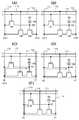
도 1에 반도체 장치(100)를 나타낸다. 반도체 장치(100)는 트랜지스터(101), 트랜지스터(102), 용량 소자(103)를 포함한다. 반도체 장치(100)는 메모리 셀로서 기능할 수 있기 때문에, 반도체 장치(100)를 메모리 셀(100)이라고 하는 경우도 있다.Fig. 1 shows a
트랜지스터(101)의 채널이 형성되는 영역은 산화물 반도체층을 포함한다. 트랜지스터(101)는 산화물 반도체층을 포함한다. 따라서, 트랜지스터(101)는 오프 전류가 매우 낮다는 특성을 가진다.The region where the channel of the
트랜지스터(101)는 n형 또는 p형의 트랜지스터이다. 이하에서는 n형인 경우에 대하여 설명한다.The
트랜지스터(101)의 게이트는 배선(111)에 전기적으로 접속된다. 배선(111)은 워드선으로서 기능할 수 있다.The gate of the
트랜지스터(101)의 소스 및 드레인의 한쪽은 배선(113)에 전기적으로 접속된다. 배선(113)은 비트선으로서 기능할 수 있다.One of the source and the drain of the
트랜지스터(101)의 소스 및 드레인의 다른 한쪽은 용량 소자(103)의 한쪽의 전극에 전기적으로 접속된다. 트랜지스터(101)의 소스 및 드레인의 다른 한쪽은 트랜지스터(102)의 게이트에 전기적으로 접속된다.The other of the source and the drain of the
트랜지스터(102)의 채널이 형성되는 영역은 산화물 반도체, 실리콘 등 다양한 재료를 갖는 층을 이용할 수 있다. 트랜지스터(102)는 p형의 트랜지스터이다.As the region where the channel of the
트랜지스터(102)의 소스 및 드레인의 한쪽은 배선(114)에 전기적으로 접속된다. 배선(114)은 신호선, 소스선 또는 전원선으로서 기능할 수 있다.One of the source and the drain of the
트랜지스터(102)의 소스 및 드레인의 다른 한쪽은 배선(113)에 전기적으로 접속된다. 트랜지스터(102)의 소스 및 드레인의 다른 한쪽은 트랜지스터(101)의 소스 및 드레인의 한쪽에 전기적으로 접속된다.The other of the source and the drain of the
용량 소자(103)의 한쪽의 전극은 트랜지스터(101)의 소스 및 드레인의 다른 한쪽에 전기적으로 접속된다. 용량 소자(103)의 한쪽의 전극은 트랜지스터(102)의 게이트에 전기적으로 접속된다.One electrode of the
용량 소자(103)의 다른 한쪽의 전극은 배선(112)에 전기적으로 접속된다. 배선(112)은 용량선으로서 기능할 수 있다.The other electrode of the
반도체 장치(100)로의 데이터의 기록 동작 및 반도체 장치(100)로부터의 데이터의 판독 동작을 설명한다.The operation of writing data into the
(기록 동작)(Write operation)
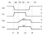
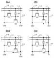
먼저, 기록 동작의 일례를 설명한다. 도 2에 타이밍 차트를 나타낸다. 도 3의 (A) 내지 도 3의 (E)에 반도체 장치(100)의 동작을 나타낸다. 일례로서 판독하고자 하는 전압을 V1으로 하고, 노드(104)의 전위(트랜지스터(102)의 게이트 전위)를 V2까지 변화시킴으로써, 데이터를 기록하는 동작을 설명한다. 멀티 비트 데이터를 저장할 때에는 다양한 전압을 인가할 필요가 있기 때문에, V1을 자유롭게 설정할 수 있는 점에서 유익하다.First, an example of the recording operation will be described. A timing chart is shown in Fig. 3 (A) to 3 (E) show the operation of the
데이터를 기록하는 동작은 제1 스텝 및 제2 스텝에 의해 행해진다. 제1 스텝에서, 배선(113) 및 배선(114)에 저전압을 인가하고, 배선(111)에 고전압을 인가하고 트랜지스터(101)를 온으로 하고, 또한, 배선(112)에 저전압을 인가하여 트랜지스터(102)를 온으로 한다. 제2 스텝에서, 배선(114)에 전압(V1)을 인가하고, 또한 배선(113)에 대한 저전압의 인가를 차단한다.An operation of recording data is performed by a first step and a second step. In the first step, a low voltage is applied to the
제2 스텝에 의해, 배선(114)으로부터, 트랜지스터(102)의 소스 및 드레인, 배선(113), 및 트랜지스터(101)의 소스 및 드레인을 통하여, 노드(104)에 데이터(전압(V1))에 따른 전위(V2)가 인가된다. 그리고 트랜지스터(102)의 게이트에 V2가 인가된다. 용량 소자(103)에는 V2에 따른 전하가 축적된다.(Voltage V1) is supplied to the
도 3의 (A)에 반도체 장치(100)의 초기 상태를 나타낸다. 도 2에서는 초기 상태를 (A)로 나타낸다.3A shows an initial state of the
배선(111)에 저전압(L전압이라고도 함)의 신호가 입력되어 있고, 트랜지스터(101)는 오프한다. 상기 저전압은 트랜지스터(101)를 오프할 수 있는 전압이면 좋다. 상기 저전압은 기준 전압(GND)이어도 좋고, 전원 전압(VDD 또는 VSS), 그 외의 전압이어도 좋다.A signal of a low voltage (also referred to as L voltage) is input to the
배선(112)에는 고전압(H전압이라고도 함)의 신호가 입력된다. 노드(104)에는 용량 소자(103)의 용량치에 대응한 전압이 인가되어 트랜지스터(102)는 오프한다. 상기 고전압은 트랜지스터(102)를 오프할 수 있는 전압이면 좋다. 상기 고전압은 전원 전압(VDD)이나 그 외의 전압이어도 좋다.A signal of a high voltage (also referred to as H voltage) is input to the
배선(113) 및 배선(114)에 저전압(GND)이 인가된다. 이것에 의해 배선(113) 및 배선(114)에 저전압을 프리차지(pre-charge)할 수 있다. 여기에서는 저전압은 기준 전압(GND)으로 했지만, 전원 전압(VSS)이나 그 외의 전압이어도 좋다.A low voltage (GND) is applied to the
도 3의 (B)에 기록 전의 준비 상태를 나타낸다. 도 2에서는 상기 상태를 (B)로 나타낸다.FIG. 3 (B) shows the ready state before writing. In Fig. 2, this state is shown by (B).
시각 t1에서 배선(111)에 고전압의 신호가 입력된다. 트랜지스터(101)는 온한다. 상기 고전압은 트랜지스터(101)를 온할 수 있는 전압이면 좋다. 상기 고전압은 전원 전압(VDD)이나 그 외의 전압이어도 좋다.At time t1, a high-voltage signal is input to the
트랜지스터(101)가 온함으로써, 배선(113)과 노드(104)는 전기적으로 접속된다. 노드(104)의 전위는 저하되어 전압(GND)이 된다.When the
시각 t1에서 배선(112)에 저전압의 신호가 입력된다. 노드(104)에는 용량 소자(103)의 용량치에 대응한 전압이 인가된다. 트랜지스터(101)가 온하고, 배선(112)에 저전압이 인가되어, 트랜지스터(102)는 온한다. 상기 저전압은 트랜지스터(102)를 온할 수 있는 전압이면 좋다. 상기 저전압은 기준 전압(GND), 전원 전압(VSS)이나 그 외의 전압이어도 좋다.At time t1, a low-voltage signal is input to the
배선(113) 및 배선(114)에 저전압이 인가되고 트랜지스터(101) 및 트랜지스터(102)가 온한다. 제1 스텝이 종료된다.A low voltage is applied to the
도 3의 (C), 도 3의 (D)에 기록 시의 상태를 나타낸다. 도 2에서는 상기 상태를 (C), (D)로 나타낸다.3 (C) and 3 (D) show the state at the time of recording. 2 (C) and (D).
시각 t2에서 배선(114)에 전압(V1)을 인가한다(도 3의 (C)). 전압(V1)은 판독 동작 시에 판독하고자 하는 전압이다. V1의 크기는 기록하고자 하는 데이터에 맞추어 자유롭게 설정할 수 있다.At time t2, the voltage V1 is applied to the wiring 114 (Fig. 3 (C)). Voltage V1 is the voltage to be read in the read operation. The size of V1 can be freely set according to the data to be recorded.
시각 t2에서 배선(113)으로의 저전압(GND)의 공급을 차단한다(도 3의 (C)). 이 때, 배선(113)은 프리차지된 전압으로부터, 전기적으로 부유 상태가 된다. 즉, 배선(113)은 전하의 충전 또는 방전에 의해 전위의 변동이 용이하게 발생하는 상태가 된다. 이 부유 상태는 배선(113)에 전위를 공급하는 스위치를 오프로 함으로써 실현할 수 있다.At time t2, the supply of the low voltage (GND) to the
트랜지스터(102)가 온하고 있기 때문에, 배선(113)은 배선(114)과 전기적으로 접속된다. 배선(113)의 전압은 프리차지된 저전압(GND)으로부터 V2'까지 변화한다(도 3의 (D)). 단, V2'는 V1과 대략 트랜지스터(102)의 문턱 전압만큼 다르다.Since the
트랜지스터(101)가 온하고 있기 때문에, 배선(114)으로부터 트랜지스터(102)의 소스 및 드레인, 배선(113), 및 트랜지스터(101)의 소스 및 드레인을 통하여, 노드(104)(트랜지스터(102)의 게이트)에 데이터가 기록된다. 용량 소자(103)에 전하가 축적된다. 그리고 노드(104)의 전위는 V2까지 변화한다.The node 104 (the transistor 102) is connected from the
노드(104)의 전위가 V2까지 변화되면, 트랜지스터(102)의 게이트와 소스 사이의 전위차가 작아져; 트랜지스터(102)의 소스와 드레인 사이를 흐르는 전류(Id)는 작아진다. 최종적으로 트랜지스터(102)는 오프한다.When the potential of the
반도체 장치(100)에서는, 배선(114)에는 V1이 인가되고, 배선(113)에는 V2'가 인가되고, 노드(104)에는 V2가 인가된 상태가 된다.In the
배선(114)에 전압(V1)이 인가되고, 배선(113)에 대한 저전압의 인가가 차단되어, 제2 스텝이 종료된다.The voltage V1 is applied to the
이상에 의해, 판독하고자 하는 전압(V1)을 배선(114)에 인가하고, 노드(104)의 전위를 V2까지 변화시킴으로써 기록 동작이 종료된다.Thus, the writing operation is ended by applying the voltage V1 to be read to the
도 3의 (E)에 기록 후, 유지 전의 상태를 나타낸다. 도 2에서는 상기 상태를 (E)로 나타낸다.FIG. 3 (E) shows the state before recording, after recording. In Fig. 2, this state is indicated by (E).
시각 t3에서 배선(111)에 저전압의 신호가 입력된다. 트랜지스터(101)는 오프한다. 노드(104)는 배선(113)과 전기적으로 접속되지 않은 상태가 된다. 트랜지스터(101)는 오프 전류가 매우 낮다는 특성을 가지기 때문에, 노드(104)의 전위(V2)는 유지된다.At time t3, a low-voltage signal is input to the
시각 t4까지의 동안에, 배선(112)에 고전압이 인가되고, 배선(113)에 저전압(GND)이 인가되고, 배선(114)에 저전압(GND)이 인가된다.A high voltage is applied to the
배선(112)에 고전압이 인가되면, 노드(104)의 전위는 V2로부터 트랜지스터(102)를 오프할 수 있는 전압까지 변화한다.When a high voltage is applied to the
시각 t4에는 유지 상태가 된다. 도 2에서는 상기 상태를 (F)로 나타낸다. 반도체 장치(100)는 노드(104)의 전위가 다른 점을 제외하고, 도 3의 (A)와 같은 상태가 된다. 트랜지스터(101)는 오프한다.At time t4, the holding state is established. In Fig. 2, this state is indicated by (F). The
단, 도 2의 (A), 도 2의 (F) 상태에서는, 배선(114)에 저전압을 인가하고 있지만, 고전압을 인가해도 좋다. 배선(114)에 고전압을 인가해 두면, (E) 상태로부터 (F) 상태, 즉 배선(114)에 고전압을 인가할 때에, 신속하게 전압을 변화시킬 수 있는 경우가 있다.2 (A) and 2 (F), although a low voltage is applied to the
(판독 동작)(Read operation)
다음에, 상기 기록 동작에 의해, 기록된 전하로부터, 전압(V1)을 판독하는 동작의 일례를 설명한다. 도 4에 타이밍 차트를 나타낸다. 도 5의 (A) 내지 도 5의 (D)에 반도체 장치(100)의 동작을 나타낸다.Next, an example of an operation of reading the voltage V1 from the recorded electric charges by the above-described writing operation will be described. Fig. 4 shows a timing chart. Figs. 5A to 5D show the operation of the
데이터를 판독하는 동작은 배선(114)에 고전압을 인가하는 제3 스텝, 배선(114)에의 고전압의 인가를 차단하고, 또한 배선(112)에 저전압을 인가하는 제4 스텝에 의해 행해진다. 제4 스텝에 의해, 배선(114)의 전압은 고전압으로부터 전압(V1)으로 변화한다.The data reading operation is performed by a third step of applying a high voltage to the
도 5의 (A)에 반도체 장치(100)의 유지 상태를 나타낸다. 도 4에서는 유지 상태를 (A)로 나타낸다.Fig. 5A shows the holding state of the
도 5의 (B)에 판독하기 전의 준비 상태를 나타낸다. 도 4에서는 상기 상태를 (B)로 나타낸다.FIG. 5B shows a ready state before reading. In Fig. 4, this state is shown by (B).
시각 t5에서 배선(114)에 고전압(VDD)이 인가된다. 배선(114)에 고전압을 프리차지할 수 있다. 여기에서는 고전압은 전원 전압(VDD)으로 했지만, 그 외의 전압이어도 좋다. 다만 상기 고전압은 V1보다 높은 것이 바람직하다.At time t5, the high voltage VDD is applied to the
단, 트랜지스터(101) 및 트랜지스터(102)는 유지 상태로부터 오프한 상태이다.However, the
배선(114)에 고전압이 인가되어, 제3 스텝이 종료된다.A high voltage is applied to the
도 5의 (C), 도 5의 (D)에 판독 시의 상태를 나타낸다. 도 4에서는 상기 상태를 (C)로 나타낸다.Fig. 5C and Fig. 5D show the state at the time of reading. In Fig. 4, this state is indicated by (C).
시각 t6에서 배선(114)으로의 고전압(VDD)의 공급을 차단한다(도 5의 (C)). 이 때, 배선(114)은 프리차지된 전압으로부터, 전기적으로 부유 상태가 된다. 즉, 배선(114)은 전하의 충전 또는 방전에 의해 전위의 변동이 용이하게 발생하는 상태가 된다. 이 부유 상태는 배선(114)에 전위를 공급하는 스위치를 오프로 함으로써 실현할 수 있다.At time t6, supply of the high voltage VDD to the
시각 t6에서 배선(112)에 저전압의 신호가 입력된다. 노드(104)의 전위는 기록 시의 V2까지 변화한다. 그 결과, 트랜지스터(102)의 게이트 전위(V2)와 배선(114)의 전위에 대응한 전류(Id)가 흐른다. 단, 배선(112)에 입력되는 저전압은 기록 동작 시에 배선(112)에 입력된 저전압과 같은 전압인 것이 바람직하다.At time t6, a low-voltage signal is input to the
배선(114)의 전위는 게이트 전압(V2)에 대응하고, 프리차지된 고전압(VDD)으로부터 V1까지 변화한다(도 5의 (D)). 트랜지스터(102)의 게이트와 소스 사이의 전위차는 시간 경과와 함께 작아지고, 최종적으로는 트랜지스터(102)는 오프한다.The potential of the
배선(114)을 판별 회로 등에 전기적으로 접속시켜 V1을 판독한다. 이것에 의해 전압(V1)을 판독할 수 있다.The
배선(114)에 대한 고전압의 인가가 차단되고, 또한 배선(112)에 저전압이 인가된다. 따라서, 제4 스텝이 종료된다.The application of the high voltage to the
판독 후, 시각 t7에서 배선(112)에 고전압의 신호가 입력된다. 배선(112)에 고전압이 인가되면, 노드(104)의 전위는 V2로부터 상기 고전압만큼 변화한다. 따라서, 트랜지스터(102)는 오프한다.After reading, a high-voltage signal is input to the
시각 t8까지의 동안에, 배선(114)에 저전압(GND)이 인가된다.During time t8, a low voltage (GND) is applied to the
시각 t8에는 유지 상태가 된다. 도 4에서는 상기 상태를 (E)로 나타낸다. 반도체 장치(100)는 도 5의 (A)와 같은 상태가 된다.At time t8, the holding state is established. In Fig. 4, this state is indicated by (E). The
단, 도 4의 (A), 도 4의 (E) 상태에서는 배선(114)에 저전압을 인가하고 있지만, 고전압을 인가해도 좋다. 배선(114)에 고전압을 인가해 두면, (A) 상태로부터 (B) 상태, 즉 배선(114)에 VDD를 인가할 때에, 신속하게 전압을 변화시킬 수 있다.4 (A) and 4 (E), although the low voltage is applied to the
단, 노드(104)의 전위, 즉 트랜지스터(102)의 게이트에 인가된 전위를 리셋하는 경우는, 예를 들면 배선(112)에 저전압을 인가하고, 또한 배선(111)에 고전압의 신호를 입력하여 트랜지스터(101)를 온으로 한다. 따라서, 트랜지스터(101)가 온이 되면, 노드(104)는 배선(113)과 전기적으로 접속된다. 배선(113)에는 GND가 인가되어 있기 때문에, 노드(104)의 전위는 리셋된다.However, when resetting the potential of the
본 실시형태에서는, 기록 시에 배선(114)에 인가한 전위(V1)가 그대로 판독 전위가 된다.In the present embodiment, the potential V1 applied to the
종래, 판독 전압에는 분포가 발생되어 있었다. 예를 들면 V1이 판독하고자 하는 전압이었다고 해도, 판독 트랜지스터의 문턱의 편차 등의 영향에 의해, 실제로는 판독 전압은 V1±ΔV로 되어 있었다. 즉 판독 전압은 ΔV의 확산을 갖고 있었다. 그러나 본 실시형태에서는, 배선(114)에 원하는 전위(V1)을 인가하여, 상기 전위(V1)을 판독할 수 있게 된다. 따라서 ΔV를 작게 할 수 있어, 판독 전압의 분포의 폭을 작게 할 수 있다.Conventionally, a distribution has been generated in the read voltage. For example, even if V1 is the voltage to be read, the read voltage is actually V1 ± ΔV due to the influence of the deviation of the threshold of the read transistor and the like. That is, the read voltage had a diffusion of? V. However, in the present embodiment, the desired potential V1 is applied to the
반도체 장치(100)에 멀티 비트 데이터를 저장시키는 경우에는, 원하는 전압을, 정확하게 기록하고, 정확하게 판독할 필요가 있다. 따라서 높은 정밀도가 요구된다. 그러나 본 실시형태에서는, 원하는 전위를 인가하고, 상기 전위를 판독할 수 있다. 따라서 멀티 비트 데이터를 저장할 때, 반도체 장치(100)는 높은 유지 특성과 고신뢰성을 가진다.When storing the multi-bit data in the
종래, 정확하게 기록이 행해지고 있는지를 확인하기 위해, 검증 동작을 행하고 있었다. 그러나 본 실시형태에서는, 검증 동작은 불필요해진다. 이것에 의해 고속 동작이 가능해진다.Conventionally, a verification operation is performed to confirm whether or not recording is performed accurately. However, in the present embodiment, the verification operation becomes unnecessary. This enables high-speed operation.
본 실시형태는 다른 실시형태의 기재와 적절히 조합시킬 수 있다.This embodiment mode can be appropriately combined with the description of another embodiment mode.
(실시형태 2)(Embodiment 2)
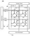
본 실시형태에서는 도 1에 설명한 구동 방법을 행할 수 있는 반도체 장치의 일례에 대하여 설명한다. 또한, 이하에서는, 도 6, 도 7, 도 8, 도 9, 도 10, 도 11 및 도 12를 참조하여 설명한다.In the present embodiment, an example of a semiconductor device capable of performing the driving method shown in Fig. 1 will be described. 6, 7, 8, 9, 10, 11, and 12. FIG.
(반도체 장치의 구성예)(Configuration Example of Semiconductor Device)
도 1에 설명한 메모리 셀(100)을 갖는 반도체 장치(200)의 구성예를 나타내는 블럭도를 도 6에 도시한다.FIG. 6 is a block diagram showing a configuration example of a
도 6에 나타내는 반도체 장치(200)는 도 1에 설명한 메모리 셀(100)이 복수 제공된 메모리 셀 어레이(201), 행 선택 드라이버(202), 열 선택 드라이버(203), 및 A/D 컨버터(204)를 포함한다. 단, 반도체 장치(200)는 m행 n열의 매트릭스 모양으로 배열된 메모리 셀(100)을 포함한다. 도 6에서는 배선(111)으로서, (m-1)번째 행의 배선(111)[m-1] 및 m번째 행의 배선(111)[m]이 제공된다. 배선(112)으로서, (m-1)번째 행의 배선(112)[m-1] 및 m번째 행의 배선(112)[m]이 제공된다. 배선(113)으로서, (n-1)번째 열의 배선(113)[n-1] 및 n번째 열의 배선(113)[n]이 제공된다. 배선(114)으로서, (n-1)번째 열의 배선(114)[n-1] 및 n번째 배선(114)[n]이 제공된다.The
도 6에 나타내는 메모리 셀 어레이(201)는 도 1에 설명한 메모리 셀(100)이 매트릭스 모양으로 배열된다. 단, 메모리 셀(100)에 포함되는 각 구성의 설명은 도 1과 마찬가지이고, 따라서, 생략한다. 설명은 도 1에서의 설명을 원용하는 것으로 한다.In the
행 선택 드라이버(202)는 메모리 셀(100)의 각 행에서의 트랜지스터(101)를 선택적으로 도통 상태로 하는 기능, 및 메모리 셀(100)의 각 행에서의 노드(104)의 전위를 선택적으로 변화시키는 기능을 구비한 회로이다. 구체적으로는, 배선(111)에 신호를 공급하고, 배선(112)에 신호를 공급하는 회로이다. 행 선택 드라이버(202)를 구비함으로써, 반도체 장치(200)는 메모리 셀(100)로의 데이터의 기록 및 판독을 행마다 선택하여 행할 수 있다.The
열 선택 드라이버(203)는 메모리 셀(100)의 배선(113), 배선(114)의 전위를 프리차지하는 기능, 배선(113), 배선(114)의 전위를 초기화하는 기능, 및 배선(113), 배선(114)을 전기적으로 부유 상태로 하는 기능을 구비한 회로이다. 열 선택 드라이버(203)를 구비함으로써, 반도체 장치(200)는 메모리 셀(100)로의 데이터의 기록 및 판독을 열마다 선택하여 행할 수 있다.The
A/D 컨버터(204)는 아날로그치인 배선(114)의 전위를 디지털값으로 변환하여 외부로 출력하는 기능을 구비한 회로이다. 구체적으로는, 플래시형의 A/D 컨버터를 포함하는 회로이다. A/D 컨버터(204)를 구비함으로써, 반도체 장치(200)는 메모리 셀(100)로부터 판독된 데이터에 대응하는 배선(114)의 전위를 외부에 출력할 수 있다.The A /
단, A/D 컨버터(204)는 플래시형의 A/D 컨버터로서 설명을 행한다. 그러나, 순서대로 비교형, 멀티 슬로프형, 델타 시그마형의 A/D 컨버터를 이용해도 좋다.However, the A /
(행 선택 드라이버의 구성예)(Example of configuration of row selection driver)
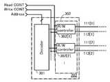
도 6에 설명한 행 선택 드라이버(202)의 구성예를 나타내는 블럭도를 도 7에 도시한다.FIG. 7 is a block diagram showing a configuration example of the
도 7에 나타내는 행 선택 드라이버(202)는 디코더(301) 및 제어 회로(302)를 포함한다. 제어 회로(302)는 배선(111) 및 배선(112)의 행마다 제공된다. 첫번째 행에는 제어 회로(302)[1](도 7에서는 R/W controller라고 표기함)가 제공된다. 두번째 행에는 제어 회로(302)[2]가 제공된다. 각 행의 제어 회로(302)는 배선(111), 및 배선(112)에 접속된다.The
디코더(301)는 배선(111) 및 배선(112)이 제공되는 행을 선택하기 위한 신호를 출력하는 기능을 구비한 회로이다.The
제어 회로(302)는 디코더(301)로 선택된 배선(111) 및 배선(112)이 제공된 행에 신호를 출력하는 기능을 구비한 회로이다.The
(열 선택 드라이버의 구성예)(Example of configuration of column select driver)
도 6에 설명한 열 선택 드라이버(203)의 구성예를 나타내는 블럭도를 도 8에 도시한다.Fig. 8 is a block diagram showing a configuration example of the
도 8에 나타내는 열 선택 드라이버(203)는 디코더(401), 래치 회로(402), D/A 컨버터(403), 스위치 회로(404), 트랜지스터(405), 및 트랜지스터(406)를 포함한다. 상술한 디코더(401), 래치 회로(402), D/A 컨버터(403), 스위치 회로(404), 트랜지스터(405), 및 트랜지스터(406)는 열마다 제공된다. 각 열의 스위치 회로(404), 트랜지스터(405), 및 트랜지스터(406)는 배선(114)에 접속된다.The
디코더(401)는 배선(114)이 제공되는 열을 선택하고, 입력되는 데이터를 배분하여 출력하는 기능을 구비한 회로이다. 구체적으로는, 어드레스 신호(Address) 및 데이터(Data)가 입력되고, 이 어드레스 신호(Address)에 따라 어느 행의 래치 회로(402)에 데이터(Data)를 출력하는 회로이다. 디코더(401)를 구비함으로써, 열 선택 드라이버(203)는 임의의 열을 선택하여, 데이터의 기록을 행할 수 있다.The
단, 디코더(401)에 입력되는 데이터(Data)는 k 비트의 디지털 데이터이다. k 비트의 디지털 데이터는 비트마다 '1' 또는 '0'의 2치의 데이터로 나타내는 신호이다. 예를 들어, 2 비트의 디지털 데이터이면, '00', '01', '10', '11'로 나타내는 데이터이다.However, the data (Data) input to the
래치 회로(402)는 입력되는 데이터(Data)를 일시적으로 저장하는 기능을 구비한 회로이다. 구체적으로는, 래치 신호(W_LAT)가 입력되고, 이 래치 신호(W_LAT)에 따라 저장한 데이터(Data)를 D/A 컨버터(403)에 출력하는 플립 플롭 회로이다. 래치 회로(402)를 구비함으로써, 열 선택 드라이버(203)는 임의의 타이밍에 데이터의 기록을 행할 수 있다.The
D/A 컨버터(403)는 입력되는 디지털값의 데이터(Data)를 아날로그치의 데이터(Vdata)로 변환하는 기능을 구비한 회로이다. 구체적으로 D/A 컨버터(403)는 데이터(Data)의 비트수가 3 비트이면, 복수의 전위(V0) 내지 전위(V7)의 8 단계의 전위 중 어느 하나로 변환하고, 스위치 회로(404)에 출력하는 회로이다. D/A 컨버터(403)를 구비함으로써, 열 선택 드라이버(203)는 메모리 셀(100)에 기록하는 데이터를 멀티 비트의 데이터에 대응하는 전위로 할 수 있다.The D /
단, D/A 컨버터(403)로부터 출력되는 Vdata는 다른 전압치로 나타내는 데이터이다. 2 비트의 데이터로 말하면, 예를 들면 0.5 V, 1.0 V, 1.5 V, 2.0 V의 4치의 데이터가 되고, 어느 하나의 전압치로 나타내는 데이터라고 할 수 있다.However, Vdata output from the D /
스위치 회로(404)는 입력되는 데이터 Vdata를 배선(114)에 공급하는 기능, 및 배선(114)을 전기적으로 부유 상태로 하는 기능을 구비한 회로이다. 구체적으로는, 아날로그 스위치와 인버터를 구비하고 스위치 제어 신호(Write_SW)에 의한 제어에 의해, 데이터(Vdata)를 배선(114)에 공급하고, 그 후 아날로그 스위치를 오프로 함으로써 전기적으로 부유 상태로 하는 회로이다. 스위치 회로(404)를 구비함으로써, 열 선택 드라이버(203)는 데이터(Vdata)를 배선(114)에 공급한 후, 배선(114)을 전기적으로 부유 상태로 유지할 수 있다.The
트랜지스터(405)는 프리차지 전압(VDD)을 배선(114)에 공급하는 기능, 및 배선(114)을 전기적으로 부유 상태로 하는 기능을 구비한 트랜지스터이다. 구체적으로는, 프리차지 제어 신호(Pre_EN)에 의한 제어로 프리차지 전압(VDD)을 배선(114)에 공급하고, 그 후, 배선(114)을 전기적으로 부유 상태로 하는 스위치이다. 트랜지스터(405)를 구비함으로써, 열 선택 드라이버(203)는 프리차지 전압(VDD)을 배선(114)에 공급한 후, 배선(114)을 전기적으로 부유 상태로 유지할 수 있다.The
트랜지스터(406)는 초기화 전압(GND)을 배선(114)에 공급하는 기능을 구비한 트랜지스터이다. 구체적으로는, 초기화 제어 신호(Init_EN)에 의한 제어로 초기화 전압(GND)을 배선(114)에 공급하는 스위치이다. 트랜지스터(406)를 구비함으로써, 열 선택 드라이버(203)는 초기화 전압(GND)을 배선(114)에 공급할 수 있다.The
단, 도시하지 않았지만, 열 선택 드라이버(203)는 배선(113)에 프리차지 전압(GND)을 인가하고, 또한 배선(113)을 전기적으로 부유 상태로 하는 기능을 가진다. 이러한 기능은 배선(114)과 같은 구성을 가짐으로써 행할 수 있기 때문에; 배선(114)의 기재를 원용한다.Although not shown, the
(A/D 컨버터의 구성예)(Configuration example of A / D converter)
도 6에 설명한 A/D 컨버터(204)의 구성예를 나타내는 블럭도를 도 9에 도시한다.FIG. 9 is a block diagram showing a configuration example of the A /
도 9에 도시하는 A/D 컨버터(204)는 콤퍼레이터(501), 인코더(502), 래치 회로(503), 및 버퍼(504)를 포함한다. 콤퍼레이터(501), 인코더(502), 래치 회로(503), 및 버퍼(504)는 열마다 제공된다. 각 열의 버퍼(504)는 데이터(Dout)를 출력한다.The A /
콤퍼레이터(501)는 배선(114)의 전위와, 참조 전압(Vref0) 내지 참조 전압(Vref6)과의 전위의 높낮이를 비교하고, 배선(114)의 전위가 멀티 비트의 데이터 중 어느 것에 따른 전위인지를 판정하는 기능을 구비한 회로이다. 구체적으로는, 복수의 콤퍼레이터를 포함하고, 각각의 콤퍼레이터(501)에 배선(114)의 전위와, 다른 참조 전압(Vref0) 내지 참조 전압(Vref6)이 공급되고, 배선(114)의 전위가 어느 전위의 사이에 있는지를 판정하는 회로이다. 콤퍼레이터(501)를 구비함으로써, A/D 컨버터(204)는 배선(114)의 전위가 멀티 비트의 데이터 중 어느 것에 대응하는 전위인지를 판정할 수 있다.The
단, 일례로서 도 9에 도시하는 참조 전압(Vref0) 내지 참조 전압(Vref6)은 멀티 비트의 데이터가 3 비트, 즉 8치의 데이터인 경우에 공급되는 전위이다.However, as an example, the reference voltages Vref0 to Vref6 shown in Fig. 9 are potentials supplied when the multi-bit data is 3-bit data, that is, 8-value data.
인코더(502)는 콤퍼레이터(501)로부터 출력되는 배선(114)의 전위를 판정하는 신호를 기초로, 다비트의 디지털 신호를 생성하는 기능을 구비한 회로이다. 구체적으로는, 복수의 콤퍼레이터로부터 출력되는 H 레벨 또는 L 레벨의 신호를 기초로 부호화를 행하여, 디지털 신호를 생성하는 회로이다. 인코더(502)를 구비함으로써, A/D 컨버터(204)는 메모리 셀(100)로부터 판독된 데이터를 디지털값의 데이터로 할 수 있다.The
래치 회로(503)는 입력되는 디지털값의 데이터를 일시적으로 저장하는 기능을 구비한 회로이다. 구체적으로는, 래치 신호(LAT)가 입력되고, 이 래치 신호(LAT)에 따라 저장된 데이터를 버퍼(504)에 출력하는 플립 플롭 회로이다. 래치 회로(503)를 구비함으로써, A/D 컨버터(204)는 임의의 타이밍에 데이터의 출력을 행할 수 있다. 단, 래치 회로(503)는 생략할 수 있다.The
버퍼(504)는 래치 회로(503)로부터 출력된 데이터를 증폭하고, 출력 신호(Dout)로서 출력하는 기능을 구비한 회로이다. 구체적으로는, 인버터 회로를 짝수단 포함한 회로이다. 버퍼(504)를 구비함으로써, A/D 컨버터(204)는 디지털 신호에 대한 노이즈를 저감할 수 있다. 단, 버퍼(504)는 생략할 수 있다.The
(반도체 장치의 구동 방법의 구체적인 예)(Specific example of driving method of semiconductor device)
도 10에는 반도체 장치가 갖는 메모리 셀의 회로도를 나타낸다. 도 11 및 도 12에 나타내는 타이밍 차트도는 도 10의 동작을 설명하는 것이다.10 shows a circuit diagram of a memory cell included in the semiconductor device. The timing charts shown in Figs. 11 and 12 explain the operation of Fig.
도 10에 나타내는 반도체 장치(600)는 도 1에 설명한 메모리 셀과 같은 회로 구성의 메모리 셀(100A) 내지 메모리 셀(100D)이 2행 2열의 매트릭스 모양으로 배열된다. 도 10에서는 배선(111)으로서, 첫 번째 행의 배선(111)[1] 및 두 번째 행의 배선(111)[2]이 제공된다. 배선(112)으로서, 첫 번째 행의 배선(112)[1] 및 두 번째 행의 배선(112)[2]이 제공된다. 배선(113)으로서, 첫 번째 열의 배선(113)[1] 및 두 번째 열의 배선(113)[2]이 제공된다. 배선(114)으로서, 첫 번째 열의 배선(114)[1] 및 두 번째 열의 배선(114)[2]이 제공된다.The
도 11의 타이밍 차트도는 데이터의 기록을 행하는 기간(p1) 내지 기간(p8)에서의 타이밍 차트도이다. 도 12의 타이밍 차트도에서는 데이터의 판독을 행하는 기간(p9) 내지 기간(p16)에서의 타이밍 차트도이다. 단, 도 11 및 도 12에는 도 10의 배선(111[1]), 배선(111[2]), 배선(112[1]), 배선(112[2]), 배선(113[1]), 배선(113[2]), 배선(114[1]), 및 배선(114[2])의 전압의 변화를 나타낸다.The timing chart of Fig. 11 is a timing chart in the period (p1) to the period (p8) for data recording. The timing chart of Fig. 12 is a timing chart in the period (p9) to the period (p16) in which data is read. 11 and 12, the wiring 111 [1], the wiring 111 [2], the wiring 112 [1], the wiring 112 [2], and the wiring 113 [ , The wiring 113 [2], the wiring 114 [1], and the wiring 114 [2].
도 11에 나타내는 기간(p1)에서는 배선(111[1])을 H 레벨, 배선(112[1])을 L 레벨로 한다. 단, 다른 배선, 즉 배선(111[2]), 배선(112[2]), 배선(113[1]), 배선(113[2]), 배선(114[1]), 및 배선(114[2])은 이전 기간의 전압을 유지한다. 메모리 셀(100A)의 트랜지스터(101) 및 트랜지스터(102), 메모리 셀(100B)의 트랜지스터(101) 및 트랜지스터(102)가 온한다.In the period p1 shown in Fig. 11, the wiring 111 [1] is set to the H level and the wiring 112 [1] is set to the L level. However, other wirings, that is, the wiring 111 [2], the wiring 112 [2], the wiring 113 [1], the wiring 113 [2]) maintains the voltage of the previous period. The
다음에 도 11에 나타내는 기간(p2)에서는, 배선(113[1]) 및 배선(113[2])에 대한 전압의 인가를 차단하고, 전기적으로 부유 상태로 한다. 배선(114[1])의 전압을 V3로 한다. 배선(114[2])의 전압을 V4로 한다. 단, 다른 배선, 즉 배선(111[1]), 배선(111[2]), 배선(112[1]), 배선(112[2])은 이전 기간의 전압을 유지한다.Next, in the period p2 shown in Fig. 11, the application of voltage to the wiring 113 [1] and the wiring 113 [2] is cut off and the wiring is electrically suspended. The voltage of the wiring 114 [1] is V3. And the voltage of the wiring 114 [2] is V4. However, the other wirings, that is, the wiring 111 [1], the wiring 111 [2], the wiring 112 [1], and the wiring 112 [2]
배선(113[1])의 전압은 배선(114[1])의 전압(V3)에 대응하여 변화한다. 배선(113[2])의 전압은 배선(114[2])의 전압(V4)에 대응하여 변화한다. 메모리 셀(100A)의 노드(104)에는 전압(V3)에 따른 데이터가 기록된다. 메모리 셀(100B)의 노드(104)에는 전압(V4)에 따른 데이터가 기록된다.The voltage of the wiring 113 [1] changes corresponding to the voltage V3 of the wiring 114 [1]. The voltage of the wiring 113 [2] changes corresponding to the voltage V4 of the wiring 114 [2]. Data corresponding to the voltage V3 is written to the
다음에 도 11에 나타내는 기간 p3에서는, 배선(111[1])을 L 레벨로 한다. 단, 다른 배선, 즉 배선(111[2]), 배선(112[1]), 배선(112[2]), 배선(113[1]), 배선(113[2]), 배선(114[1]), 및 배선(114[2])은 이전 기간의 전압을 유지한다. 메모리 셀(100A)의 트랜지스터(101), 메모리 셀(100B)의 트랜지스터(101)가 오프한다.Next, in the period p3 shown in Fig. 11, the wiring 111 [1] is set to the L level. However, the other wirings, that is, the wiring 111 [2], the wiring 112 [1], the wiring 112 [2], the wiring 113 [ 1], and the wiring 114 [2] retain the voltage of the previous period. The
다음에 도 11에 나타내는 기간 p4에서는, 배선(112[1])을 H 레벨로 한다. 배선(113[1]), 배선(113[2]), 배선(114[1]), 및 배선(114[2])의 전압을 저전압(GND)으로 한다. 단, 다른 배선, 즉 배선(111[1]), 배선(111[2]), 배선(112[2])는 이전 기간의 전압을 유지한다. 메모리 셀(100A)의 트랜지스터(102), 메모리 셀(100B)의 트랜지스터(102)가 오프한다.Next, in the period p4 shown in Fig. 11, the wiring 112 [1] is set to the H level. The voltage of the wiring 113 [1], the wiring 113 [2], the wiring 114 [1], and the wiring 114 [2] is set to the low voltage GND. However, the other wirings, that is, the wiring 111 [1], the wiring 111 [2], and the wiring 112 [2] maintain the voltage of the previous period. The
다음에 도 11에 나타내는 기간 p5에서는, 배선(111[2])을 H 레벨, 배선(112[2])을 L 레벨로 한다. 단, 다른 배선, 즉 배선(111[1]), 배선(112[1]), 배선(113[1]), 배선(113[2]), 배선(114[1]), 및 배선(114[2])은 이전 기간의 전압을 유지한다. 메모리 셀(100C)의 트랜지스터(101) 및 트랜지스터(102), 또한 메모리 셀(100D)의 트랜지스터(101) 및 트랜지스터(102)가 온한다.Next, in the period p5 shown in Fig. 11, the wiring 111 [2] is set to the H level and the wiring 112 [2] is set to the L level. However, other wirings, that is, wirings 111 [1], wirings 112 [1], wirings 113 [2], wirings 114 [2]) maintains the voltage of the previous period. The
다음에 도 11에 나타내는 기간 p6에서는, 배선(113[1]), 및 배선(113[2])에 대한 전압의 인가를 차단하고, 전기적으로 부유 상태로 한다. 배선(114[1])의 전압을 V4로 한다. 배선(114[2])의 전압을 V3로 한다. 단, 다른 배선, 즉 배선(111[1]), 배선(111[2]), 배선(112[1]), 및 배선(112[2])은 이전 기간의 전압을 유지한다.Next, in the period p6 shown in Fig. 11, the application of the voltage to the wiring 113 [1] and the wiring 113 [2] is cut off and the wiring is electrically suspended. And the voltage of the wiring 114 [1] is V4. And the voltage of the wiring 114 [2] is V3. However, the other wirings, that is, the wiring 111 [1], the wiring 111 [2], the wiring 112 [1], and the wiring 112 [2]
배선(113[1])의 전압은 배선(114[1])의 전압(V4)에 대응하여 변화한다. 또 배선(113[2])의 전압은 배선(114[2])의 전압(V3)에 대응하여 변화한다. 메모리 셀(100C)의 노드(104)에는 전압(V4)에 따른 데이터가 기록된다. 메모리 셀(100D)의 노드(104)에는 전압(V3)에 따른 데이터가 기록된다.The voltage of the wiring 113 [1] changes corresponding to the voltage V4 of the wiring 114 [1]. The voltage of the wiring 113 [2] changes corresponding to the voltage V3 of the wiring 114 [2]. Data corresponding to the voltage V4 is written to the
다음에 도 11에 나타내는 기간 p7에서는, 배선(111[2])을 L 레벨로 한다. 단, 다른 배선, 즉 배선(111[1]), 배선(112[1]), 배선(112[2]), 배선(113[1]), 배선(113[2]), 배선(114[1]), 및 배선(114[2])은 이전 기간의 전압을 유지한다. 메모리 셀(100C)의 트랜지스터(101), 메모리 셀(100D)의 트랜지스터(101)가 오프한다.Next, in the period p7 shown in Fig. 11, the wiring 111 [2] is set to the L level. However, the other wirings, that is, the wiring 111 [1], the wiring 112 [1], the wiring 112 [2], the wiring 113 [ 1], and the wiring 114 [2] retain the voltage of the previous period. The
다음에 도 11에 나타내는 기간 p8에서는, 배선(112[2])을 H 레벨로 한다. 배선(113[1]), 배선(113[2]), 배선(114[1]), 및 배선(114[2])의 전압을 저전압(GND)으로 한다. 단, 다른 배선, 즉 배선(111[1]), 배선(111[2]), 배선(112[1])은 이전 기간의 전압을 유지한다. 메모리 셀(100C)의 트랜지스터(102), 메모리 셀(100D)의 트랜지스터(102)가 오프한다.Next, in the period p8 shown in Fig. 11, the wiring 112 [2] is set to the H level. The voltage of the wiring 113 [1], the wiring 113 [2], the wiring 114 [1], and the wiring 114 [2] is set to the low voltage GND. However, the other wirings, that is, the wiring 111 [1], the wiring 111 [2], and the wiring 112 [1] maintain the voltage of the previous period. The
이상, 기간 p1 내지 p8에서 설명한 데이터의 기록에 의해, 도 10에 나타내는 메모리 셀(100A) 및 메모리 셀(100D)에는 전압(V3)에 따른 데이터가 기록되고, 메모리 셀(100B) 및 메모리 셀(100C)에는 전압(V4)에 따른 데이터가 기록된다.The data corresponding to the voltage V3 is written in the
도 12에 나타내는 기간 p9에서는, 배선(114[1]), 및 배선(114[2])이 프리차지 전압(여기에서는 VDD)으로 공급된다. 단, 다른 배선, 즉 배선(111[1]), 배선(111[2]), 배선(112[1]), 배선(112[2]), 배선(113[1]), 및 배선(113[2])은 이전 기간의 전압을 유지한다.In the period p9 shown in Fig. 12, the wiring 114 [1] and the wiring 114 [2] are supplied with a pre-charge voltage (VDD in this case). However, other wirings, that is, wirings 111 [1], wirings 111 [2], wirings 112 [2], 113 [ [2]) maintains the voltage of the previous period.
다음에 도 12에 나타내는 기간 p10에서는, 배선(114[1]) 및 배선(114[2])에 대한 전압의 인가를 차단하고, 전기적으로 부유 상태로 한다. 또한, 배선(112[1])을 L 레벨로 한다. 메모리 셀(100A)의 트랜지스터(102), 메모리 셀(100B)의 트랜지스터(102)가 온한다. 그러면, 배선(114[1]) 및 배선(114[2])의 전압은 메모리 셀(100A) 및 메모리 셀(100B)에 기록된 데이터에 대응하는 전압에 따라 저하된다. 또한, 다른 배선, 즉 배선(111[1]), 배선(111[2]), 배선(112[2]), 및 배선(113[1]), 및 배선(113[2])은 이전 기간의 전압을 유지한다. 단, 배선(112[1])에 입력되는 L 레벨의 전압은 기록 동작 시에 배선(112[1])에 입력된 L 레벨의 전압과 같은 전압인 것이 바람직하다.Next, in the period p10 shown in Fig. 12, the application of the voltage to the wiring 114 [1] and the wiring 114 [2] is cut off and the wiring is electrically suspended. Further, the wiring 112 [1] is set to the L level. The
다음에 도 12에 나타내는 기간 p11에서는, 기간 p10에서의 배선(114[1]) 및 배선(114[2])에서의 전압의 하락이 멈추어, 각각 전압(V3), 전압(V4)이 된다. 단, 다른 배선, 즉 배선(111[1]), 배선(111[2]), 배선(112[1]), 배선(112[2]), 배선(113[1]), 및 배선(113[2])은 이전 기간의 전압을 유지한다.Next, in the period p11 shown in Fig. 12, the voltage drop in the wiring 114 [1] and the wiring 114 [2] in the period p10 stops and becomes the voltage V3 and the voltage V4, respectively. However, other wirings, that is, wirings 111 [1], wirings 111 [2], wirings 112 [2], 113 [ [2]) maintains the voltage of the previous period.
다음에 도 12에 나타내는 기간 p12에서는, 배선(112[1])을 H 레벨로 한다. 단, 다른 배선, 즉 배선(111[1]), 배선(111[2]), 배선(112[2]), 배선(113[1]), 배선(113[2]), 배선(114[1]), 및 배선(114[2])은 이전 기간의 전압을 유지한다. 메모리 셀(100A)의 트랜지스터(102), 메모리 셀(100B)의 트랜지스터(102)가 오프한다.Next, in the period p12 shown in Fig. 12, the wiring 112 [1] is set to the H level. However, the wiring lines 111 [1], 111 [2], 112 [2], 113 [1] 1], and the wiring 114 [2] retain the voltage of the previous period. The
도 12에 나타내는 기간 p13에서는, 배선(114[1]) 및 배선(114[2])이 프리차지 전압(VDD)으로 공급된다. 단, 다른 배선, 즉 배선(111[1]), 배선(111[2]), 배선(112[1]), 배선(112[2]), 배선(113[1]), 및 배선(113[2])은 이전 기간의 전압을 유지한다.In the period p13 shown in Fig. 12, the wirings 114 [1] and wirings 114 [2] are supplied as the pre-charge voltage VDD. However, other wirings, that is, wirings 111 [1], wirings 111 [2], wirings 112 [2], 113 [ [2]) maintains the voltage of the previous period.
다음에 도 12에 나타내는 기간 p14에서는, 배선(114[1]) 및 배선(114[2])에 대한 전압의 인가를 차단하고, 전기적으로 부유 상태로 한다. 배선(112[2])을 L 레벨로 한다. 메모리 셀(100C)의 트랜지스터(102), 메모리 셀(100D)의 트랜지스터(102)가 온한다. 그러면, 배선(114[1]) 및 배선(114[2])의 전압은 메모리 셀(100C) 및 메모리 셀(100D)에 기록된 데이터에 대응하는 전압에 따라 저하된다. 또한, 다른 배선, 즉 배선(111[1]), 배선(111[2]), 배선(112[1]), 및 배선(113[1]), 및 배선(113[2])은 이전 기간의 전압을 유지한다. 단, 배선(112[2])에 입력되는 L 레벨의 전압은 기록 동작 시에 배선(112[2])에 입력된 L 레벨의 전압과 같은 전압인 것이 바람직하다.Next, in the period p14 shown in Fig. 12, the application of the voltage to the wiring 114 [1] and the wiring 114 [2] is cut off and the wiring is electrically suspended. The wiring 112 [2] is set to the L level. The
다음에 도 12에 나타내는 기간 p15에서는, 기간 p14에서의 배선(114[1]) 및 배선(114[2])에서의 전압의 하락이 멈추어, 각각 전압(V4), 전압(V3)이 된다. 단, 다른 배선, 배선(111[1]), 배선(111[2]), 배선(112[1]), 배선(112[2]), 배선(113[1]), 및 배선(113[2])은 이전 기간의 전압을 유지한다.Next, in the period p15 shown in Fig. 12, the voltage drop in the wiring 114 [1] and the wiring 114 [2] in the period p14 stops and becomes the voltage V4 and the voltage V3, respectively. However, the wiring 113 [1], the wiring 111 [2], the wiring 112 [1], the wiring 112 [2] 2] holds the voltage of the previous period.
다음에 도 12에 나타내는 기간 p16에서는, 배선(112[2])을 H 레벨로 한다. 단, 다른 배선, 즉 배선(111[1]), 배선(111[2]), 배선(112[1]), 배선(113[1]), 배선(113[2]), 배선(114[1]), 및 배선(114[2])은 이전 기간의 전압을 유지한다. 메모리 셀(100C)의 트랜지스터(102), 메모리 셀(100D)의 트랜지스터(102)가 오프한다.Next, in the period p16 shown in Fig. 12, the wiring 112 [2] is set to the H level. However, the other wirings, that is, the wiring 111 [1], the wiring 111 [2], the wiring 112 [1], the wiring 113 [ 1], and the wiring 114 [2] retain the voltage of the previous period. The
이상, 기간 p9 내지 p16에서 설명한 데이터의 판독에 의해, 도 10에 나타내는 메모리 셀(100A) 및 메모리 셀(100D)로부터는 전압(V3)에 따른 데이터가 판독되고, 메모리 셀(100B) 및 메모리 셀(100C)로부터는 전압(V4)에 따른 데이터가 판독된다.As described above, by reading the data described in the periods p9 to p16, data according to the voltage V3 is read from the
이상, 본 실시형태에 나타내는 구성은 다른 실시형태에 나타내는 구성과 적절히 조합하여 이용할 수 있다.As described above, the configuration shown in this embodiment mode can be used in combination with the configuration shown in the other embodiments.
(실시형태 3)(Embodiment 3)
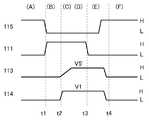
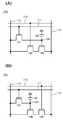
도 13의 (A)에 반도체 장치(130)를 나타낸다. 반도체 장치(130)는 트랜지스터(101), 트랜지스터(102), 용량 소자(103), 트랜지스터(107)를 포함한다.FIG. 13A shows a
반도체 장치(130)는 반도체 장치(100)(도 1)와 비교하면, 트랜지스터(107)가 포함되고, 용량 소자(103)의 다른 한쪽의 전극에 기준 전위 단자보다 기준 전위(GND)가 인가되어 있는 점이 다르다. 단, 용량 소자(103)의 다른 한쪽의 전극에는, 기준 전위는 아니고, 전원 전위 단자보다 전원 전위(VSS)나 그 외의 전위가 인가되어 있어도 좋다.The
트랜지스터(107)는 p형의 트랜지스터이다. 트랜지스터(107)의 채널이 형성되는 영역은 산화물 반도체, 실리콘 등 다양한 재료를 포함하는 층을 이용할 수 있다.The
트랜지스터(107)의 게이트는 배선(115)에 전기적으로 접속된다. 배선(115)은 워드선으로서 기능할 수 있다.The gate of the
트랜지스터(107)의 소스 및 드레인의 한쪽은 트랜지스터(102)의 소스 및 드레인의 다른 한쪽에 전기적으로 접속된다.One of the source and the drain of the
트랜지스터(107)의 소스 및 드레인의 다른 한쪽은 배선(113)에 전기적으로 접속된다. 트랜지스터(107)의 소스 및 드레인의 다른 한쪽은 트랜지스터(101)의 소스 및 드레인의 한쪽에 전기적으로 접속된다.The other of the source and the drain of the
단, 반도체 장치(135)와 같이, 트랜지스터(107)는 트랜지스터(102)와 배선(114)의 사이에 제공해도 좋다(도 13의 (B)). 반도체 장치(135)에서는, 트랜지스터(107)의 소스 및 드레인의 한쪽은 배선(114)에 전기적으로 접속되고, 소스 및 드레인의 다른 한쪽은 트랜지스터(102)의 소스 및 드레인의 한쪽에 전기적으로 접속된다.However, like the
트랜지스터(102)의 소스 및 드레인의 다른 한쪽은 배선(113)에 전기적으로 접속된다. 트랜지스터(102)의 소스 및 드레인의 다른 한쪽은 트랜지스터(101)의 소스 및 드레인의 한쪽에 전기적으로 접속된다.The other of the source and the drain of the
반도체 장치(130)에 대한 데이터의 기록 동작 및 반도체 장치(130)로부터의 데이터의 판독 동작을 설명한다.The operation of writing data to the
(기록 동작)(Write operation)
우선 기록 동작의 일례를 설명한다. 도 14에 타이밍 차트를 나타낸다. 도 15의 (A) 내지 도 15의 (E)에 반도체 장치(130)의 동작을 나타낸다. 일례로서 판독하고자 하는 전압을 V1으로 하고, 노드(104)의 전위(트랜지스터(102)의 게이트 전위)를 V5까지 변화시킴으로써 기록하는 동작을 설명한다. 멀티 비트 데이터를 저장할 때에는 다양한 전압을 인가할 필요가 있기 때문에, V1을 자유롭게 설정할 수 있는 점에서 유익하다.First, an example of the recording operation will be described. 14 is a timing chart. Figs. 15A to 15E show the operation of the
데이터를 기록하는 동작은 제1 스텝 및 제2 스텝에 의해 행해진다. 제1 스텝에서, 배선(113) 및 배선(114)에 저전압을 인가하고, 배선(111)에 고전압을 인가하여 트랜지스터(101)를 온으로 하고, 트랜지스터(102)가 온이 되고, 또한 배선(115)에 저전압을 인가하고 트랜지스터(107)를 온으로 한다. 제2 스텝에서, 배선(114)에 전압(V1)을 인가하고, 또한 배선(113)에 대한 저전압의 인가를 차단한다.An operation of recording data is performed by a first step and a second step. In the first step, a low voltage is applied to the
제2 스텝에 의해, 배선(114)으로부터, 트랜지스터(102)의 소스 및 드레인, 트랜지스터(107)의 소스 및 드레인, 배선(113), 및 트랜지스터(101)의 소스 및 드레인을 통하여, 노드(104)에 데이터(전압(V1))에 따른 전위(V5)가 인가된다. 그리고 트랜지스터(102)의 게이트에 V5가 인가된다. 용량 소자(103)에는 V5에 따른 전하가 축적된다.Through the
도 15(A)에 반도체 장치(130)의 초기 상태를 나타낸다. 도 14에서는 초기 상태를 (A)로 나타낸다.Fig. 15A shows an initial state of the
배선(111)에 저전압의 신호가 입력되고, 트랜지스터(101)는 오프한다.A low-voltage signal is input to the
배선(115)에 고전압의 신호가 입력되고, 트랜지스터(107)는 오프한다.A high-voltage signal is input to the
용량 소자(103)의 다른 한쪽의 전극에는 기준 전위 등의 저전압이 인가된다. 노드(104)에는 용량 소자(103)의 용량치에 대응한 전압이 인가된다.A low voltage such as a reference potential is applied to the other electrode of the
배선(113) 및 배선(114)에 저전압(GND)이 인가된다. 이것에 의해 배선(113) 및 배선(114)에 저전압을 프리차지할 수 있다. 여기에서는 저전압은 기준 전압(GND)으로 하고 있지만, 전원 전압(VSS)이나 그 외의 전압이어도 좋다.A low voltage (GND) is applied to the
도 15의 (B)에 기록 전의 준비 상태를 나타낸다. 도 14에서는 상기 상태를 (B)로 나타낸다.FIG. 15 (B) shows the ready state before writing. In Fig. 14, this state is indicated by (B).
시각 t1에서 배선(111)에 고전압의 신호가 입력된다. 트랜지스터(101)는 온한다.At time t1, a high-voltage signal is input to the
트랜지스터(101)가 온함으로써, 배선(113)과 노드(104)는 전기적으로 접속된다. 배선(113)의 전위가 노드(104)에 인가되고 그 결과, 트랜지스터(102)는 온한다.When the
시각 t1에서 배선(115)에 저전압의 신호가 입력된다. 트랜지스터(107)는 온한다. 상기 저전압은 트랜지스터(107)를 온할 수 있는 전압이면 좋다. 상기 저전압은 기준 전압(GND), 전원 전압(VSS)이나 그 외의 전압이어도 좋다.At time t1, a low-voltage signal is input to the
배선(113) 및 배선(114)에 저전압이 인가되고, 트랜지스터(101), 트랜지스터(102), 및 트랜지스터(107)가 온한다. 제1 스텝이 종료된다.A low voltage is applied to the
도 15의 (C), 도 15의 (D)에 기록 시의 상태를 나타낸다. 도 14에서는 상기 상태를 (C), (D)로 나타낸다.15 (C) and 15 (D) show the state at the time of recording. In Fig. 14, the states are indicated by (C) and (D).
시각 t2에서 배선(114)에, 전압(V1)을 인가한다(도 15의 (C)). 전압(V1)은 판독 동작 시에 판독하고자 하는 전압이다. V1의 크기는 기록하고자 하는 데이터에 맞추어 자유롭게 설정할 수 있다.At time t2, the voltage V1 is applied to the wiring 114 (Fig. 15 (C)). Voltage V1 is the voltage to be read in the read operation. The size of V1 can be freely set according to the data to be recorded.
시각 t2에서 배선(113)으로의 저전압(GND)의 공급을 차단한다(도 15의 (C)). 이 때, 배선(113)은 프리차지된 전압으로부터, 전기적으로 부유 상태가 된다. 즉, 배선(113)은 전하의 충전 또는 방전에 의해 전위의 변동이 용이하게 발생하는 상태가 된다. 이 부유 상태는 배선(113)에 전위를 공급하는 스위치를 오프함으로써 실현할 수 있다.At time t2, the supply of the low voltage (GND) to the
트랜지스터(107) 및 트랜지스터(102)가 온하고 있기 때문에, 배선(113)은 배선(114)과 전기적으로 접속된다. 배선(113)의 전압은 프리차지된 저전압(GND)으로부터 V5'까지 변화한다(도 15의 (D)). 단, V5'는 V1과 대략 트랜지스터(102) 및 트랜지스터(107)의 문턱 전압만큼 다르다(V1>V5').The
트랜지스터(101)가 온하고 있기 때문에, 배선(114)으로부터, 트랜지스터(102)의 소스 및 드레인, 트랜지스터(107)의 소스 및 드레인, 배선(113), 및 트랜지스터(101)의 소스 및 드레인을 통하여, 노드(104)(트랜지스터(102)의 게이트)에 데이터가 기록된다. 용량 소자(103)에 전하가 축적된다. 노드(104)의 전위는 V5까지 변화한다.The source and drain of the
노드(104)의 전위가 V5까지 변화하면, 트랜지스터(102)의 게이트와 소스 사이의 전위차가 작아져; 트랜지스터(102)의 소스와 드레인 사이를 흐르는 전류(Id)는 작아진다. 최종적으로 트랜지스터(102)는 오프한다.When the potential of the
반도체 장치(130)에서는, 배선(114)에는 V1이 인가되고, 배선(113)에는 V5'가 인가되고, 노드(104)에는 V5가 인가된 상태가 된다.In the
배선(114)에 전압(V1)이 인가되고, 또한 배선(113)에 대한 저전압의 인가가 차단되어, 제2 스텝이 종료된다.The voltage V1 is applied to the
이상에 의해, 판독하고자 하는 전압(V1)을 배선(114)에 인가하고, 노드(104)의 전위를 V5까지 변화시킴으로써, 기록하는 동작이 종료된다.As described above, the writing operation is ended by applying the voltage V1 to be read to the
도 15의 (E)에 기록 후, 유지 전의 상태를 나타낸다. 도 14에서는 상기 상태를 (E)로 나타낸다.15 (E) shows the state before the holding. In Fig. 14, this state is indicated by (E).
시각 t3에서 배선(111)에 저전압의 신호가 입력된다. 트랜지스터(101)는 오프한다. 노드(104)는 배선(113)과 전기적으로 접속되지 않는 상태가 된다. 트랜지스터(101)는 오프 전류가 매우 낮다는 특성을 가지기 때문에, 노드(104)의 전위(V5)는 유지된다.At time t3, a low-voltage signal is input to the
시각 t4까지의 동안에, 배선(115)에 고전압이 인가되고, 배선(113)에 저전압(GND)이 인가되고, 배선(114)에 저전압(GND)이 인가된다.A high voltage is applied to the
배선(115)에 고전압이 인가되면, 트랜지스터(107)는 오프한다. 상기 고전압은 트랜지스터(107)를 오프할 수 있는 전압이면 좋다.When a high voltage is applied to the
시각 t4에는 유지 상태가 된다. 도 14에서는 상기 상태를 (F)로 나타낸다. 반도체 장치(130)는 노드(104)의 전위(V5)를 제외하고, 도 15의 (A)와 같은 상태가 된다. 트랜지스터(101) 및 트랜지스터(107)는 오프한다.At time t4, the holding state is established. In Fig. 14, this state is indicated by (F). The
단, 도 14의 (A), 도 14의 (F) 상태에서는, 배선(114)에 저전압을 인가하고 있지만, 고전압을 인가해도 좋다. 배선(114)에 고전압을 인가해 두면, (E) 상태로부터 (F) 상태, 즉 배선(114)에 고전압을 인가할 때에, 신속하게 전압을 변화시킬 수 있는 경우가 있다.14 (A) and 14 (F), although the low voltage is applied to the
(판독 동작)(Read operation)
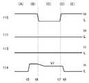
다음에, 상기 기록 동작에 의해, 기록된 전하로부터, 전압(V1)을 판독하는 동작의 일례를 설명한다. 도 16에 타이밍 차트를 나타낸다. 도 17의 (A) 내지 도 17의 (D)에 반도체 장치(130)의 동작을 나타낸다.Next, an example of an operation of reading the voltage V1 from the recorded electric charges by the above-described writing operation will be described. Fig. 16 shows a timing chart. Figs. 17A to 17D show the operation of the
데이터를 판독하는 동작은 배선(114)에 고전압을 인가하는 제3 스텝, 배선(114)에 대한 고전압의 인가를 차단하고, 배선(115)에 저전압을 인가하여 트랜지스터(107)를 온으로 하는 제4 스텝에 의해 행해진다. 제4 스텝에 의해, 배선(114)의 전압은 고전압으로부터 전압(V1)으로 변화한다.A third step of applying a high voltage to the
도 17의 (A)에 반도체 장치(130)의 유지 상태를 나타낸다. 도 16에서는 유지 상태를 (A)로 나타낸다.Fig. 17A shows the holding state of the
도 17의 (B)에 판독하기 전의 준비 상태를 나타낸다. 도 16에서는 상기 상태를 (B)로 나타낸다.Fig. 17 (B) shows the ready state before reading. In Fig. 16, this state is indicated by (B).
시각 t5에서 배선(114)에 고전압(VDD)이 인가된다. 배선(114)에 고전압을 프리차지할 수 있다.At time t5, the high voltage VDD is applied to the
단, 트랜지스터(101) 및 트랜지스터(107)는 유지 상태로부터 오프한 상태이다.However, the
배선(114)에 고전압이 인가되어, 제3 스텝이 종료된다.A high voltage is applied to the
도 17의 (C), 도 17의 (D)에 판독 시의 상태를 나타낸다. 도 16에서는 상기 상태를 (C)로 나타낸다.17 (C) and 17 (D) show the state at the time of reading. In Fig. 16, this state is indicated by (C).
시각 t6에서 배선(114)으로의 고전압(VDD)의 공급을 차단한다(도 17의 (C)). 이 때, 배선(114)은 프리차지된 전압으로부터 전기적으로 부유 상태가 된다. 즉, 배선(114)은 전하의 충전 또는 방전에 의해 전위의 변동이 용이하게 발생하는 상태가 된다. 이 부유 상태는 배선(114)에 전위를 공급하는 스위치를 오프함으로써 실현할 수 있다.At time t6, supply of the high voltage VDD to the
시각 t6에서 배선(115)에 저전압의 신호가 입력된다. 트랜지스터(107)는 온한다.At time t6, a low-voltage signal is input to the
트랜지스터(102)의 게이트에는 전압(V5)이 인가된다. 트랜지스터(102)는 온한다. 배선(114)의 전위는 게이트 전압(V5)에 대응하여, 프리차지된 고전압(VDD)으로부터 전압(V1)까지 변화한다(도 17의 (D)). 트랜지스터(102)의 게이트와 소스 사이의 전위차는 시간 경과와 함께 작아지고, 최종적으로는 트랜지스터(102)는 오프한다.A voltage V5 is applied to the gate of the
배선(114)을 판별 회로 등에 전기적으로 접속시켜 V1을 판독한다. 이것에 의해 전압(V1)을 판독할 수 있다.The
배선(114)에의 고전압의 인가가 차단되고, 트랜지스터(107)가 온한다. 따라서, 제4 스텝이 종료된다.The application of the high voltage to the
판독 후에는 시각 t7에서 배선(115)에 고전압의 신호가 입력된다. 트랜지스터(107)는 오프한다(도 16의 (D)).After reading, a high-voltage signal is input to the
시각 t8까지의 동안에, 배선(114)에 저전압(GND)이 인가된다(도 16의(D)).During time t8, a low voltage GND is applied to the wiring 114 (Fig. 16 (D)).
시각 t8에는 유지 상태가 된다. 도 16에서는 상기 상태를 (E)로 나타낸다. 반도체 장치(130)는 도 17의 (A)와 같은 상태가 된다.At time t8, the holding state is established. In Fig. 16, this state is indicated by (E). The
단, 도 16의 (A), 도 16의 (E) 상태에서는 배선(114)에 저전압을 인가하고 있지만, 고전압을 인가해도 좋다. 배선(114)에 고전압을 인가해 두면, (A) 상태로부터 (B) 상태, 즉 배선(114)에 VDD를 인가할 때, 신속하게 전압을 변화시킬 수 있다.16 (A) and 16 (E), although a low voltage is applied to the
단, 노드(104)의 전위, 즉 트랜지스터(102)의 게이트에 인가된 전압을 리셋하는 경우는, 예를 들면 배선(111)에 고전압의 신호를 입력하여 트랜지스터(101)를 온으로 한다. 따라서, 트랜지스터(101)가 온이 되면, 노드(104)는 배선(113)과 전기적으로 접속된다. 배선(113)에는 GND가 인가되어 있기 때문에, 노드(104)의 전위는 리셋된다.However, in the case of resetting the potential of the
반도체 장치(130)에서는, 기록 시에 배선(114)에 인가한 전위(V1)가 그대로 판독 전위가 된다.In the
반도체 장치(130)는 반도체 장치(100)와 마찬가지로, 실시형태 1에 나타낸 효과를 나타낼 수 있다. 또한, 반도체 장치(130)에서의 트랜지스터(107)가 전기적으로 접속된 배선(115)의 용량은 반도체 장치(100)에서의 용량 소자(103)가 전기적으로 접속된 배선(112)의 용량보다 작게 할 수 있으므로; 반도체 장치(130)에서는 보다 소비 전력을 작게 할 수 있게 된다.The
또한, 도 13의 (B)에 나타내는 반도체 장치(135)의 동작은 반도체 장치(130)와 같기 때문에; 반도체 장치(130)의 동작의 기재를 원용한다.Since the operation of the
본 실시형태는 다른 실시형태의 기재와 적절히 조합할 수 있다.This embodiment mode can be appropriately combined with the description of another embodiment mode.
(실시형태 4)(Fourth Embodiment)
도 18에 반도체 장치(140)를 나타낸다. 반도체 장치(140)는 트랜지스터(101), 트랜지스터(106), 용량 소자(103)를 포함한다.Fig. 18 shows a
반도체 장치(140)는 반도체 장치(100)(도 1)와 비교하면, 트랜지스터(106)가 n형 트랜지스터인 점이 다르다.The
트랜지스터(106)의 채널이 형성되는 영역에 산화물 반도체, 실리콘 등 다양한 재료를 포함하는 층을 이용할 수 있다.A layer including various materials such as an oxide semiconductor and silicon may be used in the region where the channel of the
트랜지스터(106)와 트랜지스터(101) 등의 다른 소자와의 접속에 대해서는, 트랜지스터(102)와 트랜지스터(101) 등의 다른 소자와의 접속의 기재를 원용한다.The description of the connection between the
반도체 장치(140)로의 데이터의 기록 동작 및 반도체 장치(140)로부터의 데이터의 판독 동작을 설명한다.The operation of writing data into the
(기록 동작)(Write operation)
우선 기록 동작의 일례를 설명한다. 도 19에 타이밍 차트를 나타낸다. 도 20의 (A) 내지 도 20의 (E)에 반도체 장치(140)의 동작을 나타낸다. 일례로서 판독하고자 하는 전압을 V1으로 하고, 노드(104)의 전위(트랜지스터(106)의 게이트 전위)를 V7까지 변화시킴으로써, 데이터를 기록하는 동작을 설명한다. 멀티 비트 데이터를 저장할 때에는 다양한 전압을 인가할 필요가 있기 때문에, V1을 자유롭게 설정할 수 있는 점에서 유익하다.First, an example of the recording operation will be described. Fig. 19 shows a timing chart. Figs. 20A to 20E show the operation of the
데이터를 기록하는 동작은 제1 스텝 및 제2 스텝에 의해 행해진다. 제1 스텝에서, 배선(113) 및 배선(114)에 고전압을 인가하고, 배선(111)에 고전압을 인가하여 트랜지스터(101)를 온으로 하고, 한쪽 배선(112)에 고전압을 인가하여 트랜지스터(106)를 온으로 한다. 제2 스텝에서, 배선(114)에 전압(V1)을 인가하고, 한쪽 배선(113)에 대한 고전압의 인가를 차단한다.An operation of recording data is performed by a first step and a second step. In the first step, a high voltage is applied to the
제2 스텝에 의해, 배선(114)으로부터, 트랜지스터(106)의 소스 및 드레인, 배선(113), 및 트랜지스터(101)의 소스 및 드레인을 통하여, 노드(104)에 데이터(전압(V1))에 따른 전위(V7)가 인가된다. 그리고 트랜지스터(106)의 게이트에 V7이 인가된다. 용량 소자(103)에는 V7에 따른 전하가 축적된다.The data (voltage V1) is supplied to the
도 20의 (A)에 반도체 장치(140)의 초기 상태를 나타낸다. 도 19에서는 초기 상태를 (A)로 나타낸다.FIG. 20A shows the initial state of the
배선(111)에 저전압의 신호가 입력되고, 트랜지스터(101)는 오프한다.A low-voltage signal is input to the
배선(112)에는 저전압의 신호가 입력된다. 노드(104)에는 용량 소자(103)의 용량치에 대응한 전압이 인가된다.A signal of a low voltage is input to the
배선(113) 및 배선(114)에 고전압(VDD)이 인가된다. 이것에 의해 배선(113) 및 배선(114)에 고전압을 프리차지할 수 있다. 여기에서는 고전압은 전원 전압(VDD)으로 하고 있지만, 그 외의 전압이어도 좋다.The high voltage VDD is applied to the
도 20의 (B)에 기록 전의 준비 상태를 나타낸다. 도 19에서는 상기 상태를 (B)로 나타낸다.FIG. 20 (B) shows the ready state before writing. In Fig. 19, this state is indicated by (B).
시각 t1에서 배선(111)에 고전압의 신호가 입력되고, 따라서 트랜지스터(101)는 온한다.At time t1, a high-voltage signal is input to the
트랜지스터(101)가 온함으로써, 배선(113)과 노드(104)는 전기적으로 접속된다. 노드(104)의 전위는 상승하여 고전압(VDD)이 된다.When the
시각 t1에서 배선(112)에 고전압의 신호가 입력된다. 노드(104)에는 용량 소자(103)의 용량치에 대응한 전압이 인가된다. 트랜지스터(101)가 온하고, 또한 배선(112)에 고전압이 인가되어, 트랜지스터(106)는 온한다. 상기 고전압은 트랜지스터(106)를 온할 수 있는 전압이면 좋고, 전원 전압(VDD)이나 그 외의 전압이어도 좋다.At time t1, a high-voltage signal is input to the
배선(113) 및 배선(114)에 고전압이 인가되어, 트랜지스터(101) 및 트랜지스터(106)가 온 한다. 제1 스텝이 종료된다.A high voltage is applied to the
도 20의 (C), 도 20의 (D)에 기록 시의 상태를 나타낸다. 도 19에서는 상기 상태를 (C), (D)로 나타낸다.20 (C) and 20 (D) show the state at the time of recording. In Fig. 19, the above states are indicated by (C) and (D).
시각 t2에서 배선(114)에, 전압(V1)을 인가한다(도 20의 (C)). 전압(V1)은 판독 동작 시에 판독하고자 하는 전압이다. V1의 크기는 기록하고자 하는 데이터에 맞추어 자유롭게 설정할 수 있다.At time t2, the voltage V1 is applied to the wiring 114 (Fig. 20 (C)). Voltage V1 is the voltage to be read in the read operation. The size of V1 can be freely set according to the data to be recorded.
시각 t2에서 배선(113)으로의 고전압(VDD)의 공급을 차단한다(도 20의 (C)). 이 때, 배선(113)은 프리차지된 전압으로부터, 전기적으로 부유 상태가 된다. 즉, 배선(113)은 전하의 충전 또는 방전에 의해 전위의 변동이 용이하게 발생하는 상태가 된다. 이 부유 상태는 배선(113)에 전위를 공급하는 스위치를 오프함으로써 실현할 수 있다.At time t2, supply of the high voltage VDD to the
트랜지스터(106)가 온하고 있기 때문에, 배선(113)은 배선(114)과 전기적으로 접속된다. 배선(113)의 전압은 프리차지된 고전압(VDD)으로부터 V7'까지 변화한다(도 20의 (D)). 단, V7'는 V1과 대략 트랜지스터(106)의 문턱 전압만큼 다르다.Since the
트랜지스터(101)가 온하고 있기 때문에, 배선(114)으로부터, 트랜지스터(106)의 소스 및 드레인, 배선(113), 및 트랜지스터(101)의 소스 및 드레인을 통하여, 노드(104)(트랜지스터(106)의 게이트)에 데이터가 기록된다. 용량 소자(103)에 전하가 축적된다. 그리고 노드(104)의 전위는 V7까지 변화한다.The
노드(104)의 전위가 V7까지 변화하면, 트랜지스터(106)의 게이트와 소스 사이의 전위차가 작아져; 트랜지스터(106)의 소스와 드레인 사이를 흐르는 전류(Id)는 낮아진다. 최종적으로는 트랜지스터(106)는 오프한다.When the potential of the
반도체 장치(140)에서는, 배선(114)에는 V1이 인가되고, 배선(113)에는 V7'가 인가되고, 노드(104)에는 V7이 인가된 상태가 된다.In the
배선(114)에 전압(V1)이 인가되고, 또한 배선(113)에 대한 고전압의 인가가 차단되어, 제2 스텝이 종료된다.The voltage V1 is applied to the
이상에 의해, 판독하고자 하는 전압(V1)을 배선(114)에 인가하여, 노드(104)의 전위를 V7까지 변화시킴으로써 기록 동작이 종료된다.Thus, the writing operation is ended by applying the voltage V1 to be read to the
도 20의 (E)에 기록 후, 유지 전의 상태를 나타낸다. 도 19에서는 상기 상태를 (E)로 나타낸다.FIG. 20 (E) shows the state before recording, after recording. In Fig. 19, this state is shown by (E).
시각 t3에서 배선(111)에 저전압의 신호가 입력된다. 트랜지스터(101)는 오프한다. 노드(104)는 배선(113)과 전기적으로 접속되지 않는 상태가 된다. 트랜지스터(101)는 오프 전류가 매우 낮다는 특성을 가지기 때문에, 노드(104)의 전위(V7)는 유지된다.At time t3, a low-voltage signal is input to the
시각 t4까지의 동안에, 배선(112)에 저전압이 인가되고, 배선(113)에 고전압(VDD)이 인가되고, 배선(114)에 고전압(VDD)이 인가된다.A low voltage is applied to the
배선(112)에 저전압이 인가되면, 노드(104)의 전위는 V7로부터 트랜지스터(106)를 오프할 수 있는 전압까지 변화한다.When a low voltage is applied to the
시각 t4에는 유지 상태가 된다. 도 19에서는 상기 상태를 (F)로 나타낸다. 반도체 장치(140)는 노드(104)의 전위가 다른 점을 제외하고, 도 20의 (A)와 같은 상태가 된다. 트랜지스터(101)는 오프한다.At time t4, the holding state is established. In Fig. 19, this state is indicated by (F). The
단, 도 19의 (A), 도 19의 (F) 상태에서는, 배선(114)에 고전압을 인가하고 있지만, 저전압을 인가해도 좋다. 배선(114)에 저전압을 인가해 두면, (E) 상태로부터 (F) 상태, 즉 배선(114)에 저전압을 인가할 때에, 신속하게 전압을 변화시킬 수 있는 경우가 있다.19 (A) and 19 (F), although a high voltage is applied to the
(판독 동작)(Read operation)
다음에, 상기 기록 동작에 의해, 기록된 전하로부터 전압(V1)을 판독하는 동작의 일례를 설명한다. 도 21에 타이밍 차트를 나타낸다. 도 22의 (A) 내지 도 22의 (D)에 반도체 장치(140)의 동작을 나타낸다.Next, an example of an operation of reading the voltage V1 from the recorded charge by the above-described recording operation will be described. 21 is a timing chart. Figs. 22A to 22D show the operation of the
데이터를 판독하는 동작은 배선(114)에 저전압을 인가하는 제3 스텝, 배선(114)에 대한 저전압의 인가를 차단하고, 또한 배선(112)에 고전압을 인가하는 제4 스텝에 의해 행해진다. 제4 스텝에 의해, 배선(114)의 전압은 저전압으로부터 전압(V1)으로 변화한다.The data reading operation is performed in a third step of applying a low voltage to the
도 22의 (A)에 반도체 장치(140)의 유지 상태를 나타낸다. 도 21에서는 유지 상태를 (A)로 나타낸다.22 (A) shows the holding state of the
도 22의 (B)에 판독하기 전의 준비 상태를 나타낸다. 도 21에서는 상기 상태를 (B)로 나타낸다.22 (B) shows the ready state before reading. In Fig. 21, this state is indicated by (B).
시각 t5에서 배선(114)에 저전압(GND)이 인가된다. 배선(114)에 저전압을 프리차지할 수 있다. 여기에서는 배선(114)에는 GND를 인가하고 있다. 하지만, 전원 전압(VSS)이나 그 외의 전압을 인가해도 좋다.At time t5, a low voltage (GND) is applied to the
단, 트랜지스터(101) 및 트랜지스터(106)는 유지 상태로부터 오프한 상태이다.However, the
배선(114)에 저전압이 인가되어, 제3 스텝이 종료된다.A low voltage is applied to the
도 22의 (C), 도 22의 (D)에 판독 시의 상태를 나타낸다. 도 21에서는 상기 상태를 (C)로 나타낸다.Figures 22 (C) and 22 (D) show states at the time of reading. In Fig. 21, this state is indicated by (C).
시각 t6에서 배선(114)으로의 저전압(GND)의 공급을 차단한다(도 22의 (C)). 이 때, 배선(114)은 프리차지된 전압으로부터 전기적으로 부유 상태가 된다. 즉, 배선(114)은 전하의 충전 또는 방전에 의해 전위의 변동이 용이하게 발생하는 상태가 된다. 이 부유 상태는 배선(114)에 전위를 공급하는 스위치를 오프함으로써 실현할 수 있다.At time t6, the supply of the low voltage (GND) to the
시각 t6에서 배선(112)에 고전압의 신호가 입력된다. 노드(104)의 전위는 기록 시의 V7까지 변화한다. 그 결과, 트랜지스터(106)의 게이트 전위(V7)와 배선(114)의 전위에 대응한 전류(Id)가 흐른다. 단, 배선(112)에 입력되는 고전압은 기록 동작 시에 배선(112)에 입력된 고전압과 같은 전압인 것이 바람직하다.At time t6, a high-voltage signal is input to the
배선(114)의 전위는 게이트 전압(V7)에 대응하여, 프리차지된 저전압(GND)으로부터 V1까지 변화한다(도 22의 (D)). 트랜지스터(106)의 게이트와 소스 사이의 전위차는 시간 경과와 함께 작아지고, 최종적으로는 트랜지스터(106)는 오프한다.The potential of the
배선(114)을 판별 회로 등에 전기적으로 접속시켜 V1을 판독한다. 이것에 의해 전압(V1)을 판독할 수 있다.The
배선(114)에의 저전압의 인가가 차단되고, 배선(112)에 고전압이 인가된다. 따라서, 제4 스텝이 종료된다.The application of the low voltage to the
판독 후, 시각 t7에서 배선(112)에 저전압의 신호가 입력된다. 배선(112)에 저전압이 인가되면, 노드(104)의 전위는 V7로부터 상기 저전압만큼 변화한다. 따라서, 트랜지스터(106)는 오프한다.After reading, a low-voltage signal is input to the
시각 t4까지의 동안에, 배선(114)에 고전압(VDD)이 인가된다.During time t4, the high voltage VDD is applied to the
시각 t8에는 유지 상태가 된다. 도 21에서는 상기 상태를 (E)로 나타낸다. 반도체 장치(140)는 도 22의 (A)와 같은 상태가 된다.At time t8, the holding state is established. In Fig. 21, this state is indicated by (E). The
단, 도 21의 (A), 도 21의 (E) 상태에서는 배선(114)에 고전압을 인가하고 있지만, 저전압을 인가해도 좋다. 배선(114)에 저전압을 인가해 두면, (A) 상태로부터 (B) 상태, 즉 배선(114)에 GND를 인가할 때에, 신속하게 전압을 변화시킬 수 있다.21 (A) and 21 (E), although a high voltage is applied to the
단, 노드(104)의 전위, 즉 트랜지스터(106)의 게이트에 인가된 전위를 리셋하는 경우는, 예를 들면 배선(112)에 고전압을 인가하고, 또한 배선(113)에 GND 등의 저전압을 인가하고, 배선(111)에 고전압의 신호를 입력하여 트랜지스터(101)를 온으로 한다. 트랜지스터(101)가 온이 되면, 노드(104)는 배선(113)과 전기적으로 접속된다. 배선(113)에는 GND이 인가되기 때문에, 노드(104)의 전위는 리셋 소거된다.When resetting the potential of the
반도체 장치(140)는 기록 시에 배선(114)에 인가한 전위(V1)가 그대로 판독 전위가 된다.In the
반도체 장치(140)는 반도체 장치(100)와 마찬가지로, 실시형태 1에 나타낸 효과를 얻을 수 있다.The
본 실시형태는 다른 실시형태의 기재와 적절히 조합할 수 있다.This embodiment mode can be appropriately combined with the description of another embodiment mode.
(실시형태 5)(Embodiment 5)
도 23의 (A)에 반도체 장치(150)를 나타낸다. 반도체 장치(150)는 트랜지스터(101), 트랜지스터(106), 용량 소자(103), 트랜지스터(108)를 포함한다.23 (A) shows a
반도체 장치(150)는 반도체 장치(100)(도 1)와 비교하면, 트랜지스터(102) 대신에 트랜지스터(106)를 포함한다. 반도체 장치(150)는 트랜지스터(108)를 포함하고, 용량 소자(103)의 다른 한쪽의 전극에 기준 전위 단자보다 기준 전위(GND)가 인가된다. 단, 용량 소자(103)의 다른 한쪽의 전극에는, 기준 전위는 아니고, 전원 전위 단자보다 전원 전위(VSS)나 그 외의 전위가 인가되어도 좋다.The
트랜지스터(102) 대신에 제공된 트랜지스터(106)는 n형의 트랜지스터이다. 트랜지스터(106)의 채널이 형성되는 영역은 산화물 반도체, 실리콘 등 다양한 재료를 포함하는 층을 이용할 수 있다.The
트랜지스터(106)와 트랜지스터(101) 등의 다른 소자와의 접속에 대해서는, 트랜지스터(102)와 트랜지스터(101) 등의 다른 소자와의 접속의 기재를 원용한다.The description of the connection between the
트랜지스터(108)는 n형의 트랜지스터이다. 트랜지스터(108)의 채널이 형성되는 영역은 산화물 반도체, 실리콘 등 다양한 재료를 포함하는 층을 이용할 수 있다.
트랜지스터(108)의 게이트는 배선(115)에 전기적으로 접속된다. 배선(115)은 워드선으로서 기능할 수 있다.The gate of the
트랜지스터(108)의 소스 및 드레인의 한쪽은 트랜지스터(106)의 소스 및 드레인의 다른 한쪽에 전기적으로 접속된다.One of the source and the drain of the
트랜지스터(108)의 소스 및 드레인의 다른 한쪽은 배선(113)에 전기적으로 접속된다. 트랜지스터(108)의 소스 및 드레인의 다른 한쪽은 트랜지스터(101)의 소스 및 드레인의 한쪽에 전기적으로 접속된다.The other of the source and the drain of the
단, 반도체 장치(155)와 같이, 트랜지스터(108)는 트랜지스터(106)와 배선(114)의 사이에 제공해도 좋다(도 23의 (B)). 반도체 장치(155)에서는, 트랜지스터(108)의 소스 및 드레인의 한쪽은, 배선(114)에 전기적으로 접속되고, 소스 및 드레인의 다른 한쪽은 트랜지스터(106)의 소스 및 드레인의 한쪽에 전기적으로 접속된다.However, like the
트랜지스터(106)의 소스 및 드레인의 다른 한쪽은 배선(113)에 전기적으로 접속된다. 트랜지스터(106)의 소스 및 드레인의 다른 한쪽은 트랜지스터(101)의 소스 및 드레인의 한쪽에 전기적으로 접속된다.The other of the source and the drain of the
반도체 장치(150)로의 데이터의 기록 동작 및 반도체 장치(150)로부터의 데이터의 판독 동작을 설명한다.The operation of writing data into the
(기록 동작)(Write operation)
우선 기록 동작의 일례를 설명한다. 도 24에 타이밍 차트를 나타낸다. 도 25의 (A) 내지 도 25의 (E)에 반도체 장치(150)의 동작을 나타낸다. 일례로서 판독하고자 하는 전압을 V1으로 하고, 노드(104)의 전위(트랜지스터(106)의 게이트 전위)를 V9까지 변화시킴으로써 기록하는 동작을 설명한다. 멀티 비트 데이터를 저장할 때에는 다양한 전압을 인가할 필요가 있기 때문에, V1을 자유롭게 설정할 수 있는 점에서 유익하다.First, an example of the recording operation will be described. 24 is a timing chart. Figs. 25A to 25E show the operation of the
데이터를 기록하는 동작은, 제1 스텝 및 제2 스텝에 의해 행해진다. 제1 스텝에서, 배선(113) 및 배선(114)에 고전압을 인가하고, 배선(111)에 고전압을 인가하여 트랜지스터(101)를 온으로 하고, 트랜지스터(106)가 온이 되고, 또한 배선(115)에 고전압을 인가하여 트랜지스터(108)를 온으로 한다. 제2 스텝에서, 배선(114)에 전압(V1)을 인가하고, 또한 배선(113)에 대한 고전압의 인가를 차단한다.The operation of writing data is performed by the first step and the second step. In the first step, a high voltage is applied to the
제2 스텝에 의해, 배선(114)으로부터, 트랜지스터(106)의 소스 및 드레인, 트랜지스터(108)의 소스 및 드레인, 배선(113), 및 트랜지스터(101)의 소스 및 드레인을 통하여, 노드(104)에 데이터(전압(V1))에 따른 전위(V9)가 인가된다. 그리고 트랜지스터(106)의 게이트에 V9가 인가된다. 용량 소자(103)에는 V9에 따른 전하가 축적된다.The source and drain of the
도 25의 (A)에 반도체 장치(150)의 초기 상태를 나타낸다. 도 24에서는 초기 상태를 (A)로 나타낸다.Fig. 25A shows the initial state of the
배선(111)에 저전압의 신호가 입력되어, 트랜지스터(101)는 오프한다.A signal of a low voltage is inputted to the
배선(115)에 저전압의 신호가 입력되어, 트랜지스터(108)는 오프한다. 상기 저전압은 트랜지스터(108)를 오프할 수 있는 전압이면 좋다. 상기 저전압은 기준 전위(GND), 전원 전압(VSS), 그 외의 전압이어도 좋다.A signal of a low voltage is input to the
용량 소자(103)의 다른 한쪽의 전극에는 기준 전위 등의 저전압이 인가된다. 노드(104)에는 용량 소자(103)의 용량치에 대응한 전압이 인가된다.A low voltage such as a reference potential is applied to the other electrode of the
배선(113) 및 배선(114)에 고전압(VDD)이 인가된다. 이것에 의해 배선(113) 및 배선(114)에 고전압을 프리차지할 수 있다. 여기에서는 고전압을 전원 전압(VDD)으로 하고 있지만, 그 외의 전압이어도 좋다.The high voltage VDD is applied to the
도 25의 (B)에 기록 전의 준비 상태를 나타낸다. 도 24에서는 상기 상태를 (B)로 나타낸다.Figure 25 (B) shows the ready state before writing. In Fig. 24, this state is indicated by (B).
시각 t1에서 배선(111)에 고전압의 신호가 입력되고, 따라서, 트랜지스터(101)는 온한다.At time t1, a high-voltage signal is input to the
트랜지스터(101)가 온함으로써, 배선(113)과 노드(104)와는 전기적으로 접속된다. 배선(113)의 전위가 노드(104)에 인가되고, 그 결과, 트랜지스터(106)는 온한다.As the
시각 t1에서 배선(115)에 고전압의 신호가 입력된다. 트랜지스터(108)는 온한다. 상기 고전압은 트랜지스터(108)를 온할 수 있는 전압이면 좋다. 상기 고전압은 전원 전압(VDD)이나 그 외의 전압이어도 좋다.At time t1, a high-voltage signal is input to the
배선(113) 및 배선(114)에 고전압이 인가되고, 트랜지스터(101), 트랜지스터(106) 및 트랜지스터(108)가 온한다. 제1 스텝이 종료된다.A high voltage is applied to the
도 25의 (C), 도 25의 (D)에 기록 시의 상태를 나타낸다. 도 24에서는 상기 상태를 (C), (D)로 나타낸다.25 (C) and 25 (D) show the state at the time of recording. In Fig. 24, the states are indicated by (C) and (D).
시각 t2에서 배선(114)에 전압(V1)을 인가한다(도 25의 (C)). 전압(V1)은 판독 동작 시에 판독하고자 하는 전압이다. V1의 크기는 기록하고자 하는 데이터에 맞추어 자유롭게 설정할 수 있다.At time t2, the voltage V1 is applied to the wiring 114 (Fig. 25 (C)). Voltage V1 is the voltage to be read in the read operation. The size of V1 can be freely set according to the data to be recorded.
시각 t2에서 배선(113)으로의 고전압(VDD)의 공급을 차단한다(도 25의 (C)). 이 때, 배선(113)은 프리차지된 전압으로부터, 전기적으로 부유 상태가 된다. 즉, 배선(113)은 전하의 충전 또는 방전에 의해 전위의 변동이 용이하게 발생하는 상태가 된다. 이 부유 상태는 배선(113)에 전위를 공급하는 스위치를 오프함으로써 실현될 수 있다.At time t2, supply of the high voltage VDD to the
트랜지스터(108) 및 트랜지스터(106)가 온하고 있음으로써, 배선(113)은 배선(114)과 전기적으로 접속된다. 배선(113)의 전압은 프리차지된 고전압(VDD)으로부터 V9'까지 변화한다(도 25의 (D)). 단, V9'는 V1과 대략 트랜지스터(106) 및 트랜지스터(108)의 문턱 전압만큼 다르다.Since the
트랜지스터(101)가 온하고 있음으로써, 배선(114)으로부터, 트랜지스터(106)의 소스 및 드레인, 트랜지스터(108)의 소스 및 드레인, 배선(113), 및 트랜지스터(101)의 소스 및 드레인을 통하여, 노드(104)(트랜지스터(106)의 게이트)에 데이터가 기록된다. 용량 소자(103)에 전하가 축적된다. 노드(104)의 전위는 V9까지 변화한다.The source and drain of the
노드(104)의 전위가 V9까지 변화하면, 트랜지스터(106)의 게이트와 소스 사이의 전위차가 작아지고; 그 결과 트랜지스터(106)의 소스와 드레인 사이를 흐르는 전류(Id)는 낮아진다. 그리고 최종적으로는 트랜지스터(106)는 오프한다.When the potential of the
반도체 장치(150)에서는, 배선(114)에는 V1이 인가되고, 배선(113)에는 V9'가 인가되고, 노드(104)에는 V9가 인가된 상태가 된다.In the
배선(114)에 전압(V1)이 인가되고, 또한 배선(113)에 대한 고전압의 인가가 차단되어, 제2 스텝이 종료된다.The voltage V1 is applied to the
이상에 의해, 판독하고자 하는 전압(V1)을 배선(114)에 인가하고, 노드(104)의 전위를 V9까지 변화시킴으로써 기록하는 동작이 종료된다.Thus, the writing operation is completed by applying the voltage V1 to be read to the
도 25의 (E)에 기록 후, 유지 전의 상태를 나타낸다. 도 24에서는 상기 상태를 (E)로 나타낸다.FIG. 25 (E) shows the state before the recording, after recording. In Fig. 24, this state is indicated by (E).
시각 t3에서 배선(111)에 저전압의 신호가 입력된다. 트랜지스터(101)는 오프한다. 노드(104)는 배선(113)과 전기적으로 접속되지 않는 상태가 된다. 트랜지스터(101)는 오프 전류가 매우 낮다는 특성을 가지기 때문에, 노드(104)의 전위(V9)는 유지된다.At time t3, a low-voltage signal is input to the
시각 t4까지의 동안에, 배선(115)에 저전압이 인가되고, 배선(113)에 고전압(VDD)이 인가되고, 배선(114)에 고전압(VDD)이 인가된다.A low voltage is applied to the
배선(115)에 저전압이 인가되면, 트랜지스터(108)는 오프한다. 상기 저전압은 트랜지스터(108)를 오프할 수 있는 전압이면 좋다.When a low voltage is applied to the
시각 t4에는 유지 상태가 된다. 도 24에서는 상기 상태를 (F)로 나타낸다. 반도체 장치(150)는 노드(104)의 전위(V9)를 제외하고, 도 25의 (A)와 같은 상태가 된다. 트랜지스터(101) 및 트랜지스터(108)는 오프한다.At time t4, the holding state is established. In Fig. 24, this state is indicated by (F). The
단, 도 24의 (A), 도 24의 (F) 상태에서는, 배선(114)에 고전압을 인가하고 있지만, 저전압을 인가해도 좋다. 배선(114)에 저전압을 인가해 두면, (E) 상태로부터 (F) 상태, 즉 배선(114)에 저전압을 인가할 경우에, 신속하게 전압을 변화시킬 수 있는 경우가 있다.24 (A) and 24 (F), although a high voltage is applied to the
(판독 동작)(Read operation)
다음에, 상기 기록 동작에 의해, 기록된 전하로부터 전압(V1)을 판독하는 동작의 일례를 설명한다. 도 26에 타이밍 차트를 나타낸다. 도 27의 (A) 내지 도 27의 (D)에 반도체 장치(150)의 동작을 나타낸다.Next, an example of an operation of reading the voltage V1 from the recorded charge by the above-described recording operation will be described. Fig. 26 shows a timing chart. Figs. 27A to 27D show the operation of the
데이터를 판독하는 동작은 배선(114)에 저전압을 인가하는 제3 스텝, 배선(114)에 대한 저전압의 인가를 차단하고, 또한 배선(115)에 고전압을 인가하여 트랜지스터(108)를 온으로 하는 제4 스텝에 의해 행해진다. 제4 스텝에 의해, 배선(114)의 전압은 저전압으로부터 전압(V1)으로 변화한다.The operation of reading data is a third step of applying a low voltage to the
도 27의 (A)에 반도체 장치(150)의 유지 상태를 나타낸다. 도 26에서는 유지 상태를 (A)로 나타낸다.Fig. 27A shows the holding state of the
도 27의 (B)에 판독하기 전의 준비 상태를 나타낸다. 도 26에서는 상기 상태를 (B)로 나타낸다.Figure 27 (B) shows the ready state before reading. In Fig. 26, this state is shown by (B).
시각 t5에서 배선(114)에 저전압(GND)이 인가된다. 배선(114)에 저전압을 프리차지할 수 있다. 여기에서는 배선(114)에는 GND를 인가하고 있지만, 전원 전압(VSS)이나 그 외의 전압을 인가해도 좋다.At time t5, a low voltage (GND) is applied to the
단, 트랜지스터(101) 및 트랜지스터(108)는 유지 상태로부터 오프한 상태이다.However, the
배선(114)에 저전압이 인가되어, 제3 스텝이 종료된다.A low voltage is applied to the
도 27의 (C), 도 27의 (D)에 판독 시의 상태를 나타낸다. 도 26에서는 상기 상태를 (C)로 나타낸다.27 (C) and 27 (D) show the state at the time of reading. In Fig. 26, this state is indicated by (C).
시각 t6에서 배선(114)으로의 저전압(GND)의 공급을 차단한다(도 27의 (C)). 이 때, 배선(114)은 프리차지된 전압으로부터, 전기적으로 부유 상태가 된다. 즉, 배선(114)은 전하의 충전 또는 방전에 의해 전위의 변동이 용이하게 발생하는 상태가 된다. 이 부유 상태는 배선(114)에 전위를 공급하는 스위치를 오프로 함으로써 실현될 수 있다.At time t6, the supply of the low voltage (GND) to the
시각 t6에서 배선(115)에 고전압의 신호가 입력된다. 트랜지스터(108)는 온한다.At time t6, a high-voltage signal is input to the
트랜지스터(106)의 게이트에는 전압(V9)이 인가되고 있기 때문에, 트랜지스터(106)는 온한다. 배선(114)의 전위는 게이트 전압(V9)에 대응하여, 프리차지된 저전압(GND)으로부터 V1까지 변화한다(도 27의 (D)). 트랜지스터(106)의 게이트와 소스 사이의 전위차는 시간 경과와 함께 작아져, 최종적으로는 트랜지스터(106)는 오프한다.Since the voltage V9 is applied to the gate of the
배선(114)을 판별 회로 등에 전기적으로 접속시켜 V1을 판독한다. 이것에 의해 전압(V1)을 판독할 수 있다.The
배선(114)에 대한 저전압의 인가가 차단되고, 트랜지스터(108)가 온한다. 따라서, 제4 스텝이 종료된다.The application of the low voltage to the
판독 후, 시각 t7에서 배선(115)에 저전압의 신호가 입력된다. 따라서, 트랜지스터(108)는 오프한다(도 26의 (D)).After reading, a low-voltage signal is input to the
시각 t8까지의 동안에, 배선(114)에 고전압(VDD)이 인가된다(도 26의 (D)).During time t8, a high voltage VDD is applied to the wiring 114 (Fig. 26 (D)).
시각 t8에는 유지 상태가 된다. 도 26에서는 상기 상태를 (E)로 나타낸다. 반도체 장치(150)는 도 27의 (A)와 같은 상태가 된다.At time t8, the holding state is established. In Fig. 26, this state is indicated by (E). The
단, 도 26의 (A), 도 26의 (E) 상태에서는, 배선(114)에 고전압을 인가하고 있지만, 저전압을 인가해도 좋다. 배선(114)에 저전압을 인가해 두면, (A) 상태로부터 (B) 상태, 즉 배선(114)에 GND를 인가할 때에, 신속하게 전압을 변화시킬 수 있다.26 (A) and 26 (E), although a high voltage is applied to the
단, 노드(104)의 전위, 즉 트랜지스터(106)의 게이트에 인가된 전압을 리셋하는 경우는, 예를 들면 배선(113)에 GND 등의 저전압을 인가하고, 배선(111)에 고전압의 신호를 입력하여 트랜지스터(101)를 온으로 한다. 따라서, 트랜지스터(101)가 온이 되면, 노드(104)는 배선(113)과 전기적으로 접속된다. 배선(113)에는 GND가 인가되고 있기 때문에, 노드(104)의 전위는 리셋된다.However, in the case of resetting the potential of the
반도체 장치(150)는 기록 시에 배선(114)에 인가한 전위(V1)가 그대로 판독 전위가 된다.In the
반도체 장치(150)는 반도체 장치(100)와 마찬가지로, 실시형태 1에 나타낸 효과를 나타낼 수 있다. 또한, 반도체 장치(150)에서의 트랜지스터(108)가 전기적으로 접속된 배선(115)의 용량은 반도체 장치(140)에서의 용량 소자(103)가 전기적으로 접속된 배선(112)의 용량보다 작게 할 수 있으므로; 반도체 장치(130)에서는 보다 소비 전력을 작게 할 수 있게 된다.The
도 23의 (B)에 나타내는 반도체 장치(155)의 동작은 반도체 장치(150)와 같기 때문에; 반도체 장치(150)의 동작의 기재를 원용한다.Since the operation of the
본 실시형태는 다른 실시형태의 기재와 적절히 조합할 수 있다.This embodiment mode can be appropriately combined with the description of another embodiment mode.
(실시형태 6)(Embodiment 6)
실시형태 1-5의 트랜지스터(101)의 채널에 적용할 수 있는 산화물 반도체에 대하여 설명한다.An oxide semiconductor applicable to the channel of the
산화물 반도체로서는, 적어도 인듐(In) 혹은 아연(Zn)을 포함하는 것이 바람직하다. 이 산화물 반도체를 이용한 트랜지스터의 전기적 특성의 편차를 줄이기 위한 스태빌라이져(stabilizer)로서 그것들에 더하여 갈륨(Ga)을 포함하는 것이 바람직하다. 스태빌라이져로서 주석(Sn)을 갖는 것이 바람직하다. 스태빌라이져로서 하프늄(Hf)을 갖는 것이 바람직하다. 스태빌라이져로서 알루미늄(Al)을 갖는 것이 바람직하다. 스태빌라이져로서 지르코늄(Zr)을 포함하는 것이 바람직하다.As the oxide semiconductor, it is preferable to include at least indium (In) or zinc (Zn). It is preferable to include gallium (Ga) in addition to them as a stabilizer for reducing variation in electrical characteristics of the transistor using the oxide semiconductor. It is preferable to have tin (Sn) as the stabilizer. It is preferable to have hafnium (Hf) as the stabilizer. It is preferable to have aluminum (Al) as the stabilizer. It is preferable that zirconium (Zr) is included as the stabilizer.
산화물 반도체 중에서도 In-Ga-Zn계 산화물, In-Sn-Zn계 산화물 등은 탄화 실리콘, 질화 갈륨, 또는 산화 갈륨과는 달리, 스퍼터링법이나 습식법에 의해 전기적 특성이 뛰어난 트랜지스터를 제작할 수 있고, 양산성이 뛰어나다는 이점이 있다. 또한, 탄화 실리콘, 질화 갈륨, 또는 산화 갈륨과는 달리, 상기 In-Ga-Zn계 산화물은 유리 기판 위에 전기적 특성이 뛰어난 트랜지스터를 형성할 수 있다. 또한, 더 큰 기판이 이용될 수 있다.Unlike the silicon carbide, gallium nitride, or gallium oxide, In-Ga-Zn oxide, In-Sn-Zn oxide and the like among the oxide semiconductors can be manufactured by a sputtering method or a wet method, There is an advantage of excellent sex. Further, unlike silicon carbide, gallium nitride, or gallium oxide, the In-Ga-Zn-based oxide can form a transistor having excellent electrical characteristics on a glass substrate. Also, a larger substrate can be used.
다른 스태빌라이져로서 란타노이드인, 란탄(La), 세륨(Ce), 프라세오디뮴(Pr), 네오디뮴(Nd), 사마륨(Sm), 유로퓸(Eu), 가돌리늄(Gd), 테르븀(Tb), 디스프로슘(Dy), 홀뮴(Ho), 에르븀(Er), 툴륨(Tm), 이테르븀(Yb), 루테튬(Lu) 중 어느 하나 혹은 복수종을 포함하여도 좋다.As another stabilizer, lanthanoids such as lanthanum (La), cerium (Ce), praseodymium (Pr), neodymium (Nd), samarium (Sm), europium (Eu), gadolinium (Gd), terbium (Dy), holmium (Ho), erbium (Er), thulium (Tm), ytterbium (Yb), and lutetium (Lu).
예를 들면, 산화물 반도체로서, 다음의 산화물 중 어느 것을 이용할 수 있다: 산화 인듐, 산화 갈륨, 산화 주석, 산화 아연, In-Zn계 산화물, Sn-Zn계 산화물, Al-Zn계 산화물, Zn-Mg계 산화물, Sn-Mg계 산화물, In-Mg계 산화물, In-Ga계 산화물, In-Ga-Zn계 산화물(IGZO라고도 표기함), In-Al-Zn계 산화물, In-Sn-Zn계 산화물, Sn-Ga-Zn계 산화물, Al-Ga-Zn계 산화물, Sn-Al-Zn계 산화물, In-Hf-Zn계 산화물, In-La-Zn계 산화물, In-Pr-Zn계 산화물, In-Nd-Zn계 산화물, In-Sm-Zn계 산화물, In-Eu-Zn계 산화물, In-Gd-Zn계 산화물, In-Tb-Zn계 산화물, In-Dy-Zn계 산화물, In-Ho-Zn계 산화물, In-Er-Zn계 산화물, In-Tm-Zn계 산화물, In-Yb-Zn계 산화물, In-Lu-Zn계 산화물, In-Sn-Ga-Zn계 산화물, In-Hf-Ga-Zn계 산화물, In-Al-Ga-Zn계 산화물, In-Sn-Al-Zn계 산화물, In-Sn-Hf-Zn계 산화물, In-Hf-Al-Zn계 산화물을 이용할 수 있다.For example, any of the following oxides can be used as the oxide semiconductor: indium oxide, gallium oxide, tin oxide, zinc oxide, In-Zn oxide, Sn-Zn oxide, Al- Mg-based oxide, In-Mg-based oxide, In-Ga-based oxide, In-Ga-Zn-based oxide (also referred to as IGZO) Zn-based oxide, In-La-Zn-based oxide, In-Pr-Zn-based oxide, Sn-Al-Zn-based oxide, Sn- In-Zn-based oxide, In-Sm-Zn-based oxide, In-Eu-Zn-based oxide, In-Gd-Zn-based oxide, In-Tb- Zn-based oxide, In-Sn-Ga-Zn-based oxide, In-Sn-Zn-based oxide, In-Er-Zn-based oxide, In-Tm- Hf-Al-Zn oxide, In-Sn-Al-Zn oxide, In-Sn-Hf-Zn oxide and In-Hf- have.
단, 예를 들면, In-Ga-Zn계 산화물이란, In과 Ga와 Zn을 포함한 산화물이라는 의미이고, In과 Ga와 Zn의 비율은 묻지 않는다. 또한, In과 Ga와 Zn 이외의 금속 원소를 포함해도 좋다. In-Ga-Zn계 산화물은 무전계 시의 저항이 충분히 높고 오프 전류를 충분히 작게 할 수 있다. 또한, In-Ga-Zn계 산화물은 이동도도 높다.For example, the In-Ga-Zn-based oxide means an oxide containing In, Ga and Zn, and the ratio of In to Ga and Zn is not considered. In addition, it may contain a metal element other than In, Ga and Zn. The In-Ga-Zn-based oxide has sufficiently high resistance in the electroless state and can sufficiently reduce the off current. In addition, the In-Ga-Zn oxide has high mobility.
예를 들면, In:Ga:Zn=1:1:1(=1/3:1/3:1/3) 혹은 In:Ga:Zn=2:2:1(=2/5:2/5:1/5)의 원자비의 In-Ga-Zn계 산화물이나 그 조성의 근방의 산화물을 이용할 수 있다. 혹은, In:Sn:Zn=1:1:1(=1/3:1/3:1/3), In:Sn:Zn=2:1:3(=1/3:1/6:1/2) 혹은 In:Sn:Zn=2:1:5(=1/4:1/8:5/8)의 원자비의 In-Sn-Zn계 산화물이나 그 조성의 근방의 산화물을 이용하면 좋다.For example, the ratio of In: Ga: Zn = 1: 1: 1 (= 1/3: 1/3: 1/3) or In: Ga: Zn = 2: : 1/5) of In-Ga-Zn-based oxide or an oxide in the vicinity of the composition can be used. 1: 3: 1/3: 1/3: 1/3), In: Sn: Zn = 1: Sn-Zn-based oxide having an atomic ratio of In: Sn: Zn = 2: 1: 5 (= 1/4: 1/8: 5/8) or an oxide in the vicinity of the composition good.
예를 들면, In-Sn-Zn계 산화물에서는 비교적 용이하게 높은 이동도를 얻을 수 있다. 그러나, In-Ga-Zn계 산화물에서도, 벌크 내 결함 밀도를 저감함으로써 이동도를 높일 수 있다.For example, in the case of the In-Sn-Zn based oxide, relatively high mobility can be obtained. However, even in the case of the In-Ga-Zn based oxide, the mobility can be increased by reducing the defect density in the bulk.
이하에서는, 산화물 반도체막의 구조에 대하여 설명한다.Hereinafter, the structure of the oxide semiconductor film will be described.
산화물 반도체막은 단결정 산화물 반도체막과 비단결정 산화물 반도체막으로 크게 구별된다. 비단결정 산화물 반도체막이란, 비정질 산화물 반도체막, 미결정 산화물 반도체막, 다결정 산화물 반도체막, CAAC-OS(C Axis Aligned Crystalline Oxide Semiconductor)막 등을 말한다.The oxide semiconductor film is largely classified into a single crystal oxide semiconductor film and a non-single crystal oxide semiconductor film. The non-single crystal oxide semiconductor film refers to an amorphous oxide semiconductor film, a microcrystalline oxide semiconductor film, a polycrystalline oxide semiconductor film, a CAAC-OS (C Axis Aligned Crystalline Oxide Semiconductor) film, or the like.
비정질 산화물 반도체막은 막 내에서의 원자 배열이 불규칙하고, 결정 성분을 갖지 않는 산화물 반도체막이다. 미소 영역에서도 결정부를 가지지 않고, 막 전체가 완전한 비정질 구조의 산화물 반도체막이 전형이다.The amorphous oxide semiconductor film is an oxide semiconductor film having irregular atomic arrangement in the film and no crystal component. An oxide semiconductor film having a complete amorphous structure without a crystal part in a minute domain is typical.
미결정 산화물 반도체막은 예를 들면, 1 nm 이상 10 nm 미만의 크기의 미결정(나노 결정이라고도 함)을 포함한다. 따라서, 미결정 산화물 반도체막은 비정질 산화물 반도체막보다 원자 배열의 규칙성이 높다. 따라서, 미결정 산화물 반도체막은 비정질 산화물 반도체막보다 결함 준위 밀도가 낮다는 특징이 있다.The microcrystalline oxide semiconductor film includes, for example, a microcrystalline (also referred to as a nanocrystal) with a size of 1 nm or more and less than 10 nm. Therefore, the crystallinity of the microcrystalline oxide semiconductor film is higher than that of the amorphous oxide semiconductor film. Therefore, the microcrystalline oxide semiconductor film is characterized in that the defect level density is lower than that of the amorphous oxide semiconductor film.
CAAC-OS막은 복수의 결정부를 갖는 산화물 반도체막의 하나이고, 대부분의 결정부는 한 변이 100 nm 미만의 입방체 내에 들어가는 크기이다. 따라서, CAAC-OS막에 포함되는 결정부는 한 변이 10 nm 미만, 5 nm 미만 또는 3 nm 미만의 입방체 내에 들어가는 크기의 경우도 포함된다. CAAC-OS막은 미결정 산화물 반도체막보다 결함 준위 밀도가 낮다는 특징이 있다. 이하, CAAC-OS막에 대하여 상세한 설명을 행한다.The CAAC-OS film is one of the oxide semiconductor films having a plurality of crystal portions, and the majority of crystal portions are such that one side falls within a cube of less than 100 nm. Therefore, the crystal part included in the CAAC-OS film also includes a case in which one side is within a cube of less than 10 nm, less than 5 nm, or less than 3 nm. The CAAC-OS film is characterized in that the defect level density is lower than that of the microcrystalline oxide semiconductor film. Hereinafter, the CAAC-OS film will be described in detail.
CAAC-OS막을 투과형 전자 현미경(TEM:Transmission Electron Microscope)에 의해 관찰하면, 결정부들 간의 명확한 경계, 즉 결정립계(그레인 바운더리(grain boundary)라고도 함)를 확인할 수 없다. 그 때문에, CAAC-OS막은 결정립계에 기인하는 전자 이동도의 저하가 일어나기 어렵다고 할 수 있다.When a CAAC-OS film is observed by a transmission electron microscope (TEM), it is impossible to confirm a clear boundary between crystals, that is, a grain boundary (also referred to as a grain boundary). Therefore, it can be said that the CAAC-OS film is less prone to decrease in electron mobility due to grain boundaries.
CAAC-OS막을 시료면과 대략 평행한 방향으로부터 TEM에 의해 관찰(단면 TEM 관찰)하면, 결정부에서 금속 원자가 층상으로 배열하고 있는 것을 확인할 수 있다. 금속 원자의 각 층은 CAAC-OS막의 막을 형성하는 면(피형성면이라고도 함) 또는 상면의 요철을 반영한 형상이고, CAAC-OS막의 피형성면 또는 상면과 평행으로 배열한다.When the CAAC-OS film is observed by TEM (cross-sectional TEM observation) from the direction substantially parallel to the sample surface, it can be confirmed that the metal atoms are arranged in layers in the crystal part. Each layer of the metal atoms reflects the surface of the CAAC-OS film (also called the surface to be formed) or the unevenness of the upper surface, and is arranged in parallel with the surface to be formed or the upper surface of the CAAC-OS film.
한편, CAAC-OS막을 시료면과 대략 수직인 방향으로부터 TEM에 의해 관찰(평면 TEM 관찰)하면, 결정부에서 금속 원자가 삼각 형상 또는 육각 형상으로 배열된 것을 확인할 수 있다. 그러나, 다른 결정부간에서 금속 원자의 배열에 규칙성은 볼 수 없다.On the other hand, when the CAAC-OS film was observed by TEM (plane TEM observation) from a direction substantially perpendicular to the sample surface, it can be confirmed that the metal atoms were arranged in a triangular or hexagonal shape in the crystal part. However, the regularity in the arrangement of the metal atoms can not be seen between the other crystal portions.
단면 TEM 관찰 및 평면 TEM 관찰로부터, CAAC-OS막의 결정부는 배향성을 갖고 있는 것을 알 수 있다.From the cross-sectional TEM observation and the planar TEM observation, it can be seen that the crystal part of the CAAC-OS film has the orientation.
CAAC-OS막에 대하여, X선 회절(XRD:X-Ray Diffraction) 장치를 이용하여 구조 해석을 행한다. 예를 들면 InGaZnO4의 결정을 갖는 CAAC-OS막의 out-of-plane법에 따르는 해석에서는, 회절각(2θ)이 31° 근방에 피크가 나타나는 경우가 있다. 이 피크는 InGaZnO4의 결정의 (009)면에 귀속되어 있기 때문에, CAAC-OS막의 결정이 c축 배향성을 갖고, c축이 피형성면 또는 상면에 대략 수직인 방향을 향하고 있는 것을 확인할 수 있다.The CAAC-OS film is subjected to structural analysis using an X-ray diffraction (XRD) apparatus. For example, in an analysis according to the out-of-plane method of a CAAC-OS film having crystals of InGaZnO4 , there is a case where a diffraction angle (2 [theta]) shows a peak near 31 °. Since this peak belongs to the (009) plane of the crystal of InGaZnO4 , it can be confirmed that the crystal of the CAAC-OS film has c-axis orientation and the c-axis is oriented in a direction substantially perpendicular to the surface to be formed or the top surface .
한편, CAAC-OS막에 대하여, c축에 대략 수직인 방향으로부터 X선을 입사시키는 in-plane법에 의한 해석에서는, 2θ가 56°근방에 피크가 나타나는 경우가 있다. 이 피크는 InGaZnO4의 결정의 (110)면에 귀속된다. 여기서, 2θ를 56°근방에 고정하여, 시료면의 법선 벡터를 축(φ축)으로서 시료를 회전시키면서 분석(φ스캔)을 행한다. 시료가 InGaZnO4의 단결정 산화물 반도체막이면, 피크가 6개 관찰된다. 6개의 피크는 (110)면과 등가인 결정면에 귀속된다. 이것에 대하여, CAAC-OS막의 경우는 2θ를 56° 근방에 고정하여 φ스캔한 경우라도 명료한 피크가 나타나지 않는다.On the other hand, in the analysis by the in-plane method in which the X-ray is incident on the CAAC-OS film from a direction substantially perpendicular to the c-axis, a peak sometimes appears in the vicinity of 56 with 2?. This peak belongs to the (110) plane of the crystal of InGaZnO4 . Here, 2? Is fixed in the vicinity of 56 占 and analysis (? Scan) is performed while rotating the sample with the normal vector of the sample surface as the axis (? Axis). When the sample is a single crystalline oxide semiconductor film of InGaZnO4 , six peaks are observed. The six peaks belong to a crystal plane equivalent to the (110) plane. On the other hand, in the case of the CAAC-OS film, a clear peak does not appear even when? Scan is performed by fixing 2?
이상으로부터, CAAC-OS막에서는 다른 결정부간에서는 a축 및 b축의 배향은 불규칙하지만, c축 배향성을 갖고, 또한 c축이 피형성면 또는 상면의 법선 벡터에 평행한 방향을 향하고 있는 것을 알 수 있다. 따라서, 상술한 단면 TEM 관찰로 확인된 층상으로 배열된 금속 원자의 각 층은 결정의 ab면에 평행한 면이다.From the above, it can be seen that, in the CAAC-OS film, the orientation of the a-axis and the b-axis is irregular, but the orientation of the c-axis is oriented and the c-axis is oriented in the direction parallel to the normal vector of the to- have. Thus, each layer of metal atoms arranged in layers identified by the cross-sectional TEM observation described above is a plane parallel to the ab plane of the crystal.
단, 결정부는 CAAC-OS막을 성막했을 때, 또는 가열 처리 등의 결정화 처리를 행했을 때에 형성된다. 상술한 것처럼, 결정의 c축은 CAAC-OS막의 피형성면 또는 상면의 법선 벡터에 평행한 방향으로 배향한다. 따라서, 예를 들면, CAAC-OS막의 형상을 에칭 등에 의해 변화시켰을 경우, 결정의 c축이 CAAC-OS막의 피형성면 또는 상면의 법선 벡터와 평행이 되지 않는 경우도 있다.However, the crystal part is formed when the CAAC-OS film is formed, or when a crystallization process such as heat treatment is performed. As described above, the c-axis of the crystal aligns in the direction parallel to the normal vector on the surface to be formed or the upper surface of the CAAC-OS film. Therefore, for example, when the shape of the CAAC-OS film is changed by etching or the like, the c-axis of the crystal may not be parallel to the normal vector of the surface or top surface of the CAAC-OS film.
또한, CAAC-OS막 중의 결정화도가 균일하지 않아도 좋다. 예를 들면, CAAC-OS막의 결정부가 CAAC-OS막의 상면 근방으로부터의 결정 성장에 의해 형성되는 경우, 상면 근방의 영역은 피형성면 근방의 영역보다 결정화도가 높아지는 경우가 있다. 또한, CAAC-OS막에 불순물을 첨가하는 경우, 불순물이 첨가된 영역의 결정화도가 변화하고, 부분적으로 결정화도가 다른 영역이 형성되는 경우도 있다.The degree of crystallization in the CAAC-OS film may not be uniform. For example, when the crystal portion of the CAAC-OS film is formed by crystal growth from the vicinity of the top surface of the CAAC-OS film, the region near the top surface may have a higher degree of crystallinity than the region near the surface to be formed. In addition, when an impurity is added to the CAAC-OS film, the degree of crystallinity of the region to which the impurity is added may change, and a region having a partially different degree of crystallinity may be formed.
단, InGaZnO4의 결정을 갖는 CAAC-OS막의 out-of-plane법에 의한 해석에서는 2θ가 31° 근방의 피크 외에, 2θ가 36° 근방에도 피크가 나타나는 경우가 있다. 2θ가 36° 근방의 피크는 CAAC-OS막 내의 일부에 c축 배향성을 갖지 않는 결정이 포함되는 것을 나타낸다. CAAC-OS막은 2θ가 31° 근방에 피크를 나타내고, 2θ가 36° 근방에 피크를 나타내지 않는 것이 바람직하다.However, in the analysis of the CAAC-OS film having crystals of InGaZnO4 by the out-of-plane method, there are cases where peaks appear in the vicinity of 2θ of 36 ° in addition to peaks of 2θ in the vicinity of 31 °. Peaks in the vicinity of 2? Of 36 deg. Indicate that crystals having no c-axis orientation are contained in a part of the CAAC-OS film. It is preferable that the CAAC-OS film exhibits a peak near 2 [theta] in 31 [deg.] And does not show a peak near 2 [theta] in 36 [deg.].
CAAC-OS막을 이용한 트랜지스터는 가시광이나 자외광의 조사에 의한 전기 특성의 변동이 작다. 따라서, 상기 트랜지스터는 신뢰성이 높다.The transistor using the CAAC-OS film has a small variation in electric characteristics due to irradiation of visible light or ultraviolet light. Therefore, the transistor is highly reliable.
단, 산화물 반도체막은 예를 들면, 비정질 산화물 반도체막, 미결정 산화물 반도체막, CAAC-OS막 중 2종 이상을 포함하는 적층막이어도 좋다.However, the oxide semiconductor film may be, for example, a laminated film including at least two of an amorphous oxide semiconductor film, a microcrystalline oxide semiconductor film, and a CAAC-OS film.
CAAC-OS막은 예를 들면, 다결정인 금속 산화물 타겟을 이용하여 스퍼터링법에 의해 성막한다.The CAAC-OS film is formed by, for example, a sputtering method using a polycrystalline metal oxide target.
CAAC-OS막을 성막하기 위하여, 이하의 조건을 적용하는 것이 바람직하다.In order to form the CAAC-OS film, the following conditions are preferably applied.
성막 시의 불순물 혼입을 저감함으로써, 불순물에 의해 결정 상태가 무너지는 것을 억제할 수 있다. 예를 들면, 처리실 내에 존재하는 불순물 농도(수소, 물, 이산화탄소, 및 질소 등)를 저감하면 좋다. 또한, 성막 가스 중의 불순물 농도를 저감하면 좋다. 구체적으로는, 노점이 -80℃ 이하, 바람직하게는 -100℃ 이하인 성막 가스를 이용한다.It is possible to suppress collapse of the crystalline state due to impurities by reducing impurity incorporation at the time of film formation. For example, the concentration of impurities (hydrogen, water, carbon dioxide, nitrogen, etc.) present in the treatment chamber may be reduced. Further, the impurity concentration in the deposition gas may be reduced. Specifically, a deposition gas having a dew point of -80 占 폚 or lower, preferably -100 占 폚 or lower is used.
성막 시의 기판 가열 온도를 높임으로써, 기판 도달 후에 스퍼터링 입자의 마이그레이션이 일어난다. 구체적으로는, 기판 가열 온도를 100℃ 이상 740℃ 이하, 바람직하게는 200℃ 이상 500℃ 이하로 하여 성막한다. 성막 시의 기판 가열 온도를 높임으로써, 평판 모양의 스퍼터링 입자가 기판에 도달한 경우, 기판상에서 마이그레이션이 일어나, 스퍼터링 입자의 평평한 면이 기판에 부착된다.By increasing the substrate heating temperature at the time of film formation, migration of the sputtering particles occurs after reaching the substrate. More specifically, the substrate is heated at a temperature of 100 ° C or higher and 740 ° C or lower, preferably 200 ° C or higher and 500 ° C or lower. When the plate-shaped sputtering particles reach the substrate by increasing the substrate heating temperature at the time of film formation, migration occurs on the substrate, and the flat surface of the sputtering particles adheres to the substrate.
또한, 성막 가스 중의 산소 비율을 높여 전력을 최적화함으로써 성막 시의 플라즈마 대미지를 경감하면 바람직하다. 성막 가스 중의 산소 비율은 30 체적% 이상, 바람직하게는 100 체적%로 한다.It is also preferable to reduce the plasma damage during film formation by increasing the oxygen ratio in the film forming gas to optimize the power. The oxygen ratio in the film forming gas is 30% by volume or more, preferably 100% by volume.
산화물 반도체층은 단수의 금속 산화물막으로 구성된다고 한정되지 않고, 적층된 복수의 금속 산화물막으로 구성되어도 좋다. 예를 들면, 제1 내지 제3 금속 산화물막이 순차 적층된 반도체막의 경우, 제1 금속 산화물막 및 제3 금속 산화물막은 제2 금속 산화물막을 구성하는 금속 원소 중 적어도 하나를 그 구성 요소에 포함하고, 전도대 하단의 에너지가 제2 금속 산화물막보다 0. 05 eV 이상, 0. 07 eV 이상, 0. 1 eV 이상 또는 0. 15 eV 이상, 또한 2 eV 이하, 1 eV 이하, 0. 5 eV 이하 또는 0.4 eV 이하, 진공 준위에 가까운 산화물막이다. 또한, 제2 금속 산화물막은 캐리어 이동도를 높이기 위해 적어도 인듐을 포함하는 것이 바람직하다.The oxide semiconductor layer is not limited to be composed of a single metal oxide film but may be composed of a plurality of stacked metal oxide films. For example, in the case of a semiconductor film in which the first to third metal oxide films are sequentially laminated, the first metal oxide film and the third metal oxide film include at least one of the metal elements constituting the second metal oxide film, The energy at the lower end of the conduction band is at least 0.05 eV, at least 0. 07 eV, at least 0.1 eV, or at least 0.15 eV, and at least 2 eV, at least 1 eV, at least 0.5 eV, 0.4 eV or less, which is close to a vacuum level. Further, it is preferable that the second metal oxide film includes at least indium in order to enhance carrier mobility.
상기 구성의 반도체막을 트랜지스터가 포함하는 경우, 게이트 전극에 전압을 인가함으로써, 반도체막에 전계가 더해지면, 반도체막 중, 전도대 하단의 에너지가 작은 제2 금속 산화물막에 채널 영역이 형성된다. 즉, 제2 금속 산화물막과 게이트 절연막과의 사이에 제3 금속 산화물막이 제공됨으로써, 게이트 절연막과 떨어져 있는 제2 금속 산화물막에, 채널 영역을 형성할 수 있다.When a transistor includes the semiconductor film having the above-described structure, a channel region is formed in the second metal oxide film having a lower energy at the lower end of the conduction band in the semiconductor film when an electric field is added to the semiconductor film by applying a voltage to the gate electrode. That is, the third metal oxide film is provided between the second metal oxide film and the gate insulating film, so that the channel region can be formed in the second metal oxide film remote from the gate insulating film.
제3 금속 산화물막은 제2 금속 산화물막을 구성하는 금속 원소 중 적어도 하나를 그 구성 요소에 포함하기 때문에, 제2 금속 산화물막과 제3 금속 산화물막의 계면에서는 계면 산란이 일어나기 어렵다. 따라서, 상기 계면에 있어서 캐리어의 움직임이 저해되기 어렵기 때문에, 트랜지스터의 전계 효과 이동도가 높아진다.Since the third metal oxide film includes at least one of the metal elements constituting the second metal oxide film in its constituent elements, interfacial scattering hardly occurs at the interface between the second metal oxide film and the third metal oxide film. Therefore, since the movement of the carrier is not easily inhibited at the interface, the electric field effect mobility of the transistor is increased.
또한, 제2 금속 산화물막과 제1 금속 산화물막의 계면에 계면 준위가 형성되면, 계면 근방의 영역에도 채널 영역이 형성되기 때문에, 트랜지스터의 문턱 전압이 변동하게 된다. 그러나, 제1 금속 산화물막은 제2 금속 산화물막을 구성하는 금속 원소 중 적어도 하나를 그 구성 요소에 포함하기 때문에, 제2 금속 산화물막과 제1 금속 산화물막의 계면에는 계면 준위가 형성되기 어렵다. 따라서, 상기 구성에 의해, 트랜지스터의 문턱 전압 등의 전기적 특성의 편차를 저감할 수 있다.Further, when the interface level is formed at the interface between the second metal oxide film and the first metal oxide film, the channel region is also formed in a region near the interface, so that the threshold voltage of the transistor fluctuates. However, since the first metal oxide film includes at least one of the metal elements constituting the second metal oxide film in its constituent elements, interface states are hardly formed at the interface between the second metal oxide film and the first metal oxide film. Thus, with the above-described configuration, it is possible to reduce variations in electrical characteristics such as the threshold voltage of the transistor.
또한, 금속 산화물막간에 불순물이 존재함으로써, 각 막의 계면에 캐리어의 흐름을 저해하는 계면 준위가 형성되지 않도록, 복수의 산화물 반도체막을 적층시키는 것이 바람직하다. 적층된 금속 산화물막의 막 사이에 불순물이 존재하고 있으면, 금속 산화물막 사이에서의 전도대 하단의 에너지의 연속성이 없어지고, 계면 근방에서 캐리어가 트랩되거나 혹은 재결합에 의해 소멸되기 때문이다. 막 사이에서의 불순물을 저감시킴으로써, 적어도 주성분인 하나의 금속을 갖는 복수의 금속 산화물막을 단순히 적층시키는 것보다 연속 접합(여기에서는 특히 전도대 하단의 에너지가 각 막의 사이에 연속적으로 변화하는 U자형의 우물 구조를 갖고 있는 상태)이 형성되기 쉬워진다.In addition, it is preferable that a plurality of oxide semiconductor films are stacked so that interface states are not formed at the interfaces of the respective films due to the presence of impurities between the metal oxide films. If impurities are present between the films of the stacked metal oxide films, continuity of energy at the lower end of the conduction band between the metal oxide films is lost, and carriers are trapped near the interface or disappear by recombination. By reducing the impurities between the films, it is possible to provide a continuous junction (in particular, a U-shaped well in which energy at the lower end of the conduction band is continuously changed between the respective films, rather than simply stacking a plurality of metal oxide films having at least one metal as a main component, Structure) is likely to be formed.
연속 접합을 형성하기 위해서는, 로드락실을 구비한 멀티 체임버 방식의 성막 장치(스퍼터링 장치)를 이용하여 각 막을 대기에 접촉시키지 않고 연속하여 적층하는 것이 필요하게 된다. 스퍼터링 장치에서의 각 체임버는 산화물 반도체에 있어 불순물이 되는 물 등을 가능한 한 제거하기 위하여 크라이오 펌프와 같은 흡착식의 진공 배기 펌프를 이용하여 고진공 배기(5×10⁻⁷ Pa 이상 1×10⁻⁴ Pa 이하까지)하는 것이 바람직하다. 또는, 터보 분자 펌프와 콜드 트랩을 조합하여 배기계로부터 체임버 내에 기체가 역류하지 않게 이용하는 것이 바람직하다.In order to form the continuous junction, it is necessary to successively laminate the respective films without contacting the atmospheres by using a multi-chamber type film forming apparatus (sputtering apparatus) provided with a load-lock chamber. Each chamber in the sputtering apparatus is subjected to a high-vacuum discharge (at least 5 x 10⁻⁷ Pa and at most 1 x 10⁻⁴ Pa) using an adsorption-type vacuum exhaust pump such as a cryo pump in order to remove water, Pa or less). Alternatively, it is preferable to use the turbo molecular pump in combination with the cold trap so that the gas does not flow back into the chamber from the exhaust system.
고순도의 진성인 산화물 반도체를 얻기 위해서는, 각 체임버 내를 고진공 배기할 뿐만 아니라, 스퍼터링에 이용하는 가스의 고순도화도 중요하다. 상기 가스로서 이용하는 산소 가스나 아르곤 가스의 노점을 -40℃ 이하, 바람직하게는 -80℃ 이하, 보다 바람직하게는 -100℃ 이하로 하고, 사용하는 가스의 고순도화를 도모함으로써, 산화물 반도체막에 수분 등이 들어오는 것을 가능한 한 막을 수 있다.In order to obtain oxide semiconductors of high purity and intrinsic nature, not only high vacuum evacuation of each chamber but also high purity of gas used for sputtering is important. By setting the dew point of the oxygen gas or argon gas used as the gas to -40 deg. C or lower, preferably -80 deg. C or lower, and more preferably -100 deg. C or lower, Moisture and so on can be prevented as much as possible.
예를 들면, 제1 금속 산화물막 또는 제3 금속 산화물막은 알루미늄, 실리콘, 티탄, 갈륨, 게르마늄, 이트륨, 지르코늄, 주석, 란탄, 세륨, 또는 하프늄을 제2 금속 산화물막보다 높은 원자수비로 포함한 산화물막이면 좋다. 구체적으로, 제1 금속 산화물막 또는 제3 금속 산화물막으로서, 제2 금속 산화물막보다 상술한 원소를 1.5배 이상, 바람직하게는 2배 이상, 더욱 바람직하게는 3배 이상 높은 원자수비로 포함한 산화물막을 이용하면 좋다. 상술한 원소는 산소와 강하게 결합하기 때문에, 산소 결손이 산화물막에 발생하는 것을 억제하는 기능을 가진다. 따라서, 상기 구성에 의해, 제1 금속 산화물막 또는 제3 금속 산화물막을, 제2 금속 산화물막보다 산소 결손이 발생하기 어려운 산화물막으로 할 수 있다.For example, the first metal oxide film or the third metal oxide film may be an oxide film containing aluminum, silicon, titanium, gallium, germanium, yttrium, zirconium, tin, lanthanum, cerium, or hafnium at a higher atomic ratio than the second metal oxide film It may be a membrane. Specifically, as the first metal oxide film or the third metal oxide film, an oxide containing the above-mentioned elements at an atomic ratio of at least 1.5 times, preferably at least 2 times, more preferably at least 3 times higher than the second metal oxide film Membrane may be used. Since the above-described elements bind strongly to oxygen, they have a function of inhibiting oxygen deficiency from occurring in the oxide film. Therefore, with the above structure, the first metal oxide film or the third metal oxide film can be made to be an oxide film less likely to generate oxygen deficiency than the second metal oxide film.
제1 금속 산화물막 및 제3 금속 산화물막의 두께는 3 nm 이상 100 nm 이하, 바람직하게는 3 nm 이상 50 nm 이하로 한다. 제2 금속 산화물막의 두께는, 3 nm 이상 200 nm 이하, 바람직하게는 3 nm 이상 100 nm 이하이고, 더욱 바람직하게는 3 nm 이상 50 nm 이하이다.The thickness of the first metal oxide film and the third metal oxide film is 3 nm or more and 100 nm or less, preferably 3 nm or more and 50 nm or less. The thickness of the second metal oxide film is 3 nm or more and 200 nm or less, preferably 3 nm or more and 100 nm or less, and more preferably 3 nm or more and 50 nm or less.
3층 구조의 반도체막에서, 제1 금속 산화물막 내지 제3 금속 산화물막은 비정질 또는 결정질의 양쪽 모두의 형태를 취할 수 있다. 단, 채널 영역이 형성되는 제2 금속 산화물막이 결정질이기 때문에, 트랜지스터에 안정된 전기적 특성을 부여할 수 있기 때문에, 제2 금속 산화물막은 결정질인 것이 바람직하다.In the semiconductor film having a three-layer structure, the first to third metal oxide films to the third metal oxide film may take both of amorphous and crystalline forms. However, since the second metal oxide film on which the channel region is formed is crystalline, stable electrical characteristics can be imparted to the transistor, and therefore, the second metal oxide film is preferably crystalline.
(실시형태 7)(Seventh Embodiment)
실시형태 1-5에 나타낸 반도체 장치의 일례에 대하여 설명한다. 도 28에, 도 1에 나타낸 반도체 장치(100)에 포함되는, 트랜지스터(101), 트랜지스터(102), 및 용량 소자(103)의 단면 구조를 일례로서 나타낸다.An example of the semiconductor device shown in Embodiment 1-5 will be described. 28 shows a cross-sectional structure of the
트랜지스터(101)의 채널은 산화물 반도체층에 형성된다. 트랜지스터(101), 용량 소자(103)가 단결정의 실리콘 기판에 채널 형성 영역을 갖는 트랜지스터(102) 위에 형성되어 있는 경우를 예시한다.A channel of the
단, 트랜지스터(102)는 비정질, 미결정, 다결정 또는 단결정인, 실리콘 또는 게르마늄 등의 반도체막을 활성층에 이용할 수 있다. 혹은, 트랜지스터(102)는 산화물 반도체를 포함하는 활성층을 포함하고 있어도 좋다. 모든 트랜지스터가 산화물 반도체를 포함하는 활성층을 포함하고 있는 경우, 트랜지스터(101)는 트랜지스터(102) 위에 적층되어 있지 않아도 좋고, 트랜지스터(101)와 트랜지스터(102)는 동일한 층에 형성되어 있어도 좋다.However, the
박막의 실리콘을 이용하여 트랜지스터(102)를 형성하는 경우, 예를 들면, 다음 중 어느 것을 이용할 수 있다: 플라즈마 CVD법 등의 기상 성장법 혹은 스퍼터링법으로 제작된 비정질 실리콘, 비정질 실리콘에 레이저광을 조사하여 결정화시킨 다결정 실리콘, 단결정 실리콘 웨이퍼에 수소 이온 등을 주입하여 표층부를 박리한 단결정 실리콘 등을 이용할 수 있다.In the case of forming the
트랜지스터(102)가 형성되는 반도체 기판(1400)은 예를 들면, n형 또는 p형의 도전형을 갖는 실리콘 기판, 게르마늄 기판, 실리콘 게르마늄 기판, 화합물 반도체 기판(GaAs 기판, InP 기판, GaN 기판, SiC 기판, GaP 기판, GaInAsP 기판, ZnSe 기판 등) 등을 이용할 수 있다. 도 28에서는, n형의 도전성을 갖는 단결정 실리콘 기판을 이용한 경우를 예시한다.The
트랜지스터(102)는 소자 분리용 절연막(1401)에 의해, 다른 트랜지스터와 전기적으로 분리된다. 소자 분리용 절연막(1401)의 형성에는 선택 산화법(LOCOS(Local Oxidation of Silicon)법) 또는 트랜치 격리법(trench isolation) 등을 이용할 수 있다.The
구체적으로, 트랜지스터(102)는 반도체 기판(1400)에 형성된, 소스 영역 또는 드레인 영역으로서 기능하는 불순물 영역(1402) 및 불순물 영역(1403)과, 게이트 전극(1404)과 반도체 기판(1400)과 게이트 전극(1404) 사이에 형성된 게이트 절연막(1405)을 포함한다. 게이트 전극(1404)은 게이트 절연막(1405)을 사이에 끼워, 불순물 영역(1402)과 불순물 영역(1403) 사이에 형성되는 채널 형성 영역과 중첩한다.Specifically, the
트랜지스터(102) 위에는 절연막(1409)이 제공된다. 절연막(1409)에는 개구부가 형성된다. 그리고, 상기 개구부에는 불순물 영역(1402), 불순물 영역(1403)에 각각 접하는 배선(1410), 배선(1411)과 게이트 전극(1404)에 전기적으로 접속된 배선(1412)이 형성된다.On the
그리고, 배선(1410)은 절연막(1409) 위에 형성된 배선(1415)에 전기적으로 접속된다. 배선(1411)은 절연막(1409) 위에 형성된 배선(1416)에 전기적으로 접속된다. 배선(1412)은 절연막(1409) 위에 형성된 배선(1417)에 전기적으로 접속된다.The
배선(1415) 내지 배선(1417) 위에는 절연막(1420) 및 절연막(1440)이 순차 적층하도록 형성된다. 절연막(1420) 및 절연막(1440)에는 개구부가 형성된다. 상기 개구부에 배선(1417)에 전기적으로 접속된 배선(1421)이 형성된다.An insulating
그리고, 도 28에서는 절연막(1440) 위에 트랜지스터(101) 및 용량 소자(103)가 형성된다.28, the
트랜지스터(101)는 절연막(1440) 위에 산화물 반도체를 포함한 반도체막(1430)과; 반도체막(1430) 위의 소스 전극 또는 드레인 전극으로서 기능하는 도전막(1432) 및 도전막(1433)과; 반도체막(1430), 도전막(1432), 및 도전막(1433) 위의 게이트 절연막(1431)과; 게이트 절연막(1431) 위에 제공되고, 도전막(1432)과 도전막(1433) 사이에서 반도체막(1430)과 중첩하는 게이트 전극(1434)을 포함한다. 단, 도전막(1433)은 배선(1421)에 전기적으로 접속된다.The
게이트 절연막(1431) 위에서 도전막(1433)과 중첩하는 위치에 도전막(1435)이 제공된다. 게이트 절연막(1431)을 사이에 끼우고 도전막(1433) 및 도전막(1435)이 중첩하는 부분이 용량 소자(103)로서 기능한다.A
도 28에서는, 용량 소자(103)가 트랜지스터(101)와 함께 절연막(1440)의 위에 제공된 경우를 예시하고 있지만, 용량 소자(103)는 트랜지스터(102)와 함께, 절연막(1440) 아래에 제공되어 있어도 좋다.28 shows a case in which the
그리고, 트랜지스터(101), 용량 소자(103) 위에 절연막(1441) 및 절연막(1442)이 순차 적층하도록 형성된다. 절연막(1441) 및 절연막(1442)에는 개구부가 형성된다. 상기 개구부에서 게이트 전극(1434)에 접하는 도전막(1443)이 절연막(1441) 위에 제공된다.An insulating
도 28에서 트랜지스터(101)는 게이트 전극(1434)을 반도체막(1430)의 적어도 한쪽에 포함하고 있으면 좋다. 반도체막(1430)을 사이에 끼우고 존재하는 한쌍의 게이트 전극을 포함하고 있어도 좋다.In Fig. 28, the
트랜지스터(101)가 반도체막(1430)을 사이에 끼워 존재하는 한쌍의 게이트 전극을 갖고 있는 경우, 한쪽의 게이트 전극에는 도통 상태 또는 비도통 상태를 제어하기 위한 신호가 공급되고, 다른 한쪽의 게이트 전극은 전위가 다른 소자로부터 공급되는 상태여도 좋다. 이 경우, 한쌍의 전극에 같은 높이의 전위가 공급되어도 좋고, 다른 한쪽의 게이트 전극에만 접지 전위 등의 고정의 전위가 공급되어도 좋다. 다른 한쪽의 게이트 전극에 공급하는 전위의 높이를 제어함으로써, 트랜지스터의 문턱 전압을 제어할 수 있다.In the case where the
도 28에서는, 트랜지스터(101)가 하나의 게이트 전극(1434)에 대응한 하나의 채널 형성 영역을 제공하는 싱글 게이트 구조인 경우를 예시한다. 그러나, 트랜지스터(101)는 전기적으로 접속된 복수의 게이트 전극을 가짐으로써, 하나의 활성층에 채널 형성 영역을 복수 포함하는, 멀티 게이트 구조여도 좋다.28 illustrates a case in which the
반도체막(1430)은 단막의 산화물 반도체로 구성된다고 한정되는 것은 아니고, 복수의 산화물 반도체를 포함하는 적층이어도 좋다. 예를 들면 반도체막(1430)이 3층에 적층되어 구성된 경우의 트랜지스터(1110A)의 구성예를 도 29의 (A)에 나타낸다.The
도 29의 (A)에 나타내는 트랜지스터(1110A)는 절연막(820) 등의 위에 제공된 반도체막(1430)과, 반도체막(1430)과 전기적으로 접속된 도전막(832), 및 도전막(833)과, 게이트 절연막(831)과, 게이트 절연막(831) 위에 반도체막(1430)과 중첩되도록 제공된 게이트 전극(834)을 포함한다.A
그리고, 트랜지스터(1110A)에서는, 반도체막(1430)으로서 산화물 반도체층(830a) 내지 산화물 반도체층(830c)이 절연막(820)측으로부터 순차 적층된다.In the
산화물 반도체층(830a) 및 산화물 반도체층(830c)은 산화물 반도체층(830b)에 포함되는 금속 원소 중 적어도 하나를 그 구성 요소에 포함한다. 전도대 하단의 에너지가 산화물 반도체층(830b)보다 0.05 eV 이상, 0.07 eV 이상, 0.1 eV 이상 또는 0.15 eV 이상, 또한 2 eV 이하, 1 eV 이하, 0.5 eV 이하 또는 0.4 eV 이하, 진공 준위에 가까운 산화물막이다. 산화물 반도체층(830b)은 적어도 인듐을 포함하면, 캐리어 이동도가 높아지기 때문에 바람직하다.The
산화물 반도체층(830c)은 도 29의 (B)에 나타내는 바와 같이, 도전막(832) 및 도전막(833)의 상층에서 게이트 절연막(831)과 중첩시켜 위치하는 구성으로 해도 좋다.The
(실시형태 8)(Embodiment 8)
본 발명의 일 양태에 따른 반도체 장치는 표시 기기, 퍼스널 컴퓨터, 기록 매체를 구비한 화상 재생장치(대표적으로는 DVD:Digital Versatile Disc 등의 기록 매체를 재생하고, 그 화상을 표시할 수 있는 디스플레이를 갖는 장치)에 이용할 수 있다. 그 외에, 본 발명의 일 양태에 따른 반도체 장치를 이용할 수 있는 전자기기로서 휴대전화, 휴대형을 포함하는 게임기, 휴대 데이터 단말, 전자 서적, 비디오 카메라, 디지털 스틸 카메라 등의 카메라, 고글형 디스플레이(헤드 마운트 디스플레이), 내비게이션 시스템, 음향 재생 장치(카 오디오, 디지털 오디오 플레이어 등), 복사기, 팩시밀리, 프린터, 프린터 복합기, 현금 자동 입출금기(ATM), 자동 판매기 등을 들 수 있다. 이들 전자기기의 구체적인 예를 도 30의 (A) 내지 도 30의 (D)에 나타낸다.A semiconductor device according to an aspect of the present invention includes a display device, a personal computer, an image reproducing apparatus provided with a recording medium (typically, a display capable of reproducing a recording medium such as a DVD: Digital Versatile Disc and displaying the image, For example). In addition to the above, an electronic device that can use the semiconductor device according to an embodiment of the present invention is a mobile phone, a game machine including a portable type, a portable data terminal, a camera such as an electronic book, a video camera, a digital still camera, A car navigation system, a mobile display, a display, a navigation system, a sound reproduction device (car audio, digital audio player, etc.), a copying machine, a facsimile, a printer and a printer. Specific examples of these electronic devices are shown in Figs. 30 (A) to 30 (D).
도 30의 (A)는 휴대형 게임기이며, 하우징(5001), 하우징(5002), 표시부(5003), 표시부(5004), 마이크로폰(5005), 스피커(5006), 조작 키(5007), 스타일러스(5008) 등을 포함한다. 또한, 도 30의 (A)에 나타낸 휴대형 게임기는 2개의 표시부(5003)와 표시부(5004)를 갖고 있지만, 휴대형 게임기에 포함되는 표시부의 수는 이것으로 한정되지 않는다.30A is a portable game machine and includes a
도 30의 (B)는 휴대 데이터 단말이고, 제1 하우징(5601), 제2 하우징(5602), 제1 표시부(5603), 제2 표시부(5604), 접속부(5605), 조작 키(5606) 등을 포함한다. 제1 표시부(5603)는 제1 하우징(5601)에 제공되어 있고, 제2 표시부(5604)는 제2 하우징(5602)에 제공된다. 제1 하우징(5601)과 제2 하우징(5602)은 접속부(5605)에 의해 접속되어 있고, 제1 하우징(5601)과 제2 하우징(5602) 사이의 각도는 접속부(5605)에 의해 변경이 가능하다. 제1 표시부(5603)에서의 영상을 접속부(5605)에서의 제1 하우징(5601)과 제2 하우징(5602) 사이의 각도에 따라 전환하는 구성으로 해도 좋다. 제1 표시부(5603) 및 제2 표시부(5604)가 적어도 한쪽에 위치 입력 장치로서의 기능이 부가된 표시 장치를 이용하도록 해도 좋다. 단, 위치 입력 장치로서의 기능은 표시 장치에 터치 패널을 제공함으로써 부가할 수 있다. 혹은, 위치 입력 장치로서의 기능은 포토 센서라고도 불리는 광전 변환 소자를 표시 장치의 화소부에 제공함으로써도, 부가할 수 있다.30B shows a portable data terminal and includes a
도 30의 (C)는 노트형 퍼스널 컴퓨터이며, 하우징(5401), 표시부(5402), 키보드(5403), 포인팅 디바이스(5404) 등을 포함한다.30C is a notebook personal computer and includes a
도 30의 (D)는 전기 냉동 냉장고이며, 하우징(5301), 냉장실용 도어(5302), 냉동실용 도어(5303) 등을 포함한다.30D is an electric refrigerator including a
도 30의 (E)는 비디오 카메라이며, 제1 하우징(5801), 제2 하우징(5802), 표시부(5803), 조작 키(5804), 렌즈(5805), 접속부(5806) 등을 포함한다. 조작 키(5804) 및 렌즈(5805)는 제1 하우징(5801)에 제공되어 있고, 표시부(5803)는 제2 하우징(5802)에 제공된다. 제1 하우징(5801)과 제2 하우징(5802)은 접속부(5806)에 의해 접속되어 있고, 제1 하우징(5801)과 제2 하우징(5802) 사이의 각도는 접속부(5806)에 의해 변경이 가능하다. 표시부(5803)에서의 영상을 접속부(5806)에서의 제1 하우징(5801)과 제2 하우징(5802) 사이의 각도에 따라 전환하는 구성으로 해도 좋다.30E shows a video camera and includes a
도 30의 (F)는 일반 자동차이며, 차체(5101), 차바퀴(5102), 계기반(5103), 라이트(5104) 등을 포함한다.30F is a general automobile and includes a
100 : 반도체 장치, 메모리 셀
101 : 트랜지스터
102 : 트랜지스터
103 : 용량 소자
104 : 노드
106 : 트랜지스터
107 : 트랜지스터
108 : 트랜지스터
111 : 배선
112 : 배선
113 : 배선
114 : 배선
115 : 배선
130 : 반도체 장치
135 : 반도체 장치
140 : 반도체 장치
150 : 반도체 장치
155 : 반도체 장치
200 : 반도체 장치
201 : 메모리 셀 어레이
202 : 행 선택 드라이버
203 : 열 선택 드라이버
204 : A/D 컨버터
301 : 디코더
302 : 제어 회로
401 : 디코더
402 : 래치 회로
403 : D/A 컨버터
404 : 스위치 회로
405 : 트랜지스터
406 : 트랜지스터
501 : 콤퍼레이터
502 : 인코더
503 : 래치 회로
504 : 버퍼
600 : 반도체 장치
820 : 절연막
832 : 도전막
833 : 도전막
831 : 게이트 절연막
834 : 게이트 전극
830a : 산화물 반도체층
830b : 산화물 반도체층
830c : 산화물 반도체층
1110A : 트랜지스터
1400 : 반도체 기판
1401 : 소자 분리용 절연막
1402 : 불순물 영역
1403 : 불순물 영역
1404 : 게이트 전극
1405 : 게이트 절연막
1409 : 절연막
1410 : 배선
1411 : 배선
1412 : 배선
1415 : 배선
1416 : 배선
1417 : 배선
1420 : 절연막
1421 : 배선
1430 : 반도체막
1431 : 게이트 절연막
1432 : 도전막
1433 : 도전막
1434 : 게이트 전극
1435 : 도전막
1440 : 절연막
1441 : 절연막
1442 : 절연막
1443 : 도전막
5001 : 하우징
5002 : 하우징
5003 : 표시부
5004 : 표시부
5005 : 마이크로폰
5006 : 스피커
5007 : 조작 키
5008 : 스타일러스
5101 : 차체
5102 : 차바퀴
5103 : 계기반
5104 : 라이트
5301 : 하우징
5302 : 냉장실용 도어
5303 : 냉동실용 도어
5401 : 하우징
5402 : 표시부
5403 : 키보드
5404 : 포인팅 디바이스
5601 : 하우징
5602 : 하우징
5603 : 표시부
5604 : 표시부
5605 : 접속부
5606 : 조작 키
5801 : 하우징
5802 : 하우징
5803 : 표시부
5804 : 조작 키
5805 : 렌즈
5806 : 접속부
본 출원은 2013년 3월 22일에 일본 특허청에 출원된 일련 번호가 2013-060687인 일본 특허 출원에 기초하고, 본 명세서에 그 전문이 참조로 통합된다.100: semiconductor device, memory cell
101: transistor
102: transistor
103: Capacitive element
104: node
106: transistor
107: transistor
108: transistor
111: Wiring
112: Wiring
113: Wiring
114: Wiring
115: Wiring
130: Semiconductor device
135: Semiconductor device
140: Semiconductor device
150: Semiconductor device
155: Semiconductor device
200: semiconductor device
201: memory cell array
202: Row Selection Driver
203: Column Select Driver
204: A / D converter
301: decoder
302: control circuit
401: decoder
402: latch circuit
403: D / A converter
404: Switch circuit
405: transistor
406: transistor
501: comparator
502: Encoder
503: latch circuit
504: buffer
600: semiconductor device
820: Insulating film
832: conductive film
833: conductive film
831: Gate insulating film
834: gate electrode
830a: an oxide semiconductor layer
830b: oxide semiconductor layer
830c: an oxide semiconductor layer
1110A: transistor
1400: semiconductor substrate
1401: Insulating film for element isolation
1402: impurity region
1403: impurity region
1404: gate electrode
1405: Gate insulating film
1409: Insulating film
1410: Wiring
1411: Wiring
1412: Wiring
1415: Wiring
1416: Wiring
1417: Wiring
1420: Insulating film
1421: Wiring
1430: Semiconductor film
1431: Gate insulating film
1432: conductive film
1433: conductive film
1434: gate electrode
1435: conductive film
1440: insulating film
1441: Insulating film
1442: insulating film
1443: conductive film
5001: Housing
5002: Housing
5003:
5004:
5005: microphone
5006: Speaker
5007: Operation keys
5008: Stylus
5101: Bodywork
5102:
5103: Dashboard
5104: Light
5301: Housing
5302: Refrigerating Doors
5303: Freezer door
5401: Housing
5402:
5403: Keyboard
5404: Pointing device
5601: Housings
5602: Housings
5603:
5604:
5605: Connection
5606: Operation keys
5801: Housing
5802: Housings
5803:
5804: Operation keys
5805: Lens
5806: Connection
This application is based on a Japanese patent application serial number 2013-060687 filed on March 22, 2013, the Japanese Patent Office, the entire contents of which are incorporated herein by reference.
Claims (19)
Translated fromKorean제1 트랜지스터의 채널 영역이 산화물 반도체를 포함하는 제1 트랜지스터;
제2 트랜지스터;
하나의 전극이 상기 제1 트랜지스터의 소스 및 드레인 중 하나와 상기 제2 트랜지스터의 게이트에 전기적으로 접속된 용량 소자;
상기 제1 트랜지스터의 게이트에 전기적으로 접속된 워드선;
상기 제2 트랜지스터의 소스 및 드레인 중 하나에 전기적으로 접속된 제1 배선;
상기 제1 트랜지스터의 상기 소스 및 상기 드레인 중 다른 하나와, 상기 제2 트랜지스터의 상기 소스 및 상기 드레인 중 다른 하나에 전기적으로 접속된 비트선;
상기 용량 소자의 다른 전극에 전기적으로 접속된 용량선; 및
상기 제1 배선에 전기적으로 접속된 A/D 컨버터를 포함하는, 반도체 장치.
A semiconductor device comprising:
A first transistor in which a channel region of the first transistor includes an oxide semiconductor;
A second transistor;
A capacitor having one electrode electrically connected to one of a source and a drain of the first transistor and a gate of the second transistor;
A word line electrically connected to a gate of the first transistor;
A first wiring electrically connected to one of a source and a drain of the second transistor;
A bit line electrically connected to the other one of the source and the drain of the first transistor and the other of the source and the drain of the second transistor;
A capacitor line electrically connected to another electrode of the capacitor device; And
And an A / D converter electrically connected to the first wiring.
상기 A/D 컨버터는 상기 제1 배선의 전위를 디지털값으로 변환하고, 상기 디지털값을 외부에 출력하는, 반도체 장치.
The method according to claim 1,
Wherein the A / D converter converts the potential of the first wiring into a digital value, and outputs the digital value to the outside.
상기 제2 트랜지스터는 n채널형 트랜지스터인, 반도체 장치.
The method according to claim 1,
And the second transistor is an n-channel transistor.
상기 제2 트랜지스터는 p채널형 트랜지스터인, 반도체 장치.
The method according to claim 1,
And the second transistor is a p-channel type transistor.
상기 제2 트랜지스터의 채널 영역이 실리콘을 포함하는, 반도체 장치.
The method according to claim 1,
And the channel region of the second transistor comprises silicon.
상기 반도체 장치는 산화물 반도체를 포함하는 채널 영역을 가진 제1 트랜지스터, 제2 트랜지스터, 및 하나의 전극이 상기 제1 트랜지스터의 소스 및 드레인 중 하나와 상기 제2 트랜지스터의 게이트에 전기적으로 접속된 용량 소자를 포함하고,
상기 구동 방법은,
비트선 및 제1 배선에 저전압을 인가하고, 상기 제1 트랜지스터를 온으로 하기 위해 워드선에 고전압을 인가하고, 용량선에 저전압을 인가하여, 상기 제2 트랜지스터를 온으로 하는 단계로서,
이때, 상기 워드선은 상기 제1 트랜지스터의 게이트에 전기적으로 접속되고,
상기 제1 배선은 상기 제2 트랜지스터의 소스 및 드레인 중 하나에 전기적으로 접속되고,
상기 비트선은 상기 제1 트랜지스터의 상기 소스 및 상기 드레인 중 다른 하나와 상기 제2 트랜지스터의 상기 소스 및 상기 드레인 중 다른 하나에 전기적으로 접속되고, 그리고
상기 용량선은 상기 용량 소자의 다른 전극에 전기적으로 접속되는, 상기 단계;
상기 제2 트랜지스터의 상기 소스 및 상기 드레인, 상기 비트선, 및 상기 제1 트랜지스터의 상기 소스 및 상기 드레인을 통해, 상기 제1 배선으로부터 상기 제2 트랜지스터의 상기 게이트에 상기 제1 전압에 대응하는 전압이 인가되도록, 상기 제1 배선에 제1 전압을 인가하고 상기 비트선에 상기 저전압의 상기 인가를 차단하는 단계;
상기 제1 트랜지스터를 오프로 하기 위해 상기 워드선에 저전압을 인가하고, 상기 비트선과 상기 제1 배선에 저전압을 인가하고, 상기 제2 트랜지스터를 오프로 하기 위해 상기 용량선에 고전압을 인가하는 단계;
상기 제1 배선에 고전압을 인가하는 단계; 및
상기 제1 배선의 전압이 상기 고전압에서 상기 제1 전압으로 변하도록, 상기 제1 배선에 상기 고전압의 상기 인가를 차단하고 상기 용량선에 저전압을 인가하는 단계를 포함하는, 반도체 장치의 구동 방법.
A method of driving a semiconductor device,
The semiconductor device includes a first transistor having a channel region including an oxide semiconductor, a second transistor, and one electrode electrically connected to one of a source and a drain of the first transistor and a gate of the second transistor, Lt; / RTI >
In the driving method,
Applying a low voltage to the bit line and the first wiring, applying a high voltage to the word line to turn on the first transistor, and applying a low voltage to the capacitor line to turn on the second transistor,
At this time, the word line is electrically connected to the gate of the first transistor,
Wherein the first wiring is electrically connected to one of a source and a drain of the second transistor,
The bit line is electrically connected to the other of the source and the drain of the first transistor and the other of the source and the drain of the second transistor,
The capacitor line being electrically connected to another electrode of the capacitor device;
The source and the drain of the first transistor, the source and the drain of the second transistor, the bit line, and the source and the drain of the first transistor, from the first wiring to the gate of the second transistor, Applying a first voltage to the first wire and blocking the application of the low voltage to the bit line so that the first wire is applied;
Applying a low voltage to the word line to turn off the first transistor, applying a low voltage to the bit line and the first wiring, and applying a high voltage to the capacitor line to turn off the second transistor;
Applying a high voltage to the first wiring; And
And cutting off the application of the high voltage to the first wiring and applying a low voltage to the capacitor line so that the voltage of the first wiring changes from the high voltage to the first voltage.
상기 제2 트랜지스터의 채널 영역이 실리콘을 포함하는, 반도체 장치의 구동 방법.
The method according to claim 6,
And a channel region of the second transistor includes silicon.
상기 제1 배선의 전위를 디지털값으로 변환하고, 상기 디지털값을 외부에 출력하는 단계를 더 포함하고,
상기 제1 배선에 전기적으로 접속된 A/D 컨버터가 상기 제1 배선의 상기 전위를 변환하는, 반도체 장치의 구동 방법.
The method according to claim 6,
Converting the potential of the first wiring to a digital value, and outputting the digital value to the outside,
And an A / D converter electrically connected to the first wiring converts the potential of the first wiring.
상기 반도체 장치는 산화물 반도체를 포함하는 채널 영역을 가진 제1 트랜지스터, 제2 트랜지스터, 제3 트랜지스터, 및 상기 제1 트랜지스터의 소스 및 드레인 중 하나와 상기 제2 트랜지스터의 게이트에 전기적으로 접속된 하나의 전극을 가지는 용량 소자를 포함하고,
상기 구동 방법은,
비트선 및 제1 배선에 저전압을 인가하고, 상기 제1 트랜지스터를 온으로 하기 위해 제1 워드선에 고전압을 인가하고, 상기 제2 트랜지스터를 온으로 하기 위해 상기 제2 트랜지스터의 상기 게이트에 상기 비트선의 상기 저전압을 인가하고, 상기 제3 트랜지스터를 온으로 하기 위해 제2 워드선에 저전압을 인가하는 단계로서,
이때, 상기 제1 워드선은 상기 제1 트랜지스터의 게이트에 전기적으로 접속되고,
상기 제2 워드선은 상기 제3 트랜지스터의 게이트에 전기적으로 접속되고,
상기 제1 배선은 상기 제2 트랜지스터의 소스 및 드레인 중 하나에 전기적으로 접속되고,
상기 제3 트랜지스터의 소스 및 드레인 중 하나는 상기 제2 트랜지스터의 상기 소스 및 상기 드레인의 다른 하나에 전기적으로 접속되고,
상기 비트선은 상기 제1 트랜지스터의 상기 소스 및 상기 드레인 중 다른 하나와 상기 제3 트랜지스터의 상기 소스 및 상기 드레인 중 다른 하나에 전기적으로 접속되고,
상기 용량 소자의 다른 전극에 저전압이 인가되는, 상기 단계;
상기 제2 트랜지스터의 상기 소스 및 상기 드레인, 상기 제3 트랜지스터의 상기 소스 및 상기 드레인, 상기 비트선, 및 상기 제1 트랜지스터의 상기 소스 및 상기 드레인을 통해, 상기 제1 배선으로부터 상기 제2 트랜지스터의 상기 게이트에 상기 제1 전압에 대응하는 전압이 인가되도록, 상기 제1 배선에 제1 전압을 인가하고 상기 비트선에 상기 저전압의 상기 인가를 차단하는 단계;
상기 제1 트랜지스터를 오프로 하기 위해 상기 제1 워드선에 저전압을 인가하고, 상기 비트선과 상기 제1 배선에 저전압을 인가하고, 상기 제3 트랜지스터를 오프로 하기 위해 상기 제2 워드선에 고전압을 인가하는 단계;
상기 제1 배선에 고전압을 인가하는 단계; 및
상기 제1 배선의 전압이 상기 고전압에서 상기 제1 전압으로 변하도록, 상기 제3 트랜지스터를 온으로 하기 위해 상기 제1 배선에 상기 고전압의 상기 인가를 차단하고 상기 제2 배선에 저전압을 인가하는 단계를 포함하는, 반도체 장치의 구동 방법.
A method of driving a semiconductor device,
The semiconductor device includes a first transistor having a channel region including an oxide semiconductor, a second transistor, a third transistor, and a second transistor electrically connected to one of a source and a drain of the first transistor and a gate of the second transistor, A capacitive element having an electrode,
In the driving method,
Applying a low voltage to the bit line and the first wiring, applying a high voltage to the first word line to turn on the first transistor, and applying the high voltage to the gate of the second transistor to turn on the second transistor, Applying a low voltage to the second word line to apply the low voltage of the line and turning on the third transistor,
At this time, the first word line is electrically connected to the gate of the first transistor,
The second word line is electrically connected to the gate of the third transistor,
Wherein the first wiring is electrically connected to one of a source and a drain of the second transistor,
One of the source and the drain of the third transistor is electrically connected to the other of the source and the drain of the second transistor,
The bit line is electrically connected to another one of the source and the drain of the first transistor and the other of the source and the drain of the third transistor,
Applying a low voltage to another electrode of the capacitive element;
The source and the drain of the second transistor, the source and the drain of the third transistor, the bit line, and the source and the drain of the first transistor, Applying a first voltage to the first wiring and blocking the application of the low voltage to the bit line such that a voltage corresponding to the first voltage is applied to the gate;
A low voltage is applied to the first word line to turn off the first transistor, a low voltage is applied to the bit line and the first wiring, and a high voltage is applied to the second word line to turn off the third transistor ;
Applying a high voltage to the first wiring; And
Blocking the application of the high voltage to the first wiring and applying a low voltage to the second wiring so that the voltage of the first wiring is changed from the high voltage to the first voltage, And a driving circuit for driving the semiconductor device.
상기 제2 트랜지스터의 채널 영역이 실리콘을 포함하는, 반도체 장치의 구동 방법.
10. The method of claim 9,
And a channel region of the second transistor includes silicon.
상기 제2 트랜지스터의 채널 영역이 실리콘을 포함하고,
상기 제3 트랜지스터의 채널 영역이 실리콘을 포함하는, 반도체 장치의 구동 방법.
10. The method of claim 9,
Wherein the channel region of the second transistor comprises silicon,
And the channel region of the third transistor includes silicon.
상기 제1 배선의 전위를 디지털값으로 변환하고, 상기 디지털값을 외부에 출력하는 단계를 더 포함하고,
상기 제1 배선에 전기적으로 접속된 A/D 컨버터가 상기 제1 배선의 상기 전위를 변환하는, 반도체 장치의 구동 방법.
10. The method of claim 9,
Converting the potential of the first wiring to a digital value, and outputting the digital value to the outside,
And an A / D converter electrically connected to the first wiring converts the potential of the first wiring.
상기 반도체 장치는 산화물 반도체를 포함하는 채널 영역을 가진 제1 트랜지스터, 제2 트랜지스터, 및 하나의 전극이 상기 제1 트랜지스터의 소스 및 드레인 중 하나와 상기 제2 트랜지스터의 게이트에 전기적으로 접속된 용량 소자를 포함하고,
상기 구동 방법은,
비트선 및 제1 배선에 고전압을 인가하고, 상기 제1 트랜지스터를 온으로 하기 위해 워드선에 고전압을 인가하고, 용량선에 고전압을 인가하여, 상기 제2 트랜지스터를 온으로 하는 단계로서,
이때, 상기 워드선은 상기 제1 트랜지스터의 게이트에 전기적으로 접속되고,
상기 제1 배선은 상기 제2 트랜지스터의 소스 및 드레인 중 하나에 전기적으로 접속되고,
상기 비트선은 상기 제1 트랜지스터의 상기 소스 및 상기 드레인 중 다른 하나와 상기 제2 트랜지스터의 상기 소스 및 상기 드레인 중 다른 하나에 전기적으로 접속되고,
상기 용량선은 상기 용량 소자의 다른 전극에 전기적으로 접속되는, 상기 단계;
상기 제2 트랜지스터의 상기 소스 및 상기 드레인, 상기 비트선, 및 상기 제1 트랜지스터의 상기 소스 및 상기 드레인을 통해, 상기 제1 배선으로부터 상기 제2 트랜지스터의 상기 게이트에 상기 제1 전압에 대응하는 전압이 인가되도록, 상기 제1 배선에 제1 전압을 인가하고 상기 비트선에 상기 고전압의 인가를 차단하는 단계;
상기 제1 트랜지스터를 오프로 하기 위해 상기 워드선에 저전압을 인가하고, 상기 비트선과 상기 제1 배선에 고전압을 인가하고, 상기 제2 트랜지스터를 오프로 하기 위해 상기 용량선에 저전압을 인가하는 단계;
상기 제1 배선에 저전압을 인가하는 단계; 및
상기 제1 배선의 전압이 상기 저전압에서 상기 제1 전압으로 변하도록, 상기 제1 배선에 상기 저전압의 상기 인가를 차단하고 상기 용량선에 고전압을 인가하는 단계를 포함하는, 반도체 장치의 구동 방법.
A method of driving a semiconductor device,
The semiconductor device includes a first transistor having a channel region including an oxide semiconductor, a second transistor, and one electrode electrically connected to one of a source and a drain of the first transistor and a gate of the second transistor, Lt; / RTI >
In the driving method,
Applying a high voltage to a bit line and a first wiring and applying a high voltage to a word line to turn on the first transistor and applying a high voltage to a capacitor line to turn on the second transistor,
At this time, the word line is electrically connected to the gate of the first transistor,
Wherein the first wiring is electrically connected to one of a source and a drain of the second transistor,
The bit line is electrically connected to another one of the source and the drain of the first transistor and the other of the source and the drain of the second transistor,
The capacitor line being electrically connected to another electrode of the capacitor device;
The source and the drain of the first transistor, the source and the drain of the second transistor, the bit line, and the source and the drain of the first transistor, from the first wiring to the gate of the second transistor, Applying a first voltage to the first wire and blocking the application of the high voltage to the bit line so that the first wire is applied;
Applying a low voltage to the word line to turn off the first transistor, applying a high voltage to the bit line and the first wiring, and applying a low voltage to the capacitor line to turn off the second transistor;
Applying a low voltage to the first wiring; And
And blocking the application of the low voltage to the first wiring and applying a high voltage to the capacitor line so that the voltage of the first wiring changes from the low voltage to the first voltage.
상기 제2 트랜지스터의 채널 영역은 실리콘을 포함하는, 반도체 장치의 구동 방법.
14. The method of claim 13,
Wherein the channel region of the second transistor comprises silicon.
상기 제1 배선의 전위를 디지털값으로 변환하고, 상기 디지털값을 외부에 출력하는 단계를 더 포함하고,
상기 제1 배선에 전기적으로 접속된 A/D 컨버터가 상기 제1 배선의 상기 전위를 변환하는, 반도체 장치의 구동 방법.
14. The method of claim 13,
Converting the potential of the first wiring to a digital value, and outputting the digital value to the outside,
And an A / D converter electrically connected to the first wiring converts the potential of the first wiring.
상기 반도체 장치는 산화물 반도체를 포함하는 채널 영역을 가진 제1 트랜지스터, 제2 트랜지스터, 제3 트랜지스터, 및 하나의 전극이 상기 제1 트랜지스터의 소스 및 드레인 중 하나와 상기 제2 트랜지스터의 게이트에 전기적으로 접속된 용량 소자를 포함하고,
상기 구동 방법은,
비트선 및 제1 배선에 고전압을 인가하고, 상기 제1 트랜지스터를 온으로 하기 위해 제1 워드선에 고전압을 인가하고, 상기 제2 트랜지스터를 온으로 하기 위해 상기 제2 트랜지스터의 상기 게이트에 상기 비트선의 상기 고전압을 인가하고, 상기 제3 트랜지스터를 온으로 하기 위해 제2 워드선에 고전압을 인가하는 단계로서,
이때, 상기 제1 워드선은 상기 제1 트랜지스터의 게이트에 전기적으로 접속되고,
상기 제2 워드선은 상기 제3 트랜지스터의 게이트에 전기적으로 접속되고,
상기 제1 배선은 상기 제2 트랜지스터의 소스 및 드레인 중 하나에 전기적으로 접속되고,
상기 제3 트랜지스터의 소스 및 드레인 중 하나는 상기 제2 트랜지스터의 상기 소스 및 상기 드레인 중 다른 하나에 전기적으로 접속되고,
상기 비트선은 상기 제1 트랜지스터의 상기 소스 및 상기 드레인 중 다른 하나와 상기 제3 트랜지스터의 상기 소스 및 상기 드레인 중 다른 하나에 전기적으로 접속되고,
상기 용량 소자의 다른 전극에 저전압이 인가되는, 상기 단계;
상기 제2 트랜지스터의 상기 소스 및 상기 드레인, 상기 제3 트랜지스터의 상기 소스 및 상기 드레인, 상기 비트선, 및 상기 제1 트랜지스터의 상기 소스 및 상기 드레인을 통해, 상기 제1 배선으로부터 상기 제2 트랜지스터의 상기 게이트에 상기 제1 전압에 대응하는 전압이 인가되도록, 상기 제1 배선에 제1 전압을 인가하고 상기 비트선에 상기 고전압의 인가를 차단하는 단계;
상기 제1 트랜지스터를 오프로 하기 위해 상기 제1 워드선에 저전압을 인가하고, 상기 비트선과 상기 제1 배선에 고전압을 인가하고, 상기 제3 트랜지스터를 오프로 하기 위해 상기 제2 워드선에 저전압을 인가하는 단계;
상기 제1 배선에 저전압을 인가하는 단계; 및
상기 제1 배선의 전압이 상기 고전압에서 상기 제1 전압으로 변하도록 상기 제3 트랜지스터를 온으로 하기 위해, 상기 제1 배선에 상기 저전압의 상기 인가를 차단하고 상기 제2 배선에 고전압을 인가하는 단계를 포함하는, 반도체 장치의 구동 방법.
A method of driving a semiconductor device,
The semiconductor device includes a first transistor having a channel region including an oxide semiconductor, a second transistor, a third transistor, and one electrode electrically connected to one of a source and a drain of the first transistor and a gate of the second transistor. Comprising a connected capacitive element,
In the driving method,
Applying a high voltage to the bit line and the first wiring and applying a high voltage to the first word line to turn on the first transistor and applying the high voltage to the gate of the second transistor to turn on the second transistor, Applying a high voltage to the second word line in order to apply the high voltage of the line and turn on the third transistor,
At this time, the first word line is electrically connected to the gate of the first transistor,
The second word line is electrically connected to the gate of the third transistor,
Wherein the first wiring is electrically connected to one of a source and a drain of the second transistor,
One of the source and the drain of the third transistor is electrically connected to the other of the source and the drain of the second transistor,
The bit line is electrically connected to another one of the source and the drain of the first transistor and the other of the source and the drain of the third transistor,
Applying a low voltage to another electrode of the capacitive element;
The source and the drain of the second transistor, the source and the drain of the third transistor, the bit line, and the source and the drain of the first transistor, Applying a first voltage to the first wiring and blocking the application of the high voltage to the bit line so that a voltage corresponding to the first voltage is applied to the gate;
A low voltage is applied to the first word line to turn off the first transistor, a high voltage is applied to the bit line and the first wiring, and a low voltage is applied to the second word line to turn off the third transistor ;
Applying a low voltage to the first wiring; And
Blocking the application of the low voltage to the first wiring and applying a high voltage to the second wiring so as to turn on the third transistor so that the voltage of the first wiring changes from the high voltage to the first voltage And a driving circuit for driving the semiconductor device.
상기 제 2 트랜지스터의 채널 영역이 실리콘을 포함하는, 반도체 장치의 구동 방법.
17. The method of claim 16,
And a channel region of the second transistor includes silicon.
상기 제2 트랜지스터의 채널 영역이 실리콘을 포함하고,
상기 제3 트랜지스터의 채널 영역이 실리콘을 포함하는, 반도체 장치의 구동 방법.
17. The method of claim 16,
Wherein the channel region of the second transistor comprises silicon,
And the channel region of the third transistor includes silicon.
상기 제1 배선의 전위를 디지털값으로 변환하고, 상기 디지털값을 외부에 출력하는 단계를 더 포함하고,
상기 제1 배선에 전기적으로 접속된 A/D 컨버터가 상기 제1 배선의 상기 전위를 변환하는, 반도체 장치의 구동 방법.17. The method of claim 16,
Converting the potential of the first wiring to a digital value, and outputting the digital value to the outside,
And an A / D converter electrically connected to the first wiring converts the potential of the first wiring.
Applications Claiming Priority (3)
| Application Number | Priority Date | Filing Date | Title |
|---|---|---|---|
| JPJP-P-2013-060687 | 2013-03-22 | ||
| JP2013060687 | 2013-03-22 | ||
| PCT/JP2014/057947WO2014148640A1 (en) | 2013-03-22 | 2014-03-14 | Semiconductor device and method for driving semiconductor device |
Publications (2)
| Publication Number | Publication Date |
|---|---|
| KR20150135375Atrue KR20150135375A (en) | 2015-12-02 |
| KR102238687B1 KR102238687B1 (en) | 2021-04-08 |
Family
ID=51569025
Family Applications (1)
| Application Number | Title | Priority Date | Filing Date |
|---|---|---|---|
| KR1020157030032AExpired - Fee RelatedKR102238687B1 (en) | 2013-03-22 | 2014-03-14 | Semiconductor device and method for driving semiconductor device |
Country Status (8)
| Country | Link |
|---|---|
| US (2) | US9666271B2 (en) |
| JP (2) | JP6093726B2 (en) |
| KR (1) | KR102238687B1 (en) |
| CN (1) | CN105074830B (en) |
| DE (1) | DE112014001567B4 (en) |
| SG (2) | SG10201709859SA (en) |
| TW (1) | TWI648735B (en) |
| WO (1) | WO2014148640A1 (en) |
Families Citing this family (19)
| Publication number | Priority date | Publication date | Assignee | Title |
|---|---|---|---|---|
| KR101925159B1 (en)* | 2010-08-06 | 2018-12-04 | 가부시키가이샤 한도오따이 에네루기 켄큐쇼 | Semiconductor device |
| TWI618081B (en) | 2013-05-30 | 2018-03-11 | 半導體能源研究所股份有限公司 | Driving method of semiconductor device |
| US9349418B2 (en) | 2013-12-27 | 2016-05-24 | Semiconductor Energy Laboratory Co., Ltd. | Semiconductor device and method for driving the same |
| JP6525421B2 (en)* | 2014-03-13 | 2019-06-05 | 株式会社半導体エネルギー研究所 | Semiconductor device |
| KR102238689B1 (en)* | 2014-03-14 | 2021-04-08 | 가부시키가이샤 한도오따이 에네루기 켄큐쇼 | Semiconductor device, electronic component, and electronic device |
| US9887212B2 (en) | 2014-03-14 | 2018-02-06 | Semiconductor Energy Laboratory Co., Ltd. | Semiconductor device and electronic device |
| JP6487738B2 (en) | 2014-03-31 | 2019-03-20 | 株式会社半導体エネルギー研究所 | Semiconductor devices, electronic components |
| KR102330412B1 (en) | 2014-04-25 | 2021-11-25 | 가부시키가이샤 한도오따이 에네루기 켄큐쇼 | Semiconductor device, electronic component, and electronic device |
| JP6616102B2 (en) | 2014-05-23 | 2019-12-04 | 株式会社半導体エネルギー研究所 | Storage device and electronic device |
| JP2016039393A (en)* | 2014-08-05 | 2016-03-22 | ソニー株式会社 | Imaging apparatus and pixel signal reading method |
| US9424890B2 (en) | 2014-12-01 | 2016-08-23 | Semiconductor Energy Laboratory Co., Ltd. | Semiconductor device and driving method thereof |
| JP6667267B2 (en)* | 2014-12-08 | 2020-03-18 | 株式会社半導体エネルギー研究所 | Semiconductor device |
| US9583177B2 (en) | 2014-12-10 | 2017-02-28 | Semiconductor Energy Laboratory Co., Ltd. | Memory device and semiconductor device including memory device |
| JP6689062B2 (en) | 2014-12-10 | 2020-04-28 | 株式会社半導体エネルギー研究所 | Semiconductor device |
| US9773787B2 (en)* | 2015-11-03 | 2017-09-26 | Semiconductor Energy Laboratory Co., Ltd. | Semiconductor device, memory device, electronic device, or method for driving the semiconductor device |
| JP6963463B2 (en) | 2016-11-10 | 2021-11-10 | 株式会社半導体エネルギー研究所 | Semiconductor devices, electronic components, and electronic devices |
| JP6854686B2 (en)* | 2017-04-04 | 2021-04-07 | 株式会社半導体エネルギー研究所 | Semiconductor devices and electronic devices |
| KR102528519B1 (en)* | 2018-08-23 | 2023-05-03 | 삼성디스플레이 주식회사 | Display device |
| WO2020262248A1 (en)* | 2019-06-28 | 2020-12-30 | 株式会社ソシオネクスト | Semiconductor storage device |
Citations (2)
| Publication number | Priority date | Publication date | Assignee | Title |
|---|---|---|---|---|
| US20120033486A1 (en)* | 2010-08-06 | 2012-02-09 | Semiconductor Energy Laboratory Co., Ltd. | Semiconductor device and method for driving semiconductor device |
| JP2012256400A (en) | 2010-08-06 | 2012-12-27 | Semiconductor Energy Lab Co Ltd | Semiconductor device |
Family Cites Families (123)
| Publication number | Priority date | Publication date | Assignee | Title |
|---|---|---|---|---|
| JPS6034199B2 (en) | 1980-12-20 | 1985-08-07 | 株式会社東芝 | semiconductor storage device |
| EP0053878B1 (en) | 1980-12-08 | 1985-08-14 | Kabushiki Kaisha Toshiba | Semiconductor memory device |
| JPS59152725A (en) | 1983-02-21 | 1984-08-31 | Hitachi Ltd | multiplexer |
| JPS60198861A (en) | 1984-03-23 | 1985-10-08 | Fujitsu Ltd | Thin film transistor |
| JPH0244256B2 (en) | 1987-01-28 | 1990-10-03 | Kagaku Gijutsucho Mukizaishitsu Kenkyushocho | INGAZN2O5DESHIMESARERUROTSUHOSHOKEINOSOJOKOZOOJUSURUKAGOBUTSUOYOBISONOSEIZOHO |
| JPS63210023A (en) | 1987-02-24 | 1988-08-31 | Natl Inst For Res In Inorg Mater | Compound having a hexagonal layered structure represented by InGaZn↓4O↓7 and its manufacturing method |
| JPH0244260B2 (en) | 1987-02-24 | 1990-10-03 | Kagaku Gijutsucho Mukizaishitsu Kenkyushocho | INGAZN5O8DESHIMESARERUROTSUHOSHOKEINOSOJOKOZOOJUSURUKAGOBUTSUOYOBISONOSEIZOHO |
| JPH0244258B2 (en) | 1987-02-24 | 1990-10-03 | Kagaku Gijutsucho Mukizaishitsu Kenkyushocho | INGAZN3O6DESHIMESARERUROTSUHOSHOKEINOSOJOKOZOOJUSURUKAGOBUTSUOYOBISONOSEIZOHO |
| JPH0244262B2 (en) | 1987-02-27 | 1990-10-03 | Kagaku Gijutsucho Mukizaishitsu Kenkyushocho | INGAZN6O9DESHIMESARERUROTSUHOSHOKEINOSOJOKOZOOJUSURUKAGOBUTSUOYOBISONOSEIZOHO |
| JPH0244263B2 (en) | 1987-04-22 | 1990-10-03 | Kagaku Gijutsucho Mukizaishitsu Kenkyushocho | INGAZN7O10DESHIMESARERUROTSUHOSHOKEINOSOJOKOZOOJUSURUKAGOBUTSUOYOBISONOSEIZOHO |
| JPH04255988A (en) | 1991-02-08 | 1992-09-10 | Nec Ic Microcomput Syst Ltd | Semiconductor memory |
| JPH05128861A (en) | 1991-10-31 | 1993-05-25 | Nec Ic Microcomput Syst Ltd | Semiconductor memory device |
| JPH05251705A (en) | 1992-03-04 | 1993-09-28 | Fuji Xerox Co Ltd | Thin-film transistor |
| JP3364808B2 (en) | 1993-08-24 | 2003-01-08 | 株式会社日立製作所 | Read-only memory |
| JP3479375B2 (en) | 1995-03-27 | 2003-12-15 | 科学技術振興事業団 | Metal oxide semiconductor device in which a pn junction is formed with a thin film transistor made of a metal oxide semiconductor such as cuprous oxide, and methods for manufacturing the same |
| KR100394896B1 (en) | 1995-08-03 | 2003-11-28 | 코닌클리케 필립스 일렉트로닉스 엔.브이. | A semiconductor device including a transparent switching element |
| JP3625598B2 (en) | 1995-12-30 | 2005-03-02 | 三星電子株式会社 | Manufacturing method of liquid crystal display device |
| JP4103968B2 (en) | 1996-09-18 | 2008-06-18 | 株式会社半導体エネルギー研究所 | Insulated gate type semiconductor device |
| JP4170454B2 (en) | 1998-07-24 | 2008-10-22 | Hoya株式会社 | Article having transparent conductive oxide thin film and method for producing the same |
| JP2000150861A (en) | 1998-11-16 | 2000-05-30 | Tdk Corp | Oxide thin film |
| JP3276930B2 (en) | 1998-11-17 | 2002-04-22 | 科学技術振興事業団 | Transistor and semiconductor device |
| TW460731B (en) | 1999-09-03 | 2001-10-21 | Ind Tech Res Inst | Electrode structure and production method of wide viewing angle LCD |
| JP4089858B2 (en) | 2000-09-01 | 2008-05-28 | 国立大学法人東北大学 | Semiconductor device |
| KR20020038482A (en) | 2000-11-15 | 2002-05-23 | 모리시타 요이찌 | Thin film transistor array, method for producing the same, and display panel using the same |
| JP3997731B2 (en) | 2001-03-19 | 2007-10-24 | 富士ゼロックス株式会社 | Method for forming a crystalline semiconductor thin film on a substrate |
| JP2002289859A (en) | 2001-03-23 | 2002-10-04 | Minolta Co Ltd | Thin film transistor |
| JP4090716B2 (en) | 2001-09-10 | 2008-05-28 | 雅司 川崎 | Thin film transistor and matrix display device |
| JP3925839B2 (en) | 2001-09-10 | 2007-06-06 | シャープ株式会社 | Semiconductor memory device and test method thereof |
| WO2003040441A1 (en) | 2001-11-05 | 2003-05-15 | Japan Science And Technology Agency | Natural superlattice homologous single crystal thin film, method for preparation thereof, and device using said single crystal thin film |
| JP4164562B2 (en) | 2002-09-11 | 2008-10-15 | 独立行政法人科学技術振興機構 | Transparent thin film field effect transistor using homologous thin film as active layer |
| JP4083486B2 (en) | 2002-02-21 | 2008-04-30 | 独立行政法人科学技術振興機構 | Method for producing LnCuO (S, Se, Te) single crystal thin film |
| CN1445821A (en) | 2002-03-15 | 2003-10-01 | 三洋电机株式会社 | Forming method of ZnO film and ZnO semiconductor layer, semiconductor element and manufacturing method thereof |
| JP3933591B2 (en) | 2002-03-26 | 2007-06-20 | 淳二 城戸 | Organic electroluminescent device |
| US7339187B2 (en) | 2002-05-21 | 2008-03-04 | State Of Oregon Acting By And Through The Oregon State Board Of Higher Education On Behalf Of Oregon State University | Transistor structures |
| JP2004022625A (en) | 2002-06-13 | 2004-01-22 | Murata Mfg Co Ltd | Semiconductor device and method of manufacturing the semiconductor device |
| US7105868B2 (en) | 2002-06-24 | 2006-09-12 | Cermet, Inc. | High-electron mobility transistor with zinc oxide |
| US6856534B2 (en)* | 2002-09-30 | 2005-02-15 | Texas Instruments Incorporated | Ferroelectric memory with wide operating voltage and multi-bit storage per cell |
| US7067843B2 (en) | 2002-10-11 | 2006-06-27 | E. I. Du Pont De Nemours And Company | Transparent oxide semiconductor thin film transistors |
| JP4166105B2 (en) | 2003-03-06 | 2008-10-15 | シャープ株式会社 | Semiconductor device and manufacturing method thereof |
| JP2004273732A (en) | 2003-03-07 | 2004-09-30 | Sharp Corp | Active matrix substrate and manufacturing method thereof |
| JP4108633B2 (en) | 2003-06-20 | 2008-06-25 | シャープ株式会社 | THIN FILM TRANSISTOR, MANUFACTURING METHOD THEREOF, AND ELECTRONIC DEVICE |
| US7262463B2 (en) | 2003-07-25 | 2007-08-28 | Hewlett-Packard Development Company, L.P. | Transistor including a deposited channel region having a doped portion |
| JP2005063548A (en) | 2003-08-11 | 2005-03-10 | Semiconductor Energy Lab Co Ltd | Memory and its driving method |
| US7145174B2 (en) | 2004-03-12 | 2006-12-05 | Hewlett-Packard Development Company, Lp. | Semiconductor device |
| US7282782B2 (en) | 2004-03-12 | 2007-10-16 | Hewlett-Packard Development Company, L.P. | Combined binary oxide semiconductor device |
| CN1998087B (en) | 2004-03-12 | 2014-12-31 | 独立行政法人科学技术振兴机构 | Amorphous oxide and thin film transistor |
| US7297977B2 (en) | 2004-03-12 | 2007-11-20 | Hewlett-Packard Development Company, L.P. | Semiconductor device |
| US7211825B2 (en) | 2004-06-14 | 2007-05-01 | Yi-Chi Shih | Indium oxide-based thin film transistors and circuits |
| JP2006100760A (en) | 2004-09-02 | 2006-04-13 | Casio Comput Co Ltd | Thin film transistor and manufacturing method thereof |
| US7285501B2 (en) | 2004-09-17 | 2007-10-23 | Hewlett-Packard Development Company, L.P. | Method of forming a solution processed device |
| US7298084B2 (en) | 2004-11-02 | 2007-11-20 | 3M Innovative Properties Company | Methods and displays utilizing integrated zinc oxide row and column drivers in conjunction with organic light emitting diodes |
| US7453065B2 (en) | 2004-11-10 | 2008-11-18 | Canon Kabushiki Kaisha | Sensor and image pickup device |
| US7863611B2 (en) | 2004-11-10 | 2011-01-04 | Canon Kabushiki Kaisha | Integrated circuits utilizing amorphous oxides |
| US7829444B2 (en) | 2004-11-10 | 2010-11-09 | Canon Kabushiki Kaisha | Field effect transistor manufacturing method |
| EP2453481B1 (en) | 2004-11-10 | 2017-01-11 | Canon Kabushiki Kaisha | Field effect transistor with amorphous oxide |
| KR100953596B1 (en) | 2004-11-10 | 2010-04-21 | 캐논 가부시끼가이샤 | Light emitting device |
| US7791072B2 (en) | 2004-11-10 | 2010-09-07 | Canon Kabushiki Kaisha | Display |
| AU2005302964B2 (en) | 2004-11-10 | 2010-11-04 | Canon Kabushiki Kaisha | Field effect transistor employing an amorphous oxide |
| US7579224B2 (en) | 2005-01-21 | 2009-08-25 | Semiconductor Energy Laboratory Co., Ltd. | Method for manufacturing a thin film semiconductor device |
| TWI445178B (en) | 2005-01-28 | 2014-07-11 | Semiconductor Energy Lab | Semiconductor device, electronic device, and method of manufacturing semiconductor device |
| TWI505473B (en) | 2005-01-28 | 2015-10-21 | Semiconductor Energy Lab | Semiconductor device, electronic device, and method of manufacturing semiconductor device |
| US7858451B2 (en) | 2005-02-03 | 2010-12-28 | Semiconductor Energy Laboratory Co., Ltd. | Electronic device, semiconductor device and manufacturing method thereof |
| US7948171B2 (en) | 2005-02-18 | 2011-05-24 | Semiconductor Energy Laboratory Co., Ltd. | Light emitting device |
| US20060197092A1 (en) | 2005-03-03 | 2006-09-07 | Randy Hoffman | System and method for forming conductive material on a substrate |
| US8681077B2 (en) | 2005-03-18 | 2014-03-25 | Semiconductor Energy Laboratory Co., Ltd. | Semiconductor device, and display device, driving method and electronic apparatus thereof |
| US7544967B2 (en) | 2005-03-28 | 2009-06-09 | Massachusetts Institute Of Technology | Low voltage flexible organic/transparent transistor for selective gas sensing, photodetecting and CMOS device applications |
| US7645478B2 (en) | 2005-03-31 | 2010-01-12 | 3M Innovative Properties Company | Methods of making displays |
| US8300031B2 (en) | 2005-04-20 | 2012-10-30 | Semiconductor Energy Laboratory Co., Ltd. | Semiconductor device comprising transistor having gate and drain connected through a current-voltage conversion element |
| JP2006344849A (en) | 2005-06-10 | 2006-12-21 | Casio Comput Co Ltd | Thin film transistor |
| US7402506B2 (en) | 2005-06-16 | 2008-07-22 | Eastman Kodak Company | Methods of making thin film transistors comprising zinc-oxide-based semiconductor materials and transistors made thereby |
| US7691666B2 (en) | 2005-06-16 | 2010-04-06 | Eastman Kodak Company | Methods of making thin film transistors comprising zinc-oxide-based semiconductor materials and transistors made thereby |
| US7507618B2 (en) | 2005-06-27 | 2009-03-24 | 3M Innovative Properties Company | Method for making electronic devices using metal oxide nanoparticles |
| KR100711890B1 (en) | 2005-07-28 | 2007-04-25 | 삼성에스디아이 주식회사 | OLED display and manufacturing method thereof |
| JP2007059128A (en) | 2005-08-23 | 2007-03-08 | Canon Inc | Organic EL display device and manufacturing method thereof |
| JP4280736B2 (en) | 2005-09-06 | 2009-06-17 | キヤノン株式会社 | Semiconductor element |
| JP5116225B2 (en) | 2005-09-06 | 2013-01-09 | キヤノン株式会社 | Manufacturing method of oxide semiconductor device |
| JP2007073705A (en) | 2005-09-06 | 2007-03-22 | Canon Inc | Oxide semiconductor channel thin film transistor and method for manufacturing the same |
| JP4850457B2 (en) | 2005-09-06 | 2012-01-11 | キヤノン株式会社 | Thin film transistor and thin film diode |
| EP1770788A3 (en) | 2005-09-29 | 2011-09-21 | Semiconductor Energy Laboratory Co., Ltd. | Semiconductor device having oxide semiconductor layer and manufacturing method thereof |
| JP5037808B2 (en) | 2005-10-20 | 2012-10-03 | キヤノン株式会社 | Field effect transistor using amorphous oxide, and display device using the transistor |
| CN101577231B (en) | 2005-11-15 | 2013-01-02 | 株式会社半导体能源研究所 | Semiconductor device and method of manufacturing the same |
| TWI292281B (en) | 2005-12-29 | 2008-01-01 | Ind Tech Res Inst | Pixel structure of active organic light emitting diode and method of fabricating the same |
| US7867636B2 (en) | 2006-01-11 | 2011-01-11 | Murata Manufacturing Co., Ltd. | Transparent conductive film and method for manufacturing the same |
| JP4977478B2 (en) | 2006-01-21 | 2012-07-18 | 三星電子株式会社 | ZnO film and method of manufacturing TFT using the same |
| US7576394B2 (en) | 2006-02-02 | 2009-08-18 | Kochi Industrial Promotion Center | Thin film transistor including low resistance conductive thin films and manufacturing method thereof |
| US7977169B2 (en) | 2006-02-15 | 2011-07-12 | Kochi Industrial Promotion Center | Semiconductor device including active layer made of zinc oxide with controlled orientations and manufacturing method thereof |
| KR20070101595A (en) | 2006-04-11 | 2007-10-17 | 삼성전자주식회사 | ZnO TFT |
| US20070252928A1 (en) | 2006-04-28 | 2007-11-01 | Toppan Printing Co., Ltd. | Structure, transmission type liquid crystal display, reflection type display and manufacturing method thereof |
| JP5028033B2 (en) | 2006-06-13 | 2012-09-19 | キヤノン株式会社 | Oxide semiconductor film dry etching method |
| JP4609797B2 (en) | 2006-08-09 | 2011-01-12 | Nec液晶テクノロジー株式会社 | Thin film device and manufacturing method thereof |
| JP4999400B2 (en) | 2006-08-09 | 2012-08-15 | キヤノン株式会社 | Oxide semiconductor film dry etching method |
| JP4332545B2 (en) | 2006-09-15 | 2009-09-16 | キヤノン株式会社 | Field effect transistor and manufacturing method thereof |
| JP4274219B2 (en) | 2006-09-27 | 2009-06-03 | セイコーエプソン株式会社 | Electronic devices, organic electroluminescence devices, organic thin film semiconductor devices |
| JP5164357B2 (en) | 2006-09-27 | 2013-03-21 | キヤノン株式会社 | Semiconductor device and manufacturing method of semiconductor device |
| US7622371B2 (en) | 2006-10-10 | 2009-11-24 | Hewlett-Packard Development Company, L.P. | Fused nanocrystal thin film semiconductor and method |
| US7772021B2 (en) | 2006-11-29 | 2010-08-10 | Samsung Electronics Co., Ltd. | Flat panel displays comprising a thin-film transistor having a semiconductive oxide in its channel and methods of fabricating the same for use in flat panel displays |
| JP2008140684A (en) | 2006-12-04 | 2008-06-19 | Toppan Printing Co Ltd | Color EL display and manufacturing method thereof |
| KR101303578B1 (en) | 2007-01-05 | 2013-09-09 | 삼성전자주식회사 | Etching method of thin film |
| US8207063B2 (en) | 2007-01-26 | 2012-06-26 | Eastman Kodak Company | Process for atomic layer deposition |
| KR100851215B1 (en) | 2007-03-14 | 2008-08-07 | 삼성에스디아이 주식회사 | Thin film transistor and organic light emitting display device using same |
| US7795613B2 (en) | 2007-04-17 | 2010-09-14 | Toppan Printing Co., Ltd. | Structure with transistor |
| KR101325053B1 (en) | 2007-04-18 | 2013-11-05 | 삼성디스플레이 주식회사 | Thin film transistor substrate and manufacturing method thereof |
| KR20080094300A (en) | 2007-04-19 | 2008-10-23 | 삼성전자주식회사 | Thin film transistors and methods of manufacturing the same and flat panel displays comprising thin film transistors |
| KR101334181B1 (en) | 2007-04-20 | 2013-11-28 | 삼성전자주식회사 | Thin Film Transistor having selectively crystallized channel layer and method of manufacturing the same |
| CN101663762B (en) | 2007-04-25 | 2011-09-21 | 佳能株式会社 | Oxynitride semiconductor |
| KR101345376B1 (en) | 2007-05-29 | 2013-12-24 | 삼성전자주식회사 | Fabrication method of ZnO family Thin film transistor |
| US8202365B2 (en) | 2007-12-17 | 2012-06-19 | Fujifilm Corporation | Process for producing oriented inorganic crystalline film, and semiconductor device using the oriented inorganic crystalline film |
| US8183890B1 (en)* | 2008-09-10 | 2012-05-22 | Marvell International Ltd. | Method and apparatus for sampling |
| JP4623179B2 (en) | 2008-09-18 | 2011-02-02 | ソニー株式会社 | Thin film transistor and manufacturing method thereof |
| JP5451280B2 (en) | 2008-10-09 | 2014-03-26 | キヤノン株式会社 | Wurtzite crystal growth substrate, manufacturing method thereof, and semiconductor device |
| JP5781720B2 (en) | 2008-12-15 | 2015-09-24 | ルネサスエレクトロニクス株式会社 | Semiconductor device and manufacturing method of semiconductor device |
| KR101733755B1 (en) | 2010-01-15 | 2017-05-08 | 가부시키가이샤 한도오따이 에네루기 켄큐쇼 | Semiconductor device and electronic device |
| TWI545587B (en) | 2010-08-06 | 2016-08-11 | 半導體能源研究所股份有限公司 | Semiconductor device and method for driving semiconductor device |
| US8634228B2 (en) | 2010-09-02 | 2014-01-21 | Semiconductor Energy Laboratory Co., Ltd. | Driving method of semiconductor device |
| US8659957B2 (en)* | 2011-03-07 | 2014-02-25 | Semiconductor Energy Laboratory Co., Ltd. | Semiconductor device and method of driving semiconductor device |
| JP2012256406A (en) | 2011-04-08 | 2012-12-27 | Semiconductor Energy Lab Co Ltd | Memory device and semiconductor device using the same |
| US9443844B2 (en)* | 2011-05-10 | 2016-09-13 | Semiconductor Energy Laboratory Co., Ltd. | Gain cell semiconductor memory device and driving method thereof |
| TWI536388B (en)* | 2012-01-12 | 2016-06-01 | Sharp Kk | Semiconductor memory circuits and devices |
| US9159738B2 (en)* | 2012-04-12 | 2015-10-13 | Sharp Kabushiki Kaisha | Semiconductor memory device |
| JP2014199708A (en)* | 2013-03-14 | 2014-10-23 | 株式会社半導体エネルギー研究所 | Method for driving semiconductor device |
| KR20150128820A (en) | 2013-03-14 | 2015-11-18 | 가부시키가이샤 한도오따이 에네루기 켄큐쇼 | Method for driving semiconductor device and semiconductor device |
| JP6525421B2 (en)* | 2014-03-13 | 2019-06-05 | 株式会社半導体エネルギー研究所 | Semiconductor device |
| JP6487738B2 (en)* | 2014-03-31 | 2019-03-20 | 株式会社半導体エネルギー研究所 | Semiconductor devices, electronic components |
- 2014
- 2014-03-12JPJP2014048306Apatent/JP6093726B2/enactiveActive
- 2014-03-14SGSG10201709859SApatent/SG10201709859SA/enunknown
- 2014-03-14WOPCT/JP2014/057947patent/WO2014148640A1/enactiveApplication Filing
- 2014-03-14SGSG11201505829VApatent/SG11201505829VA/enunknown
- 2014-03-14KRKR1020157030032Apatent/KR102238687B1/ennot_activeExpired - Fee Related
- 2014-03-14CNCN201480017155.4Apatent/CN105074830B/ennot_activeExpired - Fee Related
- 2014-03-14DEDE112014001567.9Tpatent/DE112014001567B4/enactiveActive
- 2014-03-18USUS14/218,058patent/US9666271B2/enactiveActive
- 2014-03-20TWTW103110481Apatent/TWI648735B/ennot_activeIP Right Cessation
- 2017
- 2017-02-13JPJP2017023786Apatent/JP6324557B2/enactiveActive
- 2017-05-24USUS15/603,570patent/US10037798B2/ennot_activeExpired - Fee Related
Patent Citations (2)
| Publication number | Priority date | Publication date | Assignee | Title |
|---|---|---|---|---|
| US20120033486A1 (en)* | 2010-08-06 | 2012-02-09 | Semiconductor Energy Laboratory Co., Ltd. | Semiconductor device and method for driving semiconductor device |
| JP2012256400A (en) | 2010-08-06 | 2012-12-27 | Semiconductor Energy Lab Co Ltd | Semiconductor device |
Non-Patent Citations (1)
| Title |
|---|
| T. Ishizu 외, "Multi-Level Cell Memory with High-Speed, Low-Voltage Writing and High Endurance Using Crystalline ...," 2012 International Conference on Solid State Devices and Materials, 2012. 09.** |
Also Published As
| Publication number | Publication date |
|---|---|
| WO2014148640A1 (en) | 2014-09-25 |
| SG10201709859SA (en) | 2017-12-28 |
| SG11201505829VA (en) | 2015-10-29 |
| CN105074830A (en) | 2015-11-18 |
| JP2014209402A (en) | 2014-11-06 |
| DE112014001567B4 (en) | 2020-09-10 |
| TWI648735B (en) | 2019-01-21 |
| US20170256307A1 (en) | 2017-09-07 |
| US9666271B2 (en) | 2017-05-30 |
| JP2017117514A (en) | 2017-06-29 |
| JP6093726B2 (en) | 2017-03-08 |
| KR102238687B1 (en) | 2021-04-08 |
| TW201510997A (en) | 2015-03-16 |
| US10037798B2 (en) | 2018-07-31 |
| DE112014001567T5 (en) | 2015-12-03 |
| US20140286073A1 (en) | 2014-09-25 |
| CN105074830B (en) | 2018-06-08 |
| JP6324557B2 (en) | 2018-05-16 |
Similar Documents
| Publication | Publication Date | Title |
|---|---|---|
| KR102238687B1 (en) | Semiconductor device and method for driving semiconductor device | |
| US9865325B2 (en) | Memory device and semiconductor device | |
| US9542977B2 (en) | Semiconductor device and electronic device | |
| KR102229962B1 (en) | Driving method of semiconductor device | |
| US9876495B2 (en) | Semiconductor device | |
| KR20120022601A (en) | Semiconductor device | |
| US9350358B2 (en) | Semiconductor device | |
| JP6541376B2 (en) | Method of operating programmable logic device | |
| JP2020047936A (en) | Semiconductor device | |
| US9646677B2 (en) | Semiconductor device and electronic device | |
| JP2020064699A (en) | Semiconductor device | |
| US9419622B2 (en) | Semiconductor device |
Legal Events
| Date | Code | Title | Description |
|---|---|---|---|
| PA0105 | International application | St.27 status event code:A-0-1-A10-A15-nap-PA0105 | |
| E13-X000 | Pre-grant limitation requested | St.27 status event code:A-2-3-E10-E13-lim-X000 | |
| P11-X000 | Amendment of application requested | St.27 status event code:A-2-2-P10-P11-nap-X000 | |
| P13-X000 | Application amended | St.27 status event code:A-2-2-P10-P13-nap-X000 | |
| PG1501 | Laying open of application | St.27 status event code:A-1-1-Q10-Q12-nap-PG1501 | |
| P22-X000 | Classification modified | St.27 status event code:A-2-2-P10-P22-nap-X000 | |
| P11-X000 | Amendment of application requested | St.27 status event code:A-2-2-P10-P11-nap-X000 | |
| P13-X000 | Application amended | St.27 status event code:A-2-2-P10-P13-nap-X000 | |
| PA0201 | Request for examination | St.27 status event code:A-1-2-D10-D11-exm-PA0201 | |
| E902 | Notification of reason for refusal | ||
| PE0902 | Notice of grounds for rejection | St.27 status event code:A-1-2-D10-D21-exm-PE0902 | |
| T11-X000 | Administrative time limit extension requested | St.27 status event code:U-3-3-T10-T11-oth-X000 | |
| E13-X000 | Pre-grant limitation requested | St.27 status event code:A-2-3-E10-E13-lim-X000 | |
| P11-X000 | Amendment of application requested | St.27 status event code:A-2-2-P10-P11-nap-X000 | |
| P13-X000 | Application amended | St.27 status event code:A-2-2-P10-P13-nap-X000 | |
| E701 | Decision to grant or registration of patent right | ||
| PE0701 | Decision of registration | St.27 status event code:A-1-2-D10-D22-exm-PE0701 | |
| GRNT | Written decision to grant | ||
| PR0701 | Registration of establishment | St.27 status event code:A-2-4-F10-F11-exm-PR0701 | |
| PR1002 | Payment of registration fee | St.27 status event code:A-2-2-U10-U12-oth-PR1002 Fee payment year number:1 | |
| PG1601 | Publication of registration | St.27 status event code:A-4-4-Q10-Q13-nap-PG1601 | |
| PC1903 | Unpaid annual fee | St.27 status event code:A-4-4-U10-U13-oth-PC1903 Not in force date:20240406 Payment event data comment text:Termination Category : DEFAULT_OF_REGISTRATION_FEE | |
| PC1903 | Unpaid annual fee | St.27 status event code:N-4-6-H10-H13-oth-PC1903 Ip right cessation event data comment text:Termination Category : DEFAULT_OF_REGISTRATION_FEE Not in force date:20240406 |