KR20150135046A - Package board, method for manufacturing the same and package on packaage having the thereof - Google Patents
Package board, method for manufacturing the same and package on packaage having the thereofDownload PDFInfo
- Publication number
- KR20150135046A KR20150135046AKR1020140174195AKR20140174195AKR20150135046AKR 20150135046 AKR20150135046 AKR 20150135046AKR 1020140174195 AKR1020140174195 AKR 1020140174195AKR 20140174195 AKR20140174195 AKR 20140174195AKR 20150135046 AKR20150135046 AKR 20150135046A
- Authority
- KR
- South Korea
- Prior art keywords
- insulating layer
- connection pad
- present
- cavity
- layer
- Prior art date
- Legal status (The legal status is an assumption and is not a legal conclusion. Google has not performed a legal analysis and makes no representation as to the accuracy of the status listed.)
- Pending
Links
- 238000000034methodMethods0.000titleclaimsabstractdescription45
- 238000004519manufacturing processMethods0.000titleabstractdescription8
- 239000000758substrateSubstances0.000claimsdescription89
- 229910052751metalInorganic materials0.000claimsdescription46
- 239000002184metalSubstances0.000claimsdescription46
- 238000005530etchingMethods0.000claimsdescription33
- 238000009713electroplatingMethods0.000claimsdescription3
- 238000009413insulationMethods0.000claimsdescription3
- 239000010410layerSubstances0.000description206
- 239000011241protective layerSubstances0.000description30
- 239000002335surface treatment layerSubstances0.000description17
- 239000000463materialSubstances0.000description16
- 238000007747platingMethods0.000description12
- 229910000679solderInorganic materials0.000description12
- 239000010949copperSubstances0.000description11
- 230000008569processEffects0.000description11
- 239000011810insulating materialSubstances0.000description10
- RYGMFSIKBFXOCR-UHFFFAOYSA-NCopperChemical compound[Cu]RYGMFSIKBFXOCR-UHFFFAOYSA-N0.000description7
- 229910052802copperInorganic materials0.000description7
- 238000000465mouldingMethods0.000description6
- 239000004020conductorSubstances0.000description5
- PXHVJJICTQNCMI-UHFFFAOYSA-NNickelChemical compound[Ni]PXHVJJICTQNCMI-UHFFFAOYSA-N0.000description4
- KDLHZDBZIXYQEI-UHFFFAOYSA-NPalladiumChemical compound[Pd]KDLHZDBZIXYQEI-UHFFFAOYSA-N0.000description4
- 239000011248coating agentSubstances0.000description4
- 238000000576coating methodMethods0.000description4
- 239000011229interlayerSubstances0.000description4
- 229920006336epoxy molding compoundPolymers0.000description3
- 239000003365glass fiberSubstances0.000description3
- 239000007788liquidSubstances0.000description3
- 239000004065semiconductorSubstances0.000description3
- JYEUMXHLPRZUAT-UHFFFAOYSA-N1,2,3-triazineChemical compoundC1=CN=NN=C1JYEUMXHLPRZUAT-UHFFFAOYSA-N0.000description2
- XQUPVDVFXZDTLT-UHFFFAOYSA-N1-[4-[[4-(2,5-dioxopyrrol-1-yl)phenyl]methyl]phenyl]pyrrole-2,5-dioneChemical compoundO=C1C=CC(=O)N1C(C=C1)=CC=C1CC1=CC=C(N2C(C=CC2=O)=O)C=C1XQUPVDVFXZDTLT-UHFFFAOYSA-N0.000description2
- ATJFFYVFTNAWJD-UHFFFAOYSA-NTinChemical compound[Sn]ATJFFYVFTNAWJD-UHFFFAOYSA-N0.000description2
- 239000002131composite materialSubstances0.000description2
- 239000000470constituentSubstances0.000description2
- 239000003822epoxy resinSubstances0.000description2
- PCHJSUWPFVWCPO-UHFFFAOYSA-NgoldChemical compound[Au]PCHJSUWPFVWCPO-UHFFFAOYSA-N0.000description2
- 229910052737goldInorganic materials0.000description2
- 239000010931goldSubstances0.000description2
- 230000010354integrationEffects0.000description2
- 229910052759nickelInorganic materials0.000description2
- -1or the likeSubstances0.000description2
- 238000004806packaging method and processMethods0.000description2
- 229910052763palladiumInorganic materials0.000description2
- 229920003192poly(bis maleimide)Polymers0.000description2
- 229920000647polyepoxidePolymers0.000description2
- 239000002952polymeric resinSubstances0.000description2
- 239000003755preservative agentSubstances0.000description2
- 230000002335preservative effectEffects0.000description2
- 229920003002synthetic resinPolymers0.000description2
- 229910052718tinInorganic materials0.000description2
- 239000011135tinSubstances0.000description2
- 230000007547defectEffects0.000description1
- 238000005516engineering processMethods0.000description1
- 230000006872improvementEffects0.000description1
- 239000007769metal materialSubstances0.000description1
- 230000004048modificationEffects0.000description1
- 238000012986modificationMethods0.000description1
- 238000002161passivationMethods0.000description1
- 230000009467reductionEffects0.000description1
- 238000004381surface treatmentMethods0.000description1
Images


Classifications
- H—ELECTRICITY
- H01—ELECTRIC ELEMENTS
- H01L—SEMICONDUCTOR DEVICES NOT COVERED BY CLASS H10
- H01L2224/00—Indexing scheme for arrangements for connecting or disconnecting semiconductor or solid-state bodies and methods related thereto as covered by H01L24/00
- H01L2224/01—Means for bonding being attached to, or being formed on, the surface to be connected, e.g. chip-to-package, die-attach, "first-level" interconnects; Manufacturing methods related thereto
- H01L2224/02—Bonding areas; Manufacturing methods related thereto
- H01L2224/04—Structure, shape, material or disposition of the bonding areas prior to the connecting process
- H01L2224/04105—Bonding areas formed on an encapsulation of the semiconductor or solid-state body, e.g. bonding areas on chip-scale packages
- H—ELECTRICITY
- H01—ELECTRIC ELEMENTS
- H01L—SEMICONDUCTOR DEVICES NOT COVERED BY CLASS H10
- H01L2224/00—Indexing scheme for arrangements for connecting or disconnecting semiconductor or solid-state bodies and methods related thereto as covered by H01L24/00
- H01L2224/01—Means for bonding being attached to, or being formed on, the surface to be connected, e.g. chip-to-package, die-attach, "first-level" interconnects; Manufacturing methods related thereto
- H01L2224/10—Bump connectors; Manufacturing methods related thereto
- H01L2224/12—Structure, shape, material or disposition of the bump connectors prior to the connecting process
- H01L2224/12105—Bump connectors formed on an encapsulation of the semiconductor or solid-state body, e.g. bumps on chip-scale packages
- H—ELECTRICITY
- H01—ELECTRIC ELEMENTS
- H01L—SEMICONDUCTOR DEVICES NOT COVERED BY CLASS H10
- H01L2224/00—Indexing scheme for arrangements for connecting or disconnecting semiconductor or solid-state bodies and methods related thereto as covered by H01L24/00
- H01L2224/01—Means for bonding being attached to, or being formed on, the surface to be connected, e.g. chip-to-package, die-attach, "first-level" interconnects; Manufacturing methods related thereto
- H01L2224/10—Bump connectors; Manufacturing methods related thereto
- H01L2224/15—Structure, shape, material or disposition of the bump connectors after the connecting process
- H01L2224/16—Structure, shape, material or disposition of the bump connectors after the connecting process of an individual bump connector
- H01L2224/161—Disposition
- H01L2224/16151—Disposition the bump connector connecting between a semiconductor or solid-state body and an item not being a semiconductor or solid-state body, e.g. chip-to-substrate, chip-to-passive
- H01L2224/16221—Disposition the bump connector connecting between a semiconductor or solid-state body and an item not being a semiconductor or solid-state body, e.g. chip-to-substrate, chip-to-passive the body and the item being stacked
- H01L2224/16225—Disposition the bump connector connecting between a semiconductor or solid-state body and an item not being a semiconductor or solid-state body, e.g. chip-to-substrate, chip-to-passive the body and the item being stacked the item being non-metallic, e.g. insulating substrate with or without metallisation
- H01L2224/16227—Disposition the bump connector connecting between a semiconductor or solid-state body and an item not being a semiconductor or solid-state body, e.g. chip-to-substrate, chip-to-passive the body and the item being stacked the item being non-metallic, e.g. insulating substrate with or without metallisation the bump connector connecting to a bond pad of the item
- H—ELECTRICITY
- H01—ELECTRIC ELEMENTS
- H01L—SEMICONDUCTOR DEVICES NOT COVERED BY CLASS H10
- H01L2224/00—Indexing scheme for arrangements for connecting or disconnecting semiconductor or solid-state bodies and methods related thereto as covered by H01L24/00
- H01L2224/01—Means for bonding being attached to, or being formed on, the surface to be connected, e.g. chip-to-package, die-attach, "first-level" interconnects; Manufacturing methods related thereto
- H01L2224/18—High density interconnect [HDI] connectors; Manufacturing methods related thereto
- H01L2224/20—Structure, shape, material or disposition of high density interconnect preforms
- H—ELECTRICITY
- H01—ELECTRIC ELEMENTS
- H01L—SEMICONDUCTOR DEVICES NOT COVERED BY CLASS H10
- H01L2224/00—Indexing scheme for arrangements for connecting or disconnecting semiconductor or solid-state bodies and methods related thereto as covered by H01L24/00
- H01L2224/01—Means for bonding being attached to, or being formed on, the surface to be connected, e.g. chip-to-package, die-attach, "first-level" interconnects; Manufacturing methods related thereto
- H01L2224/42—Wire connectors; Manufacturing methods related thereto
- H01L2224/47—Structure, shape, material or disposition of the wire connectors after the connecting process
- H01L2224/48—Structure, shape, material or disposition of the wire connectors after the connecting process of an individual wire connector
- H01L2224/4805—Shape
- H01L2224/4809—Loop shape
- H01L2224/48091—Arched
- H—ELECTRICITY
- H01—ELECTRIC ELEMENTS
- H01L—SEMICONDUCTOR DEVICES NOT COVERED BY CLASS H10
- H01L2224/00—Indexing scheme for arrangements for connecting or disconnecting semiconductor or solid-state bodies and methods related thereto as covered by H01L24/00
- H01L2224/01—Means for bonding being attached to, or being formed on, the surface to be connected, e.g. chip-to-package, die-attach, "first-level" interconnects; Manufacturing methods related thereto
- H01L2224/42—Wire connectors; Manufacturing methods related thereto
- H01L2224/47—Structure, shape, material or disposition of the wire connectors after the connecting process
- H01L2224/48—Structure, shape, material or disposition of the wire connectors after the connecting process of an individual wire connector
- H01L2224/481—Disposition
- H01L2224/48151—Connecting between a semiconductor or solid-state body and an item not being a semiconductor or solid-state body, e.g. chip-to-substrate, chip-to-passive
- H01L2224/48221—Connecting between a semiconductor or solid-state body and an item not being a semiconductor or solid-state body, e.g. chip-to-substrate, chip-to-passive the body and the item being stacked
- H01L2224/48225—Connecting between a semiconductor or solid-state body and an item not being a semiconductor or solid-state body, e.g. chip-to-substrate, chip-to-passive the body and the item being stacked the item being non-metallic, e.g. insulating substrate with or without metallisation
- H01L2224/48227—Connecting between a semiconductor or solid-state body and an item not being a semiconductor or solid-state body, e.g. chip-to-substrate, chip-to-passive the body and the item being stacked the item being non-metallic, e.g. insulating substrate with or without metallisation connecting the wire to a bond pad of the item
- H—ELECTRICITY
- H01—ELECTRIC ELEMENTS
- H01L—SEMICONDUCTOR DEVICES NOT COVERED BY CLASS H10
- H01L2924/00—Indexing scheme for arrangements or methods for connecting or disconnecting semiconductor or solid-state bodies as covered by H01L24/00
- H01L2924/15—Details of package parts other than the semiconductor or other solid state devices to be connected
- H01L2924/151—Die mounting substrate
- H01L2924/1515—Shape
- H01L2924/15158—Shape the die mounting substrate being other than a cuboid
- H01L2924/15159—Side view
- H—ELECTRICITY
- H01—ELECTRIC ELEMENTS
- H01L—SEMICONDUCTOR DEVICES NOT COVERED BY CLASS H10
- H01L2924/00—Indexing scheme for arrangements or methods for connecting or disconnecting semiconductor or solid-state bodies as covered by H01L24/00
- H01L2924/15—Details of package parts other than the semiconductor or other solid state devices to be connected
- H01L2924/151—Die mounting substrate
- H01L2924/153—Connection portion
- H01L2924/1531—Connection portion the connection portion being formed only on the surface of the substrate opposite to the die mounting surface
- H01L2924/15311—Connection portion the connection portion being formed only on the surface of the substrate opposite to the die mounting surface being a ball array, e.g. BGA
Landscapes
- Engineering & Computer Science (AREA)
- Microelectronics & Electronic Packaging (AREA)
- Production Of Multi-Layered Print Wiring Board (AREA)
- Manufacturing & Machinery (AREA)
- Physics & Mathematics (AREA)
- Condensed Matter Physics & Semiconductors (AREA)
- General Physics & Mathematics (AREA)
- Computer Hardware Design (AREA)
- Power Engineering (AREA)
Abstract
Description
Translated fromKorean본 발명은 패키지 기판, 패키지 기판의 제조 방법 및 이를 포함하는 적층형 패키지에 관한 것이다.
BACKGROUND OF THE INVENTION 1. Field of the Invention The present invention relates to a package substrate, a method of manufacturing a package substrate, and a stacked package including the package substrate.
최근 전자산업은 전자기기의 소형화, 박형화를 위해 부품 실장 시 고밀도화, 고집적화가 가능한 다층인쇄회로기판(Multi-Layer Printed Circuit Board)을 이용한 실장 기술을 채용하고 있다. 이러한 다층인쇄회로기판은 고밀도, 고집적도 구현을 위해 기판 미세회로 및 범프 등의 요소 기술 발전을 통해 진행되고 있다. 최근, 전자 소자를 인쇄회로기판에 미리 실장하여 패키지로 구성하는 SIP(System In Package), CSP(Chip Sized Package), FCP(Flip Chip Package) 등의 반도체 패키지에 대한 개발이 활발히 이루어지고 있다. 또한, 고성능의 스마트폰의 소형화 및 성능 향상을 위하여 제어 소자와 메모리 소자를 하나의 패키지 형태로 구현한 적층형 패키지(Package On Package; POP)가 있다. 적층형 패키지는 제어 소자와 메모리 소자를 각각 개별적으로 패키징한 후, 이를 적층하여 연결함으로써 구현할 수 있다.
Recently, the electronics industry adopts a mounting technique using a multi-layer printed circuit board (PCB) which enables high density and high integration in component mounting for miniaturization and thinning of electronic devices. Such multilayer printed circuit boards are being developed through the development of elemental technologies such as substrate microcircuits and bumps for high density and high integration. 2. Description of the Related Art Recently, semiconductor packages such as SIP (System In Package), CSP (Chip Sized Package), and FCP (Flip Chip Package) in which electronic devices are mounted on a printed circuit board in advance to form packages are being actively developed. There is also a package on package (POP) in which a control device and a memory device are implemented as a single package in order to miniaturize a high-performance smart phone and improve performance. The stacked package can be implemented by separately packaging the control device and the memory device, stacking them, and connecting them.
본 발명의 일 측면은 외부 접속 단자의 브리지(bridge) 발생 감소 및 미세 피치 구현에 용이한 패키지 기판, 패키지 기판의 제조 방법 및 이를 포함하는 적층형 패키지를 제공하는 데 있다.One aspect of the present invention is to provide a package substrate, a method of manufacturing a package substrate, and a stacked package including the package substrate, which facilitates reduction of bridge generation and fine pitch of external connection terminals.
본 발명의 다른 측면은 적층형 패키지의 전체 두께를 감소할 수 있는 패키지 기판, 패키지 기판의 제조 방법 및 이를 포함하는 적층형 패키지를 제공하는 데 있다.
Another aspect of the present invention is to provide a package substrate capable of reducing the overall thickness of the stacked package, a method of manufacturing the package substrate, and a stacked package including the same.
본 발명의 일 실시 예에 따르면, 절연층, 절연층의 하면에서 내부로 깊이를 갖도록 형성된 캐비티 및 절연층의 내부에 형성되며, 캐비티의 적어도 일측에 형성된 접속패드를 포함하는 패키지 기판이 제공된다.According to an embodiment of the present invention, there is provided a package substrate including an insulating layer, a cavity formed to have a depth inward from a lower surface of the insulating layer, and a connection pad formed in at least one side of the cavity.
접속 패드는 절연층과 동일하거나 얇은 두께를 갖도록 형성된다.The connection pad is formed to have the same or a thin thickness as the insulating layer.
접속 패드와 접속 패드의 상면에 형성된 비아에 의해서 절연층이 관통된다.
The insulating layer is penetrated by the vias formed on the top surfaces of the connection pads and the connection pads.
본 발명의 다른 실시 예에 따르면, 캐리어 기판 상부에 접속 패드 및 캐비티 패턴을 형성하는 단계, 캐리어 기판 상부에 형성되어 접속 패드 및 캐비티 패턴을 매립하도록 형성된 절연층을 형성하는 단계, 캐리어 기판을 제거하는 단계 및 캐비티 패턴을 제거하는 단계를 포함하는 패키지 기판의 제조 방법이 제공된다.
According to another embodiment of the present invention, there is provided a method of manufacturing a semiconductor device, comprising: forming a connection pad and a cavity pattern on a carrier substrate; forming an insulating layer formed on the carrier substrate to fill the connection pad and the cavity pattern; And removing the step and the cavity pattern.
본 발명의 또 다른 실시 예에 따르면, 하부 패키지 기판 및 하부 패키지 기판 상부에 배치된 제1 전자 소자를 포함하는 하부 패키지, 절연층, 절연층의 하면에서 내부로 깊이를 갖도록 형성된 캐비티 및 절연층의 내부에 형성되며, 캐비티의 적어도 일측에 형성된 접속패드를 포함하는 상부 패키지 기판을 포함하는 상부 패키지 및 하부 패키지 기판의 회로 패턴과 상부 패키지 기판의 접속 패드 사이에 형성되어 상부 패키지와 하부 패키지를 전기적으로 연결하는 외부 접속 단자를 포함하되, 제1 전자 소자의 적어도 일부가 캐비티에 삽입되는 적층형 패키지가 제공된다.
According to another embodiment of the present invention, there is provided a semiconductor device comprising: a lower package including a lower package substrate and a first electronic element disposed on a lower package substrate; an insulating layer; a cavity formed to have a depth from the lower surface of the insulating layer; And an upper package substrate including a connection pad formed on at least one side of the cavity, wherein the upper package and the lower package substrate are formed between the circuit pattern of the upper package substrate and the connection pads of the upper package substrate, Wherein at least a portion of the first electronic element is inserted into the cavity.
도 1은 본 발명의 실시 예에 따른 패키지 기판을 나타낸 예시도이다.
도 2 내지 도 16은 본 발명의 실시 예에 따른 패키지 기판의 제조 방법을 나타낸 예시도이다.
도 17은 본 발명의 실시 예에 따른 적층형 패키지를 나타낸 예시도이다.1 is an exemplary view showing a package substrate according to an embodiment of the present invention.
FIGS. 2 to 16 are illustrations showing a method of manufacturing a package substrate according to an embodiment of the present invention.
17 is an exemplary view showing a stacked package according to an embodiment of the present invention.
본 발명의 목적, 특정한 장점들 및 신규한 특징들은 첨부된 도면들과 연관되는 이하의 상세한 설명과 바람직한 실시 예들로부터 더욱 명백해질 것이다. 본 명세서에서 각 도면의 구성요소들에 참조번호를 부가함에 있어서, 동일한 구성 요소들에 한해서는 비록 다른 도면상에 표시되더라도 가능한 한 동일한 번호를 가지도록 하고 있음에 유의하여야 한다. 또한, "제1", "제2", "일면", "타면" 등의 용어는 하나의 구성요소를 다른 구성요소로부터 구별하기 위해 사용되는 것으로, 구성요소가 상기 용어들에 의해 제한되는 것은 아니다. 이하, 본 발명을 설명함에 있어서, 본 발명의 요지를 불필요하게 흐릴 수 있는 관련된 공지 기술에 대한 상세한 설명은 생략한다.BRIEF DESCRIPTION OF THE DRAWINGS The objectives, specific advantages and novel features of the present invention will become more apparent from the following detailed description taken in conjunction with the accompanying drawings, in which: FIG. It should be noted that, in the present specification, the reference numerals are added to the constituent elements of the drawings, and the same constituent elements are assigned the same number as much as possible even if they are displayed on different drawings. It will be further understood that terms such as " first, "" second," " one side, "" other," and the like are used to distinguish one element from another, no. DETAILED DESCRIPTION OF THE PREFERRED EMBODIMENTS In the following description of the present invention, detailed description of related arts which may unnecessarily obscure the gist of the present invention will be omitted.
이하, 첨부된 도면을 참조하여 본 발명의 바람직한 실시형태를 상세히 설명하기로 한다.
Hereinafter, preferred embodiments of the present invention will be described in detail with reference to the accompanying drawings.
도 1은 본 발명의 실시 예에 따른 패키지 기판을 나타낸 예시도이다.1 is an exemplary view showing a package substrate according to an embodiment of the present invention.
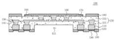
도 1을 참조하면, 본 발명의 실시 예에 따른 패키지 기판(100)은 절연층(130), 접속 패드(110), 내층 회로 패턴(150), 외층 회로 패턴(170), 제1 비아(140), 제2 비아(160) 및 보호층(180)을 포함한다.Referring to FIG. 1, a
본 발명의 실시 예에 따르면, 절연층(130)은 통상적으로 층간 절연소재로 사용되는 복합 고분자 수지로 형성될 수 있다. 예를 들어, 절연층(130)은 프리프레그, ABF(Ajinomoto Build up Film) 및 FR-4, BT(Bismaleimide Triazine) 등의 에폭시계 수지로 형성될 수 있다. 그러나 본 발명의 실시 예에서 절연층(130)을 형성하는 물질이 이에 한정되는 것은 아니다. 본 발명의 실시 예에 따른 절연층(130)은 회로 기판 분야에서 공지된 절연재 중에서 선택될 수 있다.According to an embodiment of the present invention, the insulating layer 130 may be formed of a composite polymer resin, which is typically used as an interlayer insulating material. For example, the insulating layer 130 may be formed of an epoxy resin such as prepreg, ABF (Ajinomoto Build-up Film), FR-4, and BT (Bismaleimide Triazine). However, the material forming the insulating layer 130 in the embodiment of the present invention is not limited thereto. The insulating layer 130 according to embodiments of the present invention may be selected from those known in the field of circuit boards.
본 발명의 실시 예에서 절연층(130)은 제1 절연층(131)과 제2 절연층(135)으로 구분된다. 제2 절연층(135)은 제1 절연층(131) 상부에 형성된다.In the embodiment of the present invention, the insulating layer 130 is divided into a first
도 1에서는 제1 절연층(131)과 제2 절연층(135)이 동일한 재질로 형성되는 것으로 도시되어 있다. 그러나 본 발명의 실시 예에서 제1 절연층(131)과 제2 절연층(135)이 동일한 재질로 형성되는 것으로 한정되지 않는다. 예를 들어, 제1 절연층(131)은 유리 섬유가 포함된 절연재로 형성되며, 제2 절연층(135)은 유리 섬유가 미포함된 절연재로 형성될 수 있다. 이와 같이, 제1 절연층(131)과 제2 절연층(135)의 재질은 당업자의 선택에 따라 변경될 수 있다.In FIG. 1, the first
본 발명의 실시 예에 따르면, 제1 절연층(131)에는 하면에서 내부로 소정의 깊이를 갖는 홈인 캐비티(121)가 형성된다. 본 발명의 실시 예에 따른 캐비티(121)의 내부에는 적층형 패키지를 형성할 때, 하부 패키지의 전자 소자가 위치하게 된다. 따라서, 본 발명의 실시 예에 따른 캐비티(121)는 추후 내부에 전자소자의 적어도 일부가 삽입될 수 있을 정도의 크기를 갖도록 형성된다.According to the embodiment of the present invention, the first insulating
본 발명의 실시 예에 따르면, 접속 패드(110)는 제1 절연층(131)의 내부에 형성되며, 캐비티(121)의 양측에 형성된다. 도 1에서는 접속 패드(110)가 캐비티(121)의 좌우에 형성되는 것으로 도시되었지만, 접속 패드(110)는 캐비티(121)의 측면 테두리를 둘러싸도록 형성될 수 있다.According to the embodiment of the present invention, the
본 발명의 실시 예에 따르면, 접속 패드(110)는 제1 절연층(131)과 동일하거나 얇은 두께를 갖도록 형성된다. 여기서, 본 발명의 실시 예에 따른 접속 패드(110)는 캐비티(121)의 깊이와 대응되는 두께를 갖도록 형성된다. 예를 들어, 도 1에 도시된 바와 같이 접속 패드(110)는 캐비티(121)의 깊이와 동일한 두께를 갖도록 형성된다.According to the embodiment of the present invention, the
본 발명의 실시 예에서 접속 패드(110)는 도 1에 도시된 바와 같이 다른 회로 패턴들보다 더 두꺼운 두께를 갖도록 형성된다.In the embodiment of the present invention, the
본 발명의 실시 예에 따른 접속 패드(110)의 하부에는 금속층(520)이 형성될 수 있다. 금속층(520)은 접속 패드(110)의 하부에 형성되어, 제1 절연층(131)으로부터 돌출되는 구조를 갖는다.A
본 발명의 실시 예에 따른 접속 패드(110)와 금속층(520)은 구리(Cu)로 형성된다. 그러나 접속 패드(110)와 금속층(520)의 재질이 구리로 한정되는 것은 아니며, 회로 기판 분야에서 사용되는 전도성 물질 중 것도 될 수 있다.The
본 발명의 실시 예에 따르면, 내층 회로 패턴(150)은 절연층(130)의 내부에 형성된다. 예를 들어, 내층 회로 패턴(150)은 제1 절연층(131)의 상부에 형성되며, 제2 절연층(135)에 매립되도록 형성될 수 있다. 본 발명의 실시 예에서, 내층 회로 패턴(150)이 1층으로 형성되는 것으로 도시 및 설명하지만, 이에 한정되지 않는다. 즉, 본 발명의 실시 예에 따른 내층 회로 패턴(150)은 당업자의 선택에 따라 2층 이상의 다층으로 형성될 수 있다.According to the embodiment of the present invention, the inner
본 발명의 실시 예에 따르면, 외층 회로 패턴(170)은 제2 절연층(135)의 상부에 형성된다.According to the embodiment of the present invention, the outer
본 발명의 실시 예에 따른 내층 회로 패턴(150)과 외층 회로 패턴(170)은 구리(Cu)로 형성될 수 있다. 그러나 내층 회로 패턴(150)과 외층 회로 패턴(170)의 재질이 구리로 한정되는 것은 아니며, 회로 기판 분야에서 사용되는 전도성 물질 중 것도 될 수 있다.The inner
본 발명의 실시 예에 따르면, 제1 비아(140)는 제1 절연층(131)의 내부에 형성된다. 본 발명의 실시 예에 따르면, 제1 비아(140)의 하면은 접속 패드(110)와 접합되며, 상면은 내층 회로 패턴(150)에 접합된다. 이와 같이 형성된 제1 비아(140)는 접속 패드(110)와 내층 회로 패턴(150)을 전기적으로 연결한다.According to an embodiment of the present invention, the
본 발명의 실시 예에 따르면, 접속 패드(110), 제1 비아(140) 및 금속층(520)에 의해서 패키지 기판(100)의 외부에 위치한 외부 구성부와 내층 회로 패턴(150)이 전기적으로 연결된다. 따라서, 본 발명의 실시 예에 따른 접속 패드(110)와 제1 비아(140)의 두께의 합은 내층 회로 패턴(150)과 금속층(520)을 전기적으로 연결할 수 있을 정도이다. 따라서, 여기서, 외부 구성부는 예를 들어, 전자 소자, 패키지, 메인 보드 등이 될 수 있다.According to the embodiment of the present invention, the external component located outside the
또한, 하부 패키지 기판(미도시)에 본 발명의 실시 예에 따른 패키지 기판(100)이 적층될 때, 캐비티(121), 접속 패드(110) 및 제1 비아(140)에 의해서 하부 패키지 기판과의 간격이 좁아진다. 따라서, 간격이 좁아진 만큼 하부 패키지 기판과의 연결을 위한 외부 접속 단자(미도시)의 크기도 작아질 수 있다.When the
본 발명의 실시 예에 따른 제2 비아(160)는 제2 절연층(135)의 내부에 형성된다. 본 발명의 실시 예에 따르면, 제2 비아(160)의 하면은 내층 회로 패턴(150)과 접합되며, 상면은 외층 회로 패턴(170)과 접합된다. 이와 같이 형성된 제2 비아(160)는 내층 회로 패턴(150)과 외층 회로 패턴(170)을 전기적으로 연결한다.A second via 160 according to an embodiment of the present invention is formed within the second insulating
본 발명의 실시 예에 따르면, 보호층(180)은 제2 절연층(135)과 외층 회로 패턴(170)의 상부에 형성된다. 본 발명의 실시 예에 따른 보호층(180)은 외층 회로 패턴(170)이 추후 전자 소자(미도시)의 실장을 위한 솔더링(Soldering)이 수행될 때, 솔더가 도포되는 것을 방지할 수 있다. 또한, 보호층(180)은 외층 회로층이 산화 및 부식되는 것을 방지할 수 있다.According to an embodiment of the present invention, the
본 발명의 실시 예에 따른 보호층(180)은 외층 회로 패턴(170)의 일부를 노출하도록 형성된다. 이때, 보호층(180)에 의해서 노출되는 외층 회로 패턴(170)은 전자 소자와 같은 외부 구성부와 전기적으로 연결되는 영역이 될 수 있다.The
또한, 본 발명의 실시 예에 따르면, 보호층(180)은 제1 절연층(131)의 하부에 형성되어 금속층(520)을 노출하도록 형성된다. 이때, 보호층(180)에 의해서 노출되는 금속층(520)은 외부 구성부와 전기적으로 연결되는 영역이 될 수 있다.In addition, according to an embodiment of the present invention, the
본 발명의 실시 예에 따르면, 보호층(180)은 내열성 피복 재료로 형성된다. 예를 들어, 보호층(180)은 솔더 레지스트로 형성될 수 있다.According to an embodiment of the present invention, the
본 발명의 실시 예에 따르면, 보호층(180)은 당업자의 선택에 따라 형성되는 영역을 변경할 수 있으며, 생략되는 것도 가능하다.According to the embodiment of the present invention, the
본 발명의 실시 예에 따르면, 표면 처리층(190)은 보호층(180)에 의해 노출된 외층 회로 패턴(170)에 형성된다. 또한, 표면 처리층(190)은 보호층(180)에 의해 노출된 금속층(520)에 형성된다. 표면 처리층(190)은 보호층(180)에 의해 노출된 외층 회로 패턴(170) 및 금속층(520)이 부식 및 산화되는 것을 방지하기 위해서 형성된다. 예를 들어, 표면 처리층(190)은 니켈, 주석, 금, 팔라듐 등을 도금하거나 유기물 보호막(Organic Solder ability Preservative; OSP)을 코팅하는 것과 같이 회로 기판 분야에서 공지된 어떠한 표면 처리층도 가능하다.According to an embodiment of the present invention, the
본 발명의 실시 예에 따른 표면 처리층(190)은 당업자의 선택에 따라 생략될 수 있다.The
또한, 도 1에는 미도시 되었지만, 패키지 기판(100)의 하부에는 외부 접속 단자(미도시)가 형성될 수 있다. 외부 접속 단자는 솔더 볼일 수 있다.Although not shown in FIG. 1, external connection terminals (not shown) may be formed under the
또한, 본 발명의 실시 예에서, 접속 패드(110)의 두께가 캐비티(121)의 깊이 정도를 갖도록 형성되어, 내층 회로 패턴(150)과 전기적 연결을 위해 제1 비아(140)가 형성되는 것을 예시로 설명하였지만, 이에 한정되지 않는다. 예를 들어, 본 발명의 실시 예에 따른 접속 패드(110)가 제1 절연층(131)을 관통하는 두께로 형성되면 내층 회로 패턴(150)과 직접 접합되며, 제1 비아(140)는 생략될 수 있다.In the embodiment of the present invention, the thickness of the
본 발명의 실시 예에 따른 패키지 기판(100)은 내부에 하부 패키지 기판의 전자 소자가 배치되는 캐비티(121)와 하부 패키지와의 간격을 좁혀주는 접속 패드(110)를 포함한다. 따라서, 추후 적층형 패키지가 형성될 때, 본 발명의 실시 예에 따른 패키지 기판(100)에 의해서 적층형 패키지 전체의 두께가 감소될 수 있다. 본 발명의 실시 예에 따른 패키지 기판(100)이 적용된 적층형 패키지에 대한 설명은 추후 도 17에서 설명하도록 한다.
The
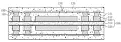
도 2를 참조하면, 캐리어 기판(500)이 제공된다.Referring to FIG. 2, a
본 발명의 실시 예에 따른 캐리어 기판(500)은 패키지 기판을 위한 절연층 및 회로층이 형성될 때, 이를 지지하기 위한 구성이다.The
본 발명의 실시 예에 따르면, 캐리어 기판(500)은 캐리어 코어(510)에 금속층(520)이 적층된 구조이다.According to the embodiment of the present invention, the
예를 들어, 캐리어 코어(510)는 절연 재질로 형성된다. 그러나 캐리어 코어(510)의 재질이 절연 재질로 한정되는 것은 아니며, 금속 재질 또는 절연층과 금속층이 한 층 이상 적층된 구조일 수 있다.For example, the
예를 들어, 금속층(520)은 구리(Cu)로 형성된다. 그러나 금속층(520)의 재질이 구리로 한정되는 것은 아니며, 회로 기판 분야에서 사용되는 전도성 물질이라면 제한 없이 적용될 수 있다.For example, the
본 발명의 실시 예에서 캐리어 기판(500)은 캐리어 코어(510)의 양면에 1층의 금속층(520)이 적층된 구조로 도시 및 설명되어 있으나, 캐리어 기판(500)의 구조는 이에 한정되지 않는다. 즉, 본 발명의 실시 예에서 캐리어 기판(500)은 설명과 이해의 편의를 위해서 간략하게 도시된 것이다. 예를 들어, 캐리어 기판(500)은 캐리어 코어에 다층의 금속층이 적층되며, 다층의 금속층 사이에 이형층이 형성된 것일 수 있다. 따라서 추후 이형층이 분리되면서 최외층에 형성된 금속층을 제외한 캐리어 기판이 패키지 기판으로부터 분리 및 제거될 수 있다. 이와 같이 캐리어 기판(500)의 구조는 본 발명의 실시 예로 도시 및 설명된 구조에 한정되는 것은 아니다. 즉, 해당 기술 분야에서 사용되는 어떠한 구조의 캐리어 기판도 본 실시 예에 적용 가능하다.
In the embodiment of the present invention, the
도 3을 참조하면, 캐리어 기판(500)에 도금 레지스트(530)가 형성된다.Referring to FIG. 3, a plating resist 530 is formed on the
본 발명의 실시 예에 따르면, 도금 레지스트(530)는 캐리어 기판(500)의 금속층(520) 상부에 형성된다. 또한, 본 발명의 실시 예에 따른 도금 레지스트(530)는 접속 패드(미도시)와 캐비티 패턴(미도시)이 형성될 영역의 금속층(520)을 노출하는 개구부(531)를 갖는다. 여기서 캐비티 패턴이 형성될 영역은 전자 소자가 실장될 수 있을 정도의 크기를 갖도록 형성된다.
According to an embodiment of the present invention, a plating resist 530 is formed on the
도 4를 참조하면, 캐리어 기판(500)에 접속 패드(110)와 캐비티 패턴(120)이 형성된다.Referring to FIG. 4, a
본 발명의 실시 예에 따르면, 접속 패드(110)와 캐비티 패턴(120)은 캐리어 기판(500)의 금속층(520) 상부에 형성된다.According to an embodiment of the present invention, the
본 발명의 실시 예에 따르면, 접속 패드(110)와 캐비티 패턴(120)은 도금 레지스트(530)의 개구부(531)에 전해 도금을 수행하여 형성된다. 이때, 도금 레지스트(530)의 개구부(531)를 통해서 노출된 금속층(520)이 전해 도금을 위한 시드(Seed)층의 역할을 할 수 있다.According to the embodiment of the present invention, the
본 발명의 실시 예에 따른 접속 패드(110)는 외부의 구성부와 전기적으로 연결되는 회로 패턴이다.The
또한, 캐비티 패턴(120)은 적층형 패키지가 형성될 때, 하부 패키지 기판상에 실장된 전자 소자가 위치하는 공간을 확보하기 위해서 형성된다. 따라서, 캐비티 패턴(120)은 추후 전자 소자가 캐비티(미도시) 내부에 위치할 수 있을 정도의 크기를 갖도록 형성된다.In addition, the
본 발명의 실시 예에서, 접속 패드(110)가 캐비티 패턴(120)과 동일한 공정으로 형성되므로 동일한 두께를 갖도록 형성된다. 그러나 접속 패드(110)가 캐비티 패턴(120)과 반드시 동일한 두께를 갖도록 형성되는 것은 아니다. 당업자의 선택에 따라 접속 패드(110)는 캐비티 패턴(120)보다 더 두껍게 형성되거나 더 얇게 형성될 수 있다.
In the embodiment of the present invention, the
도 5를 참조하면, 도금 레지스트(도 4의 530)가 제거된다.
Referring to Fig. 5, the plating resist (530 in Fig. 4) is removed.
도 6을 참조하면, 제1 절연층(131)이 형성된다.Referring to FIG. 6, a first insulating
본 발명의 실시 예에 따르면, 제1 절연층(131)은 금속층(520)의 상부에 형성되어 접속 패드(110)와 캐비티 패턴(120)을 덮도록 형성된다. 본 발명의 실시 예에 따르면, 제1 절연층(131)의 상면은 접속 패드(110)의 상면과 캐비티 패턴(120)의 상면보다 높게 위치하도록 형성된다. 즉, 제1 절연층(131)은 접속 패드(110)와 캐비티 패턴(120)의 상부에도 소정의 두께를 갖도록 형성될 수 있다.The first insulating
본 발명의 실시 예에 따르면, 제1 절연층(131)은 액상 형태로 금속층(520), 접속 패드(110) 및 캐비티 패턴(120)의 상부에 도포하는 방법으로 형성될 수 있다. 또는 제1 절연층(131)은 필름 형태로 금속층(520), 접속 패드(110) 및 캐비티 패턴(120)의 상부에 적층한 후 가압하는 방법으로 형성될 수 있다. 본 발명의 실시 예에 따른 제1 절연층(131)은 상술한 방법뿐만 아니라 회로 기판 분야에서 절연층을 형성하는 어떠한 방법으로도 형성될 수 있다.According to an embodiment of the present invention, the first insulating
본 발명의 실시 예에 따른 제1 절연층(131)은 통상적으로 층간 절연소재로 사용되는 복합 고분자 수지로 형성될 수 있다. 예를 들어, 제1 절연층(131)은 프리프레그, ABF(Ajinomoto Build up Film) 및 FR-4, BT(Bismaleimide Triazine) 등의 에폭시계 수지로 형성될 수 있다. 그러나 본 발명의 실시 예에서 제1 절연층(131)을 형성하는 물질이 이에 한정되는 것은 아니다. 본 발명의 실시 예에 따른 제1 절연층(131)은 회로 기판 분야에서 공지된 절연재 중에서 선택될 수 있다.
The first insulating
도 7을 참조하면, 내층 회로 패턴(150) 및 제1 비아(140)가 형성된다.Referring to FIG. 7, an inner
본 발명의 실시 예에 따르면, 내층 회로 패턴(150)은 제1 절연층(131)의 상부에 형성되며, 제1 비아(140)는 제1 절연층(131)의 내부에 형성된다.The inner
본 발명의 실시 예에 따른 제1 비아(140)는 접속 패드(110) 상부에 형성된 제1 절연층(131)에 형성된다. 즉, 제1 비아(140)는 접속 패드(110) 상부에 형성된 제1 절연층(131)을 관통하여, 상면은 내층 회로 패턴(150)과 접합되고 하면은 접속 패드(110)에 접합되도록 형성된다. 이와 같이 형성된 제1 비아(140)에 의해서 내층 회로 패턴(150)과 접속 패드(110)가 전기적으로 연결된다.The first via 140 according to the embodiment of the present invention is formed on the first insulating
본 발명의 실시 예에 따른 내층 회로 패턴(150)과 제1 비아(140)는 비아홀(미도시)을 가공하고 패터닝된 도금 레지스트(미도시)를 형성한 후, 도금을 수행하여 형성될 수 있다. 또는 본 발명의 실시 예에 따른 내층 회로 패턴(150)과 제1 비아(140)는 비아홀을 가공하고 도금을 수행한 후 에칭 레지스트 형성하여 에칭 공정을 수행하여 형성될 수 있다. 상술한 방법은 내층 회로 패턴(150)과 제1 비아(140)를 형성하는 방법에 대한 예시 중 일부이며, 내층 회로 패턴(150)과 제1 비아(140)는 회로 기판 분야에서 공지된 어떠한 방법으로 형성될 수 있다.The inner
또한, 본 발명의 실시 예에 따른 내층 회로 패턴(150)과 제1 비아(140)는 회로 기판 분야에서 사용되는 어떠한 전도성 물질로도 형성될 수 있다. 예를 들어, 내층 회로 패턴(150)과 제1 비아(140)는 구리(Cu)로 형성될 수 있다.In addition, the inner
본 발명의 실시 예에서는 내층 회로 패턴(150)이 한 층으로 형성되는 것을 예시로 설명하였지만, 이와 같은 구조로 본 발명이 한정되지 않는다. 즉, 본 발명의 실시 예에 따른 내층 회로 패턴(150)은 당업자의 선택에 따라 다층으로 형성될 수 있다. 이와 같은 경우, 제1 절연층(131)도 다층으로 형성될 수 있으며, 각 층의 내층 회로 패턴(150)을 서로 연결하는 비아도 더 형성될 수 있다.
In the embodiment of the present invention, the inner
도 8을 참조하면, 제2 절연층(135)이 형성된다.Referring to FIG. 8, a second insulating
본 발명의 실시 예에 따르면, 제2 절연층(135)은 제1 절연층(131)의 상부에 형성되어 내층 회로 패턴(150)을 덮도록 형성된다.According to an embodiment of the present invention, the second insulating
본 발명의 실시 예에 따르면, 제2 절연층(135)은 액상 형태로 제1 절연층(131)과 내층 회로 패턴(150)의 상부에 도포하는 방법으로 형성될 수 있다. 또는 제2 절연층(135)은 필름 형태로 제1 절연층(131)과 내층 회로 패턴(150)의 상부에 적층한 후 가압하는 방법으로 형성될 수 있다. 본 발명의 실시 예에 따른 제2 절연층(135)은 상술한 방법뿐만 아니라 회로 기판 분야에서 절연층을 형성하는 어떠한 방법으로도 형성될 수 있다.According to an embodiment of the present invention, the second insulating
본 발명의 실시 예에 따르면, 제2 절연층(135)은 통상적으로 사용되는 층간 절연 소재 중에서 유리 섬유가 함유되지 않은 절연 재질로 형성될 수 있다. 그러나 제2 절연층(135)의 재질이 이에 한정되지 않는다. 즉, 본 발명의 실시 예에 따른 제2 절연층(135)은 회로 기판 분야에서 사용되는 통상적인 층간 절연소재 중에서 어떠한 것도 가능하며, 제1 절연층(131)과 동일한 재질로 형성될 수 있다.
According to an embodiment of the present invention, the second insulating
도 9를 참조하면, 외층 회로 패턴(170) 및 제2 비아(160)가 형성된다.Referring to FIG. 9, an outer
본 발명의 실시 예에 따르면, 외층 회로 패턴(170)은 제2 절연층(135)의 상부에 형성되며, 제2 비아(160)는 제2 절연층(135)의 내부에 형성된다.The outer
본 발명의 실시 예에 따른 외층 회로 패턴(170)은 패키지 기판(100)의 최외층에 형성되는 회로 패턴이다. 따라서, 외층 회로 패턴(170)의 일부 패턴은 전자 소자, 패키지, 기판 등과 같은 외부 구성부와 전기적으로 접속될 수 있다.The outer
본 발명의 실시 예에 따른 제2 비아(160)는 제2 절연층(135)을 관통하여, 상면은 외층 회로 패턴(170)과 접합되고 하면은 내층 회로 패턴(150)과 접합되도록 형성된다. 이와 같이 형성된 제2 비아(160)에 의해서 내층 회로 패턴(150)과 외층 회로 패턴(170)이 전기적으로 연결된다.The second via 160 according to the embodiment of the present invention is formed so as to penetrate the second insulating
본 발명의 실시 예에 따른 외층 회로 패턴(170)과 제2 비아(160)를 형성하는 방법과 재질은 도 7의 내층 회로 패턴(150)과 제1 비아(140)를 형성하는 방법과 재질을 참고하도록 한다.
The method and material of forming the outer
도 10을 참조하면, 보호층(180)이 형성된다.Referring to FIG. 10, a
본 발명의 실시 예에 따르면, 보호층(180)은 제2 절연층(135)과 외층 회로 패턴(170)의 상부에 형성된다. 본 발명의 실시 예에 따른 보호층(180)은 외층 회로 패턴(170)이 추후 전자 소자(미도시)의 실장을 위한 솔더링(Soldering)이 수행될 때, 솔더가 도포되는 것을 방지할 수 있다. 도한, 보호층(180)은 외층 회로층이 산화 및 부식되는 것을 방지할 수 있다.According to an embodiment of the present invention, the
본 발명의 실시 예에 따른 보호층(180)은 외층 회로 패턴(170)의 일부를 노출하도록 형성된다. 이때, 보호층(180)에 의해서 노출되는 외층 회로 패턴(170)은 전자 소자와 같은 외부 구성부와 전기적으로 연결되는 영역이 될 수 있다.The
본 발명의 실시 예에 따르면, 보호층(180)은 내열성 피복 재료로 형성된다. 예를 들어, 보호층(180)은 솔더 레지스트로 형성될 수 있다.
According to an embodiment of the present invention, the
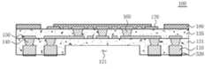
도 11을 참조하면, 캐리어 기판(500)이 제거된다.Referring to FIG. 11, the
본 발명의 실시 예에 따르면, 캐리어 코어(510)와 금속층(520)을 분리한 후, 캐리어 코어(510)를 제거한다. 캐리어 코어(510)가 제거되면, 캐리어 기판(500)의 양면에 각각 형성된 패키지 기판(100)이 분리된다.
According to an embodiment of the present invention, after the
도 12를 참조하면, 에칭 레지스트(540)가 형성된다.Referring to FIG. 12, an etching resist 540 is formed.
본 발명의 실시 예에 따른 에칭 레지스트(540)는 추후 캐비티 패턴(120)이 에칭될 때, 접속 패드(110)가 손상되는 것을 방지하기 위해서 형성된다. 따라서, 에칭 레지스트(540)는 접속 패드(110)를 에칭 공정으로부터 보호하기 위해서 접속 패드(110)의 하부에 형성된다. 이때, 에칭 레지스트(540)는 접속 패드(110)가 형성된 영역에 위치한 금속층(520)의 일부도 동시에 보호한다.The etching resist 540 according to the embodiment of the present invention is formed to prevent the
본 발명의 실시 예에 따른 에칭 레지스트(540)는 접속 패드(110)가 형성된 영역 이외의 영역을 노출하도록 개구부(541)가 형성된다.The etching resist 540 according to the embodiment of the present invention is formed with the
또한, 본 발명의 실시 예에 따른 에칭 레지스트(540)는 만약 이후 진행되는 에칭 공정이 에칭액을 이용하는 경우, 해당 에칭액에 반응하지 않는 재질로 형성되어야 한다.
In addition, the etching resist 540 according to the embodiment of the present invention should be formed of a material that does not react with the etching solution, if a subsequent etching process uses an etching solution.
도 13을 참조하면, 캐비티(121)가 형성된다.Referring to Fig. 13, a
본 발명의 실시 예에 따르면, 에칭 공정이 수행된다. 에칭 공정에 의해서 에칭 레지스트(540)의 개구부(541)에 의해서 노출된 영역의 금속층(520)과 캐비티 패턴(120)이 제거된다.According to an embodiment of the present invention, an etching process is performed. The
본 발명의 실시 예에 따르면, 에칭 공정은 캐비티 패턴(120)과 금속층(520)이 반응하는 에칭액으로 수행될 수 있다. 이때, 에칭 레지스트(540)는 사용되는 에칭액에 반응하지 않아야 한다.According to an embodiment of the present invention, the etching process may be performed with an etchant in which the
본 발명의 실시 예에 따르면, 에칭 공정에 의해서 캐비티 패턴(120)이 제거되어, 캐비티(121)가 형성된다. 이와 같이 형성된 캐비티(121)에는 추후 전자 소자(미도시)가 위치할 수 있다.According to the embodiment of the present invention, the
본 발명의 실시 예에서, 캐비티 패턴(120)의 제거를 위해 에칭액을 이용하지만, 캐비티 패턴(120)을 제거하는 에칭 공정이 이에 한정되는 것은 아니다. 즉, 캐비티 패턴(120) 회로 기판 분야에서 공지된 에칭 방법 중 어떠한 방법으로도 제거될 수 있다.In the embodiment of the present invention, although the etching liquid is used for removing the
본 발명의 실시 예에 따르면, 에칭 공정이 수행될 때, 에칭 레지스트(540)에 의해서 접속 패드(110)와 접속 패드(110)와 에칭 레지스트(540) 사이에 위치한 금속층(520)도 에칭되지 않고 보호된다.
According to the embodiment of the present invention, when the etching process is performed, the
도 14를 참조하면, 에칭 레지스트(도 13의 540)가 제거된다.Referring to Fig. 14, the etching resist (540 in Fig. 13) is removed.
본 발명의 실시 예에 따르면, 에칭 레지스트(도 13의 540)에 의해 접속 패드(110)의 하부에 형성된 금속층(520)은 에칭 공정으로부터 보호된다. 따라서, 에칭 레지스트(도 13의 540)가 제거되면, 보호된 금속층(520)은 도시된 바와 같이 제1 절연층(131)의 하면으로부터 돌출된다.
According to an embodiment of the present invention, the
도 15를 참조하면, 표면 처리층(190)이 형성될 수 있다.Referring to FIG. 15, a
본 발명의 실시 예에 따르면, 제1 절연층(131) 하부에 보호층(180)이 형성된다. 제1 절연층(131)의 하부에 형성된 보호층(180)은 금속층(520)이 외부로 노출되도록 형성된다. 이때, 외부로 노출되는 금속층(520)은 추후 외부 접속 단자(미도시)와 연결되는 부분이다.According to an embodiment of the present invention, a
본 발명의 실시 예에 따른 제1 절연층(131) 하부에 형성되는 보호층(180)은 반드시 이 단계에서 형성되어야 하는 것은 아니다. 보호층(180)은 금속층(520)이 패터닝된 이후 단계 중 어느 단계에서도 형성 가능하다. 또한, 본 발명의 실시 예에 따른 제1 절연층(131) 하부에 형성되는 보호층(180)은 당업자의 선택에 따라 생략되는 것도 가능하다.The
본 발명의 실시 예에 따르면, 표면 처리층(190)은 보호층(180)에 의해 노출된 외층 회로 패턴(170)에 형성된다. 또한, 본 발명의 실시 예에 따르면, 표면 처리층(190)은 보호층(180)에 의해 노출된 금속층(520)에 형성된다.According to an embodiment of the present invention, the
본 발명의 실시 예에 따른 표면 처리층(190)은 보호층(180)에 의해 노출된 외층 회로 패턴(170) 및 금속층(520)이 부식 및 산화되는 것을 방지하기 위해서 형성된다. 예를 들어, 표면 처리층(190)은 니켈, 주석, 금, 팔라듐 등을 도금하거나 유기물 보호막(Organic Solder ability Preservative; OSP)을 코팅하는 것과 같이 회로 기판 분야에서 공지된 표면 처리 방법으로 형성될 수 있다.The
본 발명의 실시 예에 따른 표면 처리층(190)을 형성하는 단계는 당업자의 선택에 따라 생략되거나, 외층 회로 패턴(170)이 형성된 이후라면 형성 단계가 변경될 수 있다. 또한, 본 발명의 실시 예에 따른 표면 처리층(190)은 당업자의 선택에 따라 외층 회로 패턴(170)과 금속층(520) 중에서 원하는 패턴에만 선택적으로 형성되는 것도 가능하다.
The step of forming the
도 16을 참조하면, 외부 접속 단자(195)가 형성된다.16, an external connection terminal 195 is formed.
본 발명의 실시 예에 따르면, 외부 접속 단자(195)는 금속층(520) 하부에 형성된 표면 처리층(190) 중에서 보호층(180)에 의해 외부로 노출된 표면 처리층(190)의 하면에 형성된다. 또는 표면 처리층(190)과 보호층(180)이 생략된 경우, 외부 접속 단자(195)는 제1 절연층(131)으로부터 노출된 접속 패드(110)의 하면에 형성된다. 본 발명의 실시 예에 따른 외부 접속 단자(195)는 기판, 패키지, 메인 보드 등과 같은 외부 구성부와 패키지 기판(100)을 전기적으로 연결하기 위한 구성부이다. 예를 들어, 외부 접속 단자(195)는 솔더 볼일 수 있다. 그러나 외부 접속 단자(195)의 형태가 볼 형태로 한정되는 것은 아니다.The external connection terminal 195 is formed on the lower surface of the
본 발명의 실시 예에 따라 제조된 패키지 기판(100)은 캐비티(121)가 형성되며, 적층형 패키지를 형성할 때, 캐비티(121)에 하부 패키지(미도시)의 전자 소자(미도시)가 위치하게 된다. 따라서, 캐비티(121)의 두께만큼 패키지 기판(100)과 하부 패키지 간의 간격이 더 좁아지게 된다. 따라서, 작은 크기의 외부 접속 단자(195)로 본 발명의 실시 예에 따른 패키지 기판(100)과 하부 패키지를 연결할 수 있다. 또한, 외부 접속 단자(195)의 크기가 작아짐에 따라 미세한 간격으로 외부 접속 단자(195)를 배치할 수 있으며, 외부 접속 단자(195) 간의 브리지(bridge)에 의한 불량이 발생하는 것을 방지 또는 감소할 수 있다.A
본 발명의 실시 예에 따른 패키지 기판(100)의 제조 방법은 도 2 내지 도 16에 한정되는 것은 아니다. 도 2 내지 도 16의 방법은 실시 예일 뿐, 캐리어 기판, 회로 패턴 형성 방법, 에칭 방법 등은 당업자의 선택에 따라 회로 기판 분야에서 공지된 구조 및 방법들 중에서 어느 것으로도 변경될 수 있다.
The manufacturing method of the
도 17은 본 발명의 실시 예에 따른 적층형 패키지를 나타낸 예시도이다.17 is an exemplary view showing a stacked package according to an embodiment of the present invention.
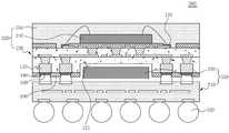
도 17을 참조하면, 본 발명의 실시 예에 따른 적층형 패키지(300)는 하부 패키지(310)에 상부 패키지(330)가 적층된 구조를 갖는다.Referring to FIG. 17, the
본 발명의 실시 예에 따르면, 하부 패키지(310)는 하부 패키지 기판(210) 및 제1 전자 소자(220)를 포함한다.According to an embodiment of the present invention, the
본 발명의 실시 예에 따른 하부 패키지 기판(210)은 절연층과 절연층에 형성된 회로 패턴을 포함한다. 하부 패키지 기판(210)의 상부에는 제1 전자 소자(220)가 배치된다.The
본 발명의 실시 예에 따른 제1 전자 소자(220)는 패키지 분야에 적용될 수 있는 어느 종류의 전자 소자도 될 수 있다.The first
또한, 본 발명의 실시 예에 따른 하부 패키지(310)의 하부에는 제1 외부 접속 단자(320)가 형성될 수 있다. 본 발명의 실시 예에 따른 제1 외부 접속 단자(320)는 솔더 볼일 수 있다.In addition, a first
본 발명의 실시 예에 따르면, 상부 패키지(330)는 상부 패키지 기판(230), 제2 전자 소자(240) 및 몰딩부(250)를 포함한다.In accordance with an embodiment of the present invention, the
본 발명의 실시 예에 따른 상부 패키지 기판(230)은 도 1의 패키지 기판(100)이다.The
본 발명의 실시 예에 따르면, 상부 패키지 기판(230)의 상부에는 제2 전자 소자(240)가 배치된다. 이때, 제2 전자 소자(240)는 와이어(Wire)를 통해 상부 패키지 기판(230)의 외층 회로 패턴(170)과 전기적으로 연결된다. 본 발명의 실시 예에서는 제2 전자 소자(240)와 상부 패키지 기판(230)을 와이어로 연결하는 것을 예시로 설명하였으나 이에 한정되는 것은 아니다. 즉, 제2 전자 소자(240)와 상부 패키지(330)는 솔더 범프, 솔더 볼과 같은 전도성 물질을 통해 전기적으로 연결될 수 있다. 또한, 본 발명의 실시 예에 따르면, 제2 전자 소자(240)는 메모리(Memory) 소자일 수 있다. 그러나 제2 전자 소자(240)의 종류가 메모리 소자로 한정되는 것은 아니며, 패키지 분야에 적용될 수 있는 어느 종류의 전자 소자도 될 수 있다.In accordance with an embodiment of the present invention, a second
본 발명의 실시 예에 따르면, 몰딩부(250)는 상부 패키지 기판(230)의 상부에 형성되어, 제2 전자 소자(240)를 덮도록 형성된다. 본 발명의 실시 예에 따른 몰딩부(250)는 제2 전자 소자(240)를 외부로부터 보호하기 위해서 형성된다. 예를 들어, 몰딩부(250)는 EMC(Epoxy Molding compound)로 형성될 수 있다. 그러나 몰딩부(250)의 재질이 EMC로 한정되는 것은 아니다.According to an embodiment of the present invention, the
또한, 본 발명의 실시 예에 따르면, 상부 패키지(330)의 하부에는 제2 외부 접속 단자(340)가 형성될 수 있다. 본 발명의 실시 예에 따른 제2 외부 접속 단자(340)는 도 16의 외부 접속 단자(195)이다.According to an embodiment of the present invention, a second
본 발명의 실시 예에 따르면, 상부 패키지(330)가 하부 패키지(310)에 적층될 때, 제1 전자 소자(220)가 상부 패키지 기판(230)의 캐비티(121) 내부에 위치하게 된다. 이때 캐비티(121)에 의해서 상부 패키지(330)와 하부 패키지(310) 간의 간격이 캐비티(121)의 깊이만큼 더 좁아진다. 또한, 캐비티(121)의 양측에 접속 패드(110)가 형성되어, 상부 패키지(330)의 내부와 제2 외부 접속 단자(340)를 전기적으로 연결한다. 따라서, 제2 외부 접속 단자(340)는 작은 크기의 솔더 볼로 형성되어도 상부 패키지(330)와 하부 패키지(310)를 충분히 연결할 수 있다. 이와 같이 제2 외부 접속 단자(340)는 작은 크기의 솔더 볼로 형성되므로, 다수개가 미세한 간격으로 배치될 수 있다. 또한, 제2 외부 접속 단자(340) 간의 브리지에 의한 불량이 발생하는 것을 방지 또는 감소할 수 있다. 또한, 작은 크기의 제2 외부 접속 단자(340)가 사용되므로 적층형 패키지(300)의 두께도 감소될 수 있다.
The first
이상 본 발명을 구체적인 실시 예를 통하여 상세히 설명하였으나, 이는 본 발명을 구체적으로 설명하기 위한 것으로, 본 발명은 이에 한정되지 않으며, 본 발명의 기술적 사상 내에서 당 분야의 통상의 지식을 가진 자에 의해 그 변형이나 개량이 가능함이 명백하다.
While the present invention has been particularly shown and described with reference to exemplary embodiments thereof, it is to be understood that the same is by way of illustration and example only and is not to be construed as limiting the present invention. It is obvious that the modification or improvement is possible.
본 발명의 단순한 변형 내지 변경은 모두 본 발명의 영역에 속하는 것으로 본 발명의 구체적인 보호 범위는 첨부된 특허청구범위에 의하여 명확해질 것이다.
It will be understood by those skilled in the art that various changes in form and details may be made therein without departing from the spirit and scope of the invention as defined by the appended claims.
100: 패키지 기판
110: 접속 패드
120: 캐비티 패턴
121: 캐비티
130: 절연층
131: 제1 절연층
135: 제2 절연층
140: 제1 비아
150: 내층 회로 패턴
160: 제2 비아
170: 외층 회로 패턴
180: 보호층
190: 표면 처리층
195: 외부 접속 단자
210: 하부 패키지 기판
220: 제1 전자 소자
230: 상부 패키지 기판
240: 제2 전자 소자
250: 몰딩부
300: 적층형 패키지
310: 하부 패키지
320: 제1 외부 접속 단자
330: 상부 패키지
340: 제2 외부 접속 단자
500: 캐리어 기판
510: 캐리어 코어
520: 금속층
530: 도금 레지스트
531, 541: 개구부
540: 에칭 레지스트100: Package substrate
110: connection pad
120: cavity pattern
121: cavity
130: insulating layer
131: first insulating layer
135: second insulating layer
140: 1st Via
150: Inner layer circuit pattern
160: Second Via
170: outer layer circuit pattern
180: protective layer
190: Surface treatment layer
195: External connection terminal
210: Lower package substrate
220: first electronic element
230: upper package substrate
240: second electronic element
250: Molding part
300: stacked package
310: Lower package
320: first external connection terminal
330: Upper package
340: second external connection terminal
500: carrier substrate
510: carrier core
520: metal layer
530: plating resist
531, 541:
540: etching resist
Claims (19)
Translated fromKorean상기 절연층의 하면에서 내부로 깊이를 갖도록 형성된 캐비티; 및
상기 절연층의 내부에 형성되며, 상기 캐비티의 적어도 일측에 형성된 접속패드;
를 포함하는 패키지 기판.
Insulating layer;
A cavity formed to have a depth from the lower surface of the insulating layer; And
A connection pad formed in the insulating layer and formed on at least one side of the cavity;
≪ / RTI >
상기 접속 패드는 상기 캐비티의 측면 테두리를 둘러싸도록 형성된 패키지 기판.
The method according to claim 1,
And the connection pad is formed to surround the side edge of the cavity.
상기 접속 패드는 상기 절연층과 동일하거나 얇은 두께를 갖도록 형성된 패키지 기판.
The method according to claim 1,
Wherein the connection pad has a thickness equal to or thinner than the insulation layer.
상기 절연층의 내부에 형성되며, 상기 접속 패드의 상면에 형성된 비아를 더 포함하는 패키지 기판.
The method according to claim 1,
And a via formed in the insulating layer and formed on an upper surface of the connection pad.
상기 접속 패드와 상기 접속 패드의 상면에 형성된 비아에 의해서 상기 절연층이 관통되는 패키지 기판.
The method of claim 4,
And the insulating layer is penetrated by the via formed on the upper surface of the connection pad and the connection pad.
상기 접속 패드의 하면에 형성된 금속층을 더 포함하는 패키지 기판.
The method according to claim 1,
And a metal layer formed on a lower surface of the connection pad.
상기 절연층 상부에 형성되어 상기 비아의 상면과 접합되는 내층 회로 패턴을 더 포함하는 패키지 기판.
The method of claim 4,
And an inner layer circuit pattern formed on the insulating layer and bonded to an upper surface of the via.
상기 캐리어 기판 상부에 형성되어 상기 접속 패드 및 캐비티 패턴을 매립하도록 형성된 절연층을 형성하는 단계;
상기 캐리어 기판을 제거하는 단계; 및
상기 캐비티 패턴을 제거하는 단계;
를 포함하는 패키지 기판의 제조 방법.
Forming a connection pad and a cavity pattern on the carrier substrate;
Forming an insulating layer formed on the carrier substrate to fill the connection pads and the cavity pattern;
Removing the carrier substrate; And
Removing the cavity pattern;
Wherein the package substrate has a first surface and a second surface.
상기 접속 패드 및 캐비티 패턴을 형성하는 단계에서,
상기 캐리어 기판은 캐리어 코어의 상부 또는 상하부에 금속층을 포함하는 패키지 기판의 제조 방법.
The method of claim 8,
In the step of forming the connection pad and the cavity pattern,
Wherein the carrier substrate comprises a metal layer on an upper portion or upper and lower portions of the carrier core.
상기 캐리어 기판을 제거하는 단계는,
상기 캐리어 코어와 금속층을 분리하여 상기 캐리어 코어를 제거하는 단계;
상기 금속층의 하부에 형성되며 상기 접속 패드와 대응되는 위치에 형성되는 에칭 레지스트를 형성하는 단계; 및
상기 에칭 레지스트에 의해 외부로 노출된 금속층을 제거하는 단계;
를 포함하는 패키지 기판의 제조 방법.
The method of claim 8,
Wherein the step of removing the carrier substrate comprises:
Separating the carrier core and the metal layer to remove the carrier core;
Forming an etching resist which is formed on a lower portion of the metal layer and is formed at a position corresponding to the connection pad; And
Removing the exposed metal layer by the etching resist;
Wherein the package substrate has a first surface and a second surface.
상기 접속 패드 및 캐비티 패턴을 형성하는 단계에서,
상기 접속 패드 및 캐비티 패턴은 전해 도금 방식으로 형성되는 패키지 기판의 제조 방법.
The method of claim 8,
In the step of forming the connection pad and the cavity pattern,
Wherein the connection pad and the cavity pattern are formed by an electrolytic plating method.
상기 절연층을 형성하는 단계 이후에,
상기 접속 패드 상면에 형성되어 상기 절연층을 관통하도록 형성되는 비아를 형성하는 단계를 더 포함하는 패키지 기판의 제조 방법.
The method of claim 8,
After the step of forming the insulating layer,
And forming a via formed on the upper surface of the connection pad so as to penetrate the insulating layer.
상기 비아를 형성하는 단계 또는 이후에,
상기 절연층의 상부에 형성되어 상기 비아의 상면과 접합되는 내층 회로 패턴을 형성하는 단계를 더 포함하는 패키지 기판의 제조 방법.
The method of claim 12,
The step of forming the vias, or thereafter,
And forming an inner layer circuit pattern formed on the insulating layer and bonded to an upper surface of the via.
절연층, 상기 절연층의 하면에서 내부로 깊이를 갖도록 형성된 캐비티 및 상기 절연층의 내부에 형성되며, 상기 캐비티의 적어도 일측에 형성된 접속패드를 포함하는 상부 패키지 기판을 포함하는 상부 패키지; 및
상기 하부 패키지 기판의 회로 패턴과 상기 상부 패키지 기판의 접속 패드 사이에 형성되어 상기 상부 패키지와 하부 패키지를 전기적으로 연결하는 외부 접속 단자;
를 포함하되,
상기 제1 전자 소자의 적어도 일부가 상기 캐비티에 삽입되는 적층형 패키지.
A lower package comprising a lower package substrate and a first electronic component disposed over the lower package substrate;
An upper package including an insulating layer, a cavity formed so as to have a depth from the lower surface of the insulating layer, and a connection pad formed inside the insulating layer and formed on at least one side of the cavity. And
An external connection terminal formed between a circuit pattern of the lower package substrate and a connection pad of the upper package substrate to electrically connect the upper package and the lower package;
, ≪ / RTI &
Wherein at least a portion of the first electronic component is inserted into the cavity.
상기 접속 패드는 상기 캐비티의 측면 테두리를 둘러싸도록 형성된 적층형 패키지.
15. The method of claim 14,
Wherein the connection pad is configured to surround a side edge of the cavity.
상기 절연층의 내부에 형성되며, 상기 접속 패드의 상면에 형성된 비아를 더 포함하는 적층형 패키지.
15. The method of claim 14,
And a via formed in the insulating layer and formed on an upper surface of the connection pad.
상기 접속 패드와 상기 접속 패드의 상면에 형성된 비아에 의해서 상기 절연층이 관통되는 적층형 패키지.
18. The method of claim 16,
Wherein the insulating layer is penetrated by the connection pad and a via formed on the upper surface of the connection pad.
상기 접속 패드의 하면에 형성되어, 상기 외부 접속 단자와 접촉되는 금속층을 더 포함하는 적층형 패키지.
15. The method of claim 14,
And a metal layer formed on a lower surface of the connection pad and in contact with the external connection terminal.
상기 절연층 상부에 형성되어 상기 비아의 상면과 접합되는 내층 회로 패턴을 더 포함하는 패키지 기판.18. The method of claim 16,
And an inner layer circuit pattern formed on the insulating layer and bonded to an upper surface of the via.
Priority Applications (4)
| Application Number | Priority Date | Filing Date | Title |
|---|---|---|---|
| KR1020140194133AKR20150135048A (en) | 2014-05-23 | 2014-12-30 | Printed circuit board, method for manufacturing the same and package on packaage having the thereof |
| TW104116329ATW201603665A (en) | 2014-05-23 | 2015-05-21 | Printed circuit board, method for manufacturing the same and package on package having the same |
| US14/719,309US20150342046A1 (en) | 2014-05-23 | 2015-05-21 | Printed circuit board, method for maufacturing the same and package on package having the same |
| CN201510271845.9ACN105101636A (en) | 2014-05-23 | 2015-05-25 | Printed circuit board, method for manufacturing the same and package on package having the same |
Applications Claiming Priority (2)
| Application Number | Priority Date | Filing Date | Title |
|---|---|---|---|
| KR20140062530 | 2014-05-23 | ||
| KR1020140062530 | 2014-05-23 |
Publications (1)
| Publication Number | Publication Date |
|---|---|
| KR20150135046Atrue KR20150135046A (en) | 2015-12-02 |
Family
ID=54883385
Family Applications (2)
| Application Number | Title | Priority Date | Filing Date |
|---|---|---|---|
| KR1020140174195APendingKR20150135046A (en) | 2014-05-23 | 2014-12-05 | Package board, method for manufacturing the same and package on packaage having the thereof |
| KR1020140194133ACeasedKR20150135048A (en) | 2014-05-23 | 2014-12-30 | Printed circuit board, method for manufacturing the same and package on packaage having the thereof |
Family Applications After (1)
| Application Number | Title | Priority Date | Filing Date |
|---|---|---|---|
| KR1020140194133ACeasedKR20150135048A (en) | 2014-05-23 | 2014-12-30 | Printed circuit board, method for manufacturing the same and package on packaage having the thereof |
Country Status (2)
| Country | Link |
|---|---|
| KR (2) | KR20150135046A (en) |
| TW (1) | TW201603665A (en) |
Cited By (1)
| Publication number | Priority date | Publication date | Assignee | Title |
|---|---|---|---|---|
| CN107731698A (en)* | 2017-10-26 | 2018-02-23 | 日月光半导体(上海)有限公司 | Ic package, package substrate and its manufacture method |
Families Citing this family (6)
| Publication number | Priority date | Publication date | Assignee | Title |
|---|---|---|---|---|
| US10163867B2 (en) | 2015-11-12 | 2018-12-25 | Amkor Technology, Inc. | Semiconductor package and manufacturing method thereof |
| KR101799668B1 (en)* | 2016-04-07 | 2017-11-20 | 앰코 테크놀로지 코리아 주식회사 | Semiconductor package and manufacturing method thereof |
| US10410999B2 (en) | 2017-12-19 | 2019-09-10 | Amkor Technology, Inc. | Semiconductor device with integrated heat distribution and manufacturing method thereof |
| US10506712B1 (en)* | 2018-07-31 | 2019-12-10 | Taiwan Semiconductor Manufacturing Co., Ltd. | Printed circuit board |
| KR102238223B1 (en)* | 2018-08-28 | 2021-04-09 | 성균관대학교산학협력단 | A method for flip-chip bonding using anisotropic adhesive polymer |
| US12211816B2 (en) | 2021-04-01 | 2025-01-28 | Samsung Electro-Mechanics Co., Ltd. | Printed circuit board and electronic component package including the same |
- 2014
- 2014-12-05KRKR1020140174195Apatent/KR20150135046A/enactivePending
- 2014-12-30KRKR1020140194133Apatent/KR20150135048A/ennot_activeCeased
- 2015
- 2015-05-21TWTW104116329Apatent/TW201603665A/enunknown
Cited By (2)
| Publication number | Priority date | Publication date | Assignee | Title |
|---|---|---|---|---|
| CN107731698A (en)* | 2017-10-26 | 2018-02-23 | 日月光半导体(上海)有限公司 | Ic package, package substrate and its manufacture method |
| CN107731698B (en)* | 2017-10-26 | 2024-03-26 | 日月光半导体(上海)有限公司 | Integrated circuit package, package substrate and manufacturing method thereof |
Also Published As
| Publication number | Publication date |
|---|---|
| TW201603665A (en) | 2016-01-16 |
| KR20150135048A (en) | 2015-12-02 |
Similar Documents
| Publication | Publication Date | Title |
|---|---|---|
| KR102425753B1 (en) | Printed circuit board, method for manufacturing the same and semiconductor package having the thereof | |
| KR102472945B1 (en) | Printed circuit board, semiconductor package and method of manufacturing the same | |
| KR102194722B1 (en) | Package board, method for manufacturing the same and package on package having the thereof | |
| JP5989814B2 (en) | Embedded substrate, printed circuit board, and manufacturing method thereof | |
| KR102186148B1 (en) | Embedded board and method of manufacturing the same | |
| KR20150135046A (en) | Package board, method for manufacturing the same and package on packaage having the thereof | |
| KR20170009128A (en) | Circuit board and manufacturing method of the same | |
| KR102194718B1 (en) | Embedded board and method of manufacturing the same | |
| US20150342046A1 (en) | Printed circuit board, method for maufacturing the same and package on package having the same | |
| KR20160099381A (en) | Printed circuit board and method of mamufacturing the same | |
| KR20160086181A (en) | Printed circuit board, package and method of manufacturing the same | |
| KR102254874B1 (en) | Package board and method for manufacturing the same | |
| KR20140143567A (en) | Semiconductor package board and method for maunfacturing the same | |
| US9491871B2 (en) | Carrier substrate | |
| US20150348918A1 (en) | Package substrate, package, package on package and manufacturing method of package substrate | |
| JP6798076B2 (en) | Embedded substrate and manufacturing method of embedded substrate | |
| KR102340053B1 (en) | Printed circuit board and method of manufacturing the same | |
| KR102473416B1 (en) | Printed circuit board and method of manufacturing the same | |
| KR102207272B1 (en) | Printed circuit board and method of manufacturing the same, and electronic component module | |
| JP6699043B2 (en) | Printed circuit board, manufacturing method thereof, and electronic component module | |
| KR20150065029A (en) | Printed circuit board, manufacturing method thereof and semiconductor package | |
| KR101300413B1 (en) | Printed circuit board for Semiconductor package and method for the same | |
| KR102240704B1 (en) | Package board, method of manufacturing the same and stack type package using the therof | |
| KR101103767B1 (en) | Printed circuit board and manufacturing method thereof | |
| KR20150142936A (en) | Package board and package using the same |
Legal Events
| Date | Code | Title | Description |
|---|---|---|---|
| PA0109 | Patent application | Patent event code:PA01091R01D Comment text:Patent Application Patent event date:20141205 | |
| PG1501 | Laying open of application | ||
| PC1204 | Withdrawal of earlier application forming a basis of a priority claim | Patent event date:20141205 Comment text:Patent Application Patent event code:PC12041R01I |