KR20150130519A - Wiring board - Google Patents
Wiring boardDownload PDFInfo
- Publication number
- KR20150130519A KR20150130519AKR1020157029234AKR20157029234AKR20150130519AKR 20150130519 AKR20150130519 AKR 20150130519AKR 1020157029234 AKR1020157029234 AKR 1020157029234AKR 20157029234 AKR20157029234 AKR 20157029234AKR 20150130519 AKR20150130519 AKR 20150130519A
- Authority
- KR
- South Korea
- Prior art keywords
- convex portion
- pad
- substrate
- opening
- layer
- Prior art date
- Legal status (The legal status is an assumption and is not a legal conclusion. Google has not performed a legal analysis and makes no representation as to the accuracy of the status listed.)
- Ceased
Links
- 229910000679solderInorganic materials0.000claimsabstractdescription107
- 239000000758substrateSubstances0.000claimsabstractdescription66
- 238000007747platingMethods0.000claimsdescription53
- 238000000034methodMethods0.000claimsdescription33
- 238000013459approachMethods0.000claimsdescription4
- RYGMFSIKBFXOCR-UHFFFAOYSA-NCopperChemical compound[Cu]RYGMFSIKBFXOCR-UHFFFAOYSA-N0.000description46
- 229920005989resinPolymers0.000description46
- 239000011347resinSubstances0.000description46
- 229910052802copperInorganic materials0.000description44
- 239000010949copperSubstances0.000description44
- PXHVJJICTQNCMI-UHFFFAOYSA-NNickelChemical compound[Ni]PXHVJJICTQNCMI-UHFFFAOYSA-N0.000description34
- 239000004020conductorSubstances0.000description31
- KDLHZDBZIXYQEI-UHFFFAOYSA-NPalladiumChemical compound[Pd]KDLHZDBZIXYQEI-UHFFFAOYSA-N0.000description24
- 229910052759nickelInorganic materials0.000description17
- 239000003822epoxy resinSubstances0.000description15
- 229920000647polyepoxidePolymers0.000description15
- PCHJSUWPFVWCPO-UHFFFAOYSA-NgoldChemical compound[Au]PCHJSUWPFVWCPO-UHFFFAOYSA-N0.000description13
- 229910052737goldInorganic materials0.000description13
- 239000010931goldSubstances0.000description13
- 239000011805ballSubstances0.000description12
- 239000000463materialSubstances0.000description12
- 229910052763palladiumInorganic materials0.000description12
- 238000004519manufacturing processMethods0.000description8
- 229920001187thermosetting polymerPolymers0.000description8
- 238000012545processingMethods0.000description6
- 238000010438heat treatmentMethods0.000description5
- XEEYBQQBJWHFJM-UHFFFAOYSA-NIronChemical compound[Fe]XEEYBQQBJWHFJM-UHFFFAOYSA-N0.000description4
- 229920000106Liquid crystal polymerPolymers0.000description4
- 239000013067intermediate productSubstances0.000description4
- 239000004977Liquid-crystal polymers (LCPs)Substances0.000description3
- 239000011248coating agentSubstances0.000description3
- 238000000576coating methodMethods0.000description3
- 239000011521glassSubstances0.000description3
- 238000002844meltingMethods0.000description3
- 230000008018meltingEffects0.000description3
- 230000000149penetrating effectEffects0.000description3
- 230000002093peripheral effectEffects0.000description3
- 239000000047productSubstances0.000description3
- 239000004065semiconductorSubstances0.000description3
- 238000004544sputter depositionMethods0.000description3
- CURLTUGMZLYLDI-UHFFFAOYSA-NCarbon dioxideChemical compoundO=C=OCURLTUGMZLYLDI-UHFFFAOYSA-N0.000description2
- BQCADISMDOOEFD-UHFFFAOYSA-NSilverChemical compound[Ag]BQCADISMDOOEFD-UHFFFAOYSA-N0.000description2
- 229910020836Sn-AgInorganic materials0.000description2
- 229910020988Sn—AgInorganic materials0.000description2
- 229910017052cobaltInorganic materials0.000description2
- 239000010941cobaltSubstances0.000description2
- GUTLYIVDDKVIGB-UHFFFAOYSA-Ncobalt atomChemical compound[Co]GUTLYIVDDKVIGB-UHFFFAOYSA-N0.000description2
- 239000002131composite materialSubstances0.000description2
- 239000011889copper foilSubstances0.000description2
- 239000000835fiberSubstances0.000description2
- 230000009477glass transitionEffects0.000description2
- 229910052742ironInorganic materials0.000description2
- LQBJWKCYZGMFEV-UHFFFAOYSA-Nlead tinChemical compound[Sn].[Pb]LQBJWKCYZGMFEV-UHFFFAOYSA-N0.000description2
- 229910052751metalInorganic materials0.000description2
- 239000002184metalSubstances0.000description2
- 239000007769metal materialSubstances0.000description2
- 229920001721polyimidePolymers0.000description2
- 239000009719polyimide resinSubstances0.000description2
- 229920001955polyphenylene etherPolymers0.000description2
- 229910052709silverInorganic materials0.000description2
- 239000004332silverSubstances0.000description2
- 238000009751slip formingMethods0.000description2
- 229910017944Ag—CuInorganic materials0.000description1
- 239000004593EpoxySubstances0.000description1
- 239000004952PolyamideSubstances0.000description1
- -1Sn-Ag-Inorganic materials0.000description1
- 229910009071Sn—Zn—BiInorganic materials0.000description1
- 239000000654additiveSubstances0.000description1
- 229910002092carbon dioxideInorganic materials0.000description1
- 239000001569carbon dioxideSubstances0.000description1
- 239000000919ceramicSubstances0.000description1
- 238000004891communicationMethods0.000description1
- 239000000805composite resinSubstances0.000description1
- 239000012141concentrateSubstances0.000description1
- 238000001816coolingMethods0.000description1
- 230000002950deficientEffects0.000description1
- 238000001514detection methodMethods0.000description1
- 238000011161developmentMethods0.000description1
- 238000005553drillingMethods0.000description1
- 230000000694effectsEffects0.000description1
- 238000007772electroless platingMethods0.000description1
- 238000009713electroplatingMethods0.000description1
- 238000005530etchingMethods0.000description1
- 230000005496eutecticsEffects0.000description1
- 239000004744fabricSubstances0.000description1
- 239000003365glass fiberSubstances0.000description1
- 238000010030laminatingMethods0.000description1
- 239000011806microballSubstances0.000description1
- 239000000203mixtureSubstances0.000description1
- 239000004745nonwoven fabricSubstances0.000description1
- 238000000059patterningMethods0.000description1
- 229920002647polyamidePolymers0.000description1
- 229920013636polyphenyl ether polymerPolymers0.000description1
- 239000004810polytetrafluoroethyleneSubstances0.000description1
- 229920001343polytetrafluoroethylenePolymers0.000description1
- 230000001681protective effectEffects0.000description1
- 238000012876topographyMethods0.000description1
Images


Classifications
- H—ELECTRICITY
- H01—ELECTRIC ELEMENTS
- H01L—SEMICONDUCTOR DEVICES NOT COVERED BY CLASS H10
- H01L23/00—Details of semiconductor or other solid state devices
- H01L23/48—Arrangements for conducting electric current to or from the solid state body in operation, e.g. leads, terminal arrangements ; Selection of materials therefor
- H01L23/488—Arrangements for conducting electric current to or from the solid state body in operation, e.g. leads, terminal arrangements ; Selection of materials therefor consisting of soldered or bonded constructions
- H01L23/498—Leads, i.e. metallisations or lead-frames on insulating substrates, e.g. chip carriers
- H01L23/49811—Additional leads joined to the metallisation on the insulating substrate, e.g. pins, bumps, wires, flat leads
- H01L23/49816—Spherical bumps on the substrate for external connection, e.g. ball grid arrays [BGA]
- H—ELECTRICITY
- H01—ELECTRIC ELEMENTS
- H01L—SEMICONDUCTOR DEVICES NOT COVERED BY CLASS H10
- H01L23/00—Details of semiconductor or other solid state devices
- H01L23/48—Arrangements for conducting electric current to or from the solid state body in operation, e.g. leads, terminal arrangements ; Selection of materials therefor
- H01L23/488—Arrangements for conducting electric current to or from the solid state body in operation, e.g. leads, terminal arrangements ; Selection of materials therefor consisting of soldered or bonded constructions
- H01L23/498—Leads, i.e. metallisations or lead-frames on insulating substrates, e.g. chip carriers
- H01L23/49838—Geometry or layout
- H—ELECTRICITY
- H01—ELECTRIC ELEMENTS
- H01L—SEMICONDUCTOR DEVICES NOT COVERED BY CLASS H10
- H01L23/00—Details of semiconductor or other solid state devices
- H01L23/48—Arrangements for conducting electric current to or from the solid state body in operation, e.g. leads, terminal arrangements ; Selection of materials therefor
- H01L23/488—Arrangements for conducting electric current to or from the solid state body in operation, e.g. leads, terminal arrangements ; Selection of materials therefor consisting of soldered or bonded constructions
- H01L23/498—Leads, i.e. metallisations or lead-frames on insulating substrates, e.g. chip carriers
- H01L23/49822—Multilayer substrates
- H—ELECTRICITY
- H01—ELECTRIC ELEMENTS
- H01L—SEMICONDUCTOR DEVICES NOT COVERED BY CLASS H10
- H01L23/00—Details of semiconductor or other solid state devices
- H01L23/48—Arrangements for conducting electric current to or from the solid state body in operation, e.g. leads, terminal arrangements ; Selection of materials therefor
- H01L23/488—Arrangements for conducting electric current to or from the solid state body in operation, e.g. leads, terminal arrangements ; Selection of materials therefor consisting of soldered or bonded constructions
- H01L23/498—Leads, i.e. metallisations or lead-frames on insulating substrates, e.g. chip carriers
- H01L23/49827—Via connections through the substrates, e.g. pins going through the substrate, coaxial cables
- H—ELECTRICITY
- H01—ELECTRIC ELEMENTS
- H01L—SEMICONDUCTOR DEVICES NOT COVERED BY CLASS H10
- H01L23/00—Details of semiconductor or other solid state devices
- H01L23/544—Marks applied to semiconductor devices or parts, e.g. registration marks, alignment structures, wafer maps
- H—ELECTRICITY
- H05—ELECTRIC TECHNIQUES NOT OTHERWISE PROVIDED FOR
- H05K—PRINTED CIRCUITS; CASINGS OR CONSTRUCTIONAL DETAILS OF ELECTRIC APPARATUS; MANUFACTURE OF ASSEMBLAGES OF ELECTRICAL COMPONENTS
- H05K1/00—Printed circuits
- H05K1/02—Details
- H05K1/14—Structural association of two or more printed circuits
- H05K1/141—One or more single auxiliary printed circuits mounted on a main printed circuit, e.g. modules, adapters
- H—ELECTRICITY
- H05—ELECTRIC TECHNIQUES NOT OTHERWISE PROVIDED FOR
- H05K—PRINTED CIRCUITS; CASINGS OR CONSTRUCTIONAL DETAILS OF ELECTRIC APPARATUS; MANUFACTURE OF ASSEMBLAGES OF ELECTRICAL COMPONENTS
- H05K3/00—Apparatus or processes for manufacturing printed circuits
- H05K3/30—Assembling printed circuits with electric components, e.g. with resistor
- H05K3/32—Assembling printed circuits with electric components, e.g. with resistor electrically connecting electric components or wires to printed circuits
- H05K3/34—Assembling printed circuits with electric components, e.g. with resistor electrically connecting electric components or wires to printed circuits by soldering
- H05K3/341—Surface mounted components
- H05K3/3431—Leadless components
- H05K3/3436—Leadless components having an array of bottom contacts, e.g. pad grid array or ball grid array components
- H—ELECTRICITY
- H05—ELECTRIC TECHNIQUES NOT OTHERWISE PROVIDED FOR
- H05K—PRINTED CIRCUITS; CASINGS OR CONSTRUCTIONAL DETAILS OF ELECTRIC APPARATUS; MANUFACTURE OF ASSEMBLAGES OF ELECTRICAL COMPONENTS
- H05K3/00—Apparatus or processes for manufacturing printed circuits
- H05K3/30—Assembling printed circuits with electric components, e.g. with resistor
- H05K3/32—Assembling printed circuits with electric components, e.g. with resistor electrically connecting electric components or wires to printed circuits
- H05K3/34—Assembling printed circuits with electric components, e.g. with resistor electrically connecting electric components or wires to printed circuits by soldering
- H05K3/3457—Solder materials or compositions; Methods of application thereof
- H—ELECTRICITY
- H05—ELECTRIC TECHNIQUES NOT OTHERWISE PROVIDED FOR
- H05K—PRINTED CIRCUITS; CASINGS OR CONSTRUCTIONAL DETAILS OF ELECTRIC APPARATUS; MANUFACTURE OF ASSEMBLAGES OF ELECTRICAL COMPONENTS
- H05K3/00—Apparatus or processes for manufacturing printed circuits
- H05K3/40—Forming printed elements for providing electric connections to or between printed circuits
- H05K3/4007—Surface contacts, e.g. bumps
- H—ELECTRICITY
- H01—ELECTRIC ELEMENTS
- H01L—SEMICONDUCTOR DEVICES NOT COVERED BY CLASS H10
- H01L2223/00—Details relating to semiconductor or other solid state devices covered by the group H01L23/00
- H01L2223/544—Marks applied to semiconductor devices or parts
- H01L2223/5442—Marks applied to semiconductor devices or parts comprising non digital, non alphanumeric information, e.g. symbols
- H—ELECTRICITY
- H01—ELECTRIC ELEMENTS
- H01L—SEMICONDUCTOR DEVICES NOT COVERED BY CLASS H10
- H01L2223/00—Details relating to semiconductor or other solid state devices covered by the group H01L23/00
- H01L2223/544—Marks applied to semiconductor devices or parts
- H01L2223/54426—Marks applied to semiconductor devices or parts for alignment
- H—ELECTRICITY
- H01—ELECTRIC ELEMENTS
- H01L—SEMICONDUCTOR DEVICES NOT COVERED BY CLASS H10
- H01L2223/00—Details relating to semiconductor or other solid state devices covered by the group H01L23/00
- H01L2223/544—Marks applied to semiconductor devices or parts
- H01L2223/54473—Marks applied to semiconductor devices or parts for use after dicing
- H01L2223/54486—Located on package parts, e.g. encapsulation, leads, package substrate
- H—ELECTRICITY
- H01—ELECTRIC ELEMENTS
- H01L—SEMICONDUCTOR DEVICES NOT COVERED BY CLASS H10
- H01L2224/00—Indexing scheme for arrangements for connecting or disconnecting semiconductor or solid-state bodies and methods related thereto as covered by H01L24/00
- H01L2224/01—Means for bonding being attached to, or being formed on, the surface to be connected, e.g. chip-to-package, die-attach, "first-level" interconnects; Manufacturing methods related thereto
- H01L2224/10—Bump connectors; Manufacturing methods related thereto
- H01L2224/15—Structure, shape, material or disposition of the bump connectors after the connecting process
- H01L2224/16—Structure, shape, material or disposition of the bump connectors after the connecting process of an individual bump connector
- H01L2224/161—Disposition
- H01L2224/16151—Disposition the bump connector connecting between a semiconductor or solid-state body and an item not being a semiconductor or solid-state body, e.g. chip-to-substrate, chip-to-passive
- H01L2224/16221—Disposition the bump connector connecting between a semiconductor or solid-state body and an item not being a semiconductor or solid-state body, e.g. chip-to-substrate, chip-to-passive the body and the item being stacked
- H01L2224/16225—Disposition the bump connector connecting between a semiconductor or solid-state body and an item not being a semiconductor or solid-state body, e.g. chip-to-substrate, chip-to-passive the body and the item being stacked the item being non-metallic, e.g. insulating substrate with or without metallisation
- H01L2224/16237—Disposition the bump connector connecting between a semiconductor or solid-state body and an item not being a semiconductor or solid-state body, e.g. chip-to-substrate, chip-to-passive the body and the item being stacked the item being non-metallic, e.g. insulating substrate with or without metallisation the bump connector connecting to a bonding area disposed in a recess of the surface of the item
- H—ELECTRICITY
- H01—ELECTRIC ELEMENTS
- H01L—SEMICONDUCTOR DEVICES NOT COVERED BY CLASS H10
- H01L2924/00—Indexing scheme for arrangements or methods for connecting or disconnecting semiconductor or solid-state bodies as covered by H01L24/00
- H01L2924/15—Details of package parts other than the semiconductor or other solid state devices to be connected
- H01L2924/151—Die mounting substrate
- H01L2924/153—Connection portion
- H01L2924/1531—Connection portion the connection portion being formed only on the surface of the substrate opposite to the die mounting surface
- H01L2924/15311—Connection portion the connection portion being formed only on the surface of the substrate opposite to the die mounting surface being a ball array, e.g. BGA
- H—ELECTRICITY
- H05—ELECTRIC TECHNIQUES NOT OTHERWISE PROVIDED FOR
- H05K—PRINTED CIRCUITS; CASINGS OR CONSTRUCTIONAL DETAILS OF ELECTRIC APPARATUS; MANUFACTURE OF ASSEMBLAGES OF ELECTRICAL COMPONENTS
- H05K2201/00—Indexing scheme relating to printed circuits covered by H05K1/00
- H05K2201/09—Shape and layout
- H05K2201/09209—Shape and layout details of conductors
- H05K2201/09654—Shape and layout details of conductors covering at least two types of conductors provided for in H05K2201/09218 - H05K2201/095
- H05K2201/098—Special shape of the cross-section of conductors, e.g. very thick plated conductors
- H—ELECTRICITY
- H05—ELECTRIC TECHNIQUES NOT OTHERWISE PROVIDED FOR
- H05K—PRINTED CIRCUITS; CASINGS OR CONSTRUCTIONAL DETAILS OF ELECTRIC APPARATUS; MANUFACTURE OF ASSEMBLAGES OF ELECTRICAL COMPONENTS
- H05K2201/00—Indexing scheme relating to printed circuits covered by H05K1/00
- H05K2201/09—Shape and layout
- H05K2201/09818—Shape or layout details not covered by a single group of H05K2201/09009 - H05K2201/09809
- H05K2201/099—Coating over pads, e.g. solder resist partly over pads
Landscapes
- Engineering & Computer Science (AREA)
- Microelectronics & Electronic Packaging (AREA)
- Physics & Mathematics (AREA)
- Condensed Matter Physics & Semiconductors (AREA)
- General Physics & Mathematics (AREA)
- Computer Hardware Design (AREA)
- Power Engineering (AREA)
- Manufacturing & Machinery (AREA)
- Geometry (AREA)
- Electric Connection Of Electric Components To Printed Circuits (AREA)
- Structure Of Printed Boards (AREA)
Abstract
Translated fromKoreanDescription
Translated fromKorean본 발명은 마더보드와의 접속에 이용되는 솔더 범프가 형성되는 것이 가능한 복수의 패드가 기판 이면 위에 배치된 배선기판에 관한 것이다.
The present invention relates to a wiring board on which a plurality of pads capable of forming solder bumps used for connection with a mother board are disposed on a substrate back surface.
컴퓨터의 마이크로 프로세서 등으로서 사용되는 반도체 집적회로소자(IC칩)는 근래 점점 고속화, 고기능화되고 있으며, 이것에 부수하여 단자수가 증가하여 단자간 피치도 좁아지는 경향에 있다. 일반적으로 IC칩의 바닥면에는 다수의 단자가 밀집하여 어레이 형상으로 배치되어 있으며, 이와 같은 단자 그룹은 마더보드측의 단자 그룹에 대해서 플립 칩의 형태로 접속된다. 단, IC칩측의 단자 그룹과 마더보드측의 단자 그룹에서는 단자간 피치에 큰 차이가 있는 것으로부터, IC칩을 마더보드 위에 직접적으로 접속하는 것은 곤란하다. 그로 인해, 통상은 IC칩을 배선기판 위에 탑재하여 이루어지는 이른바 반도체 패키지를 제작하고, 그 반도체 패키지를 마더보드 위에 탑재한다고 하는 수법이 채용된다(예를 들면 특허문헌 1, 2 참조). 여기서, 마더보드와의 전기적인 접속을 도모하기 위한 구조로서는, 배선기판의 기판 이면 위에 배치된 복수의 패드 위에, 솔더 범프(이른바 BGA 범프)를 형성한 것이 제안되어 있다.BACKGROUND ART [0002] Semiconductor integrated circuit devices (IC chips) used as a microprocessor or the like of a computer are becoming increasingly faster and more sophisticated in recent years. As a result, the number of terminals increases and the pitch between terminals tends to decrease. In general, a plurality of terminals are densely arranged in an array on the bottom surface of an IC chip, and such terminal groups are connected to terminal groups on the motherboard side in the form of flip chips. However, since there is a large difference in terminal pitch between the terminal groups on the IC chip side and the terminal groups on the motherboard side, it is difficult to directly connect the IC chip to the mother board. Therefore, a so-called semiconductor package in which an IC chip is mounted on a wiring board is usually manufactured, and the semiconductor package is mounted on a mother board (see, for example,
상기 종래의 배선기판의 일례를 이하에 설명한다. 도 8에 나타내어지는 바와 같이, 이 종류의 배선기판(101)에서는 기판 이면(102)을 덮도록 솔더 레지스트(103)가 형성되고, 그 솔더 레지스트(103)에는 패드(104)를 노출시키는 복수의 개구부(105)가 설치되어 있다. 그리고 개구부(105) 내에는 솔더 범프(106)가 형성되도록 되어 있다. 또한, 솔더 범프(106)는, 예를 들면 인쇄법이나 솔더볼법(마이크로볼법) 등에 의해 형성된다. 인쇄법이란, 배선기판(101)의 기판 이면(102) 위에 형성된 복수의 패드(104) 위에 메탈 마스크를 이용하여 솔더 페이스트를 인쇄한 후, 가열 용융(리플로우)함으로써, 솔더 범프(106)를 형성하는 방법이다. 솔더볼법이란, 복수의 패드(104) 위에 솔더볼을 배치하여 리플로우함으로써, 솔더 범프(106)를 형성하는 방법이다.
An example of the conventional wiring board will be described below. 8, a
그런데 배선기판(101)을 마더보드에 탑재할 경우, 솔더볼의 리플로우에 수반하여 가열⇔냉각의 열사이클 등을 기인으로 하는 응력이 발생하면, 개구부(105)의 개구 단부에 응력이 집중하여 솔더 범프(106)에 크랙(107)이 발생할 가능성이 있다. 이 크랙(107)은 솔더 범프(106)와 패드(104)의 계면을 따라서 진행되기 쉽기 때문에, 솔더 범프(106)에 의해서 구성되는 전기(電氣) 경로를 단선시키는 요인이 된다. 그 결과, 제조되는 배선기판(101)이 불량품으로 되기 때문에 배선기판(101)의 신뢰성이 저하될 우려가 있다.However, when the
본 발명은 상기의 과제에 감안하여 이루어진 것이며, 그 목적은 솔더 범프에서의 크랙의 진행을 확실하게 방지함으로써, 신뢰성을 향상시키는 것이 가능한 배선기판을 제공하는 것에 있다.
The present invention has been made in view of the above problems, and an object of the present invention is to provide a wiring board capable of reliably preventing cracks from proceeding in a solder bump, thereby improving reliability.
상기 과제를 해결하기 위한 수단(수단 1)으로서는, 기판 주면(主面) 및 기판 이면을 가지는 기판 본체와, 상기 기판 이면 위에 배치되고, 마더보드와의 접속에 이용되는 솔더 범프가 표면 위에 형성되는 것이 가능한 복수의 패드와, 상기 기판 이면을 덮음과 아울러, 상기 복수의 패드를 노출시키는 복수의 개구부가 형성된 솔더 레지스트를 구비하는 배선기판으로서, 상기 패드의 표면의 일부에 선단면 및 외측면을 가지는 볼록부가 형성되고, 상기 볼록부는 상기 패드의 표면에서 상기 선단면까지의 높이가 상기 개구부의 깊이보다도 작게 설정되며, 상기 외측면이 상기 개구부의 내측면과 마주 보도록 상기 개구부 내에 배치되고, 평면측에서 보았을 때 의 형상이 상기 개구부의 평면측에서 보았을 때의 형상과 상사형(相似形)을 이루고 있는 것을 특징으로 하는 배선기판이 있다.Means (Means 1) for solving the above-mentioned problems include a substrate main body having a main surface of a substrate and a back surface of the substrate and a solder bump disposed on the back surface of the substrate and used for connection with the mother board, And a solder resist covering the back surface of the substrate and formed with a plurality of openings for exposing the plurality of pads, the wiring board comprising: a plurality of pads Wherein a convex portion is formed and the convex portion is set so that a height from the surface of the pad to the front end face is smaller than a depth of the opening portion and the outer side surface is disposed in the opening portion so as to face the inner side surface of the opening portion, And the shape when viewed is formed in a similar shape to the shape when viewed from the plane side of the opening portion As shown in Fig.
따라서, 수단 1의 배선기판에 따르면, 솔더 범프에 크랙이 발생하고, 발생한 크랙이 솔더 범프와 패드의 계면을 따라서 진행되었다고 해도, 크랙이 볼록부에 도달함으로써 그 진행이 확실하게 억제된다. 그 결과, 솔더 범프에 의해서 구성되는 전기 경로의 단선을 방지할 수 있기 때문에, 제조되는 배선기판의 신뢰성을 향상시키는 것이 가능하게 된다.Therefore, according to the wiring board of the
상기 배선기판을 구성하는 기판 본체의 종류는 특별히 한정되지 않고 임의이지만, 예를 들면, 수지제의 기판 본체 등이 이용된다. 수지제의 기판 본체로서는, EP 수지(에폭시 수지), PI 수지(폴리이미드 수지), BT 수지(비스말레이미드-트리아진 수지), PPE 수지(폴리페닐렌에테르 수지) 등으로 이루어지는 기판 본체를 들 수 있다. 그 밖에, 이들의 수지와 유리 섬유(유리 직포나 유리 부직포)의 복합재료로 이루어지는 기판 본체를 사용해도 좋다. 또, 이들의 수지와 폴리아미드 섬유 등의 유기 섬유의 복합재료로 이루어지는 기판 본체를 사용해도 좋다. 혹은, 연속 다공질 PTFE 등의 3차원 그물코 형상 불소계 수지 기재에 에폭시 수지 등의 열경화성 수지를 함침시킨 수지-수지 복합재료로 이루어지는 기판 본체 등을 사용해도 좋다. 다른 재료로서 예를 들면 각종의 세라믹 등을 선택할 수도 있다. 또한, 배선기판의 구조로서는 특별히 한정되지 않지만, 예를 들면 코어 기판의 편면 또는 양면에 빌드업 층을 가지는 빌드업 다층배선기판이나, 코어 기판을 갖지 않는 코어리스 배선기판 등을 들 수 있다.The type of the substrate main body constituting the wiring board is not particularly limited and is arbitrary. For example, a substrate main body made of resin or the like is used. As a resin substrate body, a substrate main body made of an EP resin (epoxy resin), a PI resin (polyimide resin), a BT resin (bismaleimide-triazine resin), a PPE resin (polyphenylene ether resin) . Alternatively, a substrate body made of a composite material of these resins and glass fiber (glass fabric or glass nonwoven fabric) may be used. It is also possible to use a substrate body made of a composite material of these resins and organic fibers such as polyamide fibers. Alternatively, a substrate body made of a resin-resin composite material obtained by impregnating a three-dimensional mesh-like fluororesin base material such as continuous porous PTFE with a thermosetting resin such as an epoxy resin may be used. For example, various ceramics and the like may be selected as other materials. The structure of the wiring board is not particularly limited. For example, a build-up multilayer wiring board having a buildup layer on one side or both sides of the core board or a coreless wiring board having no core board can be given.
상기 배선기판을 구성하는 패드는 기판 이면 위에 복수 배치된다. 패드는 도전성의 금속 재료 등에 의해서 형성하는 것이 가능하다. 패드를 구성하는 금속 재료로서는, 예를 들면, 금, 은, 구리, 철, 코발트, 니켈 등을 들 수 있다. 특히, 패드는 구리를 주체로 하여 형성되어 있어도 좋다. 이와 같이 한 경우, 패드를 다른 재료를 주체로 하여 형성하는 경우보다도 패드의 저저항화(低抵抗化)가 도모됨과 아울러, 패드의 도전성이 향상된다. 또, 패드는 도금에 의해서 형성되는 것이 좋다. 이와 같이 하면, 패드를 고정밀도 또한 균일하게 형성할 수 있다. 만일, 패드를 금속 페이스트의 리플로우에 의해서 형성하면, 패드를 고정밀도 또한 균일하게 형성하는 것이 곤란하게 되기 때문에, 개개의 패드의 높이에 편차가 발생할 우려가 있다.A plurality of pads constituting the wiring board are disposed on the back surface of the substrate. The pad can be formed of a conductive metal material or the like. Examples of the metal material constituting the pad include gold, silver, copper, iron, cobalt, nickel and the like. In particular, the pad may be formed mainly of copper. In such a case, the resistance of the pad is lowered (lowered resistance) than that of the pad formed mainly of another material, and the conductivity of the pad is improved. The pad is preferably formed by plating. In this manner, the pad can be formed with high accuracy and uniformity. If the pad is formed by the reflow of the metal paste, it is difficult to form the pad with high precision and uniformity, so that there is a possibility that the height of each pad is varied.
상기 배선기판을 구성하는 솔더 레지스트는 절연성 및 내열성을 가지는 수지로 이루어지며, 기판 이면을 덮어 감춤으로써 그 기판 이면을 보호하는 보호막으로서 기능한다. 솔더 레지스트의 구체적인 예로서는, 에폭시 수지나 폴리이미드 수지 등으로 이루어지는 솔더 레지스트가 있다. 또한, 솔더 레지스트에 형성된 복수의 개구부의 평면측에서 보았을 때[이하, “평면시(平面視)”라고 하는 일도 있다]의 형상으로서는, 평면시 원형 형상, 평면시 타원 형상, 평면시 삼각형 형상, 평면시 직사각형 형상, 평면시 정사각형 형상 등을 들 수 있다.The solder resist constituting the wiring board is made of a resin having an insulating property and a heat resistance and functions as a protective film for covering the back surface of the substrate by covering the back surface of the substrate. As a specific example of the solder resist, there is a solder resist made of an epoxy resin, a polyimide resin or the like. The shape of the plurality of openings formed in the solder resist (hereinafter sometimes referred to as "planar view (plan view)") may be a circular shape in plan view, an elliptical shape in plan view, a triangular shape in plan view, A rectangular shape in a plan view, a square shape in a plan view, and the like.
또한, 상기 배선기판을 구성하는 볼록부는 패드 표면의 일부에 형성된다. 볼록부를 구성하는 재료로서는, 예를 들면, 구리, 은, 철, 코발트, 니켈 등을 들 수 있지만, 특별히는 구리를 주체로 하여 형성되어 있어도 좋다. 이와 같이 하면, 볼록부를 다른 재료를 주체로 하여 형성하는 경우보다도 볼록부의 저저항화가 도모됨과 아울러, 볼록부의 도전성이 향상된다. 또한, 볼록부는 패드와 같은 도전성 재료를 주체로 하여 형성되어 있어도 좋다. 이와 같이 하면, 볼록부의 형성시에 패드와는 다른 재료를 준비하지 않아도 완료된다. 따라서, 배선기판의 제조에 필요한 재료가 적어지기 때문에, 배선기판의 저비용화를 도모하는 것이 가능하게 된다.The convex portion constituting the wiring board is formed on a part of the pad surface. As the material constituting the convex portion, for example, copper, silver, iron, cobalt, nickel and the like can be mentioned, but specially, it may be formed mainly of copper. By doing so, the resistance of the convex portion can be lowered and the conductivity of the convex portion can be improved as compared with the case where the convex portion is formed mainly of another material. The convex portion may be formed mainly of a conductive material such as a pad. In this way, the convex portion is completed without preparing a material different from the pad at the time of forming the convex portion. Therefore, since the number of materials required for manufacturing the wiring board is reduced, it is possible to reduce the cost of the wiring board.
또, 볼록부는, 패드의 표면에서 선단면까지의 높이가 개구부의 깊이보다도 작게 설정되고, 외측면이 개구부의 내측면과 마주 보도록 개구부 내에 배치되며, 평면시의 형상이 개구부의 평면시의 형상과 상사형을 이루고 있다. 여기서, 볼록부의 형상으로서는, 원기둥 형상, 타원 형상, 원기둥 형상, 삼각기둥 형상, 삼각뿔 형상, 사각기둥 형상, 사각뿔 형상, 구(球) 형상 등을 들 수 있다. 또한, 볼록부의 평면시의 형상으로서는, 평면시 원형 형상, 평면시 타원 형상, 평면시 삼각형 형상, 평면시 직사각형 형상 등을 들 수 있다. 그리고 볼록부의 평면시의 형상이 개구부의 평면시의 형상과 상사형을 이루는 형태로서는, 볼록부 및 개구부가 모두 평면시 원형 형상, 평면시 타원 형상, 평면시 삼각형 형상, 평면시 직사각형 형상을 이루는 것 등을 들 수 있다. 여기서, 볼록부 및 개구부가 모두 모서리를 가지는 형상(평면시 삼각형 형상, 평면시 직사각형 형상 등)을 이루는 경우, 즉, 볼록부가 복수의 외측면을 가짐과 아울러, 개구부가 외측면과 동일한 수의 내측면을 가지는 경우, 각각의 외측면과 각각의 내측면이 마주 보도록 배치되고, 또한, 서로 평행으로 배치되는 것이 좋다.The convex portion is disposed in the opening so that the height from the surface of the pad to the end surface is smaller than the depth of the opening and the outer surface faces the inner surface of the opening. It is a topography. Examples of the shape of the convex portion include a cylindrical shape, an elliptical shape, a cylindrical shape, a triangular prism shape, a triangular pyramid shape, a square pillar shape, a quadrangular pyramid shape, and a spherical shape. The shape of the convex portion at the time of planarization includes a circular shape in plan view, an elliptical shape in plan view, a triangular shape in plan view, and a rectangular shape in plan view. The shape in which the convex portion and the convex portion form a topology with respect to the planar shape of the opening portion includes a convex portion and an opening portion both having a circular shape in a planar shape, an oval shape in a planar shape, a triangular shape in a planar shape, . Here, when the convex portion and the opening portion have a shape having a corner (a triangular shape in a plan view, a rectangular shape in a plan view, or the like), that is, the convex portion has a plurality of outer surfaces, In the case of having a side surface, it is preferable that each of the outer side surfaces and each of the inner side surfaces are arranged to face each other and are arranged parallel to each other.
또한, 볼록부는 외측면이 개구부의 내측면에 접근하도록 개구부 내에 배치되어 있는 것이 좋다. 이와 같이 하면, 크랙이 진행되면 즉시 볼록부에 도달하게 되기 때문에, 크랙의 진행을 재빠르게 정지시킬 수 있다. 또, 볼록부는 외측면과 개구부 내측면의 간극의 크기가 균일한 것이 좋다. 이와 같이 하면, 크랙이 솔더 범프의 외주부의 어느 부분으로부터 진행되었다고 해도, 즉시 볼록부에 도달하기 때문에, 크랙의 진행을 더욱 확실하게 정지시킬 수 있다. 또한, 볼록부는 선단면과 외측면의 경계 부분이 둥그스름한 형상을 이루고 있어도 좋다. 이와 같이 하면, 솔더 범프에 응력이 가해졌다고 해도, 볼록부의 선단면과 외측면의 경계 부분으로의 응력집중이, 경계 부분을 둥그스름한 형상으로 함으로써 완화된다. 그 결과, 경계 부분을 기점으로 하는 크랙의 발생을 확실하게 방지할 수 있다.It is also preferable that the convex portion is disposed in the opening so that the outer surface approaches the inner surface of the opening. In this case, as the crack proceeds, it immediately reaches the convex portion, so that the progress of the crack can be quickly stopped. It is preferable that the size of the gap between the outer surface and the inner surface of the opening is uniform. In this way, even if the crack proceeds from any portion of the outer peripheral portion of the solder bump, since the crack immediately reaches the convex portion, the progress of the crack can be more reliably stopped. Further, the convex portion may have a rounded shape at the boundary portion between the front end surface and the outer surface. In this way, even if stress is applied to the solder bump, stress concentration to the boundary portion between the front end surface and the outer surface of the convex portion is alleviated by making the boundary portion rounded. As a result, it is possible to reliably prevent occurrence of a crack starting from the boundary portion.
또, 볼록부의 형성방법으로서는, 도금에 의해서 볼록부를 형성하는 방법 등을 들 수 있다. 이 경우, 볼록부가 기둥 형상을 이루고 있으면, 도금에 의해서 볼록부를 용이하게 형성할 수 있다. 또, 볼록부가 예를 들면 구리를 주체로 하여 형성될 경우, 볼록부는 구리 도금에 의해서 형성되어 있어도 좋다. 이와 같이 하면, 볼록부를 예를 들면 도전성 페이스트 등에 의해서 형성하는 경우에 비하여 볼록부의 도전성이 향상된다. 또, 볼록부의 다른 형성방법으로서는, 패드 위에 도전성 페이스트를 인쇄하여 볼록부를 형성하는 방법이나, 패드 위에 도전성 부재를 첩부(貼付)하는 공정만을 실시하여 볼록부를 형성하는 방법이나, 패드 위에 볼록부보다도 큰 도전성을 가지는 판재를 첩부한 후, 판재에 대한 에칭을 실시하여 볼록부를 형성하는 방법 등을 들 수 있다.As a method of forming the convex portion, a method of forming a convex portion by plating may be used. In this case, if the convex portion has a columnar shape, the convex portion can be easily formed by plating. When the convex portion is formed mainly of copper, for example, the convex portion may be formed by copper plating. By doing so, the conductivity of the convex portion is improved as compared with the case where the convex portion is formed of, for example, a conductive paste or the like. As another method for forming the convex portion, there are a method of forming a convex portion by printing a conductive paste on the pad, a method of forming a convex portion by performing only a step of sticking a conductive member on the pad, and a method of forming a convex portion A method of attaching a plate material having conductivity and then etching the plate material to form convex portions.
또한, 패드 표면의 적어도 일부, 선단면 및 외측면은 도금층에 의해서 연속적으로 덮여 있어도 좋다. 이와 같이 하면, 패드의 표면 및 볼록부의 표면(선단면 및 외측면)에 솔더가 밀착되기 쉬워지기 때문에, 솔더 범프를 확실하게 형성할 수 있다.At least a part of the surface of the pad, the front end surface and the outer surface may be continuously covered with a plating layer. In this case, since the solder is easily adhered to the surface of the pad and the surface (front end face and outer side face) of the convex portion, the solder bump can be reliably formed.
또, 볼록부는 기판 이면측에 있어서 복수 존재하고 있으며, 복수의 볼록부의 적어도 일부는 위치맞춤용 마크라도 좋다. 이와 같이 하면, 볼록부의 적어도 일부를 부품 등의 위치맞춤에 이용되는 위치맞춤용 마크로서 유효하게 이용할 수 있다. 또한, 이 경우, 솔더 레지스트의 개구부의 개구단을 기준으로 한 위치맞춤이나, 볼록부의 외주연(外周緣, 선단면과 외측면의 경계 부분)을 기준으로 한 위치맞춤을 실시하는 것이 가능하게 된다. 또, 위치맞춤용 마크가 되는 볼록부와 위치맞춤용 마크로는 되지 않는 볼록부를 동일한 공정에서 형성할 수 있기 때문에, 배선기판의 제조비용을 낮게 억제할 수 있다. 또한, 위치맞춤용 마크의 평면측에서 보았을 때의 형상은, 마더보드 접속용의 볼록부의 평면측에서 보았을 때의 형상과는 다른 것이라도 좋다. 이와 같이 하면, 위치맞춤을 실시할 때에, 위치맞춤용 마크를 용이하게 인식할 수 있다.A plurality of convex portions are present on the back surface of the substrate, and at least a part of the plurality of convex portions may be an alignment mark. In this way, at least a part of the convex portion can be effectively used as the alignment mark used for alignment of parts and the like. In this case, positioning based on the open end of the opening portion of the solder resist or alignment based on the outer periphery (boundary portion between the outer edge, the end surface and the outer surface) of the convex portion can be performed . In addition, since the convex portion serving as the alignment mark and the convex portion which is not the alignment mark can be formed in the same step, the production cost of the wiring substrate can be suppressed to a low level. The shape of the alignment mark as seen from the plane side may be different from the shape as viewed from the plane side of the convex portion for connection to the mother board. In this way, the alignment mark can be easily recognized when alignment is performed.
그리고 패드의 표면 위에는, 마더보드와의 접속에 이용되는 솔더 범프가 형성되는 것이 가능하다. 솔더 범프에 사용되는 솔더 재료로서는 특별히 한정되지 않지만, 예를 들면 주석 납 공정(共晶) 솔더(Sn/37Pb: 융점 183℃)가 사용된다. 주석 납 공정 솔더 이외의 Sn/Pb계 솔더, 예를 들면 Sn/36Pb/2Ag라고 하는 조성의 솔더(융점 190℃) 등을 사용해도 좋다. 또, 상기와 같은 유연(有鉛) 솔더 이외에도, Sn-Ag계 솔더, Sn-Ag-Cu계 솔더, Sn-Ag-Bi계 솔더, Sn-Ag-Bi-Cu계 솔더, Sn-Zn계 솔더, Sn-Zn-Bi계 솔더 등의 무연(無鉛) 솔더를 선택하는 것도 가능하다.On the surface of the pad, it is possible to form a solder bump used for connection with the mother board. The solder material used for the solder bump is not particularly limited, and for example, a tin lead eutectic solder (Sn / 37Pb: melting point 183 DEG C) is used. Sn / Pb type solder other than tin lead process solder, for example, a solder having a composition of Sn / 36 Pb / 2Ag (melting point 190 캜) may be used. In addition to the above lead solder, Sn-Ag based solder, Sn-Ag-Cu based solder, Sn-Ag-Bi based solder, Sn-Ag- , Lead-free solder such as Sn-Zn-Bi solder can be selected.
또한, 복수의 개구부 중 적어도 1개의 개구부 내에 배치된 볼록부의 표면 위에 솔더 범프가 형성되어 있어도 좋다. 이와 같이 하면, 솔더 범프에 크랙이 발생하고, 발생한 크랙이 솔더 범프와 패드의 계면을 따라서 진행되었다고 해도, 크랙이 볼록부에 도달함으로써 그 진행이 확실하게 억제된다. 그 결과, 솔더 범프에 의해서 구성되는 전기 경로의 단선을 방지할 수 있기 때문에, 제조되는 배선기판의 신뢰성을 향상시키는 것이 가능하게 된다.
Further, a solder bump may be formed on the surface of the convex portion disposed in at least one of the plurality of openings. In this way, even if cracks are generated in the solder bumps and cracks are generated along the interface between the solder bumps and the pads, the progress of the cracks can be reliably suppressed by reaching the convex portions. As a result, disconnection of the electric path constituted by the solder bump can be prevented, and it becomes possible to improve the reliability of the produced wiring board.
도 1은 본 발명을 구체화한 일실시형태의 배선기판을 나타내는 개략 단면도.
도 2는 배선기판을 나타내는 개략 평면도.
도 3은 제 1 패드 및 제 1 볼록부를 나타내는 주요부 단면도.
도 4는 제 2 패드 및 제 2 볼록부를 나타내는 주요부 단면도.
도 5는 배선기판의 제조방법을 나타내는 설명도.
도 6은 배선기판의 제조방법을 나타내는 설명도.
도 7은 배선기판의 제조방법을 나타내는 설명도.
도 8은 종래 기술에 있어서의 문제점을 나타내는 주요부 단면도.BRIEF DESCRIPTION OF THE DRAWINGS Fig. 1 is a schematic sectional view showing a wiring board according to an embodiment of the present invention. Fig.
2 is a schematic plan view showing a wiring board;
3 is a sectional view of a main portion showing a first pad and a first convex portion.
4 is a sectional view of a main portion showing a second pad and a second convex portion.
5 is an explanatory view showing a manufacturing method of a wiring board;
6 is an explanatory view showing a method of manufacturing a wiring board;
7 is an explanatory view showing a method of manufacturing a wiring board.
8 is a sectional view of a main part showing a problem in the prior art.
이하, 본 발명을 구체화한 일실시형태를 도면에 의거하여 상세하게 설명한다.BEST MODE FOR CARRYING OUT THE INVENTION Hereinafter, one embodiment embodying the present invention will be described in detail with reference to the drawings.
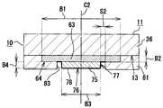
도 1에 나타내어지는 바와 같이, 본 실시형태의 배선기판(10)은 IC칩 탑재용의 배선기판이다. 배선기판(10)을 구성하는 기판 본체(11)는 기판 주면(12, 도 1에서는 상면) 및 기판 이면(13, 도 1에서는 하면)을 가지는 대략 직사각형 판 형상을 이루고 있다. 기판 본체(11)는 대략 직사각형 판 형상의 코어 기판(21)과, 코어 기판(21)의 코어 주면(22) 위에 형성되는 주면측 빌드업 층(31)과, 코어 기판(21)의 코어 이면(23) 위에 형성되는 이면측 빌드업 층(32)으로 이루어진다.As shown in Fig. 1, the
본 실시형태의 코어 기판(21)은 세로 25㎜×가로 25㎜×두께 1.0㎜인 평면시 대략 직사각형 판 형상이다. 코어 기판(21)은 평면 방향(XY 방향)에 있어서의 열팽창계수가 10∼30ppm/℃(구체적으로는 18ppm/℃)로 되어 있다. 또한, 코어 기판(21)의 열팽창계수는 0℃∼유리전이온도(Tg) 사이의 측정값의 평균값을 말한다. 이 코어 기판(21)에 있어서의 복수 개소에는 스루홀 도체(24)가 형성되어 있다. 상기 스루홀 도체(24)는 코어 기판(21)의 코어 주면(22)측과 코어 이면(23)측을 접속 도통하고 있다. 또한 스루홀 도체(24)의 내부는, 예를 들면 에폭시 수지 등의 폐색체 (25)로 매립되어 있다. 또, 코어 기판(21)의 코어 주면(22) 및 코어 이면(23)에는 구리로 이루어지는 도체층(41)이 패턴 형성되어 있으며, 각 도체층(41)은 스루홀 도체(24)에 전기적으로 접속되어 있다.The
도 1에 나타내어지는 바와 같이, 주면측 빌드업 층(31)은 열경화성 수지(에폭시 수지)로 이루어지는 2층의 수지절연층(33, 35)과, 구리로 이루어지는 도체층 (42)을 교호로 적층한 구조를 갖고 있다. 본 실시형태에 있어서, 수지절연층(33, 35)의 열팽창계수는 10∼60ppm/℃ 정도(구체적으로는 30ppm/℃ 정도)로 되어 있다. 또한, 수지절연층(33, 35)의 열팽창계수는 30℃∼유리전이온도(Tg) 사이의 측정값의 평균값을 말한다. 또, 제 2 층의 수지절연층(35)의 표면 위에 있어서의 복수 개소에는 단자 패드(44)가 어레이 형상으로 형성되어 있다. 또한, 수지절연층(35)의 표면은 솔더 레지스트(37)에 의해서 거의 전체적으로 덮여 있다. 솔더 레지스트 (37)의 소정 개소에는 단자 패드(44)를 노출시키는 개구부(46)가 형성되어 있다. 단자 패드(44)의 표면 위에는 복수의 솔더 범프(45)가 배치 설치되어 있다. 각 솔더 범프(45)는 직사각형 평판 형상을 이루는 IC칩(51)의 면접속단자(52)에 전기적으로 접속되어 있다. 또한, 각 단자 패드(44) 및 각 솔더 범프(45)로 이루어지는 영역은 IC칩(51)을 탑재 가능한 IC칩 탑재영역(53)이다. IC칩 탑재영역(53)은 주면측 빌드업 층(31)의 표면에 설정되어 있다. 또, 수지절연층(33, 35) 내에는 각각 비아 도체(43, 47)가 설치되어 있다. 이들의 비아 도체(43, 47)는 도체층(42) 및 단자 패드(44)를 상호 전기적으로 접속하고 있다.1, the main surface side build-
도 1에 나타내어지는 바와 같이, 이면측 빌드업 층(32)은 상기한 주면측 빌드업 층(31)과 거의 같은 구조를 갖고 있다. 즉, 이면측 빌드업 층(32)은 열경화성 수지(에폭시 수지)로 이루어지는 2층의 수지절연층(34, 36)과, 도체층(42)을 교호로 적층한 구조를 갖고 있으며, 수지절연층(34, 36)의 열팽창계수가 10∼60ppm/℃ 정도(구체적으로는 30ppm/℃ 정도)로 되어 있다.As shown in Fig. 1, the backside build-
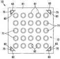
도 1∼도 3에 나타내어지는 바와 같이, 배선기판(10)의 기판 이면(13) 위[제 2 층의 수지절연층(36)의 하면 위]에는 평면시 원형 형상을 이루는 제 1 패드(61)가 기판 이면(13)의 면 방향을 따라서 가로 세로로 복수 배열되어 있다. 각 제 1 패드(61)는 비아 도체(43)를 통하여 도체층(42)에 전기적으로 접속되도록 되어 있다. 또한, 도 3에 나타내어지는 바와 같이, 각 제 1 패드(61)의 외경(A1)은 비아 도체(43)의 외경(본 실시형태에서는 50㎛ 이상 100㎛ 이하)보다도 크게(본 실시형태에서는 300㎛ 이상 700㎛ 이하) 설정되어 있다. 또, 본 실시형태에 있어서의 각 제 1 패드(61)의 두께(A2)는 10㎛ 이상 30㎛ 이하로 설정되어 있다.As shown in Figs. 1 to 3, on the
도 1∼도 3에 나타내어지는 바와 같이, 각 제 1 패드(61)의 하면(62, 표면)의 중앙 부분에는 평면시 원형 형상을 이루는 제 1 볼록부(71)가 고정되어 있다. 제 1 볼록부(71)는 제 1 패드(61)와는 별체로 형성되어 있다. 또, 제 1 볼록부(71)는 기판 이면(13)측에 있어서 복수 존재하고 있으며, 1개의 제 1 패드(61)에 대해서 1개소씩 배치되어 있다. 따라서, 제 1 볼록부(71)의 수는 제 1 패드(61)의 수와 동일하게 되어 있다. 또한, 제 1 볼록부(71)는 제 1 패드(61)와 같은 도전성 재료인 구리를 주체로 하여 형성된 구리 포스트이다.As shown in Figs. 1 to 3, a first
또, 도 3에 나타내어지는 바와 같이, 각 제 1 볼록부(71)는 선단면(72) 및 외측면(73)을 가지는 단면 대략 직사각형 형상을 이루고 있다. 그리고 제 1 볼록부 (71)는 선단면(72)과 외측면(73)의 경계 부분이 둥그스름한 형상을 이루고 있다. 또한, 각 제 1 볼록부(71)의 외경(A3)은 제 1 패드(61)의 외경(A1, 300㎛ 이상 700㎛ 이하)보다도 작게 설정되고, 본 실시형태에서는 200㎛ 이상 600㎛ 이하로 설정되어 있다. 또, 제 1 볼록부(71)는 제 1 패드(61)의 하면(62)에서 선단면(72)까지의 높이(A4)가 제 1 패드(61)의 두께(A2, 10㎛ 이상 30㎛ 이하)보다도 크게 설정되어 있으며, 본 실시형태에서는 15㎛ 이상 35㎛ 이하로 설정되어 있다. 그리고 제 1 볼록부(71)의 중심축은 제 1 패드(61)의 중심축(C1)과 일치하고 있다. 또한, 「중심축(C1)」이란, 평면시로 제 1 패드(61)의 중심이 되는 개소를 통과하는 축선을 말한다.3, each of the first
또한, 제 1 패드(61)의 표면[하면(62)]의 일부 및 제 1 볼록부(71)의 표면[선단면(72) 및 외측면(73)]은 도금층(74)에 의해서 연속적으로 덮여 있다. 도금층 (74)은 니켈층, 팔라듐층 및 금층에 의해서 구성되어 있다. 니켈층은 제 1 패드 (61)의 표면의 일부 및 제 1 볼록부(71)의 표면을 무전해 니켈 도금으로 피복함으로써 형성된 도금층이다. 팔라듐층은 니켈층의 표면을 무전해 팔라듐 도금으로 피복함으로써 형성된 도금층이다. 금층은 니켈층의 표면을 무전해 금 도금으로 피복함으로써 형성된 도금층이다. 또, 제 1 패드(61) 및 제 1 볼록부(71)는 도금층 등의 개재물을 통하는 일없이 직접 접속되어 있다. 또한, 본 실시형태의 도금층(74)은 니켈층, 팔라듐층 및 금층으로 이루어지는 구조를 갖고 있지만, 층 구조는 적절히 변경하는 것이 가능하다.A part of the surface (lower surface 62) of the
도 2, 도 4에 나타내어지는 바와 같이, 배선기판(10)의 기판 이면(13) 위에 있어서의 외주부(4코너)에는 평면시 삼각형 형상을 이루는 제 2 패드(63)가 각각 배치되어 있다. 또한, 도 4에 나타내어지는 바와 같이, 각 제 2 패드(63)의 외경 (B1, 최대 직경)은 각 제 1 패드(61)의 외경(A1, 300㎛ 이상 700㎛ 이하)보다도 크게 설정되고, 본 실시형태에서는 400㎛ 이상 800㎛ 이하로 설정되어 있다. 또, 본 실시형태에 있어서의 각 제 2 패드(63)의 두께(B2)는 10㎛ 이상 30㎛ 이하로 설정되어 있다.As shown in Figs. 2 and 4,
도 2, 도 4에 나타내어지는 바와 같이, 각 제 2 패드(63)의 하면(64, 표면)의 중앙 부분에는 평면시 삼각형 형상을 이루는 제 2 볼록부(75)가 고정되어 있다. 제 2 볼록부(75)는 제 2 패드(63)와는 별체로 형성되어 있다. 또, 제 2 볼록부(75)는 기판 이면(13)측에 있어서 복수 존재하고 있으며, 1개의 제 2 패드(63)에 대해서 1개소씩 배치되어 있다. 따라서, 제 2 볼록부(75)의 수는 제 2 패드(63)의 수와 동일하게 되어 있다. 또한, 제 2 볼록부(75)는 제 2 패드(63)와 같은 도전성 재료인 구리를 주체로 하여 형성된 구리 포스트이다.As shown in Figs. 2 and 4, a second
또, 도 4에 나타내어지는 바와 같이, 각 제 2 볼록부(75)는 선단면(76) 및 외측면(77)을 가지는 단면 대략 직사각형 형상을 이루고 있다. 그리고 제 2 볼록부 (75)는 선단면(76)과 외측면(77)의 경계 부분이 둥그스름한 형상을 이루고 있다. 또한, 각 제 2 볼록부(75)의 외경(B3, 최대 직경)은 제 2 패드(63)의 외경(B1, 400㎛ 이상 800㎛ 이하)보다도 작게 설정되고, 본 실시형태에서는 200㎛ 이상 600㎛ 이하로 설정되어 있다. 또, 제 2 볼록부(75)는 제 2 패드(63)의 하면(64)에서 선단면(76)까지의 높이(B4)가 제 2 패드(63)의 두께(B2, 10㎛ 이상 30㎛ 이하)보다도 크고, 또한, 제 1 볼록부(71)의 높이(A4)와 동일하게 설정되어 있으며, 본 실시형태에서는 15㎛ 이상 35㎛ 이하로 설정되어 있다. 그리고 제 2 볼록부(75)의 중심축은 제 2 패드(63)의 중심축(C2)과 일치하고 있다. 또한, 「중심축(C2)」이란, 평면시로 제 2 패드(63)의 중심이 되는 개소를 통과하는 축선을 말한다.4, each of the second
또한, 제 2 패드(63)의 표면[하면(64)]의 일부 및 제 2 볼록부(75)의 표면[선단면(76) 및 외측면(77)]은 도금층(78)에 의해서 연속적으로 덮여 있다. 도금층 (78)은 니켈층, 팔라듐층 및 금층에 의해서 구성되고, 도금층(74)과 같은 층 구조를 갖고 있다. 또, 제 2 패드(63) 및 제 2 볼록부(75)는 도금층 등의 개재물을 통하는 일없이 직접 접속되어 있다. 또한, 본 실시형태의 도금층(78)은 니켈층, 팔라듐층 및 금층으로 이루어지는 구조를 갖고 있지만, 층 구조는 적절히 변경하는 것이 가능하다.A part of the surface (lower surface 64) of the
도 1∼도 4에 나타내어지는 바와 같이, 배선기판(10)의 기판 이면[13, 수지절연층(36)의 하면]은 솔더 레지스트(81)에 의해서 거의 전체적으로 덮여 있다. 이 솔더 레지스트(81)에는 제 1 패드(61) 및 제 1 볼록부(71)를 노출시키는 복수의 제 1 개구부(82)와, 제 2 패드(63) 및 제 2 볼록부(75)를 노출시키는 복수의 제 2 개구부(83)가 형성되어 있다.As shown in Figs. 1 to 4, the
또한, 제 1 개구부(82)는 평면시 원형 형상을 이루고, 내경이 300㎛ 이상 700㎛ 이하로 설정되어 있다. 따라서, 제 1 개구부(82)의 평면시의 형상은 제 1 볼록부(71)의 평면시의 형상과 상사형을 이루고 있다. 또, 제 1 볼록부(71)는 외측면 (73)이 제 1 개구부(82)의 내측면과 마주 보도록 제 1 개구부(82) 내에 배치됨과 아울러, 외측면(73)이 제 1 개구부(82)의 내측면에 접근하도록 제 1 개구부(82) 내에 배치되어 있다. 그리고 제 1 볼록부(71)는 외측면(73)과 제 1 개구부(82) 내측면의 간극(S1)의 크기(본 실시형태에서는 50㎛ 정도)가 균일하게 되어 있다. 또, 제 1 볼록부(71)의 높이(A4, 15㎛ 이상 35㎛ 이하)는 제 1 개구부(82)의 깊이(본 실시형태에서는 20㎛ 이상 40㎛ 이하)보다도 작게 설정되어 있다.The
도 2, 도 4에 나타내어지는 바와 같이, 제 2 개구부(83)는 평면시 삼각형 형상을 이루고, 내경(최대 직경)이 400㎛ 이상 800㎛ 이하로 설정되어 있다. 따라서, 제 2 개구부(83)의 평면시의 형상은 제 2 볼록부(75)의 평면시의 형상과 상사형을 이루고 있다. 또, 제 2 볼록부(75)는 외측면(77)이 제 2 개구부(83)의 내측면과 마주 보도록 제 2 개구부(83) 내에 배치됨과 아울러, 외측면(77)이 제 2 개구부(83)의 내측면에 접근하도록 제 2 개구부(83) 내에 배치되어 있다. 그리고 제 2 볼록부 (75)는 외측면(77)과 제 2 개구부(83)의 내측면의 간극(S2)의 크기(본 실시형태에서는 50㎛ 정도)가 균일하게 되어 있다. 또, 제 2 볼록부(75)의 높이(B4, 15㎛ 이상 35㎛ 이하)는 제 2 개구부(83)의 깊이(본 실시형태에서는 20㎛ 이상 40㎛ 이하)보다도 작게 설정되어 있다.As shown in Figs. 2 and 4, the
또한, 각 볼록부(71, 75) 중, 각 제 1 볼록부(71)는 마더보드(91) 접속용의 볼록부이며, 각 제 2 볼록부(75)는 위치맞춤용 마크가 되는 볼록부이다. 제 2 볼록부(75)의 평면시의 형상(본 실시형태에서는 평면시 삼각형 형상)은 제 1 볼록부 (71)의 평면시의 형상(본 실시형태에서는 평면시 원형 형상)과는 다르다. 이 위치맞춤용 마크는 제 2 볼록부(75)의 선단면(72)의 외주연이나, 제 1 개구부(82)의 개구단 가장자리를 도시하지 않는 검출장치로 검출함으로써 인식된다.Each of the first
도 1, 도 3에 나타내어지는 바와 같이, 제 1 패드(61)의 표면 위에는 마더보드(91)와의 접속에 이용되는 솔더 범프(84)가 형성되어 있다. 상세히 서술하면, 각 개구부(82, 83) 중, 제 1 개구부(82) 내에 배치된 제 1 볼록부(71)의 표면[선단면 (72) 및 외측면(73)] 위에, 솔더 범프(84)가 형성되어 있다. 솔더 범프(84)는 제 1 패드(61)의 하면(62)에 있어서 제 1 개구부(82) 내로 노출된 영역을 덮음과 아울러, 제 1 볼록부(71)의 표면 전체를 덮고 있다. 이로 인해, 제 1 패드(61) 및 제 1 볼록부(71)는 솔더 범프(84)에 덮여 보이지 않게 되어 있다. 솔더 범프(84)의 높이는 제 1 볼록부(71)의 높이(A4, 15㎛ 이상 35㎛ 이하)보다도 높고, 본 실시형태에서는 300㎛ 이상 700㎛ 이하로 설정되어 있다. 또한, 본 실시형태의 솔더 범프 (84)는 무연 솔더인 Sn-Ag계 솔더로 이루어져 있다. 그리고 도 3에 나타내어지는 바와 같이, 각 제 1 패드(61)는 솔더 범프(84)를 통하여 마더보드(91)측의 단자 (92)에 접속되도록 되어 있다. 즉, 솔더 범프(84)는 마더보드(91)측의 단자(92)와의 전기적인 접속에 이용되는, 이른바 BGA 범프이다.As shown in Figs. 1 and 3, on the surface of the
다음에, 배선기판(10)의 제조방법에 대해서 설명한다.Next, a method of manufacturing the
우선, 기판 본체(11)를 준비하는 기판준비공정을 실시한다. 구체적으로는, 우선, 유리 에폭시로 이루어지는 기재의 양면에 구리박이 첩부된 동장적층판을 준비한다. 그리고 드릴기를 이용하여 천공 가공을 실시하여 동장적층판의 표리면을 관통하는 관통구멍을 소정 위치에 미리 형성하여 둔다. 그리고 관통구멍의 내면에 대해서 무전해 구리 도금 및 전해 구리 도금을 실시함으로써, 관통구멍 내에 스루홀 도체(24)를 형성한다. 그 후, 스루홀 도체(24)의 공동부(空洞部)를 절연수지재료(에폭시 수지)로 메워서 폐색체(25)를 형성한다.First, a substrate preparing process for preparing the substrate
또한, 무전해 구리 도금 및 전해 구리 도금을 실시함으로써, 폐색체(25)의 노출부분을 포함하는 동장적층판의 표면에 구리도금층을 형성한 후, 그 구리 도금 구리 및 구리박을 예를 들면 서브트랙티브법에 따라서 패터닝한다. 그 결과, 도체층(41) 및 스루홀 도체(24)가 형성된 코어 기판(21)의 중간제품을 얻는다. 또한, 코어 기판(21)의 중간제품이란, 코어 기판(21)이 되어야 할 영역이 평면 방향을 따라서 가로 세로로 복수 배치된 다수개 취득용 코어 기판이다.Further, by performing electroless copper plating and electrolytic copper plating, a copper plating layer is formed on the surface of the copper clad laminate including the exposed portion of the occluding
다음에, 코어 기판(21)의 코어 주면(22) 위에 주면측 빌드업 층(31)을 형성함과 아울러, 코어 기판(21)의 코어 이면(23) 위에 이면측 빌드업 층(32)을 형성한다. 구체적으로 말하면, 우선, 코어 주면(22) 위에 열경화성 에폭시 수지를 피착(被着, 첩부)함으로써, 수지절연층(33)을 형성한다. 또, 코어 이면(23) 위에 열경화성 에폭시 수지를 피착(첩부)함으로써, 수지절연층(34)을 형성한다. 또한, 열경화성 에폭시 수지를 피착하는 대신에, 감광성 에폭시 수지나 절연 수지나 액정폴리머(LCP: Liquid Crystalline Polymer)를 피착해도 좋다.Next, the main surface side build-
또한, YAG 레이저 또는 탄산가스레이저를 이용하여 레이저 천공 가공을 실시하고, 비아 도체(47)가 형성되어야 할 위치에 비아 구멍을 형성한다. 구체적으로는, 수지절연층(33)을 관통하는 비아 구멍을 형성하고, 도체층(41)의 표면을 노출시킨다. 또, 수지절연층(34)을 관통하는 비아 구멍을 형성하고, 도체층(41)의 표면을 노출시킨다. 다음에, 종래 공지의 수법에 따라서 전해 구리 도금을 실시하여 비아 구멍의 내부에 비아 도체(47)를 형성함과 아울러, 수지절연층(33, 34) 위에 도체층(42)을 형성한다.Laser drilling is also performed using a YAG laser or a carbon dioxide gas laser to form a via hole at a position where the via
다음에, 수지절연층(33, 34) 위에 열경화성 에폭시 수지를 피착하여 수지절연층(35, 36)을 형성한다. 또한, 열경화성 에폭시 수지를 피착하는 대신에, 감광성 에폭시 수지나 절연 수지나 액정 폴리머를 피착해도 좋다. 이 경우, 레이저 가공기 등에 의해, 수지절연층(35)에 있어서 비아 도체(43)가 형성되어야 할 위치에 비아 구멍이 형성된다. 다음에, 종래 공지의 수법에 따라서 전해 구리 도금을 실시하여 수지절연층(35)의 비아 구멍 내에 비아 도체(43)를 형성함과 아울러, 수지절연층 (35) 위에 단자 패드(44)를 형성한다. 또한, 이 시점에서 기판 본체(11)가 완성된다.Next, thermosetting epoxy resin is adhered to the
계속되는 패드 형성공정에서는 기판 이면(13)을 가지는 최외층의 수지절연층 (36) 위에 대해서 도금을 실시함으로써, 기판 이면(13) 위에 패드(61, 63)를 형성한다(도 5 참조). 본 실시형태에서는 세미 애디티브법을 실시함으로써, 수지절연층 (36) 위에 패드(61, 63)를 패턴 형성한다. 구체적으로 말하면, 우선, 레이저 가공을 시행함으로써 수지절연층(36)의 소정의 위치에 비아 구멍을 형성하고, 이어서 각 비아 구멍 내의 스미어를 처리하는 디스미어처리를 실시한다. 다음에, 수지절연층(36)의 표면에 대해서 무전해 구리 도금을 실시한 후, 수지절연층(36) 위에 드라이 필름을 래미네이트하여 제 1 도금 레지스트(도시생략)를 형성한다. 또한, 제 1 도금 레지스트에 대해서 레이저 가공기를 이용하여 레이저 가공을 실시한다. 그 결과, 수지절연층(36)에 있어서 비아 구멍과 연통하는 위치에, 내경이 비아 구멍의 외경보다도 크게 설정된 제 1 개구부가 형성됨과 아울러, 수지절연층(36)에 있어서 비아 구멍과 연통하지 않는 위치에 제 2 개구부가 형성된다. 그리고 전해 구리 도금을 실시하여 각 비아 구멍 내에 비아 도체(43)를 형성함과 아울러, 제 1 개구부를 통하여 노출된 수지절연층(36)의 상면[기판 이면(13)] 및 제 1 개구부를 통하여 노출된 비아 도체(43)의 상면에 대해서, 구리(구리층)를 주체로 하는 제 1 패드 (61)를 형성한다. 또, 제 2 개구부를 통하여 노출된 수지절연층(36)의 상면[기판 이면(13)]에 대해서, 구리(구리층)를 주체로 하는 제 2 패드(63)를 형성한다. 그 후, 제 1 도금 레지스트를 박리함과 아울러, 불필요한 무전해 구리 도금층을 제거 한다. 또한, 본 실시형태에 있어서의 구리층의 두께는 10㎛ 이상 30㎛ 이하로 설정되어 있다. 본 실시형태의 구리층은 도금에 의해서 형성되어 있지만, 스퍼터법, CVD 등의 다른 방법에 의해 형성하는 것도 가능하다. 그러나, 특히 구리층에 있어서 필요한 높이(10㎛ 이상 30㎛ 이하)를 얻기 위해서는, 도금에 의해서 형성되는 것이 바람직하다.In the subsequent pad forming step, plating is performed on the
계속되는 솔더 레지스트 형성공정에서는 패드(61, 63)가 형성된 수지절연층 (36) 위에 감광성 에폭시 수지를 도포하여 경화시킴으로써, 기판 이면(13)을 덮도록 솔더 레지스트(81)를 형성한다(도 6 참조). 다음에, 소정의 마스크를 배치한 상태에서 노광 및 현상을 실시하여 솔더 레지스트(81)에 개구부(82, 83)를 패터닝한다(도 6 참조).The solder resist 81 is formed so as to cover the
계속되는 볼록부 형성공정에서는 각 패드(61, 63)에 대해서 도금을 실시함으로써, 각 패드(61, 63)의 하면(62, 64)에 볼록부(71, 75)를 형성한다(도 7 참조). 구체적으로 말하면, 우선, 솔더 레지스트(81)의 표면에 드라이 필름을 래미네이트하여 제 2 도금 레지스트(도시생략)를 형성한다. 다음에, 제 2 도금 레지스트에 대해서 레이저 가공기를 이용한 레이저 가공을 실시한다. 그 결과, 패드(61, 63)의 하면(62, 64)의 중앙부를 노출시키는 개구부가 형성된다. 그리고 개구부를 통하여 노출된 하면(62, 64)의 중앙부에 대해서 전해 구리 도금을 실시한다. 이 시점에서 구리(구리층)를 주체로 하는 볼록부(71, 75)가 형성된다. 그 후, 제 2 도금 레지스트를 박리한다. 여기서, 볼록부(71, 75)를 구성하는 구리층의 두께는 15㎛ 이상 35㎛ 이하로 설정되어 있다. 또한, 본 실시형태에서는 구리층을 전해 도금에 의해서 형성하고 있지만, 무전해 도금, 스퍼터법, CVD 등의 다른 방법에 의해 형성하는 것도 가능하다. 그러나, 특히 구리층에 있어서 필요한 높이(15㎛ 이상 35㎛ 이하)를 얻기 위해서는, 도금에 의해서 형성되는 것이 바람직하다.The
그 후, 무전해 니켈 도금을 실시하여, 패드(61, 63)의 표면[하면(62, 64)]과 볼록부(71, 75)의 표면[(선단면(72, 76) 및 외측면(73, 77)]에 대해서 니켈층을 형성한다. 또한, 무전해 팔라듐 도금을 실시하여 니켈층 위에 팔라듐층을 형성한다. 그리고 무전해 금 도금을 실시하여 팔라듐층 위에 금층을 형성한다. 여기서, 니켈층, 팔라듐층 및 금층의 두께는 0.01㎛ 이상 15㎛ 이하로 설정되어 있다. 또한, 본 실시형태의 니켈층, 팔라듐층 및 금층은 도금에 의해서 형성되어 있지만, 스퍼터법, CVD 등의 다른 방법에 의해 형성하는 것도 가능하다.Thereafter, electroless nickel plating is carried out so that the surfaces (
계속되는 솔더 범프 형성공정에서는 배선기판(10)의 기판 이면(13)측에 형성되어 있는 복수의 제 1 패드(61) 위에 솔더 범프(84)를 형성한다. 구체적으로는, 도시하지 않는 솔더볼 탑재장치를 이용하여 각 제 1 패드(61) 위에 솔더볼을 배치한 후, 솔더볼을 소정의 온도로 가열하여 가열 용융(리플로우)함으로써, 각 제 1 패드(61) 위에 솔더 범프(84)를 형성한다. 또, 배선기판(10)의 기판 주면(12)측에 형성되어 있는 복수의 단자 패드(44) 위에 솔더 범프(45)를 형성한다. 구체적으로는, 솔더볼 탑재장치를 이용하여 각 단자 패드(44) 위에 솔더볼을 배치한 후, 솔더볼을 소정의 온도로 가열하여 가열 용융(리플로우)함으로써, 각 단자 패드(44) 위에 솔더 범프(45)를 형성한다. 또한, 이 시점에서 배선기판(10)의 중간제품이 완성된다.In the succeeding solder bump forming process, solder bumps 84 are formed on the plurality of
그 후, 종래 주지의 절단장치 등을 이용하여 배선기판(10)의 중간제품을 분할한다. 그 결과, 제품부끼리가 분할되어 개개의 제품인 배선기판(10)이 다수 개 동시에 얻어진다(도 1 참조).Thereafter, the intermediate product of the
또한, IC칩 탑재공정을 실시한다. 구체적으로 말하면, 우선, 배선기판(10)의 기판 주면(12)측에 IC칩(51)을 얹어 놓는다. 이때, IC칩(51)의 바닥면측에 배치된 면접속단자(52)를 배선기판(10)측에 배치된 솔더 범프(45) 위에 얹어 놓도록 한다. 그리고 230℃∼260℃정도의 온도로 가열하여 각 솔더 범프(45)를 가열 용융(리플로우)함으로써, 단자 패드(44)가 면접속단자(52)에 대해서 플립 칩 접속되어 배선기판(10)에 IC칩(51)이 탑재된다(도 1 참조).Further, an IC chip mounting step is performed. Specifically, first, the
따라서, 본 실시형태에 따르면 이하의 효과를 얻을 수 있다.Therefore, according to the present embodiment, the following effects can be obtained.
(1) 본 실시형태의 배선기판(10)에서는 솔더 범프(84)에 크랙(100, 도 3 참조)이 발생하고, 발생한 크랙(100)이 솔더 범프(84)와 제 1 패드(61)의 계면을 따라서 진행되었다고 해도, 크랙(100)이 제 1 볼록부(71)에 도달함으로써 그 진행이 확실하게 억제된다. 그 결과, 솔더 범프(84)에 의해서 구성되는 전기 경로의 단선을 방지할 수 있기 때문에, 제조되는 배선기판(10)의 신뢰성을 향상시키는 것이 가능하게 된다.(1) In the
(2) 본 실시형태에서는 제 1 패드(61)의 하면(62)의 일부에 제 1 볼록부(71)가 고정되고, 전체적으로 볼록 형상을 이루고 있다. 그러므로, 제 1 패드(61)의 표면[하면(62)] 및 제 1 볼록부(71)의 표면[선단면(72) 및 외측면(73)]을 덮는 솔더 범프(84)를 형성하면, 솔더 범프(84) 내에 제 1 볼록부(71)가 끼워 넣어진 상태가 된다. 그 결과, 제 1 패드(61) 및 제 1 볼록부(71)는 솔더 범프(84)와의 접촉면적이 확보된다. 따라서, 제 1 패드(61)의 표면과 솔더 범프(84)의 밀착 강도나, 제 1 볼록부(71)의 표면과 솔더 범프(84)의 밀착 강도를 높게 할 수 있으며, 나아가서는, 개개의 제 1 패드(61)와 마더보드(91)의 접속 불량을 방지할 수 있다. 즉, 마더보드(91)와의 접속에 적합한 제 1 패드(61) 및 제 1 볼록부(71)를 구비함으로써, 배선기판(10)의 신뢰성을 더한층 향상시킬 수 있다.(2) In the present embodiment, the first
(3) 본 실시형태에서는 제 1 볼록부(71)에 있어서의 제 1 패드(61)의 하면 (62)에서 선단면(72)까지의 높이(A4)가 제 1 개구부(82)의 깊이보다도 작게 설정되어 있다. 그 결과, 솔더 범프 형성공정에 있어서, 솔더 범프(84)가 되는 솔더볼을 제 1 개구부(82) 내에 확실하게 배치할 수 있다.(3) In this embodiment, the height A4 from the
또한, 본 실시형태를 이하와 같이 변경해도 좋다.The present embodiment may be modified as follows.
ㆍ상기 실시형태에서는 마더보드(91) 접속용의 제 1 볼록부(71)의 평면시의 형상(평면시 원형 형상)과 위치맞춤용 마크가 되는 제 2 볼록부(75)의 평면시의 형상(평면시 삼각형 형상)이 서로 다르지만, 볼록부(71, 75)의 평면시의 형상을 서로 동일한 형상으로 해도 좋다.(The circular shape in plan view) of the first
ㆍ상기 실시형태에서는 1개의 패드(61, 63)에 대해서 1개의 볼록부(71, 75)를 형성하고 있었지만, 이것에 한정되는 것은 아니고, 2개 이상의 볼록부를 형성해도 좋다.In the above embodiment, one
ㆍ상기 실시형태의 볼록부(71, 75)는 구리 도금에 의해서 형성된 도체(구리 포스트)이었지만, 구리 페이스트를 인쇄함으로써 형성된 도체라도 좋다.The
ㆍ상기 실시형태에서는 패드(61, 63) 및 볼록부(71, 75)를 피복하는 도금층 (74, 78)이 니켈층, 팔라듐층 및 금층으로 이루어지는 도금층이었지만, 구리층 이외의 도금층이면 좋고, 예를 들면, 니켈층 및 금층 등으로 이루어지는 다른 도금층으로 변경해도 좋다.In the above embodiment, the plating layers 74 and 78 covering the
ㆍ상기 실시형태의 솔더 범프 형성공정에서는 제 1 패드(61) 위에 배치한 솔더볼을 가열 용융(리플로우)시킴으로써, 솔더 범프(84)를 형성하고 있었다. 그러나, 제 1 패드(61) 위에 인쇄된 솔더 페이스트를 가열 용융시킴으로써, 솔더 범프를 형성하도록 해도 좋다.In the solder bump forming step of the embodiment, the solder bumps 84 are formed by heating and melting (reflowing) the solder balls disposed on the
다음에, 상기한 실시형태에 의해서 파악되는 기술적 사상을 이하에 열거한다.Next, technical ideas that are grasped by the above embodiment will be listed below.
(1) 상기 수단 1에 있어서, 상기 패드 표면의 적어도 일부, 상기 선단면 및 상기 외측면은 도금층에 의해서 연속적으로 덮여 있으며, 상기 볼록부는 상기 도금층을 통하는 일없이, 상기 패드의 표면에 직접 접속되어 있는 것을 특징으로 하는 배선기판.(1) In the above-mentioned
(2) 상기 수단 1에 있어서, 상기 볼록부는 상기 기판 이면측에 있어서 복수 존재하고 있으며, 복수의 상기 볼록부의 적어도 일부는 위치맞춤용 마크이며, 상기 위치맞춤용 마크가 되는 상기 볼록부는 상기 기판 이면측에 있어서의 외주부에 위치하고 있는 것을 특징으로 하는 배선기판.(2) In the
(3) 상기 수단 1에 기재된 배선기판을 제조하는 방법으로서, 상기 기판 본체를 준비하는 기판준비공정과, 상기 기판 이면 위에 상기 복수의 패드를 형성하는 패드 형성공정과, 상기 기판 이면을 덮도록 상기 솔더 레지스트를 형성하는 솔더 레지스트 형성공정과, 상기 복수의 패드 표면의 일부에 상기 볼록부를 형성하는 볼록부 형성공정을 포함하는 것을 특징으로 하는 배선기판의 제조방법.
(3) A method for manufacturing a wiring board as described in the above-mentioned
10: 배선기판
11: 기판 본체
12: 기판 주면
13: 기판 이면
61: 패드로서의 제 1 패드
62, 64: 패드의 표면으로서의 하면
63: 패드로서의 제 2 패드
71: 볼록부로서의 제 1 볼록부
72, 76: 볼록부의 표면으로서의 선단면
73, 77: 볼록부의 표면으로서의 외측면
74, 78: 도금층
75: 볼록부로서의 제 2 볼록부
81: 솔더 레지스트
82: 개구부로서의 제 1 개구부
83: 개구부로서의 제 2 개구부
84: 솔더 범프
91: 마더보드
A4, B4: 패드의 표면에서 선단면까지의 높이
S1, S2: 볼록부의 외측면과 개구부의 내측면의 간극10: wiring board
11:
12: substrate main surface
13:
61: first pad as a pad
62, 64: the lower surface as the surface of the pad
63: second pad as pad
71: first convex portion as a convex portion
72, 76: front surface as the surface of convex portion
73, 77: outer surface as the surface of the convex portion
74, 78: Plated layer
75: second convex portion as a convex portion
81: Solder resist
82: first opening as an opening
83: second opening as an opening
84: Solder bump
91: Motherboard
A4, B4: Height from the surface of the pad to the end face
S1, S2: Clearance between the outer surface of the convex portion and the inner surface of the opening
Claims (8)
Translated fromKorean상기 기판 이면 위에 배치되고, 마더보드와의 접속에 이용되는 솔더 범프가 표면 위에 형성되는 것이 가능한 복수의 패드와,
상기 기판 이면을 덮음과 아울러, 상기 복수의 패드를 노출시키는 복수의 개구부가 형성된 솔더 레지스트를 구비하는 배선기판으로서,
상기 패드의 표면의 일부에 선단면 및 외측면을 가지는 볼록부가 형성되고,
상기 볼록부는,
상기 패드의 표면에서 상기 선단면까지의 높이가 상기 개구부의 깊이보다도 작게 설정되며,
상기 외측면이 상기 개구부의 내측면과 마주 보도록 상기 개구부 내에 배치되고,
평면측에서 보았을 때의 형상이 상기 개구부의 평면측에서 보았을 때의 형상과 상사형을 이루고 있는 것을 특징으로 하는 배선기판.
A substrate main body having a substrate main surface and a substrate back surface,
A plurality of pads disposed on the back surface of the substrate and capable of forming solder bumps on the surface to be used for connection with the mother board,
And a solder resist covering the back surface of the substrate and having a plurality of openings exposing the plurality of pads,
A convex portion having a front end surface and an outer surface is formed on a part of the surface of the pad,
The convex portion
The height from the surface of the pad to the end face is set to be smaller than the depth of the opening,
The outer surface being disposed in the opening so as to face the inner surface of the opening,
Wherein the shape when viewed from the plane side is in a top shape with respect to the shape when viewed from the plane side of the opening.
상기 볼록부는 상기 외측면이 상기 개구부의 내측면에 접근하도록 상기 개구부 내에 배치되어 있는 것을 특징으로 하는 배선기판.The method according to claim 1,
And the convex portion is disposed in the opening so that the outer surface approaches the inner surface of the opening.
상기 볼록부는 상기 외측면과 상기 개구부의 내측면의 간극의 크기가 균일한 것을 특징으로 하는 배선기판.
The method according to claim 1 or 2,
Wherein a size of a gap between the outer side surface and the inner side surface of the opening is uniform in the convex portion.
상기 볼록부는 상기 선단면과 상기 외측면의 경계 부분이 둥그스름한 형상을 이루고 있는 것을 특징으로 하는 배선기판.
The method according to any one of claims 1 to 3,
Wherein the convex portion has a rounded shape at a boundary portion between the front end face and the outer side face.
상기 패드의 표면의 적어도 일부, 상기 선단면 및 상기 외측면은 도금층에 의해서 연속적으로 덮여 있는 것을 특징으로 하는 배선기판.
The method according to any one of claims 1 to 4,
Wherein at least a part of the surface of the pad, the front end surface, and the outer surface are continuously covered with a plating layer.
상기 볼록부는 상기 기판 이면측에 있어서 복수 존재하고 있으며, 복수의 상기 볼록부의 적어도 일부는 위치맞춤용 마크인 것을 특징으로 하는 배선기판.
The method according to any one of claims 1 to 5,
Wherein a plurality of the convex portions are present on the back surface of the substrate, and at least a part of the plurality of convex portions is an alignment mark.
상기 위치맞춤용 마크의 평면측에서 보았을 때의 형상은 마더보드 접속용의 상기 볼록부의 평면측에서 보았을 때의 형상과는 다른 것을 특징으로 하는 배선기판.
The method of claim 6,
Wherein the shape of the alignment mark as viewed from the plane side is different from the shape as viewed from the plane side of the convex portion for motherboard connection.
상기 복수의 개구부 중 적어도 1개의 상기 개구부 내에 배치된 상기 볼록부의 표면 위에, 상기 솔더 범프가 형성되어 있는 것을 특징으로 하는 배선기판.
The method according to any one of claims 1 to 7,
Wherein the solder bump is formed on the surface of the convex portion disposed in at least one of the plurality of openings.
Applications Claiming Priority (3)
| Application Number | Priority Date | Filing Date | Title |
|---|---|---|---|
| JPJP-P-2013-063369 | 2013-03-26 | ||
| JP2013063369AJP2014192176A (en) | 2013-03-26 | 2013-03-26 | Wiring board |
| PCT/JP2013/007314WO2014155455A1 (en) | 2013-03-26 | 2013-12-12 | Wiring board |
Publications (1)
| Publication Number | Publication Date |
|---|---|
| KR20150130519Atrue KR20150130519A (en) | 2015-11-23 |
Family
ID=51622554
Family Applications (1)
| Application Number | Title | Priority Date | Filing Date |
|---|---|---|---|
| KR1020157029234ACeasedKR20150130519A (en) | 2013-03-26 | 2013-12-12 | Wiring board |
Country Status (6)
| Country | Link |
|---|---|
| US (1) | US20150357277A1 (en) |
| JP (1) | JP2014192176A (en) |
| KR (1) | KR20150130519A (en) |
| CN (1) | CN104956477A (en) |
| TW (1) | TW201503771A (en) |
| WO (1) | WO2014155455A1 (en) |
Cited By (4)
| Publication number | Priority date | Publication date | Assignee | Title |
|---|---|---|---|---|
| KR20200045589A (en)* | 2018-10-22 | 2020-05-06 | 삼성전자주식회사 | Printed circuit board and semiconductor package including the same |
| US11735510B2 (en) | 2020-12-16 | 2023-08-22 | Samsung Electro-Mechanics Co., Ltd. | Printed circuit board and electronic component package |
| KR20240160939A (en)* | 2023-05-03 | 2024-11-12 | 주식회사 심텍 | printed circuit board including chip connection copper post having electroless plated surface treatment layer |
| WO2025159536A1 (en)* | 2024-01-23 | 2025-07-31 | 엘지이노텍 주식회사 | Circuit board and semiconductor package comprising same |
Families Citing this family (20)
| Publication number | Priority date | Publication date | Assignee | Title |
|---|---|---|---|---|
| JP6123915B2 (en)* | 2014-02-07 | 2017-05-10 | 株式会社村田製作所 | Resin multilayer board |
| TWI554174B (en)* | 2014-11-04 | 2016-10-11 | 上海兆芯集成電路有限公司 | Circuit substrate and semiconductor substrate |
| JP6510349B2 (en)* | 2015-07-27 | 2019-05-08 | 京セラ株式会社 | Wiring board |
| JP2017098338A (en)* | 2015-11-19 | 2017-06-01 | 株式会社デンソー | Electronic device |
| JP2017152536A (en)* | 2016-02-24 | 2017-08-31 | イビデン株式会社 | Printed wiring board and manufacturing method thereof |
| JP2017199803A (en)* | 2016-04-27 | 2017-11-02 | 日立マクセル株式会社 | 3D molded circuit components |
| CN109156080B (en) | 2016-05-16 | 2021-10-08 | 株式会社村田制作所 | Ceramic electronic parts |
| JP2018018868A (en)* | 2016-07-26 | 2018-02-01 | イビデン株式会社 | Coil substrate and manufacturing method thereof |
| KR102373440B1 (en)* | 2017-03-17 | 2022-03-14 | 삼성디스플레이 주식회사 | Display panel and display apparatus comprising the same |
| US11444049B2 (en) | 2017-08-14 | 2022-09-13 | Sony Corporation | Electronic component module, method for producing the same, endoscopic apparatus, and mobile camera |
| US10978417B2 (en)* | 2019-04-29 | 2021-04-13 | Advanced Semiconductor Engineering, Inc. | Wiring structure and method for manufacturing the same |
| US11626336B2 (en)* | 2019-10-01 | 2023-04-11 | Qualcomm Incorporated | Package comprising a solder resist layer configured as a seating plane for a device |
| JP2021093417A (en)* | 2019-12-09 | 2021-06-17 | イビデン株式会社 | Print circuit board and manufacturing method of print circuit board |
| JP6754151B1 (en)* | 2020-02-18 | 2020-09-09 | 日本高純度化学株式会社 | Plating laminate |
| TWI731776B (en)* | 2020-08-26 | 2021-06-21 | 友達光電股份有限公司 | Electronic device |
| US20220069489A1 (en)* | 2020-08-28 | 2022-03-03 | Unimicron Technology Corp. | Circuit board structure and manufacturing method thereof |
| KR20220041430A (en)* | 2020-09-25 | 2022-04-01 | 삼성전자주식회사 | Fan out semiconductor package having a under-bump metal |
| US11744019B2 (en)* | 2020-11-18 | 2023-08-29 | Murata Manufacturing Co., Ltd. | Component mounted on circuit board |
| US20230070275A1 (en)* | 2021-09-09 | 2023-03-09 | Qualcomm Incorporated | Package comprising a substrate with a pad interconnect comprising a protrusion |
| WO2025120921A1 (en)* | 2023-12-08 | 2025-06-12 | 株式会社村田製作所 | Electronic module |
Family Cites Families (10)
| Publication number | Priority date | Publication date | Assignee | Title |
|---|---|---|---|---|
| KR100216839B1 (en)* | 1996-04-01 | 1999-09-01 | 김규현 | Solder Ball Land Metal Structure in BGA Semiconductor Package |
| JPH1074856A (en)* | 1996-08-29 | 1998-03-17 | Kyocera Corp | Package for storing semiconductor elements |
| JP3526508B2 (en)* | 1997-02-25 | 2004-05-17 | 京セラ株式会社 | Package for storing semiconductor elements |
| US6462414B1 (en)* | 1999-03-05 | 2002-10-08 | Altera Corporation | Integrated circuit package utilizing a conductive structure for interlocking a conductive ball to a ball pad |
| US6812718B1 (en)* | 1999-05-27 | 2004-11-02 | Nanonexus, Inc. | Massively parallel interface for electronic circuits |
| JP2001351946A (en)* | 2000-06-05 | 2001-12-21 | Mitsubishi Electric Corp | Semiconductor device |
| US6563905B1 (en)* | 2001-10-30 | 2003-05-13 | Qualcomm, Incorporated | Ball grid array X-ray orientation mark |
| US7446399B1 (en)* | 2004-08-04 | 2008-11-04 | Altera Corporation | Pad structures to improve board-level reliability of solder-on-pad BGA structures |
| JP5436963B2 (en)* | 2009-07-21 | 2014-03-05 | 新光電気工業株式会社 | Wiring substrate and semiconductor device |
| JP2012089710A (en)* | 2010-10-20 | 2012-05-10 | Toshiba Corp | Electronic quipment and flexible printed wiring board |
- 2013
- 2013-03-26JPJP2013063369Apatent/JP2014192176A/enactivePending
- 2013-12-12WOPCT/JP2013/007314patent/WO2014155455A1/enactiveApplication Filing
- 2013-12-12CNCN201380071660.2Apatent/CN104956477A/enactivePending
- 2013-12-12USUS14/762,185patent/US20150357277A1/ennot_activeAbandoned
- 2013-12-12KRKR1020157029234Apatent/KR20150130519A/ennot_activeCeased
- 2014
- 2014-03-20TWTW103110419Apatent/TW201503771A/enunknown
Cited By (4)
| Publication number | Priority date | Publication date | Assignee | Title |
|---|---|---|---|---|
| KR20200045589A (en)* | 2018-10-22 | 2020-05-06 | 삼성전자주식회사 | Printed circuit board and semiconductor package including the same |
| US11735510B2 (en) | 2020-12-16 | 2023-08-22 | Samsung Electro-Mechanics Co., Ltd. | Printed circuit board and electronic component package |
| KR20240160939A (en)* | 2023-05-03 | 2024-11-12 | 주식회사 심텍 | printed circuit board including chip connection copper post having electroless plated surface treatment layer |
| WO2025159536A1 (en)* | 2024-01-23 | 2025-07-31 | 엘지이노텍 주식회사 | Circuit board and semiconductor package comprising same |
Also Published As
| Publication number | Publication date |
|---|---|
| US20150357277A1 (en) | 2015-12-10 |
| CN104956477A (en) | 2015-09-30 |
| WO2014155455A1 (en) | 2014-10-02 |
| JP2014192176A (en) | 2014-10-06 |
| TW201503771A (en) | 2015-01-16 |
Similar Documents
| Publication | Publication Date | Title |
|---|---|---|
| KR20150130519A (en) | Wiring board | |
| TWI499012B (en) | Wiring substrate and method for manufacturing the same | |
| CN105228341B (en) | Printed circuit board, package substrate and its manufacturing method | |
| KR100595889B1 (en) | Semiconductor device having conduction part of upper and lower conductive layer and manufacturing method thereof | |
| KR101027711B1 (en) | Manufacturing method of multilayer wiring board | |
| US8780572B2 (en) | Printed circuit board having electronic component | |
| EP2592915A1 (en) | Laminated wiring board and manufacturing method for same | |
| JP2013149948A (en) | Wiring board and manufacturing method of the same | |
| KR20130045206A (en) | Wiring substrate and method of manufacturing the same | |
| US9510450B2 (en) | Printed wiring board and method for manufacturing the same | |
| KR20150092881A (en) | Pcb, package substrate and a manufacturing method thereof | |
| US20150364410A1 (en) | Circuit board, manufacturing method therefor, and pillar-shaped terminal for circuit board | |
| JP2013110329A (en) | Capacitor module built-in wiring board | |
| JP2013149810A (en) | Manufacturing method of multilayer wiring board | |
| JP2014192177A (en) | Wiring board | |
| CN107770946B (en) | Printed wiring board and method for manufacturing the same | |
| JP2016009740A (en) | Method for manufacturing wiring board | |
| KR20190068421A (en) | Wiring board and manufacturing method thereof | |
| KR20150009671A (en) | Printed circuit board substrate having metal post and the method of manufacturing the same | |
| KR101115461B1 (en) | Embedded PCB and Manufacturing method of the same | |
| KR101543031B1 (en) | Printed circuit board and method for manufacturing the same | |
| KR20110131040A (en) | Embedded printed circuit board and its manufacturing method | |
| TW201322837A (en) | Wiring substrate and method of manufacturing the same | |
| KR101241649B1 (en) | The printed circuit board and the method for manufacturing the same | |
| KR101115476B1 (en) | Embedded PCB and Manufacturing method of the same |
Legal Events
| Date | Code | Title | Description |
|---|---|---|---|
| A201 | Request for examination | ||
| PA0105 | International application | Patent event date:20151014 Patent event code:PA01051R01D Comment text:International Patent Application | |
| PA0201 | Request for examination | Patent event code:PA02012R01D Patent event date:20151014 Comment text:Request for Examination of Application | |
| PG1501 | Laying open of application | ||
| E902 | Notification of reason for refusal | ||
| PE0902 | Notice of grounds for rejection | Comment text:Notification of reason for refusal Patent event date:20160912 Patent event code:PE09021S01D | |
| E601 | Decision to refuse application | ||
| PE0601 | Decision on rejection of patent | Patent event date:20161116 Comment text:Decision to Refuse Application Patent event code:PE06012S01D Patent event date:20160912 Comment text:Notification of reason for refusal Patent event code:PE06011S01I |