KR20150124907A - Capacitive Type Touch Panel - Google Patents
Capacitive Type Touch PanelDownload PDFInfo
- Publication number
- KR20150124907A KR20150124907AKR1020150059456AKR20150059456AKR20150124907AKR 20150124907 AKR20150124907 AKR 20150124907AKR 1020150059456 AKR1020150059456 AKR 1020150059456AKR 20150059456 AKR20150059456 AKR 20150059456AKR 20150124907 AKR20150124907 AKR 20150124907A
- Authority
- KR
- South Korea
- Prior art keywords
- electrode
- mesh
- touch panel
- bridge
- diamond
- Prior art date
- Legal status (The legal status is an assumption and is not a legal conclusion. Google has not performed a legal analysis and makes no representation as to the accuracy of the status listed.)
- Granted
Links
Images


Classifications
- G—PHYSICS
- G06—COMPUTING OR CALCULATING; COUNTING
- G06F—ELECTRIC DIGITAL DATA PROCESSING
- G06F3/00—Input arrangements for transferring data to be processed into a form capable of being handled by the computer; Output arrangements for transferring data from processing unit to output unit, e.g. interface arrangements
- G06F3/01—Input arrangements or combined input and output arrangements for interaction between user and computer
- G06F3/03—Arrangements for converting the position or the displacement of a member into a coded form
- G06F3/041—Digitisers, e.g. for touch screens or touch pads, characterised by the transducing means
- G06F3/044—Digitisers, e.g. for touch screens or touch pads, characterised by the transducing means by capacitive means
- G—PHYSICS
- G06—COMPUTING OR CALCULATING; COUNTING
- G06F—ELECTRIC DIGITAL DATA PROCESSING
- G06F2203/00—Indexing scheme relating to G06F3/00 - G06F3/048
- G06F2203/041—Indexing scheme relating to G06F3/041 - G06F3/045
- G06F2203/04112—Electrode mesh in capacitive digitiser: electrode for touch sensing is formed of a mesh of very fine, normally metallic, interconnected lines that are almost invisible to see. This provides a quite large but transparent electrode surface, without need for ITO or similar transparent conductive material
Landscapes
- Engineering & Computer Science (AREA)
- General Engineering & Computer Science (AREA)
- Theoretical Computer Science (AREA)
- Position Input By Displaying (AREA)
- Human Computer Interaction (AREA)
- Physics & Mathematics (AREA)
- General Physics & Mathematics (AREA)
Abstract
Translated fromKoreanDescription
Translated fromKorean본 발명은, 단일층에 패터닝된 구동전극 및 감지전극을 포함하는 정전용량방식 터치패널에 관한 것이다.The present invention relates to a capacitive touch panel including a driving electrode and a sensing electrode patterned in a single layer.
터치패널장치는 전세계에서 모바일기기를 중심으로 수요량이 급격히 증가하고 있을 뿐만 아니라 기술적으로도 성장 및 안정화되고 있어, 다양한 중대형기기에서도 사용비중이 꾸준히 증가하고 있다. 터치패널장치는 오래전부터 PDA, 게임기, 네비게이션, POS, ATM기기 등에서 사용되어 왔지만, 전체 디스플레이산업에서 터치패널장치가 차지하는 비중이 크지 않았다. 하지만 소형 모바일기기를 시작으로 최근에는 다양한 모바일 멀티미디어기기 특히 스마트폰과 태블릿피씨(Tablet PCs) 등의 제품에 널리 적용되고 있다.The demand for touch panel devices has rapidly increased not only in mobile devices around the world but also in technological growth and stabilization. Touch panel devices have long been used in PDAs, game consoles, navigation systems, POS, and ATM devices. However, touch panel devices account for a small portion of the total display industry. However, recently, it has been widely applied to various mobile multimedia devices, especially smart phones and tablet PCs, starting with small mobile devices.
터치패널장치는 초기 낮은 원가구조와 세밀한 터치감으로 인해 주로 채택되었던 저항막방식에서 최근들어 터치감이 우수하고, 내구성, 광투과율 및 야외 시인성, 패널두께 등의 장점으로 인해 정전용량방식으로 대체되고 있다. 특히 10인치 이하 모바일기기에서 폭넓게 사용되고 있다.The touch panel device has recently been replaced by a capacitive type due to its excellent touch feeling and durability, light transmittance, outdoor visibility, panel thickness and the like in the resistive film type which is mainly adopted due to the initial low cost structure and fine touch feeling have. Especially, it is widely used in mobile devices less than 10 inches.
이러한 터치패널에는 투명전극이 사용되는데, 종래에는 ITO(Indium Tin Oxide; 인듐-주석산화물)나 폴리에틸렌디옥시티오펜/폴리스티렌술포네이트(PEDOT/PSS)와 같은 전도성 고분자를 이용하여 투명전극을 형성하였다. ITO의 경우, 소형기기에 사용하기에 적합한 전기전도도를 가지고 있으나, 대형 패널에 사용하기엔 부족한 부분이 있다. 전도성 고분자는 ITO를 대체하기 위하여 대두 된 물질로써, 유연성이 우수하며, 가공이 용이하다는 장점이 있으나 전기전도도가 떨어진다는 문제점이 있다.A transparent electrode is formed on the touch panel using a conductive polymer such as indium tin oxide (ITO) or polyethylene dioxythiophene / polystyrene sulfonate (PEDOT / PSS). In the case of ITO, it has an electrical conductivity suitable for use in small appliances, but it is insufficient for use in large panels. The conductive polymer is a material that has been developed to replace ITO, has excellent flexibility and is easy to process, but has a problem of low electrical conductivity.
상기와 같은 이유로 금속을 이용하여 투명전극을 형성하려는 연구가 진행되고 있는 바, 금속으로 형성된 투명전극은 ITO나 전도성 고분자에 비해 전기전도도가 훨씬 우수하며, 수급이 원활하다는 장점이 있다. 다만, 금속으로 전극을 형성 시, 불투명한 금속색상으로 인해 터치패널의 투명도가 문제된다.For the above reasons, studies have been made to form a transparent electrode using a metal. As a result, the transparent electrode formed of metal has a merit that the electric conductivity is much higher than that of the ITO or the conductive polymer, and the supply and discharge is smooth. However, when an electrode is formed of a metal, transparency of the touch panel is problematic due to opaque metal color.
정전용량방식 터치패널의 경우 이중층 터치패널 또는 단일층 터치패널로 나누어질 수 있다. 이중층 터치패널은 제1 전극패턴이 형성된 상부기판과 제2 전극패턴이 형성된 하부기판으로 이루어진 두개의 기판을 포함하며 이들은 서로 이격되며, 그 사이에 제1 전극패턴과 제2 전극패턴이 접촉하지 못하게 절연재가 삽입된다. 또한, 상부기판과 하부기판에는 전극패턴과 연결된 전극배선이 형성된다. 전극배선은 입력수단이 터치스크린에 접촉함에 따라 제1 전극패턴과 제2 전극패턴에서 발생하는 캐패시턴스 변화를 제어부에 전달한다.In case of capacitive touch panel, it can be divided into a double layer touch panel or a single layer touch panel. Layer touch panel includes two substrates composed of an upper substrate on which a first electrode pattern is formed and a lower substrate on which a second electrode pattern is formed and are separated from each other so that the first electrode pattern and the second electrode pattern are not in contact with each other, Insulation is inserted. Also, electrode wirings connected to the electrode patterns are formed on the upper substrate and the lower substrate. The electrode wiring transfers a capacitance change generated in the first electrode pattern and the second electrode pattern to the control unit as the input unit contacts the touch screen.
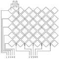
한편 단일층 터치패널은 하나의 기판 상에 서로 다른 방향으로 형성된 제 1 전극패턴과 제 2 전극패턴을 포함한다(도 1 참조)다. 즉, 도 1의 단일층 터치패널은 다수개의 마름모꼴(다이아몬드 형상)의 패턴들이 연결부를 통하여 연결되어 형성된 제 2전극과 다수개의 마름모꼴의 패턴들이 제 2 전극과의 교차부에서 서로 분리되어 브릿지에 의해 연결되어 형성된 제 1 전극으로 구성된다.On the other hand, the single-layer touch panel includes a first electrode pattern and a second electrode pattern formed on one substrate in different directions (see FIG. 1). That is, in the single-layer touch panel of FIG. 1, the second electrode formed by connecting a plurality of diamond-shaped patterns through a connection portion and the plurality of diamond-shaped patterns are separated from each other at intersections of the second electrodes, And a first electrode connected to the first electrode.
이 경우 상기 연결부 또는 브릿지는 폭이 매우 작아 저항값이 매우 크고 이러한 연결부를 복수개 포함하여 이루어진 전극은 RC딜레이(RC delay)로 유효 구동전압을 저하시키고 결과적으로 터치를 민감하지 못하게 하여 센싱 감도를 저하시킬 수 있다.
In this case, since the width of the connection portion or the bridge is very small, the resistance value is very large, and the electrode including a plurality of such connection portions can reduce the effective driving voltage by an RC delay and consequently deteriorate the sensing sensitivity .
이에 본 발명자들은 금속 및/또는 전도성 산화물을 이용한 투명전극을 포함하는 터치패널을 개발하고자 하였으며, 특히 기판의 두께 증가의 문제 및 시인성 문제가 없는 터치패널을 개발하고자 하였다.Accordingly, the present inventors have developed a touch panel including a transparent electrode using a metal and / or a conductive oxide. In particular, the present inventors have developed a touch panel having no problem of increase in substrate thickness and visibility problem.
또한 본 발명자들은 구동전극과 감지전극간의 접촉면적을 늘려 상호정전용량은 높이지만 오히려 RC 타임(RC time)을 감소시켜 구동능력을 향상시킨 정전용량방식 터치패널을 개발하고자 하였다.
In addition, the present inventors have developed a capacitive touch panel in which the contact area between the driving electrode and the sensing electrode is increased to increase the mutual capacitance, but the RC time (RC time) is reduced to improve the driving capability.
상기 목적을 달성하기 위하여,In order to achieve the above object,
본 발명은 하나의 기판 상에 서로 다른 방향으로 교차형성되는 제1 전극과 제2 전극을 포함하고,The present invention provides a plasma display panel comprising a first electrode and a second electrode formed on one substrate in cross directions in different directions,
상기 제1 전극은 각각 복수개의 마름모꼴 유닛메쉬로 이루어진 복수개의 마름모꼴의 유닛셀이 연결부메쉬를 통하여 연결되어 형성되고, 상기 제2 전극은 각각 복수개의 마름모꼴 유닛메쉬로 이루어진 복수개의 마름모꼴의 유닛셀이 제1 전극과의 교차부에서 서로 분리되어 메쉬브릿지에 의해 연결되어 형성되는 것을 특징으로 하는 정전용량방식 터치패널을 제공한다.Wherein the first electrode is formed by connecting a plurality of diamond-shaped unit cells each having a plurality of diamond-like unit meshes through a connection mesh, and the second electrode comprises a plurality of diamond-shaped unit cells each having a plurality of diamond- The first electrode and the second electrode are separated from each other at an intersection with the first electrode and connected to each other by a mesh bridge.
본 발명의 터치패널에서 상기 제2 전극의 메쉬브릿지는 인접하는 제1 전극 유닛셀을 통과하여 형성될 수 있으며, 하나 이상이 포함될 수 있다.In the touch panel of the present invention, the mesh bridge of the second electrode may be formed through the adjacent first electrode unit cell, and may include one or more.
또한, 본 발명의 터치패널은 상기 제1 전극의 유닛셀 사이를 연결하는 하나 이상의 메쉬브릿지를 더 포함할 수 있으며, 상기 메쉬브릿지는 인접하는 제2 전극의 유닛셀을 통과하여 형성될 수 있다.
In addition, the touch panel of the present invention may further include one or more mesh bridges connecting the unit cells of the first electrode, and the mesh bridges may be formed through the unit cells of the adjacent second electrodes.
또한, 본 발명은 상기 터치패널을 포함하는 표시장치를 제공한다.
The present invention also provides a display device including the touch panel.
본 발명의 정전용량방식 터치패널은 제1 전극과 제2 전극을 금속 및/또는 전도성 산화물로 형성하여 시인성을 개선하고 투과율을 높이는 효과가 있다.The capacitive touch panel of the present invention has the effect of improving the visibility and increasing the transmittance by forming the first electrode and the second electrode from a metal and / or a conductive oxide.
또한 본 발명은 전극을 메쉬로 형성함으로써 저항값은 줄이고 전극간의 접촉면적은 늘어나서 상호정전용량이 높아지는 효과가 있고 이로 인해 외부 노이즈의 영향을 적게 받는 효과가 있다.In addition, the present invention has the effect of reducing the resistance value and increasing the contact area between the electrodes by forming the electrodes into a mesh, thereby increasing the mutual capacitance, thereby reducing the effect of external noise.
본 발명의 정전용량방식 터치패널은 제1 전극과 제2 전극을 하나의 층에 형성함으로써 기판의 두께를 줄이고, 공정이 단순해지는 효과가 있다.In the capacitive touch panel of the present invention, the first electrode and the second electrode are formed in one layer, thereby reducing the thickness of the substrate and simplifying the process.
따라서 대면적 표시장치에 사용할 수 있는 효과가 있다.
Therefore, there is an effect that it can be used in a large-area display device.
도 1은 종래 단일층 전극 패턴의 일예이다.
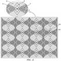
도 2는 본 발명의 정전용량방식 터치패널의 전극의 메쉬 패턴을 모식적으로 도시한 것이다.
도 3은 본 발명의 제1 전극 및 제2 전극이 교차형성되는 부분의 일 예이다.
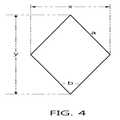
도 4는 본 발명의 유닛메쉬의 일 예로 유닛메쉬의 한변의 길이는 a, 내각은 b, 폭은 x 및 길이는 y인 것을 나타낸다.
도 5는 본 발명의 유닛메쉬를 포함하는 하나의 유닛셀을 도식화하여 나타낸 것이다.
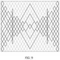
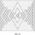
도 6 내지 도 11은 본 발명의 전극의 금속메쉬 패턴의 일예를 도시한 것이다.
도 12는 본 발명의 실시예 1의 금속메쉬로 이루어진 제1 전극 및 제2 전극이 연결부메쉬에 의해 교차형성된 일 예이다.
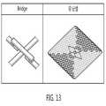
도 13은 본 발명의 실시예 3의 금속메쉬로 이루어진 제1 전극 및 제2 전극이 연결부메쉬에 의해 교차형성되고 메쉬브릿지를 추가로 포함하는 경우의 일 예이다.
도 14는 본 발명의 일 예로 터치패널을 형성하는 단계를 설명한 도이다.1 is an example of a conventional single-layer electrode pattern.
2 schematically shows a mesh pattern of electrodes of the capacitive touch panel of the present invention.
3 is an example of a portion where the first electrode and the second electrode of the present invention are cross-formed.
FIG. 4 shows an example of the unit mesh of the present invention, wherein a length of one side of the unit mesh is a, an interior angle is b, a width is x, and a length is y.
5 is a schematic representation of one unit cell comprising a unit mesh of the present invention.
Figs. 6 to 11 illustrate an example of a metal mesh pattern of the electrode of the present invention.
12 is an example in which the first electrode and the second electrode made of the metal mesh according to the first embodiment of the present invention are crossed by the connection mesh.
13 is an example of a case where the first electrode and the second electrode made of the metal mesh according to the third embodiment of the present invention are cross-formed by a connecting portion mesh and further include a mesh bridge.
FIG. 14 is a diagram illustrating a step of forming a touch panel as an example of the present invention.
본 발명은 본 발명은 하나의 기판 상에 서로 다른 방향으로 교차형성되는 제1 전극과 제2 전극을 포함하고,The present invention provides a plasma display panel comprising a first electrode and a second electrode cross-formed on one substrate in different directions,
상기 제1 전극은 각각 복수개의 마름모꼴 유닛메쉬로 이루어진 복수개의 마름모꼴의 유닛셀이 연결부메쉬를 통하여 연결되어 형성되고, 상기 제2 전극은 각각 복수개의 마름모꼴 유닛메쉬로 이루어진 복수개의 마름모꼴의 유닛셀이 제1 전극과의 교차부에서 서로 분리되어 메쉬브릿지에 의해 연결되어 형성되는 것을 특징으로 하는 정전용량방식 터치패널에 관한 것이다.Wherein the first electrode is formed by connecting a plurality of diamond-shaped unit cells each having a plurality of diamond-like unit meshes through a connection mesh, and the second electrode comprises a plurality of diamond-shaped unit cells each having a plurality of diamond- And the electrodes are separated from each other at intersections with the first electrodes and connected to each other by the mesh bridges.
본 발명의 정전용량방식 터치패널에서, 상기 제1 전극은 구동전극이 될 수 있으며, 그 경우 상기 제2 전극은 감지전극이 된다. 동일하게 상기 제1 전극은 감지전극이 될 수 있으며, 그 경우 상기 제2 전극은 구동전극이 된다.
In the capacitive touch panel of the present invention, the first electrode may be a driving electrode, and the second electrode may be a sensing electrode. Similarly, the first electrode may be a sensing electrode, and the second electrode may be a driving electrode.
즉, 본 발명은 상호정전용량방식 터치패널로써, 구동전극에 전압이 인가됨에 따라 감지전극과 구동전극 사이에서 발생하는 캐패시턴스의 변화를 통해 사용자의 터치 지점을 측정하는 방식의 터치패널이다.
That is, the present invention is a touch panel of a mutual capacitance type touch panel in which a touch point of a user is measured through a change in capacitance occurring between a sensing electrode and a driving electrode as a voltage is applied to the driving electrode.
이하, 상기 제1 전극이 구동전극이고 제2 전극이 감지전극인 경우를 예로들어 본 발명을 설명하고자 하나, 그 반대의 경우인 제1 전극이 감지전극이고 제2 전극이 구동전극인 경우도 본 발명의 범위에서 배제되는 것은 아니다.
Hereinafter, the present invention will be described by taking the case where the first electrode is a driving electrode and the second electrode is a sensing electrode. In the opposite case, the first electrode is a sensing electrode and the second electrode is a driving electrode. It is not excluded from the scope of the invention.
이하에서, 첨부된 도면을 참고하여 본 발명의 실시예에 대하여 상세히 설명한다. 본 발명을 설명하기에 앞서 관련된 공지기능 및 구성에 대한 구체적 설명이 본 발명의 요지를 불필요하게 흐릴 수 있다고 판단되는 경우 그에 대한 설명은 생략하기로 한다.Hereinafter, embodiments of the present invention will be described in detail with reference to the accompanying drawings. In the following description, well-known functions or constructions are not described in detail since they would unnecessarily obscure the gist of the present invention.
아래 설명과 도면은 당업자가 설명되는 장치와 방법을 용이하게 실시할 수 있도록 특정 실시예를 예시한다. 다른 실시예는 구조적, 논리적으로 다른 변형을 포함할 수 있다. 개별 구성 요소와 기능은 명확히 요구되지 않는 한, 일반적으로 선택될 수 있으며, 과정의 순서는 변할 수 있다. 몇몇 실시예의 부분과 특징은 다른 실시예에 포함되거나 다른 실시예로 대체될 수 있다.
The following description and drawings illustrate specific embodiments in order that those skilled in the art can readily implement the described apparatus and method. Other embodiments may include other variations, both structurally and logically. Unless explicitly required, individual components and functions may be selected generally, and the order of the processes may vary. Portions and features of some embodiments may be included in other embodiments or may be replaced by other embodiments.
도 2 및 3에 도시된 바와 같이, 구동전극(1)은 복수개의 마름모꼴 유닛메쉬(10)로 이루어진 복수개의 마름모꼴의 유닛셀(20)이 연결부메쉬(2)를 통하여 연결되어 있다.As shown in FIGS. 2 and 3, the
상기 구동전극(1)은 감지전극(3)이 형성된 면과 동일면상에 메쉬구조로 형성되어 감지전극과 교차하도록 위치한다. 구동전극(1)은 배선을 통해 전압원과 연결되어 구동전극에 전압이 인가되는 경우, 구동전극과 감지전극 사이에 전기장이 발생하게 된다.The
상기 구동전극(1) 또는 감지전극(3)에 포함되는 유닛셀(20) 내에 포함되는 유닛메쉬(10)들은 동일한 형태로 형성될 수 있으며, 인접하는 다른 유닛메쉬(10)들과 하나의 모서리 부분이 서로 대칭되게 맞닿아 있거나 하나의 변을 공통으로 하는 형태로 형성되어 서로 전류가 통할 수 있다.The
감지전극(3)은 사용자의 접촉을 감지하는 부분으로 투명기판의 일면에 메쉬구조로 형성된다. 감지전극(3)은 복수개의 마름모꼴 유닛메쉬로 이루어진 복수개의 마름모꼴의 유닛셀이 구동전극(1)과의 교차부에서 서로 분리되어 메쉬브릿지(5)에 의해 연결된다. 메쉬브릿지의 일 실시형태는 도 9 및 도 10에 도시되어 있다.The
본 발명의 구동전극과 감지전극은 패터닝된 선으로 이루어진 메쉬구조로 되어 있고, 이 때 패터닝된 선의 두께 및 폭을 수 ㎛로 미세하게 하면 개구율(패터닝된 선의 면적을 제외한 면적에 대한 전체 면적의 비율)이 95% 내지 99.5%에 이를 수 있는 장점이 있다. 이와 같이 메쉬구조의 개구율을 증가시킴으로써, 터치패널의 투과율(입사광에 대한 투과광에 대한 비율)을 높일 수 있고 시인성을 향상시킬 수 있다.The driving electrode and the sensing electrode of the present invention have a mesh structure formed by patterned lines. When the thickness and width of the patterned line are reduced to several micrometers, the aperture ratio (the ratio of the total area to the area excluding the area of the patterned line ) To 95% to 99.5%. By increasing the aperture ratio of the mesh structure in this manner, the transmittance of the touch panel (the ratio of the incident light to the transmitted light) can be increased and the visibility can be improved.
또한 본 발명의 구동전극과 감지전극은 메쉬구조로 되어 있어서 면적(패터닝된 선의 면적)이 작고, 면저항값이 작아서 터치패널의 터치 감지속도가 빠르며 따라서 전력 소모가 적다.In addition, since the driving electrode and the sensing electrode of the present invention have a mesh structure, the area (area of the patterned line) is small and the sheet resistance value is small, so that the touch sensing speed of the touch panel is fast and the power consumption is low.
바람직하게는 상기 메쉬의 폭은 1~10㎛, 보다 바람직하게는 1~5㎛이다.
Preferably, the width of the mesh is 1 to 10 탆, more preferably 1 to 5 탆.
도 2 및 도 3에 도시된 바와 같이, 본 발명의 터치패널에서 상기 감지전극(3)의 메쉬브릿지(5)는 인접하는 구동전극(1)의 유닛셀(20)을 통과하여 형성될 수 있으며, 하나 이상이 형성될 수 있다.2 and 3, in the touch panel of the present invention, the
또한, 본 발명의 터치패널은 구동전극(1)의 유닛셀(20) 사이를 연결하는 하나 이상의 메쉬브릿지(4)를 더 포함할 수 있으며, 상기 메쉬브릿지는 인접하는 감지 전극의 유닛셀을 통과하여 형성될 수 있다.
The touch panel of the present invention may further include one or
상기와 같이 메쉬브릿지를 추가하는 경우 단일층에 감지전극과 구동전극의 형성으로 인한 전극간 접촉영역의 감소 및 이에 따른 상호정전용량의 감소를 해소할 수 있다. 즉, 본 발명은 감지전극 및 구동전극을 메쉬구조로 형성하고 상기 메쉬구조의 감지전극 유닛셀 및 메쉬구조의 구동전극 유닛셀을 각각 구동전극 메쉬브릿지 및 감지전극 메쉬브릿지가 통과하게 함으로써, 저항은 낮추면서, 감지전극과 구동전극간의 접촉면적을 늘려주어 상호정전용량을 높여줄 수 있다. 이로 인해 외부 노이즈의 영향을 적게 받는 효과가 있다. 또한 RC 타임을 감소시켜 구동능력을 향상시켜줄 수 있다.
When the mesh bridge is added as described above, it is possible to reduce the contact area between the electrodes due to the formation of the sensing electrode and the driving electrode in the single layer, and thus the reduction of the mutual capacitance. That is, according to the present invention, the sensing electrode and the driving electrode are formed in a mesh structure, and the driving electrode unit cell of the mesh structure and the driving electrode unit cell of the mesh structure are respectively passed through the driving electrode mesh bridge and the sensing electrode mesh bridge, The contact area between the sensing electrode and the driving electrode can be increased and the mutual capacitance can be increased. This has the effect of less influencing the external noise. In addition, the RC time can be reduced to improve the driving capability.
본 발명의 일실시예에서 감지전극의 유닛메쉬, 구동전극의 유닛메쉬, 및/또는 감지전극의 연결부메쉬는, 도 4에 도시된 바와 같이, 한변의 길이가 a이고 내각이 b인 마름모꼴(폭 x, 길이 y)일 수 있다. 본 발명에서 하나의 유닛셀(폭 X, 길이 Y. 도 5 참조)은 유닛메쉬들을 수직방향 및 수평방향의 대칭형태로 배치한 것일 수 있다. 따라서 유닛메쉬의 크기 및 유닛셀의 크기는4, the unit mesh of the sensing electrode, the unit mesh of the driving electrode, and / or the connecting portion mesh of the sensing electrode in the embodiment of the present invention are formed of a rhombus (width x, length y). In the present invention, one unit cell (width X, length Y, see Fig. 5) may be arranged in a symmetrical arrangement of the unit meshes in the vertical direction and the horizontal direction. Therefore, the size of the unit mesh and the size of the unit cell are
X = nxX = nx
Y = nyY = ny

이때 n은 유닛셀을 이루고 있는 유닛메쉬의 수이다.Where n is the number of unit meshes that make up the unit cell.
유닛메쉬에서 x : y = 1 : 1 ~ 1 : 2 일 수 있다.In the unit mesh, x: y = 1: 1 to 1: 2.
내각 b는 바람직하게는 45도 내지 135도이다.
The cabinet b is preferably 45 degrees to 135 degrees.
감지전극과 구동전극의 교차 각도는 유닛메쉬의 각도인 b의 범위일 수 있다.
The intersection angle of the sensing electrode and the driving electrode may be in the range of b, which is the angle of the unit mesh.
상기 구동전극의 메쉬브릿지(4) 및 감지전극의 메쉬브릿지(5)는 각각 1개 또는 2개 이상일 수 있다. 또한, 최단 경로(P)로 구성되는 것이 바람직하다. 최단경로 P는 메쉬브릿지의 시작점과 끝점의 거리에 의해 결정된다.The mesh bridges 4 of the driving electrodes and the mesh bridges 5 of the sensing electrodes may be one or more than two. Further, it is preferable that it is constituted by the shortest path (P). The shortest path P is determined by the distance between the start point and the end point of the mesh bridge.
도 6의 경우 구동전극간 거리는 3x이다. 때문에 위 경우의 구동전극 메쉬브릿지의 최단 거리 Px=3x(6a)가 된다. 감지전극간 메쉬브릿지의 시작점과 끝점은 2y 거리를 가지므로, 감지전극 메쉬브릿지의 최단 거리 Py=2y(4a)가 된다.6, the distance between the driving electrodes is 3x. Therefore, the shortest distance Px of the driving electrode mesh bridge in the above case becomes Px = 3x (6a). Since the start and end points of the mesh bridge between the sensing electrodes have a distance of 2y, the shortest distance Py of the sensing electrode mesh bridge is Py = 2y (4a).
도 7의 경우에도 최단거리 P는 구동전극 및 감지전극의 메쉬브릿지의 시작점과 끝점의 거리에 따라 일정하게 형성되는 것을 볼 수 있다.7, the shortest distance P is formed to be constant depending on the distance between the start point and the end point of the mesh bridge of the driving electrode and the sensing electrode.
Px = 3x = 6aPx = 3x = 6a
Py = 4y = 8a
Py = 4y = 8a
도 6 내지 도 11에서 점선은 더미패턴을 의미한다.
6 to 11, the dotted line means a dummy pattern.
본 발명의 또 다른 일예인 도 8의 경우, 최단경로는 다음과 같다.In the case of Fig. 8 which is another example of the present invention, the shortest path is as follows.
Px= 7x = 14aPx = 7x = 14a
Py= 7y = 14a
Py = 7y = 14 a
도 9의 경우 감지전극의 메쉬브릿지 시작점과 끝점이 같다면, 메쉬브릿지의 형태는 다양하게 성립될 수 있는 것을 보여준다.9, the shape of the mesh bridge can be variously formed if the start and end points of the mesh bridge of the sensing electrode are the same.
결론적으로 메쉬브릿지의 거리는 구동전극과 감지전극이 도통될 수 있는 최소값인 2a이상의 값을 갖는다. 따라서 구동전극의 메쉬브릿지의 최단경로 Px는 2a ≤ Px ≤ mx×2a-4a 값으로 결정될 수 있다.(mx는 구동전극 유닛셀(Unit cell) 내의 유닛메쉬의 최대갯수) 감지전극의 메쉬브릿지 최단경로 Py는 2a ≤ Py ≤ my×2a-4a 값으로 결정될 수 있다.(my는 감지전극 유닛셀(Unit cell) 내의 유닛메쉬의 최대갯수) 이때 최단경로 Px 및 Py는 대칭형으로 구성되는 것이 바람직하다.As a result, the distance of the mesh bridge has a value equal to or larger than 2a, which is the minimum value at which the driving electrode and the sensing electrode can be conducted. Therefore, the shortest route Px of the mesh bridge of drive electrodes may be determined in2a ≤ P x ≤ m x × 2a-4a value. (Mx the maximum number of unit mesh in a driving electrode unit cells (Unit cell)) sensing electrodes of a mesh bridge shortest path Py may be determined by2a ≤ P y ≤ m y × 2a-4a value. (my is the sensing electrode unit cells (the maximum number of unit mesh in the unit cell)) the shortest path Px and Py is preferably symmetrical.
도 10 및 11은 구동전극 메쉬브릿지(도 10) 및 감지전극 메쉬브릿지(도 11)의 최단 거리 및 최대 거리를 나타낸다.
10 and 11 show the shortest distance and the maximum distance of the driving electrode mesh bridge (FIG. 10) and the sensing electrode mesh bridge (FIG. 11).
또한 최단 경로 확보를 위해 구동전극 내부로 감지전극의 메쉬브릿지가 통과하는 경우 구동전극을 브릿지로 연결하고, 감지전극 내부로 구동전극 메쉬브릿지가 교차하는 경우 감지전극을 브릿지로 연결하는 것이 바람직하다.In order to secure the shortest path, it is preferable that the driving electrode is connected to the bridge when the mesh bridge of the sensing electrode passes through the driving electrode and the sensing electrode is connected to the sensing electrode when the driving electrode mesh bridge intersects the sensing electrode.
RC의 균일성 확보를 위해, 상기 감지전극과 구동전극은 대칭형태로 구현되는 것이 바람직하다.
In order to ensure the uniformity of the RC, it is preferable that the sensing electrode and the driving electrode are realized in a symmetrical form.
본 발명의 상기 감지전극 및 상기 구동전극은 금속막으로 형성될 수 있다. 상기 금속막은 구리(Cu), 알루미늄(Al), 금(Au), 은(Ag), 니켈(Ni), 크롬(Cr) 또는 이들 금속의 합금으로 형성될 수 있으며, 더욱 바람직하게는 전기전도도가 높은 구리(Cu), 알루미늄(Al), 금(Au), 은(Ag) 또는 이들 금속의 합금으로 형성될 수 있다. 또한, 상기 감지전극 및 상기 구동전극은 전도성 산화막으로 형성될 수도 있다. 상기 전도성 산화막은 ITO, FTO, AZO, IZO, GZO, ATO, NTO 중 선택된 적어도 하나의 산화물로 형성될 수 있다.The sensing electrode and the driving electrode of the present invention may be formed of a metal film. The metal film may be formed of copper (Cu), aluminum (Al), gold (Au), silver (Ag), nickel (Ni), chromium (Cr), or an alloy of these metals, And may be formed of high copper (Cu), aluminum (Al), gold (Au), silver (Ag), or an alloy of these metals. Also, the sensing electrode and the driving electrode may be formed of a conductive oxide film. The conductive oxide film may be formed of at least one oxide selected from ITO, FTO, AZO, IZO, GZO, ATO and NTO.
또한, 상기 감지전극 및 상기 구동전극은 금속 단막이거나 금속막과 전도성 산화막이 적층된 형태, 예컨대 전도성 산화막 위에 금속막이 적층된 형태일 수 있다.The sensing electrode and the driving electrode may be a metal thin film or a stacked structure of a metal film and a conductive oxide film, for example, a metal film stacked on a conductive oxide film.
상기 메쉬구조의 감지전극 및 구동전극은 투명기판에 도금(Plating), 스퍼터링(Sputtering), 증착(Evaporation) 등을 통해 형성하거나, 실크스크린법, 그라비아 인쇄법(Gravure Printing) 또는 잉크젯 인쇄법(Inkjet Printing)의 인쇄공정을 이용하여 형성될 수 있다.The sensing electrode and the driving electrode of the mesh structure may be formed on a transparent substrate by plating, sputtering, evaporation, or the like, or may be formed by a silk screen method, a gravure printing method or an inkjet printing method Printing may be used.
본발명의 감지전극 및 구동전극이 교차하는 부분의 브릿지는 감지전극 및 구동전극을 형성하는 방법과 동일한 통상의 방법을 제한없이 사용하여 형성할 수 있다.The bridge at the intersection of the sensing electrode and the driving electrode of the present invention can be formed by using the same conventional method as the method of forming the sensing electrode and the driving electrode without limitation.
상기 감지전극 및 구동전극은 메쉬브릿지와 유기절연막 또는 무기절연막으로 절연될 수 있으며, 접촉부분에 패턴을 형성하지 않는 방법으로 절열시킬 수도 있다(도 3 참고).The sensing electrode and the driving electrode may be insulated by a mesh bridge, an organic insulating film, or an inorganic insulating film, or may be thermally insulated by a method of not forming a pattern at a contact portion (see FIG. 3).
상기 유기 절연막은 실리콘계 유기절연막 또는 Hybrid Type 유기절연막일 수 있고 상기 무기절연막은 실리콘 산화물(Silicon Oxide)계 무기절연막일 수 있다.
The organic insulating layer may be a silicon-based organic insulating layer or a hybrid-type organic insulating layer, and the inorganic insulating layer may be a silicon oxide-based inorganic insulating layer.
본 발명에서 상기 메쉬브릿지는 구동전극 및 감지전극과의 오버레이가 1.5㎛ 이하로 작게 형성될 수 있다.
In the present invention, the mesh bridge may be formed such that the overlay with the driving electrode and the sensing electrode is as small as 1.5 m or less.
일반적으로 금속으로 감지전극 및 구동전극을 형성할 때 금속의 불투명한 색상으로 인해 터치패널의 투과율이 떨어지는 문제점이 있으나, 본 발명은 메쉬구조로 선폭 및 두께를 수 ㎛로 미세하게 패터닝하여 개구율을 증가시킴으로써, 터치패널의 투과율을 향상시킬 수 있다. 본 발명은 이와 같이 전기전도도가 높은 금속으로 감지전극 및 구동전극을 형성하여 바람직하게는 면저항 150Ω/□ 이하의 높은 전기전도도를 가지며, 또한 메쉬구조로 형성함으로써 터치패널의 투과율이 89% 이상으로 우수한 시인성을 갖는다.In general, when the sensing electrode and the driving electrode are formed of metal, there is a problem that the transmittance of the touch panel is lowered due to the opaque color of the metal. However, the present invention uses a mesh structure to finely pattern the line width and thickness to several 탆, The transmittance of the touch panel can be improved. In the present invention, the sensing electrode and the driving electrode are formed of a metal having a high electrical conductivity as described above, and preferably have a high electrical conductivity of not more than 150 Ω / □ and have a mesh structure. Thus, the touch panel has a transmittance of 89% It has visibility.
본 발명에 따른 터치패널은 종래의 두개의 투명기판에 각각 형성된 감지전극과 구동전극을 단일층에 형성함으로써 터치패널의 박형화를 이룰 수 있다. 또한, 디스플레이에서 제공하는 영상이 통과하는 터치패널의 두께가 줄어들어 터치패널의 시인성이 향상된다.
The touch panel according to the present invention can reduce the size of the touch panel by forming the sensing electrode and the driving electrode formed on the two transparent substrates in a single layer. In addition, the thickness of the touch panel through which the image provided by the display passes is reduced, thereby improving the visibility of the touch panel.
이하 본 발명의 터치패널을 형성하는 방법의 일례를 도 14를 예로 설명한다.Hereinafter, an example of a method of forming the touch panel of the present invention will be described with reference to FIG. 14 as an example.
본 발명의 터치패널은The touch panel of the present invention
투명기판 상에 1차 산화막 및 메탈막을 형성하는 1 단계,A first step of forming a first oxide film and a metal film on a transparent substrate,
1차 메탈막상에 감광물질(photo resist(PR))을 도포한 후, 감광물질을 메쉬 패턴이 형성된 포토마스크를 사용하여 노광 시키는 2 단계,A photoresist (PR) is applied on the primary metal film, and then the photosensitive material is exposed using a photomask having a mesh pattern.
상기 감광물질을 현상(develop) 시킨 후 1차 메탈막 및 산화막을 습식 식각 용액 또는 건식 식각 방법을 사용하여 식각하여 1차 산화막 및 메탈 패턴을 형성하는 3 단계Developing the photosensitive material and then etching the first metal film and the oxide film using a wet etching solution or a dry etching method to form a first oxide film and a metal pattern
상기 1차 메탈 패턴상에 무기 또는 유기 절연막을 형성하는 4 단계,A fourth step of forming an inorganic or organic insulating film on the primary metal pattern,
상기 절연막상에 감광물질(PR)을 도포한 후, 감광물질을 Hole 패턴이 형성된 포토마스크를 사용하여 노광 시키는 5 단계,Applying a photosensitive material (PR) on the insulating film, and then exposing the photosensitive material using a photomask having a hole pattern,
상기 절연막상을 습식 식각 용액 또는 건식 식각 방법을 사용하여 식각하여 연결부 Hole을 형성하는 6 단계,Etching the insulating film on the insulating film using a wet etching solution or a dry etching method to form a connection hole,
상기 절연막상에 2차 산화막 및 메탈막을 형성하는 7 단계,A seventh step of forming a secondary oxide film and a metal film on the insulating film,
2차 메탈막상 감광물질(photo resist(PR))을 도포한 후 감광물질상 메쉬브릿지 패턴이 형성된 포토마스크를 사용하여 노광 시키는 8 단계,8 steps of applying a secondary metal film photosensitive material (photo resist (PR)) and then exposing it using a photomask having a mesh bridge pattern on the photosensitive material,
상기 감광물질을 현상(develop) 시킨 후 2차 메탈막 및 산화막을 습식 식각 용액 또는 건식 식각 방법을 사용하여 식각하여 2차 산화막 및 메쉬브릿지 패턴을 형성하는 9 단계,Developing the photosensitive material, and then etching the second metal film and the oxide film using a wet etching solution or a dry etching method to form a second oxide film and a mesh bridge pattern,
상기 2차 메쉬브릿지 패턴상에 무기 또는 유기 절연막을 형성하는 10 단계를 통하여 제조될 수 있다.
And forming an inorganic or organic insulating film on the secondary mesh bridge pattern.
이하 구체적인 실시예에 의해 본 발명을 설명하나, 본 발명이 이들 실시예에 한정되지 않으며, 본 발명의 기술적 사상 내에서 당해 분야의 통상의 지식을 가진 자에 의해 그 변형이나 개량이 가능함은 명백하다고 할 것이다. 본 발명의 단순한 변형 내지 변경은 모두 본 발명의 영역에 속하는 것으로 본 발명의 구체적인 보호 범위는 첨부된 특허청구범위에 의해서 명확해질 것이다.
The present invention will now be described with reference to specific examples, but it should be apparent that the present invention is not limited to these examples and that variations and modifications can be made by those skilled in the art within the technical scope of the present invention something to do. It will be understood by those skilled in the art that various changes in form and details may be made therein without departing from the spirit and scope of the invention as defined by the appended claims.
실시예Example 1 One
하기 방법에 의해 유닛셀 내의 유닛메쉬의 수 mx=20, my=10이고, 구동전극의 유닛셀은 연결부메쉬로 연결되고, 감지전극의 유닛셀은 하나의 메쉬브릿지로 연결된 형태의 패턴을 갖는 기판(도 8 참조)을 제조하였다.The number of unit meshes mx = 20, my = 10 in the unit cell, the unit cells of the driving electrode are connected by a connecting mesh, and the unit cells of the sensing electrode are connected by a single mesh bridge. (See Fig. 8).
투명기판 상에 1차 산화막(ITO, IZO) 및 메탈막(Mo 및 Ag 합금)을 형성하는 1 단계,A first step of forming a primary oxide film (ITO, IZO) and a metal film (Mo and Ag alloy) on a transparent substrate,
1차 메탈막상에 감광물질(photo resist(PR))을 도포한 후 감광물질을 메쉬 패턴이 형성된 포토마스크를 사용하여 노광 시키는 2 단계,A photoresist (PR) is applied on a primary metal film, and then a photosensitive material is exposed using a photomask having a mesh pattern.
상기 감광물질을 현상(develop) 시킨 후 1차 메탈막 및 산화막을 습식 식각용액을 사용하여 1차 산화막 및 메탈 패턴을 형성하는 3 단계,Developing the photosensitive material, forming a primary oxide film and a metal pattern using a wet etching solution on the primary metal film and the oxide film,
상기 1차 메탈 패턴상에 무기 절연막(SiO2)을 형성하는 4 단계,A fourth step of forming an inorganic insulating film (SiO2) on the primary metal pattern,
상기 절연막상에 감광물질(PR)을 도포한 후 감광물질을 Hole 패턴이 형성된 포토마스크를 사용하여 노광 시키는 5 단계,Applying a photosensitive material (PR) on the insulating film, and exposing the photosensitive material to light using a photomask having a hole pattern,
상기 절연막상에 건식 식각 방법을 사용하여 연결부 Hole을 형성하는 6 단계,A sixth step of forming a connection portion Hole on the insulating film using a dry etching method,
상기 절연막상에 2차 산화막 및 메탈막을 형성하는 7 단계,A seventh step of forming a secondary oxide film and a metal film on the insulating film,
2차 메탈막상에 감광물질(photo resist(PR))을 도포한 후 감광물질을 메쉬브릿지 패턴이 형성된 포토마스크를 사용하여 노광 시키는 8 단계After the photosensitive material (PR) is applied on the secondary metal film, the photosensitive material is exposed using a photomask having a mesh bridge pattern.
상기 감광물질을 현상(develop) 시킨 후 2차 메탈막 및 산화막을 습식 식각 용액을 사용하여 2차 산화막 및 메쉬브릿지 패턴을 형성하는 9 단계,Developing the photosensitive material, and then forming a secondary oxide film and a mesh bridge pattern using a wet etching solution on the secondary metal film and the oxide film,
상기 2차 메쉬브릿지 패턴상에 무기 또는 유기 절연막을 형성하는 10 단계를 통하여 감지전극 및 구동전극이 형성된 기판을 제조하였다.
The substrate on which the sensing electrode and the driving electrode were formed was fabricated through ten steps of forming an inorganic or organic insulating film on the secondary mesh bridge pattern.
실시예Example 2 ~ 5 2 to 5
실시예 1의 방법과 동일한 방법으로 구동전극 및 감지전극이 다수개의 메쉬브릿지로 연결된 기판을 제조하였다.
A substrate having a driving electrode and a sensing electrode connected to each other by a plurality of mesh bridges was fabricated in the same manner as in Example 1.
실험예Experimental Example
상기 실시예 1 ~5에서 만든 기판에 대해 메쉬브릿지 경로에 따른 기판의 저항 및 상호정전용량을 측정하고 하기 표 1 에 나타내었다. 이때 유닛셀에서 메쉬브릿지 경로가 추가될 경우 유닛셀 저항은 감소하고, 상호정전용량은 증가하는 것을 알 수 있다. 한편, 실시예 4 및 5의 경우 메쉬브릿지 경로가 추가되어 저항이 감소되었음에도 불구하고, 상호정전용량의 증가로 RC Time은 오히려 실시예 3보다 증가된 것을 알 수 있다.Resistance and mutual capacitance of the substrate according to the mesh bridge path were measured for the substrates prepared in Examples 1 to 5, and the results are shown in Table 1 below. At this time, when the mesh bridge path is added in the unit cell, the unit cell resistance decreases and the mutual capacitance increases. On the other hand, in the case of Examples 4 and 5, although the resistance of the mesh bridge path was added and the resistance was decreased, it was found that the RC time was increased rather than that of Example 3 due to the mutual capacitance increase.
(Px /(Px /PyPy))
Claims (14)
Translated fromKorean상기 제1 전극은 각각 복수개의 마름모꼴 유닛메쉬로 이루어진 복수개의 마름모꼴의 유닛셀이 연결부메쉬를 통하여 연결되어 형성되고, 상기 제2 전극은 각각 복수개의 마름모꼴 유닛메쉬로 이루어진 복수개의 마름모꼴의 유닛셀이 제1 전극과의 교차부에서 서로 분리되어 메쉬브릿지에 의해 연결되어 형성되는 것을 특징으로 하는 정전용량방식 터치패널.A first electrode and a second electrode formed on one substrate in cross directions in different directions,
Wherein the first electrode is formed by connecting a plurality of diamond-shaped unit cells each having a plurality of diamond-like unit meshes through a connection mesh, and the second electrode comprises a plurality of diamond-shaped unit cells each having a plurality of diamond- Wherein the first electrode and the second electrode are separated from each other at an intersection with the first electrode and connected to each other by a mesh bridge.
상기 제2 전극의 메쉬브릿지는 인접하는 제1 전극 유닛셀을 통과하여 형성되며, 하나 이상이 포함되는 것을 특징으로 하는 정전용량방식 터치패널.The method according to claim 1,
Wherein the mesh bridge of the second electrode is formed to pass through the adjacent first electrode unit cell, and at least one of the mesh bridges is included.
제1 전극의 유닛셀 사이를 연결하는 하나 이상의 메쉬브릿지를 더 포함하며, 상기 메쉬브릿지는 인접하는 제2 전극의 유닛셀을 통과하여 형성되는 것을 특징으로 하는 정전용량방식 터치패널.The method of claim 2,
The touch panel of claim 1, further comprising one or more mesh bridges connecting unit cells of the first electrode, wherein the mesh bridges are formed through unit cells of adjacent second electrodes.
유닛메쉬의 한변의 길이를 a라고 하고 내각을 b라고 할 때 내각 b는 45 내지 135도 인 것을 특징으로 하는 정전용량방식 터치패널.The method according to claim 1,
And the internal angle b is 45 to 135 degrees when the length of one side of the unit mesh is a and the internal angle is b.
유닛메쉬의 폭을 x, 길이를 y라고 할 때, 제1전극의 메쉬브릿지의 최단경로 Px는 2a ≤ Px ≤ mx×2a-4a이고, 제2전극의 메쉬브릿지 최단경로 Py는 2a ≤ Py ≤ my×2a-4a이며, mx 및 my는 각각 유닛셀 내의 유닛메쉬의 최대갯수인 것을 특징으로 하는 정전용량방식 터치패널.The method of claim 4,
The shortest path Px of the mesh bridge of the first electrode is 2a? Px ? Mx ? 2a-4a, and the shortest path Py of the mesh bridge of the second electrode is Py2a ≤ P y ≤ m y × 2a-4a is, mx and my are the capacitance type touch panel which is characterized in that the maximum number of units, each unit cell in the mesh.
상기 제1 전극 및 제2 전극은 금속막으로 형성되는 것을 특징으로 하는 정전용량방식 터치패널.The method according to claim 1,
Wherein the first electrode and the second electrode are formed of a metal film.
상기 금속막은 구리(Cu), 알루미늄(Al), 금(Au), 은(Ag), 니켈(Ni), 크롬(Cr) 또는 이들 금속의 합금으로 형성되는 것을 특징으로 하는 정전용량방식 터치패널.The method of claim 6,
Wherein the metal film is formed of copper (Cu), aluminum (Al), gold (Au), silver (Ag), nickel (Ni), chrome (Cr), or an alloy of these metals.
상기 제1 전극 및 제2 전극은 전도성 산화막으로 형성되는 것을 특징으로 하는 정전용량방식 터치패널.The method according to claim 1,
Wherein the first electrode and the second electrode are formed of a conductive oxide film.
상기 제1 전극 및 제2 전극은 전도성 산화막 위에 금속막이 적층된 형태로 형성되는 것을 특징으로 하는 정전용량방식 터치패널.The method according to claim 1,
Wherein the first electrode and the second electrode are formed of a metal film stacked on the conductive oxide film.
상기 제1 전극 및 제2 전극은 메쉬브릿지와 실리콘계 유기절연막 또는 하이브리드형 유기절연막으로 절연되는 것을 특징으로 하는 정전용량방식 터치패널.The method according to claim 1,
Wherein the first electrode and the second electrode are insulated by a mesh bridge and a silicon-based organic insulation layer or a hybrid-type organic insulation layer.
상기 제1 전극 및 제2 전극은 메쉬브릿지와 실리콘산화물(Silicon Oxide)계 무기절연막으로 절연되는 것을 특징으로 하는 정전용량방식 터치패널.The method according to claim 1,
Wherein the first electrode and the second electrode are insulated by a mesh bridge and a silicon oxide inorganic insulating film.
상기 제1 전극이 구동전극이고 상기 제2 전극이 감지전극이거나, 상기 제1 전극이 감지전극이고 상기 제2 전극이 구동전극인 것을 특징으로 하는 정전용량방식 터치패널.The method according to claim 1,
Wherein the first electrode is a driving electrode, the second electrode is a sensing electrode, the first electrode is a sensing electrode, and the second electrode is a driving electrode.
상기 메쉬브릿지는 제1 전극 및 제 2전극과의 오버레이가 1.5㎛ 이하인 것을 특징으로 하는 정전용량방식 터치패널.The method according to claim 1,
Wherein the mesh bridge has an overlay with the first electrode and the second electrode of 1.5 占 퐉 or less.
Priority Applications (2)
| Application Number | Priority Date | Filing Date | Title |
|---|---|---|---|
| PCT/KR2015/004235WO2015167212A1 (en) | 2014-04-29 | 2015-04-28 | Capacitive-type touchpanel |
| TW104113677ATWI663538B (en) | 2014-04-29 | 2015-04-29 | Capacitive touch panel and display device comprising the same |
Applications Claiming Priority (2)
| Application Number | Priority Date | Filing Date | Title |
|---|---|---|---|
| KR20140051230 | 2014-04-29 | ||
| KR1020140051230 | 2014-04-29 |
Publications (2)
| Publication Number | Publication Date |
|---|---|
| KR20150124907Atrue KR20150124907A (en) | 2015-11-06 |
| KR102336971B1 KR102336971B1 (en) | 2021-12-09 |
Family
ID=54601163
Family Applications (1)
| Application Number | Title | Priority Date | Filing Date |
|---|---|---|---|
| KR1020150059456AActiveKR102336971B1 (en) | 2014-04-29 | 2015-04-28 | Capacitive Type Touch Panel |
Country Status (2)
| Country | Link |
|---|---|
| KR (1) | KR102336971B1 (en) |
| TW (1) | TWI663538B (en) |
Cited By (2)
| Publication number | Priority date | Publication date | Assignee | Title |
|---|---|---|---|---|
| EP3276470A1 (en)* | 2016-07-29 | 2018-01-31 | Samsung Display Co., Ltd. | Display apparatus |
| US11868573B2 (en) | 2021-02-15 | 2024-01-09 | Samsung Display Co., Ltd. | Electronic apparatus |
Families Citing this family (4)
| Publication number | Priority date | Publication date | Assignee | Title |
|---|---|---|---|---|
| TWI581152B (en)* | 2016-01-20 | 2017-05-01 | Intelligent touch touch device | |
| CN112578934B (en)* | 2020-12-07 | 2022-11-29 | 昆山国显光电有限公司 | Touch panel and display panel |
| TWI783743B (en)* | 2021-10-21 | 2022-11-11 | 友達光電股份有限公司 | Touch device |
| WO2023092348A1 (en) | 2021-11-24 | 2023-06-01 | 京东方科技集团股份有限公司 | Touch control layer and touch control display apparatus |
Citations (4)
| Publication number | Priority date | Publication date | Assignee | Title |
|---|---|---|---|---|
| KR101322333B1 (en)* | 2012-07-30 | 2013-10-28 | 이엘케이 주식회사 | Touch screen panel of metal mesh and method of fabricating the same |
| KR20130141761A (en) | 2012-06-18 | 2013-12-27 | (주)티메이 | Touch panel and method for making the same |
| KR20140017857A (en) | 2012-08-01 | 2014-02-12 | 이미지랩(주) | Touch location recognition method in self capacitive touch panel apparatus having a single layer structure |
| US20140111709A1 (en)* | 2012-10-23 | 2014-04-24 | Lg Display Co., Ltd. | Metal mesh type touch screen panel |
Family Cites Families (2)
| Publication number | Priority date | Publication date | Assignee | Title |
|---|---|---|---|---|
| EP3521986B1 (en)* | 2011-01-19 | 2020-05-20 | Lg Innotek Co. Ltd | Touch panel |
| JP5615856B2 (en)* | 2011-02-18 | 2014-10-29 | 富士フイルム株式会社 | Conductive sheet and touch panel |
- 2015
- 2015-04-28KRKR1020150059456Apatent/KR102336971B1/enactiveActive
- 2015-04-29TWTW104113677Apatent/TWI663538B/enactive
Patent Citations (4)
| Publication number | Priority date | Publication date | Assignee | Title |
|---|---|---|---|---|
| KR20130141761A (en) | 2012-06-18 | 2013-12-27 | (주)티메이 | Touch panel and method for making the same |
| KR101322333B1 (en)* | 2012-07-30 | 2013-10-28 | 이엘케이 주식회사 | Touch screen panel of metal mesh and method of fabricating the same |
| KR20140017857A (en) | 2012-08-01 | 2014-02-12 | 이미지랩(주) | Touch location recognition method in self capacitive touch panel apparatus having a single layer structure |
| US20140111709A1 (en)* | 2012-10-23 | 2014-04-24 | Lg Display Co., Ltd. | Metal mesh type touch screen panel |
Cited By (8)
| Publication number | Priority date | Publication date | Assignee | Title |
|---|---|---|---|---|
| EP3276470A1 (en)* | 2016-07-29 | 2018-01-31 | Samsung Display Co., Ltd. | Display apparatus |
| CN109271065A (en)* | 2016-07-29 | 2019-01-25 | 三星显示有限公司 | Show equipment |
| US10712889B2 (en) | 2016-07-29 | 2020-07-14 | Samsung Display Co., Ltd. | Display apparatus |
| US11023058B2 (en) | 2016-07-29 | 2021-06-01 | Samsung Display Co., Ltd. | Display apparatus |
| EP3839714A1 (en)* | 2016-07-29 | 2021-06-23 | Samsung Display Co., Ltd. | Display apparatus |
| US11755132B2 (en) | 2016-07-29 | 2023-09-12 | Samsung Display Co., Ltd. | Display apparatus |
| US11868573B2 (en) | 2021-02-15 | 2024-01-09 | Samsung Display Co., Ltd. | Electronic apparatus |
| US12189910B2 (en) | 2021-02-15 | 2025-01-07 | Samsung Display Co., Ltd. | Electronic apparatus |
Also Published As
| Publication number | Publication date |
|---|---|
| TW201546695A (en) | 2015-12-16 |
| KR102336971B1 (en) | 2021-12-09 |
| TWI663538B (en) | 2019-06-21 |
Similar Documents
| Publication | Publication Date | Title |
|---|---|---|
| US9448672B2 (en) | Touch panel structure and fabrication method for the same | |
| KR101960532B1 (en) | Electrostatic capacity type touch screen panel for display device and method of manufacturing the same | |
| KR102336971B1 (en) | Capacitive Type Touch Panel | |
| CN109388294B (en) | Touch panel and manufacturing method thereof, and touch display device | |
| US9153385B2 (en) | Electrode structure of the touch panel, method thereof and touch panel | |
| US9477358B2 (en) | Touch screen panel and method of manufacturing the same | |
| US20110018838A1 (en) | Capacitive Type Touch Panel | |
| US8896569B2 (en) | Electrostatic capacity type touch screen panel | |
| US20150234495A1 (en) | Single layer solution touch panel | |
| CN103472951A (en) | Touch screen, method for manufacturing same and display device | |
| KR20130069938A (en) | Conductive pattern of touch panel | |
| CN105549801A (en) | Capacitive touch screen and dual-layer electrode structure thereof | |
| JP2014219986A (en) | Touch sensor and electronic device having the same | |
| US9300288B2 (en) | Touch sensor panel and method for manufacturing the same | |
| CN103092446A (en) | Touch screen, manufacturing method and display device | |
| CN103970335A (en) | Touch screen panel | |
| CN109976592A (en) | Touch base plate and its manufacturing method and display device | |
| CN105702701A (en) | Piezoelectric touch organic light-emitting display panel and manufacturing method thereof, and organic light-emitting display | |
| US20120007827A1 (en) | Touch Sensing Structure and Method for Making the Same | |
| KR101886279B1 (en) | Fabrication method of electrode-pattern of touch panel | |
| KR20150006228A (en) | Touch panel | |
| KR20150062528A (en) | Touch panel and method for manufacturing the same | |
| US20200081579A1 (en) | Touch structure and manufacturing method thereof, and touch device | |
| JP2016018284A (en) | Method for manufacturing input device | |
| KR20150022215A (en) | Touch panel and mtthod of manufacturing of the same |
Legal Events
| Date | Code | Title | Description |
|---|---|---|---|
| PA0109 | Patent application | St.27 status event code:A-0-1-A10-A12-nap-PA0109 | |
| PG1501 | Laying open of application | St.27 status event code:A-1-1-Q10-Q12-nap-PG1501 | |
| P22-X000 | Classification modified | St.27 status event code:A-2-2-P10-P22-nap-X000 | |
| R18-X000 | Changes to party contact information recorded | St.27 status event code:A-3-3-R10-R18-oth-X000 | |
| A201 | Request for examination | ||
| PA0201 | Request for examination | St.27 status event code:A-1-2-D10-D11-exm-PA0201 | |
| E902 | Notification of reason for refusal | ||
| PE0902 | Notice of grounds for rejection | St.27 status event code:A-1-2-D10-D21-exm-PE0902 | |
| P22-X000 | Classification modified | St.27 status event code:A-2-2-P10-P22-nap-X000 | |
| E13-X000 | Pre-grant limitation requested | St.27 status event code:A-2-3-E10-E13-lim-X000 | |
| P11-X000 | Amendment of application requested | St.27 status event code:A-2-2-P10-P11-nap-X000 | |
| P13-X000 | Application amended | St.27 status event code:A-2-2-P10-P13-nap-X000 | |
| E701 | Decision to grant or registration of patent right | ||
| PE0701 | Decision of registration | St.27 status event code:A-1-2-D10-D22-exm-PE0701 | |
| PR0701 | Registration of establishment | St.27 status event code:A-2-4-F10-F11-exm-PR0701 | |
| PR1002 | Payment of registration fee | St.27 status event code:A-2-2-U10-U11-oth-PR1002 Fee payment year number:1 | |
| PG1601 | Publication of registration | St.27 status event code:A-4-4-Q10-Q13-nap-PG1601 | |
| R18-X000 | Changes to party contact information recorded | St.27 status event code:A-5-5-R10-R18-oth-X000 | |
| R18-X000 | Changes to party contact information recorded | St.27 status event code:A-5-5-R10-R18-oth-X000 | |
| R18-X000 | Changes to party contact information recorded | St.27 status event code:A-5-5-R10-R18-oth-X000 | |
| R18-X000 | Changes to party contact information recorded | St.27 status event code:A-5-5-R10-R18-oth-X000 | |
| PR1001 | Payment of annual fee | St.27 status event code:A-4-4-U10-U11-oth-PR1001 Fee payment year number:4 | |
| R18-X000 | Changes to party contact information recorded | St.27 status event code:A-5-5-R10-R18-oth-X000 | |
| R18-X000 | Changes to party contact information recorded | St.27 status event code:A-5-5-R10-R18-oth-X000 | |
| PR1001 | Payment of annual fee | St.27 status event code:A-4-4-U10-U11-oth-PR1001 Fee payment year number:5 |