KR20150122360A - Package for Light Emitting Device and Method for Manufacturing thereof - Google Patents
Package for Light Emitting Device and Method for Manufacturing thereofDownload PDFInfo
- Publication number
- KR20150122360A KR20150122360AKR1020140048553AKR20140048553AKR20150122360AKR 20150122360 AKR20150122360 AKR 20150122360AKR 1020140048553 AKR1020140048553 AKR 1020140048553AKR 20140048553 AKR20140048553 AKR 20140048553AKR 20150122360 AKR20150122360 AKR 20150122360A
- Authority
- KR
- South Korea
- Prior art keywords
- light emitting
- emitting diode
- phosphor layer
- diode device
- thickness
- Prior art date
- Legal status (The legal status is an assumption and is not a legal conclusion. Google has not performed a legal analysis and makes no representation as to the accuracy of the status listed.)
- Ceased
Links
- 238000000034methodMethods0.000titleclaimsdescription20
- 238000004519manufacturing processMethods0.000titleclaimsdescription12
- OAICVXFJPJFONN-UHFFFAOYSA-NPhosphorusChemical compound[P]OAICVXFJPJFONN-UHFFFAOYSA-N0.000claimsabstractdescription71
- 239000010703siliconSubstances0.000claimsdescription20
- 229910052710siliconInorganic materials0.000claimsdescription20
- 239000004593EpoxySubstances0.000claimsdescription10
- 229920000620organic polymerPolymers0.000claimsdescription10
- 229920003217poly(methylsilsesquioxane)Polymers0.000claimsdescription10
- 239000011248coating agentSubstances0.000claimsdescription3
- 238000000576coating methodMethods0.000claimsdescription3
- 239000000758substrateSubstances0.000claims1
- 239000000463materialSubstances0.000description5
- 230000020169heat generationEffects0.000description4
- 238000004020luminiscence typeMethods0.000description3
- 239000000853adhesiveSubstances0.000description2
- 230000001070adhesive effectEffects0.000description2
- 229910052782aluminiumInorganic materials0.000description2
- 230000006866deteriorationEffects0.000description2
- 239000007769metal materialSubstances0.000description2
- 238000012986modificationMethods0.000description2
- 230000004048modificationEffects0.000description2
- 230000002542deteriorative effectEffects0.000description1
- 238000009792diffusion processMethods0.000description1
- 230000007613environmental effectEffects0.000description1
- 229910052733galliumInorganic materials0.000description1
- 229910052738indiumInorganic materials0.000description1
- 239000004973liquid crystal related substanceSubstances0.000description1
- 239000011347resinSubstances0.000description1
- 229920005989resinPolymers0.000description1
- 239000000126substanceSubstances0.000description1
Images


Classifications
- H—ELECTRICITY
- H10—SEMICONDUCTOR DEVICES; ELECTRIC SOLID-STATE DEVICES NOT OTHERWISE PROVIDED FOR
- H10H—INORGANIC LIGHT-EMITTING SEMICONDUCTOR DEVICES HAVING POTENTIAL BARRIERS
- H10H20/00—Individual inorganic light-emitting semiconductor devices having potential barriers, e.g. light-emitting diodes [LED]
- H10H20/01—Manufacture or treatment
- H—ELECTRICITY
- H10—SEMICONDUCTOR DEVICES; ELECTRIC SOLID-STATE DEVICES NOT OTHERWISE PROVIDED FOR
- H10H—INORGANIC LIGHT-EMITTING SEMICONDUCTOR DEVICES HAVING POTENTIAL BARRIERS
- H10H20/00—Individual inorganic light-emitting semiconductor devices having potential barriers, e.g. light-emitting diodes [LED]
- H10H20/80—Constructional details
- H10H20/85—Packages
- H10H20/851—Wavelength conversion means
- H10H20/8511—Wavelength conversion means characterised by their material, e.g. binder
- H—ELECTRICITY
- H10—SEMICONDUCTOR DEVICES; ELECTRIC SOLID-STATE DEVICES NOT OTHERWISE PROVIDED FOR
- H10H—INORGANIC LIGHT-EMITTING SEMICONDUCTOR DEVICES HAVING POTENTIAL BARRIERS
- H10H20/00—Individual inorganic light-emitting semiconductor devices having potential barriers, e.g. light-emitting diodes [LED]
- H10H20/80—Constructional details
- H10H20/81—Bodies
- H10H20/815—Bodies having stress relaxation structures, e.g. buffer layers
- H—ELECTRICITY
- H10—SEMICONDUCTOR DEVICES; ELECTRIC SOLID-STATE DEVICES NOT OTHERWISE PROVIDED FOR
- H10H—INORGANIC LIGHT-EMITTING SEMICONDUCTOR DEVICES HAVING POTENTIAL BARRIERS
- H10H20/00—Individual inorganic light-emitting semiconductor devices having potential barriers, e.g. light-emitting diodes [LED]
- H10H20/80—Constructional details
- H10H20/84—Coatings, e.g. passivation layers or antireflective coatings
- H—ELECTRICITY
- H10—SEMICONDUCTOR DEVICES; ELECTRIC SOLID-STATE DEVICES NOT OTHERWISE PROVIDED FOR
- H10H—INORGANIC LIGHT-EMITTING SEMICONDUCTOR DEVICES HAVING POTENTIAL BARRIERS
- H10H20/00—Individual inorganic light-emitting semiconductor devices having potential barriers, e.g. light-emitting diodes [LED]
- H10H20/80—Constructional details
- H10H20/85—Packages
- H10H20/851—Wavelength conversion means
- H10H20/8514—Wavelength conversion means characterised by their shape, e.g. plate or foil
- H—ELECTRICITY
- H10—SEMICONDUCTOR DEVICES; ELECTRIC SOLID-STATE DEVICES NOT OTHERWISE PROVIDED FOR
- H10H—INORGANIC LIGHT-EMITTING SEMICONDUCTOR DEVICES HAVING POTENTIAL BARRIERS
- H10H20/00—Individual inorganic light-emitting semiconductor devices having potential barriers, e.g. light-emitting diodes [LED]
- H10H20/80—Constructional details
- H10H20/85—Packages
- H10H20/852—Encapsulations
- H—ELECTRICITY
- H10—SEMICONDUCTOR DEVICES; ELECTRIC SOLID-STATE DEVICES NOT OTHERWISE PROVIDED FOR
- H10H—INORGANIC LIGHT-EMITTING SEMICONDUCTOR DEVICES HAVING POTENTIAL BARRIERS
- H10H20/00—Individual inorganic light-emitting semiconductor devices having potential barriers, e.g. light-emitting diodes [LED]
- H10H20/80—Constructional details
- H10H20/85—Packages
- H10H20/857—Interconnections, e.g. lead-frames, bond wires or solder balls
- H—ELECTRICITY
- H01—ELECTRIC ELEMENTS
- H01L—SEMICONDUCTOR DEVICES NOT COVERED BY CLASS H10
- H01L2224/00—Indexing scheme for arrangements for connecting or disconnecting semiconductor or solid-state bodies and methods related thereto as covered by H01L24/00
- H01L2224/01—Means for bonding being attached to, or being formed on, the surface to be connected, e.g. chip-to-package, die-attach, "first-level" interconnects; Manufacturing methods related thereto
- H01L2224/42—Wire connectors; Manufacturing methods related thereto
- H01L2224/44—Structure, shape, material or disposition of the wire connectors prior to the connecting process
- H01L2224/45—Structure, shape, material or disposition of the wire connectors prior to the connecting process of an individual wire connector
- H01L2224/45001—Core members of the connector
- H01L2224/45099—Material
- H01L2224/451—Material with a principal constituent of the material being a metal or a metalloid, e.g. boron (B), silicon (Si), germanium (Ge), arsenic (As), antimony (Sb), tellurium (Te) and polonium (Po), and alloys thereof
- H01L2224/45138—Material with a principal constituent of the material being a metal or a metalloid, e.g. boron (B), silicon (Si), germanium (Ge), arsenic (As), antimony (Sb), tellurium (Te) and polonium (Po), and alloys thereof the principal constituent melting at a temperature of greater than or equal to 950°C and less than 1550°C
- H01L2224/45144—Gold (Au) as principal constituent
- H—ELECTRICITY
- H01—ELECTRIC ELEMENTS
- H01L—SEMICONDUCTOR DEVICES NOT COVERED BY CLASS H10
- H01L2224/00—Indexing scheme for arrangements for connecting or disconnecting semiconductor or solid-state bodies and methods related thereto as covered by H01L24/00
- H01L2224/01—Means for bonding being attached to, or being formed on, the surface to be connected, e.g. chip-to-package, die-attach, "first-level" interconnects; Manufacturing methods related thereto
- H01L2224/42—Wire connectors; Manufacturing methods related thereto
- H01L2224/47—Structure, shape, material or disposition of the wire connectors after the connecting process
- H01L2224/48—Structure, shape, material or disposition of the wire connectors after the connecting process of an individual wire connector
- H01L2224/4805—Shape
- H01L2224/4809—Loop shape
- H01L2224/48091—Arched
- H—ELECTRICITY
- H01—ELECTRIC ELEMENTS
- H01L—SEMICONDUCTOR DEVICES NOT COVERED BY CLASS H10
- H01L2224/00—Indexing scheme for arrangements for connecting or disconnecting semiconductor or solid-state bodies and methods related thereto as covered by H01L24/00
- H01L2224/01—Means for bonding being attached to, or being formed on, the surface to be connected, e.g. chip-to-package, die-attach, "first-level" interconnects; Manufacturing methods related thereto
- H01L2224/42—Wire connectors; Manufacturing methods related thereto
- H01L2224/47—Structure, shape, material or disposition of the wire connectors after the connecting process
- H01L2224/48—Structure, shape, material or disposition of the wire connectors after the connecting process of an individual wire connector
- H01L2224/481—Disposition
- H01L2224/48151—Connecting between a semiconductor or solid-state body and an item not being a semiconductor or solid-state body, e.g. chip-to-substrate, chip-to-passive
- H01L2224/48221—Connecting between a semiconductor or solid-state body and an item not being a semiconductor or solid-state body, e.g. chip-to-substrate, chip-to-passive the body and the item being stacked
- H01L2224/48225—Connecting between a semiconductor or solid-state body and an item not being a semiconductor or solid-state body, e.g. chip-to-substrate, chip-to-passive the body and the item being stacked the item being non-metallic, e.g. insulating substrate with or without metallisation
- H01L2224/48227—Connecting between a semiconductor or solid-state body and an item not being a semiconductor or solid-state body, e.g. chip-to-substrate, chip-to-passive the body and the item being stacked the item being non-metallic, e.g. insulating substrate with or without metallisation connecting the wire to a bond pad of the item
- H—ELECTRICITY
- H10—SEMICONDUCTOR DEVICES; ELECTRIC SOLID-STATE DEVICES NOT OTHERWISE PROVIDED FOR
- H10H—INORGANIC LIGHT-EMITTING SEMICONDUCTOR DEVICES HAVING POTENTIAL BARRIERS
- H10H20/00—Individual inorganic light-emitting semiconductor devices having potential barriers, e.g. light-emitting diodes [LED]
- H10H20/01—Manufacture or treatment
- H10H20/036—Manufacture or treatment of packages
- H10H20/0361—Manufacture or treatment of packages of wavelength conversion means
- H—ELECTRICITY
- H10—SEMICONDUCTOR DEVICES; ELECTRIC SOLID-STATE DEVICES NOT OTHERWISE PROVIDED FOR
- H10H—INORGANIC LIGHT-EMITTING SEMICONDUCTOR DEVICES HAVING POTENTIAL BARRIERS
- H10H20/00—Individual inorganic light-emitting semiconductor devices having potential barriers, e.g. light-emitting diodes [LED]
- H10H20/80—Constructional details
- H10H20/85—Packages
- H10H20/851—Wavelength conversion means
- H10H20/8515—Wavelength conversion means not being in contact with the bodies
- H—ELECTRICITY
- H10—SEMICONDUCTOR DEVICES; ELECTRIC SOLID-STATE DEVICES NOT OTHERWISE PROVIDED FOR
- H10H—INORGANIC LIGHT-EMITTING SEMICONDUCTOR DEVICES HAVING POTENTIAL BARRIERS
- H10H20/00—Individual inorganic light-emitting semiconductor devices having potential barriers, e.g. light-emitting diodes [LED]
- H10H20/80—Constructional details
- H10H20/85—Packages
- H10H20/858—Means for heat extraction or cooling
- H10H20/8581—Means for heat extraction or cooling characterised by their material
Landscapes
- Led Device Packages (AREA)
Abstract
Translated fromKoreanDescription
Translated fromKorean본 발명은 발광 소자 패키지 및 그의 제조 방법에 관한 것으로서, 보다 상세하게는 발광 다이오드 소자의 측면과 상면을 둘러싸며 배치되도록 캡(cap) 형상으로 형성되며 측부의 두께 및 상부의 두께가 균일하게 형성된 형광체층을 발광 다이오드 소자의 상면의 일부 또는 전부에만 코팅된 버퍼층에 부착시킴으로써, 발광 다이오드 소자에서 발광되는 광원의 휘도, 지향각 및 색 균일도를 효과적으로 증가시키면서도 형광체층이 발광 다이오드 소자의 발열에 의해서 열화되는 것을 효과적으로 억제할 수 있는 발광 소자 패키지 및 그의 제조 방법에 관한 것이다.
The present invention relates to a light emitting device package and a method of manufacturing the same. More particularly, the present invention relates to a light emitting device package including a light emitting diode package and a light emitting diode package, Layer is adhered to the buffer layer coated on only a part or the whole of the upper surface of the light emitting diode device, the phosphor layer is deteriorated by heat generation of the light emitting diode device while effectively increasing the luminance, directional angle and color uniformity of the light source emitted from the light emitting diode device Emitting device package and a method of manufacturing the same.
요즘 GaN에 Al 또는 In을 첨가한 발광 소자는 종래의 백열등에 비해 긴 수명, 낮은 전력 소비, 우수한 밝기, 인체에 유해하지 않은 환경 친화적 요소 등으로 인하여 주목받고 있으며, 특히 백색광을 제공하는 발광 소자가 더욱 더 각광받고 있다.Recently, a light emitting device in which Ga or Al is doped with Al or In has been attracting attention due to its long lifetime, low power consumption, excellent brightness and environmental friendliness that are not harmful to the human body, as compared with conventional incandescent lamps. More and more.
이러한 발광 소자는 상술한 장점으로 인하여 자동차 조명, 교통 신호등, 액정 표시 장치의 BLU(Back Light Unit) 등에 이용되고 있다.Such a light emitting device has been used for automobile lighting, a traffic signal, and a backlight unit (BLU) of a liquid crystal display device due to the advantages described above.
최근에, 인공 광원에서 측정된 색좌표가 인간의 눈으로 보았을 때의 색좌표와 동일한 것인지를 평가하는 지표로서 MacAdam Rule이 제시되었다. 이러한 MacAdam Rule은 4 단계 기준을 제공하고 있다. 미주 지역에서는 MacAdam Rule의 3 단계 기준에 부합되지 못하는 인공 광원은 판매가 허가되지 않고 있는 실정이다. MacAdam Rule의 3 단계를 만족시키기 위해서는 백색광의 색 편차를 줄이는 것이 매우 중요하다.Recently, the MacAdam Rule has been proposed as an index for evaluating whether the color coordinates measured in the artificial light source are the same as the color coordinates when viewed with human eyes. These MacAdam Rule provides a four-step criteria. In the Americas, artificial light sources that do not meet the MacAdam Rule's three-step criteria are not allowed to be sold. In order to satisfy the three steps of MacAdam Rule, it is very important to reduce the color deviation of white light.
한편, 대한민국 공개특허공보 10-2008-0070193에는 수지재의 필름 면 상에 형광물질이 형성되어 있는 형광필름이 게시되어 있으며, 상술한 형광필름이 발광 다이오드 소자에 부착되는 경우에 형광물질과 수지재의 필름 사이에 정전기력(Electrostatic force)이나 접착력(Adhesive force)으로 인하여 원하는 위치에 효과적으로 부착되지 않아서 백색광의 색 편차를 줄이는 것이 어려웠으며 발광 다이오드 소자와 형광필름의 접착력이 좋지 않아 신뢰성 문제가 발생되었다.Korean Patent Laid-Open Publication No. 10-2008-0070193 discloses a fluorescent film on which a fluorescent substance is formed on the film surface of a resin material. When the above-mentioned fluorescent film is attached to a light emitting diode device, It is difficult to reduce the color deviation of the white light because of the electrostatic force or the adhesive force between the light emitting diode and the fluorescent film due to the electrostatic force or the adhesive force.
또한, 상술한 형광 필름의 경우 발광 다이오드 소자의 측면 발광으로 인하여 수평형 발광 다이오드 소자에 적용되는데 많은 어려움을 안고 있다. 한편 측면 발광 문제를 해소하기 위해서 측면 발광을 차폐하는 경우에는 측면 발광의 손실로 인한 휘도 감소 및 지향각 감소와, 광원의 색 균일도가 현저하게 감소되는 문제점이 있었다.
Further, in the case of the above-described fluorescent film, it is difficult to apply to a horizontal type light emitting diode device due to side light emission of the light emitting diode device. On the other hand, in the case of shielding the side luminescence in order to solve the side luminescence problem, there is a problem that the luminance reduction and the reduction of the directivity angle due to the loss of the side luminescence and the color uniformity of the light source are remarkably reduced.
따라서 본 발명은 종래 기술의 문제점을 해결하기 위하여 안출된 것으로, 본 발명이 이루고자 하는 기술적 과제는, 발광 다이오드 소자의 측면과 상면을 둘러싸며 배치되도록 캡(cap) 형상으로 형성되며 측부의 두께 및 상부의 두께가 균일하게 형성된 형광체층을 발광 다이오드 소자의 상면의 일부 또는 전부에만 코팅된 버퍼층에 부착시킴으로써, 발광 다이오드 소자에서 발광되는 광원의 휘도, 지향각 및 색 균일도를 효과적으로 증가시키면서도 형광체층이 발광 다이오드 소자의 발열에 의해서 열화되는 것을 효과적으로 억제할 수 있는 발광 소자 패키지를 제공하는 것이다.SUMMARY OF THE INVENTION Accordingly, the present invention has been made to solve the above-mentioned problems occurring in the prior art, and it is an object of the present invention to provide a light emitting diode device, which is formed in a cap shape so as to surround a side surface and an upper surface, And the color uniformity of the light source emitted from the light emitting diode device can be effectively increased by attaching the phosphor layer having the uniform thickness of the light emitting diode to the buffer layer coated only on part or all of the upper surface of the light emitting diode device, Emitting device package capable of effectively suppressing deterioration due to heat generation of a device.
본 발명이 이루고자 하는 다른 기술적 과제는, 상술한 발광 소자 패키지를 용이하게 제조할 수 있는 발광 소자 패키지의 제조 방법을 제공하는 것이다.According to another aspect of the present invention, there is provided a method of manufacturing a light emitting device package capable of easily manufacturing the light emitting device package.
본 발명이 이루고자 하는 기술적 과제들은 이상에서 언급한 기술적 과제들로 제한되지 않으며, 언급되지 않은 또 다른 기술적 과제들은 아래의 기재로부터 본 발명이 속하는 기술분야에서 통상의 지식을 가진 자에게 명확하게 이해될 수 있을 것이다.
It is to be understood that both the foregoing general description and the following detailed description are exemplary and explanatory and are not intended to limit the invention to the precise forms disclosed. Other objects, which will be apparent to those skilled in the art, It will be possible.
상기와 같은 목적을 달성하기 위하여 본 발명의 일 실시예에 따른 발광 소자 패키지는 소정 영역의 파장의 빛을 제공하는 발광 다이오드 소자, 상기 발광 다이오드 소자의 하면에 형성되어 있는 본딩 패드를 통해서 상기 발광 다이오드 소자와 전기적으로 연결되는 회로 기판, 상기 발광 다이오드 소자의 측면과 상면을 둘러싸며 배치되도록 캡(cap) 형상으로 형성되며, 측부의 두께 및 상부의 두께가 균일하게 형성된 형광체층 및 상기 발광 다이오드 소자의 상면과 상기 형광체층의 하면 사이에 배치되어, 상기 발광 다이오드 소자의 상면에서 발생되는 열이 상기 형광체층의 하면에 전달되는 것을 억제하는 동시에 상기 형광체층의 하면이 상기 발광 다이오드 소자의 상면에서 이탈되는 것을 억제하는 버퍼층을 포함한다.According to an aspect of the present invention, there is provided a light emitting device package including a light emitting diode (LED) element that emits light of a predetermined wavelength, a light emitting diode (LED) A phosphor layer formed in a cap shape so as to surround the side surface and the upper surface of the light emitting diode and formed in a shape of a thickness of a side portion and a thickness of an upper portion of the light emitting diode device, The upper surface of the phosphor layer is disposed between the lower surface of the phosphor layer and the lower surface of the phosphor layer is prevented from being transferred to the lower surface of the phosphor layer while heat generated from the upper surface of the phosphor layer is prevented from being transmitted from the upper surface of the phosphor layer And a buffer layer for suppressing the diffusion.
본 발명의 일 실시예에 따른 발광 소자 패키지는, 상기 형광체층은 형광 물질 및 실리콘에 의해 형성될 수 있다.In the light emitting device package according to an embodiment of the present invention, the phosphor layer may be formed of a fluorescent material and silicon.
본 발명의 일 실시예에 따른 발광 소자 패키지는, 상기 버퍼층이 투명한 실리콘, 투명한 에폭시, 투명한 유기 폴리머, 또는 투명한 글래스 수지 중 적어도 어느 하나를 포함할 수 있다.The light emitting device package may include at least one of transparent silicon, transparent epoxy, transparent organic polymer, or transparent glass resin.
본 발명의 일 실시예에 따른 발광 소자 패키지는, 상기 버퍼층이 5 ㎛ ~ 150 ㎛ 두께로 형성될 수 있다.
In the light emitting device package according to an embodiment of the present invention, the buffer layer may be formed to a thickness of 5 탆 to 150 탆.
상기와 같은 목적을 달성하기 위하여 본 발명의 다른 실시예에 따른 발광 소자 패키지는 소정 영역의 파장의 빛을 제공하며, 상면에 본딩 패드가 형성되어 있는 발광 다이오드 소자, 상기 발광 다이오드 소자의 하부에 배치되며 상기 본딩 패드를 통해서 상기 발광 다이오드 소자와 전기적으로 연결되는 회로 기판 및 상기 발광 다이오드 소자의 측면과 상면을 둘러싸며 배치되도록 캡(cap) 형상으로 형성되며, 측부의 두께 및 상부의 두께가 균일하게 형성된 형광체층을 포함하며, 상기 형광체층이 상기 발광 다이오드 소자의 측면과 상면을 둘러싸며 배치되는 경우에 상기 발광 다이오드 소자의 본딩 패드가 노출되도록 상기 형광체층의 상부에 본딩홀이 형성되어 있으며, 상기 발광 다이오드 소자의 상면과 상기 형광체층의 하면 사이의 상기 본딩 패드가 형성된 영역을 제외한 영역에 배치되어, 상기 발광 다이오드 소자의 상면에서 발생되는 열이 상기 형광체층의 하면에 전달되는 것을 억제하는 동시에 상기 형광체층의 하면이 상기 발광 다이오드 소자의 상면에서 이탈되는 것을 억제하는 버퍼층을 포함한다.According to another aspect of the present invention, there is provided a light emitting device package including: a light emitting diode device having a light emitting diode device having a light emitting diode device having a light emitting diode device having a light emitting diode device, A circuit board electrically connected to the light emitting diode device through the bonding pad, and a cap formed to surround the side surface and the upper surface of the LED device, wherein the thickness of the side portion and the thickness of the upper portion are uniform A bonding hole is formed on the phosphor layer so that the bonding pad of the LED is exposed when the phosphor layer is disposed so as to surround the side surface and the upper surface of the LED, The light emitting diode device according to any one of claims 1 to 3, wherein the bonding pad The light emitted from the upper surface of the light emitting diode element is prevented from being transmitted to the lower surface of the phosphor layer and the lower surface of the phosphor layer is prevented from being separated from the upper surface of the light emitting diode element Buffer layer.
본 발명의 일 실시예에 따른 발광 소자 패키지는, 상기 형광체층은 형광 물질 및 실리콘에 의해 형성될 수 있다.In the light emitting device package according to an embodiment of the present invention, the phosphor layer may be formed of a fluorescent material and silicon.
본 발명의 일 실시예에 따른 발광 소자 패키지는, 상기 버퍼층이 투명한 실리콘, 투명한 에폭시, 투명한 유기 폴리머, 또는 투명한 글래스 수지 중 적어도 어느 하나를 포함할 수 있다.The light emitting device package may include at least one of transparent silicon, transparent epoxy, transparent organic polymer, or transparent glass resin.
본 발명의 일 실시예에 따른 발광 소자 패키지는, 상기 버퍼층이 5 ㎛ ~ 150 ㎛ 두께로 형성될 수 있다.
In the light emitting device package according to an embodiment of the present invention, the buffer layer may be formed to a thickness of 5 탆 to 150 탆.
상기와 같은 다른 목적을 달성하기 위하여 본 발명의 일 실시예에 따른 발광 소자 패키지의 제조 방법은 소정 영역의 파장의 빛을 제공하며, 하면에 본딩 패드가 형성되어 있는 발광 다이오드 소자를, 회로 기판 위에 마운트하는 단계, 상기 발광 다이오드 소자의 상면에, 상기 발광 다이오드 소자의 상면에서 발생되는 열이 상부로 전달되는 것을 억제하는 동시에 상기 발광 다이오드 소자의 상면에서 부착될 부품이 이탈되는 것을 억제하는 버퍼층을 코팅하는 단계 및 캡(cap) 형상으로 형성되며, 측부의 두께 및 상부의 두께가 균일하게 형성된 형광체층이 상기 발광 다이오드 소자의 측면과 상면을 둘러싸며 배치되어, 상기 버퍼층의 상면에 부착되는 단계를 포함한다.According to another aspect of the present invention, there is provided a method of manufacturing a light emitting device package, the method comprising: providing a light emitting diode device having a light emitting diode device, A method of manufacturing a light emitting diode device, the method comprising: mounting a buffer layer on an upper surface of the light emitting diode device, the buffer layer suppressing transfer of heat generated from the upper surface of the light emitting diode device to an upper portion of the light emitting diode device, And a step in which a phosphor layer formed in a cap shape and having a thickness of a side portion and a thickness of an upper portion uniformly is disposed on a side surface and an upper surface of the light emitting diode device so as to be attached to an upper surface of the buffer layer do.
본 발명의 일 실시예에 따른 발광 소자 패키지는, 상기 형광체층은 형광 물질 및 실리콘에 의해 형성될 수 있다.In the light emitting device package according to an embodiment of the present invention, the phosphor layer may be formed of a fluorescent material and silicon.
본 발명의 일 실시예에 따른 발광 소자 패키지는, 상기 버퍼층이 투명한 실리콘, 투명한 에폭시, 투명한 유기 폴리머, 또는 투명한 글래스 수지 중 적어도 어느 하나를 포함할 수 있다.The light emitting device package may include at least one of transparent silicon, transparent epoxy, transparent organic polymer, or transparent glass resin.
본 발명의 일 실시예에 따른 발광 소자 패키지는, 상기 버퍼층이 5 ㎛ ~ 150 ㎛ 두께로 형성될 수 있다.
In the light emitting device package according to an embodiment of the present invention, the buffer layer may be formed to a thickness of 5 탆 to 150 탆.
상기와 같은 다른 목적을 달성하기 위하여 본 발명의 다른 실시예에 따른 발광 소자 패키지의 제조 방법은 소정 영역의 파장의 빛을 제공하며, 상면에 본딩 패드가 형성되어 있는 발광 다이오드 소자를, 회로 기판 위에 마운트하는 단계, 상기 발광 다이오드 소자의 상면의 상기 본딩 패드가 형성된 영역을 제외한 영역에, 상기 발광 다이오드 소자의 상면에서 발생되는 열이 상부로 전달되는 것을 억제하는 동시에 상기 발광 다이오드 소자의 상면에 부착될 부품이 이탈되는 것을 억제하는 버퍼층을 코팅하는 단계, 상기 발광 다이오드 소자의 측면과 상면을 둘러싸며 배치되도록 캡(cap) 형상으로 형성되며, 측부의 두께 및 상부의 두께가 균일하게 형성되고, 상기 발광 다이오드 소자의 본딩 패드가 노출되도록 상기 형광체층의 상부에 본딩홀이 형성된 형광체층이 상기 발광 다이오드 소자의 측면과 상면을 둘러싸며 배치되어, 상기 버퍼층의 상면에 부착되는 단계를 포함한다.According to another aspect of the present invention, there is provided a method of manufacturing a light emitting device package, the method comprising: providing a light emitting diode device having a light emitting diode device, The method of manufacturing a light emitting diode according to any one of the preceding claims, further comprising: mounting an upper surface of the light emitting diode device on an upper surface of the light emitting diode device, A step of coating a buffer layer which suppresses the component from being separated, a step of forming a cap-like shape so as to surround the side surface and the upper surface of the LED element, the thickness of the side portion and the thickness of the upper portion are uniformly formed, A bonding hole is formed in the upper portion of the phosphor layer so that the bonding pad of the diode element is exposed Said housing is arranged a layer that surrounds the sides and upper surface of the LED element, and a step is attached to the upper surface of said buffer layer.
본 발명의 일 실시예에 따른 발광 소자 패키지는, 상기 형광체층은 형광 물질 및 실리콘에 의해 형성될 수 있다.In the light emitting device package according to an embodiment of the present invention, the phosphor layer may be formed of a fluorescent material and silicon.
본 발명의 일 실시예에 따른 발광 소자 패키지는, 상기 버퍼층이 투명한 실리콘, 투명한 에폭시, 투명한 유기 폴리머, 또는 투명한 글래스 수지 중 적어도 어느 하나를 포함할 수 있다.The light emitting device package may include at least one of transparent silicon, transparent epoxy, transparent organic polymer, or transparent glass resin.
본 발명의 일 실시예에 따른 발광 소자 패키지는, 상기 버퍼층이 5 ㎛ ~ 150 ㎛ 두께로 형성될 수 있다.
In the light emitting device package according to an embodiment of the present invention, the buffer layer may be formed to a thickness of 5 탆 to 150 탆.
본 발명의 실시예들에 따른 발광 소자 패키지는 발광 다이오드 소자의 측면과 상면을 둘러싸며 배치되도록 캡(cap) 형상으로 형성되며 측부의 두께 및 상부의 두께가 균일하게 형성된 형광체층을 발광 다이오드 소자의 상면의 일부 또는 전부에만 코팅된 버퍼층에 부착시킴으로써, 발광 다이오드 소자에서 발광되는 광원의 휘도, 지향각 및 색 균일도를 효과적으로 증가시키면서도 형광체층이 발광 다이오드 소자의 발열에 의해서 열화되는 것을 효과적으로 억제할 수 있다.The light emitting device package according to embodiments of the present invention includes a phosphor layer formed in a cap shape so as to surround a side surface and an upper surface of the light emitting diode device, It is possible to effectively prevent the phosphor layer from deteriorating due to heat generation of the light emitting diode device while effectively increasing the luminance, directional angle, and color uniformity of the light source emitted from the light emitting diode device by attaching the buffer layer only to a part or the whole of the upper surface .
본 발명의 실시예들에 따른 발광 소자 패키지의 제조 방법은 상술한 형광체층을 발광 다이오드 소자의 상면의 일부 또는 전부에만 코팅된 버퍼층에 부착시킴으로써 공정 단계를 효과적으로 줄이면서도 공정 수율을 효과적으로 향상시킬 수 있다.
The method of manufacturing the light emitting device package according to the embodiments of the present invention can effectively improve the process yield while effectively reducing the processing steps by attaching the phosphor layer to the buffer layer coated only on a part or all of the upper surface of the LED element .
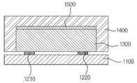
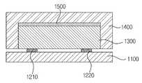
도 1은 본 발명의 일 실시예에 따른 발광 소자 패키지의 단면도.
도 2는 본 발명의 다른 실시예에 따른 발광 소자 패지의 단면도
도 3a 내지 도 3c는 도 1의 발광 소자 패키지의 세부 공정을 도시한 단면도.
도 4a 내지 도 4c는 도 2의 발광 소자 패키지의 세부 공정을 도시한 단면도.1 is a cross-sectional view of a light emitting device package according to an embodiment of the present invention;
2 is a cross-sectional view of a light emitting device package according to another embodiment of the present invention
FIGS. 3A to 3C are cross-sectional views illustrating a detailed process of the light emitting device package of FIG. 1;
4A to 4C are cross-sectional views illustrating a detailed process of the light emitting device package of FIG. 2;
이하, 본 발명의 바람직한 실시예를 첨부한 도면을 참조하여 설명하기로 한다.Hereinafter, preferred embodiments of the present invention will be described with reference to the accompanying drawings.
본 발명의 일 실시예에 따른 발광 소자 패키지는 도 1에 도시된 것처럼, 발광 다이오드 소자(1300), 회로 기판(1100), 형광체층(1400) 및 버퍼층(1500)을 포함하여 구성될 수 있다.The light emitting device package according to an embodiment of the present invention may include a light
여기에서, 발광 다이오드 소자(1300)는 소정 영역의 파장의 빛을 제공하며, 구체적으로, 발광 다이오드 소자(1300)는 청색 파장의 빛을 제공하는 발광 다이오드나 자외선 파장의 빛을 제공하는 발광 다이오드일 수 있다.Here, the light
한편, 발광 다이오드 소자(1300)의 하면에는 회로 기판(1100)과 전기적으로 연결되는 본딩 패드(1210, 1220)가 금속 물질로 형성되어 있으며, 이러한 회로 기판(1100)은 발광 다이오드 소자(1300)의 하부에 배치된다.On the other hand,
또한, 형광체층(1400)은 발광 다이오드 소자(1300)의 측면과 상면을 둘러싸며 배치되도록 캡(cap) 형상으로 형성되며, 측부의 두께 및 상부의 두께가 균일하게 형성되어 발광 다이오드 소자(1300)의 측면이나 상면에서 발광되는 빛의 파장을 변이시켜 발광 다이오드 소자(1300)가 제공하는 빛을 백색광으로 변환시킨다. 여기에서, 형광체층(1400)은 형광체와 실리콘 등에 의해 형성된다.The
한편, 버퍼층(1500)은 상기 발광 다이오드 소자의 상면과 상기 형광체층의 하면 사이에 배치되어, 상기 발광 다이오드 소자의 상면에서 발생되는 열이 상기 형광체층의 하면에 전달되는 것을 억제하는 동시에 상기 형광체층의 하면이 상기 발광 다이오드 소자의 상면에서 이탈되는 것을 억제한다.On the other hand, the
여기에서, 버퍼층(1500)은 상기 발광 다이오드 소자의 상면의 일부 또는 전부에만 코팅된 후에 상기 형광체층이 부착되는 것이 바람직하다.Here, it is preferable that the phosphor layer is attached after the
또한, 상기 버퍼층(1500)은 투명한 실리콘, 투명한 에폭시, 투명한 유기 폴리머, 또는 투명한 글래스 수지 중 적어도 어느 하나를 포함하여 형성되며, 5 ㎛ ~ 150 ㎛ 두께로 형성된다.In addition, the
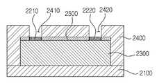
본 발명의 다른 실시예에 따른 발광 소자 패키지는 도 2에 도시된 것처럼, 발광 다이오드 소자(2300), 회로 기판(2100), 형광체층(2400) 및 버퍼층(2500)을 포함하여 구성될 수 있다.The light emitting device package according to another embodiment of the present invention may include a light
여기에서, 발광 다이오드 소자(2300)는 소정 영역의 파장의 빛을 제공하며, 구체적으로, 발광 다이오드 소자(2300)는 청색 파장의 빛을 제공하는 발광 다이오드나 자외선 파장의 빛을 제공하는 발광 다이오드일 수 있다.Here, the light
한편, 발광 다이오드 소자(2300)의 상면에는 회로 기판(2100)과 전기적으로 연결되는 본딩 패드(2210, 2220)가 금속 물질로 형성되어 있으며, 이러한 회로 기판(2100)은 발광 다이오드 소자(2300)의 하부에 배치된다.On the upper surface of the light
또한, 형광체층(2400)은 발광 다이오드 소자(2300)의 측면과 상면을 둘러싸며 배치되도록 캡(cap) 형상으로 형성되며, 측부의 두께 및 상부의 두께가 균일하게 형성되어 발광 다이오드 소자(2300)의 측면이나 상면에서 발광되는 빛의 파장을 변이시켜 발광 다이오드 소자(2300)가 제공하는 빛을 백색광으로 변환시킨다. 여기에서, 형광체층(2400)은 형광체와 실리콘 등에 의해 형성된다.The
여기에서, 형광체층(2400)이 발광 다이오드 소자(2300)의 측면과 상면을 둘러싸며 배치되는 경우에 도 2에 도시된 것처럼, 발광 다이오드 소자(2300)의 본딩 패드(2210, 2220)가 노출되도록 상기 형광체층(2400)의 상부에 본딩홀(2410, 2420)이 형성되어 있다.2, the
한편, 버퍼층(2500)은 상기 발광 다이오드 소자의 상면과 상기 형광체층의 하면 사이의 상기 본딩 패드가 형성된 영역을 제외한 영역에 배치되어, 상기 발광 다이오드 소자의 상면에서 발생되는 열이 상기 형광체층의 하면에 전달되는 것을 억제하는 동시에 상기 형광체층의 하면이 상기 발광 다이오드 소자의 상면에서 이탈되는 것을 억제한다.On the other hand, the
여기에서, 버퍼층(2500)은 상기 발광 다이오드 소자의 상면의 일부 또는 전부에만 코팅된 후에 상기 형광체층이 부착되는 것이 바람직하다.Here, it is preferable that the phosphor layer is attached after the
또한, 상기 버퍼층(2500)은 투명한 실리콘, 투명한 에폭시, 투명한 유기 폴리머, 또는 투명한 글래스 수지 중 적어도 어느 하나를 포함하여 형성되며, 5 ㎛ ~ 150 ㎛ 두께로 형성된다.In addition, the
본 발명의 실시예들에 따른 발광 소자 패키지에 채용되는 형광체층(1400, 2400)은 발광 다이오드 소자(1300, 2300)의 측면과 상면을 둘러싸며 배치되도록 캡(cap) 형상으로 형성되며, 측부의 두께 및 상부의 두께가 균일하게 형성됨으로써, 발광 다이오드 소자(1300, 2300)에서 발광되는 광원의 휘도 및 지향각을 증가시키면서도 색 균일도를 효과적으로 증가시킬 수 있다.The phosphor layers 1400 and 2400 employed in the light emitting device package according to the embodiments of the present invention are formed in a cap shape so as to surround the side surfaces and the upper surface of the light emitting
또한, 본 발명의 실시예들에 따른 발광 소자 패키지는 상술한 형광체층 상기 발광 다이오드 소자의 상면의 일부 또는 전부에만 코팅된 버퍼층(1500, 2500)에 부착시킴으로써 상술한 형광체층이 상기 발광 다이오드 소자의 발열에 의해서 열화되는 것을 효과적으로 억제할 수 있다.
In addition, the light emitting device package according to embodiments of the present invention may be formed by attaching the phosphor layer to the
이하에서는, 도 3a 내지 도 3c를 참조하여, 본 발명의 일 실시예에 따른 발광 다이오드 패키지의 제조 방법에 대해서 설명한다.Hereinafter, a method of manufacturing a light emitting diode package according to an embodiment of the present invention will be described with reference to FIGS. 3A to 3C. FIG.
먼저, 도 3a에 도시된 것처럼, 소정 영역의 파장의 빛을 제공하며, 하면에 본딩 패드(1210, 1220)가 형성되어 있는 발광 다이오드 소자(1300)를, 회로 기판(1100) 위에 마운트한다.First, as shown in FIG. 3A, a light emitting
다음으로, 도 3b에 도시된 것처럼, 상기 발광 다이오드 소자(1300)의 상면에, 상기 발광 다이오드 소자(1300)의 상면에서 발생되는 열이 상부로 전달되는 것을 억제하는 동시에 상기 발광 다이오드 소자(1300)의 상면에서 부착될 부품이 이탈되는 것을 억제하는 버퍼층(1500)을 코팅한다.3B, on the upper surface of the light emitting
다음으로, 도 3c에 도시된 것처럼, 캡(cap) 형상으로 형성되며, 측부의 두께 및 상부의 두께가 균일하게 형성된 형광체층(1400)이 상기 발광 다이오드 소자(1300)의 측면과 상면을 둘러싸며 배치되어, 상기 버퍼층(1500)의 상면에 부착된다.Next, as shown in FIG. 3C, a
이하에서는, 도 4a 내지 도 4c를 참조하여, 본 발명의 다른 실시예에 따른 발광 다이오드 패키지의 제조 방법에 대해서 설명한다.Hereinafter, a method for fabricating a light emitting diode package according to another embodiment of the present invention will be described with reference to FIGS. 4A to 4C. FIG.
먼저, 도 4a에 도시된 것처럼, 소정 영역의 파장의 빛을 제공하며, 상면에 본딩 패드(2210, 2220)가 형성되어 있는 발광 다이오드 소자(2300)를, 회로 기판(2100) 위에 마운트한다.First, as shown in FIG. 4A, a light emitting
다음으로, 도 4b에 도시된 것처럼, 상기 발광 다이오드 소자(2300)의 상면의 상기 본딩 패드(2210, 2220)가 형성된 영역을 제외한 영역에, 상기 발광 다이오드 소자(2300)의 상면에서 발생되는 열이 상부로 전달되는 것을 억제하는 동시에 상기 발광 다이오드 소자(2300)의 상면에 부착될 부품이 이탈되는 것을 억제하는 버퍼층(2500)을 코팅한다.4B, the heat generated from the upper surface of the light emitting
다음으로, 도 4c에 도시된 것처럼, 상기 발광 다이오드 소자(2300)의 측면과 상면을 둘러싸며 배치되도록 캡(cap) 형상으로 형성되며, 측부의 두께 및 상부의 두께가 균일하게 형성되고, 상기 발광 다이오드 소자(2300)의 본딩 패드가 노출되도록 상기 형광체층의 상부에 본딩홀(2410, 2420)이 형성된 형광체층(2400)이 상기 발광 다이오드 소자(2300)의 측면과 상면을 둘러싸며 배치되어, 상기 버퍼층(2500)의 상면에 부착되는 단계를 포함한다.Next, as shown in FIG. 4C, it is formed in a cap shape so as to surround the side surface and the upper surface of the light emitting
이상, 본 발명을 본 발명의 원리를 예시하기 위한 바람직한 실시예와 관련하여 설명하고 도시하였지만, 본 발명은 그와 같이 도시되고 설명된 그대로의 구성 및 작용으로 한정되는 것이 아니다. While the present invention has been particularly shown and described with reference to exemplary embodiments thereof, it is to be understood that the invention is not limited to the disclosed exemplary embodiments.
오히려, 첨부된 청구범위의 사상 및 범주를 일탈함이 없이 본 발명에 대한 다수의 변경 및 수정이 가능함을 당업자들은 잘 이해할 수 있을 것이다.
On the contrary, those skilled in the art will appreciate that many modifications and variations of the present invention are possible without departing from the spirit and scope of the appended claims.
따라서, 그러한 모든 적절한 변경 및 수정과 균등물들도 본 발명의 범위에 속하는 것으로 간주되어야 할 것이다.
Accordingly, all such appropriate modifications and changes, and equivalents thereof, should be regarded as within the scope of the present invention.
1100, 2100 : 회로 기판
1210, 1220, 2210, 2220 : 본딩 패드
1300, 2300 : 발광 다이오드 소자
1400, 2400 : 형광체층
1500, 2500 : 버퍼층
2410, 2420 : 본딩홀1100, 2100: circuit board
1210, 1220, 2210, 2220: bonding pads
1300, 2300: Light emitting diode element
1400, 2400: phosphor layer
1500, 2500: buffer layer
2410, 2420: bonding hole
Claims (16)
Translated fromKorean상기 발광 다이오드 소자의 하면에 형성되어 있는 본딩 패드를 통해서 상기 발광 다이오드 소자와 전기적으로 연결되는 회로 기판;
상기 발광 다이오드 소자의 측면과 상면을 둘러싸며 배치되도록 캡(cap) 형상으로 형성되며, 측부의 두께 및 상부의 두께가 균일하게 형성된 형광체층; 및
상기 발광 다이오드 소자의 상면과 상기 형광체층의 하면 사이에 배치되어, 상기 발광 다이오드 소자의 상면에서 발생되는 열이 상기 형광체층의 하면에 전달되는 것을 억제하는 동시에 상기 형광체층의 하면이 상기 발광 다이오드 소자의 상면에서 이탈되는 것을 억제하는 버퍼층을 포함하는 발광 다이오드 패키지.
A light emitting diode element for providing light of a wavelength of a predetermined region;
A circuit board electrically connected to the light emitting diode device through a bonding pad formed on a lower surface of the light emitting diode device;
A phosphor layer formed in a cap shape so as to surround the side surface and the upper surface of the light emitting diode, the thickness of the side portion being uniform and the thickness of the upper portion being uniform; And
Wherein the phosphor layer is disposed between the upper surface of the light emitting diode and the lower surface of the phosphor layer to prevent heat generated from the upper surface of the light emitting diode element from being transmitted to the lower surface of the phosphor layer, And a buffer layer for preventing the light emitting layer from being separated from the upper surface of the light emitting diode package.
상기 형광체층은 형광체와 실리콘에 의해 형성된 발광 소자 패키지.
The method according to claim 1,
Wherein the phosphor layer is formed of a phosphor and silicon.
상기 버퍼층은 투명한 실리콘, 투명한 에폭시, 투명한 유기 폴리머, 또는 투명한 글래스 수지 중 적어도 어느 하나를 포함하는 발광 소자 패키지.
The method according to claim 1,
Wherein the buffer layer comprises at least one of transparent silicon, transparent epoxy, transparent organic polymer, or transparent glass resin.
상기 버퍼층은 5 ㎛ ~ 150 ㎛ 두께로 형성된 발광 소자 패키지.
The method of claim 3,
Wherein the buffer layer is formed to a thickness of 5 mu m to 150 mu m.
상기 발광 다이오드 소자의 하부에 배치되며 상기 본딩 패드를 통해서 상기 발광 다이오드 소자와 전기적으로 연결되는 회로 기판; 및
상기 발광 다이오드 소자의 측면과 상면을 둘러싸며 배치되도록 캡(cap) 형상으로 형성되며, 측부의 두께 및 상부의 두께가 균일하게 형성된 형광체층을 포함하며,
상기 형광체층이 상기 발광 다이오드 소자의 측면과 상면을 둘러싸며 배치되는 경우에 상기 발광 다이오드 소자의 본딩 패드가 노출되도록 상기 형광체층의 상부에 본딩홀이 형성되어 있으며,
상기 발광 다이오드 소자의 상면과 상기 형광체층의 하면 사이의 상기 본딩 패드가 형성된 영역을 제외한 영역에 배치되어, 상기 발광 다이오드 소자의 상면에서 발생되는 열이 상기 형광체층의 하면에 전달되는 것을 억제하는 동시에 상기 형광체층의 하면이 상기 발광 다이오드 소자의 상면에서 이탈되는 것을 억제하는 버퍼층을 포함하는 발광 다이오드 패키지.
A light emitting diode element for providing light of a wavelength in a predetermined region and having a bonding pad formed on an upper surface thereof;
A circuit board disposed below the light emitting diode device and electrically connected to the light emitting diode device through the bonding pad; And
And a phosphor layer formed in a cap shape so as to surround the side surface and the upper surface of the light emitting diode, the thickness of the side portion and the thickness of the upper portion being uniformly formed,
A bonding hole is formed on the phosphor layer so that the bonding pad of the LED is exposed when the phosphor layer is disposed so as to surround the side surface and the upper surface of the LED,
The phosphor layer is disposed in a region between the upper surface of the light emitting diode and the lower surface of the phosphor layer except for the region where the bonding pad is formed to prevent the heat generated from the upper surface of the light emitting diode element from being transmitted to the lower surface of the phosphor layer And a buffer layer for preventing the lower surface of the phosphor layer from being separated from the upper surface of the light emitting diode element.
상기 형광체층은 형광체와 실리콘에 의해 형성된 발광 소자 패키지.
6. The method of claim 5,
Wherein the phosphor layer is formed of a phosphor and silicon.
상기 버퍼층은 투명한 실리콘, 투명한 에폭시, 투명한 유기 폴리머, 또는 투명한 글래스 수지 중 적어도 어느 하나를 포함하는 발광 소자 패키지.
6. The method of claim 5,
Wherein the buffer layer comprises at least one of transparent silicon, transparent epoxy, transparent organic polymer, or transparent glass resin.
상기 버퍼층은 5 ㎛ ~ 150 ㎛ 두께로 형성된 발광 소자 패키지.
8. The method of claim 7,
Wherein the buffer layer is formed to a thickness of 5 mu m to 150 mu m.
상기 발광 다이오드 소자의 상면에, 상기 발광 다이오드 소자의 상면에서 발생되는 열이 상부로 전달되는 것을 억제하는 동시에 상기 발광 다이오드 소자의 상면에서 부착될 부품이 이탈되는 것을 억제하는 버퍼층을 코팅하는 단계; 및
캡(cap) 형상으로 형성되며, 측부의 두께 및 상부의 두께가 균일하게 형성된 형광체층이 상기 발광 다이오드 소자의 측면과 상면을 둘러싸며 배치되어, 상기 버퍼층의 상면에 부착되는 단계를 포함하는 발광 다이오드 패키지의 제조 방법.
Mounting a light emitting diode device on a circuit board, the light emitting diode device providing light of a wavelength of a predetermined region and having a bonding pad formed on a lower surface thereof;
Coating a buffer layer on an upper surface of the light emitting diode device to suppress transfer of heat generated from an upper surface of the light emitting diode device to an upper portion of the light emitting diode device and to prevent a component to be attached from being detached from the upper surface of the light emitting diode device; And
Wherein a phosphor layer formed in a cap shape and having a thickness of a side portion and a thickness of an upper portion formed uniformly is disposed so as to surround a side surface and an upper surface of the light emitting diode element and attached to an upper surface of the buffer layer, A method of manufacturing a package.
상기 형광체층은 형광체와 실리콘에 의해 형성된 발광 소자 패키지.
10. The method of claim 9,
Wherein the phosphor layer is formed of a phosphor and silicon.
상기 버퍼층은 투명한 실리콘, 투명한 에폭시, 투명한 유기 폴리머, 또는 투명한 글래스 수지 중 적어도 어느 하나를 포함하는 발광 소자 패키지의 제조 방법.
10. The method of claim 9,
Wherein the buffer layer comprises at least one of transparent silicon, transparent epoxy, transparent organic polymer, or transparent glass resin.
상기 버퍼층은 5 ㎛ ~ 150 ㎛ 두께로 형성된 발광 소자 패키지의 제조 방법.
12. The method of claim 11,
Wherein the buffer layer has a thickness of 5 to 150 탆.
상기 발광 다이오드 소자의 상면의 상기 본딩 패드가 형성된 영역을 제외한 영역에, 상기 발광 다이오드 소자의 상면에서 발생되는 열이 상부로 전달되는 것을 억제하는 동시에 상기 발광 다이오드 소자의 상면에 부착될 부품이 이탈되는 것을 억제하는 버퍼층을 코팅하는 단계; 및
상기 발광 다이오드 소자의 측면과 상면을 둘러싸며 배치되도록 캡(cap) 형상으로 형성되며, 측부의 두께 및 상부의 두께가 균일하게 형성되고, 상기 발광 다이오드 소자의 본딩 패드가 노출되도록 상기 형광체층의 상부에 본딩홀이 형성된 형광체층이 상기 발광 다이오드 소자의 측면과 상면을 둘러싸며 배치되어, 상기 버퍼층의 상면에 부착되는 단계를 포함하는 발광 다이오드 패키지의 제조 방법.
Mounting a light emitting diode device on a circuit board, the light emitting diode device providing light of a predetermined wavelength and having a bonding pad on an upper surface thereof;
The heat generated in the upper surface of the light emitting diode device is prevented from being transferred to the upper portion of the upper surface of the light emitting diode device except for the region where the bonding pad is formed and the part to be attached to the upper surface of the light emitting diode device is removed Coating a buffer layer on the substrate; And
The light emitting diode device according to the present invention is characterized in that the light emitting diode device is formed in a cap shape so as to surround the side surface and the upper surface of the light emitting diode device and the thickness of the side portion and the thickness of the upper portion are uniformly formed, Wherein a phosphor layer having a bonding hole formed therein is disposed on a side surface and an upper surface of the light emitting diode, and the phosphor layer is attached to an upper surface of the buffer layer.
상기 형광체층은 형광체와 실리콘에 의해 형성된 발광 소자 패키지.
14. The method of claim 13,
Wherein the phosphor layer is formed of a phosphor and silicon.
상기 버퍼층은 투명한 실리콘, 투명한 에폭시, 투명한 유기 폴리머, 또는 투명한 글래스 수지 중 적어도 어느 하나를 포함하는 발광 소자 패키지의 제조 방법.
14. The method of claim 13,
Wherein the buffer layer comprises at least one of transparent silicon, transparent epoxy, transparent organic polymer, or transparent glass resin.
상기 버퍼층은 5 ㎛ ~ 150 ㎛ 두께로 형성된 발광 소자 패키지의 제조 방법.
16. The method of claim 15,
Wherein the buffer layer has a thickness of 5 to 150 탆.
Priority Applications (2)
| Application Number | Priority Date | Filing Date | Title |
|---|---|---|---|
| KR1020140048553AKR20150122360A (en) | 2014-04-23 | 2014-04-23 | Package for Light Emitting Device and Method for Manufacturing thereof |
| US14/609,777US9929309B2 (en) | 2014-04-23 | 2015-01-30 | Light-emitting diode package and method of manufacturing the same |
Applications Claiming Priority (1)
| Application Number | Priority Date | Filing Date | Title |
|---|---|---|---|
| KR1020140048553AKR20150122360A (en) | 2014-04-23 | 2014-04-23 | Package for Light Emitting Device and Method for Manufacturing thereof |
Related Child Applications (1)
| Application Number | Title | Priority Date | Filing Date |
|---|---|---|---|
| KR1020150162324ADivisionKR20150136041A (en) | 2015-11-19 | 2015-11-19 | Package for Light Emitting Device and Method for Manufacturing thereof |
Publications (1)
| Publication Number | Publication Date |
|---|---|
| KR20150122360Atrue KR20150122360A (en) | 2015-11-02 |
Family
ID=54335569
Family Applications (1)
| Application Number | Title | Priority Date | Filing Date |
|---|---|---|---|
| KR1020140048553ACeasedKR20150122360A (en) | 2014-04-23 | 2014-04-23 | Package for Light Emitting Device and Method for Manufacturing thereof |
Country Status (2)
| Country | Link |
|---|---|
| US (1) | US9929309B2 (en) |
| KR (1) | KR20150122360A (en) |
Families Citing this family (3)
| Publication number | Priority date | Publication date | Assignee | Title |
|---|---|---|---|---|
| KR20160050341A (en)* | 2014-10-29 | 2016-05-11 | (주)라이타이저코리아 | Package for Light Emitting Device and Method for Manufacturing thereof |
| US10559727B2 (en)* | 2017-07-25 | 2020-02-11 | Shenzhen China Star Optoelectronics Semiconductor Display Technology Co., Ltd. | Manufacturing method of colorful Micro-LED, display modlue and terminals |
| CN111477732B (en) | 2019-01-24 | 2021-10-08 | 隆达电子股份有限公司 | Light emitting device |
Family Cites Families (9)
| Publication number | Priority date | Publication date | Assignee | Title |
|---|---|---|---|---|
| AT410266B (en)* | 2000-12-28 | 2003-03-25 | Tridonic Optoelectronics Gmbh | LIGHT SOURCE WITH A LIGHT-EMITTING ELEMENT |
| US6841802B2 (en)* | 2002-06-26 | 2005-01-11 | Oriol, Inc. | Thin film light emitting diode |
| DE10259945A1 (en)* | 2002-12-20 | 2004-07-01 | Tews, Walter, Dipl.-Chem. Dr.rer.nat.habil. | Phosphors with an extended fluorescence lifetime |
| US7858408B2 (en)* | 2004-11-15 | 2010-12-28 | Koninklijke Philips Electronics N.V. | LED with phosphor tile and overmolded phosphor in lens |
| US7692207B2 (en)* | 2005-01-21 | 2010-04-06 | Luminus Devices, Inc. | Packaging designs for LEDs |
| US7671468B2 (en)* | 2005-09-30 | 2010-03-02 | Tdk Corporation | Light emitting apparatus |
| KR101144634B1 (en) | 2007-01-25 | 2012-05-08 | 서울반도체 주식회사 | Phosphor light emitting diode and method for manufacturing the same |
| KR20110051769A (en) | 2009-11-11 | 2011-05-18 | 삼성엘이디 주식회사 | Manufacturing method of light emitting device package |
| KR101253586B1 (en) | 2010-08-25 | 2013-04-11 | 삼성전자주식회사 | Phosphor film, method of manufacturing the same, method of coating phosphor layer on an LED chip, method of manufacturing LED package and LED package manufactured thereof |
- 2014
- 2014-04-23KRKR1020140048553Apatent/KR20150122360A/ennot_activeCeased
- 2015
- 2015-01-30USUS14/609,777patent/US9929309B2/enactiveActive
Also Published As
| Publication number | Publication date |
|---|---|
| US20150311408A1 (en) | 2015-10-29 |
| US9929309B2 (en) | 2018-03-27 |
Similar Documents
| Publication | Publication Date | Title |
|---|---|---|
| JP6186904B2 (en) | Light emitting device | |
| TWI604239B (en) | Color conversion substrate, method of fabricating the same, and display device including the same | |
| US7888698B2 (en) | Photoelectric semiconductor device capable of generating uniform compound lights | |
| US8545082B2 (en) | Light emitting apparatus and lighting system | |
| EP2819189B1 (en) | Method and hardware to enhance light out-coupling | |
| US20120268007A1 (en) | LED Light Source and Chromaticity Adjustment Method for LED Light Source | |
| WO2011084001A2 (en) | Aspheric led lens and a light emitting device including the same | |
| JP2008251663A (en) | Light emitting device and lighting device | |
| JP6485503B2 (en) | Method for manufacturing light emitting device | |
| KR20120079666A (en) | The light- | |
| US9733514B2 (en) | Light emitting diode light source, manufacturing method thereof, backlight source and display device | |
| KR20150122360A (en) | Package for Light Emitting Device and Method for Manufacturing thereof | |
| WO2010074479A3 (en) | Led package, method for manufacturing an led package, backlight unit, and lighting apparatus | |
| KR101641205B1 (en) | The manufacturing method for LED light module contained adjustable Emitting angle | |
| KR20170045851A (en) | Package for Light Emitting Device and Method for Manufacturing thereof | |
| US8878208B2 (en) | Illuminating device | |
| KR101212654B1 (en) | Package for light emitting diode and method for manufacturing thereof | |
| KR101847916B1 (en) | Led display apparatus and method for manufacturing the same | |
| US9871174B2 (en) | Light-emitting device | |
| US20200035657A1 (en) | Electroluminescent device and method of manufacturing the same | |
| KR20170043839A (en) | Package for Light Emitting Device and Method for Manufacturing thereof | |
| KR20150136041A (en) | Package for Light Emitting Device and Method for Manufacturing thereof | |
| KR20170003182A (en) | Light emitting diode | |
| KR101616474B1 (en) | Package for Light Emitting Device and Method for Manufacturing thereof | |
| KR20150092597A (en) | Light emitting device package and lighting apparatus including the same |
Legal Events
| Date | Code | Title | Description |
|---|---|---|---|
| A201 | Request for examination | ||
| PA0109 | Patent application | Patent event code:PA01091R01D Comment text:Patent Application Patent event date:20140423 | |
| PA0201 | Request for examination | ||
| E902 | Notification of reason for refusal | ||
| PE0902 | Notice of grounds for rejection | Comment text:Notification of reason for refusal Patent event date:20150408 Patent event code:PE09021S01D | |
| E601 | Decision to refuse application | ||
| PE0601 | Decision on rejection of patent | Patent event date:20151021 Comment text:Decision to Refuse Application Patent event code:PE06012S01D Patent event date:20150408 Comment text:Notification of reason for refusal Patent event code:PE06011S01I | |
| PG1501 | Laying open of application | ||
| A107 | Divisional application of patent | ||
| PA0107 | Divisional application | Comment text:Divisional Application of Patent Patent event date:20151119 Patent event code:PA01071R01D |