KR20150120376A - Peeling method, semiconductor device, and peeling apparatus - Google Patents
Peeling method, semiconductor device, and peeling apparatusDownload PDFInfo
- Publication number
- KR20150120376A KR20150120376AKR1020157022581AKR20157022581AKR20150120376AKR 20150120376 AKR20150120376 AKR 20150120376AKR 1020157022581 AKR1020157022581 AKR 1020157022581AKR 20157022581 AKR20157022581 AKR 20157022581AKR 20150120376 AKR20150120376 AKR 20150120376A
- Authority
- KR
- South Korea
- Prior art keywords
- layer
- peeling
- nitrogen
- roller
- oxide
- Prior art date
- Legal status (The legal status is an assumption and is not a legal conclusion. Google has not performed a legal analysis and makes no representation as to the accuracy of the status listed.)
- Ceased
Links
Images


Classifications
- H—ELECTRICITY
- H01—ELECTRIC ELEMENTS
- H01L—SEMICONDUCTOR DEVICES NOT COVERED BY CLASS H10
- H01L21/00—Processes or apparatus adapted for the manufacture or treatment of semiconductor or solid state devices or of parts thereof
- H01L21/67—Apparatus specially adapted for handling semiconductor or electric solid state devices during manufacture or treatment thereof; Apparatus specially adapted for handling wafers during manufacture or treatment of semiconductor or electric solid state devices or components ; Apparatus not specifically provided for elsewhere
- H01L21/67005—Apparatus not specifically provided for elsewhere
- H01L21/67011—Apparatus for manufacture or treatment
- H01L21/67132—Apparatus for placing on an insulating substrate, e.g. tape
- H—ELECTRICITY
- H01—ELECTRIC ELEMENTS
- H01L—SEMICONDUCTOR DEVICES NOT COVERED BY CLASS H10
- H01L21/00—Processes or apparatus adapted for the manufacture or treatment of semiconductor or solid state devices or of parts thereof
- H01L21/67—Apparatus specially adapted for handling semiconductor or electric solid state devices during manufacture or treatment thereof; Apparatus specially adapted for handling wafers during manufacture or treatment of semiconductor or electric solid state devices or components ; Apparatus not specifically provided for elsewhere
- H01L21/683—Apparatus specially adapted for handling semiconductor or electric solid state devices during manufacture or treatment thereof; Apparatus specially adapted for handling wafers during manufacture or treatment of semiconductor or electric solid state devices or components ; Apparatus not specifically provided for elsewhere for supporting or gripping
- H01L21/6835—Apparatus specially adapted for handling semiconductor or electric solid state devices during manufacture or treatment thereof; Apparatus specially adapted for handling wafers during manufacture or treatment of semiconductor or electric solid state devices or components ; Apparatus not specifically provided for elsewhere for supporting or gripping using temporarily an auxiliary support
- H01L21/6836—Wafer tapes, e.g. grinding or dicing support tapes
- H01L51/003—
- H01L51/0097—
- H01L51/50—
- H—ELECTRICITY
- H10—SEMICONDUCTOR DEVICES; ELECTRIC SOLID-STATE DEVICES NOT OTHERWISE PROVIDED FOR
- H10D—INORGANIC ELECTRIC SEMICONDUCTOR DEVICES
- H10D30/00—Field-effect transistors [FET]
- H10D30/60—Insulated-gate field-effect transistors [IGFET]
- H10D30/67—Thin-film transistors [TFT]
- H—ELECTRICITY
- H10—SEMICONDUCTOR DEVICES; ELECTRIC SOLID-STATE DEVICES NOT OTHERWISE PROVIDED FOR
- H10K—ORGANIC ELECTRIC SOLID-STATE DEVICES
- H10K71/00—Manufacture or treatment specially adapted for the organic devices covered by this subclass
- H10K71/80—Manufacture or treatment specially adapted for the organic devices covered by this subclass using temporary substrates
- B—PERFORMING OPERATIONS; TRANSPORTING
- B32—LAYERED PRODUCTS
- B32B—LAYERED PRODUCTS, i.e. PRODUCTS BUILT-UP OF STRATA OF FLAT OR NON-FLAT, e.g. CELLULAR OR HONEYCOMB, FORM
- B32B38/00—Ancillary operations in connection with laminating processes
- B32B38/10—Removing layers, or parts of layers, mechanically or chemically
- H—ELECTRICITY
- H01—ELECTRIC ELEMENTS
- H01L—SEMICONDUCTOR DEVICES NOT COVERED BY CLASS H10
- H01L2221/00—Processes or apparatus adapted for the manufacture or treatment of semiconductor or solid state devices or of parts thereof covered by H01L21/00
- H01L2221/67—Apparatus for handling semiconductor or electric solid state devices during manufacture or treatment thereof; Apparatus for handling wafers during manufacture or treatment of semiconductor or electric solid state devices or components; Apparatus not specifically provided for elsewhere
- H01L2221/683—Apparatus for handling semiconductor or electric solid state devices during manufacture or treatment thereof; Apparatus for handling wafers during manufacture or treatment of semiconductor or electric solid state devices or components; Apparatus not specifically provided for elsewhere for supporting or gripping
- H01L2221/68304—Apparatus for handling semiconductor or electric solid state devices during manufacture or treatment thereof; Apparatus for handling wafers during manufacture or treatment of semiconductor or electric solid state devices or components; Apparatus not specifically provided for elsewhere for supporting or gripping using temporarily an auxiliary support
- H01L2221/68318—Auxiliary support including means facilitating the separation of a device or wafer from the auxiliary support
- H—ELECTRICITY
- H01—ELECTRIC ELEMENTS
- H01L—SEMICONDUCTOR DEVICES NOT COVERED BY CLASS H10
- H01L2221/00—Processes or apparatus adapted for the manufacture or treatment of semiconductor or solid state devices or of parts thereof covered by H01L21/00
- H01L2221/67—Apparatus for handling semiconductor or electric solid state devices during manufacture or treatment thereof; Apparatus for handling wafers during manufacture or treatment of semiconductor or electric solid state devices or components; Apparatus not specifically provided for elsewhere
- H01L2221/683—Apparatus for handling semiconductor or electric solid state devices during manufacture or treatment thereof; Apparatus for handling wafers during manufacture or treatment of semiconductor or electric solid state devices or components; Apparatus not specifically provided for elsewhere for supporting or gripping
- H01L2221/68304—Apparatus for handling semiconductor or electric solid state devices during manufacture or treatment thereof; Apparatus for handling wafers during manufacture or treatment of semiconductor or electric solid state devices or components; Apparatus not specifically provided for elsewhere for supporting or gripping using temporarily an auxiliary support
- H01L2221/6835—Apparatus for handling semiconductor or electric solid state devices during manufacture or treatment thereof; Apparatus for handling wafers during manufacture or treatment of semiconductor or electric solid state devices or components; Apparatus not specifically provided for elsewhere for supporting or gripping using temporarily an auxiliary support used as a support during build up manufacturing of active devices
- H—ELECTRICITY
- H01—ELECTRIC ELEMENTS
- H01L—SEMICONDUCTOR DEVICES NOT COVERED BY CLASS H10
- H01L2221/00—Processes or apparatus adapted for the manufacture or treatment of semiconductor or solid state devices or of parts thereof covered by H01L21/00
- H01L2221/67—Apparatus for handling semiconductor or electric solid state devices during manufacture or treatment thereof; Apparatus for handling wafers during manufacture or treatment of semiconductor or electric solid state devices or components; Apparatus not specifically provided for elsewhere
- H01L2221/683—Apparatus for handling semiconductor or electric solid state devices during manufacture or treatment thereof; Apparatus for handling wafers during manufacture or treatment of semiconductor or electric solid state devices or components; Apparatus not specifically provided for elsewhere for supporting or gripping
- H01L2221/68304—Apparatus for handling semiconductor or electric solid state devices during manufacture or treatment thereof; Apparatus for handling wafers during manufacture or treatment of semiconductor or electric solid state devices or components; Apparatus not specifically provided for elsewhere for supporting or gripping using temporarily an auxiliary support
- H01L2221/68363—Apparatus for handling semiconductor or electric solid state devices during manufacture or treatment thereof; Apparatus for handling wafers during manufacture or treatment of semiconductor or electric solid state devices or components; Apparatus not specifically provided for elsewhere for supporting or gripping using temporarily an auxiliary support used in a transfer process involving transfer directly from an origin substrate to a target substrate without use of an intermediate handle substrate
- H—ELECTRICITY
- H01—ELECTRIC ELEMENTS
- H01L—SEMICONDUCTOR DEVICES NOT COVERED BY CLASS H10
- H01L2221/00—Processes or apparatus adapted for the manufacture or treatment of semiconductor or solid state devices or of parts thereof covered by H01L21/00
- H01L2221/67—Apparatus for handling semiconductor or electric solid state devices during manufacture or treatment thereof; Apparatus for handling wafers during manufacture or treatment of semiconductor or electric solid state devices or components; Apparatus not specifically provided for elsewhere
- H01L2221/683—Apparatus for handling semiconductor or electric solid state devices during manufacture or treatment thereof; Apparatus for handling wafers during manufacture or treatment of semiconductor or electric solid state devices or components; Apparatus not specifically provided for elsewhere for supporting or gripping
- H01L2221/68304—Apparatus for handling semiconductor or electric solid state devices during manufacture or treatment thereof; Apparatus for handling wafers during manufacture or treatment of semiconductor or electric solid state devices or components; Apparatus not specifically provided for elsewhere for supporting or gripping using temporarily an auxiliary support
- H01L2221/68381—Details of chemical or physical process used for separating the auxiliary support from a device or wafer
- H01L2221/68386—Separation by peeling
- H—ELECTRICITY
- H10—SEMICONDUCTOR DEVICES; ELECTRIC SOLID-STATE DEVICES NOT OTHERWISE PROVIDED FOR
- H10K—ORGANIC ELECTRIC SOLID-STATE DEVICES
- H10K50/00—Organic light-emitting devices
- H—ELECTRICITY
- H10—SEMICONDUCTOR DEVICES; ELECTRIC SOLID-STATE DEVICES NOT OTHERWISE PROVIDED FOR
- H10K—ORGANIC ELECTRIC SOLID-STATE DEVICES
- H10K77/00—Constructional details of devices covered by this subclass and not covered by groups H10K10/80, H10K30/80, H10K50/80 or H10K59/80
- H10K77/10—Substrates, e.g. flexible substrates
- H10K77/111—Flexible substrates
- Y—GENERAL TAGGING OF NEW TECHNOLOGICAL DEVELOPMENTS; GENERAL TAGGING OF CROSS-SECTIONAL TECHNOLOGIES SPANNING OVER SEVERAL SECTIONS OF THE IPC; TECHNICAL SUBJECTS COVERED BY FORMER USPC CROSS-REFERENCE ART COLLECTIONS [XRACs] AND DIGESTS
- Y10—TECHNICAL SUBJECTS COVERED BY FORMER USPC
- Y10T—TECHNICAL SUBJECTS COVERED BY FORMER US CLASSIFICATION
- Y10T156/00—Adhesive bonding and miscellaneous chemical manufacture
- Y10T156/17—Surface bonding means and/or assemblymeans with work feeding or handling means
- Y10T156/1702—For plural parts or plural areas of single part
- Y10T156/1712—Indefinite or running length work
Landscapes
- Engineering & Computer Science (AREA)
- Manufacturing & Machinery (AREA)
- Physics & Mathematics (AREA)
- Condensed Matter Physics & Semiconductors (AREA)
- General Physics & Mathematics (AREA)
- Computer Hardware Design (AREA)
- Microelectronics & Electronic Packaging (AREA)
- Power Engineering (AREA)
- Thin Film Transistor (AREA)
- Electroluminescent Light Sources (AREA)
Abstract
Translated fromKorean
Description
Translated fromKorean본 발명은 물건, 방법, 또는 제작 방법에 관한 것이다. 또한, 본 발명은 공정(process), 기계(machine), 제품(manufacture), 또는 조성물(composition of matter)에 관한 것이다. 특히, 본 발명의 일 형태는 반도체 장치, 표시 장치, 발광 장치, 이들의 구동 방법, 또는 이들의 제작 방법에 관한 것이다. 특히, 본 발명의 일 형태는 플렉시블 디바이스의 제작 방법에 관한 것이다.The present invention relates to an object, a method, or a manufacturing method. The invention also relates to a process, a machine, a manufacture, or a composition of matter. In particular, one aspect of the present invention relates to a semiconductor device, a display device, a light emitting device, a driving method thereof, or a manufacturing method thereof. Particularly, one aspect of the present invention relates to a manufacturing method of a flexible device.
근년, 가요성 기판 위에 반도체 소자 및 발광 소자 등이 제공된 플렉시블 디바이스가 개발되고 있다. 플렉시블 디바이스의 대표적인 예로서는, 조명 장치 및 화상 표시 장치 외에, 트랜지스터 등의 반도체 소자를 포함하는 다양한 반도체 회로를 들 수 있다.In recent years, flexible devices provided with semiconductor elements, light emitting elements, and the like on a flexible substrate have been developed. Representative examples of the flexible device include various semiconductor circuits including a semiconductor device such as a transistor in addition to a lighting device and an image display device.
가요성 기판을 포함하는 반도체 장치의 제작 방법으로서는, 유리 기판이나 석영 기판 등의 지지 기판 위에 박막 트랜지스터 등의 반도체 소자를 형성한 후, 가요성 기판에 반도체 소자를 전치(transfer)하는 기술이 개발되고 있다. 이 기술에서는, 반도체 소자를 포함한 층을 지지 기판으로부터 박리하는 공정이 필요하다.As a method for manufacturing a semiconductor device including a flexible substrate, a technique has been developed in which a semiconductor element such as a thin film transistor is formed on a support substrate such as a glass substrate or a quartz substrate, and then a semiconductor element is transferred onto a flexible substrate have. In this technique, a step of peeling the layer including the semiconductor element from the support substrate is required.
예를 들어, 특허문헌 1에는 레이저 어블레이션(laser ablation)을 사용한 다음의 박리 기술이 개시(開示)되어 있다. 기판 위에 비정질 실리콘 등으로 형성되는 분리층을 형성하고, 분리층 위에 박막 소자로 형성되는 피박리층을 형성하고, 박리된 층을 접착층을 사용하여 전사체(transfer body)에 접착시킨다. 레이저 광 조사에 의하여 분리층을 제거(ablate)함으로써, 분리층에서 박리가 생기게 한다.For example,
또한, 특허문헌 2에는 다음의 박리 기술이 개시되어 있다. 기판과 산화물층 사이에 금속층을 형성하고, 산화물층과 금속층의 계면의 결합이 약한 것을 이용하여 산화물층과 금속층의 계면에서 박리가 생기게 함으로써, 피박리층과 기판을 서로 분리한다.Further,
반도체 소자를 지지 기판으로부터 박리할 때에 박리 계면에서 박리가 어렵거나 박리성이 낮으면, 반도체 소자에 큰 응력이 가해져, 반도체 소자를 파괴하는 경우가 있다.If separation of the semiconductor element from the support substrate is difficult at the peeling interface or the peeling property is low, a large stress is applied to the semiconductor element and the semiconductor element may be broken.
상술한 것을 감안하여, 본 발명의 일 형태의 목적은 박리성이 향상된 박리 방법 등을 제공하는 것이다. 다른 목적은 박리 공정에서의 수율을 높이는 것이다. 다른 목적은 플렉시블 디바이스 등을 제작함에 있어서의 수율을 높이는 것이다. 다른 목적은 신뢰성이 높은 반도체 장치 등을 제공하는 것이다. 다른 목적은 가요성 기판이 제공되며 신뢰성이 높은 반도체 장치를 제공하는 것이다. 다른 목적은 신규 반도체 장치 등을 제공하는 것이다. 다른 목적은 신규 반도체 장치 등의 제작 방법을 제공하는 것이다. 또한, 이들 목적의 기재는 다른 목적들의 존재를 방해하지 않는다. 본 발명의 일 형태에서는, 이들 목적 모두를 달성할 필요는 없다. 다른 목적들은, 명세서, 도면, 청구항 등의 기재로부터 명백해지며 추출될 수 있다.SUMMARY OF THE INVENTION In view of the above, an object of one embodiment of the present invention is to provide a peeling method and the like with improved peelability. Another purpose is to increase the yield in the stripping process. Another object is to increase the yield in manufacturing a flexible device or the like. Another object is to provide a highly reliable semiconductor device or the like. Another object is to provide a highly reliable semiconductor device provided with a flexible substrate. Another object is to provide a novel semiconductor device or the like. Another object is to provide a method of manufacturing a novel semiconductor device or the like. In addition, the description of these objects does not preclude the presence of other objects. In an aspect of the present invention, it is not necessary to achieve all of these objects. Other objects can be extracted and extracted from the description of the specification, drawings, claims, and the like.
본 발명의 일 형태는 텅스텐을 포함하는 박리층을 지지 기판 위에 형성하는 제 1 공정; 박리층 위에, 산화질화 실리콘을 포함하는 제 1 층과 질화 실리콘을 포함하는 제 2 층이 순차적으로 적층된 피박리층, 및 박리층과 피박리층 사이에 산화 텅스텐을 포함하는 산화물층을 형성하는 제 2 공정; 가열 처리에 의하여 산화물층 내에 텅스텐과 질소를 포함하는 화합물을 형성하는 제 3 공정; 및 산화물층에서 피박리층으로부터 박리층을 박리하는 제 4 공정을 포함하는 박리 방법이다.One aspect of the present invention is a method of manufacturing a semiconductor device, comprising: a first step of forming a release layer including tungsten on a support substrate; A release layer on which a first layer containing silicon oxynitride and a second layer containing silicon nitride are sequentially laminated on the release layer and an oxide layer containing tungsten oxide between the release layer and the release layer A second step; A third step of forming a compound containing tungsten and nitrogen in the oxide layer by a heat treatment; And a fourth step of peeling the release layer from the layer to be peeled off from the oxide layer.
또한, 제 1 공정과 제 2 공정 사이에, 일산화 이질소를 포함하는 분위기에서 박리층의 표면에 플라즈마 처리를 수행하는 제 5 공정을 수행하는 것이 바람직하다.Between the first step and the second step, it is preferable to carry out the fifth step of performing the plasma treatment on the surface of the release layer in an atmosphere containing nitrogen monoxide.
제 2 공정에 있어서, SIMS(secondary ion mass spectrometry)에 의하여 측정되는 질소 함유량이 5.0×10²⁰분자/cm3 이상 1.0×10²³분자/cm3 이하인 영역과, 수소 함유량이 1.0×10²⁰분자/cm3 이상 1.0×10²²분자/cm3 이하인 영역을 포함한 산화질화 실리콘을 포함하는 제 1 층을 형성하는 것이 바람직하다.In the second step, a region where the nitrogen content measured by SIMS (secondary ion mass spectrometry) is 5.0 x 10²⁰ molecules / cm3 or more and 1.0 x 10²³ molecules / cm3 or less and a region where the hydrogen content is 1.0 x 10²⁰ molecules / cm <3 > and 1.0 x 10 <22 > molecules / cm <3 > or less.
제 2 공정에 있어서, 질량전하비(mass-to-charge ratio) 28에서의 TDS(thermal desorption spectrometry)에 의하여 얻어지는 스펙트럼에서, 100℃~450℃의 온도 범위에서 산화질화 실리콘으로부터 방출되는 질소의 양이, 질소 분자로 환산하였을 때 5×10¹⁷분자/cm3 이상이고, 질량전하비 2에서의 TDS에 의하여 얻어지는 스펙트럼에서, 100℃~450℃의 온도 범위에서 산화질화 실리콘으로부터 방출되는 수소의 양이, 수소 분자로 환산하였을 때 5×10¹⁹분자/cm3 이상인 산화질화 실리콘을 포함하는 제 1 층을 형성하는 것이 바람직하다.In the second step, in the spectrum obtained by TDS (thermal desorption spectrometry) at a mass-to-charge ratio of 28, the amount of nitrogen released from the silicon oxynitride in the temperature range of 100 ° C to 450 ° C is, 5 × 10¹⁷ molecules / cm3 or more, in a spectrum obtained by the TDS of the mass-
또한 제 2 공정에 있어서, 질량전하비 28에서의 TDS에 의하여 얻어지는 스펙트럼에서, 100℃~450℃의 온도 범위에서 질화 실리콘으로부터 방출되는 질소의 양이, 질소 분자로 환산하였을 때 5×10¹⁹분자/cm3 이하이고, 질량전하비 2에서의 TDS에 의하여 얻어지는 스펙트럼에서, 100℃~450℃의 온도 범위에서 질화 실리콘으로부터 방출되는 수소의 양이, 수소 분자로 환산하였을 때 1×10²⁰분자/cm3 이상인 질화 실리콘을 포함하는 제 2 층을 형성하는 것이 바람직하다.When the amount of nitrogen released from the silicon nitride in the temperature range of 100 ° C to 450 ° C in the spectrum obtained by the TDS at the
제 4 공정에서, 박리층과 피박리층 사이에 물 또는 수용액을 침투시키면서 박리를 수행하는 것이 바람직하다.In the fourth step, it is preferable to carry out peeling while allowing water or an aqueous solution to permeate between the peeling layer and the layer to be peeled.
본 발명의 다른 일 형태는, 가요성 기판 위의 접착층, 접착층 위의 산화 텅스텐을 포함하는 산화물층, 산화물층 위의 산화질화 실리콘을 포함하는 제 1 층, 제 1 층 위의 질화 실리콘을 포함하는 제 2 층, 및 제 2 층 위의 트랜지스터를 포함하는 반도체 장치이다. 산화물층은, SIMS에 의하여 측정되는 질소 함유량이 제 1 층보다 높은 영역과 SIMS에 의하여 측정되는 수소 함유량이 제 1 층보다 높은 영역을 포함한다.Another aspect of the present invention is a method of manufacturing a semiconductor device comprising the steps of: forming an adhesive layer over a flexible substrate, an oxide layer comprising tungsten oxide over the adhesive layer, a first layer comprising silicon oxynitride over the oxide layer, A second layer, and a transistor over the second layer. The oxide layer includes a region where the nitrogen content measured by SIMS is higher than the first layer and a region where the hydrogen content measured by SIMS is higher than the first layer.
상술한 반도체 장치에서, SIMS에 의하여 측정되는 제 1 층의 질소 및 수소의 농도는, 제 2 층 측으로부터 산화물층 측으로 갈수록 저하되는 것이 바람직하다.In the above-described semiconductor device, it is preferable that the concentration of nitrogen and hydrogen in the first layer measured by SIMS decrease from the second layer side toward the oxide layer side.
본 발명에 따르면, 박리성이 향상된 박리 방법을 제공할 수 있다. 또한, 박리 공정에서의 수율을 높일 수 있다. 또한, 플렉시블 디바이스를 제작함에 있어서의 수율을 높일 수 있다. 또한, 신뢰성이 높은 반도체 장치를 제공할 수 있다. 또한, 가요성 기판이 제공되며 신뢰성이 높은 반도체 장치를 제공할 수 있다.According to the present invention, it is possible to provide a peeling method with improved peelability. In addition, the yield in the peeling step can be increased. In addition, the yield in manufacturing a flexible device can be increased. Further, a highly reliable semiconductor device can be provided. In addition, a highly reliable semiconductor device provided with a flexible substrate can be provided.
도 1의 (A)~(E)는 실시형태에 따른 박리 방법을 도시한 도면.
도 2의 (A) 및 (B)는 실시형태에 따른 박리 방법을 도시한 도면.
도 3의 (A) 및 (B)는 실시형태에 따른 표시 장치의 구성예를 도시한 도면.
도 4는 실시형태에 따른 표시 장치의 구성예를 도시한 도면.
도 5의 (A) 및 (B)는 실시형태에 따른 발광 장치의 구성예를 도시한 도면.
도 6의 (A) 및 (B)는 실시형태에 따른 계산에 사용되는 모델을 도시한 도면.
도 7은 실시형태에 따른 결합 에너지의 계산 결과를 나타낸 도면.
도 8은 실시형태에 따른 결합 에너지의 계산 결과를 나타낸 도면.
도 9는 실시형태에 따른 결합 에너지의 계산 결과를 나타낸 도면.
도 10은 실시형태에 따른 박리 시험에 사용되는 장치의 구성예를 도시한 도면.
도 11은 실시형태에 따른 박리에 사용되는 용액의 종류와 박리성의 관계를 나타낸 도면.
도 12의 (A)~(C)는 실시형태에 따른 계산에 사용되는 모델을 나타낸 도면.
도 13의 (A) 및 (B)는 실시형태에 따른 가교 구조의 계산 결과를 나타낸 도면.
도 14의 (A) 및 (B)는 실시형태에 따른 가교 구조의 계산 결과를 나타낸 도면.
도 15는 실시형태에 따른 에너지 다이어그램의 계산 결과를 나타낸 도면.
도 16은 실시형태에 따른 박리 장치의 구성예를 도시한 도면.
도 17의 (A)~(E)는 실시형태에 따른 박리 방법을 도시한 도면.
도 18의 (A)~(C)는 실시형태에 따른 박리 방법을 도시한 도면.
도 19의 (A) 및 (B)는 실시형태에 따른 박리 방법을 도시한 도면.
도 20의 (A) 및 (B)는 실시형태에 따른 박리 방법을 도시한 도면.
도 21의 (A)~(E)는 실시형태에 따른 전자 기기의 구성예를 도시한 도면.
도 22는 실시예 1에 따른 박리성의 측정 결과를 나타낸 도면.
도 23의 (A) 및 (B)는 실시예 1에 따른 관찰된 샘플의 단면 이미지.
도 24는 실시예 1에 따른 관찰된 샘플의 단면 이미지.
도 25의 (A) 및 (B)는 실시예 1에 따른 SIMS 측정 결과를 나타낸 도면.
도 26의 (A) 및 (B)는 실시예 1에 따른 XPS 측정 결과를 나타낸 도면.
도 27의 (A) 및 (B)는 실시예 1에 따른 XPS 측정 결과를 나타낸 도면.
도 28의 (A) 및 (B)는 실시예 2에 따른 TDS 측정 결과를 나타낸 도면.
도 29의 (A) 및 (B)는 실시예 2에 따른 TDS 측정 결과를 나타낸 도면.
도 30은 실시예 3에 따른 박리성의 측정 결과를 나타낸 도면.1 (A) to 1 (E) are diagrams showing a peeling method according to an embodiment.
2 (A) and 2 (B) are diagrams showing a peeling method according to the embodiment;
3 (A) and 3 (B) are diagrams showing a configuration example of a display device according to the embodiment;
4 is a diagram showing a configuration example of a display device according to the embodiment;
5A and 5B are diagrams showing a configuration example of a light emitting device according to an embodiment.
6 (A) and 6 (B) are diagrams showing models used for calculation according to the embodiment;
7 is a diagram showing calculation results of coupling energy according to the embodiment;
8 is a diagram showing the calculation result of coupling energy according to the embodiment;
9 is a view showing calculation results of coupling energy according to the embodiment;
10 is a view showing a configuration example of an apparatus used in the peel test according to the embodiment;
11 is a view showing the relationship between the kind of the solution used for peeling and the peelability according to the embodiment.
12 (A) to 12 (C) are diagrams showing models used in the calculation according to the embodiment.
13 (A) and 13 (B) are diagrams showing calculation results of a cross-linked structure according to the embodiment.
14 (A) and 14 (B) are diagrams showing calculation results of the crosslinking structure according to the embodiment.
15 is a diagram showing a calculation result of an energy diagram according to the embodiment;
16 is a view showing a configuration example of a peeling apparatus according to the embodiment;
17 (A) to 17 (E) are diagrams showing a peeling method according to the embodiment.
18 (A) to 18 (C) are diagrams showing a peeling method according to the embodiment.
19 (A) and 19 (B) are diagrams showing a peeling method according to the embodiment.
20 (A) and 20 (B) are diagrams showing a peeling method according to the embodiment;
21 (A) to 21 (E) are diagrams showing a configuration example of an electronic device according to the embodiment;
22 is a view showing a measurement result of peelability according to Example 1. Fig.
Figures 23 (A) and (B) are cross-sectional images of the observed sample according to Example 1;
24 is a cross-sectional image of the observed sample according to Example 1. Fig.
25 (A) and 25 (B) are diagrams showing the results of SIMS measurement according to the first embodiment;
26 (A) and (B) are diagrams showing XPS measurement results according to the first embodiment;
27A and 27B are diagrams showing XPS measurement results according to the first embodiment;
28A and 28B are diagrams showing TDS measurement results according to the second embodiment;
29A and 29B are diagrams showing the results of TDS measurement according to the second embodiment;
30 is a view showing a measurement result of the peelability according to the third embodiment;
실시형태에 대하여 부속 도면을 참조하여 자세히 설명한다. 또한, 본 발명은 이하의 설명에 한정되지 않고, 본 발명의 취지 및 범위로부터 벗어남이 없이 다양하게 변경될 수 있는 것은 당업자에 의하여 쉽게 이해될 수 있다. 따라서, 본 발명은 이하의 실시형태의 설명에 한정되어 해석되는 것이 아니다.Embodiments will be described in detail with reference to the accompanying drawings. The present invention is not limited to the following description, and various changes and modifications may be made by those skilled in the art without departing from the spirit and scope of the present invention. Therefore, the present invention is not construed as being limited to the description of the following embodiments.
또한, 이하에서 설명하는 본 발명의 구성에 있어서, 같은 부분 또는 유사한 기능을 갖는 부분은, 다른 도면간에서도 동일한 부호로 나타내고, 이러한 부분의 설명은 반복하지 않는다. 또한, 유사한 기능을 갖는 부분에는 동일한 해치 패턴을 사용하고, 이 부분은 부호로 특별히 나타내지 않는 경우가 있다.Also, in the constitution of the present invention described below, parts having the same or similar functions are denoted by the same reference numerals among the other drawings, and description of these parts is not repeated. In addition, the same hatch pattern is used for a portion having a similar function, and this portion may not be specifically indicated by a sign.
또한, 본 명세서에서 설명하는 각 도면에 있어서, 크기, 층 두께, 또는 각 구성 요소의 영역은 명료화를 위하여 과장되는 경우가 있다. 따라서, 각 구성의 스케일은 도면에 도시된 것에 반드시 한정되지 않는다.Further, in each of the drawings described herein, the size, the layer thickness, or the area of each component may be exaggerated for clarity. Therefore, the scale of each configuration is not necessarily limited to that shown in the drawings.
또한 본 명세서 등에 있어서, '제 1', '제 2' 등의 서수는 구성 요소 간의 혼동을 피하기 위하여 사용되고, 숫자를 한정하는 것은 아니다.Also, in this specification and the like, ordinal numbers such as 'first', 'second', etc. are used to avoid confusion among components, and do not limit the numbers.
(실시형태 1)(Embodiment 1)
본 실시형태에서는, 본 발명의 일 형태에 따른 박리 방법의 일례에 대하여 도면을 참조하여 설명한다.In this embodiment, an example of the peeling method according to one embodiment of the present invention will be described with reference to the drawings.
[제작 방법의 예][Example of production method]
<박리층의 형성><Formation of release layer>
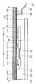
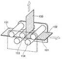
우선, 지지 기판(101) 위에 박리층(102)을 형성한다(도 1의 (A) 참조).First, a
지지 기판(101)으로서는, 적어도 나중의 공정의 가열에 견딜 수 있을 정도의 저항을 갖는 기판을 사용한다. 지지 기판(101)의 예로서는, 유리 기판 및 수지 기판 외에 반도체 기판, 금속 기판, 및 세라믹 기판을 들 수 있다.As the supporting
박리층(102)에는, 텅스텐, 타이타늄, 또는 몰리브데넘 등의 고융점 금속을 사용할 수 있다. 텅스텐을 사용하는 것이 바람직하다.As the
박리층(102)은 예를 들어 스퍼터링법에 의하여 형성할 수 있다. 박리층(102)의 두께는 10nm 이상 200nm 이하, 바람직하게는 20nm 이상 100nm 이하이다.The
<피박리층 및 산화물층의 형성>≪ Formation of peel-off layer and oxide layer >
다음에, 박리층(102) 위에 피박리층(110)을 형성하고, 박리층(102)과 피박리층(110) 사이에 산화물층(111)을 형성한다(도 1의 (B) 참조).Next, a
피박리층(110)은, 산화질화 실리콘을 포함하는 제 1 층(103) 및 질화 실리콘을 포함하는 제 2 층(104)을 이 순서로 포함하는 적층 구조를 갖는다.The layer to be peeled 110 has a laminated structure including a
또한, 본 명세서 등에 있어서, '산화질화 실리콘'은 질소보다 산소를 많이 포함하고, '질화산화 실리콘'은 산소보다 질소를 많이 포함한다.Also, in this specification and the like, 'silicon oxynitride' contains more oxygen than nitrogen and 'silicon nitride oxide' contains more nitrogen than oxygen.
제 1 층(103)은 나중의 가열 공정에서 수소와 질소를 방출할 수 있다. 제 2 층(104)은 나중의 가열 공정에서 수소를 방출하고, 제 1 층(103)으로부터 외부로 질소가 방출되는 것을 억제(즉, 질소 방출을 블로킹)하는 기능을 갖는다.The
제 1 층(103)은, SIMS에 의하여 검출되는 질소 함유량이 5.0×10²⁰분자/cm3 이상 1.0×10²³분자/cm3 이하, 바람직하게는 1.0×10²¹분자/cm3 이상 5.0×10²²분자/cm3 이하인 영역과, 수소 함유량이 1.0×10²⁰분자/cm3 이상 1.0×10²²분자/cm3 이하, 바람직하게는 5.0×10²⁰분자/cm3 이상 5.0×10²¹분자/cm3 이하인 영역을 포함하는 산화질화 실리콘막을 포함하는 것이 바람직하다.The
또한, 제 1 층(103)은, 질량전하비 28에서의 TDS에 의하여 얻어지는 스펙트럼에 있어서, 100℃~450℃의 온도 범위에서 산화질화 실리콘막으로부터 방출되는 질소의 양이, 질소 분자로 환산하였을 때 5×10¹⁷분자/cm3 이상, 바람직하게는 1×10¹⁸분자/cm3 이상이고, 질량전하비 2에서의 TDS에 의하여 얻어지는 스펙트럼에 있어서, 100℃~450℃의 온도 범위에서 산화질화 실리콘막으로부터 방출되는 수소의 양이, 수소 분자로 환산하였을 때 5×10¹⁹분자/cm3 이상, 바람직하게는 1×10²⁰분자/cm3 이상인 산화질화 실리콘막을 포함하는 것이 바람직하다.In the spectrum obtained by the TDS at the
또한, 제 2 층(104)은, 질량전하비 28에서의 TDS에 의하여 얻어지는 스펙트럼에 있어서, 100℃~450℃의 온도 범위에서 질화 실리콘막으로부터 방출되는 질소의 양이, 질소 분자로 환산하였을 때 5×10¹⁹분자/cm3 이하, 바람직하게는 1×10¹⁹분자/cm3 이하이고, 질량전하비 2에서의 TDS에 의하여 얻어지는 스펙트럼에 있어서, 100℃~450℃의 온도 범위에서 질화 실리콘막으로부터 방출되는 수소의 양이, 수소 분자로 환산하였을 때 1×10²⁰분자/cm3 이상, 바람직하게는 5×10²⁰분자/cm3 이상인 질화 실리콘막을 포함하는 것이 바람직하다.When the amount of nitrogen released from the silicon nitride film in the temperature range of 100 DEG C to 450 DEG C in the spectrum obtained by the TDS at the
제 1 층(103)은 스퍼터링법 또는 플라즈마 CVD법 등에 의하여 형성할 수 있다. 특히, 제 1 층(103)에 포함되는 산화질화 실리콘막은, 실레인 가스 및 일산화 이질소 가스를 포함하는 성막 가스를 사용하여 플라즈마 CVD법에 의하여 형성하면, 막에 다량의 수소 및 질소를 포함시킬 수 있어 바람직하다. 또한, 성막 가스에서의 실레인 가스의 비율이 높을수록 나중의 가열 공정에서 막으로부터 방출되는 수소의 양이 증가되어 바람직하다.The
제 2 층(104)은 스퍼터링법 또는 플라즈마 CVD법 등에 의하여 형성할 수 있다. 특히, 제 2 층(104)에 포함되는 질화 실리콘막을 실레인 가스, 질소 가스, 암모니아 가스를 포함하는 성막 가스를 사용하여 플라즈마 CVD법에 의하여 형성하면, 막에 다량의 수소를 함유시킬 수 있다.The
제 1 층(103)의 두께는 방출되는 수소 및 질소의 양의 증가를 위하여 두꺼운 것이 바람직하지만, 생산성을 고려하여 결정되는 것이 바람직하다. 한편, 제 1 층(103)의 두께가 지나치게 얇으면, 방출되는 수소 및 질소의 양이 불충분해진다. 제 1 층(103)의 두께는 200nm 이상 1μm 이하, 바람직하게는 400nm 이상 800nm 이하이다.The thickness of the
제 2 층(104)의 두께는 적어도 질소의 방출을 블로킹할 수 있는 한 특별히 한정되지 않는다. 예를 들어, 50nm 이상 600nm 이하, 바람직하게는 100nm 이상 300nm 이하의 두께인 것이 바람직하다.The thickness of the
박리층(102)의 표면은, 제 1 층(103) 형성 시에 산화되어, 박리층(102)과 제 1 층(103) 사이에 산화물층(111)이 형성된다.The surface of the
산화물층(111)은 박리층(102)에 포함되는 금속의 산화물을 포함한다. 산화물층(111)은 산화 텅스텐을 포함하는 것이 바람직하다.The
산화 텅스텐은 일반적으로 WO(3-x)로 표시되고, 대표적으로는 WO3, W2O5, W4O11, 및 WO2 등 다양한 조성을 가질 수 있는 비화학량적 화합물이다. 산화 타이타늄 TiO(2-x) 및 산화 몰리브데넘 MoO(3-x)도 비화학량적 화합물이다.Tungsten oxide is generally a non-stoichiometric compound represented by WO(3-x) , typically having various compositions such as WO3 , W2 O5 , W4 O11 , and WO2 . Titanium oxide TiO2(2-x) and molybdenum oxide MoO3(3-x) are also non-stoichiometric compounds.
이 단계에서 산화물층(111)은 다량의 산소를 포함하는 것이 바람직하다. 예를 들어, 박리층(102)에 텅스텐을 사용한 경우에는, 산화물층(111)은 그 주성분으로서 WO3을 포함하는 산화 텅스텐층인 것이 바람직하다.At this stage, the
제 1 층(103)을 형성하기 전에, 일산화 이질소 가스를 포함하는 분위기에서 박리층(102)의 표면에 플라즈마 처리를 수행하여, 박리층(102)의 표면에 산화물층(111)을 미리 형성할 수도 있다. 이와 같은 방법을 사용하면, 플라즈마 처리의 조건에 따라 산화물층(111)의 두께를 변화시킬 수 있고, 플라즈마 처리를 수행하지 않는 경우에 비하여 산화물층(111)의 두께를 더 효율적으로 제어할 수 있다.The surface of the
산화물층(111)의 두께는 예를 들어 0.1nm 이상 100nm 이하, 바람직하게는 0.5nm 이상 20nm 이하이다. 또한, 두께가 매우 얇은 산화물층(111)은 단면 이미지에 있어서 관찰할 수 없는 경우가 있다.The thickness of the
<가열 처리><Heat Treatment>
다음에, 가열 처리를 수행하여 산화물층(111)의 성질을 변화시킨다.Next, a heat treatment is performed to change the properties of the
가열 처리에 의하여, 제 1 층(103) 및 제 2 층(104)으로부터 수소가 방출되어 산화물층(111)에 공급된다. 또한, 제 1 층(103)으로부터 질소가 방출되어 산화물층(111)에 공급된다. 이 때, 제 2 층(104)은 질소의 방출을 블로킹하기 때문에, 산화물층(111)에 질소를 효율적으로 공급할 수 있다.Hydrogen is discharged from the
가열 처리는 제 1 층(103)으로부터 질소 및 수소가 방출되는 온도 이상, 지지 기판(101)이 유연해지는 온도 이하에서 수행하면 좋다. 또한, 가열 처리는, 산화물층(111) 내의 수소와 금속 산화물 간의 환원 반응이 일어나는 온도 이상에서 수행하는 것이 바람직하다. 예를 들어, 박리층(102)에 텅스텐을 사용한 경우에는, 가열 온도는 420℃ 이상, 450℃ 이상, 600℃ 이상, 또는 650℃ 이상이다.The heat treatment may be performed at a temperature higher than the temperature at which nitrogen and hydrogen are emitted from the
가열 처리의 온도가 높을수록, 제 1 층(103)으로부터 방출되는 질소의 양과 제 1 층(103) 및 제 2 층(104)으로부터 방출되는 수소의 양이 많아져, 박리성을 향상시킬 수 있다. 그러나, 지지 기판(101)의 내열성 및 생산성을 고려하여 가열 온도를 낮추더라도, 상술한 바와 같이 박리층(102)에 플라즈마 처리를 수행하여 산화물층(111)을 미리 형성함으로써, 높은 박리성을 실현할 수 있다.The higher the temperature of the heat treatment, the greater the amount of nitrogen released from the
가열 처리를 수행하는 분위기는 특별히 한정되지 않고 대기 분위기일 수도 있지만, 질소 분위기 또는 희가스 분위기 등의 불활성 분위기에서 수행하는 것이 바람직하다.The atmosphere for performing the heat treatment is not particularly limited and may be an atmospheric atmosphere, but it is preferably carried out in an inert atmosphere such as a nitrogen atmosphere or a rare gas atmosphere.
가열 처리에 의하여 피박리층(110)으로부터 방출된 수소 및 질소는 제 1 층(103)과 박리층(102) 사이에 트랩된다. 결과적으로, 제 1 산화물층(103)과 박리층(102) 사이의 산화물층(111)에, 수소 농도가 높은 영역과 질소 농도가 높은 영역이 형성된다.The hydrogen and nitrogen discharged from the layer to be peeled 110 by the heat treatment are trapped between the
예를 들어, SIMS에 의하여 측정되는 수소 농도가 제 1 층(103)보다 높은 영역이 산화물층(111)에 형성된다. 또한, SIMS에 의하여 측정되는 질소 농도가 제 1 층(103)보다 높은 영역이 산화물층(111)에 형성된다.For example, a region where the hydrogen concentration measured by SIMS is higher than the
산화물층(111)에 공급된 수소에 의하여 산화물층(111) 내의 금속 산화물이 환원되어, 산소의 비율이 다른 복수의 영역이 산화물층(111) 중에 혼합된다. 예를 들어, 박리층(102)에 텅스텐을 사용한 경우에는, 산화물층(111)의 WO3이 환원되어 WO3보다 산소의 비율이 낮은 산화물(예를 들어 WO2)이 형성되고, 그 결과 산소의 비율이 낮은 산화물과 WO3이 혼합된 상태가 된다. 이러한 금속 산화물의 결정 구조는 산소의 비율에 의존하기 때문에, 산소의 비율이 다른 복수의 영역이 산화물층(111)에 제공되면, 산화물층(111)의 기계적 강도가 저하된다. 그 결과, 산화물층(111)은 내부에서 손상되기 쉬워져, 나중의 박리 공정에서의 박리성을 향상시킬 수 있다.The metal oxide in the
또한, 산화물층(111)에 질소가 공급되기 때문에, 산화물층(111) 내의 금속과 질소를 포함하는 화합물도 생성된다. 예를 들어, 박리층(102)에 텅스텐을 사용한 경우에는, W-N 결합을 갖는 화합물이 산화물층(111)에 생성된다.Further, since nitrogen is supplied to the
가열 처리된 산화물층(111)에 포함되는 W-N 결합을 갖는 화합물은, 예를 들어, 박리 후에 잔존한 산화물층(111)의 일부의 표면에 수행되는 XPS(X-ray photoelectron spectroscopy)를 사용한 분석에 의하여 확인할 수 있다.The compound having a WN bond included in the heat-treated
산화물층(111) 내의 금속과 질소를 포함하는 화합물은, 산화물층(111)의 기계적 강도를 더 저하시킬 수 있어, 박리성을 향상시킬 수 있다.A compound containing a metal and nitrogen in the
가열 처리의 전후에서 산화물층(111)의 단면 형상에 현저한 차이를 볼 수 있다. 이하에서는 가열 처리 전후에서의 산화물층(111)의 단면 형상에 대하여 설명한다.A noticeable difference can be seen in the cross-sectional shape of the
도 2의 (A) 및 (B)는 각각 가열 처리 전후에서의, 도 1의 (B)의 파선으로 둘러싼 영역을 확대한 단면 개략도를 도시한 것이다.Figs. 2A and 2B are schematic cross-sectional views each showing an enlarged view of the region surrounded by the broken line in Fig. 1B before and after the heat treatment.
가열 처리 전에서는, 도 2의 (A)에 도시된 바와 같이 단면에서 박리층(102)과 제 1 층(103) 사이에 산화물층(111)이 관찰된다.Before the heat treatment, as shown in Fig. 2A, an
한편, 가열 처리 후의 박리층(102)과 산화물층(111)의 단면 관찰에서는, 도 2의 (B)에 도시된 바와 같이, 이들의 계면 부근에 박리층(102) 및 산화물층(111)과는 그레이 레벨(gray level)이 다른 영역(112)을 관찰할 수 있다. 그레이 레벨이 다른 영역(112)은 TEM(transmission electron microscope)에 의하여 관찰할 수 있다.On the other hand, in the observation of the
영역(112)은, 박리층(102)과 산화물층(111)이 서로 부분적으로 분리되었을 때 형성된 공동(cavity)일 가능성이 있다. 또는, 영역(112)은, 산화물층(111)에 포함되는 원소를 포함하며 산화물층(111)보다 밀도가 낮은 영역일 가능성도 있다. 또는, 영역(112)은, 박리층(102)과 산화물층(111)과 피박리층(110)의 각각의 구성 요소 중 여러 개를 포함한 층, 또는 산화물층(111)으로부터 방출된 질소, 산소, 또는 수소 등이 기체 상태로 존재하는 영역일 가능성도 있다.The
예를 들어, 피박리층(110)으로서 제 1 층(103)만 또는 제 2 층(104)만을 사용한 경우에는, 가열 처리를 수행하더라도 영역(112)은 형성되지 않는다. 또한, 제 1 층(103)과 제 2 층(104)의 순서를 교대한 경우에도 영역(112)을 관찰할 수 없다. 이는 산화물층(111)으로부터 방출된 질소, 수소, 또는 산소 등의 원소가 영역(112)의 형성에 관여하는 것을 가리킨다.For example, when only the
가열 처리를 수행하는 경우와 가열 처리를 수행하지 않는 경우, 즉 영역(112)의 존재 여부에 따라, 나중의 박리 공정에서 박리에 요구되는 외력이 현저히 달라진다. 가열 처리에 의하여 영역(112)이 형성되었을 때 더 약한 힘으로 박리를 수행할 수 있다. 이는 영역(112)이 박리성의 향상에 크게 기여하는 것을 가리킨다.In the case of performing the heat treatment and in the case of not performing the heat treatment, that is, depending on whether or not the
예를 들어, 영역(112)이 공동이거나 가스로 충전된 경우, 산화물층(111)과 박리층(102)의 접촉 면적이 축소되어 접착성이 낮아지므로 박리성이 향상될 것으로 생각된다. 또한, 영역(112)이 박리층(102)과 산화물층(111)과는 다른 조성을 갖거나 또는 영역(112)의 밀도가 낮은 경우에는, 산화물층(111)과 박리층(102) 사이의 접착성과 영역(112)과 박리층(102) 사이의 접착성의 차이에 의하여 박리성이 향상될 것으로 생각된다.For example, when the
<접착><Adhesion>
다음에, 지지 기판(101)과 기판(121)을 접착층(122)에 의하여 서로 접착시킨다(도 1의 (C) 참조).Next, the
기판(121)으로서는 가요성 기판을 사용하는 것이 바람직하다. 예를 들어, 폴리에틸렌테레프탈레이트(PET) 또는 폴리에틸렌나프탈레이트(PEN) 등의 수지 외에, 가요성을 가질 정도로 얇은 금속 기판 또는 유리 기판을 사용할 수 있다. 금속, 유리, 및 수지 중 2개 이상이 적층된 복합 재료를 사용할 수도 있다.As the
기판(121)은 반드시 가요성을 가질 필요는 없고, 이 경우에는 지지 기판(101)과 같은 재료를 기판(121)에 사용할 수 있다. 트랜지스터 등의 반도체 소자, 유기 일렉트로루미네선스(EL) 소자 등의 발광 소자, 또는 액정 소자 등의 광학 소자가 형성된 기판을 기판(121)으로서 사용할 수도 있다.The
수지가 피접착면들을 고착시킬 수 있는 한, 열 경화 수지 또는 자외선 경화 수지를 접착층(122)에 사용할 수 있다. 예를 들어, 아크릴 수지, 우레탄 수지, 에폭시 수지, 또는 실록산 결합을 갖는 수지를 사용할 수 있다. 나중에 기판(121)을 제거하는 경우에는, 수용성(水溶性) 수지 또는 유기 용매에 가용(可溶)인 수지 등을 사용할 수 있다.A thermosetting resin or an ultraviolet curing resin may be used for the
<박리><Peeling>
다음에, 산화물층(111)에서 피박리층(110)으로부터 박리층(102)을 박리한다(도 1의 (D) 참조).Next, the
박리를 위하여, 예를 들어 지지 기판(101) 또는 기판(121)을 흡인 스테이지에 고정하고, 박리층(102)과 피박리층(110) 사이에 박리 기점을 형성한다. 박리 기점은, 예를 들어 층들 사이에 칼 등의 예리한 기구를 넣음으로써 형성하여도 좋다. 또는, 박리 기점은, 박리층(102)의 일부를 레이저 광으로 조사하여 용해시킴으로써 형성하여도 좋다. 또는, 박리 기점은, 액체(예를 들어 알코올, 물, 또는 이산화 탄소를 포함한 물)를 예를 들어 박리층(102) 또는 피박리층(110)의 단부에 적하하여, 모세관 현상(capillary action)을 사용하여 상기 액체를 박리층(102)과 피박리층(110)의 경계에 침투시킴으로써 형성하여도 좋다.For example, the supporting
그리고, 박리 기점이 형성된 부분에 접착면에 실질적으로 수직인 방향으로 물리적인 힘을 약하게 가함으로써, 피박리층(110)에 대한 대미지 없이 박리를 일으킬 수 있다. 이 때, 지지 기판(101) 또는 기판(121)에 테이프 등을 부착시키고 이 테이프를 상술한 방향으로 당기거나, 또는 갈고리 형상 부재로 지지 기판(101) 또는 기판(121)의 단부를 당김으로써 박리를 일으켜도 좋다. 또는, 지지 기판(101) 또는 기판(121)의 이면에 부착된 접착 부재나 진공 흡인이 가능한 부재를 당김으로써 박리를 일으켜도 좋다.By weakly applying a physical force to the portion where the peeling starting point is formed in a direction substantially perpendicular to the bonding surface, peeling can be caused without damaging the layer to be peeled 110. At this time, by attaching a tape or the like to the
여기서, 물 또는 수용액 등 물을 포함한 액체를 박리 계면에 첨가하여 이 액체를 상기 박리 계면에 침투시켜 박리를 수행함으로써, 박리성을 향상시킬 수 있다. 액체를 첨가한 경우에 박리성이 향상되는 이유에 대해서는 다른 실시형태에서 자세히 설명한다.Here, a liquid containing water such as water or an aqueous solution is added to the peeling interface, and this liquid is permeated into the peeling interface to perform peeling, whereby the peeling property can be improved. The reason why the peelability is improved when the liquid is added will be described in detail in another embodiment.
박리는, 산화물층(111) 내부, 및 산화물층(111)과 박리층(102)의 계면에서 주로 생긴다. 따라서, 도 1의 (D)에 도시된 바와 같이, 박리 후에 산화물층(111)의 일부는 박리층(102) 및 제 1 층(103)의 각 표면에 부착되는 경우가 있다. 또한, 박리층(102)의 표면 위의 산화물층(111)의 두께는 제 1 층(103)의 표면 위의 산화물층(111)의 두께와는 달라도 좋다. 산화물층(111)과 박리층(102)의 계면에서 박리가 생기기 쉽기 때문에, 제 1 층(103) 측의 산화물층(111)의 두께는 박리층(102) 측의 산화물층(111)의 두께보다 두꺼운 경우가 많다.The peeling mainly occurs at the interface between the
상술한 방법에 의하여, 박리층(102)과 피박리층(110)을 수율 좋게 서로 분리할 수 있다.By the above-described method, the
<접착><Adhesion>
그 후, 도 1의 (E)에 도시된 바와 같이, 피박리층(110)의 박리된 표면에 접착층(132)을 개재(介在)하여 기판(131)을 접착시켜도 좋다. 접착층(132) 및 기판(131)에 대해서는 접착층(122) 및 기판(121)의 기재를 각각 참조할 수 있다.Thereafter, the
기판(121) 및 기판(131)으로서 가요성 기판을 사용함으로써 플렉시블 적층체를 형성할 수 있다.By using a flexible substrate as the
[적용예][Application example]
상기 제작 방법의 예에서 설명한 박리 방법은 다양한 플렉시블 디바이스에 적용할 수 있다.The peeling method described in the example of the production method can be applied to various flexible devices.
예를 들어, 트랜지스터를 포함하는 플렉시블 디바이스에 상기 박리 방법을 사용하는 경우에는, 피박리층(110)을 형성한 후에 트랜지스터를 형성하여도 좋다.For example, when the above-described separation method is used for a flexible device including a transistor, a transistor may be formed after the layer to be peeled 110 is formed.
예를 들어, 보텀 게이트 트랜지스터를 제작하는 경우, 피박리층(110) 위에, 게이트 전극, 게이트 절연층, 반도체층, 소스 전극 및 드레인 전극을 이 순서로 형성한다. 그 후, 기판(121)을 접착시키는 공정, 박리 공정, 기판(131)을 접착시키는 공정을 수행한다. 이와 같이 함으로써, 트랜지스터를 포함하는 플렉시블 디바이스를 제작할 수 있다.For example, when a bottom gate transistor is fabricated, a gate electrode, a gate insulating layer, a semiconductor layer, a source electrode, and a drain electrode are formed in this order on the layer to be peeled 110. Thereafter, a step of bonding the
또한, 스태거형 트랜지스터 또는 역 스태거형 트랜지스터 등을 사용하여도 좋다. 또한, 톱 게이트 트랜지스터 또는 보텀 게이트 트랜지스터를 사용하여도 좋다. 또한 채널 에치(channel-etched)형 트랜지스터 또는 채널 보호형 트랜지스터를 사용하여도 좋다. 채널 보호형 트랜지스터의 경우, 채널 영역 위에만 채널 보호막을 제공하여도 좋다. 또는, 소스 전극 및 드레인 전극과 반도체층이 접하는 부분에만 개구를 형성하고, 그 개구 이외의 부분에 채널 보호막을 제공하여도 좋다.In addition, a staggered transistor or a reverse staggered transistor may be used. A top gate transistor or a bottom gate transistor may also be used. A channel-etched transistor or a channel-protected transistor may also be used. In the case of a channel-protected transistor, a channel protective film may be provided only over the channel region. Alternatively, an opening may be formed only in a portion where the source electrode and the drain electrode are in contact with the semiconductor layer, and a channel protective film may be provided in a portion other than the opening.
트랜지스터의 채널이 형성되는 반도체층에 적용할 수 있는 반도체로서 예를 들어 실리콘이나 저마늄 등의 반도체 재료, 화합물 반도체 재료, 유기 반도체 재료, 또는 산화물 반도체 재료를 사용하여도 좋다.A semiconductor material such as silicon or germanium, a compound semiconductor material, an organic semiconductor material, or an oxide semiconductor material may be used as the semiconductor applicable to the semiconductor layer in which the channel of the transistor is formed.
또한, 트랜지스터에 사용하는 반도체의 결정성에 대한 제한은 특별히 없고, 비정질 반도체, 또는 결정성을 갖는 반도체(미결정 반도체, 다결정 반도체, 단결정 반도체, 또는 결정 영역을 부분적으로 포함한 반도체)를 사용하여도 좋다. 결정성을 갖는 반도체를 사용하면, 트랜지스터 특성의 열화를 저감할 수 있어 바람직하다.There is no particular limitation on the crystallinity of the semiconductor used for the transistor, and an amorphous semiconductor or a semiconductor having crystallinity (a microcrystalline semiconductor, a polycrystalline semiconductor, a single crystal semiconductor, or a semiconductor partially including a crystal region) may be used. Use of a semiconductor having crystallinity is preferable because deterioration of transistor characteristics can be reduced.
예를 들어, 상기 반도체로서 실리콘을 사용하는 경우, 비정질 실리콘, 미결정 실리콘, 다결정 실리콘, 또는 단결정 실리콘 등을 사용할 수 있다.For example, when silicon is used as the semiconductor, amorphous silicon, microcrystalline silicon, polycrystalline silicon, monocrystalline silicon, or the like can be used.
또한, 상기 반도체로서 산화물 반도체를 사용하는 경우, 인듐, 갈륨, 및 아연 중 적어도 하나를 포함하는 산화물 반도체를 사용하는 것이 바람직하다. 대표적으로는 In-Ga-Zn계 금속 산화물을 들 수 있다. 실리콘보다 밴드 갭이 넓고 캐리어 밀도가 낮은 산화물 반도체를 사용하면, 오프 상태에서의 누설 전류를 저감할 수 있어 바람직하다.When an oxide semiconductor is used as the semiconductor, it is preferable to use an oxide semiconductor containing at least one of indium, gallium, and zinc. Typically, the In-Ga-Zn-based metal oxide may be mentioned. The use of an oxide semiconductor having a wider bandgap than silicon and a lower carrier density is preferable because the leakage current in the OFF state can be reduced.
본 발명의 일 형태에 따른 박리 방법에서는, 지지 기판 위에 소자를 형성한 후에 박리를 수행하여 가요성을 얻을 수 있기 때문에, 소자 형성 공정에서의 온도에 거의 제한이 없다. 그러므로, 고온 프로세스를 거쳐 제작되며 신뢰성이 매우 높은 반도체 소자를, 내열성이 떨어지는 가요성 기판 위에 높은 수율로 제작할 수 있다.In the peeling method according to an embodiment of the present invention, since the peeling can be performed by forming the element on the supporting substrate to obtain flexibility, there is almost no limitation on the temperature in the element forming step. Therefore, a highly reliable semiconductor device manufactured through a high-temperature process can be manufactured with a high yield on a flexible substrate having low heat resistance.
발광성 유기 화합물을 포함한 층이 한 쌍의 전극 사이에 개재된 발광 소자를 피박리층(110) 위에 형성함으로써, 플렉시블 발광 장치를 제작할 수 있다. 예를 들어, 발광 소자를 포함하는 플렉시블 조명 장치(또는 광원)를 제작할 수 있고, 또는 트랜지스터와, 발광 소자 및 액정 소자 등의 표시 소자를 포함하는 복수의 화소를 피박리층(110) 위에 형성함으로써, 화상 표시 장치를 제작하여도 좋다. 플렉시블 화상 표시 장치의 예에 대해서는 다른 실시형태에서 설명한다.A flexible light emitting device can be manufactured by forming a light emitting element in which a layer containing a light emitting organic compound is sandwiched between a pair of electrodes on a layer to be peeled 110. [ For example, a flexible lighting device (or a light source) including a light emitting element can be manufactured, or a plurality of pixels including a transistor, a light emitting element, and a liquid crystal element including a display element can be formed on the layer to be peeled 110 , An image display apparatus may be manufactured. An example of a flexible image display device will be described in another embodiment.
또한, 본 실시형태는 본 명세서에서 설명하는 다른 실시형태 및 실시예 중 어느 것과 적절히 조합할 수 있다.The present embodiment can be appropriately combined with any of the other embodiments and the embodiments described in this specification.
(실시형태 2)(Embodiment 2)
본 실시형태에서는, 본 발명의 일 형태에 따른 박리 방법에 의하여 제작할 수 있는 플렉시블 디바이스에 대하여 도면을 참조하여 설명한다. 플렉시블 디바이스의 예로서, 유기 EL 소자를 포함하는 화상 표시 장치(이하에서 표시 장치) 및 조명 장치 등의 발광 장치에 대하여 설명한다.In the present embodiment, a flexible device that can be manufactured by the exfoliation method according to an embodiment of the present invention will be described with reference to the drawings. As an example of a flexible device, a light emitting device such as an image display device (hereinafter referred to as a display device) and an illumination device including an organic EL device will be described.
또한, 본 명세서에서의 발광 장치는 화상 표시 장치 또는 광원(조명 장치를 포함함)을 말한다. 또한, 발광 장치는, FPC(Flexible Printed Circuit) 또는 TCP(Tape Carrier Package) 등의 커넥터가 발광 장치에 부착된 모듈, TCP 끝에 인쇄 배선판이 제공된 모듈, 발광 소자가 형성된 기판에 COG(Chip On Glass)법에 의하여 직접 탑재된 IC(Integrated Circuit)를 갖는 모듈, 터치 센서가 탑재된 모듈 중 어느 것을 그 범주에 포함할 수 있다.The light emitting device in this specification refers to an image display device or a light source (including a lighting device). The light emitting device may be a module in which a connector such as an FPC (Flexible Printed Circuit) or a TCP (Tape Carrier Package) is attached to a light emitting device, a module in which a printed wiring board is provided at a TCP end, a chip on glass (COG) A module having an integrated circuit (IC) directly mounted by a method, or a module equipped with a touch sensor can be included in the category.
본 명세서 등에서 '반도체 장치'는 반도체 특성을 이용함으로써 동작할 수 있는 모든 장치를 뜻한다. 트랜지스터, 반도체 회로, 기억 장치, 촬상 장치, 전기 광학 장치, 발전 장치(예를 들어, 박막 태양 전지 및 유기 박막 태양 전지), 및 전자 기기 등은 반도체 장치에 포함되거나 반도체 장치를 포함하여도 좋다.As used herein, the term "semiconductor device" refers to any device that can operate by utilizing semiconductor properties. A transistor, a semiconductor circuit, a memory device, an imaging device, an electro-optical device, a power generation device (for example, a thin film solar cell and an organic thin film solar cell), and an electronic device may be included in the semiconductor device or may include a semiconductor device.
따라서, 이하에서 설명하는 발광 장치들 중, 반도체 특성을 갖는 소자(예를 들어 트랜지스터)를 포함하는 발광 장치도 반도체 장치의 일 형태이다. 즉, 이러한 발광 장치는 발광 소자 및 반도체 장치를 포함한다.Therefore, among the light-emitting devices described below, a light-emitting device including an element (for example, a transistor) having semiconductor characteristics is also a form of a semiconductor device. That is, such a light emitting device includes a light emitting element and a semiconductor device.
[표시 장치의 구성예 1][Configuration Example 1 of Display Apparatus]
도 3의 (A)는 톱 이미션 구조를 갖는 표시 장치(200)의 상면 개략도이다.3 (A) is a schematic top view of a
표시 장치(200)는 가요성 기판(254) 상면에 표시부(201), 주사선 구동 회로(202), 및 신호선 구동 회로(203)를 포함한다. 또한, 표시 장치(200)는 표시부(201)를 덮는 밀봉층(252) 및 밀봉층(252) 위의 가요성 기판(253)을 포함한다. 표시 장치(200)에서, 가요성 기판(254) 위에, 주사선 구동 회로(202) 및 신호선 구동 회로(203)에 전기적으로 접속되는 외부 접속 단자(204)가 제공된다. 외부 접속 단자(204)에 전기적으로 접속되는 FPC(205)를 통하여, 주사선 구동 회로(202) 및 신호선 구동 회로(203) 등을 구동하기 위한 전원 전위 및 구동 신호 등의 신호를 외부로부터 입력할 수 있다.The
도 3의 (B)는, 도 3의 (A)에 도시된 외부 접속 단자(204), 주사선 구동 회로(202), 및 표시부(201)를 포함하는 영역을 자른 선 A-B 및 C-D를 따른 단면 개략도이다.3B is a schematic cross-sectional view along the cut lines AB and CD of the region including the
표시 장치(200)에서, 제 1 층(103) 및 제 2 층(104)을 포함한 피박리층(110)이 접착층(132)을 개재하여 가요성 기판(254) 위에 제공된다. 또한, 발광 소자(240), 주사선 구동 회로(202)(및 신호선 구동 회로(203)), 및 외부 접속 단자(204)가 제 2 층(104) 위에 제공된다.In the
외부 접속 단자(204)는, 표시 장치(200)의 트랜지스터 또는 발광 소자에 포함되는 도전층과 같은 재료를 사용하여 형성된다. 본 구성예에서는, 트랜지스터의 게이트 전극을 형성하는 도전층과 같은 재료를 사용하여 형성된 층과, 트랜지스터의 소스 전극 및 드레인 전극을 형성하는 도전층과 같은 재료를 사용하여 형성된 층이 적층된다. 외부 접속 단자(204)는 복수의 층을 포함하는 이러한 적층을 포함함으로써, 기계적 강도가 높아지고 전기 저항이 저감될 수 있어 바람직하다. 커넥터(206)는 외부 접속 단자(204)와 접하여 제공된다. FPC(205)는 커넥터(206)를 통하여 외부 접속 단자(204)에 전기적으로 접속된다. 커넥터(206)는, 열 경화성 수지에 도전성 입자가 혼합되며 열 압착에 의하여 이방성의 도전성을 나타내는 페이스트상의 재료, 또는 열 경화성 수지의 내부에 도전성 입자가 포함되며 열 압착에 의하여 이방성의 도전성을 나타내는 시트상 재료를 사용하여 형성할 수 있다. 도전성 입자의 예로서는, 금속으로 피복된 니켈 입자, 및 금속으로 피폭된 수지를 들 수 있다.The
도 3의 (B)에서, 주사선 구동 회로(202)는 예를 들어 n채널형 트랜지스터(211)와 n채널형 트랜지스터(212)가 조합된 회로를 부분적으로 포함한다. 또한, 주사선 구동 회로(202)는, n채널형 트랜지스터들이 조합된 회로에 한정되지 않고, n채널형 트랜지스터와 p채널형 트랜지스터가 조합된 CMOS 회로나 p채널형 트랜지스터가 조합된 회로 등 다양한 회로를 포함하여도 좋다. 또한, 신호선 구동 회로(203)에 대해서도 마찬가지이다. 본 구성예에서는, 표시부(201)가 형성된 절연 표면 위에 주사선 구동 회로(202) 및 신호선 구동 회로(203)가 형성된 드라이버 일체형 구조를 설명하였지만, 예를 들어, 주사선 구동 회로(202) 및 신호선 구동 회로(203) 중 하나 또는 양쪽으로서 사용되는 구동 회로 IC를 COG법에 의하여 탑재하여도 좋고, 또는 COF(Chip On Film)법에 의하여 구동 회로 IC가 탑재된 가요성 기판(FPC)을 탑재하여도 좋다.In Fig. 3B, the scanning
도 3의 (B)는, 표시부(201)의 일례로서 하나의 화소의 단면 구조를 도시한 것이다. 화소는 스위칭 트랜지스터(213), 전류 제어 트랜지스터(214), 및 전류 제어 트랜지스터(214)의 전극(소스 전극 또는 드레인 전극)에 전기적으로 접속된 제 1 전극(233)을 포함한다. 제 1 전극(233)의 단부를 덮도록 절연층(219)이 제공된다.FIG. 3B shows a cross-sectional structure of one pixel as an example of the
발광 소자(240)는, 제 1 전극(233), EL층(235), 및 제 2 전극(237)이 절연층(217) 위에 순차적으로 적층된 적층 구조를 갖는다. 본 구성예에서 설명하는 표시 장치(200)는 톱 이미션 표시 장치이기 때문에, 제 2 전극(237)에는 투광성 재료를 사용한다. 제 1 전극(233)에는 반사성 재료를 사용하는 것이 바람직하다. EL층(235)은 적어도 발광성 유기 화합물을 포함한다. EL층(235)을 개재한 제 1 전극(233)과 제 2 전극(237) 사이에 전압이 인가되어 EL층(235)에 전류가 흐름으로써 발광 소자(240)는 발광할 수 있다.The
제 1 층(243) 및 제 2 층(244)을 포함한 피박리층(245)은, 접착층(242)을 개재하여, 기판(254)과 대향하는 가요성 기판(253) 표면 측에 제공된다. 또한, 발광 소자(240)와 중첩되는 제 2 층(244) 부분에는 컬러 필터(221)가 제공되고, 절연층(219)과 중첩되는 위치에는 블랙 매트릭스(222)가 제공된다. 제 1 층(243) 및 제 2 층(244)은 제 1 층(103) 및 제 2 층(104)과 같은 재료를 사용하여 형성한다. 또한, 기판(254)과 대향하지 않는 기판(253) 표면 위에 투명 도전막을 형성하여 터치 센서를 형성하여도 좋다.The
제 2 층(104) 및 제 2 층(244)은 기판(254) 및 기판(253)에 포함되는 불순물의 확산을 억제하는 기능을 각각 갖는다. 트랜지스터의 반도체층에 접하는 절연층(216) 및 절연층(218)은 반도체층에 대한 불순물 확산을 억제하는 것이 바람직하다. 이들 절연층은 예를 들어, 실리콘 등의 반도체나 알루미늄 등의 금속의 산화물 또는 질화물을 사용하여 형성할 수 있다. 또는, 이러한 무기 절연 재료를 포함하는 적층, 또는 이러한 무기 절연 재료 및 유기 절연 재료를 포함하는 적층을 사용하여도 좋다.The
무기 절연 재료로서는, 예를 들어, 질화 알루미늄, 산화 알루미늄, 질화산화 알루미늄, 산화질화 알루미늄, 산화 마그네슘, 산화 갈륨, 질화 실리콘, 산화 실리콘, 질화산화 실리콘, 산화질화 실리콘, 산화 저마늄, 산화 지르코늄, 산화 란타넘, 산화 네오디뮴, 산화 탄탈럼에서 선택되는 하나 이상의 재료의 단층 또는 적층을 들 수 있다. 본 명세서에서는, 질화산화물은 산소보다 질소의 양이 많은 재료를 가리키고, 산화질화물은 질소보다 산소의 양이 많은 재료를 가리킨다. 원소 함유량은 예를 들어 RBS에 의하여 측정할 수 있다.The inorganic insulating material includes, for example, aluminum nitride, aluminum oxide, aluminum nitride, aluminum oxynitride, magnesium oxide, gallium oxide, silicon nitride, silicon oxide, silicon nitride oxide, silicon oxynitride, A lanthanum oxide, a neodymium oxide, and a tantalum oxide. In this specification, a nitride oxide indicates a material having a larger amount of nitrogen than oxygen, and an oxynitride indicates a material having a larger amount of oxygen than nitrogen. The elemental content can be measured, for example, by RBS.
무기 절연 재료로서 하프늄 실리케이트(HfSiOx), 질소가 첨가된 하프늄 실리케이트(HfSixOyNz), 질소가 첨가된 하프늄 알루미네이트(HfAlxOyNz), 산화 하프늄, 또는 산화 이트륨 등의 high-k 재료를 사용하여도 좋다.(HfSix Oy Nz ) doped with nitrogen, hafnium aluminate (HfAlx Oy Nz ) doped with nitrogen, hafnium silicate (HfSiOx ) doped with nitrogen, hafnium silicate high-k materials may be used.
피박리층(110)은, 실시형태 1에서 설명한 박리 방법에 의하여 박리를 수행함으로써 형성할 수 있다. 피박리층(110) 위에 트랜지스터 및 발광 소자(240)를 형성하고, 박리를 수행한 후에, 접착층(132)을 개재하여 피박리층(110) 이면에 기판(254)을 접착시킴으로써, 도 3의 (B)에 도시된 구조를 얻을 수 있다. 피박리층(245)도 마찬가지로 실시형태 1에서 설명한 박리 방법에 의하여 박리를 수행함으로써 형성할 수 있다. 피박리층(245) 위에 컬러 필터(221) 및 블랙 매트릭스(222)를 형성하고, 박리를 수행한 후에, 접착층(242)을 개재하여 피박리층(245) 이면에 기판(253)을 접착시킴으로써, 도 3의 (B)에 도시된 구조를 얻을 수 있다.The layer to be peeled 110 can be formed by carrying out peeling by the peeling method described in
도 3의 (B)에 도시된 바와 같이, 제 1 층(103)과 접착층(132) 사이에 산화물층(111)을 제공하거나, 또는 제 1 층(243)과 접착층(242) 사이에 산화물층(241)을 제공하여도 좋다. 산화물층(111) 및 산화물층(241)은 매우 얇고 투광성을 갖기 때문에, 발광 소자(240)로부터 사출되는 광이 추출되는 측에 제공되더라도 발광 효율을 저하시키는 일이 거의 없다.An
트랜지스터 등이 제공된 피박리층(110) 및 컬러 필터(221) 등이 제공된 피박리층(245)을 각각 지지 기판이 제공된 상태로 밀봉층(252)에 의하여 서로 접착시키고, 접착 후에 각 지지 기판으로부터 피박리층(110, 245)을 박리하는 것이 바람직하다. 특히, 고정세(高精細)의 표시부(201)를 포함하는 표시 장치와 같이 컬러 필터(221)와 화소가 높은 정밀도로 배치되는 경우, 유리 기판 등의 지지 기판에 고정된 상태로 피박리층을 접착시킴으로써, 컬러 필터(221)와 화소를 높은 정밀도로 배치할 수 있다. 상술한 방법에 의하여 고정세의 플렉시블 표시 장치를 제작할 수 있다.A layer to be peeled 110 provided with a transistor or the like and a layer to be peeled 245 provided with a
또한, 도 3의 (A) 및 (B)는 발광 소자가 표시 소자로서 사용되는 경우를 도시한 것이지만, 본 발명의 일 형태는 이에 한정되지 않는다. 표시 소자로서 액정 소자 또는 전기 영동 소자(전자 종이) 등을 사용할 수 있다. 전기 영동 소자는 백 라이트를 필요로 하지 않기 때문에, 플렉시블 표시 장치의 일 형태로서 바람직하다.3 (A) and 3 (B) show a case where a light emitting element is used as a display element, but one embodiment of the present invention is not limited to this. As a display element, a liquid crystal element or an electrophoretic element (electronic paper) or the like can be used. Since the electrophoretic element does not require a backlight, it is preferable as a form of a flexible display device.
[표시 장치의 구성예 2][Configuration Example 2 of Display Apparatus]
본 구성예에서는, 보텀 이미션 구조를 갖는 표시 장치에 대하여 설명한다. 또한, 구성예 1과 같은 부분은 여기서는 설명하지 않는다.In this configuration example, a display device having a bottom emission structure will be described. The same portions as in the configuration example 1 are not described here.
도 4는 본 구성예에서 설명하는 표시 장치(250)의 단면 개략도이다.Fig. 4 is a schematic cross-sectional view of the
표시 장치(250)는 구성예 1에서 설명한 표시 장치(200)와는 이하의 점에서 주로 다르다. 표시 장치(250)에서는, 기판(254)과 발광 소자(240) 사이에 컬러 필터가 제공된다. 또한, 가요성 기판(253)은 밀봉층(252)과 직접 접하고, 표시 장치(200)에 제공된 피박리층(245) 및 접착층(242) 등은 제공되지 않는다.The
발광 소자(240)에서, 제 1 전극(233)에는 투광성 재료를 사용하고, 제 2 전극(237)에는 반사성 재료를 사용한다. 따라서, EL층(235)으로부터의 발광은 기판(254)을 투과한다.In the
또한, 트랜지스터를 덮는 절연층(218) 위의, 발광 소자(240)와 중첩되는 위치에 컬러 필터(221)가 제공된다. 절연층(217)은 컬러 필터(221)를 덮도록 제공된다.Further, a
기판(253)으로서는, 기판(253) 외부로부터의 물 등의 불순물을 투과시키지 않는 재료를 사용하는 것이 바람직하다. 또는, 밀봉층(252)과 접하는 기판(253) 표면에, 불순물 등의 확산을 억제하는 기능을 가지며 절연 재료로 형성되는 막이 제공되는 것이 바람직하다. 이러한 재료로서, 제 2 층(104, 244)에 사용할 수 있는 무기 절연 재료를 사용할 수 있다.As the
[재료 및 형성 방법][Materials and forming method]
상술한 각 구성 요소에 사용할 수 있는 재료 및 형성 방법에 대하여 이하에서 설명한다.Materials and forming methods that can be used for each of the above-described components will be described below.
<가요성 기판>≪ Flexible substrate &
가요성 기판의 재료로서는, 유기 수지, 또는 가요성을 가질 정도로 얇은 유리 기판 등을 사용할 수 있다.As the material of the flexible substrate, an organic resin or a glass substrate thin enough to have flexibility can be used.
이러한 재료의 예로서는, 폴리에틸렌테레프탈레이트(PET)와 폴리에틸렌나프탈레이트(PEN) 등의 폴리에스터 수지, 폴리아크릴로나이트릴 수지, 폴리이미드 수지, 폴리메틸메타크릴레이트 수지, 폴리카보네이트(PC) 수지, 폴리에터설폰(PES) 수지, 폴리아마이드 수지, 사이클로올레핀 수지, 폴리스타이렌 수지, 폴리아마이드이미드 수지, 및 폴리염화바이닐 수지를 들 수 있다. 특히, 열팽창 계수가 낮은(예를 들어 열팽창 계수가 30×10-6/K 이하인) 재료가 바람직하고, 폴리아마이드이미드 수지, 폴리이미드 수지, 또는 PET를 사용할 수 있다. 또한, 섬유체에 수지가 함침(含浸)된 기판(프리프레그라고도 함), 또는 무기 필러(filler)를 유기 수지와 혼합하여 열팽창 계수를 낮춘 기판을 사용할 수도 있다.Examples of such materials include polyester resins such as polyethylene terephthalate (PET) and polyethylene naphthalate (PEN), polyacrylonitrile resins, polyimide resins, polymethylmethacrylate resins, polycarbonate (PC) (PES) resin, a polyamide resin, a cycloolefin resin, a polystyrene resin, a polyamideimide resin, and a polyvinyl chloride resin. Particularly, a material having a low thermal expansion coefficient (for example, a thermal expansion coefficient of 30 x 10 <-6 > / K or less) is preferable and a polyamideimide resin, a polyimide resin, or PET can be used. Alternatively, a substrate (impregnated with a resin) impregnated with a resin (also referred to as a prepreg) or a substrate having an inorganic filler mixed with an organic resin and having a lower thermal expansion coefficient may be used.
상술한 재료 중에 섬유체가 포함되어 있는 경우에는, 섬유체로서 유기 화합물 또는 무기 화합물의 고강도 섬유를 사용한다. 고강도 섬유는, 구체적으로 인장 탄성률(tensile modulus of elasticity) 또는 영률(Young's modulus)이 높은 섬유이다. 대표적인 예로서는 폴리바이닐알코올계 섬유, 폴리에스터계 섬유, 폴리아마이드계 섬유, 폴리에틸렌계 섬유, 아라미드계 섬유, 폴리파라페닐렌벤조비스옥사졸 섬유, 유리 섬유, 및 탄소 섬유를 들 수 있다. 유리 섬유의 일례로서는 E유리, S유리, D유리, 또는 Q유리 등을 사용한 유리 섬유를 들 수 있다. 이들 섬유는, 직포 또는 부직포의 상태로 사용하고, 이 섬유체에 수지가 함침되고 수지가 경화된 구조물을 가요성 기판으로서 사용하여도 좋다. 가요성 기판으로서 섬유체와 수지를 포함하는 구조물을 사용하면 휨이나 국소적 가압으로 인한 파손에 대한 신뢰성을 높일 수 있어 바람직하다.When the above-mentioned material contains a fibrous substance, high-strength fibers of an organic compound or an inorganic compound are used as the fibrous substance. The high-strength fiber is specifically a fiber having a high tensile modulus of elasticity or Young's modulus. Representative examples include polyvinyl alcohol-based fibers, polyester-based fibers, polyamide-based fibers, polyethylene-based fibers, aramid-based fibers, polyparaphenylenebenzobisoxazole fibers, glass fibers and carbon fibers. Examples of the glass fiber include glass fiber using E glass, S glass, D glass, Q glass, or the like. These fibers may be used in the form of a woven fabric or a nonwoven fabric, and a structure in which a resin is impregnated into the fibrous body and the resin is cured may be used as a flexible substrate. Use of a structure including a fibrous body and a resin as the flexible substrate is preferable because reliability against breakage due to warping or local pressurization can be enhanced.
발광 소자(240)로부터 사출되는 광을 투과시키는 가요성 기판에는, EL층(235)으로부터 사출되는 광을 투과시킬 수 있는 재료를 사용한다. 광을 추출하는 측에 제공하는 재료의 광 추출 효율을 향상시키기 위하여, 가요성 및 투광성의 재료의 굴절률이 높은 것이 바람직하다. 예를 들어, 유기 수지에 굴절률이 높은 무기 필러를 분산시켜 얻어진 기판은, 상기 유기 수지만으로 형성된 기판보다 높은 굴절률을 가질 수 있다. 특히, 입경 40nm 이하의 작은 무기 필러를 사용하면, 광학적인 투명성을 유지할 수 있어 바람직하다.A material capable of transmitting light emitted from the
광을 투과시키는 측과 반대 측에 제공되는 기판은 투광성을 가질 필요가 없기 때문에, 상술한 기판 외에도 금속 기판 등을 사용할 수 있다. 가요성 및 굽힘성(bendability)을 얻기 위해서는, 금속 기판의 두께는 바람직하게는 10μm 이상 200μm 이하, 더 바람직하게는 20μm 이상 50μm 이하이다. 금속 기판의 재료에 대하여 특별한 제한은 없지만, 예를 들어, 알루미늄, 구리, 니켈, 알루미늄 합금이나 스테인리스 강 등의 금속의 합금을 사용하는 것이 바람직하다. 광을 투과시키지 않는 측에 제공되는 가요성 기판으로서는 금속 또는 합금 재료를 포함하는 도전성 기판을 사용하면, 발광 소자(240)로부터 발생되는 열에 대한 방열성을 향상시킬 수 있어 바람직하다.The substrate provided on the side opposite to the side through which the light is transmitted need not have transparency, so that a metal substrate or the like other than the above-described substrate can be used. In order to obtain flexibility and bendability, the thickness of the metal substrate is preferably not less than 10 μm and not more than 200 μm, more preferably not less than 20 μm and not more than 50 μm. There is no particular limitation on the material of the metal substrate. For example, it is preferable to use an alloy of a metal such as aluminum, copper, nickel, aluminum alloy, or stainless steel. As the flexible substrate provided on the side where light is not transmitted, the use of a conductive substrate including a metal or alloy material is preferable because heat dissipation to heat generated from the
도전성 기판을 사용하는 경우에는, 이 기판의 표면을 산화시키거나, 또는 기판의 표면에 절연막을 형성하는 등의 절연 처리를 수행한 기판을 사용하는 것이 바람직하다. 예를 들어, 전착법, 스핀 코팅법이나 딥법(dip method) 등의 도포법, 스크린 인쇄법 등의 인쇄법, 또는 증착법이나 스퍼터링법 등의 퇴적법 등의 방법에 의하여 도전성 기판 표면에 절연막을 형성하여도 좋다. 또는, 산소 분위기에 노출시키거나, 산소 분위기에서 가열하거나, 또는 양극 산화법에 의하여 기판 표면을 산화시켜도 좋다.In the case of using a conductive substrate, it is preferable to use a substrate which is subjected to an insulating treatment such as oxidizing the surface of the substrate or forming an insulating film on the surface of the substrate. For example, an insulating film is formed on the surface of the conductive substrate by a coating method such as an electrodeposition method, a spin coating method or a dip method, a printing method such as a screen printing method, a deposition method such as a vapor deposition method or a sputtering method . Alternatively, the substrate surface may be oxidized by exposure to an oxygen atmosphere, heating in an oxygen atmosphere, or anodic oxidation.
가요성 기판이 비평탄면을 갖는 경우에는, 평탄한 절연 표면을 형성하기 위하여 상기 비평탄면을 덮도록 평탄화층을 제공하여도 좋다. 평탄화층에는 절연 재료를 사용할 수 있고 유기 재료 또는 무기 재료를 사용할 수 있다. 평탄화층은 스퍼터링법 등의 퇴적법, 스핀 코팅법이나 딥법 등의 도포법, 잉크젯법이나 디스펜서법 등의 토출법, 또는 스크린 인쇄법 등의 인쇄법 등에 의하여 형성할 수 있다.When the flexible substrate has a non-planar surface, a planarization layer may be provided to cover the non-planar surface to form a planar insulating surface. An insulating material can be used for the planarization layer and an organic material or an inorganic material can be used. The planarization layer can be formed by a deposition method such as a sputtering method, a coating method such as a spin coating method or a dipping method, a discharging method such as an ink jet method or a dispenser method, or a printing method such as a screen printing method.
가요성 기판으로서 복수 층을 적층한 재료를 사용할 수도 있다. 예를 들어, 유기 수지로 형성되는 2종류 이상의 층을 적층한 재료, 유기 수지로 형성되는 층과 무기 재료로 형성되는 층을 적층한 재료, 또는 무기 재료로 형성되는 2종류 이상의 층을 적층한 재료를 사용한다. 무기 재료로 형성되는 층을 사용함으로써, 수분 등이 내부에 들어오는 것을 방지하고, 그 결과 발광 장치의 신뢰성을 향상시킬 수 있다.A material obtained by laminating a plurality of layers as the flexible substrate may be used. For example, a material obtained by laminating two or more kinds of layers formed of an organic resin, a material obtained by laminating a layer formed of an organic resin and a layer formed of an inorganic material, or a material obtained by laminating two or more kinds of layers made of an inorganic material Lt; / RTI > By using a layer formed of an inorganic material, moisture or the like can be prevented from entering the inside, and as a result, the reliability of the light emitting device can be improved.
무기 재료로서는, 금속이나 반도체의 산화물 재료, 질화물 재료, 또는 산화질화물 재료 등을 사용할 수 있다. 예를 들어, 산화 실리콘, 질화 실리콘, 산화질화 실리콘, 산화 알루미늄, 질화 알루미늄, 또는 산화질화 알루미늄을 사용하여도 좋다.As the inorganic material, an oxide material of a metal or a semiconductor, a nitride material, an oxynitride material, or the like can be used. For example, silicon oxide, silicon nitride, silicon oxynitride, aluminum oxide, aluminum nitride, or aluminum oxynitride may be used.
예를 들어, 유기 수지로 형성되는 층 및 무기 재료로 형성되는 층을 적층하는 경우, 무기 재료로 형성되는 층을 유기 수지로 형성되는 층 위 또는 아래에 스퍼터링법, CVD법, 또는 도포법 등에 의하여 형성할 수 있다.For example, when a layer formed of an organic resin and a layer formed of an inorganic material are laminated, a layer formed of an inorganic material may be formed on or below a layer formed of an organic resin by a sputtering method, a CVD method, a coating method or the like .
가요성 기판으로서는, 가요성을 가질 정도로 얇은 유리 기판을 사용할 수도 있다. 특히, 발광 소자(240)에 가까운 측으로부터 유기 수지층, 접착층, 및 유리층을 순차적으로 적층한 시트를 사용하는 것이 바람직하다. 유리층의 두께는 20μm 이상 200μm 이하, 바람직하게는 25μm 이상 100μm 이하이다. 이러한 두께로 함으로써, 유리층은 높은 가요성과, 물 및 산소에 대한 높은 배리어성의 양쪽을 갖게 된다. 유기 수지층의 두께는 10μm 이상 200μm 이하, 바람직하게는 20μm 이상 50μm 이하이다. 이러한 유기 수지층이 유리층과 접함으로써, 유리층의 깨짐이나 크랙이 억제되어, 그 결과 기계적 강도를 향상시킬 수 있다. 이러한 유리 재료와 유기 수지의 복합 재료를 사용하여 가요성 기판을 형성함으로써, 신뢰성이 매우 높은 플렉시블 발광 장치를 얻을 수 있다.As the flexible substrate, a glass substrate thin enough to have flexibility can be used. In particular, it is preferable to use a sheet in which an organic resin layer, an adhesive layer, and a glass layer are sequentially laminated from the side close to the
<발광 소자>≪ Light emitting element &
발광 소자(240)에서는, EL층(235)으로부터 사출되는 광을 투과시킬 수 있는 투광성 재료를, 광을 투과시키는 측에 제공되는 전극에 사용한다.In the
투광성을 갖는 재료로서는, 산화 인듐, 산화 인듐 산화 주석, 산화 인듐 산화 아연, 산화 아연, 및 갈륨이 첨가된 산화 아연을 사용할 수 있다. 그래핀을 사용하여도 좋다. 다른 예로서는, 금, 은, 백금, 마그네슘, 니켈, 텅스텐, 크로뮴, 몰리브데넘, 철, 코발트, 구리, 팔라듐, 및 타이타늄 등의 금속 재료, 및 이들 금속 재료 중 어느 것을 포함하는 합금 재료를 들 수 있다. 상기 금속 재료의 질화물(예를 들어 질화 타이타늄) 등을 사용하여도 좋다. 상기 금속 재료(또는 이들의 질화물)을 사용하는 경우에는, 그 두께를 광을 투과시킬 수 있을 정도로 얇게 설정한다. 또는, 상술한 재료 중 어느 것을 포함하는 적층을 상기 도전층에 사용할 수도 있다. 예를 들어, 은 마그네슘 합금과 산화 인듐 산화 주석을 포함하는 적층막을 사용하면, 전기 도전성을 높일 수 있어 바람직하다.As the material having light transmittance, indium oxide, indium oxide tin oxide, indium oxide zinc oxide, zinc oxide, and zinc oxide to which gallium is added can be used. Graphene may also be used. Other examples include metal materials such as gold, silver, platinum, magnesium, nickel, tungsten, chromium, molybdenum, iron, cobalt, copper, palladium and titanium and alloy materials including any of these metal materials have. A nitride of the metal material (e.g., titanium nitride) may be used. When the above-mentioned metal material (or nitride thereof) is used, its thickness is set to be thin enough to transmit light. Alternatively, a laminate including any of the above materials may be used for the conductive layer. For example, the use of a laminated film containing a silver-magnesium alloy and indium oxide-tin oxide is preferable because the electrical conductivity can be increased.
이러한 전극은 증착법 또는 스퍼터링법 등에 의하여 형성한다. 잉크젯법 등의 토출법, 스크린 인쇄법 등의 인쇄법, 또는 도금법을 사용하여도 좋다.Such an electrode is formed by a vapor deposition method, a sputtering method or the like. A discharging method such as an ink jet method, a printing method such as a screen printing method, or a plating method may be used.
또한, 투광성을 갖는 상술한 도전성 산화물을 스퍼터링법에 의하여 형성하는 경우, 아르곤 및 산소를 포함하는 성막 분위기를 사용하면, 투광성을 높일 수 있다.When the above-mentioned conductive oxide having a light-transmitting property is formed by the sputtering method, the light transmittance can be increased by using a film-forming atmosphere containing argon and oxygen.
또한, EL층 위에 도전성 산화물막을 형성하는 경우에는, 산소 농도가 저감되며 아르곤을 포함하는 분위기에서 형성된 제 1 도전성 산화물막과, 아르곤 및 산소를 포함하는 분위기에서 형성된 제 2 도전성 산화물막을 적층함으로써, EL층에 대한 막 형성 대미지를 저감할 수 있어 바람직하다. 이 경우, 제 1 도전성 산화물막의 형성에 있어서, 고순도의 아르곤 가스, 예를 들어 이슬점이 -70℃ 이하, 바람직하게는 -100℃ 이하인 아르곤 가스를 사용하는 것이 바람직하다.When the conductive oxide film is formed on the EL layer, the first conductive oxide film formed in the atmosphere containing argon and the oxygen concentration is reduced, and the second conductive oxide film formed in the atmosphere containing argon and oxygen, The film formation damage to the layer can be reduced. In this case, it is preferable to use a high-purity argon gas, for example, an argon gas having a dew point of -70 占 폚 or lower, preferably -100 占 폚 or lower in forming the first conductive oxide film.
광을 투과시키는 측과 반대 측에 제공되는 전극에는, EL층(235)으로부터 사출되는 광을 반사할 수 있는 재료를 사용하는 것이 바람직하다.It is preferable to use a material capable of reflecting light emitted from the
광 반사성 재료로서는 예를 들어, 알루미늄, 금, 백금, 은, 니켈, 텅스텐, 크로뮴, 몰리브데넘, 철, 코발트, 구리, 또는 팔라듐 등의 금속, 또는 이들 금속 중 어느 것을 포함하는 합금을 사용할 수 있다. 또는, 이들 금속 재료를 포함하는 금속 또는 합금에 란타넘, 네오디뮴, 또는 저마늄 등이 첨가되어도 좋다. 또한, 알루미늄과 타이타늄의 합금, 알루미늄과 니켈의 합금, 알루미늄과 네오디뮴의 합금 등 알루미늄을 포함한 합금(알루미늄 합금), 및 은과 구리의 합금, 은과 팔라듐과 구리의 합금, 은과 마그네슘의 합금 등 은을 포함한 합금을 사용할 수 있다. 은과 구리의 합금은 내열성이 높기 때문에 바람직하다. 또한, 알루미늄 합금막과 접하도록 금속막 또는 금속 산화물막을 적층함으로써 알루미늄 합금막의 산화를 억제할 수 있다. 상기 금속막 또는 금속 산화물막의 재료의 예로서는 타이타늄 및 산화 타이타늄을 들 수 있다. 또는, 상술한 투광성을 갖는 재료 중 어느 것을 포함한 막과, 상술한 금속 재료 중 어느 것을 포함한 막을 포함하는 적층을 사용하여도 좋다. 예를 들어, 은과 산화 인듐 산화 주석을 포함한 적층막, 또는 은 마그네슘 합금과 산화 인듐 산화 주석을 포함한 적층막 등을 사용할 수 있다.As the light reflecting material, for example, an alloy including any of metals such as aluminum, gold, platinum, silver, nickel, tungsten, chromium, molybdenum, iron, cobalt, copper or palladium, have. Alternatively, lanthanum, neodymium, or germanium may be added to a metal or an alloy containing these metal materials. In addition, alloys such as aluminum and titanium, alloys of aluminum and nickel, alloys of aluminum and neodymium such as aluminum (aluminum alloys), alloys of silver and copper, alloys of silver and palladium and copper, alloys of silver and magnesium An alloy containing silver may be used. Silver and copper alloys are preferable because they have high heat resistance. Furthermore, oxidation of the aluminum alloy film can be suppressed by laminating a metal film or a metal oxide film so as to be in contact with the aluminum alloy film. Examples of the material of the metal film or the metal oxide film include titanium and titanium oxide. Alternatively, a laminate including a film containing any of the above-mentioned light-transmitting materials and a film containing any of the above-described metal materials may be used. For example, a lamination film containing silver and indium oxide-tin oxide or a lamination film containing silver-magnesium alloy and indium oxide-tin oxide may be used.
이러한 전극은 증착법 또는 스퍼터링법 등에 의하여 형성한다. 잉크젯법 등의 토출법, 스크린 인쇄법 등의 인쇄법, 또는 도금법을 사용하여도 좋다.Such an electrode is formed by a vapor deposition method, a sputtering method or the like. A discharging method such as an ink jet method, a printing method such as a screen printing method, or a plating method may be used.
EL층(235)은 발광성 유기 화합물을 포함한 층(이하에서 발광층이라고도 부름)을 적어도 포함하고, 단층이어도 좋고, 복수의 층을 포함하는 적층이어도 좋다. 복수의 층이 적층된 구성의 일례로서는, 정공 주입층, 정공 수송층, 발광층, 전자 수송층, 및 전자 주입층이 양극 쪽으로부터 이 순서로 적층된 구성을 들 수 있다. 또한, 발광층을 제외한 이들 층 모두는 EL층(235)에 반드시 제공할 필요는 없다. 또한, 이들 층 각각은 2층 이상으로 제공하여도 좋다. 구체적으로는, EL층(235)에서, 복수의 발광층을 서로 중첩시켜도 좋고, 다른 정공 주입층을 상기 전자 주입층과 중첩시켜도 좋다. 또한, 중간층으로서 전하 발생층 외에 전자 릴레이층 등 다른 구성 요소를 추가하여도 좋다. 또는, 상이한 색을 나타내는 복수의 발광층을 적층하여도 좋다. 예를 들어, 보색 관계의 광을 사출하는 2개 이상의 층을 적층하여 백색 발광을 얻을 수 있다.The
EL층(235)은 진공 증착법, 잉크젯법이나 디스펜스법 등의 토출법, 또는 스핀 코팅법 등의 도포법에 의하여 형성할 수 있다.The
<접착층 및 밀봉층><Adhesive layer and sealing layer>
접착층 및 밀봉층으로서, 예를 들어 실온에서 경화될 수 있는 2액 혼합형 수지(two-component-mixture type resin), 열 경화 수지, 또는 광 경화 수지 등의 경화성 재료나, 겔을 사용할 수 있다. 예를 들어, 에폭시 수지, 아크릴 수지, 실리콘(silicone) 수지, 페놀 수지, 폴리이미드, 폴리바이닐클로라이드(PVC), 폴리바이닐뷰티랄(PVB), 또는 에틸렌바이닐아세테이트(EVA)를 사용할 수 있다. 특히, 에폭시 수지 등 투습성이 낮은 재료가 바람직하다.As the adhesive layer and the sealing layer, for example, a curable material such as a two-component-mixture type resin, a thermosetting resin, or a photocurable resin, which can be cured at room temperature, or a gel may be used. For example, an epoxy resin, an acrylic resin, a silicone resin, a phenol resin, polyimide, polyvinyl chloride (PVC), polyvinyl butyral (PVB), or ethylene vinyl acetate (EVA) may be used. Particularly, a material having low moisture permeability such as an epoxy resin is preferable.
접착층 및 밀봉층에 건조제가 포함되어도 좋다. 예를 들어, 알칼리 토금속의 산화물(예를 들어 산화 칼슘 또는 산화 바륨) 등, 화학 흡착에 의하여 수분을 흡착하는 물질을 사용할 수 있다. 또는, 제올라이트 또는 실리카 겔 등, 물리 흡착에 의해 수분을 흡착하는 물질을 건조제로서 사용하여도 좋다. 건조제를 조명 장치에 사용하는 경우에는, 입자상의 건조제를 채용하면, 상기 건조제에 의하여 발광 소자(240)로부터 사출되는 광이 난반사되기 때문에, 신뢰성이 높으며 시야각 의존성이 개선된, 특히 조명 등에 유용한 발광 장치를 실현할 수 있다.The adhesive layer and the sealing layer may contain a desiccant. For example, a material capable of adsorbing moisture by chemical adsorption, such as an oxide of an alkaline earth metal (for example, calcium oxide or barium oxide) can be used. Alternatively, a material capable of adsorbing moisture by physical adsorption, such as zeolite or silica gel, may be used as a drying agent. In the case of using a desiccant in a lighting apparatus, if a particulate desiccant is used, the light emitted from the light-emitting
<트랜지스터>≪ Transistor &
표시부(201), 주사선 구동 회로(202), 및 신호선 구동 회로(203)에 포함되는 트랜지스터의 구조에 특별한 제한은 없다. 예를 들어, 스태거형 트랜지스터 또는 역 스태거형 트랜지스터를 사용하여도 좋다. 또한, 톱 게이트 트랜지스터 또는 보텀 게이트 트랜지스터를 사용하여도 좋다. 트랜지스터에 사용되는 반도체 재료로서는, 예를 들어 실리콘, 저마늄 등의 반도체 재료, 인듐, 갈륨, 및 아연 중 적어도 하나를 포함하는 산화물 반도체, 또는 유기 반도체를 사용하여도 좋다. 인듐, 갈륨, 및 아연 중 적어도 하나를 포함하는 산화물 반도체의 대표적인 예로서는 In-Ga-Zn계 금속 산화물을 들 수 있다. 실리콘보다 밴드 갭이 넓고 캐리어 밀도가 낮은 산화물 반도체를 사용하면, 오프 전류가 낮은 트랜지스터를 얻을 수 있고 나중에 형성되는 발광 소자의 오프 상태의 누설 전류를 저감할 수 있어 바람직하다. 또한, 트랜지스터에 사용하는 반도체의 결정성에 특별한 제한은 없고, 비정질 반도체, 또는 결정성을 갖는 반도체(미결정 반도체, 다결정 반도체, 또는 결정 영역을 부분적으로 포함한 반도체)를 사용하여도 좋다. 결정성을 갖는 반도체를 사용하면, 트랜지스터 특성의 열화를 저감할 수 있어 바람직하다.There is no particular limitation on the structure of the transistors included in the
<컬러 필터 및 블랙 매트릭스><Color filter and black matrix>
컬러 필터(221)는, 발광 소자(240)로부터 사출되는 광의 색을 조절하고 색순도를 높이기 위하여 제공된다. 예를 들어, 백색 발광 소자를 사용한 풀 컬러 표시 장치에는 상이한 색의 컬러 필터가 제공된 복수의 화소를 사용한다. 이 경우, 컬러 필터는 적색(R), 녹색(G), 청색(B)의 3색이어도 좋고, 4색(상술한 3색에 황색(Y)을 추가함)이어도 좋다. 또한, R, G, B(및 Y) 화소에 백색(W) 화소를 추가하여도 좋다. 즉, 4색(또는 5색)의 컬러 필터를 사용하여도 좋다.The
블랙 매트릭스(222)는 인접한 컬러 필터(221)들 사이에 제공된다. 블랙 매트릭스(222)는, 인접한 화소의 발광 소자(240)로부터 사출되는 광으로부터 화소를 보호함으로써, 인접한 화소들 간의 혼색을 방지한다. 단부가 블랙 매트릭스(222)와 중첩되도록 컬러 필터(221)를 제공하면, 광 누설을 저감할 수 있다. 블랙 매트릭스(222)는 발광 소자(240)로부터 사출되는 광을 블로킹하는 재료(예를 들어 금속, 또는 안료를 포함하는 유기 수지)를 사용하여 형성할 수 있다. 또한, 블랙 매트릭스(222)는 예를 들어 주사선 구동 회로(202) 등 표시부(201) 이외의 영역에 제공하여도 좋다.A
컬러 필터(221) 및 블랙 매트릭스(222)를 덮는 오버코트를 형성하여도 좋다. 오버코트는 컬러 필터(221) 및 블랙 매트릭스(222)를 보호하고, 이들에 포함되는 불순물이 확산되는 것을 억제한다. 오버코트는 발광 소자(240)로부터 사출되는 광을 투과시키는 재료(예를 들어 무기 절연막 또는 유기 절연막)를 사용하여 형성할 수 있다.An overcoat covering the
[조명 장치의 구성예][Configuration example of lighting device]
본 발명의 일 형태에 따른 발광 장치의 다른 예로서, 유기 EL 소자를 포함하는 조명 장치의 구성예에 대하여 이하에서 설명한다. 또한, 상술한 것과 같은 부분은 여기서는 설명하지 않는다.As another example of the light emitting device according to an embodiment of the present invention, a configuration example of a lighting device including an organic EL element will be described below. Further, the parts as described above will not be described here.
도 5의 (A)는 본 실시예에서 설명하는 발광 장치(500)의 상면 개략도이다. 도 5의 (B)는 도 5의 (A)의 절단선 E-F를 따른 단면 개략도이다. 발광 장치(500)는 톱 이미션 구조를 갖는 조명 장치이다. 조명 장치는 도 4에 도시된 바와 같은 보텀 이미션 구조를 가져도 좋다.5 (A) is a schematic top view of the
조명 장치(500)에서, 제 1 층(103) 및 제 2 층(104)을 포함한 피박리층(110)이 접착층(132)을 개재하여 가요성 기판(254) 위에 제공된다. 또한, 제 2 층(104) 위에 발광 소자(240)가 제공된다. 또한, 밀봉층(252)을 개재하여 발광 소자(240) 위에 가요성 기판(253)이 제공된다.In the
제 2 층(104) 위에서 기판(253)과 중첩되지 않는 위치에, 발광 소자(240)의 제 1 전극(233)에 전기적으로 접속되는 추출 전극(503) 및 제 2 전극(237)에 전기적으로 접속되는 추출 전극(507)이 제공된다.The
도 5의 (B)는 추출 전극(503) 및 추출 전극(507)이, 같은 표면 위에 제 1 전극(233)과 같은 도전막을 가공하여 형성된 경우를 도시한 것이다. 도 5의 (B)에서 제 1 전극(233)의 일부가 추출 전극(503)을 구성한다.5B shows a case where the
제 2 전극(237)은, 제 1 전극(233) 및 추출 전극(507)의 단부를 덮는 절연층(509)을 넘어 연장되어 추출 전극(507)과 접함으로써, 추출 전극(507)에 전기적으로 접속된다.The
또한, 추출 전극(503) 및 추출 전극(507)을, 제 1 전극(233)의 도전막과 다른 도전막을 사용하여 다른 공정에서 형성하여도 좋다. 이 때, 상기 도전막은 구리를 포함하면 도전성을 높일 수 있어 바람직하다.The
절연층(509)은, 제 2 전극(237)과 제 1 전극(233) 사이의 단락을 피하기 위하여 제 1 전극(233)의 단부를 덮는다. 절연층(509)의 상단부 또는 하단부는, 절연층(509) 위에 형성되는 제 2 전극(237)에 의하여 적절히 덮일 수 있도록, 예를 들어 0.2μm 이상 3μm 이하의 곡률 반경을 갖는 곡면을 갖는 것이 바람직하다. 절연층(509)의 재료로서는, 네거티브형 감광성 수지나 포지티브형 감광성 수지 등의 유기 화합물, 또는 산화 실리콘이나 산화질화 실리콘 등의 무기 화합물을 사용할 수 있다.The insulating
도 5의 (A) 및 (B)에 도시된 바와 같이, 발광 소자(240)와 대향하지 않는 기판(253) 표면에는 렌즈 형상의 돌출부들이 형성되는 것이 바람직하다. 이 돌출부들은, 기판(253)과 외부(공기)의 계면에서, 발광 소자(240)로부터 사출되는 광의 전반사가 발생하는 것을 억제하기 위하여 형성된다. 굴절률이 높은 재료를 사용하여 형성되는 렌즈 어레이, 마이크로렌즈 어레이, 확산 시트, 또는 확산 필름 등을 기판(253)의 표면에 제공할 수 있다. 특히, 마이크로렌즈 어레이를 사용하면, 광 추출 효율을 효율적으로 향상시킬 수 있고, 시야각 의존성도 향상시킬 수 있기 때문에, 균일한 발광 휘도를 갖는 조명 장치를 구현할 수 있다.As shown in FIGS. 5A and 5B, lens-shaped protrusions are preferably formed on the surface of the
기판(253)의 표면에 돌출부들을 형성하는 방법으로서는, 포토리소그래피법, 나노 임프린트법(nano-imprinting method), 또는 샌드블라스트(sandblasting method) 등을 채용할 수 있다.As a method of forming protrusions on the surface of the
여기서, 기판(253)의 굴절률은 밀봉층(252)의 굴절률 이상인 것이 바람직하다. 즉, 재료가 발광 소자(240)로부터 멀어질수록 더 높은 굴절률을 갖도록, 굴절률을 설정하는 것이 바람직하다. 이 구조로 함으로써, 층들의 각 계면에서의 전반사의 발생을 방지하여, 실질적으로 발광 소자(240)로부터 사출되는 모든 광을 추출할 수 있다.Here, the refractive index of the
상술한 내용이 본 구성예의 설명이다.The above description is a description of this configuration example.
본 실시형태에 따른 표시 장치는 가요성 및 신뢰성의 양쪽이 높다.The display device according to the present embodiment has high flexibility and reliability.
또한, 본 실시형태는 본 명세서에서 설명하는 다른 실시형태 및 실시예 중 어느 것과 적절히 조합할 수 있다.The present embodiment can be appropriately combined with any of the other embodiments and the embodiments described in this specification.
(실시형태 3)(Embodiment 3)
본 실시형태에서는, 본 발명의 일 형태에 따른 박리 방법에 관련한 박리 메커니즘에 대하여 설명한다.In this embodiment, the peeling mechanism related to the peeling method according to an embodiment of the present invention will be described.
[박리 개소의 검토][Review of separation point]
본 발명의 일 형태에 따른 박리 방법에서, 박리층과 피박리층 사이의 산화물층에서 박리가 생긴다. 이 때, 박리 메커니즘을 조사함에 있어서, 박리층과 산화물층의 계면, 산화물층과 피박리층의 계면, 및 산화물층 내부의 세 군데 중 어느 개소에서 결합이 가장 끊어지기 쉬운지를 조사하는 것이 중요하다. 어느 개소에서 박리가 생기기 쉬운지를 조사하기 위하여 상기 세 군데의 각 결합 에너지를 어림잡았다.In the peeling method according to an aspect of the present invention, peeling occurs in the oxide layer between the peeling layer and the peeling layer. At this time, when irradiating the peeling mechanism, it is important to investigate whether the bonding is most likely to be broken at the interface between the peeling layer and the oxide layer, the interface between the oxide layer and the layer to be peeled, and at three points within the oxide layer . In order to investigate where the peeling is likely to occur, the binding energy of each of the three sites is estimated.
본 실시형태에서, 박리층은 텅스텐(W)막, 피박리층은 산화 실리콘(SiO2)막으로 가정한다. W은 4가의 W의 산화물인 WO2 및 6가의 W의 산화물인 WO3의 두 가지 상태가 되기 쉬우므로, 산화물층은 이 두 가지 상태를 갖는 산화물인 것으로 가정한다.In the present embodiment, it is assumed that the peeling layer is a tungsten (W) film and the layer to be peeled is a silicon oxide (SiO2 ) film. It is assumed that the oxide layer is an oxide having these two states since W tends to be in two states, WO2 , which is a tetravalent W, and WO3 , which is an oxide of W, which is a hexavalent W.
도 6의 (A)는 계산에 사용되는 박리 개소를 도시한 것이다. 도 6의 (A)에 도시된 구성에서, 4가의 텅스텐의 산화물인 WO2 및 6가의 텅스텐의 산화물인 WO3은 W 및 SiO2 사이에 포함된다.6 (A) shows the peeling point used in the calculation. In the configuration shown in Fig. 6 (A), WO2 , which is an oxide of tetravalent tungsten, and WO3, which is an oxide of tungsten, which is hexavalent, are included between W and SiO2 .
도 6의 (A)에서, 박리에 의하여 결합이 끊어질 수 있는 개소는, (1)SiO2/WO2 계면, (2)SiO2/WO3 계면, (3)WO2 내부, (4)WO3 내부, (5)WO2/WO3 계면, (6)WO2/W 계면, (7)WO3/W 계면의 일곱 군데가 있다. 각 개소의 결합 에너지는 이하에서 설명하는 바와 같이 계산하였다.In (A) of Fig. 6, the portions that can be coupled is cut by thepeeling, (1) SiO 2 / WO 2interface, (2) SiO 2 / WO 3 interface, (3) WO2 inside, 4 WO3 interface, (5) WO2 / WO3 interface, (6) WO2 / W interface, and (7) WO3 / W interface. The binding energies at the respective sites were calculated as described below.
계산 모델로서는 클러스터 모델을 사용하였다. 도 6의 (B)는 클러스터 모델의 일례를 나타낸 것이다. 도 6의 (B)는 SiO2와 WO2 사이의 결합 에너지의 계산에 사용되는 클러스터 모델을 나타낸 것이다. 도 6의 (B)에 나타낸 클러스터 모델에서, Si 및 W에 결합된 산소 원자가 수소 원자(H)로 종단된다. 클러스터 모델에서, Si과 W을 가교하는 산소 원자를 개재하여, Si원자 측(A) 및 W원자 측(B)의 두 군데의 결합 에너지를 계산한다.As a calculation model, a cluster model was used. FIG. 6B shows an example of a cluster model. FIG. 6 (B) shows a cluster model used for calculation of bonding energy between SiO2 and WO2 . In the cluster model shown in Fig. 6 (B), the oxygen atoms bonded to Si and W are terminated with hydrogen atoms (H). In the cluster model, bonding energy between two sites of the Si atom side (A) and the W atom side (B) is calculated via oxygen atoms bridging Si and W.
결합 에너지를 계산하기 위하여, 밀도범함수 이론을 사용하여 구조 최적화 및 진동 해석을 수행하였다. 범함수로서는 B3LYP를 사용하였다. 전하는 0, 스핀 다중도에는 일중항 상태, 이중항 상태, 및 오중항 상태를 고려하였다. 또한, 모든 원자에 LanL2DZ를 기저함수로서 사용하였다. 또한, 양자 화학 계산 프로그램으로서는 Gaussian 09를 사용하였다. 계산에는 하이 퍼포먼스 컴퓨터(Altix 4700, SGI Japan, Ltd.제조)를 사용하였다. 계산한 결합 에너지에는 영점 보정을 추가하였다.To calculate the bond energy, structural optimization and vibration analysis were performed using density function theory. B3LYP was used as a general function. The charge is assumed to be 0, the spin singularity, singular state, doublet state, and singlet state. Also, LanL2DZ was used as a basis function for all the atoms. Gaussian 09 was used as a quantum chemistry calculation program. A high-performance computer (Altix 4700, manufactured by SGI Japan, Ltd.) was used for the calculation. Zero point correction was added to the calculated binding energy.
또한, 클러스터 모델에서, 가교하는 산소 원자 이외의 원자는 높은 움직임 자유도를 갖고, 에너지를 안정화시키도록 위치한다. 그러나 실제로는, 이들 원자는 인접한 원자에 의하여 자유롭게 움직일 수는 없다. 따라서, 움직임 자유도의 차이에 의하여, 클러스터 모델과 실제의 시스템 사이에서 에너지 값에 약간의 차이가 있을 수 있다는 것을 알 필요가 있다.Further, in the cluster model, atoms other than the oxygen atoms to be crosslinked have a high degree of freedom of movement and are positioned to stabilize the energy. In practice, however, these atoms can not move freely by adjacent atoms. It is therefore necessary to note that there may be slight differences in energy values between the cluster model and the actual system due to the difference in freedom of movement.
6가의 W원자를 갖는 WO3 및 4가의 W원자를 갖는 WO2 각각에서 W원자 및 O원자 사이의 결합 에너지를 계산한 것을 도 7에 나타내었다. 특별히 명시되지 않는 한, 이하의 설명에서는 O원자의 댕글링 본드(dangling bond)가 H원자로 종단된 클러스터 모델을 사용한다.The binding energies between W atoms and O atoms in WO3 having 6 valences of W atoms and WO2 having 4 valences of W atoms are shown in FIG. Unless otherwise stated, the following description uses a cluster model in which a dangling bond of O atoms is terminated with an H atom.
도 7에 따르면, 4가의 W원자를 갖는 산화물에서의 W-O 결합의 결합 에너지는 6가의 W원자를 갖는 산화물에서의 W-O 결합의 결합 에너지보다 작다. 이는, 6가의 W원자를 갖는 산화물에서의 W-O 결합이 끊어지기 쉬운 것을 뜻한다.According to Fig. 7, the binding energy of a W-O bond in an oxide having a tetravalent W atom is smaller than the binding energy of a W-O bond in an oxide having a hexavalent W atom. This means that the W-O bond in an oxide having a hexavalent W atom tends to be broken.
도 8은 도 6의 (A)에 나타낸 개소들을 고려하여 계산한 결합 에너지를 나타낸 것이다.Fig. 8 shows the binding energies calculated in consideration of the points shown in Fig. 6 (A).
도 8은, (1)SiO2/WO2 계면에서는 Si-O 결합(A) 에너지는 W-O 결합(B) 에너지보다 작고, (2)SiO2/WO3 계면에서는 B는 A보다 작다는 것을 가리킨다. (1)에서는 (2)에서보다 Si과의 결합 에너지가 작으므로, (1)에서 박리가 생기기 쉽다는 것을 가리킨다.Figure 8, (1) the SiO2 / WO2, the interface indicates that the SiO bond (A) is less than the energy coupled WO (B) energy, (2) the SiO2 / WO3 interface B is less than A . (1), the bonding energy with Si is smaller than that in (2), indicating that peeling easily occurs in (1).
(5)WO2/WO3 계면에서의 W-O 결합(B) 에너지는 1.09eV이며 (3)WO2 내부, (4)WO3 내부, 및 (5) 중에서 가장 작다. 이는, WO3 및 WO2이 혼합된 산화물층에서 박리가 생기기 쉽다는 것을 가리킨다. (5)에 관해서는, 4가의 W원자를 갖는 산화물에서의 W-O 결합(A) 에너지는 도 7에 나타낸 것보다 크고, 6가의 W원자를 갖는 산화물에서의 W-O 결합(A) 에너지는 도 7에 나타낸 것보다 작다. 이는 전자가 4가의 W원자를 갖는 산화물에 끌리기 때문일 가능성이 있다. 따라서, O원자와 6가의 W원자 사이의 결합은 O원자와 4가의 W원자 사이의 결합보다 끊어지기 쉽다.(5) The WO bond (B) energy at the WO2 / WO3 interface is 1.09 eV, which is the smallest among (3) WO2 interior, (4) WO3 interior, and (5). This indicates that WO3 and WO2 are prone to delamination in the mixed oxide layer. (5), the WO bond (A) energy in the oxide having tetravalent W atoms is larger than that shown in FIG. 7, and the WO bond (A) energy in the oxide having hexavalent W atoms is shown in FIG. 7 Lt; / RTI > This is probably because the electrons are attracted to oxides having quaternary W atoms. Therefore, the bond between an O atom and a hexavalent W atom is more likely to be broken than a bond between an O atom and a tetravalent W atom.
(6)WO2/W 계면의 W-O 결합 에너지는 1.46eV이며, (7)WO3/W 계면의 W-O 결합 에너지보다 작다. 이는 (6)에서 박리가 생기기 쉽다는 것을 가리킨다.(6) the WO binding energy at the WO2 / W interface is 1.46 eV, and (7) the WO bonding energy at the WO3 / W interface. This indicates that peeling is likely to occur in (6).
상기 결과는, W원자들이 O원자로 가교된 W-O-W 결합은 4가의 W원자가 산화물층에 포함되는 경우에 끊어지기 쉽다는 것을 보여준다. 이는, WO2/WO3 계면 및 WO2/W 계면에서 박리가 생기기 쉽다는 것을 가리킨다. 즉, 산화물층이 WO2를 많이 포함할 때 박리가 생기기 쉽다.The results show that WOW bonds with W atoms bonded to O atoms are susceptible to breakage when quaternary W atoms are included in the oxide layer. This indicates that the peeling tends to occur at the WO2 / WO3 interface and the WO2 / W interface. That is, when the oxide layer contains a large amount of WO2 , peeling easily occurs.
따라서, 박리성을 향상시키기 위해서는, WO3이 WO2로 환원되어 산화물층 중의 WO2의 함유량이 증가되는 것이 중요하다.Therefore, in order to improve the releasability, it is important that the WO3 is reduced to a content of which WO2 WO2 of the oxide layer increases.
본 발명의 일 형태에 따른 박리 방법에서는, 가열 처리에 의하여 수소가 방출되는 제 1 층 및 제 2 층을 사용하여 산화물층 위의 피박리층을 형성한다. 또한, 가열 처리에 의하여 피박리층으로부터 방출된 수소에 의하여 산화물층 중의 WO3이 환원되어, 산화물층은 높은 WO2 함유량을 가질 수 있다. 결과적으로 박리성을 향상시킬 수 있다.In the peeling method according to an embodiment of the present invention, a layer to be peeled off on the oxide layer is formed by using a first layer and a second layer from which hydrogen is released by heat treatment. Further, WO3 in the oxide layer is reduced by the hydrogen released from the layer to be peeled by the heat treatment, so that the oxide layer can have a high WO2 content. As a result, the peelability can be improved.
[질소(N) 원자의 효과][Effect of nitrogen (N) atom]
상술한 바와 같이, 박리 시에 W-O 결합이 가장 끊어지기 쉽다. 이를 감안하여, W원자들을 가교하는 O원자가 N원자로 치환된 경우의 결합 에너지를 해석한다.As described above, the W-O bond is most likely to be broken at the time of peeling. In view of this, the bonding energy when the O atoms bridging W atoms are substituted with N atoms is analyzed.
여기서, W원자들을 가교하는 O원자 대신에 NH기를 도입한 경우의 W-N 결합의 결합 에너지를 계산하였다.Here, the binding energy of the W-N bond in the case of introducing an NH group instead of the O atom crossing the W atoms was calculated.
6가의 W원자를 갖는 WO3에서 하나의 O원자가 NH기로 치환된 클러스터 모델과, 4가의 W원자를 갖는 WO2에서 하나의 O원자가 NH기로 치환된 클러스터 모델을 도 9의 위쪽 부분에 나타내었다. WO2 및 WO3 각각의 W-O 결합 에너지 및 W-N 결합 에너지를 계산하였다.A cluster model in which one O atom is replaced with an NH group in WO3 having 6 valent W atoms and a cluster model in which one O atom is substituted with NH groups in WO2 having 4 valence W atoms is shown in the upper part of FIG. WO binding energy and WN binding energy of each of WO2 and WO3 were calculated.
도 9에 따르면, 가수(valence)에 상관없이 W-N 결합의 결합 에너지는 W-O 결합의 결합 에너지보다 작다. 또한, W-O 결합 에너지는, N원자가 도입되지 않은 도 7에서의 모델의 결합 에너지보다 작다. 즉, 이는 W-N 결합뿐만 아니라 W-O 결합도 N원자를 도입함으로써 끊어지기 쉬워지는 것을 가리킨다.According to Fig. 9, the binding energy of the W-N bond is smaller than the binding energy of the W-O bond regardless of the valence. In addition, the W-O bond energy is smaller than the binding energy of the model in Fig. 7 in which no N atom is introduced. That is, this indicates that not only the W-N bond but also the W-O bond is easily broken by introducing N atoms.
다음에, 도 6의 (A)에 나타낸 (3)WO2 내부, (4)WO3 내부, 및 (5)WO2/WO3 계면을 상정한 클러스터 모델 각각에서 가교하는 O원자가 NH기로 치환된 경우의 W-N 결합을 계산한 결과를 도 9의 아래쪽 부분에 나타내었다.Next, the O atoms bridging in each of the cluster models assuming the (3) WO2 interior, (4) the WO3 interior and (5) the WO2 / WO3 interface shown in FIG. 6 (A) The results of calculating the WN coupling in the case of FIG. 9 are shown in the lower part of FIG.
W원자들이 NH기로 가교된 경우에도, 도 9에 나타낸 W-O 결합 에너지의 대소 관계는 도 8에 나타낸 것과 같다. (4)에 관해서는, W원자가 NH기로 가교된 경우의 결합 에너지는 W원자들이 O원자로 가교된 경우의 결합 에너지보다 작다. 특히, (5)에 관하여, 6가의 W원자를 갖는 산화물에서의 W-O 결합(B)은 0.42eV로 매우 작은 결합 에너지를 갖는다.Even when W atoms are cross-linked with NH groups, the magnitude relationship of the W-O binding energy shown in FIG. 9 is as shown in FIG. (4), the binding energy when the W atom is crosslinked with the NH group is smaller than the binding energy when the W atoms are crosslinked with the O atom. In particular, with respect to (5), the W-O bond (B) in the oxide having hexavalent W atoms has a very small binding energy of 0.42 eV.
상기 결과는, W원자들을 가교하는 O원자를 N원자로 치환함으로써 결합이 더 끊어지기 쉬워진다는 것을 보여준다. 이는, 산화물층에 질소를 공급함으로써 박리가 생기기 더 쉬워지는 것을 가리킨다.The results show that the substitution of the O atom bridging the W atoms with the N atom makes the bond more susceptible to breakage. This indicates that the peeling becomes easier to occur by supplying nitrogen to the oxide layer.
따라서, 박리성을 향상시키기 위해서는 산화물층에 많은 질소 원자를 공급하는 것이 중요하다.Therefore, in order to improve the peelability, it is important to supply a large amount of nitrogen atoms to the oxide layer.
본 발명의 일 형태에 따른 박리 방법에서는, 산화물층 위에 제공되는 피박리층으로서, 가열에 의하여 질소가 방출되는 제 1 층과, 질소가 외부로 방출되는 것을 억제(즉 질소의 방출을 블로킹)하는, 제 1 층 위의 제 2 층을 제공한다. 또한, 가열 처리에 의하여 피박리층으로부터 방출된 다량의 질소가 산화물층에 공급되어, 산화물층은 다량의 질소를 포함할 수 있다. 결과적으로 박리성을 향상시킬 수 있다.In the peeling method according to an embodiment of the present invention, a layer to be peeled off provided on the oxide layer includes a first layer in which nitrogen is released by heating and a second layer in which nitrogen is released (that is, blocking the emission of nitrogen) , And a second layer over the first layer. Further, a large amount of nitrogen released from the layer to be peeled by the heat treatment is supplied to the oxide layer, so that the oxide layer may contain a large amount of nitrogen. As a result, the peelability can be improved.
[물 주입 시의 박리성 향상의 검토][Examination of Improvement of Peelability at Water Injection]
실시형태 1에서 설명한 바와 같이, 박리 시에 물을 포함한 액체를 박리 계면에 첨가하고 액체가 박리 계면에 침투함으로써 박리성이 향상된다. 박리에 있어서의 물의 역할에 대하여 이하에서 설명한다.As described in
[액체의 종류와 박리성의 관계][Relationship between kind of liquid and releasability]
박리 시에 주입하는 액체의 종류에 따라 박리에 요구되는 힘이 달라지는지 살피는 평가를 수행하고 그 평가 결과에 대하여 설명한다.Evaluation is made to evaluate whether the force required for peeling varies depending on the type of liquid to be injected at the time of peeling, and the evaluation results will be described.
박리에 요구되는 힘은 도 10에 도시된 지그(jig)를 사용하여 평가하였다. 도 10에 도시된 지그는 복수의 가이드 롤러(154) 및 복수의 서포트 롤러(153)를 포함한다. 지지 기판(101) 위에 형성된 피박리층을 포함한 층(150) 위에 테이프(151)를 부착시키고 미리 테이프(151)의 단부를 부분적으로 박리한다. 그리고, 테이프(151)가 서포트 롤러(153)에 걸리도록 지지 기판(101)을 지그에 고정하고, 지지 기판(101)에 대하여 수직으로 테이프(151) 및 피박리층을 포함한 층(150)을 배치한다. 지지 기판(101)에 대하여 수직으로 테이프(151)를 당겨 피박리층을 포함한 층(150)을 지지 기판(101)으로부터 박리할 때에, 수직 방향으로 당기기 위하여 요구되는 힘을 측정함으로써, 박리에 요구되는 힘을 측정할 수 있다. 박리하는 동안, 박리층(102)이 노출된 상태에서 지지 기판(101)은 가이드 롤러(154)를 따라 면 방향으로 이동한다. 서포트 롤러(153) 및 가이드 롤러(154)는, 피박리층을 포함한 층(150) 및 지지 기판(101)이 이동 시의 마찰에 영향받지 않도록 회전할 수 있다.The force required for peeling was evaluated using the jig shown in Fig. The jig shown in FIG. 10 includes a plurality of
사용된 샘플은 이하와 같이 제작하였다. 우선, 플라즈마 CVD법에 의하여 유리 기판 위에 두께 약 100nm의 산화질화 실리콘막을 형성하고, 그 후에 스퍼터링법에 의하여 박리층으로서 두께 약 50nm의 W막을 형성하였다. 다음에, 제 1 층으로서 두께 약 600nm의 산화질화 실리콘막을 형성하고 제 2 층으로서 두께 약 50nm의 질화산화 실리콘막을 형성하고 나서, 이 질화산화 실리콘막 위에 두께 약 100nm의 산화질화 실리콘막과 두께 약 66nm의 실리콘막을 형성하였다. 그 후, 650℃로 6분간 가열 처리를 수행하였다. 이어서, 실리콘막을 레이저광으로 조사하여 폴리실리콘을 형성하고, 게이트 절연막, 게이트 전극, 층간 절연층, 소스 전극, 드레인 전극, 층간 절연층, 및 전극 등을 형성하여 트랜지스터를 제작하였다. 650℃로 6분간 수행되는 상기 가열 처리 후의 공정에 있어서는, 650℃ 이상의 온도의 공정은 수행되지 않는다.The samples used were prepared as follows. First, a silicon oxynitride film having a thickness of about 100 nm was formed on a glass substrate by a plasma CVD method, and then a W film having a thickness of about 50 nm was formed as a peeling layer by a sputtering method. Next, a silicon oxynitride film having a thickness of about 600 nm is formed as a first layer, a silicon nitride oxide film having a thickness of about 50 nm is formed as a second layer, a silicon oxynitride film having a thickness of about 100 nm, A silicon film of 66 nm was formed. Thereafter, heat treatment was performed at 650 DEG C for 6 minutes. Then, a silicon film was irradiated with laser light to form polysilicon, and a transistor was fabricated by forming a gate insulating film, a gate electrode, an interlayer insulating layer, a source electrode, a drain electrode, an interlayer insulating layer, an electrode and the like. In the step after the heat treatment which is carried out at 650 DEG C for 6 minutes, the step at a temperature of 650 DEG C or more is not carried out.
상술한 바와 같이 하여, 유리 기판 위에 박리층 및 피박리층이 제공된 샘플을 제작한다.As described above, a sample provided with a release layer and a release layer on a glass substrate is produced.
다음에, 지지 기판을 20mm×126.6mm의 크기로 분단하고, 테이프(151)로서 UV 필름(UHP-0810MC, DENKI KAGAKU KOGYO KABUSHIKI KAISHA제조)을 테이프 마운터에 의하여 분단된 지지 기판에 부착시켰다. 그리고, UV 필름의 단부의 약 20mm를 박리하고 샘플을 지그에 고정하였다.Next, the supporting substrate was divided into pieces each having a size of 20 mm x 126.6 mm, and a UV film (UHP-0810MC, manufactured by DENKI KAGAKU KOGYO KABUSHIKI KAISHA) was attached as a
박리 시험에는, 소형 탁상 만능 시험기(EZ-TEST EZ-S-50N, Shimadzu Corporation제조)를 사용하였다. 박리 시험에는, 일본 공업 규격(JIS)의 규격 번호 JIS Z0237에 준거한 접착 테이프/접착 시트 시험 방법을 채용하였다. 또한, 샘플을 지그에 고정한 후에 박리되는 부분에 액체를 적하하였다.For the peeling test, a small tabletop universal testing machine (EZ-TEST EZ-S-50N, manufactured by Shimadzu Corporation) was used. For the peel test, an adhesive tape / adhesive sheet test method conforming to Japanese Industrial Standards (JIS) standard No. JIS Z0237 was employed. Further, after the sample was fixed to the jig, a liquid was dropped to the portion to be peeled off.
도 11은 박리 시에 공급되는 액체의 종류를 바꾸어 측정한 박리에 요구되는 힘을 나타낸 것이다.Fig. 11 shows the force required for peeling, which was measured by changing the kind of liquid supplied at the time of peeling.
측정에 사용하는 액체는 물/수용액, 프로톤성 극성 용매, 비프로톤성 극성 용매, 무극성 용매의 4종류로 대별된다. 물/수용액으로서는 순수, CO2 수용액, HCl 수용액, 및 NaHCO3 수용액을 사용하였다. 프로톤성 극성 용매로서는, 개미산(formic acid), 에탄올, 메탄올, 2-프로판올, 에틸렌 글라이콜, 및 아닐린을 사용하였다. 비프로톤성 극성 용매로서는, 아세톤, 아세토나이트릴, DMSO, DMF, 아세트산 에틸, N-메틸피롤리돈, 클로로폼, 및 이온 액체인 N-메틸-N-n-펜틸피롤리디늄 비스(트라이플루오로메틸설폰일)이미드를 사용하였다. 무극성 용매로서는, 톨루엔, 헥산, 플루어리너트(등록상표), 및 벤젠을 사용하였다. 또한, 비교예를 위하여 액체를 주입하지 않는 박리에 요구되는 힘을 측정하였다.The liquid used for the measurement is roughly classified into four types of water / aqueous solution, a protonic polar solvent, an aprotic polar solvent and a nonpolar solvent. As the water / aqueous solution, pure water, CO2 aqueous solution, HCl aqueous solution and NaHCO3 aqueous solution were used. As the protonic polar solvent, formic acid, ethanol, methanol, 2-propanol, ethylene glycol, and aniline were used. Examples of the aprotic polar solvent include acetone, acetonitrile, DMSO, DMF, ethyl acetate, N-methylpyrrolidone, chloroform, and an ionic liquid such as N-methyl-Nn-pentylpyrrolidinium bis (trifluoromethyl Sulfonyl) imide was used. As non-polar solvents, toluene, hexane, fluarinert (registered trademark), and benzene were used. For comparison, the force required for peeling without injecting liquid was measured.
도 11에 나타낸 결과에 따르면, 물을 포함한 액체인 물/수용액을 사용한 박리에 요구되는 힘은, 액체를 사용하지 않은 경우에 비하여 낮은, 즉 박리성이 향상될 경향이 있다. 한편, 프로톤성 극성 용매, 비프로톤성 극성 용매, 및 무극성 용매의 순서로 박리에 요구되는 힘이 크게 될 경향이 있다. 특히, 무극성 용매의 사용은 박리성에 대하여 역효과를 갖는다.According to the results shown in Fig. 11, the force required for peeling using a water / aqueous solution, which is a liquid containing water, is lower than when no liquid is used, i.e., the peelability tends to be improved. On the other hand, the force required for peeling in the order of the protonic polar solvent, the aprotic polar solvent, and the nonpolar solvent tends to be large. In particular, the use of a non-polar solvent has an adverse effect on the peelability.
이들 결과는, 박리 표면에 액체를 주입함으로써 박리성을 향상시킬 때 수소 이온의 존재가 관련되는 것을 가리킨다. 특히, 물이나 수용액계의 액체가 선택된 경우에 수소 이온의 존재가 더 효율적으로 작용할 가능성이 있다.These results indicate that the presence of hydrogen ions is involved in improving the peelability by injecting a liquid into the peeling surface. In particular, the presence of hydrogen ions may act more efficiently when a liquid such as water or an aqueous solution is selected.
<물 분자의 효과><Effects of water molecules>
물 분자를 주입한 경우의 박리 공정을 평가함으로써 얻어지는, 물 분자와 박리성의 관계의 해석 결과에 대하여 이하에서 설명한다.An analysis result of the relationship between the water molecule and the peelability, which is obtained by evaluating the peeling process in the case of injecting water molecules, will be described below.
상술한 바와 같이, WO2의 계면보다 WO3의 계면에서 박리가 더 생기기 어려울 가능성이 있다. 따라서, WO2보다 결합 에너지가 높은 WO3에서의 W-O 결합 에너지에 중점을 두고 계산하였다.As described above, there is a possibility that the peeling at the interface of WO3 is less likely to occur than at the interface of WO2 . Therefore, we calculated WO binding energies in WO3 with higher binding energy than WO2 .
도 12의 (A)는 계산에 사용한 모델을 나타낸 것이다. WO3 결정 구조에서의 (001)면에서 박리가 생긴다. 여기서, 주목하는 2개의 W원자들을 가교하는 O원자에서 박리가 생기고 도 12의 (A)의 왼쪽으로부터 박리가 진행되는 경우를 생각한다. 도 12의 (A)에서 O원자의 왼쪽에서는 위층 및 아래층이 분단되어 있는 한편, 도 12의 (A)에서 O원자를 포함한 오른쪽에서는 위층과 아래층이 결합되어 있다. 여기서, 파선으로 둘러싼 물 분자는 주목하는 O원자와 가까이 위치한다.Fig. 12 (A) shows a model used for the calculation. (001) plane in the WO3 crystal structure. Here, let us consider a case where peeling occurs at the O atom bridging the two W atoms to be noticed and peeling proceeds from the left side of FIG. 12 (A). In FIG. 12 (A), the upper layer and the lower layer are divided at the left side of the O atom, while the upper layer and the lower layer are bonded at the right side including the O atom in FIG. 12 (A). Here, the water molecule surrounded by the dashed line is located close to the O atom of interest.
다음에, 검토한 박리 공정에 대하여 설명한다. 물 분자가 존재하지 않는 경우에는, 도 12의 (B)에 나타낸 바와 같이 박리 시에, O원자가 W원자들을 가교하는 W-O 결합이 쪼개진다. 쪼개진 후에 W원자들 및 O원자는 댕글링 본드를 갖지만, 이 댕글링 본드를 종단하는 원자는 존재하지 않는다.Next, the peeling step that has been examined will be described. In the absence of water molecules, as shown in Fig. 12 (B), at the time of peeling, the W-O bond at which the O atom bridges W atoms is cleaved. After cleavage, W atoms and O atoms have a dangling bond, but no atoms terminate the dangling bond.
한편, 도 12의 (C)에 나타낸 바와 같이 물 분자가 존재하는 경우에는, 박리 전에 물 분자는 W원자들을 가교하는 O원자와 수소 결합을 형성할 것이다. 수소 결합이 형성됨으로써, 가교하는 O원자는 수소 결합이 형성되지 않는 경우에 비하여 더 음으로 대전되고, 수소 결합에 관여한 하나의 H원자는 다른 하나의 H원자에 비하여 더 양으로 대전된다. 그 결과, O원자 및 H원자는 서로 정전적으로 작용하여 완화 효과를 일으켜, W-O 결합이 약해질 가능성이 있다. 또한, W-O 결합은 박리에 의하여 쪼개지고 W원자 및 O원자는 댕글링 본드를 갖지만, 이 댕글링 본드는 물 분자에서 유래하는 H기 및 OH기에 의하여 종단될 것이다. 이 종단에 의하여 2개의 OH기의 입체 효과가 생겨, 쪼개질 W-O 결합을 약하게 할 가능성이 있다.On the other hand, if water molecules are present as shown in Fig. 12 (C), the water molecules will form hydrogen bonds with the O atoms bridging the W atoms before stripping. As the hydrogen bond is formed, the cross-linking O atom is more negatively charged as compared with the case where the hydrogen bond is not formed, and one H atom participating in the hydrogen bond is more positively charged than the other H atom. As a result, the O and H atoms act on each other electrostatically to cause a mitigating effect, and there is a possibility that the W-O bond weakens. In addition, the W-O bond is cleaved by exfoliation and the W and O atoms have a dangling bond, but the dangling bond will be terminated by the H group and the OH group derived from the water molecule. This termination has the effect of steric effect of two OH groups, which may weaken the W-O bond to be cleaved.
상술한 바와 같이, 박리에 있어서의 물 분자의 역할로서는, 박리 전의 정전적인 상호 작용에 의한 완화 효과 및 박리 후의 OH기들의 입체 효과 등을 들 수 있다. 이하의 설명에서는, 이들 효과에 의하여 박리가 생기기 쉬워지는 가정을 증명한다.As described above, the role of water molecules in peeling includes a mitigating effect due to an electrostatic interaction before peeling and a steric effect of OH groups after peeling. In the following description, it is proved that the peeling is likely to occur due to these effects.
계산에는 양자역학/분자역학법(quantum mechanics/molecular mechanics method)의 하나인 ONIOM법을 사용하였다. 도 12의 (A)의 계산 모델에서 원자를 동그라미로 나타낸 QM 영역에는 밀도범함수 이론을 사용하고, 범함수로서 B3LYP를 사용하고, 기저함수로서 LanL2DZ를 사용하였다. 원자를 막대기로 나타낸 MN 영역에는 힘의 장으로서 universal force field를 사용하였다. 전하는 0이고, 스핀 다중도에는 일중항 상태를 고려하였다.The ONIOM method, which is one of the quantum mechanics / molecular mechanics methods, was used for the calculation. In the calculation model of FIG. 12 (A), a denominator general function theory is used for a QM region represented by circles of atoms, B3LYP is used as a general function, and LanL2DZ is used as a base function. A universal force field was used as the force field in the MN region, which is represented by an atomic bar. The charge is zero and the singlet state is taken into account in the spin multiplication.
우선, 물 분자가 존재할 때 및 물 분자가 존재하지 않을 때의 전하 분포 및 구조의 변화를 해석하였다. 도 13의 (A) 및 (B)는, 물 분자가 존재하지 않을 때 및 물 분자가 존재할 때 각각의 가교 구조를 나타낸 것이다. 표 1은 도 13의 (A) 및 (B)에서 번호가 붙은 원자에서의 전하(Mulliken 전하) 분포를 나타낸 것이다.First, the distribution of charge and the change of structure when water molecules are present and when water molecules are not present are analyzed. 13 (A) and 13 (B) show the cross-linking structures when water molecules are absent and when water molecules are present. Table 1 shows the distribution of charges (Mulliken charge) at the atoms numbered in (A) and (B) of FIG.

표 1에 따르면, 박리 전의 가교 구조에서는 2로 나타낸 가교 원자(이하에서 2O)의 전하는 물 분자 때문에 음 방향으로 변동된다. 이는, 물 분자와 가교하는 O원자 사이에 수소 결합이 형성되고, 전자가 2O원자에 끌리는 것을 가리킨다. 또한, 가교 구조에서 1로 나타낸 원자(이하에서 1W)와 2O의 결합 길이에 관하여, 도 13의 (A) 및 (B)에 나타낸 바와 같이, 물 분자가 존재할 때의 결합 길이는 물 분자가 존재하지 않을 때의 결합 길이보다 길다.According to Table 1, in the cross-linked structure prior to peeling, the charge of the cross-linking atom (hereinafter, 2O) represented by 2 fluctuates in the negative direction due to the water molecule. This indicates that a hydrogen bond is formed between the water molecule and the crosslinking O atom, and electrons are attracted to the 2O atom. As shown in Figs. 13A and 13B, with respect to the bonding length of 20 shown in the cross-linking structure (1 W in the following) and 2O, the bonding length in the presence of water molecules is as follows: Is longer than the coupling length when not used.
상기 결과로부터, 물 분자 내의 4H원자와 가교하는 2O원자 사이의 수소 결합의 전자 밀도가 증가되면, 1W-2O 결합의 전자 밀도가 저하되기 때문에, 1W-2O 결합은 끊어지기 쉬워질 것으로 추정된다. 이 결과는, 물 분자의 정전적인 상호 작용이 구조 완화를 일으킴으로써, 박리가 생기기 쉬워지는 것을 가리킨다.From the above results, it is presumed that if the electron density of the hydrogen bond between the 4H atom in the water molecule and the cross-linking 2O atom is increased, the electron density of the 1W-2O bond is lowered, so that the 1W-2O bond is likely to be broken. This result indicates that the electrostatic interaction of the water molecules causes structural relaxation, so that peeling easily occurs.
다음에, OH기들의 입체 효과를 조사하였다. 댕글링 본드가 물 분자로부터의 H기 및 OH기로 종단되는 것으로 가정하면, 도 14의 (A)에 도시된 바와 같이, W원자의 댕글링 본드가 OH기들로 종단된 경우(오른쪽 도면)는 W원자들이 O원자로 가교되는 경우(왼쪽 도면)에 비하여, OH기들의 입체적인 반발에 의하여 위층과 아래층 사이의 거리가 길어질(즉 입체 효과) 것으로 추정된다.Next, the steric effect of OH groups was investigated. Assuming that the dangling bonds are terminated with H groups and OH groups from water molecules, as shown in Fig. 14A, when dangling bonds of W atoms are terminated with OH groups (right drawing), W It is presumed that the distance between the upper layer and the lower layer becomes longer (that is, steric effect) by the cubic repulsion of the OH groups, as compared to the case where atoms are crosslinked with O atoms (left drawing).
도 14의 (B)는 해석된 구조 및 에너지 변화를 나타낸 것이다. 도 14의 (B)에서 타원으로 둘러싼 영역은 OH기들의 입체 효과를 갖는다. 도 14의 (B)의 아래 부분은, 입체 효과를 갖는 영역에 인접한 개소 및 이 영역으로부터 충분히 떨어진 개소의 가교 구조를 확대하여 나타낸 것이다.Figure 14 (B) shows the analyzed structure and energy change. In Fig. 14 (B), the region surrounded by the ellipse has the steric effect of the OH groups. The lower part of FIG. 14 (B) is an enlarged view of the cross-linked structure of a portion adjacent to the region having a steric effect and a portion sufficiently distant from the region.
이들 두 군데의 가교 구조를 비교하면, OH기들의 입체 효과는 W-W 결합 길이가 0.031nm 정도, W-O 결합 길이가 0.011nm 정도 각각 길어지는 것이 밝혀진다. 이는 W-O 결합이 약하고 끊어지기 쉽다는 것을 뜻한다. 또한, 입체 효과를 갖는 영역에 인접한 개소의 가교 구조에서는, 위층과 아래층이 입체 효과에 의하여 반대 방향으로 연장되어 시스템의 에너지가 0.95eV 정도 활성화되기 때문에, W-O 결합은 쪼개지기 쉬워진다.Comparing the cross-linking structures of these two sites, it is found that the steric effect of the OH groups is long in the W-W bond length of about 0.031 nm and the W-O bond length of about 0.011 nm, respectively. This means that the W-O bond is weak and easy to break. Further, in the cross-linked structure adjacent to the region having the steric effect, the upper layer and the lower layer extend in the opposite direction due to the steric effect, and the energy of the system is activated by about 0.95 eV, so that the W-O bond is easily cleaved.
상기 결과는, 댕글링 본드가 OH기들로 종단될 때 생기는 OH기들의 입체 효과에 의하여 박리가 생기기 쉬워지는 것을 가리킨다.The above results indicate that the steric effect of the OH groups generated when the dangling bonds are terminated with OH groups tends to cause peeling.
다음에, 댕글링 본드가 OH기들로 종단된다는 가정에 대하여 조사하였다. 여기서는, 물 분자가 존재할 때의 박리 공정에서 물 분자의 해리가 어떻게 일어나는지에 대하여 검토하였다. 해석한 반응 경로 및 에너지 다이어그램을 도 15에 나타내었다.Next, the assumption that dangling bonds are terminated with OH groups was examined. Here, how dissociation of water molecules occurs in the peeling process when water molecules are present was examined. The analyzed reaction path and energy diagram are shown in Fig.
반응 경로로서는, 반응이 상태 1로부터 상태 2를 거쳐 상태 3으로 진행되는 도 15에서의 과정(process)을 검토하였다. 상태 1에서, 가교하는 O원자와 물 분자는 약한 상호 작용을 갖는다. 상태 2는 물 분자 내의 O원자가 W원자와 결합을 형성하고, 물 분자에서 유래하는 H원자가 가교하는 O원자 근방으로 이동하는 전이 상태이다. 상태 3에서, W-O 결합이 쪼개지고 W원자의 댕글링 본드가 OH기들로 종단되어 있다.As the reaction path, the process in FIG. 15 in which the reaction proceeds from the
도 15의 아래 부분에서 나타낸 에너지 다이어그램에서, 상태 1은 기준으로서 사용된다. 박리 및 OH기들에 의한 종단이 동시에 일어나는 전이 상태인 상태 2에서, 활성화 에너지는 2.28eV이다. 활성화 에너지는 물 분자가 존재하지 않을 때의 박리 에너지(3.61eV)보다 낮고, 이는 물 분자에 의하여 박리가 생기기 쉬워지는 것을 가리킨다.In the energy diagram shown in the lower part of FIG. 15,
전이 후의 상태 3에서는 활성화 에너지는 2.06eV이고, 이는 상태 3이 상태 1만큼 안정적이지 않은 것을 뜻한다. 이는 OH기들의 입체 효과에 의할 것이다.In
상기 결과는, 박리와 OH기들에 의한 댕글링 본드의 종단을 동시에 수행하는 것이 에너지의 관점에서는 유리하다는 것을 밝힌다. 상술한 물 분자의 역할에 의하여 박리 공정에서의 박리성이 향상될 것이다.The results reveal that it is advantageous from the energy point of view to simultaneously carry out the peeling and termination of dangling bonds by OH groups. By the role of the water molecule described above, the peeling property in the peeling process will be improved.
또한, 본 실시형태는 본 명세서에서 설명하는 다른 실시형태 및 실시예 중 어느 것과 적절히 조합할 수 있다.The present embodiment can be appropriately combined with any of the other embodiments and the embodiments described in this specification.
(실시형태 4)(Fourth Embodiment)
본 실시형태에서는, 본 발명의 일 형태에 따른 박리 방법을 적용할 수 있는 박리 장치에 대하여 도면을 참조하여 설명한다.In this embodiment, a peeling apparatus to which the peeling method according to an embodiment of the present invention can be applied will be described with reference to the drawings.
[박리 장치의 구성예][Configuration example of peeling apparatus]
플렉시블 디바이스의 양산에 있어서, 대형 지지 기판을 사용하여 박막 집적 회로를 형성하고, 이 지지 기판으로부터 회로를 자동적으로 박리함으로써, 작업 시간의 단축, 제품의 제작 수율 향상, 및 제조 비용 삭감의 효과를 얻을 수 있다.In the mass production of a flexible device, a thin film integrated circuit is formed using a large supporting substrate and the circuit is automatically peeled off from the supporting substrate, thereby achieving the effect of shortening the working time, improving the product yield and reducing the manufacturing cost .
박막 집적 회로를 포함한 피박리층을 지지 기판으로부터 박리할 때, 피박리층에 미리 부착시킨 캐리어 테이프를 당긴다. 이 캐리어 테이프는 박리 후에 필요하지 않기 때문에 제거한다.When the layer to be peeled including the thin film integrated circuit is peeled from the support substrate, the carrier tape previously attached to the layer to be peeled is pulled. This carrier tape is removed after peeling because it is not necessary.
캐리어 테이프의 당김 및 제거에 의하여 캐리어 테이프에 힘이 가해질 때, 캐리어 테이프의 속도 또는 캐리어 테이프를 보내는 방향에 따라 박리 불량 및 박막 집적 회로의 크랙이 생길 수 있다.When a force is applied to the carrier tape by pulling and removing the carrier tape, peeling failure and cracks in the thin film integrated circuit may occur depending on the speed of the carrier tape or the direction in which the carrier tape is fed.
캐리어 테이프에 가해지는 힘, 캐리어 테이프의 속도, 및 캐리어 테이프를 보내는 방향이 조절되는 박리 장치를 이용함으로써, 피박리층에 캐리어 테이프를 부착시키는 공정 및 캐리어 테이프를 박리하는 공정을 자동화한다. 도 16은 이들 공정을 자동화할 수 있는 박리 장치의 일례를 도시한 것이다.The process of attaching the carrier tape to the layer to be peeled and the process of peeling off the carrier tape are automated by using the peeling device in which the force applied to the carrier tape, the speed of the carrier tape, and the direction in which the carrier tape is sent are adjusted. Fig. 16 shows an example of a peeling apparatus capable of automating these processes.
도 16에 도시된 박리 장치는, 지지 기판을 반송하는 복수의 반송 롤러, 캐리어 테이프(601)를 보내는 테이프 릴(602), 캐리어 테이프(601)를 권취(捲取)하는 제 1 권취 릴(603), 캐리어 테이프(601)를 제 1 권취 릴(603)까지 안내하는 복수의 가이드 롤러(예를 들어 가이드 롤러(631, 632, 633)), 및 박막 집적 회로를 포함한 피박리층을 지지 기판으로부터 박리하는 제 1 프레스 롤러(606)를 적어도 포함한다.16 includes a plurality of transport rollers for transporting a support substrate, a
도 16에 도시된 박리 장치에서는, 캐리어 테이프(601)의 접착면을 노출시키기 위하여, 캐리어 테이프(601)의 분리 테이프(세퍼레이트 필름이라고도 함)(600)를 제 2 권취 릴(613)에 의하여 당겨 박리한다.16, a separation tape (also referred to as a separator film) 600 of the
분리 테이프(600)를 박리하여 노출된 캐리어 테이프(601)의 접착면은 제 2 프레스 롤러(605) 및 반송 롤러(644)에 의하여 지지 기판에 프레스된다.The bonded surface of the exposed
박막 집적 회로를 포함한 피박리층을 지지 기판으로부터 박리할 때, 박막 집적 회로에서의 크랙 발생을 억제하기 위하여, 반송 롤러(644)에 의하여 판재를 반송하는 방향(즉 수평 방향)과, 제 1 프레스 롤러(606)에 의하여 변환되는 캐리어 테이프(601)를 보내는 방향 사이의 각도, 제 1 프레스 롤러(606)의 직경, 제 1 프레스 롤러(606)의 소재, 및 캐리어 테이프(601)의 속도 등이 중요하다.In order to suppress the occurrence of cracks in the thin film integrated circuit when the layer to be peeled including the thin film integrated circuit is peeled from the support substrate, the direction in which the plate material is conveyed by the conveying roller 644 (that is, The angle of the
또한 도 16에 도시된 박리 장치는, 캐리어 테이프(601)를 보내는 방향을 수평 방향으로 변환하는 롤러(607), 캐리어 테이프(601)를 되접어 꺾는(turn back) 방향으로 당기는 텐션 롤러(608), 및 캐리어 테이프(601)를 되접어 꺾는 위치에 배치된 제 1 쐐기 부재(611)를 포함한다.16 has a
박막 집적 회로를 포함한 피박리층을 캐리어 테이프(601)로부터 박리할 때, 박막 집적 회로에서의 크랙 발생을 억제하기 위하여, 캐리어 테이프(601)를 되접어 꺾는 예각, 캐리어 테이프(601)와 접하는 제 1 쐐기 부재(611)의 선단의 각도, 및 제 1 권취 릴(603)에 캐리어 테이프(601)를 권취하는 속도 등이 중요하다.In order to suppress the occurrence of cracks in the thin film integrated circuit when the layer to be peeled including the thin film integrated circuit is peeled from the
도 16에 도시된 박리 장치에서, 박막 집적 회로를 포함한 피박리층을 지지 기판으로부터 박리할 때, 피박리층의 노출된 면이 위쪽을 향하고, 박막 집적 회로를 포함한 피박리층을 테이블(637)과 접하지 않도록 반송하고, 테이블(637) 상에 배치한다.16, when the release layer including the thin film integrated circuit is peeled from the support substrate, the exposed surface of the release layer is directed upward, and the release layer including the thin film integrated circuit is placed on the table 637, And is placed on the table 637. [0100]
테이블(637)과, 캐리어 테이프(601)를 보내는 방향을 수평 방향으로 변환하는 롤러(607) 사이에 제 1 캐리어 플레이트(610)가 배치된다. 제 1 쐐기 부재(611)는 캐리어 플레이트(610)에 고정된다. 제 2 쐐기 부재(612)는 테이블(637)에 고정된다. 캐리어 테이프(601)는 제 1 쐐기 부재(611)와 제 2 쐐기 부재(612) 사이의 공간을 통과하고 제 1 권취 릴(603)에 권취된다.The
박리는 실행자가 손으로 수행할 수 있지만, 시간이 걸리고 또한 빠른 박리에는 기술이 요구된다. 따라서, 도 16에 도시된 박리 장치에 의하여 박리를 자동화할 필요가 있다. 도 16에 도시된 박리 장치에 의하여 자동화함으로써, 일정 속도로 기판을 반송하고 박리를 수행할 수 있고, 캐리어 테이프(601)에 균일하게 힘을 가할 수 있고, 박리 불량 및 박막 집적 회로에서의 크랙 발생을 억제할 수 있다.The peeling can be carried out manually by the implementer, but it takes time and skill is required for rapid peeling. Therefore, it is necessary to automate peeling by the peeling apparatus shown in Fig. 16, the substrate can be transported and peeled at a constant speed, uniform force can be applied to the
바꿔 말하면, 본 발명의 일 형태는, 분리 테이프가 한쪽 면에 제공된 캐리어 테이프를 보내는 테이프 릴, 캐리어 테이프를 권취하는 제 1 권취 릴, 분리 테이프를 당겨 박리하고 캐리어 테이프의 접착면을 노출시키는, 테이프 릴과 제 1 권취 릴 사이의 제 2 권취 릴, 박막 집적 회로를 포함한 피박리층이 한쪽 면에 제공된 지지 기판을 반송하는 반송 수단, 및 박막 집적 회로를 포함한 피박리층을 지지 기판으로부터 분리하는 제 1 프레스 롤러를 적어도 포함하는 박리 장치이다.In other words, one form of the present invention is a tape reel comprising a tape reel for feeding a carrier tape provided on one side of a separating tape, a first winding reel for winding up the carrier tape, a tape reel for pulling apart the separating tape and exposing the adhesive surface of the carrier tape A second take-up reel between the reel and the first take-up reel, a conveying means for conveying the support substrate provided with the release layer including the thin film integrated circuit on one side thereof, and a separator for separating the release layer including the thin film integrated circuit from the
상기 구성에서, 지지 기판을 반송하는 반송 수단으로서, 반송 롤러, 벨트 컨베이어, 또는 반송 로봇 등을 사용할 수 있다.In the above configuration, as the conveying means for conveying the supporting substrate, a conveying roller, a belt conveyor, a conveying robot, or the like can be used.
또한, 상기 구성에 있어서, 테이프 릴과 제 1 프레스 롤러 사이에, 캐리어 테이프의 접착면에 지지 기판을 접착시키는 제 2 프레스 롤러가 제공된다. 지지 기판을 반송하면서 제 2 프레스 롤러에 의하여 캐리어 테이프 및 지지 기판에 균일하게 힘을 가할 수 있다.Further, in the above configuration, a second press roller is provided between the tape reel and the first press roller to adhere the support substrate to the adhesion surface of the carrier tape. It is possible to uniformly apply force to the carrier tape and the support substrate by the second press roller while conveying the support substrate.
또한, 상기 구성에 있어서, 제 1 프레스 롤러와 제 1 권취 롤러 사이에, 캐리어 테이프를 보내는 방향을 수평 방향으로 변환하는 롤러가 제공된다. 캐리어 테이프를 보내는 방향을 수평 방향으로 변환하는 롤러와 제 1 프레스 롤러 사이의 캐리어 테이프 반송 방향은 수평 방향에 대하여 비스듬하다. 캐리어 테이프를 비스듬한 방향으로 반송함으로써, 캐리어 테이프에 접착된 박막 집적 회로를 포함한 피박리층은 블로우 드라이(blow dry)되어 불필요한 수분이 제거되므로, 워터마크의 발생을 억제할 수 있다. 박막 집적 회로는 정전적으로 민감하다. 따라서, 박막 집적 회로를 포함한 피박리층과 지지 기판의 계면에 미리 수분을 공급한 상태에서 박막 집적 회로를 포함한 피박리층을 지지 기판으로부터 박리하는 것이 바람직하다. 따라서, 지지 기판으로부터 박리한 직후에 박막 집적 회로를 포함한 피박리층을 블로우 드라이하고, 캐리어 테이프의 비스듬한 방향을 따라 아래로 기류를 흘려, 물을 떨어뜨리는 것이 효과적이다.Further, in the above arrangement, a roller is provided between the first press roller and the first winding roller, for converting the direction of conveying the carrier tape in the horizontal direction. The carrier tape conveying direction between the roller for converting the direction of conveying the carrier tape to the horizontal direction and the first press roller is oblique to the horizontal direction. By transporting the carrier tape in the oblique direction, the layer to be peeled including the thin film integrated circuit bonded to the carrier tape is blow dried to remove unnecessary moisture, so that occurrence of watermark can be suppressed. Thin-film integrated circuits are electrostatically sensitive. Therefore, it is preferable that the layer to be peeled including the thin film integrated circuit is peeled from the support substrate in a state in which water is previously supplied to the interface between the layer to be peeled including the thin film integrated circuit and the support substrate. Therefore, it is effective to blow dry the layer to be peeled including the thin film integrated circuit immediately after peeling off from the supporting substrate, and to flow water downward along the oblique direction of the carrier tape to drop the water.
캐리어 테이프를 보내는 방향을 수평 방향으로 변환하는 롤러와 제 1 프레스 롤러 사이의 캐리어 테이프 반송 방향은 수평 방향과 수직일 수도 있다. 그러나, 그러한 경우, 캐리어 테이프는 불안정적이고 반송될 때 흔들린다. 따라서, 캐리어 테이프를 비스듬한 방향으로 반송하는 것은 효과적이다.The carrier tape conveying direction between the roller for converting the direction of conveying the carrier tape to the horizontal direction and the first press roller may be perpendicular to the horizontal direction. However, in such a case, the carrier tape is unstable and shakes when transported. Therefore, it is effective to carry the carrier tape in an oblique direction.
본 발명의 다른 일 형태는, 분리 테이프가 한쪽 면에 제공된 캐리어 테이프를 보내는 테이프 릴, 캐리어 테이프를 권취하는 제 1 권취 릴, 테이프 릴과 제 1 권취 릴 사이의, 캐리어 테이프를 보내는 방향을 수평 방향으로 변환하는 롤러, 캐리어 테이프를 되접어 꺾는 방향으로 당기는 롤러, 및 캐리어 테이프를 되접어 꺾는 위치에 배치된 제 1 쐐기 부재를 적어도 포함하는 박리 장치이다.According to another aspect of the present invention, there is provided a tape reel comprising: a tape reel for feeding a carrier tape provided on one side of a separating tape; a first take-up reel for taking up a carrier tape; A roller that pulls the carrier tape in a direction to fold the carrier tape, and a first wedge member that is disposed at a position where the carrier tape is folded back.
또한, 상기 구성에 있어서, 평면을 갖는 테이블 및 이 테이블에 고정된 제 2 쐐기 부재가 제공된다. 캐리어 테이프는 제 1 쐐기 부재와 제 2 쐐기 부재 사이의 공간을 통과하고 제 1 권취 릴에 권취된다. 또한, 캐리어 테이프로부터 박리된 박막 집적 회로를 포함한 피박리층은 평면을 갖는 테이블 상에 배치된다.Further, in the above configuration, a table having a plane and a second wedge member fixed to the table are provided. The carrier tape passes through the space between the first wedge member and the second wedge member and is wound on the first take-up reel. Further, the layer to be peeled including the thin film integrated circuit separated from the carrier tape is disposed on a table having a plane.
상기 구성에 있어서, 캐리어 테이프를 되접어 꺾는 방향은, 제 1 쐐기 부재가 고정된 캐리어 플레이트의 제 1 평면과 제 1 쐐기 부재의 테이퍼 부분 사이의 각도에 의하여 결정된다. 이 각도는 예각이다. 또한, 제 2 평면을 갖는 테이블 및 이 테이블에 고정된 제 2 쐐기 부재가 제공된다. 제 1 평면은 제 2 평면보다 높은 위치에 있다. 캐리어 테이프는 제 1 쐐기 부재와 제 2 쐐기 부재 사이의 공간을 통과하고 제 1 권취 릴에 권취된다. 또한, "제 1 평면은 제 2 평면보다 높은 위치에 있다"란, 단면에 있어서 제 1 평면 및 제 2 평면은 같은 면에 존재하지 않고 이들 사이에 단차가 형성되는 것을 뜻한다. 이들 사이에 단차가 형성되는 한, 위에서 볼 때 제 1 쐐기 부재 및 제 2 쐐기 부재는 서로 중첩되어도 되고 중첩되지 않아도 된다. 제 1 쐐기 부재 및 제 2 쐐기 부재가 서로 중첩되는 경우, 제 2 쐐기 부재의 선단은 제 1 쐐기 부재 아래에 위치한다.In the above configuration, the direction in which the carrier tape is folded back is determined by the angle between the first plane of the carrier plate on which the first wedge member is fixed and the tapered portion of the first wedge member. This angle is an acute angle. Further, a table having a second plane and a second wedge member fixed to the table are provided. The first plane is higher than the second plane. The carrier tape passes through the space between the first wedge member and the second wedge member and is wound on the first take-up reel. Also, "the first plane is higher than the second plane" means that the first plane and the second plane do not exist on the same plane but a step is formed therebetween. The first wedge member and the second wedge member may be overlapped with each other or not overlapped as viewed from above as long as a step is formed therebetween. When the first wedge member and the second wedge member overlap each other, the tip of the second wedge member is positioned below the first wedge member.
또한, 상기 구성에 있어서, 테이퍼 릴과 제 1 권취 릴 사이에, 분리 테이프를 당겨 박리하여 캐리어 테이프의 접착면을 노출시키는 제 2 권취 릴, 박막 집적 회로를 포함한 피박리층이 한쪽 표면에 제공된 지지 기판을 반송하는 반송 수단, 및 박막 집적 회로를 포함한 피박리층을 지지 기판에 접착시키는 제 2 프레스 롤러가 제공된다.Further, in the above-described configuration, a second take-up reel for pulling and peeling the separating tape to expose the adhesive surface of the carrier tape is provided between the taper reel and the first take-up reel, A conveying means for conveying the substrate, and a second press roller for adhering the release layer including the thin film integrated circuit to the support substrate.
상술한 박리 장치에서, 캐리어 테이프를 사용하여 판재인 유리 기판을 자동적으로 박리 및 제거할 수 있고, 그 후에 박막 집적 회로를 포함한 피박리층으로부터 캐리어 테이프를 자동적으로 분리하기 때문에, 작업 시간을 단축하고 제품의 제작 수율을 향상시킬 수 있다.In the peeling apparatus described above, the glass substrate, which is a plate material, can be automatically peeled off and removed using the carrier tape, and the carrier tape is automatically separated from the peeled layer including the thin film integrated circuit thereafter, The production yield of the product can be improved.
[공정예][Process Example]
본 발명의 일 형태에 따른 박리 장치를 사용하여 지지 기판으로부터 피박리층을 분리하는 공정에 대하여 이하에서 설명한다.A process for separating a layer to be peeled from a support substrate using a peeling apparatus according to an embodiment of the present invention will be described below.
우선, 지지 기판으로서 대형 유리 기판(401)을 준비한다. 기판이 크면 기판당 제품 수도 많아 제작 비용을 삭감할 수 있다. 유리 기판(401)의 크기는 특별히 한정되지 않지만, 예를 들어 600mm×720mm의 크기의 유리 기판을 사용한다. 또한, 지지 기판은 유리 기판에 한정되지 않고, 반도체 웨이퍼, 동판, 또는 수지 기판 등을 사용할 수 있다.First, a
다음에, 실시형태 1에서 설명한 방법에 의하여 유리 기판 위에 절연층(402)을 형성한다. 절연층(402)은, 나중에 형성되는 박리층(403)을 에칭할 때에 유리 기판(401)이 에칭되는 것을 방지하고, 질화 실리콘막, 산화 실리콘막, 질화산화 실리콘막, 산화질화 실리콘막 중 하나 이상을 포함하는 적층 구조를 가질 수 있다.Next, an insulating
박리층(403)을 형성한 후, 선택적으로 에칭하여 기판의 가장자리에서의 박리층(403)의 일부를 제거한다. 그리고, 피박리층(404)을 형성하고 그 위에 박막 집적 회로를 포함한 층(405)을 형성한다. 도 17의 (A)는 이 단계에서의 단면 개략도이고, 도 18의 (A)는 유리 기판(401)의 평면 개략도이다. 도 17의 (A)는 도 18의 (A)의 일점 쇄선 G-H를 따른 단면도이다.After the
본 실시형태에서는 나중의 공정에서 유리 기판(401)을 4개로 분단하는 예에 대하여 설명하기 때문에, 도 18의 (A)에 도시된 바와 같이 4개의 박리층(403)을 형성한다.In this embodiment, four
본 발명의 일 형태에 따른 박리 장치는 실시형태 1에서 설명한 박리 방법 이외의 박리 방법에 적용할 수 있다.The peeling apparatus according to an embodiment of the present invention can be applied to a peeling method other than the peeling method described in
다음에, 스크라이버 또는 브레이커를 사용하여 유리 기판(401)을 4개로 분단한다. 이 후, 박막 집적 회로를 포함한 층(405)이 유리 기판(401)과 제 1 가요성 기판(406) 사이에 위치하도록 제 1 가요성 기판(406)을 배치한다. 또한 여기서는, 핫 프레스(열 압착)에 의하여 접착될 수 있는 프리프레그 시트를 제 1 가요성 기판(406)으로서 사용하는 경우를 설명한다. 또한, 제 1 가요성 기판(406)은, 실시형태 1에서 설명한 접착층이 제공된 가요성 기판으로 치환할 수 있다.Next, the
제 1 가요성 기판(406)에는, 박막 집적 회로를 포함한 층(405)에 고정하기 위하여, 예를 들어 195℃로 2시간(30분의 승온 시간을 포함함)의 진공 핫 프레스를 수행한다. 또한, 진공 핫 프레스는, 제 1 가요성 기판(406)이 프레스 플레이트에 접착되는 것을 방지하기 위하여 제 1 가요성 기판(406)을 완충제들 사이에 끼워서 수행하는 것이 바람직하다.The first
다음에, 박리가 시작하는 홈(407)을 형성한다. 여기서, 홈(407)은 CO2 레이저(파장: 266nm) 장치를 사용하여 형성한다. 레이저 광에 의하여, 박리층(403)이 노출되는 홈(407)이 형성된다. 파장 266nm의 레이저 광을 사용하여 조사를 수행하는 경우, 금속막은 제거되지 않지만, 이 금속막 위의 절연막 등을 선택적으로 제거할 수 있다. 도 18의 (B)는 이 단계에서의 상면 개략도이고, 도 17의 (B)는 도 18의 (B)에서의 일점 쇄선 I-J를 따른 단면 개략도이다.Next, a
도 18의 (B)에 도시된 바와 같이, 레이저 광 조사에 의하여 박리층(403)의 가장자리 주위 전체에 홈(407)을 형성하지 않고, 박리층(403)의 네 모서리에 홈이 형성되지 않는 개소를 제공하는 것이 중요하다. 여기서, 인접한 2개의 홈은 이들 사이에 예를 들어 1cm 이상 2cm 이하의 거리를 갖는 것이 바람직하다. 레이저 광 조사에 의하여 박리층(403)의 가장자리 주위 전체에 홈을 형성하면, 이 직후에 박리가 시작하여 홈으로 둘러싸인 영역이 완전히 박리될 우려가 있다. 또한, 레이저 광 조사에 의하여 박리층(403)의 가장자리 주위 전체에 홈을 형성할 때 홈으로 둘러싸인 영역의 일부가 박리되면, 나중의 공정에서 서포터 필름을 접착시키기가 어려워질 수 있다.As shown in Fig. 18B,
다음에, 제 1 가요성 기판(406)에 서포터 필름(411)을 접착시킨다. 서포터 필름(411)의 한쪽 면에는 보호 시트가 제공된다. 보호 시트를 박리하여 서포터 필름(411)의 접착면을 노출시킨다. 본 실시형태에서는, 도 18의 (C)에 도시된 바와 같이, 서포터 필름(411)의 중앙이 노출되도록 서포터 필름(411)의 가장자리 주위에 보호 시트(412)를 남긴다. 도 17의 (C)는, 평면도인 도 18의 (C)의 쇄선 K-L을 따른 단면을 도시한 것이다. 또한, 보호 시트(412)는 홈(407)과 중첩되도록 접착시키는 것이 바람직하다. 도 17의 (D)에 도시된 바와 같이, 한 쌍의 롤러(413, 414) 사이를 통과시킴으로써, 제 1 가요성 기판(406)에 서포터 필름(411)을 균일하게 접착시킬 수 있다.Next, the
또한, 서포터 필름(411)은 감압 편측 접착 테이프인 한 특별히 한정되지 않고, 폴리에틸렌 등으로 이루어진 막(예를 들어 PET 필름) 또는 폴리프로필렌 필름 등으로 이루어진 막일 수 있다. 서포터 필름(411)은 정전기 파괴를 방지할 뿐만 아니라, 박막 집적 회로를 포함한 층(405)의 지지체로서도 기능한다.The
다음에, 도 17의 (E)에 도시된 바와 같이, 스포이트 또는 주사기의 형태인 주입기(415)를 사용하여 홈(407)에 수적(416)을 주입한다. 또한, 공급되는 수적(416)의 양이 작더라도, 나중의 박리 공정에서의 정전기 발생을 억제할 수 있다. 보호 시트(412)를 개재하여 서포터 필름(411)과 중첩되는 부분(즉, 홈(407)과 중첩되는 부분, 및 그 외측 영역)은 제 1 가요성 기판(406)에 접착되지 않는다. 수적(416)은, 보호 시트(412)와 제 1 가요성 기판(406) 사이의 공간에 주입기(415)에 의하여 주입한다. 또한, 수적(416)으로서 순수를 사용하면 박리성이 향상되어 바람직하다. 그러나, 정전기 파괴의 방지가 주된 목적인 경우에는 산성 용액 및 알칼리성 용액 등의 다른 용액을 사용할 수 있다.Next, as shown in Fig. 17 (E), the
또한, 필요하면 박리를 원활하게 하는 목적으로, 홈(407)에 수적(416)을 주입하기 전에 칼 등의 예리한 도구를 사용하여 홈(407)을 따라 압력을 가하는 전처리를 수행하여도 좋다.It is also possible to perform pretreatment for applying pressure along the
다음에, 서포터 필름(411)이 제공된 유리 기판(401)을, 도 16에 도시된 박리 장치의 기판 로드 카세트(641)에 설치한다. 그 후에, 기판 반송 수단(도 16에 도시되지 않았음)을 사용하여 제 1 기판(401)을 제 1 반송 롤러(643) 상에 배치한다. 제 1 반송 롤러(643) 상의 유리 기판(401)은 제 2 반송 롤러(644) 및 제 3 반송 롤러(645)에 의하여 기판 언로드 카세트(642)에 반송된다.Next, the
각각이 배열된 반송 롤러들 중 하나인 제 1 반송 롤러(643), 제 2 반송 롤러(644), 및 제 3 반송 롤러(645)는 소정의 간격으로 제공되고, 유리 기판(401)의 반송 방향인 실선 화살표로 나타낸 시계바늘 방향으로 회전한다. 배열된 복수의 반송 롤러는 구동부(예를 들어 모터)(미도시)에 의하여 각각 회전된다. 또한, 반송 롤러에 한정되지 않고, 벨트 컨베이어를 사용하여도 좋다.The first conveying
제 2 반송 롤러(644)에 의하여 유리 기판(401)이 반송되는 도중에, 도 19의 (A)에 도시된 바와 같이 서포터 필름(411)에 캐리어 테이프(601)가 접착된다. 캐리어 테이프(601)는 테이프 릴(602)로부터 풀리고, 복수의 가이드 롤러(631, 632, 633) 등에 의하여 제 1 권취 릴(603)까지 안내된다.During the conveying of the
분리 테이프(600)(세퍼레이트 필름이라고도 함)는 테이프 릴(602)로부터 풀린 캐리어 테이프(601)로부터 박리되어 캐리어 테이프(601)의 접착면이 노출되고, 캐리어 테이프(601)는 서포터 필름(411)에 접착된다. 분리 테이프(600)는 가이드 롤러(634)를 통하여 제 2 권취 릴(613)에 의하여 당김으로써 박리한다. 또한, 접착면이 노출된 캐리어 테이프(601)는 되접혀 꺾이고, 구동부(예를 들어 모터)(미도시)에 의하여 회전되는 제 1 프레스 롤러(606)에 의하여 당겨지고 방향 전환 롤러(604)에 의하여 유리 기판(401)의 반송 방향과 실질적으로 같은 방향으로 이동된다.The
도 19의 (A)에 도시된 바와 같이, 분리 테이프(600)를 박리함으로써 노출된 캐리어 테이프(601)의 접착면은, 제 2 프레스 롤러(605) 및 제 2 반송 롤러(644)에 의하여 서포터 필름(411)에 프레스된다.The adhesive surface of the
서포터 필름(411)이 접착된 유리 기판(401)은, 제 1 프레스 롤러(606)와 물을 갖는 홈(407)이 중첩되는 위치에 복수의 반송 롤러에 의하여 반송된다. 유리 기판(401)을 프레스하면서 제 1 프레스 롤러(606)를 회전시킴으로써, 유리 기판(401)과 박리층(403) 사이의 접착력과, 캐리어 테이프(601)와 서포터 필름(411) 사이의 접착력의 차이에 의하여, 박막 집적 회로를 포함한 층(405)은 유리 기판(401)으로부터 박리된다.The
또한, 박막 집적 회로를 포함한 층(405)과 서포터 필름(411) 사이의 접착력은 캐리어 테이프(601)와 서포터 필름(411) 사이의 접착력보다 강하다. 하지만, 박리 공정은 캐리어 테이프(601)의 접착력에 의존하지 않는다.The adhesive force between the
제 1 프레스 롤러(606)의 직경은 제 2 롤러(605)보다 크고, 예를 들어 30cm이면 좋다. 15cm 미만의 직경을 갖는 제 1 프레스 롤러(606)를 사용한 경우, 박막 집적 회로를 포함한 층(405)에 크랙이 형성될 우려가 있다. 또한, 제 1 프레스 롤러(606)는 유리 기판(401)이 파괴되지 않는 압력을 가한다. 본 실시형태에서는, 지지 기판인 유리 기판(401)의 두께는 0.7mm이고, 캐리어 테이프(601)의 두께는 0.1mm이다. 제 2 프레스 롤러(605)와 제 2 반송 롤러(644) 사이의 거리를 0.75mm 미만으로 설정하면 유리 기판(401)이 파손될 우려가 있다.The diameter of the
유리 기판(401)의 파손을 방지하기 위하여 제 1 프레스 롤러(606) 및 제 2 프레스 롤러(605)에는 고무 부재를 사용한다. 고무를 사용함으로써 금속을 사용하는 경우보다 더 균일하게 가압할 수 있다.A rubber member is used for the
제 1 프레스 롤러(606)에 의하여 캐리어 테이프(601)가 되접혀 꺾이는 각도 α는 45° 이상 60° 이하이다. 본 실시형태에서는, 각도 α는 약 49°로 설정한다. 각도 α는 도 19의 (B)에 도시된 바와 같이, 제 1 프레스 롤러(606)와 접하는 캐리어 테이프(601)의 표면(하나의 가상 점선으로 나타낸 수평면)과, 되접혀 꺾인 후의 캐리어 테이프(601)의 표면(다른 하나의 가상 점선으로 나타냄) 사이의 각도이다. 또한, 도 19의 (B)에 2개의 가상 점선의 제 1 교점(651)을 나타내었다.The angle? At which the
박리 공정에서는, 홈에 저장된 액체(바람직하게는 순수)가, 캐리어 테이프(601)의 반송과 동시에 모세관 현상에 의하여 박리층(403)과 피박리층(404)의 계면에 침투하여, 박리되는 면적이 확대된다. 홈에 저장된 액체는, 박리가 시작하는 부분에 생기는 정전기를 억제하는 기능도 갖는다.In the peeling process, the liquid (preferably pure water) stored in the grooves penetrates the interface between the
박리 후에 유리 기판(401)으로부터의 분리가 완료될 때, 박막 집적 회로를 포함한 층(405)에는 액체가 잔존한다. 따라서, 수평면에 비스듬하게(바람직하게는 약 60°의 각도로) 유지된 상태에서 박막 집적 회로를 포함한 층(405)을 한 방향으로부터 블로우 드라이하여 액체를 떨어뜨린다. 도 16에서는, 블로우 드라이를 수행하는 건조 수단(614)과 캐리어 플레이트(609) 사이를 캐리어 테이프(601)가 비스듬한 방향으로 이동하는 예가 도시되었다. 캐리어 플레이트(609)는 캐리어 테이프(601)가 말리는 것을 방지하기 위하여 제공된다. 층(405) 상에 잔존하는 액체가 휘발되면 워터마크가 형성될 수 있기 때문에, 액체는 박리 직후에 제거하는 것이 바람직하다.When the separation from the
블로우 드라이 후, 캐리어 테이프(601)를 보내는 방향을 수평 방향으로 변환하는 롤러(607)에 의하여 캐리어 테이프(601)의 이동 방향을 비스듬한 방향으로부터 수평 방향으로 변환한다. 고무 부재를 갖는 제 1 프레스 롤러(606)와 달리, 롤러(607)는 금속으로 형성되어도 좋다. 롤러(607)의 직경은 제 1 프레스 롤러(606)의 직경보다 작아도 좋고, 예를 들어 약 20cm이면 좋다. 롤러(607)와 접하는 캐리어 테이프(601)의 표면(하나의 가상 점선으로 나타낸 수평면)과, 되접혀 꺾인 후의 캐리어 테이프(601)의 표면(다른 가상 점선으로 나타냄) 사이의 각도 β는 180°로부터 각도 α를 빼서 얻어진다. 본 실시형태에서 각도 β는 약 131°이다. 도 19의 (B)에서, 롤러(607)와 접하는 캐리어 테이프(601)의 표면(수평면)과, 되접혀 꺾인 후의 캐리어 테이프(601)의 표면을 나타내는 2개의 가상 점선의 제 2 교점(652)은 캐리어 테이프(601) 내에 위치한다.After the blow-drying, the moving direction of the
도 19의 (B)에서, 유리 기판(401)으로부터의 층(405)의 박리 전에 수평 방향으로 이동하는 캐리어 테이프(601)와, 유리 기판(401)으로부터의 층(405)의 박리 후에 수평 방향으로 이동하는 캐리어 테이프(601) 사이의 거리(650)는 예를 들어 약 77cm이면 좋다. 또한, 제 1 교점(651)과 제 2 교점(652) 사이의 거리는 약 102.07cm이면 좋고, 이들 교점 사이의 수평 거리는 약 67cm이면 좋다.19B shows a state in which the
박리 공정에서, 직경 30cm의 제 2 프레스 롤러(605)와 접하는 캐리어 테이프(601)를 비교적 느린 속도로 이동시킴으로써, 박리 잔존물이나 크랙 발생을 억제할 수 있다. 박리 잔존물이나 크랙 발생은 각도 α에도 의존하기 때문에, 각도 α는 상술한 범위인 것이 바람직하다.In the peeling step, the
박리 공정 후, 다시 수평 방향으로 이동하는 캐리어 테이프(601)를 캐리어 플레이트(610)에 고정된 제 1 쐐기 부재(611)의 선단에 접하게 하고, 제 1 쐐기 부재의 선단을 따라 캐리어 테이프(601)를 되접어 꺾음으로써, 박막 집적 회로를 포함한 층(405)을 캐리어 테이프(601)로부터 박리한다.The
도 20의 (A)는 제 1 쐐기 부재(611)의 선단 및 그 주변의 확대도이다.20 (A) is an enlarged view of the tip of the
제 1 쐐기 부재(611)의 선단의 각도 γ는, 도 20의 (A)에 도시된 캐리어 플레이트(610)의 평면에 수평한 면(가상 점선으로 나타낸 면)에 대하여 90° 미만의 예각인 것이 바람직하다. 본 실시형태에서는, 각도 γ는 69°로 설정한다. 제 1 쐐기 부재(611)의 선단을 예리하고 얇게 하면, 실패 없이 캐리어 테이프(601)를 박리할 수 있다. 또한, 캐리어 테이프(601)는 제 1 쐐기 부재(611)의 선단으로 잘라지지 않는다. 제 1 쐐기 부재(611)의 선단의 각도 γ가 90° 이상의 둔각이면 캐리어 테이프(601)를 박리하기 어렵다.The angle? Of the tip of the
캐리어 테이프(601)의 장력은 텐션 롤러(608)에 의하여 제어된다. 텐션 롤러(608)의 축은 상하로 이동할 수 있고, 캐리어 테이프(601)의 장력은 이 축의 위치에 의하여 제어할 수 있다. 제 1 쐐기 부재(611)의 선단을 따라 되접혀 꺾이고 층(405)이 박리된 후의 캐리어 테이프(601)는 가이드 롤러(635, 636)에 의하여 제 1 권취 릴(603)까지 안내된다.The tension of the
캐리어 테이프(601)로부터 박리된 박막 집적 회로를 포함한 층(405)이 배치되는 평면을 갖는 테이블(637)에는 제 2 쐐기 부재(612)가 제공된다. 테이블(637)의 평면에 평행한 표면과 캐리어 플레이트(610)의 평면에 평행한 표면은 나란하지 않은 것, 즉 이들 표면의 높이가 같지 않은 것이 바람직하다. 이들 표면의 높이가 같으면, 박막 집적 회로를 포함한 층(405)이 캐리어 테이프(601)와 함께 되접혀 꺾일 수 있고, 캐리어 테이프(601)로부터 박리되지 않을 수도 있다. 본 실시형태에서는, 도 20의 (A)에 도시된 바와 같이, 캐리어 플레이트(610)와 테이블(637) 사이에 단차를 제공함으로써, 테이블(637)의 평면에 평행한 표면을 캐리어 플레이트(610)의 평면에 평행한 표면보다 낮게 한다. 이들 표면들 사이의 단차의 높이(653)를 2mm 정도로 설정하지만, 이에 한정되지 않는다. 이 단차의 높이(653)는 캐리어 테이프(601)의 두께 및 재료, 제 1 쐐기 부재(611)와 제 2 쐐기 부재(612) 사이의 거리(654) 등에도 관계가 있기 때문에, 이들 요소를 고려하여 적절히 설정한다.A
본 실시형태에서는, 제 1 쐐기 부재(611)와 제 2 쐐기 부재(612) 사이의 거리(654)를 2mm로 설정하지만, 거리(654)는 이에 특별히 한정되지 않는다. 제 1 쐐기 부재(611) 및 제 2 쐐기 부재(612)의 높이가 다른 경우, 위에서 볼 때 이들이 부분적으로 서로 중첩되어도 좋다.In the present embodiment, the
도 20의 (A)에 도시된 구성으로 함으로써, 박막 집적 회로를 포함한 층(405)에 부하가 가해질 일이 없이 캐리어 테이프(601)를 안정적으로 박리할 수 있다.By the structure shown in Fig. 20A, the
캐리어 테이프(601)로부터 박리된 박막 집적 회로를 포함한 층(405)은, 서포터 필름(411)이 테이블(637)과 접하도록 테이블(637) 상에 배치된다. 도 20의 (B)는, 박막 집적 회로를 포함한 층(405)이, 캐리어 테이프(601)로부터 박리된 후에 테이블(637) 상에 배치된 상태를 도시한 것이다. 도 20의 (B)에 도시된 바와 같이, 서포터 필름(411) 위에 제 1 가요성 기판(406), 박막 집적 회로를 포함한 층(405), 및 피박리층(404)을 포함하는 적층은, 피박리층(404)의 이면이 노출된 상태로 테이블(637) 상에 배치된다. 또한, 서포터 필름(411)의 가장자리에 보호 시트(412)가 제공된다. 제 1 가요성 기판(406), 박막 집적 회로를 포함한 층(405), 및 피박리층(404)은, 보호 시트(412)의 노출된 표면과 중첩되지 않는다.The
도 16에 도시된 바와 같이, 정전기가 발생할 수 있는 위치에는 이온화 장치(638, 639, 620, 621, 622)를 제공하고, 이온화 장치로부터 박막 집적 회로를 포함한 층(405)에 대하여 공기 분사 또는 질소 가스 분사 등에 의하여 정전기 제거 처리를 수행하여, 박막 집적 회로에 대한 정전기의 악영향을 저감하는 것이 바람직하다.16, an
도 16에서, 전기 모터 등에 의하여 회전되는 구동 롤러는 제 1 반송 롤러(643)와 제 2 반송 롤러(644)와 제 3 반송 롤러(645) 등의 반송 롤러, 제 1 프레스 롤러(606), 및 제 2 프레스 롤러(605)이다. 캐리어 테이프(601)의 이동 속도 및 장력은, 이들 구동 롤러, 테이프 릴(602), 및 제 1 권취 릴(603)에 의하여 조정된다. 또한, 종동 롤러는 복수의 가이드 롤러(631, 632, 633, 634, 635, 636), 방향 전환 롤러(604), 제 2 프레스 롤러(605), 및 텐션 롤러(608)이다.16, a driving roller rotated by an electric motor or the like includes a first conveying
본 실시형태에서, 캐리어 테이프(601)의 반송 경로의 전반부 및 후반부에 배치되는 롤러의 개수는 도 16에 도시된 것에 한정되지 않고, 더 많아도 좋다.In the present embodiment, the number of rollers disposed in the first half and the second half of the conveyance path of the
또한, 본 실시형태는 본 명세서에서 설명하는 다른 실시형태 및 실시예 중 어느 것과 적절히 조합할 수 있다.The present embodiment can be appropriately combined with any of the other embodiments and the embodiments described in this specification.
(실시형태 5)(Embodiment 5)
본 실시형태에서는, 본 발명의 일 형태에 따른 박리 방법에 의하여 제작할 수 있는 플렉시블 디바이스를 각각 포함하는 전자 기기에 대하여 설명한다.In this embodiment, an electronic apparatus including a flexible device which can be manufactured by a stripping method according to an embodiment of the present invention will be described.
여기서는 특히, 플렉시블 발광 장치를 각각 포함하는 전자 기기 및 조명 장치의 예에 대하여 설명한다. 전자 기기의 예로서는, 텔레비전 세트(텔레비전 또는 텔레비전 수신기라고도 함), 컴퓨터의 모니터, 전자 종이, 디지털 카메라 또는 디지털 비디오 카메라 등의 카메라, 디지털 포토 프레임, 휴대 전화기(휴대 전화 또는 휴대 전화 장치라고도 함), 휴대 게임기, 휴대 정보 단말, 음성 재생 장치, 파친코기 등의 대형 게임기를 들 수 있다. 또한, 조명 장치 또는 표시 장치는, 집이나 빌딩의 휘어진 내측/외측 벽면 또는 자동차의 휘어진 내장/외장 표면을 따라 제공될 수 있다.Here, an example of an electronic apparatus and a lighting apparatus each including a flexible light emitting device will be described in particular. Examples of the electronic device include a television set (also referred to as a television or a television receiver), a monitor of a computer, an electronic paper, a camera such as a digital camera or a digital video camera, a digital photo frame, a mobile phone (also referred to as a mobile phone or a mobile phone device) A portable game machine, a portable information terminal, a sound reproducing device, and a pachislot machine. Further, the lighting device or display device may be provided along a curved inner / outer wall surface of a house or a building or a curved inner / outer surface of the car.
도 21의 (A)는 휴대 전화의 일례를 도시한 것이다. 휴대 전화(7400)는 하우징(7401)에 제공된 표시부(7402), 조작 버튼(7403), 외부 접속 포트(7404), 스피커(7405), 및 마이크로폰(7406) 등을 포함한다. 또한, 휴대 전화(7400)는 표시부(7402)에 발광 장치를 사용하여 제작된다.Fig. 21 (A) shows an example of a cellular phone. The
도 21의 (A)에 도시된 휴대 전화(7400)의 표시부(7402)를 손가락 등으로 터치하면, 휴대 전화(7400)에 데이터를 입력할 수 있다. 또한, 전화를 걸거나 문자를 입력하는 등의 조작을 손가락 등으로 표시부(7402)를 터치함으로써 수행할 수 있다.When the
조작 버튼(7403)을 사용하여 전원을 켜거나 끌 수 있다. 또한, 표시부(7402)에 표시되는 화장의 종류를 전환할 수 있고 예를 들어, 메일 작성 화면으로부터 메인 메뉴 화면으로 화상을 전환한다.The
여기서, 표시부(7402)는 본 발명의 일 형태에 따른 발광 장치를 포함한다. 따라서, 휴대 전화는 휘어진 표시부 및 높은 신뢰성을 가질 수 있다.Here, the
도 21의 (B)는 리스트밴드(wristband)형 표시 장치의 일례이다. 휴대 표시 장치(7100)는 하우징(7101), 표시부(7102), 조작 버튼(7103), 및 송수신 장치(7104)를 포함한다.FIG. 21B is an example of a wristband type display device. The
휴대 표시 장치(7100)는 송수신 장치(7104)를 사용하여 영상 신호를 수신할 수 있고, 이 수신한 영상을 표시부(7102)에 표시할 수 있다. 또한, 휴대 표시 장치(7100)는 송수신 장치(7104)를 사용하여 다른 수신 장치에 음성 신호를 송신할 수 있다.The
조작 버튼(7103)을 사용하여, 전원 ON/OFF, 표시되는 영상의 변환, 및 음량 조정 등을 수행할 수 있다.The
여기서, 표시부(7102)는 본 발명의 일 형태에 따른 발광 장치를 포함한다. 따라서, 휴대 표시 장치는 휘어진 표시부 및 높은 신뢰성을 가질 수 있다.Here, the
도 21의 (C)~(E)는 조명 장치의 예를 도시한 것이다. 조명 장치(7200, 7210, 7220)는 각각 조작 스위치(7203)가 제공된 스테이지(7201), 및 스테이지(7201)로 지지된 발광부를 포함한다.Figs. 21C to 21E show examples of the illumination device. The
도 21의 (C)에 도시된 조명 장치(7200)는 물결 형상의 발광면을 갖는 발광부(7202)를 포함하고, 따라서 디자인이 좋은 조명 장치이다.The
도 21의 (D)에 도시된 조명 장치(7210)에 포함된 발광부(7212)는 대칭적으로 배치된 2개의 볼록하게 휘어진 발광부를 갖는다. 따라서, 빛은 조명 장치(7210)로부터 모든 방향으로 사출된다.The
도 21의 (E)에 도시된 조명 장치(7220)는 오목하게 휘어진 발광부(7222)를 포함한다. 이것은 발광부(7222)로부터 사출된 빛이 조명 장치(7220) 앞으로 집중되기 때문에 특정 영역을 비추기에 적합하다.The illuminating
조명 장치(7200, 7210, 7220) 각각에 포함된 발광부는 가요성을 갖기 때문에, 발광부를 플라스틱 부재 또는 가동 프레임 등에 고정하여 발광부의 발광면을 용도에 따라 자유로이 휠 수 있다.Since the light emitting portion included in each of the
또한, 여기서는 발광부가 스테이지로 지지된 조명 장치를 일례로서 설명하였지만, 발광부가 제공된 하우징을 천장에 고정하거나 천장으로부터 매달 수도 있다. 발광면은 휘어질 수 있기 때문에, 발광면을 오목하게 휨으로써 특정 영역을 밝게 비출 수 있거나, 또는 발광면을 볼록하게 휨으로써 방 전체를 밝게 비출 수 있다.Further, although the illumination device in which the light emitting portion is supported by the stage is described as an example, the housing provided with the light emitting portion may be fixed to the ceiling or suspended from the ceiling. Since the light emitting surface can be bent, the light emitting surface can be concavely curved to brightly illuminate a specific region, or the light emitting surface can be convexly deflected to brightly illuminate the entire room.
여기서, 발광부(7202, 7212, 7222)는 각각 본 발명의 일 형태에 따른 발광 장치를 포함한다. 따라서, 조명 장치는 휘어진 발광면 및 높은 신뢰성을 가질 수 있다.Here, the
본 실시형태는 본 명세서에서 개시한 다른 실시형태와 적절히 조합할 수 있다.This embodiment can be appropriately combined with other embodiments disclosed in this specification.
(실시예 1)(Example 1)
본 실시형태에서는, 피박리층의 형성 후의 가열 처리 유무에 의하여 얻어지는 효과의 조사 결과에 대하여 설명한다.In this embodiment, the investigation result of the effect obtained by the presence or absence of the heat treatment after the formation of the release layer will be described.
[샘플의 제작][Production of sample]
우선 하지막으로서, 플라즈마 CVD법에 의하여 유리 기판 위에 두께 약 200nm의 산화질화 실리콘막을 형성하였다. 그리고, 박리층으로서 스퍼터링법에 의하여 두께 약 30nm의 텅스텐막을 형성하였다. 그 후에, 플라즈마 CVD법에 의하여, 제 1 층으로서 두께 약 600nm의 산화질화 실리콘막 및 제 2 층으로서 두께 약 200nm의 질화 실리콘막을 이 순서로 형성하였다.As the underlying film, a silicon oxynitride film having a thickness of about 200 nm was formed on the glass substrate by the plasma CVD method. Then, as a release layer, a tungsten film having a thickness of about 30 nm was formed by a sputtering method. Thereafter, a silicon oxynitride film having a thickness of about 600 nm and a silicon nitride film having a thickness of about 200 nm as a second layer were formed in this order by a plasma CVD method.
제 1 층인 산화질화 실리콘막은, 실레인 가스 및 N2O 가스의 유량을 각각 75sccm 및 1200sccm, 전원 주파수를 13.56MHz, 전력을 120W, 압력을 70Pa, 기판 온도를 330℃로 한 조건에서 형성하였다. 또한, 산화질화 실리콘막 형성 직전에, N2O 가스 분위기에서 500W로 240초간 N2O 플라즈마 처리를 수행하였다.The silicon nitride oxide film as the first layer was formed under the conditions that the flow rates of the silane gas and the N2 O gas were 75 sccm and 1200 sccm, the power frequency was 13.56 MHz, the power was 120 W, the pressure was 70 Pa, and the substrate temperature was 330 ° C. Immediately before formation of the silicon oxynitride film, N2 O plasma treatment was performed at 500 W for 240 seconds in an N2 O gas atmosphere.
제 2 층인 질화 실리콘막은, 실레인 가스, N2 가스, 및 NH3 가스의 유량을 각각 75sccm, 5000sccm, 및 100sccm, 전원 주파수를 13.56MHz, 전력을 1kW, 압력을 70Pa, 기판 온도를 330℃로 한 조건에서 형성하였다.The silicon nitride film as the second layer was formed so that the flow rates of silane gas, N2 gas and NH3 gas were 75 sccm, 5000 sccm and 100 sccm, respectively, the power frequency was 13.56 MHz, the power was 1 kW, the pressure was 70 Pa, Lt; / RTI >
그 후, 450℃로 1시간 가열 처리를 수행하였다.Thereafter, heat treatment was performed at 450 占 폚 for 1 hour.
상술한 공정을 거쳐 샘플 1을 제작하였다. 또한, 마지막 가열 처리가 수행되지 않은 샘플을 샘플 2로서 제작하였다.
[박리성의 측정][Measurement of peelability]
가열 처리된 샘플 1 및 가열 처리가 수행되지 않은 샘플 2의 박리에 요구되는 힘을 측정하였다. 여기서 측정 방법은 실시형태 3에서 설명한 방법과 같게 하였다.The force required for peeling of the
여기서, 박리에 요구되는 힘이 0.14N 이상인 경우, 박리 시험 후에 지지 기판에 피박리층이 잔존한다. 한편, 이 힘이 0.14N 미만인 경우, 지지 기판 측에 피박리층이 잔존할 일 없이 바람직하게 박리를 수행할 수 있다. 따라서, 이하의 박리 시험에서는 0.14N 미만의 조건에서 박리가 가능하다.Here, when the force required for peeling is 0.14 N or more, the peeling layer remains on the supporting substrate after the peeling test. On the other hand, when the force is less than 0.14 N, peeling can be performed preferably without leaving the layer to be peeled on the support substrate side. Therefore, in the following peeling test, peeling is possible under the condition of less than 0.14N.
도 22는 각 샘플에 있어서 6지점(a~f)에서 박리에 요구되는 힘을 측정한 결과를 나타낸 것이다.22 shows the results of measuring the force required for peeling at 6 points (a to f) in each sample.
가열 처리된 샘플 1에서, 힘은 모든 지점에서 0.1N 이하이었고, 이것은 샘플 1이 뛰어난 박리성을 갖는 것을 가리킨다. 한편, 가열 처리가 수행되지 않은 샘플 2에서, 6지점 중 3지점에서 박리를 수행할 수 없었다. 박리할 수 있었던 3지점의 힘은 모두 0.25N 이상이었고, 박리 가능한 조건인 0.14N 미만의 힘과 크게 다르다.In heat treated
상술한 결과는 가열 처리에 의하여 박리성이 향상될 수 있다는 것을 보여준다.The above results show that the peelability can be improved by the heat treatment.
[단면 관찰 결과][Cross section observation result]
다음에, 가열 처리된 샘플 1 및 가열 처리가 수행되지 않은 샘플 2의 단면 관찰 결과에 대하여 설명한다. 단면은 STEM(scanning transmission electron microscopy)에 의하여 관찰하였다.Next, a cross-sectional observation result of the
도 23의 (A)는 샘플 1의 관찰된 단면을 나타낸 것이다. 텅스텐막(박리층)과 산화질화 실리콘막(제 1 층) 사이에 두께 약 10nm의 산화 텅스텐층을 관찰할 수 있다.23 (A) shows the observed cross-section of
도 23의 (B)는 샘플 2의 관찰된 단면을 나타낸 것이다. 샘플 1과 마찬가지로, 텅스텐막과 산화질화 실리콘막 사이에 두께 약 10nm의 산화 텅스텐층을 관찰할 수 있다.Figure 23 (B) shows the observed cross-section of
또한, 샘플 1에서는, 산화 텅스텐층과 텅스텐막 사이에, 산화 텅스텐층과 텅스텐막의 그레이레벨과 다른 그레이레벨의 영역(도 23의 (A)에서 파선으로 둘러싼 영역)을 관찰할 수 있다.Further, in the
도 24에는 샘플 1의 관찰된 단면을 확대한 것을 나타내었다. 산화 텅스텐층과 텅스텐막 사이의 도 24의 파선으로 둘러싼 콘트라스트를 갖는 영역에는 중원자(텅스텐)의 밀도가 낮은 영역이 형성된 모양이다.Fig. 24 shows an enlarged cross-section of the
상술한 결과에 따르면, 텅스텐막에 N2O 플라즈마 처리를 수행함으로써 텅스텐막 표면에 산화 텅스텐층이 형성되는 것이 확인되었다. 또한, 가열 처리를 수행함으로써 텅스텐막과 산화 텅스텐층 사이에 밀도가 낮은 영역이 형성되는 것이 확인되었다.According to the results described above, it was confirmed that a tungsten oxide layer was formed on the tungsten film surface by performing N2 O plasma treatment on the tungsten film. Further, it was confirmed that a region having a low density is formed between the tungsten film and the tungsten oxide layer by performing the heat treatment.
박리성에 대한 상기 결과는, 가열 처리에 의하여 텅스텐막과 산화 텅스텐층 사이에 밀도가 낮은 영역을 형성함으로써 박리성을 향상시킬 수 있는 것을 보여준다.The above results on the peelability show that the peeling property can be improved by forming a region having a low density between the tungsten film and the tungsten oxide layer by the heat treatment.
[SIMS 분석 결과][SIMS analysis result]
SIMS에 의하여 측정된 샘플 1 및 샘플 2 각각의 깊이 방향에서의 수소 및 질소의 농도 프로파일에 대하여 설명한다.The concentration profile of hydrogen and nitrogen in the depth direction of each of
도 25의 (A)는 깊이 방향에서의 수소 농도 프로파일, 도 25의 (B)는 깊이 방향에서의 질소 농도 프로파일을 각각 나타낸 것이다. 또한, 분석은 질화 실리콘(제 2 층) 측으로부터 수행하였다. 도 25의 (A) 및 (B) 각각에서, 샘플 1은 실선, 샘플 2는 파선으로 각각 나타낸다.25 (A) shows the hydrogen concentration profile in the depth direction, and Fig. 25 (B) shows the nitrogen concentration profile in the depth direction. Also, analysis was performed from the silicon nitride (second layer) side. 25 (A) and (B),
수소 농도에 관하여, 샘플 1의 산화 텅스텐층의 수소 농도는 가열 처리가 수행되지 않은 샘플 2에 비하여 높다. 또한, 제 1 층인 산화질화 실리콘막에 관하여, 샘플 1의 수소 농도는, 텅스텐막과의 계면으로부터 약 400nm까지의 영역에서 샘플 2에 비하여 낮다. 샘플 1의 질화 실리콘막의 수소 농도도 샘플 2에 비하여 낮다.Regarding the hydrogen concentration, the hydrogen concentration of the tungsten oxide layer of
샘플 1의 산화 텅스텐층의 질소 농도도 가열 처리가 수행되지 않은 샘플 2에 비하여 높다. 또한, 샘플 1의 제 1 층인 산화질화 실리콘막의 질소 농도는, 텅스텐막과의 계면으로부터 약 400nm까지의 영역에서 샘플 2에 비하여 낮다. 한편, 샘플 1의 질소 농도는 샘플 2와 거의 같다.The nitrogen concentration of the tungsten oxide layer of
상술한 결과에 따르면, 가열 처리에 의하여 텅스텐막과 산화질화 실리콘막의 계면에 수소 농도 및 질소 농도가 매우 높은 영역들이 형성된다. 상술한 결과는, 질화 실리콘막 및 산화질화 실리콘막으로부터 수소가 공급되고, 산화질화 실리콘막으로부터 질소가 공급되는 것을 가리킨다. 또한, 질화 실리콘막의 질소 농도가 거의 변화되지 않는다는 사실로부터, 산화질화 실리콘막으로부터 방출된 질소는 질화 실리콘막에 의하여 효율적으로 블로킹될 것이다.According to the results described above, regions of extremely high hydrogen concentration and nitrogen concentration are formed at the interface between the tungsten film and the silicon oxynitride film by the heat treatment. The above-mentioned results indicate that hydrogen is supplied from the silicon nitride film and the silicon oxynitride film, and nitrogen is supplied from the silicon oxynitride film. Further, from the fact that the nitrogen concentration of the silicon nitride film is hardly changed, the nitrogen released from the silicon oxynitride film will be efficiently blocked by the silicon nitride film.
박리성에 대한 상기 결과에 따르면, 가열 처리에 의한 산화 텅스텐층의 수소 농도 및 질소 농도의 증가는 박리성의 향상에 기여하는 것이 확인되었다.According to the results of the peelability, it was confirmed that the increase of the hydrogen concentration and the nitrogen concentration of the tungsten oxide layer by the heat treatment contributed to the improvement of the peelability.
[XPS 분석 결과][XPS analysis result]
다음에, 박리 후의 샘플 1 및 샘플 2의 박리 표면에 수행된 XPS에 의한 조성 분석의 결과에 대하여 설명한다.Next, the results of composition analysis by XPS performed on the peeling surface of
우선, 도 26의 (A)를 참조하여 샘플에 대하여 간단하게 설명한다. 샘플 1에서, 텅스텐막과 산화질화 실리콘막 사이에서 박리가 수행될 때, 텅스텐막 측의 샘플이 샘플 1A이고, 산화질화 실리콘막 측의 샘플이 샘플 1B이다. 마찬가지로, 샘플 2에서 텅스텐막 측의 샘플이 샘플 2A이고, 산화질화 실리콘막 측의 샘플이 샘플 2B이다.First, a sample will be briefly described with reference to Fig. 26 (A). In
샘플 1A 및 샘플 2A 각각에서 텅스텐막에 잔존하는 산화 텅스텐은 수nm이었고, 매우 얇다. 이는, 텅스텐막과 산화 텅스텐층의 계면에서 박리가 생기기 쉬운 것을 가리킨다.The tungsten oxide remaining in the tungsten film in each of Sample 1A and Sample 2A was several nm and very thin. This indicates that peeling easily occurs at the interface between the tungsten film and the tungsten oxide layer.
도 26의 (B)는 XPS 분석에 의하여 얻어진 텅스텐에 대한 산소 및 질소의 원자수비를 나타낸 것이다.FIG. 26 (B) shows atomic ratio of oxygen and nitrogen to tungsten obtained by XPS analysis.
도 26의 (B)에 따르면, 가열 처리된 샘플 1A 및 샘플 1B의 산소 농도는 가열 처리가 수행되지 않은 샘플 2A 및 샘플 2B에 비하여 낮고, 샘플 1A 및 샘플 1B의 질소 농도는 샘플 2A 및 샘플 2B에 비하여 높다. 특히, 가열 처리가 수행되지 않은 샘플 2A 및 샘플 2B에서 질소 농도가 매우 낮다.According to Fig. 26B, the oxygen concentrations of the heat treated samples 1A and 1B are lower than those of the sample 2A and the sample 2B where the heat treatment is not performed, and the nitrogen concentrations of the sample 1A and the sample 1B are lower than those of the sample 2A and the sample 2B Respectively. In particular, the nitrogen concentration is very low in Sample 2A and Sample 2B where no heat treatment is performed.
다음에, 고분해능 XPS 측정의 결과에 대하여 설명한다. 또한, 샘플 1A 및 샘플 2A에서 잔존하는 산화 텅스텐층은 그 두께가 매우 얇아 분석하기 어려웠기 때문에, 여기서는 샘플 1B 및 샘플 2B의 결과에 대하여 설명한다.Next, the results of the high-resolution XPS measurement will be described. Since the tungsten oxide layer remaining in Sample 1A and Sample 2A is very thin and difficult to analyze, the results of Sample 1B and Sample 2B are described here.
도 27의 (A)는 W4f 고분해능 측정의 결과를 나타낸 것이다. 가열 처리가 수행되지 않은 샘플 2B는 WO3에서 유래하는 현저한 피크를 갖고, 다른 피크는 거의 갖지 않는다. 한편, 가열 처리된 샘플 1B는 WO3에서 유래하는 피크에 더하여, WOx(2<x<3) 및 WO2에서 유래하는 피크를 갖는다. 이는, 가열 처리에 의하여 산화질화 실리콘막 및 질화 실리콘막으로부터 공급된 수소에 의하여 WO3이 환원되어 산화수가 작은 산화물이 된 것을 가리킨다.Fig. 27 (A) shows the result of the W4f high-resolution measurement. Sample 2B in which the heat treatment was not performed has a remarkable peak derived from WO3 , and has few other peaks. On the other hand, the heat-treated sample 1B has a peak derived from WOx (2 <x <3) and WO2 in addition to the peak derived from WO3 . This indicates that WO3 is reduced by the hydrogen supplied from the silicon oxynitride film and the silicon nitride film by the heat treatment, resulting in an oxide having a small oxidation number.
또한, 도 27의 (A)에서는 질화 텅스텐 및 질소를 포함하는 산화 텅스텐 등 질소를 포함하는 화합물에서 유래하는 피크가 관찰되었다.27A, peaks derived from nitrogen-containing compounds such as tungsten nitride and tungsten oxide containing nitrogen were observed.
도 27의 (B)는 N1s 고분해능 측정의 결과를 나타낸 것이다. 샘플 2B는 노이즈가 많고, 현저한 피크를 갖지 않는다. 한편, 가열 처리된 샘플 1B는 W-N 결합에서 유래하는 현저한 피크를 갖는다.Figure 27 (B) shows the result of the N1s high resolution measurement. Sample 2B has high noise and does not have a remarkable peak. On the other hand, the heat-treated sample 1B has a remarkable peak derived from the W-N bond.
이는, 가열 처리에 의하여 산화질화 실리콘막으로부터 공급된 질소가 텅스텐과 반응하여, 산화물층에 W-N 결합을 갖는 영역이 형성되는 것을 보여준다. 박리성에 대한 상기 결과 및 실시형태 3은 산화물층에 형성된 W-N 결합을 갖는 영역이 박리성을 향상시키는 것을 명확하게 가리킨다.This shows that nitrogen supplied from the silicon oxynitride film by the heat treatment reacts with tungsten to form a region having a W-N bond in the oxide layer. The above results on the peelability and
상술한 내용이 본 실시예에 대한 설명이다.The above description is the description of this embodiment.
[실시예 2][Example 2]
본 실시예에서는, 피박리층 및 피박리층에 포함될 수 있는 층에 수행한 TDS 분석의 결과에 대하여 설명한다.In this embodiment, the results of the TDS analysis performed on the layer that can be included in the layer to be peeled off and the layer to be peeled off will be described.
[샘플의 제작][Production of sample]
본 실시예에서는, 이하의 방법에 의하여 4개의 샘플을 제작하였다.In this embodiment, four samples were prepared by the following method.
제 1 층으로서 사용할 수 있는 두께 약 600nm의 산화질화 실리콘막을 실리콘 웨이퍼 위에 형성한 샘플을 샘플 3으로서 제작하였다. 이 산화질화 실리콘막은, 실레인 가스 및 N2O 가스의 유량을 각각 75sccm 및 1200sccm, 전원 주파수를 13.56MHz, 전력을 120W, 압력을 70Pa, 기판 온도를 330℃로 한 조건에서 형성하였다.A sample in which a silicon oxynitride film having a thickness of about 600 nm, which can be used as the first layer, was formed on a silicon wafer was produced as
제 2 층으로서 사용할 수 있는 두께 약 200nm의 질화 실리콘막을 실리콘 웨이퍼 위에 형성한 샘플을 샘플 4로서 제작하였다. 이 질화 실리콘막은, 실레인 가스, N2 가스, 및 NH3 가스의 유량을 각각 75sccm, 5000sccm, 및 100sccm, 전원 주파수를 13.56MHz, 전력을 1kW, 압력을 70Pa, 기판 온도를 330℃로 한 조건에서 형성하였다.A sample in which a silicon nitride film having a thickness of about 200 nm, which can be used as the second layer, was formed on a silicon wafer was produced as
실리콘 웨이퍼 위에 산화질화 실리콘막을 형성하고 그 후에 질화 실리콘막을 형성한 샘플을 샘플 5로서 제작하였다. 이들 산화질화 실리콘막 및 질화 실리콘막은 샘플 3 및 샘플 4와 같은 조건에서 같은 두께로 형성하였다.A sample in which a silicon oxynitride film was formed on a silicon wafer and then a silicon nitride film was formed was prepared as
실리콘 웨이퍼 위에 질화 실리콘막을 형성하고 그 후에 산화질화 실리콘막을 형성한 샘플을 샘플 6으로서 형성하였다. 이들 산화질화 실리콘막 및 질화 실리콘막은 샘플 3 및 샘플 4와 같은 조건에서 같은 두께로 형성하였다.A silicon nitride film was formed on a silicon wafer, and thereafter a silicon oxynitride film was formed thereon as a
[TDS 분석 결과][TDS analysis result]
다음에, 4개의 샘플(샘플 3, 샘플 4, 샘플 5, 샘플 6)에 대하여 TDS 분석을 수행하였다.Next, TDS analysis was performed on four samples (
도 28의 (A)는 질량전하비(m/z) 2에서 검출되는 샘플 3 및 샘플 4에서의 TDS 측정 결과를 나타낸 것이다. 여기서, 질량전하비 2에서 검출되는 모든 스펙트럼이 수소 분자에서 유래하는 것으로 가정한다.28 (A) shows the results of TDS measurement in
도 28의 (A)에 따르면, 400℃ 이상에서 산화질화 실리콘막(샘플 3) 및 질화 실리콘막(샘플 4)으로부터 질소가 방출된다. 도 28의 (A)의 스펙트럼으로부터 얻어지는, 샘플 3에서의 단위체적당 수소 분자의 방출량은, 50℃~450℃의 온도 범위에서 약 2.53×10²⁰분자/cm3, 50℃~550℃의 온도 범위에서 약 5.95×10²⁰분자/cm3이다. 샘플 4에서 수소 분자의 방출량은, 50℃~450℃의 온도 범위에서 약 1.30×10²¹분자/cm3, 50℃~550℃의 온도 범위에서 약 3.52×10²¹분자/cm3이다.According to Fig. 28 (A), nitrogen is released from the silicon oxynitride film (sample 3) and the silicon nitride film (sample 4) at 400 占 폚 or higher. The amount of hydrogen molecule released per unit volume of the
도 28의 (B)는 질량전하비(m/z) 2에서 검출되는 샘플 5 및 샘플 6에서의 TDS 측정 결과를 나타낸 것이다.28 (B) shows the results of TDS measurement in
도 28의 (B)에 따르면, 산화질화 실리콘막과 질화 실리콘막의 적층 순서에 상관없이 양쪽 샘플에서 400℃ 부근에서 다량의 수소 분자가 방출된다. 도 28의 (B)의 스펙트럼으로부터 얻어지는, 샘플 5에서의 단위체적당 수소 분자의 방출량은, 50℃~450℃의 온도 범위에서 약 9.50×10¹⁹분자/cm3, 50℃~550℃의 온도 범위에서 약 4.61×10²⁰분자/cm3이다. 샘플 6에서 수소 분자의 방출량은, 50℃~450℃의 온도 범위에서 약 3.46×10²⁰분자/cm3, 50℃~550℃의 온도 범위에서 약 1.02×10²¹분자/cm3이다.According to Fig. 28 (B), a large amount of hydrogen molecules are emitted near 400 캜 in both samples irrespective of the order of lamination of the silicon oxynitride film and the silicon nitride film. The amount of hydrogen molecule released per unit volume in
상술한 결과는, 피박리층으로서 사용할 수 있는 산화질화 실리콘막과 질화 실리콘막을 포함하는 적층은 400℃ 이상에서 다량의 수소 분자를 방출할 수 있는 것을 보여준다.The above results show that the lamination including the silicon oxynitride film and the silicon nitride film, which can be used as the layer to be peeled off, can release a large amount of hydrogen molecules at 400 DEG C or higher.
도 29의 (A)는 질량전하비(m/z) 28에서 검출되는 샘플 3 및 샘플 4에서의 TDS 측정 결과를 나타낸 것이다. 여기서, 질량전하비 28에서 검출되는 모든 스펙트럼이 질소 분자에서 유래하는 것으로 가정한다.29A shows the results of TDS measurement in
도 29의 (A)에 따르면, 산화질화 실리콘막(샘플 3)으로부터의 질소 분자의 방출을 나타내는 스펙트럼은, 600℃ 미만의 온도 범위에서 200℃ 부근 및 450℃ 부근에 2개의 피크를 갖는다. 질화 실리콘막(샘플 4)으로부터의 방출을 나타내는 스펙트럼은 450℃ 부근에 하나의 피크를 갖는다. 양쪽 샘플에서 600℃ 이상의 온도 범위에서 많은 질소 분자가 방출된다.According to Fig. 29 (A), the spectrum representing the emission of nitrogen molecules from the silicon oxynitride film (Sample 3) has two peaks near 200 캜 and around 450 캜 in a temperature range of less than 600 캜. The spectrum representing the emission from the silicon nitride film (Sample 4) has one peak near 450 占 폚. Many nitrogen molecules are released in the temperature range above 600 ° C in both samples.
도 29의 (A)의 스펙트럼으로부터 얻어지는, 샘플 3에서의 단위체적당 질소 분자의 방출량은, 50℃~450℃의 온도 범위에서 약 2.23×10¹⁸분자/cm3, 50℃~550℃의 온도 범위에서 약 2.64×10¹⁸분자/cm3이다. 샘플 4에서 질소 분자의 방출량은, 50℃~450℃의 온도 범위에서 약 6.86×10¹⁸분자/cm3, 50℃~550℃의 온도 범위에서 약 1.17×10¹⁹분자/cm3이다.The emission amount of nitrogen molecules per unit volume in
도 29의 (B)는 질량전하비(m/z) 28에서 검출되는 샘플 5 및 샘플 6에서의 TDS 측정 결과를 나타낸 것이다.FIG. 29 (B) shows the TDS measurement results of
샘플 6에서 질소 분자의 방출을 나타내는 스펙트럼은, 샘플 3의 경우와 마찬가지로 200℃ 부근 및 450℃ 부근에 2개의 피크를 갖는다. 한편, 샘플 5에서 질소 분자의 방출을 나타내는 스펙트럼은, 샘플 4의 경우와 마찬가지로 450℃ 부근에 하나의 피크를 갖는다. 이들 결과는, 산화질화 실리콘막과 그 위에 질화 실리콘막을 포함하는 적층은, 질화 실리콘막에 의하여 산화질화 실리콘막으로부터의 질소 분자의 방출을 블로킹할 수 있는 것을 보여준다.The spectrum representing the emission of nitrogen molecules in
도 29의 (B)의 스펙트럼으로부터 얻어지는, 샘플 5에서의 단위체적당 질소 분자의 방출량은, 50℃~450℃의 온도 범위에서 약 1.78×10¹⁸분자/cm3, 50℃~550℃의 온도 범위에서 약 1.91×10¹⁸분자/cm3이다. 샘플 6에서 질소 분자의 방출량은, 50℃~450℃의 온도 범위에서 약 1.61×10¹⁸분자/cm3, 50℃~550℃의 온도 범위에서 약 2.33×10¹⁹분자/cm3이다.The emission amount of nitrogen molecules per unit volume in
상술한 결과는, 박리층 위에, 산화질화 실리콘막과 그 위에 질화 실리콘막을 포함하는 적층을 피박리층으로서 형성하고 가열 처리를 수행함으로써, 다량의 수소 및 질소를 피박리층 측에 공급할 수 있는 것을 보여준다. 또한, 위층인 질화 실리콘막은 산화질화 실리콘막으로부터 외부로 질소 분자가 방출되는 것을 억제할 수 있어, 다량의 질소를 피박리층 측에 효율적으로 공급할 수 있다.The above results show that a large amount of hydrogen and nitrogen can be supplied to the layer to be peeled by forming a laminate including a silicon oxynitride film and a silicon nitride film thereon as a release layer on the release layer and performing a heat treatment Show. In addition, the upper silicon nitride film can suppress the release of nitrogen molecules from the silicon oxynitride film to the outside, and a large amount of nitrogen can be efficiently supplied to the layer to be peeled.
상술한 내용이 본 실시예에 대한 설명이다.The above description is the description of this embodiment.
[실시예 3][Example 3]
본 실시예에서는, 제 1 층에 사용할 수 있는 산화질화 실리콘막의 성막 조건과 박리성의 관계에 대하여 설명한다.In this embodiment, the relationship between the film forming conditions and the releasability of the silicon oxynitride film that can be used for the first layer will be described.
[샘플의 제작][Production of sample]
여기서는, 산화질화 실리콘막의 형성에서 실레인 가스의 유량을 다르게 하여 샘플을 제작하고 샘플의 박리성을 조사하였다.Here, a sample was prepared by changing the flow rate of the silane gas in the formation of the silicon oxynitride film, and the peelability of the sample was examined.
각 샘플은, 산화질화 실리콘막의 형성 조건에서 실레인 가스의 유량 이외는 실시예 1에서 설명한 샘플 1의 제작 방법에 의하여 제작하였다. 여기서, 실레인 가스의 유량 50sccm로 제작한 샘플이 샘플 7, 실레인 가스의 유량 75sccm로 제작한 샘플이 샘플 8, 실레인 가스의 유량 100sccm로 제작한 샘플이 샘플 9이다.Each sample was produced by the manufacturing method of the
[박리성의 측정][Measurement of peelability]
샘플 7, 샘플 8, 샘플 9 각각에서의 박리에 요구되는 힘을 실시예 1에서 설명한 방법에 의하여 측정하였다.The forces required for peeling in each of
도 30은 각 샘플의 6지점에서의 박리에 요구되는 힘을 측정한 결과를 나타낸 것이다. 30 shows the result of measuring the force required for peeling at six points of each sample.
샘플 7에서는, 6지점 모두에서 박리를 수행할 수 없었다. 샘플 8에서는, 6지점에서의 박리에 요구되는 평균 힘은 0.083N이었고, 이것은 샘플 8의 박리성이 양호한 것을 가리킨다. 샘플 9에서는, 박리에 요구되는 힘은 샘플 8보다 낮고, 6지점에서의 박리에 요구되는 평균 힘은 0.072N이었다.In
상술한 결과는, 제 1 층에 사용할 수 있는 산화질화 실리콘막의 형성 조건은 박리성에 크게 영향을 미치는 것을 보여준다. 상술한 결과로부터, 막 형성에서의 실레인 가스의 유량을 저감하면, 산화질화 실리콘막의 수소 농도가 저감되고, 산화질화 실리콘막으로부터 방출되는 수소의 양이 저감되기 때문에, 박리성이 저하된다.The results described above show that the formation condition of the silicon oxynitride film usable for the first layer greatly affects the peelability. From the above results, when the flow rate of the silane gas in the film formation is reduced, the hydrogen concentration of the silicon oxynitride film is reduced, and the amount of hydrogen released from the silicon oxynitride film is reduced, so that the peelability is lowered.
상술한 내용이 본 실시예에 대한 설명이다.The above description is the description of this embodiment.
101: 지지 기판, 102: 박리층, 103: 층, 104: 층, 110: 피박리층, 111: 산화물층, 112: 영역, 121: 기판, 122: 접착층, 131: 기판, 132: 접착층, 150: 층, 151: 테이프, 153: 서포터 롤러, 154: 가이드 롤러, 200: 표시 장치, 201: 표시부, 202: 주사선 구동 회로, 203: 신호선 구동 회로, 204: 외부 접속 단자, 205: FPC, 206: 커넥터, 211: 트랜지스터, 212: 트랜지스터, 213: 트랜지스터, 214: 트랜지스터, 216: 절연층, 217: 절연층, 218: 절연층, 219: 절연층, 221: 컬러 필터, 222: 블랙 매트릭스, 233: 전극, 235: EL층, 237: 전극, 240: 발광 소자, 241: 산화물층, 242: 접착층, 243: 층, 244: 층, 245: 피박리층, 250: 표시 장치, 252: 밀봉층, 253: 기판, 254: 기판, 401: 유리 기판, 402: 절연층, 403: 박리층, 404: 피박리층, 405: 층, 406: 가요성 기판, 407: 홈, 411: 서포터 필름, 412: 보호 시트, 413: 롤러, 414: 롤러, 415: 주입기, 416: 수적, 500: 발광 장치, 503: 전극, 507: 전극, 509: 절연층, 600: 분리 테이프, 601: 캐리어 테이프, 602: 테이프 릴, 603: 릴, 604: 방향 전환 롤러, 605: 프레스 롤러, 606: 프레스 롤러, 607: 롤러, 608: 텐션 롤러, 609: 캐리어 플레이트, 610: 캐리어 플레이트, 611: 쐐기 부재, 612: 쐐기 부재, 613: 릴, 614: 건조 수단, 620: 이온화 장치, 621: 이온화 장치, 622: 이온화 장치, 631: 가이드 롤러, 632: 가이드 롤러, 633: 가이드 롤러, 634: 가이드 롤러, 635: 가이드 롤러, 636: 가이드 롤러, 637: 테이블, 638: 이온화 장치, 639: 이온화 장치, 641: 기판 로드 카세트, 642: 기판 언로드 카세트, 643: 반송 롤러, 644: 반송 롤러, 645: 반송 롤러, 650: 거리, 651: 교점, 652: 교점, 653: 단차의 높이, 654: 거리, 7100: 휴대 전화, 7101: 하우징, 7102: 표시부, 7103: 조작 버튼, 7104: 송수신 장치, 7200: 조명 장치, 7201: 스테이지, 7202: 발광부, 7203: 조작 스위치, 7210: 조명 장치, 7212: 발광부, 7220: 조명 장치, 7222: 발광부, 7400: 휴대 전화, 7401: 하우징, 7402: 표시부, 7403: 조작 버튼, 7404: 외부 접속 포트, 7405: 스피커, 및 7406: 마이크로폰.
본 출원은 2013년 2월 20일에 일본 특허청에 출원된 일련 번호 2013-031401의 일본 특허 출원에 기초하고, 본 명세서에 그 전문이 참조로 통합된다.The present invention relates to a semiconductor device and a method of manufacturing the same, and more particularly, to a semiconductor device comprising a support substrate, a support substrate, a release layer, The present invention relates to a flexible printed circuit board (FPC) and a flexible printed circuit board (FPC), and more particularly, to a flexible printed circuit board (FPC) The present invention relates to a color filter and a method of manufacturing the same and a method of manufacturing the same. An
The present application is based on Japanese patent application serial number 2013-031401 filed with the Japanese Patent Office on Feb. 20, 2013, the entire contents of which are incorporated herein by reference.
Claims (18)
Translated fromKorean지지 기판 위에, 텅스텐을 포함하는 박리층을 형성하는 제 1 공정과;
상기 박리층 위에, 산화질화 실리콘을 포함하는 제 1 층과 질화 실리콘을 포함하는 제 2 층을 이 순서로 포함하는 적층을 포함하는 피박리층을 형성하고, 상기 박리층과 상기 피박리층 사이에 산화 텅스텐을 포함하는 산화물층을 형성하는 제 2 공정과;
가열 처리에 의하여 상기 산화물층 내에 텅스텐 및 질소를 포함하는 화합물을 형성하는 제 3 공정과;
상기 산화물층에서 상기 피박리층으로부터 상기 박리층을 박리하는 제 4 공정을 포함하는, 박리 방법.In the peeling method,
A first step of forming a release layer containing tungsten on the support substrate;
Forming a layer to be peeled including a laminate including a first layer including silicon oxynitride and a second layer including silicon nitride in this order on the peeling layer; and forming a peeling layer between the peeling layer and the layer to be peeled A second step of forming an oxide layer containing tungsten oxide;
A third step of forming a compound containing tungsten and nitrogen in the oxide layer by a heat treatment;
And a fourth step of peeling the release layer from the layer to be peeled off from the oxide layer.
상기 제 1 공정과 상기 제 2 공정 사이에, 일산화 이질소를 포함하는 분위기에서 상기 박리층의 표면에 플라즈마 처리를 수행하는 제 5 공정을 더 포함하는, 박리 방법.The method according to claim 1,
Further comprising a fifth step of performing a plasma treatment on the surface of the release layer in an atmosphere containing nitrogen monoxide between the first step and the second step.
상기 제 2 공정에 있어서, 질소를 포함하는 영역과 수소를 포함하는 영역을 포함하는 상기 제 1 층이 형성되고,
SIMS(secondary ion mass spectrometry)에 의하여 측정되는, 질소를 포함하는 상기 영역의 질소 함유량은 5.0×10²⁰분자/cm3 이상 1.0×10²³분자/cm3 이하이고,
수소를 포함하는 상기 영역의 수소 함유량은 1.0×10²⁰분자/cm3 이상 1.0×10²²분자/cm3 이하인, 박리 방법.The method according to claim 1,
In the second step, the first layer including a region including nitrogen and a region containing hydrogen is formed,
The nitrogen content of the region containing nitrogen measured by SIMS (secondary ion mass spectrometry) is 5.0 x 10²⁰ molecules / cm3 to 1.0 x 10²³ molecules / cm3 or less,
Wherein the hydrogen content of the region containing hydrogen is 1.0 x 10²⁰ molecules / cm3 to 1.0 x 10²² molecules / cm3 .
상기 제 2 공정에 있어서, 질소 및 수소를 방출하는 상기 제 1 층이 형성되고,
질량전하비 28에서의 TDS(thermal desorption spectrometry)에 의하여 얻어지는 스펙트럼에서, 100℃~450℃의 온도 범위에서 방출되는 질소의 양이, 질소 분자로 환산하였을 때 5×10¹⁷분자/cm3 이상이고,
질량전하비 2에서의 스펙트럼에서, 100℃~450℃의 온도 범위에서 방출되는 수소의 양이, 수소 분자로 환산하였을 때 5×10¹⁹분자/cm3 이상인, 박리 방법.The method according to claim 1,
In the second step, the first layer that emits nitrogen and hydrogen is formed,
In the spectrum obtained by a TDS (thermal desorption spectrometry) in the mass-charge ratio 28, and the amount of nitrogen that is released in a temperature range of 100 ℃ ~ 450 ℃, when converted to molecular nitrogen 5 × 10¹⁷ molecules / cm3 or more and ,
In the spectrum of the mass-charge ratio 2, the amount of hydrogen that is released over a temperature range of 100 ℃ ~ 450 ℃, 5 × 10 19 molecules / cm3 or more, a separation method when converted to hydrogen molecules.
상기 제 2 공정에 있어서, 질소 및 수소를 방출하는 상기 제 2 층이 형성되고,
질량전하비 28에서의 TDS에 의하여 얻어지는 스펙트럼에서, 100℃~450℃의 온도 범위에서 방출되는 질소의 양이, 질소 분자로 환산하였을 때 5×10¹⁹분자/cm3 이하이고,
질량전하비 2에서의 스펙트럼에서, 100℃~450℃의 온도 범위에서 방출되는 수소의 양이, 수소 분자로 환산하였을 때 1×10²⁰분자/cm3 이상인, 박리 방법.The method according to claim 1,
In the second step, the second layer which emits nitrogen and hydrogen is formed,
In the spectrum obtained by the TDS of the mass-charge ratio 28, and the amount of nitrogen that is released in a temperature range of 100 ℃ ~ 450 ℃, and when converted to molecular nitrogen 5 × 10¹⁹ molecules / cm3 or less,
In the spectrum of the mass-charge ratio 2, 1 × 10²⁰ molecules / cm3 or more, a separation method, the amount of hydrogen when converted to molecular hydrogen that is released over a temperature range of 100 ℃ ~ 450 ℃.
상기 제 4 공정에 있어서, 상기 박리층과 상기 피박리층 사이에 물 또는 수용액을 침투시키면서 박리를 수행하는, 박리 방법.The method according to claim 1,
And peeling is performed in the fourth step while allowing water or an aqueous solution to permeate between the peeling layer and the layer to be peeled.
가요성 기판 위의 접착층과;
상기 접착층 위의, 산화 텅스텐을 포함하는 산화물층과;
상기 산화물층 위의, 산화질화 실리콘을 포함하는 제 1 층과;
상기 제 1 층 위의, 질화 실리콘을 포함하는 제 2 층과;
상기 제 2 층 위의 트랜지스터를 포함하고,
SIMS에 의하여 측정되는 상기 제 1 층의 질소 농도 및 수소 농도는 각각 상기 제 2 층 측으로부터 상기 산화물층 측으로 갈수록 저하되는, 반도체 장치.In the semiconductor device,
An adhesive layer on the flexible substrate;
An oxide layer on the adhesive layer, the oxide layer including tungsten oxide;
A first layer over the oxide layer, the first layer comprising silicon oxynitride;
A second layer over the first layer, the second layer comprising silicon nitride;
A transistor on the second layer,
The nitrogen concentration and the hydrogen concentration of the first layer measured by SIMS decrease from the side of the second layer toward the side of the oxide layer, respectively.
상기 산화물층은, SIMS에 의하여 측정되는 질소 함유량이 상기 제 1 층의 질소 함유량보다 높은 영역과, SIMS에 의하여 측정되는 수소 함유량이 상기 제 1 층의 수소 함유량보다 높은 영역을 포함하는, 반도체 장치.8. The method of claim 7,
Wherein the oxide layer includes a region where a nitrogen content measured by SIMS is higher than a nitrogen content of the first layer and a region where a hydrogen content measured by SIMS is higher than a hydrogen content of the first layer.
질소 농도 및 수소 농도의 저하는 상기 제 2 층 측보다 상기 산화물층 측에서 큰, 반도체 장치.8. The method of claim 7,
And the nitrogen concentration and the hydrogen concentration are lower at the side of the oxide layer than at the side of the second layer.
상기 산화물층 내에 텅스텐 및 질소를 포함하는 화합물을 더 포함하는, 반도체 장치.8. The method of claim 7,
Further comprising a compound containing tungsten and nitrogen in the oxide layer.
상기 산화물층은 WO3 및 WO2를 포함하는, 반도체 장치.8. The method of claim 7,
Wherein the oxide layer comprises WO3 and WO2 .
제 1 릴, 제 2 릴, 제 1 롤러, 제 2 롤러, 및 제 3 롤러와;
기판을 유지하는 제 1 홀더 및 제 2 홀더와;
상기 기판에 액체를 주입하는 주입기를 포함하고,
상기 제 1 릴은 상기 제 1 롤러, 상기 제 2 롤러, 및 상기 제 3 롤러에 의하여 테이프를 상기 제 2 릴에 연속적으로 보내고,
상기 제 2 롤러는 상기 기판 위의 층을 상기 테이프에 반송하고,
상기 제 1 홀더, 상기 제 2 홀더, 상기 제 1 롤러, 및 상기 제 2 롤러는 제 1 방향으로 배열되는, 장치.In the apparatus,
A first reel, a second reel, a first roller, a second roller, and a third roller;
A first holder and a second holder for holding the substrate;
And an injector for injecting a liquid into the substrate,
The first reel continuously feeding the tape to the second reel by the first roller, the second roller, and the third roller,
The second roller transports a layer on the substrate to the tape,
Wherein the first holder, the second holder, the first roller, and the second roller are arranged in a first direction.
상기 제 1 롤러와 상기 제 2 롤러 사이의 이온화 장치를 더 포함하는, 장치.13. The method of claim 12,
And an ionization device between the first roller and the second roller.
상기 기판을 상기 제 1 홀더로부터 상기 제 2 홀더에 반송하는 수단을 더 포함하는, 장치.13. The method of claim 12,
And means for transporting the substrate from the first holder to the second holder.
상하로 이동하는 제 4 롤러를 더 포함하는, 장치.13. The method of claim 12,
And a fourth roller moving up and down.
제 1 플레이트 및 제 2 플레이트를 더 포함하고,
상기 제 1 플레이트는 상기 제 3 롤러와 상기 제 2 릴 사이에서 상기 테이프를 지지하고,
상기 제 2 플레이트는 상기 제 1 플레이트보다 아래에 위치하는, 장치.13. The method of claim 12,
Further comprising a first plate and a second plate,
The first plate supporting the tape between the third roller and the second reel,
And the second plate is located below the first plate.
상기 제 2 롤러의 직경은 상기 제 1 롤러의 직경보다 큰, 장치.13. The method of claim 12,
Wherein the diameter of the second roller is greater than the diameter of the first roller.
상기 제 1 방향과, 상기 제 2 롤러 및 상기 제 3 롤러의 접선에 평행한 제 2 방향 사이의 각도는 45° 이상 60° 이하인, 장치.13. The method of claim 12,
Wherein an angle between the first direction and a second direction parallel to a tangent of the second roller and the third roller is 45 degrees or more and 60 degrees or less.
Priority Applications (1)
| Application Number | Priority Date | Filing Date | Title |
|---|---|---|---|
| KR1020217004693AKR102309244B1 (en) | 2013-02-20 | 2014-02-13 | Semiconductor device |
Applications Claiming Priority (3)
| Application Number | Priority Date | Filing Date | Title |
|---|---|---|---|
| JP2013031401 | 2013-02-20 | ||
| JPJP-P-2013-031401 | 2013-02-20 | ||
| PCT/JP2014/053958WO2014129519A1 (en) | 2013-02-20 | 2014-02-13 | Peeling method, semiconductor device, and peeling apparatus |
Related Child Applications (1)
| Application Number | Title | Priority Date | Filing Date |
|---|---|---|---|
| KR1020217004693ADivisionKR102309244B1 (en) | 2013-02-20 | 2014-02-13 | Semiconductor device |
Publications (1)
| Publication Number | Publication Date |
|---|---|
| KR20150120376Atrue KR20150120376A (en) | 2015-10-27 |
Family
ID=51351402
Family Applications (2)
| Application Number | Title | Priority Date | Filing Date |
|---|---|---|---|
| KR1020157022581ACeasedKR20150120376A (en) | 2013-02-20 | 2014-02-13 | Peeling method, semiconductor device, and peeling apparatus |
| KR1020217004693AActiveKR102309244B1 (en) | 2013-02-20 | 2014-02-13 | Semiconductor device |
Family Applications After (1)
| Application Number | Title | Priority Date | Filing Date |
|---|---|---|---|
| KR1020217004693AActiveKR102309244B1 (en) | 2013-02-20 | 2014-02-13 | Semiconductor device |
Country Status (5)
| Country | Link |
|---|---|
| US (3) | US9947568B2 (en) |
| JP (5) | JP6286225B2 (en) |
| KR (2) | KR20150120376A (en) |
| TW (2) | TWI705505B (en) |
| WO (1) | WO2014129519A1 (en) |
Cited By (5)
| Publication number | Priority date | Publication date | Assignee | Title |
|---|---|---|---|---|
| KR101939493B1 (en)* | 2017-09-13 | 2019-01-16 | 고려대학교 산학협력단 | Solar Cell Module Separation Method For Recycling |
| US10205007B2 (en) | 2016-04-22 | 2019-02-12 | Semiconductor Energy Laboratory Co., Ltd. | Separation method and manufacturing method of flexible device |
| US10236408B2 (en) | 2016-08-31 | 2019-03-19 | Semiconductor Energy Laboratory Co., Ltd. | Method for manufacturing semiconductor device |
| US10861733B2 (en) | 2016-08-09 | 2020-12-08 | Semiconductor Energy Laboratory Co., Ltd. | Manufacturing method of semiconductor device |
| US12437985B2 (en) | 2016-10-07 | 2025-10-07 | Semiconductor Energy Laboratory Co., Ltd. | Cleaning method of glass substrate, manufacturing method of semiconductor device, and glass substrate |
Families Citing this family (44)
| Publication number | Priority date | Publication date | Assignee | Title |
|---|---|---|---|---|
| US20130188324A1 (en)* | 2010-09-29 | 2013-07-25 | Posco | Method for Manufacturing a Flexible Electronic Device Using a Roll-Shaped Motherboard, Flexible Electronic Device, and Flexible Substrate |
| TWI671141B (en)* | 2013-08-30 | 2019-09-11 | 半導體能源研究所股份有限公司 | Support supply apparatus and method for supplying support |
| US9105854B2 (en)* | 2013-09-20 | 2015-08-11 | International Business Machines Corporation | Transferable transparent conductive oxide |
| CN105975126A (en) | 2013-09-29 | 2016-09-28 | 宸鸿科技(厦门)有限公司 | Touch panel and fabrication method therefor |
| KR102361966B1 (en) | 2013-12-02 | 2022-02-14 | 가부시키가이샤 한도오따이 에네루기 켄큐쇼 | Display device and method for manufacturing the same |
| US9427949B2 (en) | 2013-12-03 | 2016-08-30 | Semiconductor Energy Laboratory Co., Ltd. | Peeling apparatus and stack manufacturing apparatus |
| KR102107456B1 (en)* | 2013-12-10 | 2020-05-08 | 삼성디스플레이 주식회사 | Flexible display device and method for manufacturing the same |
| CN105793957B (en) | 2013-12-12 | 2019-05-03 | 株式会社半导体能源研究所 | Stripping method and stripping device |
| US9229481B2 (en) | 2013-12-20 | 2016-01-05 | Semiconductor Energy Laboratory Co., Ltd. | Semiconductor device |
| US9397149B2 (en) | 2013-12-27 | 2016-07-19 | Semiconductor Energy Laboratory Co., Ltd. | Semiconductor device |
| JP2016021560A (en) | 2014-06-20 | 2016-02-04 | 株式会社半導体エネルギー研究所 | Peeling device |
| JP6603486B2 (en) | 2014-06-27 | 2019-11-06 | 株式会社半導体エネルギー研究所 | Method for manufacturing light emitting device |
| US9799829B2 (en) | 2014-07-25 | 2017-10-24 | Semiconductor Energy Laboratory Co., Ltd. | Separation method, light-emitting device, module, and electronic device |
| US9515272B2 (en)* | 2014-11-12 | 2016-12-06 | Rohm And Haas Electronic Materials Llc | Display device manufacture using a sacrificial layer interposed between a carrier and a display device substrate |
| JP6815096B2 (en)* | 2015-05-27 | 2021-01-20 | 株式会社半導体エネルギー研究所 | Peeling device |
| WO2017025835A1 (en) | 2015-08-07 | 2017-02-16 | Semiconductor Energy Laboratory Co., Ltd. | Display panel, information processing device, and driving method of display panel |
| WO2017064587A1 (en) | 2015-10-12 | 2017-04-20 | Semiconductor Energy Laboratory Co., Ltd. | Display panel, input/output device, data processor, and method for manufacturing display panel |
| US10847758B2 (en)* | 2015-12-29 | 2020-11-24 | Hon Hai Precision Industry Co., Ltd. | Method for releasing resin film and method for manufacturing organic EL display device |
| CN105552225B (en)* | 2016-01-20 | 2020-04-17 | 京东方科技集团股份有限公司 | Method for manufacturing flexible substrate, and display device |
| US20170271380A1 (en)* | 2016-03-16 | 2017-09-21 | Semiconductor Energy Laboratory Co., Ltd. | Peeling method |
| US10586817B2 (en) | 2016-03-24 | 2020-03-10 | Semiconductor Energy Laboratory Co., Ltd. | Semiconductor device, manufacturing method thereof, and separation apparatus |
| KR102340066B1 (en) | 2016-04-07 | 2021-12-15 | 가부시키가이샤 한도오따이 에네루기 켄큐쇼 | Peeling method and manufacturing method of flexible device |
| US10181424B2 (en) | 2016-04-12 | 2019-01-15 | Semiconductor Energy Laboratory Co., Ltd. | Peeling method and manufacturing method of flexible device |
| US10003023B2 (en) | 2016-04-15 | 2018-06-19 | Semiconductor Energy Laboratory Co., Ltd. | Display device and electronic device |
| JP2017207744A (en) | 2016-05-11 | 2017-11-24 | 株式会社半導体エネルギー研究所 | Display device, module, and electronic device |
| US10804407B2 (en) | 2016-05-12 | 2020-10-13 | Semiconductor Energy Laboratory Co., Ltd. | Laser processing apparatus and stack processing apparatus |
| WO2018020333A1 (en) | 2016-07-29 | 2018-02-01 | Semiconductor Energy Laboratory Co., Ltd. | Separation method, display device, display module, and electronic device |
| JP6815159B2 (en)* | 2016-10-14 | 2021-01-20 | 株式会社ジャパンディスプレイ | Display device |
| EP3593384A1 (en)* | 2017-03-08 | 2020-01-15 | King Abdullah University Of Science And Technology | Wavy channel flexible thin-film-transistor on a flexible substrate and method of producing such a thin-film-transistor |
| JP7079606B2 (en)* | 2017-04-17 | 2022-06-02 | 天馬微電子有限公司 | Peeling film, manufacturing method of display device and device |
| US10751985B2 (en)* | 2017-08-17 | 2020-08-25 | Wuhan China Star Optoelectronics Semiconductor Display Technology Co., Ltd. | Flexible substrate lifting device and method |
| JP7283867B2 (en)* | 2018-02-05 | 2023-05-30 | 日東電工株式会社 | Adhesive sheet peeling method |
| CN108828863B (en)* | 2018-08-23 | 2020-09-18 | 深圳市华星光电半导体显示技术有限公司 | TFT array substrate of flexible liquid crystal panel and manufacturing method thereof |
| CN110444117B (en)* | 2019-07-24 | 2021-09-28 | 苏州清越光电科技股份有限公司 | Preparation method of packaging substrate and display panel |
| TWI724592B (en)* | 2019-10-25 | 2021-04-11 | 大陸商北京集創北方科技股份有限公司 | Heat dissipation element and semiconductor package |
| FR3103313B1 (en)* | 2019-11-14 | 2021-11-12 | Commissariat Energie Atomique | Method of disassembling a stack of at least three substrates |
| US12044965B2 (en)* | 2020-02-12 | 2024-07-23 | Hutchinson Technology Incorporated | Method for forming components without adding tabs during etching |
| EP3961696A4 (en)* | 2020-05-28 | 2023-07-05 | Dexerials Corporation | THERMAL CONDUCTING COATING, PROCESS FOR ITS MANUFACTURE, HEAT-DISSIPTING STRUCTURE AND ELECTRONIC DEVICE |
| WO2022073108A1 (en) | 2020-10-06 | 2022-04-14 | Omniply Technologies Inc. | Techniques for fabricating and separating flexible microelectronics devices from rigid substrates |
| CN112420742B (en)* | 2020-11-05 | 2022-11-25 | 深圳市华星光电半导体显示技术有限公司 | Flexible display device and manufacturing method |
| KR102391237B1 (en)* | 2021-10-14 | 2022-04-27 | 알파그래핀 주식회사 | Graphene Transfer System Using Heat Treatment Module and Method for Transferring Graphene Using the Same |
| KR102391236B1 (en)* | 2021-10-14 | 2022-04-27 | 알파그래핀 주식회사 | System for Transferring Graphene and Method for Transferring Graphene Using the Same |
| US20240159949A1 (en)* | 2022-11-16 | 2024-05-16 | Visera Technologies Company Limited | Optical filter |
| TWI826330B (en)* | 2023-06-02 | 2023-12-11 | 台亞半導體股份有限公司 | Semiconductor processing system and semiconductor processing method thereof |
Family Cites Families (230)
| Publication number | Priority date | Publication date | Assignee | Title |
|---|---|---|---|---|
| DE3322382A1 (en) | 1983-06-22 | 1985-01-10 | Preh, Elektrofeinmechanische Werke Jakob Preh Nachf. Gmbh & Co, 8740 Bad Neustadt | METHOD FOR PRODUCING PRINTED CIRCUITS |
| PH25859A (en) | 1988-01-11 | 1991-12-02 | Takeda Chemical Industries Ltd | Composition for treatment of ischemic disorder |
| US4883561A (en) | 1988-03-29 | 1989-11-28 | Bell Communications Research, Inc. | Lift-off and subsequent bonding of epitaxial films |
| JP2742057B2 (en) | 1988-07-14 | 1998-04-22 | シャープ株式会社 | Thin film EL panel |
| US5189405A (en) | 1989-01-26 | 1993-02-23 | Sharp Kabushiki Kaisha | Thin film electroluminescent panel |
| US5156720A (en) | 1989-02-02 | 1992-10-20 | Alcan International Limited | Process for producing released vapor deposited films and product produced thereby |
| JPH02257618A (en) | 1989-03-29 | 1990-10-18 | Mitsubishi Electric Corp | Semiconductor device and its manufacturing method |
| JPH0329291A (en) | 1989-06-27 | 1991-02-07 | Sumitomo Bakelite Co Ltd | Water-trapping film for organic dispersed EL lamps |
| JP2904560B2 (en)* | 1990-08-17 | 1999-06-14 | 日本石油化学株式会社 | Web production equipment and laminate production equipment |
| US5206749A (en) | 1990-12-31 | 1993-04-27 | Kopin Corporation | Liquid crystal display having essentially single crystal transistors pixels and driving circuits |
| US7075501B1 (en) | 1990-12-31 | 2006-07-11 | Kopin Corporation | Head mounted display system |
| US5743614A (en) | 1990-12-31 | 1998-04-28 | Kopin Corporation | Housing assembly for a matrix display |
| US6072445A (en) | 1990-12-31 | 2000-06-06 | Kopin Corporation | Head mounted color display system |
| US5666175A (en) | 1990-12-31 | 1997-09-09 | Kopin Corporation | Optical systems for displays |
| US5499124A (en) | 1990-12-31 | 1996-03-12 | Vu; Duy-Phach | Polysilicon transistors formed on an insulation layer which is adjacent to a liquid crystal material |
| US5258325A (en) | 1990-12-31 | 1993-11-02 | Kopin Corporation | Method for manufacturing a semiconductor device using a circuit transfer film |
| US5861929A (en) | 1990-12-31 | 1999-01-19 | Kopin Corporation | Active matrix color display with multiple cells and connection through substrate |
| US5376561A (en) | 1990-12-31 | 1994-12-27 | Kopin Corporation | High density electronic circuit modules |
| US6627953B1 (en) | 1990-12-31 | 2003-09-30 | Kopin Corporation | High density electronic circuit modules |
| US5258320A (en) | 1990-12-31 | 1993-11-02 | Kopin Corporation | Single crystal silicon arrayed devices for display panels |
| US5475514A (en) | 1990-12-31 | 1995-12-12 | Kopin Corporation | Transferred single crystal arrayed devices including a light shield for projection displays |
| US5331149A (en) | 1990-12-31 | 1994-07-19 | Kopin Corporation | Eye tracking system having an array of photodetectors aligned respectively with an array of pixels |
| US5528397A (en) | 1991-12-03 | 1996-06-18 | Kopin Corporation | Single crystal silicon transistors for display panels |
| US5256562A (en) | 1990-12-31 | 1993-10-26 | Kopin Corporation | Method for manufacturing a semiconductor device using a circuit transfer film |
| US5396304A (en) | 1990-12-31 | 1995-03-07 | Kopin Corporation | Slide projector mountable light valve display |
| US5751261A (en) | 1990-12-31 | 1998-05-12 | Kopin Corporation | Control system for display panels |
| US5300788A (en) | 1991-01-18 | 1994-04-05 | Kopin Corporation | Light emitting diode bars and arrays and method of making same |
| US6320568B1 (en) | 1990-12-31 | 2001-11-20 | Kopin Corporation | Control system for display panels |
| US6593978B2 (en) | 1990-12-31 | 2003-07-15 | Kopin Corporation | Method for manufacturing active matrix liquid crystal displays |
| US5376979A (en) | 1990-12-31 | 1994-12-27 | Kopin Corporation | Slide projector mountable light valve display |
| US5362671A (en) | 1990-12-31 | 1994-11-08 | Kopin Corporation | Method of fabricating single crystal silicon arrayed devices for display panels |
| US5317436A (en) | 1990-12-31 | 1994-05-31 | Kopin Corporation | A slide assembly for projector with active matrix moveably mounted to housing |
| US6143582A (en) | 1990-12-31 | 2000-11-07 | Kopin Corporation | High density electronic circuit modules |
| US5661371A (en) | 1990-12-31 | 1997-08-26 | Kopin Corporation | Color filter system for light emitting display panels |
| US5444557A (en) | 1990-12-31 | 1995-08-22 | Kopin Corporation | Single crystal silicon arrayed devices for projection displays |
| JPH04280094A (en) | 1991-03-07 | 1992-10-06 | Sony Corp | Thin film light-emitting device |
| JP2701629B2 (en) | 1991-11-01 | 1998-01-21 | カシオ計算機株式会社 | Liquid crystal display device and manufacturing method thereof |
| US5420055A (en) | 1992-01-22 | 1995-05-30 | Kopin Corporation | Reduction of parasitic effects in floating body MOSFETs |
| US5692820A (en) | 1992-02-20 | 1997-12-02 | Kopin Corporation | Projection monitor |
| US6511187B1 (en) | 1992-02-20 | 2003-01-28 | Kopin Corporation | Method of fabricating a matrix display system |
| US5467154A (en) | 1992-02-20 | 1995-11-14 | Kopin Corporation | Projection monitor |
| WO1993018428A2 (en) | 1992-03-13 | 1993-09-16 | Kopin Corporation | Head-mounted display system |
| JP3242452B2 (en) | 1992-06-19 | 2001-12-25 | 三菱電機株式会社 | Manufacturing method of thin film solar cell |
| JPH0677447A (en) | 1992-08-26 | 1994-03-18 | Seiko Instr Inc | Manufacture of semiconductor thin film element |
| US5705424A (en) | 1992-09-11 | 1998-01-06 | Kopin Corporation | Process of fabricating active matrix pixel electrodes |
| EP0659282B1 (en) | 1992-09-11 | 1998-11-25 | Kopin Corporation | Color filter system for display panels |
| US6608654B2 (en) | 1992-09-11 | 2003-08-19 | Kopin Corporation | Methods of fabricating active matrix pixel electrodes |
| US5781164A (en) | 1992-11-04 | 1998-07-14 | Kopin Corporation | Matrix display systems |
| JPH06280026A (en) | 1993-03-24 | 1994-10-04 | Semiconductor Energy Lab Co Ltd | Device and method for film forming |
| US5589406A (en) | 1993-07-30 | 1996-12-31 | Ag Technology Co., Ltd. | Method of making TFT display |
| KR100333153B1 (en) | 1993-09-07 | 2002-12-05 | 가부시키가이샤 한도오따이 에네루기 켄큐쇼 | Process for fabricating semiconductor device |
| JPH07109573A (en) | 1993-10-12 | 1995-04-25 | Semiconductor Energy Lab Co Ltd | Glass substrate and heat treatment |
| US5391257A (en) | 1993-12-10 | 1995-02-21 | Rockwell International Corporation | Method of transferring a thin film to an alternate substrate |
| KR100321541B1 (en) | 1994-03-09 | 2002-06-20 | 야마자끼 순페이 | How Active Matrix Display Devices Work |
| JP3150840B2 (en) | 1994-03-11 | 2001-03-26 | 株式会社半導体エネルギー研究所 | Method for manufacturing semiconductor device |
| DE4415132C2 (en) | 1994-04-29 | 1997-03-20 | Siemens Ag | Process for shaping thin wafers and solar cells from crystalline silicon |
| EP0689085B1 (en) | 1994-06-20 | 2003-01-29 | Canon Kabushiki Kaisha | Display device and manufacture method for the same |
| KR100213603B1 (en) | 1994-12-28 | 1999-08-02 | 가나이 쯔또무 | WIRING METHOD OF ELECTRONIC CIRCUIT BOARD AND APPARATUS AND EQUIPMENT |
| JP3698749B2 (en) | 1995-01-11 | 2005-09-21 | 株式会社半導体エネルギー研究所 | Liquid crystal cell manufacturing method and apparatus, and liquid crystal cell production system |
| JP3364081B2 (en) | 1995-02-16 | 2003-01-08 | 株式会社半導体エネルギー研究所 | Method for manufacturing semiconductor device |
| US5757456A (en) | 1995-03-10 | 1998-05-26 | Semiconductor Energy Laboratory Co., Ltd. | Display device and method of fabricating involving peeling circuits from one substrate and mounting on other |
| US5834327A (en) | 1995-03-18 | 1998-11-10 | Semiconductor Energy Laboratory Co., Ltd. | Method for producing display device |
| US5771562A (en) | 1995-05-02 | 1998-06-30 | Motorola, Inc. | Passivation of organic devices |
| JP4063896B2 (en) | 1995-06-20 | 2008-03-19 | 株式会社半導体エネルギー研究所 | Colored see-through photovoltaic device |
| US5817548A (en) | 1995-11-10 | 1998-10-06 | Sony Corporation | Method for fabricating thin film transistor device |
| TWI228625B (en) | 1995-11-17 | 2005-03-01 | Semiconductor Energy Lab | Display device |
| US5811177A (en) | 1995-11-30 | 1998-09-22 | Motorola, Inc. | Passivation of electroluminescent organic devices |
| US5686360A (en) | 1995-11-30 | 1997-11-11 | Motorola | Passivation of organic devices |
| TW309633B (en) | 1995-12-14 | 1997-07-01 | Handotai Energy Kenkyusho Kk | |
| DE19547691C1 (en) | 1995-12-20 | 1997-04-24 | Lohmann Therapie Syst Lts | Continuous prodn. of transdermal therapeutic plaster |
| JPH11510647A (en) | 1996-05-28 | 1999-09-14 | フィリップス エレクトロニクス ネムローゼ フェンノートシャップ | Organic electroluminescent device |
| US6027958A (en) | 1996-07-11 | 2000-02-22 | Kopin Corporation | Transferred flexible integrated circuit |
| US5693956A (en) | 1996-07-29 | 1997-12-02 | Motorola | Inverted oleds on hard plastic substrate |
| CN1143394C (en) | 1996-08-27 | 2004-03-24 | 精工爱普生株式会社 | Peeling method, thin film device transfer method and thin film device |
| JP4619462B2 (en) | 1996-08-27 | 2011-01-26 | セイコーエプソン株式会社 | Thin film element transfer method |
| DE69728999T2 (en) | 1996-11-11 | 2005-04-28 | Catalysts & Chemicals Industries Co. Ltd., Kawasaki | Substrate smoothing process |
| US6127199A (en) | 1996-11-12 | 2000-10-03 | Seiko Epson Corporation | Manufacturing method of active matrix substrate, active matrix substrate and liquid crystal display device |
| USRE38466E1 (en) | 1996-11-12 | 2004-03-16 | Seiko Epson Corporation | Manufacturing method of active matrix substrate, active matrix substrate and liquid crystal display device |
| US5895228A (en) | 1996-11-14 | 1999-04-20 | International Business Machines Corporation | Encapsulation of organic light emitting devices using Siloxane or Siloxane derivatives |
| JP3899566B2 (en) | 1996-11-25 | 2007-03-28 | セイコーエプソン株式会社 | Manufacturing method of organic EL display device |
| KR100304161B1 (en) | 1996-12-18 | 2001-11-30 | 미다라이 후지오 | Manufacturing method of semiconductor member |
| US5981306A (en) | 1997-09-12 | 1999-11-09 | The Trustees Of Princeton University | Method for depositing indium tin oxide layers in organic light emitting devices |
| US6013982A (en) | 1996-12-23 | 2000-01-11 | The Trustees Of Princeton University | Multicolor display devices |
| DE69738307T2 (en) | 1996-12-27 | 2008-10-02 | Canon K.K. | Manufacturing method of a semiconductor device and manufacturing method of a solar cell |
| US6013346A (en) | 1997-01-28 | 2000-01-11 | Buztronics, Inc. | Display sticker with integral flasher circuit and power source |
| JPH10223608A (en) | 1997-02-04 | 1998-08-21 | Sony Corp | Manufacture of semiconductor device |
| US5952778A (en) | 1997-03-18 | 1999-09-14 | International Business Machines Corporation | Encapsulated organic light emitting device |
| CA2233096C (en) | 1997-03-26 | 2003-01-07 | Canon Kabushiki Kaisha | Substrate and production method thereof |
| US6356376B1 (en) | 1997-04-02 | 2002-03-12 | Gentex Corporation | Electrochromic rearview mirror incorporating a third surface metal reflector and a display/signal light |
| JP3432233B2 (en) | 1997-04-17 | 2003-08-04 | 呉羽化学工業株式会社 | Moisture-proof film and method for producing the same |
| US6033974A (en) | 1997-05-12 | 2000-03-07 | Silicon Genesis Corporation | Method for controlled cleaving process |
| JP3290375B2 (en) | 1997-05-12 | 2002-06-10 | 松下電器産業株式会社 | Organic electroluminescent device |
| JPH1126733A (en) | 1997-07-03 | 1999-01-29 | Seiko Epson Corp | Transfer method of thin film device, thin film device, thin film integrated circuit device, active matrix substrate, liquid crystal display device, and electronic equipment |
| US6198220B1 (en) | 1997-07-11 | 2001-03-06 | Emagin Corporation | Sealing structure for organic light emitting devices |
| US5956181A (en) | 1997-07-18 | 1999-09-21 | Lin; William | Two way mirror with dual functions of rear view mirror and video displayer |
| JP3116085B2 (en) | 1997-09-16 | 2000-12-11 | 東京農工大学長 | Semiconductor element formation method |
| JP3139426B2 (en) | 1997-10-15 | 2001-02-26 | 日本電気株式会社 | Semiconductor device |
| JPH11135882A (en) | 1997-10-28 | 1999-05-21 | Sharp Corp | Compound semiconductor substrate, method of manufacturing compound semiconductor substrate, and light emitting element |
| DE69732776T2 (en) | 1997-11-17 | 2006-04-06 | Molex Inc., Lisle | Electroluminescent lamp and method of manufacture |
| KR100249784B1 (en) | 1997-11-20 | 2000-04-01 | 정선종 | Packaging method of organic or polymer electroluminescent device using polymer composite membrane |
| JPH11160734A (en) | 1997-11-28 | 1999-06-18 | Semiconductor Energy Lab Co Ltd | Liquid crystal electrooptical device |
| US5888712A (en) | 1997-12-16 | 1999-03-30 | Eastman Kodak Company | Electrically-conductive overcoat for photographic elements |
| US6306729B1 (en) | 1997-12-26 | 2001-10-23 | Canon Kabushiki Kaisha | Semiconductor article and method of manufacturing the same |
| AU2492399A (en) | 1998-02-02 | 1999-08-16 | Uniax Corporation | Image sensors made from organic semiconductors |
| US6476783B2 (en) | 1998-02-17 | 2002-11-05 | Sarnoff Corporation | Contrast enhancement for an electronic display device by using a black matrix and lens array on outer surface of display |
| JP3809733B2 (en) | 1998-02-25 | 2006-08-16 | セイコーエプソン株式会社 | Thin film transistor peeling method |
| JP4126747B2 (en) | 1998-02-27 | 2008-07-30 | セイコーエプソン株式会社 | Manufacturing method of three-dimensional device |
| CN100530759C (en) | 1998-03-17 | 2009-08-19 | 精工爱普生株式会社 | Thin film pattering substrate and surface treatment |
| EP1098747A4 (en)* | 1998-04-29 | 2002-04-17 | Sancoa Internat Company L P | Clear or opaque labels |
| JP3619058B2 (en) | 1998-06-18 | 2005-02-09 | キヤノン株式会社 | Manufacturing method of semiconductor thin film |
| US6152068A (en)* | 1998-06-22 | 2000-11-28 | Hunter Douglas Inc. | Apparatus for manufacturing an adjustable covering for architectural openings |
| US6423614B1 (en) | 1998-06-30 | 2002-07-23 | Intel Corporation | Method of delaminating a thin film using non-thermal techniques |
| US6582996B1 (en) | 1998-07-13 | 2003-06-24 | Fujitsu Limited | Semiconductor thin film forming method |
| US6146225A (en) | 1998-07-30 | 2000-11-14 | Agilent Technologies, Inc. | Transparent, flexible permeability barrier for organic electroluminescent devices |
| US6117797A (en) | 1998-09-03 | 2000-09-12 | Micron Technology, Inc. | Attachment method for heat sinks and devices involving removal of misplaced encapsulant |
| US6080663A (en) | 1998-11-13 | 2000-06-27 | United Microelectronics Corp. | Dual damascene |
| US6268695B1 (en) | 1998-12-16 | 2001-07-31 | Battelle Memorial Institute | Environmental barrier material for organic light emitting device and method of making |
| JP4073107B2 (en) | 1999-03-18 | 2008-04-09 | 三洋電機株式会社 | Active EL display device |
| EP1041624A1 (en) | 1999-04-02 | 2000-10-04 | Interuniversitair Microelektronica Centrum Vzw | Method of transferring ultra-thin substrates and application of the method to the manufacture of a multilayer thin film device |
| US6504524B1 (en) | 2000-03-08 | 2003-01-07 | E Ink Corporation | Addressing methods for displays having zero time-average field |
| US6531997B1 (en) | 1999-04-30 | 2003-03-11 | E Ink Corporation | Methods for addressing electrophoretic displays |
| US6664169B1 (en) | 1999-06-08 | 2003-12-16 | Canon Kabushiki Kaisha | Process for producing semiconductor member, process for producing solar cell, and anodizing apparatus |
| TW473783B (en) | 1999-08-13 | 2002-01-21 | Semiconductor Energy Lab | Laser apparatus, laser annealing method, and manufacturing method of a semiconductor device |
| US6391220B1 (en) | 1999-08-18 | 2002-05-21 | Fujitsu Limited, Inc. | Methods for fabricating flexible circuit structures |
| JP2001085715A (en) | 1999-09-09 | 2001-03-30 | Canon Inc | Method for separating semiconductor layer and method for manufacturing solar cell |
| JP3942770B2 (en) | 1999-09-22 | 2007-07-11 | 株式会社半導体エネルギー研究所 | EL display device and electronic device |
| JP4009923B2 (en) | 1999-09-30 | 2007-11-21 | セイコーエプソン株式会社 | EL panel |
| TW480722B (en) | 1999-10-12 | 2002-03-21 | Semiconductor Energy Lab | Manufacturing method of electro-optical device |
| US6413645B1 (en) | 2000-04-20 | 2002-07-02 | Battelle Memorial Institute | Ultrabarrier substrates |
| US6455397B1 (en) | 1999-11-16 | 2002-09-24 | Rona E. Belford | Method of producing strained microelectronic and/or optical integrated and discrete devices |
| JP4727029B2 (en) | 1999-11-29 | 2011-07-20 | 株式会社半導体エネルギー研究所 | EL display device, electric appliance, and semiconductor element substrate for EL display device |
| JP2001177101A (en) | 1999-12-20 | 2001-06-29 | Semiconductor Energy Lab Co Ltd | Semiconductor device and manufacturing method thereof |
| US6566808B1 (en) | 1999-12-22 | 2003-05-20 | General Electric Company | Luminescent display and method of making |
| US7768210B2 (en) | 1999-12-22 | 2010-08-03 | General Electric Company | Hybrid electroluminescent devices |
| US7576496B2 (en) | 1999-12-22 | 2009-08-18 | General Electric Company | AC powered OLED device |
| US20020190661A1 (en) | 2000-01-27 | 2002-12-19 | General Electric Company | AC powered oled device |
| US7060153B2 (en) | 2000-01-17 | 2006-06-13 | Semiconductor Energy Laboratory Co., Ltd. | Display device and method of manufacturing the same |
| US6700322B1 (en) | 2000-01-27 | 2004-03-02 | General Electric Company | Light source with organic layer and photoluminescent layer |
| US6515417B1 (en) | 2000-01-27 | 2003-02-04 | General Electric Company | Organic light emitting device and method for mounting |
| US6543507B2 (en)* | 2000-01-31 | 2003-04-08 | Fargo Electronics, Inc. | Peel-off roller for laminated layer |
| TW494447B (en) | 2000-02-01 | 2002-07-11 | Semiconductor Energy Lab | Semiconductor device and manufacturing method thereof |
| AU2001241764A1 (en) | 2000-02-26 | 2001-09-03 | Federal Mogul Corporation | Vehicle interior lighting systems using electroluminescent panels |
| TW507258B (en) | 2000-02-29 | 2002-10-21 | Semiconductor Systems Corp | Display device and method for fabricating the same |
| US6882102B2 (en) | 2000-02-29 | 2005-04-19 | Semiconductor Energy Laboratory Co., Ltd. | Light emitting device and manufacturing method thereof |
| JP2001267578A (en) | 2000-03-17 | 2001-09-28 | Sony Corp | Thin film semiconductor device and method of manufacturing the same |
| JP2001265251A (en) | 2000-03-17 | 2001-09-28 | Minolta Co Ltd | Display element and multilayer display element |
| US6661029B1 (en) | 2000-03-31 | 2003-12-09 | General Electric Company | Color tunable organic electroluminescent light source |
| US6777871B2 (en) | 2000-03-31 | 2004-08-17 | General Electric Company | Organic electroluminescent devices with enhanced light extraction |
| US6492026B1 (en) | 2000-04-20 | 2002-12-10 | Battelle Memorial Institute | Smoothing and barrier layers on high Tg substrates |
| US6611108B2 (en) | 2000-04-26 | 2003-08-26 | Semiconductor Energy Laboratory Co., Ltd. | Electronic device and driving method thereof |
| JP3265301B2 (en) | 2000-06-05 | 2002-03-11 | 株式会社東芝 | Semiconductor device and manufacturing method thereof |
| JP2002026182A (en) | 2000-07-07 | 2002-01-25 | Sanyo Electric Co Ltd | Method for manufacturing semiconductor device |
| US6940223B2 (en) | 2000-07-10 | 2005-09-06 | Semiconductor Energy Laboratory Co., Ltd. | Film forming apparatus and method of manufacturing light emitting device |
| US6867539B1 (en)* | 2000-07-12 | 2005-03-15 | 3M Innovative Properties Company | Encapsulated organic electronic devices and method for making same |
| US6683333B2 (en) | 2000-07-14 | 2004-01-27 | E Ink Corporation | Fabrication of electronic circuit elements using unpatterned semiconductor layers |
| SG148819A1 (en) | 2000-09-14 | 2009-01-29 | Semiconductor Energy Lab | Semiconductor device and manufacturing method thereof |
| US6548751B2 (en) | 2000-12-12 | 2003-04-15 | Solarflex Technologies, Inc. | Thin film flexible solar cell |
| US6774010B2 (en) | 2001-01-25 | 2004-08-10 | International Business Machines Corporation | Transferable device-containing layer for silicon-on-insulator applications |
| US6448152B1 (en) | 2001-02-20 | 2002-09-10 | Silicon Genesis Corporation | Method and system for generating a plurality of donor wafers and handle wafers prior to an order being placed by a customer |
| US6649433B2 (en) | 2001-06-26 | 2003-11-18 | Sigma Technologies International, Inc. | Self-healing flexible photonic composites for light sources |
| US6664730B2 (en) | 2001-07-09 | 2003-12-16 | Universal Display Corporation | Electrode structure of el device |
| JP4027740B2 (en)* | 2001-07-16 | 2007-12-26 | 株式会社半導体エネルギー研究所 | Method for manufacturing semiconductor device |
| TW564471B (en) | 2001-07-16 | 2003-12-01 | Semiconductor Energy Lab | Semiconductor device and peeling off method and method of manufacturing semiconductor device |
| US6677254B2 (en) | 2001-07-23 | 2004-01-13 | Applied Materials, Inc. | Processes for making a barrier between a dielectric and a conductor and products produced therefrom |
| US6814832B2 (en) | 2001-07-24 | 2004-11-09 | Seiko Epson Corporation | Method for transferring element, method for producing element, integrated circuit, circuit board, electro-optical device, IC card, and electronic appliance |
| JP2003109773A (en) | 2001-07-27 | 2003-04-11 | Semiconductor Energy Lab Co Ltd | Light emitting device, semiconductor device, and manufacturing method thereof |
| JP5057619B2 (en) | 2001-08-01 | 2012-10-24 | 株式会社半導体エネルギー研究所 | Method for manufacturing semiconductor device |
| TW554398B (en) | 2001-08-10 | 2003-09-21 | Semiconductor Energy Lab | Method of peeling off and method of manufacturing semiconductor device |
| US6699597B2 (en) | 2001-08-16 | 2004-03-02 | 3M Innovative Properties Company | Method and materials for patterning of an amorphous, non-polymeric, organic matrix with electrically active material disposed therein |
| JP4209606B2 (en) | 2001-08-17 | 2009-01-14 | 株式会社半導体エネルギー研究所 | Method for manufacturing semiconductor device |
| TW558743B (en) | 2001-08-22 | 2003-10-21 | Semiconductor Energy Lab | Peeling method and method of manufacturing semiconductor device |
| TWI282126B (en) | 2001-08-30 | 2007-06-01 | Semiconductor Energy Lab | Method for manufacturing semiconductor device |
| US7112517B2 (en) | 2001-09-10 | 2006-09-26 | Semiconductor Energy Laboratory Co., Ltd. | Laser treatment device, laser treatment method, and semiconductor device fabrication method |
| US7317205B2 (en) | 2001-09-10 | 2008-01-08 | Semiconductor Energy Laboratory Co., Ltd. | Light emitting device and method of manufacturing a semiconductor device |
| US6875671B2 (en) | 2001-09-12 | 2005-04-05 | Reveo, Inc. | Method of fabricating vertical integrated circuits |
| JP2003091245A (en) | 2001-09-18 | 2003-03-28 | Semiconductor Energy Lab Co Ltd | Display device |
| US6737753B2 (en) | 2001-09-28 | 2004-05-18 | Osram Opto Semiconductor Gmbh | Barrier stack |
| KR100944886B1 (en) | 2001-10-30 | 2010-03-03 | 가부시키가이샤 한도오따이 에네루기 켄큐쇼 | Method for manufacturing semiconductor device |
| US6509282B1 (en)* | 2001-11-26 | 2003-01-21 | Advanced Micro Devices, Inc. | Silicon-starved PECVD method for metal gate electrode dielectric spacer |
| US6851841B2 (en) | 2001-11-28 | 2005-02-08 | Toyoda Gosei Co., Ltd. | Illumination device |
| TWI264121B (en) | 2001-11-30 | 2006-10-11 | Semiconductor Energy Lab | A display device, a method of manufacturing a semiconductor device, and a method of manufacturing a display device |
| US6953735B2 (en) | 2001-12-28 | 2005-10-11 | Semiconductor Energy Laboratory Co., Ltd. | Method for fabricating a semiconductor device by transferring a layer to a support with curvature |
| US6835950B2 (en) | 2002-04-12 | 2004-12-28 | Universal Display Corporation | Organic electronic devices with pressure sensitive adhesive layer |
| JP4215998B2 (en)* | 2002-04-30 | 2009-01-28 | リンテック株式会社 | Semiconductor wafer processing method and semiconductor wafer transfer apparatus therefor |
| EP1363319B1 (en) | 2002-05-17 | 2009-01-07 | Semiconductor Energy Laboratory Co., Ltd. | Method of transferring an object and method of manufacturing a semiconductor device |
| JP4380966B2 (en)* | 2002-05-20 | 2009-12-09 | 富士フイルム株式会社 | Photosensitive layer transfer method and apparatus |
| TWI272641B (en) | 2002-07-16 | 2007-02-01 | Semiconductor Energy Lab | Method of manufacturing a semiconductor device |
| WO2004040648A1 (en) | 2002-10-30 | 2004-05-13 | Semiconductor Energy Laboratory Co., Ltd. | Semiconductor device and method for manufacturing semiconductor device |
| JP4637477B2 (en) | 2002-12-27 | 2011-02-23 | 株式会社半導体エネルギー研究所 | Peeling method |
| JP4373085B2 (en) | 2002-12-27 | 2009-11-25 | 株式会社半導体エネルギー研究所 | Semiconductor device manufacturing method, peeling method, and transfer method |
| TWI330269B (en) | 2002-12-27 | 2010-09-11 | Semiconductor Energy Lab | Separating method |
| US7973313B2 (en) | 2003-02-24 | 2011-07-05 | Semiconductor Energy Laboratory Co., Ltd. | Thin film integrated circuit device, IC label, container comprising the thin film integrated circuit, manufacturing method of the thin film integrated circuit device, manufacturing method of the container, and management method of product having the container |
| TWI328837B (en) | 2003-02-28 | 2010-08-11 | Semiconductor Energy Lab | Semiconductor device and method of manufacturing the same |
| JP2004349513A (en) | 2003-05-22 | 2004-12-09 | Seiko Epson Corp | Thin film circuit device and method for manufacturing the same, electro-optical device, and electronic equipment |
| TWI221010B (en) | 2003-08-07 | 2004-09-11 | Ind Tech Res Inst | A method for transferably pasting an element |
| US7052978B2 (en) | 2003-08-28 | 2006-05-30 | Intel Corporation | Arrangements incorporating laser-induced cleaving |
| US7229900B2 (en) | 2003-10-28 | 2007-06-12 | Semiconductor Energy Laboratory Co., Ltd. | Semiconductor device, method of manufacturing thereof, and method of manufacturing base material |
| JP4749074B2 (en)* | 2004-07-30 | 2011-08-17 | 株式会社半導体エネルギー研究所 | IC chip manufacturing method and apparatus |
| CN100530575C (en) | 2004-07-30 | 2009-08-19 | 株式会社半导体能源研究所 | Laminating system, IC sheet, scroll of IC sheet, and method for manufacturing IC chip |
| JP4954515B2 (en)* | 2004-09-10 | 2012-06-20 | 株式会社半導体エネルギー研究所 | Method for manufacturing display device |
| US8040469B2 (en)* | 2004-09-10 | 2011-10-18 | Semiconductor Energy Laboratory Co., Ltd. | Display device, method for manufacturing the same and apparatus for manufacturing the same |
| US7736964B2 (en)* | 2004-11-22 | 2010-06-15 | Semiconductor Energy Laboratory Co., Ltd. | Semiconductor device, and method for manufacturing the same |
| US7482248B2 (en) | 2004-12-03 | 2009-01-27 | Semiconductor Energy Laboratory Co., Ltd. | Manufacturing method of semiconductor device |
| KR100634528B1 (en) | 2004-12-03 | 2006-10-16 | 삼성전자주식회사 | Method of manufacturing single crystal silicon film |
| KR100696282B1 (en) | 2005-02-17 | 2007-03-19 | 주식회사 대우일렉트로닉스 | Liquid crystal display using organic EL backlight |
| WO2006098390A1 (en)* | 2005-03-15 | 2006-09-21 | Semiconductor Energy Laboratory Co., Ltd. | Semiconductor device and electronic device having the same |
| US7465674B2 (en) | 2005-05-31 | 2008-12-16 | Semiconductor Energy Laboratory Co., Ltd. | Manufacturing method of semiconductor device |
| JP4916680B2 (en) | 2005-06-30 | 2012-04-18 | 株式会社半導体エネルギー研究所 | Manufacturing method and peeling method of semiconductor device |
| US7660145B2 (en)* | 2005-07-01 | 2010-02-09 | Semiconductor Energy Laboratory Co., Ltd. | Storage device and semiconductor device |
| WO2007020805A1 (en)* | 2005-08-12 | 2007-02-22 | Semiconductor Energy Laboratory Co., Ltd. | Manufacturing method of semiconductor device |
| JP4622765B2 (en)* | 2005-09-15 | 2011-02-02 | 住友化学株式会社 | Composite retardation plate and composite optical member manufacturing method |
| JP5008299B2 (en)* | 2005-11-30 | 2012-08-22 | 株式会社半導体エネルギー研究所 | Method for manufacturing semiconductor device |
| US7719872B2 (en)* | 2005-12-28 | 2010-05-18 | Semiconductor Energy Laboratory Co., Ltd. | Write-once nonvolatile memory with redundancy capability |
| KR101458143B1 (en)* | 2006-03-01 | 2014-11-05 | 씬 머티리얼즈 아게 | Method for processing, in particular, thin rear sides of a wafer, wafer-carrier arrangement and method for producing said type of wafer-carrier arrangement |
| WO2008035721A1 (en)* | 2006-09-22 | 2008-03-27 | Semiconductor Energy Laboratory Co., Ltd. | Wheeled vehicle mounted with rfid tag, rfid tag, speed measurement system, and speed measurement method |
| JP4459992B2 (en)* | 2006-09-29 | 2010-04-28 | 株式会社半導体エネルギー研究所 | Peeling device |
| JP4402144B2 (en) | 2006-09-29 | 2010-01-20 | 株式会社半導体エネルギー研究所 | Method for manufacturing semiconductor device |
| US8137417B2 (en) | 2006-09-29 | 2012-03-20 | Semiconductor Energy Laboratory Co., Ltd. | Peeling apparatus and manufacturing apparatus of semiconductor device |
| TWI611565B (en) | 2006-09-29 | 2018-01-11 | 半導體能源研究所股份有限公司 | Semiconductor device manufacturing method |
| JP5455299B2 (en)* | 2007-11-08 | 2014-03-26 | 株式会社半導体エネルギー研究所 | Method for manufacturing semiconductor device |
| US7855153B2 (en) | 2008-02-08 | 2010-12-21 | Semiconductor Energy Laboratory Co., Ltd. | Method for manufacturing semiconductor device |
| JP5368014B2 (en) | 2008-06-24 | 2013-12-18 | 共同印刷株式会社 | Manufacturing method of flexible organic EL display |
| WO2010035625A1 (en)* | 2008-09-25 | 2010-04-01 | Semiconductor Energy Laboratory Co., Ltd. | Semi conductor device |
| US8911653B2 (en)* | 2009-05-21 | 2014-12-16 | Semiconductor Energy Laboratory Co., Ltd. | Method for manufacturing light-emitting device |
| TWI589042B (en)* | 2010-01-20 | 2017-06-21 | 半導體能源研究所股份有限公司 | Light emitting device, flexible light emitting device, electronic device, lighting device, and manufacturing method of light emitting device and flexible light emitting device |
| JP5132722B2 (en) | 2010-06-16 | 2013-01-30 | 株式会社半導体エネルギー研究所 | Peeling method |
| JP2013183001A (en)* | 2012-03-01 | 2013-09-12 | Semiconductor Energy Lab Co Ltd | Semiconductor device |
| WO2015083042A1 (en)* | 2013-12-03 | 2015-06-11 | 株式会社半導体エネルギー研究所 | Semiconductor device, and manufacturing method for same |
| JP2016021560A (en)* | 2014-06-20 | 2016-02-04 | 株式会社半導体エネルギー研究所 | Peeling device |
| US10586817B2 (en)* | 2016-03-24 | 2020-03-10 | Semiconductor Energy Laboratory Co., Ltd. | Semiconductor device, manufacturing method thereof, and separation apparatus |
- 2014
- 2014-02-13KRKR1020157022581Apatent/KR20150120376A/ennot_activeCeased
- 2014-02-13WOPCT/JP2014/053958patent/WO2014129519A1/enactiveApplication Filing
- 2014-02-13KRKR1020217004693Apatent/KR102309244B1/enactiveActive
- 2014-02-18TWTW108100276Apatent/TWI705505B/ennot_activeIP Right Cessation
- 2014-02-18TWTW103105282Apatent/TWI654686B/ennot_activeIP Right Cessation
- 2014-02-18USUS14/182,834patent/US9947568B2/enactiveActive
- 2014-02-19JPJP2014029721Apatent/JP6286225B2/ennot_activeExpired - Fee Related
- 2018
- 2018-02-05JPJP2018018133Apatent/JP6542925B2/ennot_activeExpired - Fee Related
- 2018-03-01USUS15/909,173patent/US10636692B2/enactiveActive
- 2019
- 2019-06-13JPJP2019110115Apatent/JP6736729B2/enactiveActive
- 2020
- 2020-04-16USUS16/850,185patent/US11355382B2/enactiveActive
- 2020-07-15JPJP2020121246Apatent/JP6911183B2/enactiveActive
- 2021
- 2021-07-07JPJP2021112485Apatent/JP7150104B2/enactiveActive
Cited By (8)
| Publication number | Priority date | Publication date | Assignee | Title |
|---|---|---|---|---|
| US10205007B2 (en) | 2016-04-22 | 2019-02-12 | Semiconductor Energy Laboratory Co., Ltd. | Separation method and manufacturing method of flexible device |
| US10861733B2 (en) | 2016-08-09 | 2020-12-08 | Semiconductor Energy Laboratory Co., Ltd. | Manufacturing method of semiconductor device |
| US10236408B2 (en) | 2016-08-31 | 2019-03-19 | Semiconductor Energy Laboratory Co., Ltd. | Method for manufacturing semiconductor device |
| CN109564851A (en)* | 2016-08-31 | 2019-04-02 | 株式会社半导体能源研究所 | Manufacturing method of semiconductor device |
| US12437985B2 (en) | 2016-10-07 | 2025-10-07 | Semiconductor Energy Laboratory Co., Ltd. | Cleaning method of glass substrate, manufacturing method of semiconductor device, and glass substrate |
| KR101939493B1 (en)* | 2017-09-13 | 2019-01-16 | 고려대학교 산학협력단 | Solar Cell Module Separation Method For Recycling |
| WO2019054580A1 (en)* | 2017-09-13 | 2019-03-21 | 고려대학교 산학협력단 | Method for dismantling solar cell module to be recycled |
| US11104116B2 (en) | 2017-09-13 | 2021-08-31 | Korea University Research And Business Foundation | Method for dismantling solar cell module for recycling |
Also Published As
| Publication number | Publication date |
|---|---|
| JP7150104B2 (en) | 2022-10-07 |
| TWI705505B (en) | 2020-09-21 |
| JP6911183B2 (en) | 2021-07-28 |
| JP2014187356A (en) | 2014-10-02 |
| KR20210021133A (en) | 2021-02-24 |
| JP2020191456A (en) | 2020-11-26 |
| US20140234664A1 (en) | 2014-08-21 |
| US20180190533A1 (en) | 2018-07-05 |
| US10636692B2 (en) | 2020-04-28 |
| US9947568B2 (en) | 2018-04-17 |
| TWI654686B (en) | 2019-03-21 |
| JP6736729B2 (en) | 2020-08-05 |
| JP2021177564A (en) | 2021-11-11 |
| TW201438115A (en) | 2014-10-01 |
| US20200243371A1 (en) | 2020-07-30 |
| JP2018085541A (en) | 2018-05-31 |
| US11355382B2 (en) | 2022-06-07 |
| JP6542925B2 (en) | 2019-07-10 |
| WO2014129519A1 (en) | 2014-08-28 |
| JP2019176175A (en) | 2019-10-10 |
| TW201929093A (en) | 2019-07-16 |
| KR102309244B1 (en) | 2021-10-05 |
| JP6286225B2 (en) | 2018-02-28 |
Similar Documents
| Publication | Publication Date | Title |
|---|---|---|
| JP7150104B2 (en) | semiconductor equipment | |
| US10079353B2 (en) | Light-emitting device with flexible substrates | |
| CN109273622B (en) | Stripping method | |
| JP6815096B2 (en) | Peeling device | |
| US9937698B2 (en) | Peeling method and light-emitting device | |
| TWI754822B (en) | Light-emitting device | |
| JP2020004979A (en) | Peeling apparatus | |
| JP2023078260A (en) | Display device | |
| JP6822858B2 (en) | Method of forming the starting point of peeling and peeling method | |
| KR20180133942A (en) | Display device and electronic device | |
| US20170271380A1 (en) | Peeling method |
Legal Events
| Date | Code | Title | Description |
|---|---|---|---|
| PA0105 | International application | Patent event date:20150820 Patent event code:PA01051R01D Comment text:International Patent Application | |
| PG1501 | Laying open of application | ||
| AMND | Amendment | ||
| PA0201 | Request for examination | Patent event code:PA02012R01D Patent event date:20190201 Comment text:Request for Examination of Application | |
| E902 | Notification of reason for refusal | ||
| PE0902 | Notice of grounds for rejection | Comment text:Notification of reason for refusal Patent event date:20200325 Patent event code:PE09021S01D | |
| AMND | Amendment | ||
| E601 | Decision to refuse application | ||
| PE0601 | Decision on rejection of patent | Patent event date:20201027 Comment text:Decision to Refuse Application Patent event code:PE06012S01D Patent event date:20200325 Comment text:Notification of reason for refusal Patent event code:PE06011S01I | |
| X091 | Application refused [patent] | ||
| AMND | Amendment | ||
| PX0901 | Re-examination | Patent event code:PX09011S01I Patent event date:20201027 Comment text:Decision to Refuse Application Patent event code:PX09012R01I Patent event date:20200529 Comment text:Amendment to Specification, etc. Patent event code:PX09012R01I Patent event date:20190201 Comment text:Amendment to Specification, etc. | |
| PX0601 | Decision of rejection after re-examination | Comment text:Decision to Refuse Application Patent event code:PX06014S01D Patent event date:20210115 Comment text:Amendment to Specification, etc. Patent event code:PX06012R01I Patent event date:20201228 Comment text:Decision to Refuse Application Patent event code:PX06011S01I Patent event date:20201027 Comment text:Amendment to Specification, etc. Patent event code:PX06012R01I Patent event date:20200529 Comment text:Notification of reason for refusal Patent event code:PX06013S01I Patent event date:20200325 Comment text:Amendment to Specification, etc. Patent event code:PX06012R01I Patent event date:20190201 | |
| X601 | Decision of rejection after re-examination | ||
| A107 | Divisional application of patent | ||
| PA0104 | Divisional application for international application | Comment text:Divisional Application for International Patent Patent event code:PA01041R01D Patent event date:20210217 |