KR20150115683A - Method of Etching - Google Patents
Method of EtchingDownload PDFInfo
- Publication number
- KR20150115683A KR20150115683AKR1020150048244AKR20150048244AKR20150115683AKR 20150115683 AKR20150115683 AKR 20150115683AKR 1020150048244 AKR1020150048244 AKR 1020150048244AKR 20150048244 AKR20150048244 AKR 20150048244AKR 20150115683 AKR20150115683 AKR 20150115683A
- Authority
- KR
- South Korea
- Prior art keywords
- bias power
- etching
- etching step
- plasma
- semiconductor substrate
- Prior art date
- Legal status (The legal status is an assumption and is not a legal conclusion. Google has not performed a legal analysis and makes no representation as to the accuracy of the status listed.)
- Granted
Links
- 238000005530etchingMethods0.000titleclaimsabstractdescription113
- 238000000034methodMethods0.000titleclaimsabstractdescription84
- 239000000758substrateSubstances0.000claimsabstractdescription43
- 239000004065semiconductorSubstances0.000claimsabstractdescription27
- 230000008569processEffects0.000claimsdescription51
- XUIMIQQOPSSXEZ-UHFFFAOYSA-NSiliconChemical group[Si]XUIMIQQOPSSXEZ-UHFFFAOYSA-N0.000claimsdescription36
- 229910052710siliconInorganic materials0.000claimsdescription36
- 239000010703siliconSubstances0.000claimsdescription36
- VYPSYNLAJGMNEJ-UHFFFAOYSA-NSilicium dioxideChemical compoundO=[Si]=OVYPSYNLAJGMNEJ-UHFFFAOYSA-N0.000claimsdescription23
- 230000003746surface roughnessEffects0.000claimsdescription13
- 235000012239silicon dioxideNutrition0.000claimsdescription11
- 239000000377silicon dioxideSubstances0.000claimsdescription11
- 239000011241protective layerSubstances0.000claimsdescription8
- 238000004630atomic force microscopyMethods0.000claimsdescription7
- 238000001020plasma etchingMethods0.000claimsdescription6
- 239000010410layerSubstances0.000claimsdescription4
- YCKRFDGAMUMZLT-UHFFFAOYSA-NFluorine atomChemical compound[F]YCKRFDGAMUMZLT-UHFFFAOYSA-N0.000claimsdescription3
- 229910052731fluorineInorganic materials0.000claimsdescription3
- 239000011737fluorineSubstances0.000claimsdescription3
- 210000002381plasmaAnatomy0.000description19
- 235000012431wafersNutrition0.000description17
- 239000007789gasSubstances0.000description9
- 241000724291Tobacco streak virusSpecies0.000description8
- 238000001514detection methodMethods0.000description5
- 239000000463materialSubstances0.000description5
- 239000004020conductorSubstances0.000description4
- 238000001878scanning electron micrographMethods0.000description4
- RYGMFSIKBFXOCR-UHFFFAOYSA-NCopperChemical compound[Cu]RYGMFSIKBFXOCR-UHFFFAOYSA-N0.000description3
- 238000010924continuous productionMethods0.000description3
- 229910052802copperInorganic materials0.000description3
- 239000010949copperSubstances0.000description3
- 238000004519manufacturing processMethods0.000description3
- 230000001681protective effectEffects0.000description3
- 229910004298SiO 2Inorganic materials0.000description2
- 238000005229chemical vapour depositionMethods0.000description2
- 238000004518low pressure chemical vapour depositionMethods0.000description2
- 238000000623plasma-assisted chemical vapour depositionMethods0.000description2
- 241001596784PegasusSpecies0.000description1
- 229910020177SiOFInorganic materials0.000description1
- 239000012790adhesive layerSubstances0.000description1
- 230000003466anti-cipated effectEffects0.000description1
- 230000009286beneficial effectEffects0.000description1
- 238000001816coolingMethods0.000description1
- 230000008878couplingEffects0.000description1
- 238000010168coupling processMethods0.000description1
- 238000005859coupling reactionMethods0.000description1
- 125000004122cyclic groupChemical group0.000description1
- 230000001351cycling effectEffects0.000description1
- 238000009826distributionMethods0.000description1
- 230000008570general processEffects0.000description1
- 239000011521glassSubstances0.000description1
- 239000001307heliumSubstances0.000description1
- 229910052734heliumInorganic materials0.000description1
- SWQJXJOGLNCZEY-UHFFFAOYSA-Nhelium atomChemical compound[He]SWQJXJOGLNCZEY-UHFFFAOYSA-N0.000description1
- 238000007689inspectionMethods0.000description1
- 239000002184metalSubstances0.000description1
- 229910052751metalInorganic materials0.000description1
- 239000000203mixtureSubstances0.000description1
- 230000003287optical effectEffects0.000description1
- 230000003647oxidationEffects0.000description1
- 238000007254oxidation reactionMethods0.000description1
- 229910052814silicon oxideInorganic materials0.000description1
- 239000010409thin filmSubstances0.000description1
- 238000001039wet etchingMethods0.000description1
Images


Classifications
- H—ELECTRICITY
- H01—ELECTRIC ELEMENTS
- H01L—SEMICONDUCTOR DEVICES NOT COVERED BY CLASS H10
- H01L21/00—Processes or apparatus adapted for the manufacture or treatment of semiconductor or solid state devices or of parts thereof
- H01L21/70—Manufacture or treatment of devices consisting of a plurality of solid state components formed in or on a common substrate or of parts thereof; Manufacture of integrated circuit devices or of parts thereof
- H01L21/71—Manufacture of specific parts of devices defined in group H01L21/70
- H01L21/768—Applying interconnections to be used for carrying current between separate components within a device comprising conductors and dielectrics
- H01L21/76898—Applying interconnections to be used for carrying current between separate components within a device comprising conductors and dielectrics formed through a semiconductor substrate
- H—ELECTRICITY
- H01—ELECTRIC ELEMENTS
- H01L—SEMICONDUCTOR DEVICES NOT COVERED BY CLASS H10
- H01L21/00—Processes or apparatus adapted for the manufacture or treatment of semiconductor or solid state devices or of parts thereof
- H01L21/02—Manufacture or treatment of semiconductor devices or of parts thereof
- H01L21/04—Manufacture or treatment of semiconductor devices or of parts thereof the devices having potential barriers, e.g. a PN junction, depletion layer or carrier concentration layer
- H01L21/18—Manufacture or treatment of semiconductor devices or of parts thereof the devices having potential barriers, e.g. a PN junction, depletion layer or carrier concentration layer the devices having semiconductor bodies comprising elements of Group IV of the Periodic Table or AIIIBV compounds with or without impurities, e.g. doping materials
- H01L21/30—Treatment of semiconductor bodies using processes or apparatus not provided for in groups H01L21/20 - H01L21/26
- H01L21/302—Treatment of semiconductor bodies using processes or apparatus not provided for in groups H01L21/20 - H01L21/26 to change their surface-physical characteristics or shape, e.g. etching, polishing, cutting
- H01L21/306—Chemical or electrical treatment, e.g. electrolytic etching
- H01L21/3065—Plasma etching; Reactive-ion etching
- H—ELECTRICITY
- H01—ELECTRIC ELEMENTS
- H01J—ELECTRIC DISCHARGE TUBES OR DISCHARGE LAMPS
- H01J37/00—Discharge tubes with provision for introducing objects or material to be exposed to the discharge, e.g. for the purpose of examination or processing thereof
- H01J37/32—Gas-filled discharge tubes
- H01J37/32009—Arrangements for generation of plasma specially adapted for examination or treatment of objects, e.g. plasma sources
- H01J37/32082—Radio frequency generated discharge
- H01J37/321—Radio frequency generated discharge the radio frequency energy being inductively coupled to the plasma
- H—ELECTRICITY
- H01—ELECTRIC ELEMENTS
- H01J—ELECTRIC DISCHARGE TUBES OR DISCHARGE LAMPS
- H01J37/00—Discharge tubes with provision for introducing objects or material to be exposed to the discharge, e.g. for the purpose of examination or processing thereof
- H01J37/32—Gas-filled discharge tubes
- H01J37/32431—Constructional details of the reactor
- H01J37/32697—Electrostatic control
- H01J37/32706—Polarising the substrate
- H—ELECTRICITY
- H01—ELECTRIC ELEMENTS
- H01J—ELECTRIC DISCHARGE TUBES OR DISCHARGE LAMPS
- H01J37/00—Discharge tubes with provision for introducing objects or material to be exposed to the discharge, e.g. for the purpose of examination or processing thereof
- H01J37/32—Gas-filled discharge tubes
- H01J37/32431—Constructional details of the reactor
- H01J37/32715—Workpiece holder
- H—ELECTRICITY
- H01—ELECTRIC ELEMENTS
- H01L—SEMICONDUCTOR DEVICES NOT COVERED BY CLASS H10
- H01L21/00—Processes or apparatus adapted for the manufacture or treatment of semiconductor or solid state devices or of parts thereof
- H01L21/02—Manufacture or treatment of semiconductor devices or of parts thereof
- H01L21/02041—Cleaning
- H01L21/02057—Cleaning during device manufacture
- H01L21/0206—Cleaning during device manufacture during, before or after processing of insulating layers
- H01L21/02063—Cleaning during device manufacture during, before or after processing of insulating layers the processing being the formation of vias or contact holes
- H—ELECTRICITY
- H01—ELECTRIC ELEMENTS
- H01L—SEMICONDUCTOR DEVICES NOT COVERED BY CLASS H10
- H01L21/00—Processes or apparatus adapted for the manufacture or treatment of semiconductor or solid state devices or of parts thereof
- H01L21/67—Apparatus specially adapted for handling semiconductor or electric solid state devices during manufacture or treatment thereof; Apparatus specially adapted for handling wafers during manufacture or treatment of semiconductor or electric solid state devices or components ; Apparatus not specifically provided for elsewhere
- H01L21/67005—Apparatus not specifically provided for elsewhere
- H01L21/67011—Apparatus for manufacture or treatment
- H01L21/67017—Apparatus for fluid treatment
- H01L21/67063—Apparatus for fluid treatment for etching
- H01L21/67069—Apparatus for fluid treatment for etching for drying etching
- H—ELECTRICITY
- H01—ELECTRIC ELEMENTS
- H01L—SEMICONDUCTOR DEVICES NOT COVERED BY CLASS H10
- H01L21/00—Processes or apparatus adapted for the manufacture or treatment of semiconductor or solid state devices or of parts thereof
- H01L21/70—Manufacture or treatment of devices consisting of a plurality of solid state components formed in or on a common substrate or of parts thereof; Manufacture of integrated circuit devices or of parts thereof
- H01L21/71—Manufacture of specific parts of devices defined in group H01L21/70
- H01L21/768—Applying interconnections to be used for carrying current between separate components within a device comprising conductors and dielectrics
- H01L21/76801—Applying interconnections to be used for carrying current between separate components within a device comprising conductors and dielectrics characterised by the formation and the after-treatment of the dielectrics, e.g. smoothing
- H01L21/76802—Applying interconnections to be used for carrying current between separate components within a device comprising conductors and dielectrics characterised by the formation and the after-treatment of the dielectrics, e.g. smoothing by forming openings in dielectrics
- H01L21/76807—Applying interconnections to be used for carrying current between separate components within a device comprising conductors and dielectrics characterised by the formation and the after-treatment of the dielectrics, e.g. smoothing by forming openings in dielectrics for dual damascene structures
- H01L21/76813—Applying interconnections to be used for carrying current between separate components within a device comprising conductors and dielectrics characterised by the formation and the after-treatment of the dielectrics, e.g. smoothing by forming openings in dielectrics for dual damascene structures involving a partial via etch
- H—ELECTRICITY
- H01—ELECTRIC ELEMENTS
- H01L—SEMICONDUCTOR DEVICES NOT COVERED BY CLASS H10
- H01L22/00—Testing or measuring during manufacture or treatment; Reliability measurements, i.e. testing of parts without further processing to modify the parts as such; Structural arrangements therefor
- H01L22/10—Measuring as part of the manufacturing process
- H01L22/12—Measuring as part of the manufacturing process for structural parameters, e.g. thickness, line width, refractive index, temperature, warp, bond strength, defects, optical inspection, electrical measurement of structural dimensions, metallurgic measurement of diffusions
- H—ELECTRICITY
- H01—ELECTRIC ELEMENTS
- H01L—SEMICONDUCTOR DEVICES NOT COVERED BY CLASS H10
- H01L22/00—Testing or measuring during manufacture or treatment; Reliability measurements, i.e. testing of parts without further processing to modify the parts as such; Structural arrangements therefor
- H01L22/20—Sequence of activities consisting of a plurality of measurements, corrections, marking or sorting steps
- H01L22/26—Acting in response to an ongoing measurement without interruption of processing, e.g. endpoint detection, in-situ thickness measurement
Landscapes
- Engineering & Computer Science (AREA)
- Physics & Mathematics (AREA)
- Plasma & Fusion (AREA)
- Manufacturing & Machinery (AREA)
- Computer Hardware Design (AREA)
- Microelectronics & Electronic Packaging (AREA)
- Power Engineering (AREA)
- Condensed Matter Physics & Semiconductors (AREA)
- General Physics & Mathematics (AREA)
- Chemical & Material Sciences (AREA)
- Analytical Chemistry (AREA)
- Drying Of Semiconductors (AREA)
Abstract
Description
Translated fromKorean본 발명은 반도체 기판을 에칭하는 방법에 관한 것으로, 결고 배타적인 것은 아니나, 특히, 비아들과 같은 기판에 매립된(buried) 하나 이상의 피처(feature)를 노출하기 위한 반도체 기판을 에칭하는 것에 관한 것이다.The present invention relates to a method of etching a semiconductor substrate, and more particularly, but not exclusively, to etching a semiconductor substrate to expose at least one feature buried in a substrate such as vias .
TSV(Through Silicon Vias)는 일반적으로 구리로 채워지는 종방향 전기적 커넥션(vertical electrical connection)이며, 실리콘 웨이퍼를 관통하여 종방향으로 연장한다. TSV는 3차원 패키지 및 3차원 집적 회로의 창출에서 중요한 요소이다. 제조 공정동안, 전기적으로 전도성 비아 물질은 실리콘옥사이드와 같은 적합한 보호 물질로부터 형성되는 외측 라이너(outer liner)로 보호되는 것이 일반적이다. 제조 공정에서, 보호층을 포함하는 TSV들은 처음에 실리콘 기판 내에 매립된다. 비아 노출 에칭은 TSV들의 상부 팁(tip)을 노출시키기 위해 실리콘 기판 에칭을 수반한다. 비아 노출 에칭으로 최적의 결과를 얻기 위해, 3가지 기준을 만족할 필요가 있다고 고려된다. 첫째로, 에칭은 양호한 균일성을 갖는 높은 식각비(etch rate)를 달성하여야 한다. 둘째로, TSV 상의 산화물 보호 라이너를 유지하기 위해 산화물에 대한 높은 실리콘 에칭 선택비 달성이 필요하다. 이것은 에칭을 달성하는데 편재하여 사용되는 플라즈마 및 공정 가스에 대하여 (구리와 같은) 아래에 있는 전기적으로 전도되는 물질의 노출을 방지한다. 100:1보다 큰, 바람직하게는 150:1보다 큰 산화물에 대한 실리콘의 선택비는 이러한 목적에 대해 적합하다고 고려된다. 셋째로, 에칭 공정 결과 달성되는 최종 실리콘 표면은 가능한 매끄러워야 한다. 제조 공정들의 다음 공정에서의 문제점, 예를 들어, 받아들일 수 없는 반사 특징을 갖는 웨이퍼에 기인하는 광학 검사 불량, 얼라인먼트 문제 및 레이저 다이싱과 연관된 문제점을 방지하기 위해서 매끄러운 표면을 달성하는 것이 필요하다. 실제로, 표면 거칠기와 에칭 선택비 간에 적절한 균형이 있다. 보다 구체적으로, 양호한 선택비를 가져올 수 있는 공정들과 공정 변수들은 또한 높은 수준의 표면 거칠기를 가져올 수 있다. 그 역도 또한 참(true)이다. 예를 들어, 플라즈마 에칭동안 높은 바이어스 파워의 사용은 낮은 실리콘 거칠기 수준을 달성할 수 있는 것이 알려져 있다; 그러나, 이것은 열위의(poor) 산화물 선택비를 야기한다. 연속 공정에서 이러한 다른 기준들의 균형을 맞추는 것은 특히 어렵다. 그러나, 연속 공정은 효율 측면에서 바람직하다. 추가의 문제점은 표면 거칠기가 실리콘 제거 깊이와 비례해서 증가한다는 것이다.Through Silicon Vias (TSV) is a vertical electrical connection that is typically filled with copper and extends longitudinally through the silicon wafer. TSV is an important factor in the creation of 3D packages and 3D integrated circuits. During the manufacturing process, electrically conductive via materials are typically protected with an outer liner formed from a suitable protective material such as silicon oxide. In the fabrication process, TSVs including the protective layer are initially embedded in a silicon substrate. The via exposure etch involves silicon substrate etching to expose the upper tip of the TSVs. In order to obtain optimum results with via-exposed etching, it is considered necessary to satisfy three criteria. First, the etch must achieve a high etch rate with good uniformity. Secondly, it is necessary to achieve a high silicon etch selectivity ratio for the oxide in order to maintain the oxide protective liner on the TSV. This prevents exposure of the underlying electrically conductive material (such as copper) to the plasma and process gases that are used to achieve the etch. The selectivity ratio of silicon to oxides greater than 100: 1, preferably greater than 150: 1, is considered suitable for this purpose. Third, the final silicon surface achieved as a result of the etching process must be as smooth as possible. It is necessary to achieve a smooth surface in order to avoid the problems in the subsequent steps of the manufacturing processes, for example, optical inspection failure due to wafers with unacceptable reflection characteristics, alignment problems, and problems associated with laser dicing . In fact, there is a proper balance between surface roughness and etch selectivity. More specifically, the processes and process variables that can result in a good selectivity ratio can also result in a high level of surface roughness. The opposite is also true. For example, it is known that the use of high bias power during plasma etching can achieve low silicon roughness levels; However, this results in a poor oxide selectivity ratio. Balancing these different criteria in a continuous process is particularly difficult. However, the continuous process is preferable from the viewpoint of efficiency. A further problem is that the surface roughness increases proportionally with the silicon removal depth.
본 발명은, 실시예들의 적어도 일부에 있어서, 상기 서술된 문제점들 및 필요성을 해결한다. 본 발명은 TSV 노출 에칭에 특히 유용하지만, 반도체 에칭 공정에 보다 일반적으로 활용된다.The present invention, in at least some of its embodiments, solves the above-described problems and needs. Although the present invention is particularly useful for TSV exposure etch, it is more commonly utilized in semiconductor etch processes.
의심을 피하기 위해, 용어 "B에 대한 A 선택비"는 여기서는 B의 식각비에 대한 A의 식각비의 비로 언급되는 것으로 이해되는 비로 표현된다. 예를 들어, 150:1보다 큰 이산화실리콘에 대한 실리콘 선택비는 실리콘의 식각비가 이산화실리콘의 식각비보다 150배보다 크다는 것을 의미한다.To avoid doubt, the term " A selectivity to B "is expressed here as the ratio understood to be the ratio of the etch rate of A to the etch rate of B. [ For example, a silicon selectivity ratio for silicon dioxide greater than 150: 1 implies that the etch rate of the silicon is greater than 150 times the etch rate of the silicon dioxide.
본 발명의 제1 양태에 따르면 기판에 매립된 하나 이상의 피처들(features)을 노출하기 위한 실리콘 기판 에칭 방법이 제공되고, 상기 방법은 다음의 단계들을 포함한다.According to a first aspect of the present invention there is provided a silicon substrate etching method for exposing one or more features embedded in a substrate, the method comprising the steps of:
전기적 바이어스를 생산하기 위해 기판에 바이어스 파워가 인가되는 플라즈마를 이용하여 제1 에칭 스텝을 수행하는 단계;Performing a first etching step using a plasma to which bias power is applied to the substrate to produce an electrical bias;
바이어스 파워없이 또는 상기 제1 에칭 스텝동안 인가되는 바이어스 파워보다 낮은 바이어스 파워로 제2 에칭 스텝을 수행하는 단계; 및Performing a second etching step with or without bias power at a bias power that is lower than the bias power applied during the first etching step; And
상기 제1 및 제2 에칭 스텝을 교대로 반복하는 단계.And repeating the first and second etching steps alternately.
본 방법은 높은 식각비 공정과 연속 조작이 양립될 수 있다. 본 방법은 하나의 공정 변수 또는 특징이 다른 것에 대하여 균형을 맞추는 것이 바람직할 때 유리할 수 있다. 본 방법은 반도체 기판에 대한 식각 선택비와 피처들이 후속-에칭 표면 성상(surface morphology), 예를 들어 표면 거칠기에 대하여 균형을 맞추는 것이 바람직할 때 특히 적용될 수 있다.This method can be compatible with high etch process and continuous operation. The method may be advantageous when it is desired to balance one process variable or feature to another. The method is particularly applicable when it is desired to balance the etch selectivity to the semiconductor substrate and the subsequent-etch surface morphology, e.g., surface roughness.
바이어스 파워는 제1 에칭 스텝동안 펄스될 수 있다. 바이어스 파워는 10~50% 범위의 듀티 사이클로 펄스될 수 있다. 바이어스 파워가 펄스될 때 250W 이상의 바이어스 파워가 사용될 수 있다.The bias power may be pulsed during the first etching step. The bias power can be pulsed with a duty cycle ranging from 10 to 50%. When the bias power is pulsed, a bias power of 250 W or more can be used.
대안적으로, 바이어스 파워는 제1 에칭 스텝동안 기판에 연속적으로 인가될 수 있다. 바이어스 파워가 연속적으로 인가될 때 75W 이상의 바이어스 파워가 사용될 수 있다.Alternatively, the bias power may be applied successively to the substrate during the first etching step. A bias power of 75 W or more can be used when the bias power is continuously applied.
제2 에칭 스텝은 플라즈마 에칭 스텝일 수 있다. 대안적으로, 제2 에칭 스텝은 습식 에칭(wet etching)과 같은 비플라즈마 에칭 스텝을 고용할 수 있다. 그러나, 제2 에칭 스텝을 수행하는 것이 플라즈마를 사용하는 것은 상업적 관점으로부터 가장 수용하기 쉽다고 이해되어 진다.The second etching step may be a plasma etching step. Alternatively, the second etching step may employ a non-plasma etching step such as wet etching. However, it is understood that the use of the plasma to perform the second etching step is most acceptable from a commercial point of view.
일반적으로, 바이어스 파워 또는 파워는 RF 파워이다. 일반적으로, 반도체 기판은, 기판 지지대 상에 위치하고, 전기적 바이어스를 생성하기 위해 RF 신호가 기판 지지대에 인가된다.Generally, bias power or power is RF power. Typically, the semiconductor substrate is located on a substrate support, and an RF signal is applied to the substrate support to produce an electrical bias.
피처들은 외측 보호층(outer protective layer)을 포함할 수 있다. 외측 보호층은 산화물층일 수 있다.The features may include an outer protective layer. The outer protective layer may be an oxide layer.
피처들은 비아들(vias)일 수 있다. 피처들은 TSV들일 수 있다. 비아들은 산화물층과 같은 외측 보호층을 포함할 수 있다. 산화물층은 SiO2일 수 있다. 이산화실리콘은 LPCVD(low pressure CVD) 또는 PECVD(plasma enhanced CVD)와 같이 CVD(chemical vapour deposition)에 의해 증착될 수 있다. low k SiOC 또는 SiOF와 같은 다른 물질이 사용될 수 있다.The features may be vias. The features may be TSVs. The vias may include an outer protective layer such as an oxide layer. Oxide layer may be SiO2. The silicon dioxide may be deposited by CVD (chemical vapor deposition), such as LPCVD (low pressure CVD) or PECVD (plasma enhanced CVD). Other materials such as low k SiOC or SiOF may be used.
TSV들은 이산화실리콘 외측 보호층을 각각 포함할 수 있다. 반도체 기판은 실리콘일 수 있다. 제2 에칭 스텝은 100:1보다 큰, 바람직하게는 150:1보다 큰 이산화실리콘에 대한 실리콘 선택비로 진행하기 위하여 바이어스 파워없이 또는 제1 에칭 스텝동안 인가된 바이어스 파워보다 낮은 바이어스 파워 중 어느 하나로 수행될 수 있다.The TSVs may each include a silicon dioxide outer protective layer. The semiconductor substrate may be silicon. The second etch step is performed with either a bias power to proceed with silicon selectivity for silicon dioxide greater than 100: 1, preferably greater than 150: 1, or a bias power that is lower than the bias power applied during the first etch step .
상기 제1 및 제2 에칭 스텝은 원자력 현미경(atomic force microscopy)으로 측정하였을 때 2nm 이하, 바람직하게는 1nm 이하의 표면 거칠기 Ra를 생성하도록 교대로 반복될 수 있다.The first and second etching steps may be alternately repeated to produce a surface roughness Ra of less than 2 nm, preferably less than 1 nm, as measured by atomic force microscopy.
반도체 기판은 실리콘일 수 있다. 그러나, 본 발명은 다른 반도체 물질에 적용될 수 있다.The semiconductor substrate may be silicon. However, the present invention can be applied to other semiconductor materials.
제1 및 제2 에칭 스텝은 적어도 10회 교대 반복될 수 있다. 숙련된 기술자는 제1 및 제2 스텝이 교대로 반복되는 횟수(사이클 수)가 요구되는 공정 종료 시점(process end point)을 달성하기 적합하다는 것을 이해할 것이다. 실제로는, 사이클 수의 특별한 상한은 없다.The first and second etching steps may be alternately repeated at least ten times. Skilled artisans will appreciate that the number of cycles (number of cycles) that the first and second steps are alternately repeated is suitable to achieve the required process end point. In practice, there is no particular upper limit on the number of cycles.
제1 및 제2 에칭 스텝은 0.5~10초 범위로 각각 수행될 수 있다. 각 에칭 스텝에 대한 상대적으로 단시간 주기의 사용이 유익할 수 있다. 예를 들어, 표면 거칠기는 현저히 감소될 수 있고 에칭 선택비가 증가될 수 있다.The first and second etching steps may be performed in the range of 0.5 to 10 seconds, respectively. The use of a relatively short period of time for each etch step may be beneficial. For example, the surface roughness can be significantly reduced and the etch selectivity can be increased.
제1 에칭 스텝 및 선택적으로, 제2 에칭 스텝은 불소 함유 가스를 이용하여 형성된 플라즈마를 이용하여 수행될 수 있다. 불소 함유 가스는 SF6 또는 SF6를 포함하는 에칭가스 혼합물일 수 있다.The first etching step and, optionally, the second etching step may be performed using a plasma formed using a fluorine containing gas. The fluorine containing gas may be an etching gas mixture containing SF6 or SF6 .
제1 에칭 스텝은 받아들일 수 있는 낮은 정도의 표면 거칠기(acceptably low degree of surface roughness) 달성에 충분히 높은 바이어스 파워로 수행될 수 있다.The first etching step may be performed with a bias power sufficiently high to achieve an acceptably low degree of surface roughness.
제2 에칭 스텝은 피처들 에칭과 비교하여 반도체 기판의 에칭에 향상된 선택비를 제공하기 위해 상기 제1 에칭 스텝에 사용된 바이어스 파워보다 낮은 바이어스 파워로 수행될 수 있다. 이러한 실시예들에서, 바이어스 파워는 50V 이하일 수 있다. 그러나, 향상된 에칭 선택비를 달성하기 위해 바이어스 파워가 인가되지 않는 것이 바람직하다.The second etch step may be performed at a bias power that is lower than the bias power used in the first etch step to provide an improved selectivity for etching the semiconductor substrate as compared to the feature etch. In such embodiments, the bias power may be 50V or less. However, it is desirable that no bias power is applied to achieve an improved etch selectivity.
일반적으로 복수의 공정 변수가 제1 및 제2 에칭 스텝에 관련된다. 공정 변수들은 에칭 코스 동안 바뀔 수 있다. 공정 변수들은 공정 조건이 감지될 때 바뀔 수 있다. 감지되는 공정 조건은 피처의 노출일 수 있다. 감지되는 공정 조건은 하나 이상의 TSV들의 상부 부분 또는 부분들의 노출일 수 있다.Generally, a plurality of process variables are associated with the first and second etching steps. Process variables can be changed during the etching process. Process variables may change when process conditions are detected. The process conditions that are sensed may be the exposure of the feature. The process conditions that are sensed may be exposure of the upper portion or portions of one or more TSVs.
제1 에칭 스텝으로 방법 시작 또는 제2 에칭 스텝으로 방법 시작에 관하여, 제1 및 제2 스텝의 순서는 결정적인 것은 아니다.With regard to starting the method in the first etching step or starting the method in the second etching step, the order of the first and second steps is not critical.
바이어스 파워는 제1 및 제2 에칭 스텝 모두 동안 인가될 수 있다. 몇몇 실시예에서, 바이어스 파워는 하나의 에칭 스텝 동안 펄스되고, 다른 에칭 스텝동안 연속적으로 인가된다. 이러한 실시예들에서, 각 에칭 스텝동안의 시간 평균 파워는, 펄스 동안의 피크 파워와 다르고, 이는 바이어스 파워가 다른 것보다 낮은 것을 고려하는데 사용될 수 있다.The bias power may be applied during both the first and second etching steps. In some embodiments, the bias power is pulsed during one etch step and continuously applied during another etch step. In these embodiments, the time-averaged power during each etch step is different from the peak power during the pulse, which may be used to consider that the bias power is lower than the other.
본 발명의 제2 양태에 따르면 다음의 단계를 포함하는 마스크되지 않은 반도체 기판 에칭 방법이 제공된다.According to a second aspect of the present invention there is provided an unmasked semiconductor substrate etching method comprising the steps of:
전기적 바이어스를 생성하기 위해 기판에 바이어스 파워가 인가되는 플라즈마를 이용하여 제1 에칭 스텝을 수행하는 단계;Performing a first etching step using a plasma to which a bias power is applied to the substrate to generate an electrical bias;
바이어스 파워없이 또는 상기 제1 에칭 스텝동안 인가되는 바이어스 파워보다 낮은 바이어스 파워로 제2 에칭 스텝을 수행하는 단계; 및Performing a second etching step with or without bias power at a bias power that is lower than the bias power applied during the first etching step; And
상기 제1 및 제2 에칭 스텝을 교대로 반복하는 단계.And repeating the first and second etching steps alternately.
본 발명의 제3 양태에 따르면 다음을 포함하는 반도체 기판 에칭 장치가 제공된다. According to a third aspect of the present invention, there is provided a semiconductor substrate etching apparatus comprising:
챔버;chamber;
반도체 기판을 지지하기 위해 챔버 내에 위치하는 기판 지지대;A substrate support positioned within the chamber for supporting a semiconductor substrate;
반도체 기판 에칭에 사용하기 위해 적어도 하나의 플라즈마를 생성하기 위한 적어도 하나의 플라즈마 생성 디바이스;At least one plasma generating device for generating at least one plasma for use in semiconductor substrate etching;
전기적 바이어스를 생산하기 위해 기판에 인가될 수 있는 바이어스 파워를 공급하기 위한 바이어스 파워 서플라이; 및A bias power supply for supplying a bias power that can be applied to the substrate to produce an electrical bias; And
상기 플라즈마 생성 디바이스, 상기 바이어스 파워 서플라이 및 선택적으로, 추가의 에칭 디바이스를 제어하도록 구성되는 적어도 하나의 제어 디바이스, 사용에 있어서, 상기 장치가 제1 및 제2 에칭 스텝을 교대로 반복하고, 상기 제1 에칭 스텝은 반도체 기판을 에칭하기 위해 상기 플라즈마 생성 디바이스에 의해 생성된 플라즈마를 사용하고, 상기 제1 에칭 스텝동안 상기 바이어스 파워 서플라이가 펄스 바이어스 파워(pulsed bias power)를 공급하고; 상기 제2 에칭 스텝은 바이어스 파워없이 또는 제1 에칭 스텝동안 공급되는 바이어스 파워보다 낮은 바이어스 파워를 공급하는 상기 바이어스 파워 서플라이로 수행된다.At least one control device configured to control the plasma generation device, the bias power supply and optionally a further etching device, wherein the device alternately repeats the first and second etching steps, 1 etch step uses a plasma generated by the plasma generation device to etch a semiconductor substrate and during the first etching step the bias power supply supplies a pulsed bias power; The second etching step is performed with the bias power supply supplying bias power without bias power or lower than the bias power supplied during the first etching step.
일반적으로, 제2 에칭 스텝은 또한 플라즈마 에칭 스텝이고, 동일한 플라즈마 생성 디바이스 또는 디바이스들이 제1 및 제2 에칭 스텝 모두에 사용된다.In general, the second etching step is also a plasma etching step, and the same plasma generating device or devices are used for both the first and second etching steps.
본 발명은 전술됨과 함께, 상기 기재한 특징, 또는 후술하는 기재, 도면 및 청구항의 특징 중 임의의 발명적 조합으로 확장된다. 예들 들어, 본 발명의 제1 양태에 관련된 기술된 어떤 특징은 본 발명의 제2 또는 제3 양태와 연결되는데 유용될 수 있다.The invention extends to any of the above-described features, or combinations of the following description, drawings and claims, with the foregoing description. For example, certain features described in connection with the first aspect of the present invention may be useful in conjunction with the second or third aspects of the present invention.
본 발명에 따른 방법들의 구현예는 이제 수반되는 도면을 참조로 하여 설명될 것이다:
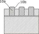
도 1은 (a) 에칭 전 매립된 TSV들 및 (b) 비아 노출 에칭 이후 노출된 TSV를 나타낸다;
도 2는 본 발명을 수행하는데 적합한 장치를 나타낸다;
도 3은 (a) 30초동안 50W이고 이어서 0W 바이어스; (b) 에칭 전체동안 100W 바이어스 및 (c) 사이클 공정으로 에칭된 실리콘의 주사 전자 현미경(SEM) 이미지를 나타낸다;
도 4는 (a) 일반적인 공정 및 (b) 사이클 공정을 사용하여 에칭된 실리콘에 대한 원자력 현미경(AFM) 데이터를 나타낸다.Implementations of the methods according to the present invention will now be described with reference to the accompanying drawings:
Figure 1 shows (a) TSVs buried before etch and (b) exposed TSV after via exposure etch;
Figure 2 shows an apparatus suitable for carrying out the invention;
Figure 3 shows (a) 50W for 30 seconds followed by 0W bias; (b) a scanning electron microscope (SEM) image of silicon etched with a 100 W bias during the entire etch and (c) the cycle process;
4 shows atomic force microscopy (AFM) data for etched silicon using (a) general process and (b) cycle process.
본 발명은 사이클 공정으로 반도체 에칭을 제공한다. 상기 에칭은 바이어스 파워를 이용하여 수행되는 플라즈마 에칭인 제1 에칭 스텝과, 바이어스 파워가 없거나, 낮은 바이어스 파워가 사용되는 제2 에칭 스텝이 교대된다. 본 발명은 이제 TSV 노출 에칭과 연결하여 예시될 것이다. 그러나, 본발명은 다른 에칭 적용에도 활용될 수 있다.The present invention provides semiconductor etching in a cyclic process. The etching alternates between a first etching step, which is plasma etching performed using bias power, and a second etching step, wherein no bias power or low bias power is used. The present invention will now be illustrated in conjunction with TSV exposure etch. However, the present invention can be applied to other etching applications.
도 1은 TSV 노출 실리콘 에칭 공정을 나타낸다. 도 1(a)는 에칭 이전에 실리콘 웨이퍼(12) 내에 매립된 TSV들(10)을 나타낸다. 실리콘 웨이퍼(12)는 접착층(16)에 의해 캐리어 웨이퍼(14)에 결합된다. 캐리어 웨이퍼(14)는 실리콘 또는 유리와 같은 어떤 적합한 물질이 될 수 있다. 에칭은 도 1(b)에 도시된 바와 같이, TSV들(10)을 노출시키도록 수행된다. 각각의 TSV(10)는 보호 산화 라이너(10b)로 코팅된 전기적 전도성 물질(10a)을 포함한다. 전기적 전도성 물질은 일반적으로 구리와 같은 금속이다. 플라즈마의 가혹한 조건에 대하여 아래에 놓인 전기적 전도성 물질(10b)의 노출이 없는 것이 중요하다. 이것은 결국 에칭이 산화물에 대한 높은 실리콘 선택비로 진행되는 공정 요건에 놓인다.Figure 1 shows a TSV exposed silicon etching process. Figure 1 (a) shows the
도 2는 에칭 장치를 나타내는 것으로, 일반적으로 20으로 그려지고, 본 발명의 에칭을 수행하는데 사용될 수 있다. 1차 가스 피드(primary gas feed)(22)가 1차 이온화 소스(26)와 결합된 1차 챔버(24)에 진입한다. RF 안테나(28)은 ICP 소스로 작용한다. 이것은 생성되는 플라즈마의 구속을 수정하기 위하여 DC 코일(30)에 의해 지원될 수 있다. 패러데이 쉴드(Faraday shield)(38)는 용량성 결합(capacitive coupling)을 감소시키기 위해 DC 코일(30) 및 1차 챔버(24)의 벽 사이에 제공될 수 있다. 1차 소스로부터의 플라즈마는 처리된 웨이퍼(34)가 웨이퍼 지지대 판(36), 본 실시예는 정전척(electrostatic chuck) 상에 안착되는 주 챔버(32)에 진입한다. 헬륨의 압력은 냉각 목적을 위하여 정전척의 하측에 인가된다. 주 챔버(32)는 챔버 벽에 인접하여 2차 플라즈마를 제공하기 위하여 주챔버(32) 주위에 배치되는 2차 RF 코일(42)을 포함하는 2차 이온화 소스(40)을 갖는다. RF 코일(30)은 어떤 편리한 주파수, 일반적으로 13.56MHz에서 작동한다. RF 코일(42)는 또한 13.56MHz에서 또는 1-2MHz와 같은 낮은 주파수에서 작동할 수 있다. 환형의 가스 분배 시스템(44)는 2차 플라즈마를 위하여 독립된 가스 소스를 제공하기 위하여 주 챔버(32) 내에 편입된다. 웨이퍼(34)의 가장자리는 WEP(wafer edge protection) 디바이스(46)에 의해 보호될 수 있다. 본 장치는 터보 펌프(50)에 의해 게이트 밸브(48)을 통해 펌핑된다. 바이어스 RF 소스(52)는 RF 신호를 웨이퍼 지지대(26)에 공급하는 데 사용된다. 이 방식에서, 바이어스 파워는 웨이퍼 지지대 판 및 그 결과 웨이퍼(34)에 인가될 수 있다. 2개의 플라즈마를 생성하기 위해 2개의 RF 코일을 갖는, 이 타입의 에칭 장치는 상표명 Pegasus(RTM) 하에서 출원인에 의해 상업적으로 생산될 수 있다. 그러나, 숙련된 기술자는 본 발명이 이러한 타입의 트윈 RF 코일 장치에 제한되지 않는다는 것을 이해할 것이다. 사실, 본 발명은 광범위한 플라즈마 장치에서 시행될 수 있다.Figure 2 shows an etching apparatus, generally depicted as 20, and can be used to perform the etching of the present invention. A primary gas feed (22) enters the primary chamber (24) associated with the primary ionization source (26). The
본 발명은 제1 및 제2 에칭 스텝이 교대로 반복되는 사이클 에칭을 제공한다. 제1 에칭 스텝에서는, RF 소스(52)에 의해 바이어스 파워가 웨이퍼 지지대(36)에 인가된다. 바이어스 파워는 제1 에칭 스텝동안 연속적으로 인가될 수 있고, 이 경우 대략 100W의 파워가 적합한 것을 발견할 수 있다. 그란, 바이어스 파워는 제1 에칭 스텝동안 펄스되는 것이 바람직하다. 펄스 바이어스 파워를 위하여, 20% 듀티 사이클을 갖는 펄스된 500W 파워가 적합한 것을 발견할 수 있다. 제2 에칭 스텝에서는, RF 바이어스 파워가 인가되지 않는 것이 바람직하다. 제1 및 제2 에칭 스텝 각각의 길이는 예상되는 특정 적용에 따라서 선택될 수 있다. 일반적으로, 제1 및 제2 에칭 스텝 각각은 0.5~10초의 범위동안 수행된다. 일반적인 주기는 적어도 공정의 시작에서, 각각의 제1 에칭 스텝에 대하여는 3초이고 제2 에칭 스텝에 대하여는 6초이다. 사이클의 총 수는 식각비 및 타겟 깊이에 의존한다. 요구되는 사이클의 총 수는 미리 정해지거나 에칭 공정의 진척에 따라 제어될 수 있다.The present invention provides a cycle etch wherein the first and second etch steps are alternately repeated. In the first etching step, a bias power is applied to the wafer support table 36 by the
표 1c)는 적용된 공정 조건의 예를 나타낸다. 표 1 a) 및 b)는 비교 데이터 생성에 사용된 공정 조건을 나타낸다.Table 1c) shows examples of applied process conditions. Table 1 a) and b) show the process conditions used for generating the comparison data.

표 1a) 0W 바이어스 공정(BT1 = 에칭 스텝에 앞선 "Breakthrough" 스텝)
Table 1a) 0W bias process (BT1 = Breakthrough step prior to etching step)

표 1b) 100W 바이어스 공정(BT1 = 에칭 스텝에 앞선 "Breakthrough" 스텝)
Table 1b) 100W bias process (BT1 = "Breakthrough" step prior to etching step)

표 1c) 루프 펄스 공정
Table 1c) Loop pulse process
표 1c에 나타난 예에서는, 소스 파워, 가스 플로우, 및 압력 모두 사이클들 간에 동일하게 유지된다. 그러나, 이러한 변수들은 제1 에칭 스텝과 제2 에칭 스텝 간에 달라질 수 있고/있거나 이들은 에칭 공정의 총 시간동안 변화될 수 있다. 또한, 제1 에칭 및/또는 제2 에칭 스텝의 시간 길이는 에칭 공정 진행에 따라 변화될 수 있다. 또한 바이어스 파워가 에칭 공정 진행에 따라 변화될 수 있다. 표 1에 도시된 공정 조건은 높은 식각비(8.5 마이크론/분보다 큰)를 가져온다. 본 발명은 이러한 타입의 높은 식각비 공정에 적용될 수 있는 데 유리하고, 또한 낮은 파워 및 가스 플로우를 사용하는 에칭 공정에 적용될 수 있다.In the example shown in Table 1c, both source power, gas flow, and pressure remain the same between cycles. However, these parameters can vary between the first etching step and the second etching step and / or they can vary during the total time of the etching process. Further, the time length of the first etching and / or the second etching step may be changed according to the progress of the etching process. Further, the bias power can be changed according to the progress of the etching process. The process conditions shown in Table 1 result in a high etch rate (greater than 8.5 microns / minute). The present invention is advantageous in that it can be applied to this type of high etch rate process and can also be applied to etching processes using low power and gas flow.
도 3은 본 발명의 사이클 프로세스가 어떻게 표면 거칠기를 향상시키는지를 보여주는 SEM 이미지를 나타낸다. 실리콘 웨이퍼들은 대략(~) 27 마이크론의 실리콘을 제거하기 위하여 180초동안 대략 9마이크론/분에서 식각되었다. 공정 1a) 및 1b)에서 벌크 에칭에 앞서 짧은 30초 "break through"(BT1) 스텝이 있다. 이는 공정 1c)에는 요구되지 않는다. 이 짧은 스텝은 웨이퍼 표면에서 비연속성을 제거하고 플라즈마 박막 에칭시 널리 사용된다. 도 3(a)는 낮은 바이어스 공정(표 1a 조건)으로 에칭된 실리콘의 SEM 이미지를 나타내고, Si 및 SiO2 식각비 간의 선택비를 최대화하였다. 도 3(b)는 에칭내내 100W의 연속적인 바이어스를 사용하여 에칭된 실리콘의 SEM 이미지를 나타낸다. 예상대로, 현저히 향상된 정도의 표면 거칠기가 관찰되었다. 이 웨이어에 대한 공정 조건은 표 1b)에서 볼 수 있다. 그러나, 아래에 보다 상세하게 설명하는 바와 같이, 이러한 에칭 공정은 받아들이기 어려운 열위의 산화물에 대한 실리콘 선택비를 가져온다. 도 3(c)는 표 1c에 기술된 공정조건을 사용한 본 발명의 사이클 공정에 따라 에칭된 실리콘의 SEM 이미지를 나타낸다. 낮은 거칠기 정도를 갖는, 우수한 표면이 얻어지는 것을 볼 수 있다. 가시적인 가공물(visible artefact)이 없는 것이 관찰될 수 있다. 이는 도 4에 나타낸 AFM 데이터에 의해 확인된다. 도 4(a)는 일반적인 종래 기술 공정 후 얻어지는 AFM 데이터를 나타낸다. 표 1a)에 기술된 높은 선택비 공정 사용에 의해 5.9nm의 표면 거칠기값(Ra)이 관찰된다. 도 4(b)는 표 1c의 공정 조건을 사용하여 에칭된 실리콘을 분석하였을 때 얻어지는 AFM 데이터를 나타낸다. 0.97nm의 측정된 거칠기(Ra)를 갖는 매끄러운 표면 프로파일이 얻어진다.Figure 3 shows an SEM image showing how the cycle process of the present invention improves surface roughness. The silicon wafers were etched at approximately 9 microns / min for 180 seconds to remove approximately (~) 27 microns of silicon. There is a short 30 second "break through" (BT1) step prior to bulk etching in steps 1a) and 1b). This is not required for step 1c). This short step removes discontinuity on the wafer surface and is widely used in plasma thin film etching. Figure 3 (a) shows an SEM image of the etched silicon to a low bias step (Table 1a conditions), followed by maximizing the selectivity between Si and SiO2 etch ratio. Figure 3 (b) shows a SEM image of etched silicon using a continuous bias of 100 W throughout the etch. As expected, a significantly improved surface roughness was observed. The process conditions for this wafer can be seen in Table 1b). However, as will be explained in more detail below, such an etching process results in a silicon selectivity to oxide which is difficult to accept. Figure 3 (c) shows a SEM image of the etched silicon according to the inventive cycling process using the process conditions described in Table 1c. An excellent surface having a low degree of roughness can be obtained. It can be observed that there is no visible artefact. This is confirmed by the AFM data shown in Fig. 4 (a) shows AFM data obtained after a general prior art process. The surface roughness value (Ra) of 5.9 nm is observed by the high selective non-process use described in Table 1a). 4 (b) shows the AFM data obtained when the etched silicon was analyzed using the process conditions of Table 1c. A smooth surface profile with a measured roughness (Ra) of 0.97 nm is obtained.
표 1 a)-c)에 기술된 세가지 공정의 함수로서 에칭 선택비, 식각비 및 거칠기에 대한 결과가 표 2에 나타나 있다.The results for etch selectivity, etch rate, and roughness as a function of the three processes described in Table 1 a) -c) are shown in Table 2.
표 2Table 2

표 2. 표 1에 도시된 세가지 공정에서의 식각비, 선택비 및 표면 거칠기.Table 2. Etch ratio, selectivity and surface roughness in the three processes shown in Table 1.
표 2에 도시된 데이터는 사이클 프로세스(1c)가 100W의 높은 RF 바이어스를 활용한 연속 공정에 비교하여 선택비에서 현저히 향상됨을 명확히 증명한다. 연속된 100W RF 바이어스로 얻어진 선택비(이산화 실리콘에 대한 실리콘) (70:1)은 TSV 노출 에칭에 사용되기에 받아들여질 수 없는 반면, 사이클 공정으로 얻어진 170:1의 이산화실리콘에 대한 실리콘의 향상된 선택비는 TSV 노출 에칭에 사용되기에 받아들여질 수 있다. 이산화실리콘에 대한 실리콘의 높은 선택비는 0W 바이어스 공정으로 얻어지나, 이는 받아들여질 수 없는 열위의 표면 거칠기를 야기한다.The data shown in Table 2 clearly demonstrates that cycle process 1c significantly improves selectivity compared to a continuous process utilizing a high RF bias of 100W. The selectivity (silicon for silicon dioxide) (70: 1) obtained with successive 100W RF biases can not be accepted for use in TSV exposure etch, whereas the improved (100: 1) silicon to 170: 1 silicon dioxide Selection ratios can be accepted for use in TSV exposure etch. The high selectivity of silicon to silicon dioxide is obtained by a 0W bias process, which causes surface roughness of unacceptable dislocations.
본 발명은 비아의 팁(tip)이 노출되었을 때를 감지하는 종료점 감지 시스템(end-point detection system)과 결합될 수 있다. 이 타입의 종료점 감지 시스템은 전체 내용이 여기서는 참조로 포함된 본 발명의 이전 유럽 특허출원 12192364.3에 개시되어 있다. 이 종료점 감지 시스템은 현재의 본 발명에 결합될 수 있다. 현재의 본 발명과 상대적으로 간단한 결합에서, 종료점 감지 시스템은 비아 팁 노출 시간을 기록한다. 보다 정교한 결합에서, 비아 팁 노출 감지는 공정 변수 조정을 시작하는 것에 사용된다. 추가적으로 또는 대안적으로, 최종 반도체 표면 위의 비아의 원하는 노출 높이를 달성하기 위하여 팁이 노출된 후 한정된 수의 사이클이 수행될 수 있다. 이러한 모든 변수는 본 발명의 범위 내에 있다.
The present invention can be combined with an end-point detection system that detects when a tip of a via is exposed. An endpoint detection system of this type is disclosed in the prior European patent application 12192364.3 of the present invention, the entire contents of which are incorporated herein by reference. This endpoint detection system can be combined with the present invention at present. In a relatively simple combination with the present invention, the endpoint detection system records the via tip exposure time. In more sophisticated combinations, via tip exposure detection is used to initiate process variable adjustment. Additionally or alternatively, a limited number of cycles may be performed after the tip is exposed to achieve the desired exposure height of the vias on the final semiconductor surface. All of these variables are within the scope of the present invention.
Claims (22)
Translated fromKorean전기적 바이어스를 생산하기 위해 기판에 바이어스 파워가 인가되는 플라즈마를 이용하여 제1 에칭 스텝을 수행하는 단계;
바이어스 파워없이 또는 상기 제1 에칭 스텝동안 인가되는 바이어스 파워보다 낮은 바이어스 파워로 제2 에칭 스텝을 수행하는 단계; 및
상기 제1 및 제2 에칭 스텝을 교대로 반복하는 단계를 포함하는 방법.A semiconductor substrate etch method for exposing one or more features embedded in a substrate,
Performing a first etching step using a plasma to which bias power is applied to the substrate to produce an electrical bias;
Performing a second etching step with or without bias power at a bias power that is lower than the bias power applied during the first etching step; And
And repeating the first and second etching steps alternately.
상기 바이어스 파워는 상기 제1 에칭 스텝동안 펄스되는(pulsed) 방법.The method according to claim 1,
Wherein the bias power is pulsed during the first etching step.
상기 바이어스 파워는 10~50% 범위의 듀티 사이클로 펄스되는 방법.3. The method of claim 2,
Wherein the bias power is pulsed with a duty cycle in the range of 10 to 50%.
상기 바이어스 파워는 상기 제1 에칭 스텝동안 기판에 연속적으로 인가되는 방법.The method according to claim 1,
Wherein the bias power is continuously applied to the substrate during the first etching step.
상기 제2 에칭 스텝은 플라즈마 에칭 스텝인 방법.5. The method according to any one of claims 1 to 4,
Wherein the second etching step is a plasma etching step.
상기 바이어스 파워 또는 파워는 RF 파워인 방법.4. The method according to any one of the preceding claims,
Wherein the bias power or power is RF power.
상기 반도체 기판은 실리콘인 방법.4. The method according to any one of the preceding claims,
Wherein the semiconductor substrate is silicon.
상기 피처들은 외측 보호층(outer protective layer)을 포함하는 방법.4. The method according to any one of the preceding claims,
Wherein the features comprise an outer protective layer.
상기 외측 보호층은 예를 들어 이산화실리콘인 산화물층인 방법.9. The method of claim 8,
Wherein the outer protective layer is an oxide layer that is, for example, silicon dioxide.
상기 피처들은 비아들(vias)인 방법.4. The method according to any one of the preceding claims,
Wherein the features are vias.
상기 피처들은 TSV들(Through Silicon Vias)인 방법.11. The method of claim 10,
Wherein the features are Through Silicon Vias (TSVs).
상기 TSV들 각각은 이산화실리콘 외측 보호층을 포함하고, 상기 반도체 기판은 실리콘이고, 그리고 상기 제2 에칭 스텝은 100:1보다 큰, 바람직하게는 150:1보다 큰 실리콘 디옥사이드에 대한 실리콘 선택비로 진행하기 위해 바이어스 파워없이 또는 상기 제1 에칭 스텝동안 인가되는 바이어스 파워보다 낮은 바이어스 파워 중 하나로 수행되는 방법.12. The method of claim 11,
Wherein each of the TSVs comprises a silicon dioxide outer protective layer, the semiconductor substrate is silicon and the second etching step proceeds with a silicon selectivity to silicon dioxide greater than 100: 1, preferably greater than 150: 1 The bias power being less than or equal to the bias power applied during the first etching step.
상기 제1 및 제2 에칭 스텝은 원자력 현미경(atomic force microscopy)으로 측정하였을 때 표면 거칠기 Ra가 2nm 이하, 바람직하게는 1nm 이하가 되도록 교대로 반복되는 방법.13. The method according to claim 11 or 12,
Wherein the first and second etching steps are alternately repeated so as to have a surface roughness Ra of 2 nm or less, preferably 1 nm or less, when measured by atomic force microscopy.
상기 제1 및 제2 에칭 스텝은 적어도 10회 교대 반복되는 방법.4. The method according to any one of the preceding claims,
Wherein the first and second etching steps are alternately repeated at least ten times.
상기 제1 및 제2 에칭 스텝은 0.5~10s 범위로 각각 수행되는 방법.4. The method according to any one of the preceding claims,
Wherein the first and second etching steps are each performed in the range of 0.5 to 10 s.
상기 제1 에칭 스텝 및 선택적으로, 제2 에칭 스텝은 SF6와 같은 불소 함유 가스를 이용하여 형성된 플라즈마를 이용하여 수행되는 방법.4. The method according to any one of the preceding claims,
Wherein the first etching step and optionally the second etching step are performed using a plasma formed using a fluorine containing gas such as SF6 .
상기 제2 에칭 스텝은 피처들 에칭과 비교하여 반도체 기판의 에칭에 향상된 선택비를 제공하기 위해 상기 제1 에칭 스텝에 사용된 바이어스 파워보다 낮은 바이어스 파워로 수행되는 방법.4. The method according to any one of the preceding claims,
Wherein the second etching step is performed with a bias power that is lower than the bias power used in the first etching step to provide an improved selectivity to etching of the semiconductor substrate as compared to feature etching.
상기 제2 에칭 스텝은 100:1보다 큰, 바람직하게는 150:1보다 큰 피처에 대한 반도체 기판 선택비를 제공하도록 수행되는 방법.18. The method of claim 17,
Wherein the second etching step is performed to provide a semiconductor substrate selection ratio for features greater than 100: 1, preferably greater than 150: 1.
복수의 공정 변수가 상기 제1 및 제2 에칭 스텝에 관련되고, 상기 공정변수들은 공정 조건이 감지될 때 바뀌는 방법.4. The method according to any one of the preceding claims,
Wherein a plurality of process variables are associated with the first and second etch steps, and wherein the process variables change as process conditions are detected.
상기 감지되는 공정 조건은 피처들의 노출인 방법.20. The method of claim 19,
Wherein the sensed process conditions are exposure of the features.
전기적 바이어스를 생성하기 위해 기판에 바이어스 파워가 인가되는 플라즈마를 이용하여 제1 에칭 스텝을 수행하는 단계;
바이어스 파워없이 또는 상기 제1 에칭 스텝동안 인가되는 바이어스 파워보다 낮은 바이어스 파워로 제2 에칭 스텝을 수행하는 단계; 및
상기 제1 및 제2 에칭 스텝을 교대로 반복하는 단계를 포함하는 방법.A method of etching an unmasked semiconductor substrate,
Performing a first etching step using a plasma to which a bias power is applied to the substrate to generate an electrical bias;
Performing a second etching step with or without bias power at a bias power that is lower than the bias power applied during the first etching step; And
And repeating the first and second etching steps alternately.
챔버;
반도체 기판을 지지하기 위해 챔버 내에 위치하는 기판 지지대;
반도체 기판 에칭에 사용하기 위해 적어도 하나의 플라즈마를 생성하기 위한 적어도 하나의 플라즈마 생성 디바이스;
전기적 바이어스를 생산하기 위해 기판에 인가될 수 있는 바이어스 파워를 공급하기 위한 바이어스 파워 서플라이; 및
상기 플라즈마 생성 디바이스, 상기 바이어스 파워 서플라이 및 선택적으로, 추가의 에칭 디바이스를 제어하도록 구성되는 적어도 하나의 제어 디바이스를 포함하여, 사용에 있어서, 상기 장치가 제1 및 제2 에칭 스텝을 교대로 반복하고, 상기 제1 에칭 스텝은 반도체 기판을 에칭하기 위해 상기 플라즈마 생성 디바이스에 의해 생성된 플라즈마를 사용하고, 상기 제1 에칭 스텝동안 상기 바이어스 파워 서플라이가 펄스 바이어스 파워(pulsed bias power)를 공급하고; 상기 제2 에칭 스텝은 바이어스 파워없이 또는 제1 에칭 스텝동안 공급되는 바이어스 파워보다 낮은 바이어스 파워를 공급하는 상기 바이어스 파워 서플라이로 수행되는 장치.As a semiconductor substrate etching apparatus,
chamber;
A substrate support positioned within the chamber for supporting a semiconductor substrate;
At least one plasma generating device for generating at least one plasma for use in semiconductor substrate etching;
A bias power supply for supplying a bias power that can be applied to the substrate to produce an electrical bias; And
And at least one control device configured to control the plasma generation device, the bias power supply and optionally a further etching device, wherein, in use, the device alternately repeats the first and second etching steps Wherein the first etching step uses a plasma generated by the plasma generating device to etch a semiconductor substrate and during the first etching step the bias power supply supplies a pulsed bias power; Wherein the second etching step is performed with the bias power supply supplying a bias power that is lower than the bias power supplied without bias power or during the first etching step.
Applications Claiming Priority (2)
| Application Number | Priority Date | Filing Date | Title |
|---|---|---|---|
| GB1406135.2 | 2014-04-04 | ||
| GB201406135AGB201406135D0 (en) | 2014-04-04 | 2014-04-04 | Method of etching |
Publications (2)
| Publication Number | Publication Date |
|---|---|
| KR20150115683Atrue KR20150115683A (en) | 2015-10-14 |
| KR102267521B1 KR102267521B1 (en) | 2021-06-18 |
Family
ID=50776862
Family Applications (1)
| Application Number | Title | Priority Date | Filing Date |
|---|---|---|---|
| KR1020150048244AActiveKR102267521B1 (en) | 2014-04-04 | 2015-04-06 | Method of Etching |
Country Status (7)
| Country | Link |
|---|---|
| US (1) | US9842772B2 (en) |
| EP (1) | EP2927938B1 (en) |
| JP (1) | JP6553391B2 (en) |
| KR (1) | KR102267521B1 (en) |
| CN (1) | CN104979153B (en) |
| GB (1) | GB201406135D0 (en) |
| TW (1) | TWI654651B (en) |
Cited By (1)
| Publication number | Priority date | Publication date | Assignee | Title |
|---|---|---|---|---|
| KR20180064312A (en)* | 2016-12-05 | 2018-06-14 | 에스피티에스 테크놀러지스 리미티드 | Method of smoothing a surface |
Families Citing this family (6)
| Publication number | Priority date | Publication date | Assignee | Title |
|---|---|---|---|---|
| GB201608926D0 (en)* | 2016-05-20 | 2016-07-06 | Spts Technologies Ltd | Method for plasma etching a workpiece |
| CN108538765B (en)* | 2018-05-08 | 2020-10-16 | 国家纳米科学中心 | Etching device and pattern transfer method |
| CN110890277B (en)* | 2018-09-07 | 2022-05-10 | 无锡华润上华科技有限公司 | Preparation method of groove type metal oxide semiconductor Schottky barrier transistor |
| US11355394B2 (en)* | 2018-09-13 | 2022-06-07 | Applied Materials, Inc. | Wafer dicing using hybrid laser scribing and plasma etch approach with intermediate breakthrough treatment |
| CN112522672B (en)* | 2020-11-18 | 2022-05-17 | 东莞市华升真空镀膜科技有限公司 | High-energy pulse magnetic control film coating machine with unbalanced magnetic field and manufacturing and processing technology thereof |
| GB202319607D0 (en) | 2023-12-20 | 2024-01-31 | Spts Technologies Ltd | A method of packaging semiconductor dies |
Citations (4)
| Publication number | Priority date | Publication date | Assignee | Title |
|---|---|---|---|---|
| EP1420438A2 (en)* | 2002-11-15 | 2004-05-19 | Applied Materials, Inc. | Method and apparatus for etching a deep trench |
| KR100594209B1 (en)* | 1999-12-23 | 2006-07-03 | 삼성전자주식회사 | Trench etching method for trench isolation |
| JP2011100760A (en)* | 2009-11-04 | 2011-05-19 | Ulvac Japan Ltd | Etching method |
| JP2013131652A (en)* | 2011-12-21 | 2013-07-04 | Fujitsu Semiconductor Ltd | Semiconductor device manufacturing method, semiconductor wafer processing method, and semiconductor wafer |
Family Cites Families (10)
| Publication number | Priority date | Publication date | Assignee | Title |
|---|---|---|---|---|
| JPH11330059A (en) | 1998-03-19 | 1999-11-30 | Hitachi Ltd | Dry etching equipment |
| JP2000294539A (en)* | 1999-04-05 | 2000-10-20 | Hitachi Ltd | Surface treatment method |
| KR100292412B1 (en) | 1999-07-14 | 2001-06-01 | 윤종용 | Method for enhancing etching selectivity of metal silicide film/polysilicon film and method for etching stacked film of metal silicide film and polysilicon film using the same |
| GB0516054D0 (en)* | 2005-08-04 | 2005-09-14 | Trikon Technologies Ltd | A method of processing substrates |
| US7718538B2 (en) | 2007-02-21 | 2010-05-18 | Applied Materials, Inc. | Pulsed-plasma system with pulsed sample bias for etching semiconductor substrates |
| EP2151509A1 (en)* | 2008-08-04 | 2010-02-10 | Applied Materials, Inc. | Reactive gas distributor, reactive gas treatment system, and reactive gas treatment method |
| JP5558224B2 (en) | 2010-06-23 | 2014-07-23 | 東京エレクトロン株式会社 | Substrate processing method |
| JP5845754B2 (en) | 2010-09-15 | 2016-01-20 | 東京エレクトロン株式会社 | Plasma etching processing method |
| US8735291B2 (en) | 2011-08-25 | 2014-05-27 | Tokyo Electron Limited | Method for etching high-k dielectric using pulsed bias power |
| US8709268B2 (en) | 2011-11-14 | 2014-04-29 | Spts Technologies Limited | Etching apparatus and methods |
- 2014
- 2014-04-04GBGB201406135Apatent/GB201406135D0/ennot_activeCeased
- 2015
- 2015-04-01TWTW104110720Apatent/TWI654651B/enactive
- 2015-04-02EPEP15162490.5Apatent/EP2927938B1/enactiveActive
- 2015-04-03CNCN201510158770.3Apatent/CN104979153B/enactiveActive
- 2015-04-03USUS14/678,048patent/US9842772B2/enactiveActive
- 2015-04-03JPJP2015076920Apatent/JP6553391B2/enactiveActive
- 2015-04-06KRKR1020150048244Apatent/KR102267521B1/enactiveActive
Patent Citations (4)
| Publication number | Priority date | Publication date | Assignee | Title |
|---|---|---|---|---|
| KR100594209B1 (en)* | 1999-12-23 | 2006-07-03 | 삼성전자주식회사 | Trench etching method for trench isolation |
| EP1420438A2 (en)* | 2002-11-15 | 2004-05-19 | Applied Materials, Inc. | Method and apparatus for etching a deep trench |
| JP2011100760A (en)* | 2009-11-04 | 2011-05-19 | Ulvac Japan Ltd | Etching method |
| JP2013131652A (en)* | 2011-12-21 | 2013-07-04 | Fujitsu Semiconductor Ltd | Semiconductor device manufacturing method, semiconductor wafer processing method, and semiconductor wafer |
Non-Patent Citations (1)
| Title |
|---|
| Dave Thomas et al. "Plasma Etch and Low Temperature PECVD Processes for Via Reveal Applications". Proceedings of 2012 IEEE 62nd Electronic Components and Technology Conference, 2012년 6월 1일, pp. 1662-1667 (2012.06.01.) 1부.** |
Cited By (1)
| Publication number | Priority date | Publication date | Assignee | Title |
|---|---|---|---|---|
| KR20180064312A (en)* | 2016-12-05 | 2018-06-14 | 에스피티에스 테크놀러지스 리미티드 | Method of smoothing a surface |
Also Published As
| Publication number | Publication date |
|---|---|
| EP2927938B1 (en) | 2020-08-19 |
| GB201406135D0 (en) | 2014-05-21 |
| JP2015201643A (en) | 2015-11-12 |
| KR102267521B1 (en) | 2021-06-18 |
| TW201601190A (en) | 2016-01-01 |
| CN104979153B (en) | 2018-11-09 |
| CN104979153A (en) | 2015-10-14 |
| JP6553391B2 (en) | 2019-07-31 |
| US9842772B2 (en) | 2017-12-12 |
| US20150287637A1 (en) | 2015-10-08 |
| TWI654651B (en) | 2019-03-21 |
| EP2927938A1 (en) | 2015-10-07 |
Similar Documents
| Publication | Publication Date | Title |
|---|---|---|
| KR102267521B1 (en) | Method of Etching | |
| CN102956473B (en) | Rising the method for the conformal amorphous carbon film of height of deposition in feature | |
| Wu et al. | High aspect ratio silicon etch: A review | |
| US8889024B2 (en) | Plasma etching method | |
| TWI687549B (en) | Even tungsten etch for high aspect ratio trenches | |
| US8987140B2 (en) | Methods for etching through-silicon vias with tunable profile angles | |
| CN109983558B (en) | Film forming apparatus and film forming method | |
| JP2013070073A (en) | Plasma processing apparatus | |
| US20030022512A1 (en) | Plasma etching method | |
| JP2010021442A (en) | Plasma processing method and apparatus | |
| JP5367689B2 (en) | Plasma processing method | |
| JP2018006773A (en) | Plasma etching method | |
| JP2009302181A (en) | Plasma etching method, and plasma etching apparatus | |
| JP6579786B2 (en) | Plasma etching method | |
| JP5065726B2 (en) | Dry etching method | |
| JP2020177958A (en) | Substrate processing method and substrate processing equipment | |
| JP5284679B2 (en) | Plasma etching method | |
| JP2024545648A (en) | Remote Source Pulsing Using Advanced Pulse Control | |
| JP5961794B2 (en) | Method for manufacturing silicon substrate having concavo-convex structure with high aspect ratio | |
| CN114695105A (en) | Method and apparatus | |
| Laermer et al. | Through-silicon vias using Bosch DRIE process technology | |
| US20250299962A1 (en) | Method for etching a layer through a patterned mask layer |
Legal Events
| Date | Code | Title | Description |
|---|---|---|---|
| PA0109 | Patent application | Patent event code:PA01091R01D Comment text:Patent Application Patent event date:20150406 | |
| PG1501 | Laying open of application | ||
| PA0201 | Request for examination | Patent event code:PA02012R01D Patent event date:20200403 Comment text:Request for Examination of Application Patent event code:PA02011R01I Patent event date:20150406 Comment text:Patent Application | |
| PA0302 | Request for accelerated examination | Patent event date:20200403 Patent event code:PA03022R01D Comment text:Request for Accelerated Examination Patent event date:20150406 Patent event code:PA03021R01I Comment text:Patent Application | |
| E902 | Notification of reason for refusal | ||
| PE0902 | Notice of grounds for rejection | Comment text:Notification of reason for refusal Patent event date:20200729 Patent event code:PE09021S01D | |
| E902 | Notification of reason for refusal | ||
| PE0902 | Notice of grounds for rejection | Comment text:Notification of reason for refusal Patent event date:20201123 Patent event code:PE09021S01D | |
| E701 | Decision to grant or registration of patent right | ||
| PE0701 | Decision of registration | Patent event code:PE07011S01D Comment text:Decision to Grant Registration Patent event date:20210319 | |
| GRNT | Written decision to grant | ||
| PR0701 | Registration of establishment | Comment text:Registration of Establishment Patent event date:20210615 Patent event code:PR07011E01D | |
| PR1002 | Payment of registration fee | Payment date:20210615 End annual number:3 Start annual number:1 | |
| PG1601 | Publication of registration |