KR20150111390A - Thin Film Transistor comprising double layer gate insulator and fabricating method thereof - Google Patents
Thin Film Transistor comprising double layer gate insulator and fabricating method thereofDownload PDFInfo
- Publication number
- KR20150111390A KR20150111390AKR1020140032709AKR20140032709AKR20150111390AKR 20150111390 AKR20150111390 AKR 20150111390AKR 1020140032709 AKR1020140032709 AKR 1020140032709AKR 20140032709 AKR20140032709 AKR 20140032709AKR 20150111390 AKR20150111390 AKR 20150111390A
- Authority
- KR
- South Korea
- Prior art keywords
- oxide
- insulating film
- thin film
- gate
- layer
- Prior art date
- Legal status (The legal status is an assumption and is not a legal conclusion. Google has not performed a legal analysis and makes no representation as to the accuracy of the status listed.)
- Withdrawn
Links
Images


Classifications
- H—ELECTRICITY
- H10—SEMICONDUCTOR DEVICES; ELECTRIC SOLID-STATE DEVICES NOT OTHERWISE PROVIDED FOR
- H10D—INORGANIC ELECTRIC SEMICONDUCTOR DEVICES
- H10D30/00—Field-effect transistors [FET]
- H10D30/60—Insulated-gate field-effect transistors [IGFET]
- H10D30/67—Thin-film transistors [TFT]
- H10D30/674—Thin-film transistors [TFT] characterised by the active materials
- H10D30/6755—Oxide semiconductors, e.g. zinc oxide, copper aluminium oxide or cadmium stannate
- H—ELECTRICITY
- H10—SEMICONDUCTOR DEVICES; ELECTRIC SOLID-STATE DEVICES NOT OTHERWISE PROVIDED FOR
- H10D—INORGANIC ELECTRIC SEMICONDUCTOR DEVICES
- H10D30/00—Field-effect transistors [FET]
- H10D30/60—Insulated-gate field-effect transistors [IGFET]
- H10D30/67—Thin-film transistors [TFT]
- H10D30/6758—Thin-film transistors [TFT] characterised by the insulating substrates
Landscapes
- Thin Film Transistor (AREA)
Abstract
Description
Translated fromKorean본 발명은 반도체 소자에 관한 것으로서, 더욱 상세하게는, 이중층 게이트 절연막을 포함하는 박막 트랜지스터 및 이의 제조 방법에 관한 것이다.The present invention relates to a semiconductor device, and more particularly, to a thin film transistor including a double-layer gate insulating film and a method of manufacturing the same.
금속 산화물 박막 트랜지스터(Thin Film Transistor: TFT)는 높은 이동성(mobility), 가시광선에 대한 투명성, 비정질 실리콘 박막 트랜지스터에 비하여 저온 공정이 가능한 장점으로 인하여 구부릴 수 있는 즉, 가요성 있는 접이식 및/또는 투명 정보 디스플레이용 스위칭 소자로 주목 받는 반도체 소자이다. 상기 가요성 디스플레이에 플라스틱 기판을 사용하기 위하여는, 증착 및 열처리 등의 모든 처리 공정은 플라스틱 기판의 변형 또는 휘어짐을 방지하기 위하여 250 ℃ 이하의 저온에서 수행되어야만 한다.Metal oxide thin film transistors (TFTs) have advantages of high mobility, transparency to visible light, and low temperature processability compared to amorphous silicon thin film transistors, so that flexible, foldable and / or transparent And is a semiconductor device noticed as a switching device for information display. In order to use a plastic substrate for the flexible display, all processes such as deposition and heat treatment must be performed at a low temperature of 250 ° C or less to prevent deformation or warping of the plastic substrate.
종래의 스퍼터링된 반도체 산화막은 실온에서 제조될 수 있기 때문에 금속 산화물 반도체의 경우, 높은 이동성을 갖는 플라스틱 호환 금속 산화물 채널층을 제조하는 것이 간단하다. 그러나, SiO2와 같은 고품질의 게이트 유전체층은 고가의 진공 기반의 PECVD 시스템을 사용하여 300 ℃ 이상의 고온에서 증착되어야 한다. 최근에는 Al2O3, Y2O3, HfO2 및 ZrO2를 포함하는 습식 공정의 게이트 유전체층이 저비용의 제조를 위하여 집중적으로 연구되고 있다. 습식 공정의 게이트 유전체를 갖는 금속 산화물 박막 트랜지스터가 좋은 성과를 달성한다 하더라도, 300℃ 이상의 높은 어닐링 온도는 합리적인 게이트 누설 전류 및 낮은 오프-상태 드레인 전류를 제공하기 위하여 여전히 요구된다.Since conventional sputtered semiconductor oxide films can be manufactured at room temperature, it is simple to fabricate a plastic-compatible metal oxide channel layer with high mobility in the case of metal oxide semiconductors. However, a high quality gate dielectric layer, such as SiO2 , must be deposited at a high temperature above 300 ° C using an expensive vacuum-based PECVD system. Recently, a wet process gate dielectric layer comprising Al2 O3 , Y2 O3 , HfO2 and ZrO2 has been intensively studied for low cost fabrication. Although metal oxide thin film transistors with gate dielectrics in wet processes achieve good results, high annealing temperatures above 300 DEG C are still required to provide a reasonable gate leakage current and low off-state drain current.
또한, 플렉시블 디스플레이에서 이용되기 위하여 박막 트랜지스터는 1mm 이하의 두께로 구부러지거나 접힐 수 있어야 한다. 이 경우, 채널 및 전극 영역과 같은 분리막 보다는 게이트 절연막과 같은 접촉되는 막에서 기계적인 결함이 더 많이 발생된다. 그러므로, 기계적 안정성의 관점에서 고분자 유기막을 금속 산화물 박막 트랜지스터의 절연막에 이용하는 것이 바람직하다.Further, in order to be used in a flexible display, a thin film transistor must be bent or folded to a thickness of 1 mm or less. In this case, more mechanical defects are generated in the contact film, such as the gate insulating film, than the separation film such as the channel and the electrode region. Therefore, from the viewpoint of mechanical stability, it is preferable to use the polymer organic film for the insulating film of the metal oxide thin film transistor.
그러나, 유기물 절연막은 고온 처리가 불가능하다는 문제가 있으며, 절연막의 표면을 개질하기 위하여 유기 용매를 사용시, 유기물 절연막의 표면 특성을 오히려 저하시키는 문제점이 있다. 또한, 유기물 절연막을 소자 제조에 이용하는 경우 소자가 히스테리시스(hysteresis)를 보일 수 있는 단점이 존재한다.However, there is a problem that the organic insulating film can not be treated at high temperature, and when using an organic solvent for modifying the surface of the insulating film, the surface characteristics of the organic insulating film are rather deteriorated. In addition, when an organic insulating film is used in the manufacture of a device, there is a disadvantage that the device can exhibit hysteresis.
따라서, 본 발명이 해결하고자 하는 기술적 과제는, 이동도, 서브문턱 게이트 스윙, 문턱 전압, 및 Ion/off 와 같은 소자의 특성을 개선시키는 재료 및 구조로 제조된 이중층 게이트 절연막을 포함하는 박막 트랜지스터를 제공하는 것이다.SUMMARY OF THE INVENTION Accordingly, it is an object of the present invention to provide a thin film transistor including a dual-layer gate insulating film made of materials and structures that improve device characteristics such as mobility, sub-threshold gate swing, threshold voltage, and Ion / .
또한, 본 발명이 해결하고자 하는 다른 기술적 과제는, 저온 습식 공정으로 플렉시블한 특성을 갖고, 산화물 반도체와 계면특성이 좋은 이중층 게이트 절연막을 포함하는 박막 트랜지스터를 제조하는 방법을 제공하는 것이다.Another object of the present invention is to provide a method of manufacturing a thin film transistor including a double-layer gate insulating film having a flexible characteristic in a low-temperature wet process and having good oxide semiconductor and interface characteristics.
상기 기술적 과제를 해결하기 위한 박막 트랜지스터는 인듐(In), 아연(Zn), 주석(Sn), 알루미늄(Al), 마그네슘(Mg), 하프늄(Hf), 갈륨(Ga), 및 타이타늄(Ti) 중 적어도 어느 하나의 산화물을 포함하는 활성층; 상기 활성층 상에 배치되는 게이트 절연막; 상기 게이트 절연막을 사이에 두고 상기 활성층의 적어도 일부와 중첩되는 게이트 도전막; 및 상기 도전막에 의해 이격된 상기 활성층의 양 측부들에 형성된 소오스 및 드레인 영역들을 포함하는 박막 트랜지스터를 포함하고, 상기 게이트 절연막은 실리콘(Si)을 포함하는 전기적 특성이 우수한 하부 절연막; 및 아연(Zn), 지르코늄(Zr), 하프늄(Hf), 알루미늄(Al), 타이타늄(Ti) 및 란터넘(La) 중 적어도 어느 하나의 산화물을 포함하는 유전 특성이 우수한 상부 절연막을 포함할 수 있다.In order to achieve the above object, the present invention provides a thin film transistor comprising at least one of indium, zinc, tin, aluminum, magnesium, hafnium, gallium, and titanium, An active layer containing at least one of oxides; A gate insulating film disposed on the active layer; A gate conductive layer overlapping at least a part of the active layer with the gate insulating film interposed therebetween; AndAnd a thin film transistor including source and drain regions formed on both sides of the active layer spaced apart by the conductive film, wherein the gate insulating film includes a lower insulating film including silicon (Si) and having excellent electrical characteristics; And an upper insulating film containing an oxide of at least one of zinc (Zn), zirconium (Zr), hafnium (Hf), aluminum (Al), titanium (Ti) and lanthanum have.
상기 박막 트랜지스터는 상기 활성층 상에 순차대로 상기 게이트 절연막 및 상기 게이트 도전막이 형성되는 상부 게이트 구조를 가질 수 있다. 또는, 상기 박막 트랜지스터는 상기 게이트 도전막 상에 순차적으로 상기 게이트 절연막 및 상기 활성층이 형성되는 하부 게이트 구조를 가질 수 있다.The thin film transistor may have a top gate structure in which the gate insulating film and the gate conductive film are sequentially formed on the active layer. Alternatively, the thin film transistor may have a bottom gate structure in which the gate insulating film and the active layer are sequentially formed on the gate conductive film.
상기 하부 절연막은 실리콘 산화물이고, 상기 상부 절연막은 상기 실리콘 산화물보다 높은 유전율을 갖는 고유전율 유전체를 포함할 수 있다.The lower insulating layer may be a silicon oxide layer, and the upper insulating layer may include a high dielectric constant dielectric layer having a higher dielectric constant than the silicon oxide layer.
상기 하부 절연막은 1㎛ 내지 10mm의 두께를 가지고, 상기 상부 절연체는 1㎛ 내지 10mm의 두께를 가질 수 있다.The lower insulating layer may have a thickness of 1 to 10 mm, and the upper insulating layer may have a thickness of 1 to 10 mm.
상기 소오스 및 드레인 전극들 중 적어도 어느 하나는 투명 도전성 산화물 박막을 포함할 수 있다.At least one of the source and drain electrodes may include a transparent conductive oxide thin film.
상기 투명 도전성 산화물 박막은, 인듐-아연-산화물(Induim-Zinc-Oxide; IZO), 인듐-주석-산화물(Indium-Tin-Oxide; ITO), 불화 주석 산화물(Fluorinated Tin Oxide; FTO), 인듐 산화물(Indium Oxide; IO) 및 주석 산화물(Tin Oxide; SnO2) 중 어느 하나 또는 이들의 조합을 포함할 수 있다.The transparent conductive oxide thin film may include at least one selected from the group consisting of Indium-Zinc-Oxide (IZO), Indium-Tin-Oxide (ITO), Fluorinated Tin Oxide (Indium Oxide) and tin oxide (SnO2), or a combination thereof.
상기 다른 기술적 과제를 해결하기 위한 박막 트랜지스터의 제조 방법은, 활성층 상에 배치되는 게이트 절연막을 통하여 상기 활성층의 적어도 일부와 중첩되는 게이트 도전막; 및 상기 게이트 도전막에 의해 이격된 상기 활성층의 양 측부들에 각각 접속되는 소오스 및 드레인 전극들을 포함하는 박막 트랜지스터의 제조 방법으로서, 상기 박막 트랜지스터가 형성될 기판을 제공하는 단계; 상기 기판 상에 실리콘 산화물을 포함하는 하부 절연막을 형성하는 단계; 및 상기 하부 절연막 상에 아연(Zn), 지르코늄(Zr), 하프늄(Hf), 알루미늄(Al), 타이타늄(Ti) 및 란터넘(La) 중 적어도 어느 하나의 산화물을 포함하는 유전 특성이 우수한 상부 절연막을 포함할 수 있다.
According to another aspect of the present invention, there is provided a method of manufacturing a thin film transistor, including: forming a gate conductive layer over a gate insulating layer disposed on an active layer to overlap with at least a portion of the active layer; And source and drain electrodes respectively connected to both sides of the active layer spaced apart by the gate conductive film, the method comprising: providing a substrate on which the thin film transistor is to be formed; Forming a lower insulating film including silicon oxide on the substrate; And an upper dielectric layer including an oxide of at least one of zinc (Zn), zirconium (Zr), hafnium (Hf), aluminum (Al), titanium (Ti), and lanthanum (La) And may include an insulating film.
본 발명의 실시예에 따르면, 실리콘 산화물 및 무기 절연체를 포함하는 다층 절연막을 포함함으로서, 서브문턱 게이트 스윙(subthreshold swing), 및 문턱전압(threshold voltage)과 같은 성능이 향상된 박막 트랜지스터를 제공할 수 있다.According to the embodiment of the present invention, it is possible to provide a thin film transistor having improved performance such as a subthreshold swing and a threshold voltage by including a multilayer insulating film including silicon oxide and an inorganic insulator .
본 발명의 다른 실시예에 따르면, 용액 공정을 이용하여 게이트 절연막을 형성함으로써 플렉시블하고 안정된 소자 특성을 갖는 박막 트랜지스터를 제조하는 방법을 제공할 수 있다. 또한, 다층 게이트 절연막을 형성함으로써 낮은 공정온도에서도 채널과의 계면특성이 향상되어 낮은 서브문턱 게이트 스윙 값을 갖고, 형성 두께를 조절할 수 있어 누설 전류를 감소시킬 수 있는 박막 트랜지스터의 제조 방법을 제공할 수 있다.
According to another embodiment of the present invention, a method of manufacturing a thin film transistor having a flexible and stable device characteristic can be provided by forming a gate insulating film using a solution process. Also, by providing a multi-layered gate insulating film, it is possible to provide a thin film transistor manufacturing method capable of improving the interfacial characteristics with the channel at low process temperatures, having a low sub-threshold gate swing value, .
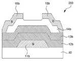
도 1a 및 도 1b는 본 발명의 일 실시예에 따른 박막 트랜지스터들을 각각 도시하는 단면도이다.
도 2a 내지 도 2c는 본 발명의 비교예 1, 2 및 실험예에 따른 박막 트랜지스터의 소스-드레인 전류를 나타낸다.
도 3a 및 도 3b는 본 발명의 비교예 1 및 실험예의 게이트 절연막의 원자현미경(AFM) 이미지이다.1A and 1B are cross-sectional views respectively showing thin film transistors according to an embodiment of the present invention.
2A to 2C show the source-drain currents of the thin film transistors according to Comparative Examples 1 and 2 and Experimental Example of the present invention.
3A and 3B are atomic force microscope (AFM) images of the gate insulating film of Comparative Example 1 and Experimental Example of the present invention.
이하, 본 발명을 실시예를 통하여 보다 상세하게 설명한다.Hereinafter, the present invention will be described in more detail with reference to examples.
본 발명의 실시예들은 당해 기술 분야에서 통상의 지식을 가진 자에게 본 발명은 더욱 완전하게 설명하기 위하여 제공되는 것이며, 하기 실시예는 여러 가지 다른 형태로 변형되는 수 있으며, 본 발명의 범위가 하기 실시예에 한정되는 것은 아니다. 오히려, 이들 실시예는 본 개시를 더욱 충실하고 완전하게 하고, 당업자에게 본 발명의 사상을 완전하게 전달하기 위하여 제공되는 것이다.It is to be understood that both the foregoing general description and the following detailed description are exemplary and explanatory and are intended to provide further explanation of the invention as claimed and will become apparent to those skilled in the art. It is not limited to the embodiment. Rather, these embodiments are provided so that this disclosure will be more faithful and complete, and will fully convey the scope of the invention to those skilled in the art.
또한, 이하의 도면에서 각 층의 두께나 크기는 설명의 편의 및 명확성을 위하여 과장된 것이며, 도면상에서 동일 부호는 동일한 요소를 지칭한다. 본 명세서에서 사용된 바와 같이, 용어 "및/또는" 는 해당 열거된 항목 중 어느 하나 및 하나 이상의 모든 조합을 포함한다.In the following drawings, thickness and size of each layer are exaggerated for convenience and clarity of description, and the same reference numerals denote the same elements in the drawings. As used herein, the term "and / or" includes any and all combinations of any of the listed items.
본 명세서에서 사용된 용어는 특정 실시예를 설명하기 위하여 사용되며, 본 발명을 제한하기 위한 것이 아니다. 본 명세서에서 사용된 바와 같이, 단수 형태는 문맥상 다른 경우를 분명히 지적하는 것이 아니라면, 복수의 형태를 포함할 수 있다. 또한, 본 명세서에서 사용되는 경우 "포함한다(comprise)" 및/또는 "포함하는(comprising)"은 언급한 형상들, 숫자, 단계, 동작, 부재, 요소 및/또는 이들 그룹의 존재를 특정하는 것이며, 하나 이상의 다른 형상, 숫자, 동작, 부재, 요소 및/또는 그룹들의 존재 또는 부가를 배제하는 것이 아니다.The terminology used herein is for the purpose of describing particular embodiments only and is not intended to be limiting of the invention. As used herein, the singular forms "a," "an," and "the" include singular forms unless the context clearly dictates otherwise. Also, " comprise "and / or" comprising "when used herein should be interpreted as specifying the presence of stated shapes, numbers, steps, operations, elements, elements, and / And does not preclude the presence or addition of one or more other features, integers, operations, elements, elements, and / or groups.
이하의 설명에서 어떤 층이 다른 층 "상에(on)"형성된다고 기술될 때, 이는 다른 층의 바로 위에 형성된 층을 지칭하거나, 다른 층 상에 형성된 중간 층 또는 중간 층들 상에 형성된 층을 지칭할 수도 있다. 또한, 당해 기술 분야에서 숙련된 자들에게 있어서, 다른 형상에 "인접하여(adjacent)" 배치된 구조 또는 형상은 상기 인접하는 형상에 중첩되거나 하부에 배치되는 부분을 가질 수도 있다.In the following description, when a layer is described as being "on" another layer, it refers to a layer formed directly on top of another layer, or to a layer formed on an intermediate or intermediate layer formed on another layer You may. It will also be appreciated by those skilled in the art that structures or shapes that are "adjacent" to other features may have portions that overlap or are disposed below the adjacent features.
본 명세서에서, "아래로(below)", "위로(above)", "상부의(upper)", "하부의(lower)", "수평의(horizontal)" 또는 "수직의(vertical)"와 같은 상대적 용어들은, 도면들 상에 도시된 바와 같이, 일 구성 부재, 층 또는 영역들이 다른 구성 부재, 층 또는 영역과 갖는 관계를 기술하기 위하여 사용될 수 있다. 이들 용어들은 도면들에 표시된 방향뿐만 아니라 소자의 다른 방향들도 포괄하는 것임을 이해하여야 한다.As used herein, the terms "below," "above," "upper," "lower," "horizontal," or " May be used to describe the relationship of one constituent member, layer or regions with other constituent members, layers or regions, as shown in the Figures. It is to be understood that these terms encompass not only the directions indicated in the Figures but also the other directions of the devices.
본 명세서에서 사용된 용어는 특정 실시예를 설명하기 위하여 사용되며, 본 발명을 제한하기 위한 것이 아니다. 본 명세서에서 사용된 바와 같이, 단수 형태는 문맥상 다른 경우를 분명히 지적하는 것이 아니라면, 복수의 형태를 포함할 수 있다. 또한, 본 명세서에서 사용되는 경우 "포함한다(comprise)" 및/또는 "포함하는(comprising)"은 언급한 형상들, 숫자, 단계, 동작, 부재, 요소 및/또는 이들 그룹의 존재를 특정하는 것이며, 하나 이상의 다른 형상, 숫자, 동작, 부재, 요소 및 /또는 그룹들의 존재 또는 부가를 배제하는 것이 아니다.The terminology used herein is for the purpose of describing particular embodiments only and is not intended to be limiting of the invention. As used herein, the singular forms "a," "an," and "the" include singular forms unless the context clearly dictates otherwise. Also, " comprise "and / or" comprising "when used herein should be interpreted as specifying the presence of stated shapes, numbers, steps, operations, elements, elements, and / And does not preclude the presence or addition of one or more other features, integers, operations, elements, elements, and / or groups.
본 명세서에서 제 1, 제 2 등의 용어가 다양한 부재, 부품, 영역, 층들 및/또는 부분들을 설명하기 위하여 사용되지만, 이들 부재, 부품, 영역, 층들 및/또는 부분들은 이들 용어에 의해 한정되어서는 안됨은 자명하다. 이들 용어는 하나의 부재, 부품, 영역, 층 또는 부분을 다른 영역, 층 또는 부분과 구별하기 위하여만 사용된다. 따라서, 이하 상술할 제 1 부재, 부품, 영역, 층 또는 부분은 본 발명의 가르침으로부터 벗어나지 않고서도 제 2 부재, 부품, 영역, 층 또는 부분을 지칭할 수 있다.Although the terms first, second, etc. are used herein to describe various elements, components, regions, layers and / or portions, these members, components, regions, layers and / It is obvious that no. These terms are only used to distinguish one member, component, region, layer or section from another region, layer or section. Thus, a first member, component, region, layer or section described below may refer to a second member, component, region, layer or section without departing from the teachings of the present invention.
본 명세서에서 사용된 "비정징 구조"라는 용어는 일반적으로 원자들이 분명한 주기적 배열을 결여하고 있는 낮은 정도의 질서도를 갖는 비결정질 구조를 의미하며, 이는 상기 비결정질 구조 내에 마이크로 결정이 형성된 구조도 포함하는 것으로 해석되어야 한다.As used herein, the term " unstructured structure "generally refers to an amorphous structure having a low degree of orderliness in which atoms lack definite periodic arrangements, including structures in which microcrystals are formed in the amorphous structure .
이하에서, 본 발명의 실시예들은 본 발명의 이상적인 실시예들(및 중간 구조들)을 개략적으로 도시하는 단면도들을 참조하여 설명될 것이다. 이들 도면들에 있어서, 예를 들면, 부재들의 크기와 형상은 설명의 편의와 명확성을 위하여 과장될 수 있으며, 실제 구현시, 도시된 형상의 변형들이 예상될 수 있다. 따라서, 본 발명의 실시예는 본 명세서에 도시된 영역의 특정 형상에 제한된 것으로 해석되어서는 아니 된다. 또한, 도면의 부재들의 참조 부호는 도면 전체에 걸쳐 동일한 부재를 지칭한다.
In the following, embodiments of the present invention will be described with reference to cross-sectional views schematically illustrating ideal embodiments (and intermediate structures) of the present invention. In these figures, for example, the size and shape of the members may be exaggerated for convenience and clarity of explanation, and in actual implementation, variations of the illustrated shape may be expected. Accordingly, embodiments of the present invention should not be construed as limited to any particular shape of the regions shown herein. In addition, reference numerals of members in the drawings refer to the same members throughout the drawings.
도 1a 및 도 1b는 본 발명의 일 실시예에 따른 박막 트랜지스터들을 각각 도시하는 단면도이다.1A and 1B are cross-sectional views respectively showing thin film transistors according to an embodiment of the present invention.
도 1a 및 도 1b를 참조하면, 기판(10)상에 박막 트랜지스터(100, 200)가 형성된다. 기판(10)은 박막 트랜지스터(100, 200)의 형성 공정과 양립할 수 있으며, 박막 트랜지스터(100, 200)가 형성될 절연성 표면을 제공할 수 있는 재료로부터 선택될 수 있다. 예를 들면, 기판(10)은 통상의 반도체 제조 공정이 가능한 Si 또는 Ge와 같은 Ⅳ족 반도체, SiGe와 같은 혼합 반도체, GaAs과 같은 Ⅲ-Ⅴ족 화합물 반도체, 또는 CdS와 같은 Ⅱ-Ⅵ족 반도체 재료로 형성될 수 있다. 그러나, 이들은 예시적일 뿐, 본 발명은 이에 제한되지 않으며, 예를 들면, 기판(10)은 알루미늄 산화물과 같은 세라믹 재료 또는 절연막으로 코팅된 금속 시트로 형성될 수도 있다.Referring to FIGS. 1A and 1B,
일부 실시예에서, 기판(10)은 투광성 재료일 수 있다. 상기 투과성 재료는 유리 또는 수지계 재료일 수 있다. 수지계 재료로 형성된 기판은 가요성(flexibility)을 갖기 때문에 바람직하다. 상기 수지계 재료는, 폴리에틸렌 나프탈레이트(polyethylene naphthalate; PEN)와 같은 폴리에스테르 수지; 폴리에틸렌 수지; 염화 폴리비닐 수지; 폴리카보네이트(PC); 폴리에테리 술폰(PES); 폴리에테르 에테르케톤(PEEK); 및 황화 폴리페닐렌(PPS) 중 어느 하나 또는 이들의 조합일 수 있다. 전술한 수지계 재료는 예일 뿐 이에 의해 본 발명이 제한되는 것은 아니다.In some embodiments, the
일부 실시예에서는, 기판(10) 상에 박막 트랜지스터(100, 200)를 형성하기 전에, 기판(10) 표면의 불순물을 제거하거나, 불순물의 확산 또는 부착 특성을 개선하기 위한 적절한 표면 처리가 수행될 수 있다. 예를 들면, 기판(10) 표면에 대하여 플라즈마 처리 또는 과산화 수소수, 에탄올 및 아세톤과 같은 약액 또는 탈이온화수를 이용한 세정 공정을 통하여 불순물을 제거할 수 있다. 또한, 기판(10)과 박막 트랜지스터(100, 200) 사이에서 발생하는 불순물의 확산이나 부착 특성을 개선하기 위하여, 기판(10) 상에 실리콘 산화막, 금속 산화막 또는 금속 질화막과 같은 부가층(미도시)의 형성 공정을 수행할 수도 있다.In some embodiments, before the
전술한 바와 같이 준비된 기판(10) 상에, 박막 트랜지스터(100)가 형성된다. 박막 트랜지스터(100)는 활성층(14a) 및 게이트 절연막(12a, 13a)을 통하여 활성층(14a)의 적어도 일부와 중첩되는 게이트 도전막(11a) 및 소오스 및 드레인 전극들(15a, 15b)을 포함할 수 있다. 일부 실시예에서는, 활성층(14a)과 소오스 및 드레인 전극들(15a, 15b) 사이에 오믹 접촉을 위한 부가층(미도시)이 더 형성될 수도 있다.The
일부 실시예에서, 박막 트랜지스터(100)는, 도 1a에 도시된 바와 같이 활성층(14a) 상에 순차대로 게이트 절연막(12a, 13a) 및 게이트 도전막(11a)을 형성하여, 상부 게이트 구조를 갖도록 형성될 수 있다. 다른 실시예로서, 도 1b에 도시된 바와 같이, 박막 트랜지스터(200)는 게이트 도전막(11b) 상에 순차대로 게이트 절연막(12b, 13b) 및 활성층(14b)이 형성되는 하부 게이트 구조를 갖도록 형성될 수도 있다. 도 1a 및 도 1b에 도시된 박막 트랜지스터들(100, 200)의 구조는 예시적이며, 본 발명이 이에 제한되는 것은 아니다. 예를 들면, 박막 트랜지스터는 당해 기술분야에 잘 알려진 바와 같이, 이중 게이트 구조를 가질 수 있으며, 소오스 및 드레인 전극들(15a, 15b)이 게이트 도전막(11a, 11b)이 위치하는 활성층(14a, 14b)의 면과 동일한 면 상에 배치되는 구조(coplanar 구조)를 가질 수도 있다.In some embodiments, the
일부 실시예에서는, 게이트 절연막(12a, 12b, 13a, 13b)과 게이트 도전막(11a, 11b) 사이에 부착 특성을 개선하기 위하여, Ti, Cr, W, Ta, Mo, Ni 또는 이들의 합금으로부터 선택된 부가층(미도시)을 더 형성할 수도 있다.In some embodiments, Ti, Cr, W, Ta, Mo, Ni, or their alloys may be used to improve adhesion characteristics between the
활성층(14a, 14b)은 주된 매트릭스를 구성하는 원소인 주석(Sn)과 첨가 원소인 알루미늄(Al), 마그네슘(Mg) 및 타이타늄(Ti) 중 적어도 어느 하나를 포함하는 산화물로 형성된다. 본 발명자들은 실험적으로 비정질 구조의 Sn과 Al을 포함하는 산화물이 N 형 증가형(enhanced)으로 동작하며, 0.4 cm2/Vㆍs 이상의 전계 효과 전하 이동도(μFE), 106정도의 Ion/off, 그리고 약 10.4 V의 문턱 전압을 가짐을 확인 하였다. 이러한 경향성은 원자 크기가 유사한 마그네슘 및 타이타늄에 대해서도 동일하게 나타날 것으로 예측된다. 이는 실제 디스플레이 장치나 촬상 소자의 능동형 구동 소자로서 충분히 응용 가능한 수준에 해당한다.The
또한, 본 발명의 실시예에 따른, 주석(Sn)과 첨가 원소인 알루미늄(Al), 마그네슘(Mg) 및 타이타늄(Ti) 중 적어도 어느 하나를 포함하는 산화막을 포함하는 활성층(14a, 14b)은 200 ℃ 이하의 낮은 온도에서 형성되어도 종래의 비정질 실리콘을 이용한 박막 트랜지스터에서 얻을 수 있는 전하 이동도 특성과 동일하거나 더 우수한 수준의 박막 트랜지스터 특성을 확보할 수 있었다. 활성층(14a, 14b)은 저온 증착 공정이 가능한 솔겔(solgel)법, 전자빔 증착법, 레이저 융착법(laserablation) 또는 스퍼터링법에 의하여 형성될 수 있다. 그에 따라, 종래의 유리 기판 이외에도 전술한 바와 같은 경량의 수지계 가요성 기판이 사용될 수 있다. 특히 가요성 기판이 적용되는 경우, 롤투롤(roll-to-roll) 공정이 가능함에 따라 활성층을 포함하는 박막 트랜지스터들의 대면적 증착 공정이 가능하다.The
활성층(14a, 14b)과 접하는 게이트 절연막(12a, 12b, 13a, 13b)은 저온 증착 공정이 가능한 스퍼터링 또는 원자층 증착 공정에 의해 형성될 수 있다. 게이트 절연막(12a, 12b, 13a, 13b)은 전기적 특성이 뛰어난 실리콘 산화물을 포함하는 하부 절연막(12a, 12b) 및 실리콘 산화물보다 높은 유전율을 갖는 고유전율 재료들을 포함하는 상부 절연막(13a, 13b)을 포함할 수 있다. 상부 절연막(13a, 13b)는 실리콘 산화물보다 높은 유전율 갖는 고유전율 재료, 예를 들면, Hf, Y, Al, Ta, Sn, La, Zr 로부터 선택된 하나 이상의 산화물 또는 질화물로 형성될 수 있다. 바람직하게는, 상부 절연막(13a, 13b)은 Zr 및 La를 포함하는 산화막으로 형성될 수 있다. 일부 실시예에서, 상부 절연막(13a, 13b)는 지르코늄(Zr)를 포함하는 화합물과 란터넘(La)를 포함하는 화합물이 2:1 로 혼합되어 형성될 수 있다.The
상기 상부 절연막 및 하부 절연막은 각각 1㎛ 내지 10mm의 두께를 가질 수 있다. 상기 하부 절연막은 소자의 고장(breakdown)을 방지하기 위하여 상기 범위 내에서 두께가 조절될 수 있다. 또한, 상기 상부 절연막 및 하부 절연막은 상기 범위 내에서 소자의 고장을 방지할 뿐만 아니라 산화물 반도체와 계면 특성이 개선될 수 있다.The upper insulating film and the lower insulating film may each have a thickness of 1 to 10 mm. The thickness of the lower insulating layer may be adjusted within the above range to prevent breakdown of the device. In addition, the upper insulating film and the lower insulating film can not only prevent the device from failing within the above range, but also improve the interface characteristics with the oxide semiconductor.
일부 실시예에서는, 상기 상부 절연막(13a, 13b) 및/또는 상기 하부 절연막(12a, 12b)를 형성한 이후, 상부 절연막 및/또는 하부 절연막을 포함하는 게이트 절연막을 열 처리할 수 있다. 상기 열 처리는 300 ℃ 이하의 온도에서 수행될 수 있다. 이후, 상기 열 처리된 게이트 절연막은 건조될 수 있다.In some embodiments, after forming the upper insulating
게이트 도전막(11a, 11b))은 스퍼터링, 전자빔 증착법, PECVD 또는 CVD 등의 방법에 의해 금속층을 증착하고 이를 패터닝함으로써 형성될 수 있다. 상기 금속층은 낮은 저항을 갖고 열적 안정성이 우수한, 예를 들면, Al, Au, Ag, Ti, Cu 또는 이들의 합금 등으로 형성될 수 있다.The gate
소오스 및 드레인 전극들(14a, 14b)은 활성층(13a, 13b)의 양 측부에 각각 접속된다. 이들 소오스 및 드레인 전극들(14a, 14b) 중 적어도 하나는 투명 전극일 수 있다. 상기 투명 전극은, 예를 들면, 인듐-아연-산화물(Induim-Zinc-Oxide; IZO), 인듐-주석-산화물(Indium-Tin-Oxide; ITO), 불화 주석 산화물(Fluorinated Tin Oxide; FTO), 인듐 산화물(Indium Oxide; IO) 및 주석 산화물(Tin Oxide; SnO2)과 같은 투명 도전성 산화물, 폴리아세틸렌(polyacetylene)과 같은 투명 도전성 수지 또는 도전성 금속 미립자를 함유하는 도전성 수지 중 어느 하나 또는 이들의 조합으로 형성될 수 있다. 소오스 및 드레인 전극들(14a, 14b)은 PECVD, CVD, 스퍼터링, 전자빔 증착법, 실크스크린법 또는 잉크젯법 등에 의해 도전막을 증착하고 이를 패터닝하여 형성되며, 열처리 공정을 더 수행할 수도 있다.The source and
이하에서는, 실험예 및 다양한 분석 결과를 참조하여 전술한 절연막의 구체적인 특성과 제조 방법에 관하여 상술한다.Hereinafter, the specific characteristics and manufacturing method of the above-described insulating film will be described in detail with reference to experimental examples and various analysis results.
비교예 1Comparative Example 1
본 실험에서는 고밀도로 도핑된 실리콘 웨이퍼를 게이트로 사용하였다. 먼저, 파히도로폴리시잔(Perhydropolysilazane) 용액을 3000rpm 30초동안 스핀 코팅하고, 150 ℃에서 5분간 프리-베이크하고, 180 ℃에서 1시간 동안 H2O 증기 어닐링(steam annealing)하여 하여 SiO2박막을 제작하였다. 상기 SiO2 박막을 단일층 게이트 절연막으로 하여, 상기 단일층 게이트 절연막 상에 ITO 전극을 쌓아 커패시터를 제작하여 J-E, C-V Curve를 확인하였다. 또한, 상기 단일층 게이트 절연막 위에 스퍼터를 이용하여 IZO(Indium Zinc Oxide) 반도체 채널을 증착하고 ITO(Indium Tin Oxide) S/D 전극을 증착하여 180 ℃로 1시간 열처리 하여 결과를 확인하였다.In this experiment, high density doped silicon wafers were used as gates. First, a solution of perhydropolysilazane was spin-coated at 3000 rpm for 30 seconds, pre-baked at 150 ° C for 5 minutes, and subjected to H2 O steam annealing at 180 ° C for 1 hour to form a SiO2 thin film Respectively. The SiO 2 thin film was used as a single-layer gate insulating film, and an ITO electrode was stacked on the single-layer gate insulating film to form a capacitor to confirm JE and CV curves. IZO (Indium Tin Oxide) semiconductor channels were deposited on the single-layer gate insulating film using a sputtering process, and ITO (Indium Tin Oxide) S / D electrodes were deposited on the single-layer gate insulating film and annealed at 180 ° C for 1 hour.
비교예 2Comparative Example 2
고밀도로 도핑된 실리콘 웨이퍼를 게이트로 사용하고, 염화 지르코늄(Zirconium chloride)와 질산란탄(Lanthanum nitrate hexahydrate)를 2:1 비율로 에탄올에 녹여 0.15M의 ZrLaO 용액을 제작하여 역시 스핀 코팅법을 이용하여 5000rpm에서 30초간 코팅하였다. 100 ℃에서 10분간 프리-베이크하고, 180 ℃ 1시간 열처리 하였다. 이렇게 제작한 상기 단일층 게이트 절연막 위에 ITO 전극을 쌓아 커패시터를 제작하여 J-E, C-V Curve를 확인하였다. 또한, 상기 단일층 게이트 절연막 위에 스퍼터를 이용하여 IZO(Indium Zinc Oxide) 반도체 채널을 증착하고 ITO(Indium Tin Oxide) S/D 전극을 증착하여 180 ℃로 1시간 열처리 하여 결과를 확인하였다.A 0.15 M ZrLaO 3 solution was prepared by dissolving zirconium chloride and lanthanum nitrate hexahydrate in ethanol at a ratio of 2: 1 using a high density doped silicon wafer as a gate, And coated at 5000 rpm for 30 seconds. Baked at 100 ° C for 10 minutes, and then heat-treated at 180 ° C for 1 hour. The J-E and C-V curves were confirmed by stacking ITO electrodes on the single-layer gate insulating film thus fabricated to fabricate capacitors. IZO (Indium Tin Oxide) semiconductor channels were deposited on the single-layer gate insulating film using a sputtering process, and ITO (Indium Tin Oxide) S / D electrodes were deposited on the single-layer gate insulating film and annealed at 180 ° C for 1 hour.
실험예Experimental Example
본 실험에서는 고밀도로 도핑된 실리콘 웨이퍼를 게이트로 사용하였다. 먼저, 파히도로폴리시잔(Perhydropolysilazane) 용액을 3000rpm 30초동안 스핀 코팅하고, 150 ℃에서 5분간 프리-베이크하고, 180 ℃에서 1시간 동안 H2O 증기 어닐링(steam annealing)하여 하여 SiO2박막을 제작하였다. 이후, 염화 지르코늄(Zirconium chloride)와 질산란탄(Lanthanum nitrate hexahydrate)를 2:1(ZrCl4: La(NO3)36H2O = 2:1) 비율로 에탄올에 녹여 0.15M의 ZrLaO 용액을 제작하여 역시 스핀 코팅법을 이용하여 5000rpm에서 30초간 코팅하였다. 100 ℃에서 10분간 프리-베이크하고, 180 ℃ 1시간 열처리 하였다. 이렇게 제작한 이중층 게이트 절연막 위에 ITO 전극을 쌓아 커패시터를 제작하여 J-E, C-V Curve를 확인하였다. 또한, 이중층 게이트 절연막 위에 스퍼터를 이용하여 IZO(Indium Zinc Oxide) 반도체 채널을 증착하고 ITO(Indium Tin Oxide) S/D 전극을 증착하여 180 ℃로 1시간 열처리 하여 결과를 확인하였다.
In this experiment, high density doped silicon wafers were used as gates. First, a solution of perhydropolysilazane was spin-coated at 3000 rpm for 30 seconds, pre-baked at 150 ° C for 5 minutes, and subjected to H2 O steam annealing at 180 ° C for 1 hour to form a SiO2 thin film Respectively. Then, zirconium chloride and lanthanum nitrate hexahydrate were dissolved in ethanol at a ratio of 2: 1 (ZrCl4 : La (NO3 )3 6H2 O = 2: 1) to prepare a 0.15 M ZrLaO 3 solution And then coated by spin coating at 5000 rpm for 30 seconds. Baked at 100 ° C for 10 minutes, and then heat-treated at 180 ° C for 1 hour. A capacitor was fabricated by stacking ITO electrodes on the bilayer gate insulating film thus fabricated to confirm JE and CV curves. IZO (Indium Zinc Oxide) semiconductor channel was deposited on the double layer gate insulating film by sputtering, and ITO (Indium Tin Oxide) S / D electrode was deposited and annealed at 180 ℃ for 1 hour.
도 2a 내지 도 2c는 본 발명의 비교예 1, 2 및 실험예에 따른 박막 트랜지스터의 소스-드레인 전류를 나타낸다.2A to 2C show the source-drain currents of the thin film transistors according to Comparative Examples 1 and 2 and Experimental Example of the present invention.
도 2a 내지 도 2c를 참조하면, 실험예의 이중층 게이트 절연막을 포함하는 박막 트랜지스터는 비교예 1 및 비교예 2의 단일층 게이트 절연막을 포함하는 박막 트랜지스터에 비하여 누설 전류가 103 배 내지 107배 정도 낮음을 확인할 수 있다. 실험예의 이중층 게이트 절연막을 포함하는 박막 트랜지스터는 비교예 2의 ZrLaO 게이트 절연막을 포함하는 비교예 2의 박막 트랜지스터에 비하여 107 배 정도 누설 전류가 낮게 발생하므로, 이중층 게이트 절연막을 이용함으로써 누설 전류를 크게 감소되어 소자 특성이 향상됨을 알 수 있다.Referring to FIGS. 2A to 2C, the thin film transistor including the double layer gate insulating film of Experimental Example has a leakage current of 103 to 107 times as much as that of the thin film transistor including the single layer gate insulating film of Comparative Example 1 and Comparative Example 2 Low. The leakage current of the thin film transistor including the double layer gate insulating film of Experimental Example is about 107 times lower than that of the thin film transistor of Comparative Example 2 including the ZrLaO gate insulating film of Comparative Example 2. Therefore, And the device characteristics are improved.
표 1은 비교예 1 및 실험예의 게이트 절연막을 포함하는 박막 트랜지스터의 이동 특성을 나타낸다. 이동(Transfer) 특성으로 이동도(μFE), 서브문턱 게이트 스윙(SS), 문턱 전압(Vth) 및 Ion/off의 비율(Ion/off Ratio)를 측정하였다.Table 1 shows the migration characteristics of the thin film transistor including the gate insulating film of Comparative Example 1 and Experimental Example. The mobility (μFE ), the subthreshold gate swing (SS), the threshold voltage (Vth ), and the ratio of Ion / off (Ion / off ratio) were measured as transfer characteristics.
(V/decade)Sub-threshold gate swing
(V / decade)
표 1을 참조하면, 실험예의 박막 트랜지스터는 비교예 1 의 박막 트랜지스터에 비하여 문턱 전압이 약 5배 정도 감소됨을 확인할 수 있다. 따라서, 실험예의 이중층 게이트 절연막 박막 트랜지스터는 실리콘 산화물 또는 ZrLaO 게이트 절연막을 포함하는 단일층 게이트 절연막 박막 트랜지스터에 비하여 소자의 특성이 현저히 향상됨을 알 수 있다.
Referring to Table 1, it can be seen that the threshold voltage of the thin film transistor of the experimental example is reduced by about 5 times as compared with the thin film transistor of the comparative example 1. [ Therefore, it can be seen that the characteristics of the double layered gate insulating film thin film transistor of the experimental example are remarkably improved as compared with the single layer gate insulating film thin film transistor including the silicon oxide or ZrLaO gate insulating film.
저온 공정에서 박막 트랜지스터를 제조하는 경우, 박막의 밀도나 순도가 떨어져 박막 트랜지스터의 소자 특성이 저하될 수 있다. 본 발명의 일 실시예에 따른 이중층 게이트 절연막을 포함하는 박막 트랜지스터는 실리콘 산화물을 포함하는 하부 절연막의 두께를 조절하여 소자의 고장(breakdown)을 방지할 수 있다. 또한, 지르코늄(Zr) 및 란타넘(La)과 같이 고유전율 특성을 갖는 물질의 산화물을 포함하는 상부 절연막을 사용하여 산화물 반도체와의 계면특성을 향상시켜 박막 트랜지스터의 특성을 향상시킬 수 있다.
When a thin film transistor is manufactured in a low-temperature process, the density or purity of the thin film may be deteriorated and the device characteristics of the thin film transistor may be deteriorated. The thin film transistor including the double layer gate insulating film according to an embodiment of the present invention can prevent breakdown of the device by controlling the thickness of the lower insulating film including silicon oxide. In addition, by using an upper insulating film including an oxide of a material having high dielectric constant characteristics such as zirconium (Zr) and lanthanum (La), the interface characteristics with the oxide semiconductor can be improved and the characteristics of the thin film transistor can be improved.
도 3a 및 도 3b는 본 발명의 비교예 1 및 실험예의 게이트 절연막의 원자현미경(AFM) 이미지이다. 도 3a 및 도 3b를 참조하면, 이중층 게이트 절연막이 단일층 게이트 절연막에 비해 고밀도로 코팅되었음을 확인할 수 있다. 그러므로, 이중층 게이트 절연막을 포함하는 박막 트랜지스터는 불순물이 적게 포함되어 순도가 높고, 박막의 밀도가 높아 박막 트랜지스터의 이동도, 문턱 전압, 및 서브문턱 게이트 스윙과 같은 소자 특성이 현저히 개선될 수 있다.
3A and 3B are atomic force microscope (AFM) images of the gate insulating film of Comparative Example 1 and Experimental Example of the present invention. Referring to FIGS. 3A and 3B, it can be seen that the double-layer gate insulating film is coated at a higher density than the single-layer gate insulating film. Therefore, the thin film transistor including the double layer gate insulating film has a high purity due to low impurity content and a high density of the thin film, so that the device characteristics such as the mobility of the thin film transistor, the threshold voltage, and the sub threshold gate swing can be remarkably improved.
이와 같이, 본 발명의 일 실시예에 따른 실리콘(Si)을 포함하는 전기적 특성이 우수한 하부 절연막, 및 아연(Zn), 지르코늄(Zr), 하프늄(Hf), 알루미늄(Al), 타이타늄(Ti) 및 란터넘(La) 중 적어도 어느 하나의 산화물을 포함하는 유전 특성이 우수한 상부 절연막을 포함하는 박막 트랜지스터는 이동도, 문턱 전압, Ion/off 비율, 및 서브문턱 게이트 스윙와 같은 소자 특성이 개선될 수 있다. 또한, 저온 공정을 이용하여 제조됨으로써 접거나(foldable) 말릴수 있으므로(rollable) 플렉시블 디스플레이에 이용될 수 있다.
As described above, the lower insulating film including silicon (Si) and the lower insulating film including zinc (Zn), zirconium (Zr), hafnium (Hf), aluminum (Al), titanium (Ti) And an upper insulating film including an oxide of at least any one of the lanthanum (La) are improved in device characteristics such as mobility, threshold voltage, Ion / off ratio, and sub-threshold gate swing have. In addition, it can be used in a rollable flexible display since it is manufactured using a low temperature process.
이상에서 설명한 본 발명이 전술한 실시예 및 첨부된 도면에 한정되지 않으며, 본 발명의 기술적 사상을 벗어나지 않는 범위 내에서 여러가지 치환, 변형 및 변경이 가능하다는 것은, 본 발명이 속하는 기술분야에서 통상의 지식을 가진 자에게 있어 명백할 것이다.It will be apparent to those skilled in the art that various modifications and variations can be made in the present invention without departing from the spirit or scope of the invention as defined in the appended claims. It will be clear to those who have knowledge.
Claims (14)
Translated fromKorean상기 활성층 상에 배치되는 게이트 절연막;
상기 게이트 절연막을 사이에 두고 상기 활성층의 적어도 일부와 중첩되는 게이트 도전막; 및
상기 도전막에 의해 이격된 상기 활성층의 양 측부들에 형성된 소오스 및 드레인 영역들을 포함하는 박막 트랜지스터를 포함하고,
상기 게이트 절연막은 실리콘(Si)을 포함하는 전기적 특성이 우수한 하부 절연막; 및 아연(Zn), 지르코늄(Zr), 하프늄(Hf), 알루미늄(Al), 타이타늄(Ti) 및 란터넘(La) 중 적어도 어느 하나의 산화물을 포함하는 유전 특성이 우수한 상부 절연막을 포함하는 박막 트랜지스터.An active layer including an oxide of at least one of indium (In), zinc (Zn), tin (Sn), aluminum (Al), magnesium (Mg), hafnium (Hf), gallium (Ga), and titanium ;
A gate insulating film disposed on the active layer;
A gate conductive layer overlapping at least a part of the active layer with the gate insulating film interposed therebetween; And
And a thin film transistor including source and drain regions formed on both sides of the active layer spaced apart by the conductive film,
Wherein the gate insulating layer comprises a lower insulating layer containing silicon (Si) and having excellent electrical characteristics; And an upper insulating film containing an oxide of at least one of zinc (Zn), zirconium (Zr), hafnium (Hf), aluminum (Al), titanium (Ti) and lanthanum (La) transistor.
상기 박막 트랜지스터는 상기 활성층 상에 순차대로 상기 게이트 절연막 및 상기 게이트 도전막이 형성되는 상부 게이트 구조를 갖는 박막 트랜지스터.The method according to claim 1,
Wherein the thin film transistor has a top gate structure in which the gate insulating film and the gate conductive film are sequentially formed on the active layer.
상기 박막 트랜지스터는 상기 게이트 도전막 상에 순차적으로 상기 게이트 절연막 및 상기 활성층이 형성되는 하부 게이트 구조를 갖는 박막 트랜지스터.The method according to claim 1,
Wherein the thin film transistor has a bottom gate structure in which the gate insulating film and the active layer are sequentially formed on the gate conductive film.
상기 하부 절연막은 실리콘 산화물이고,
상기 상부 절연막은 상기 실리콘 산화물보다 높은 유전율을 갖는 고유전율 유전체를 포함하는 박막 트랜지스터.The method according to claim 1,
Wherein the lower insulating film is silicon oxide,
Wherein the upper insulating film comprises a high dielectric constant dielectric material having a higher dielectric constant than the silicon oxide.
상기 하부 절연막은 1㎛ 내지 10mm의 두께를 가지고, 상기 상부 절연체는 1㎛ 내지 10mm의 두께를 갖는 박막 트랜지스터의 제조 방법.The method according to claim 1,
Wherein the lower insulating layer has a thickness of 1 to 10 mm, and the upper insulating layer has a thickness of 1 to 10 mm.
상기 소오스 및 드레인 전극들 중 적어도 어느 하나는 투명 도전성 산화물 박막을 포함하는 박막 트랜지스터.The method according to claim 1,
Wherein at least one of the source and drain electrodes comprises a transparent conductive oxide thin film.
상기 투명 도전성 산화물 박막은, 인듐-아연-산화물(Induim-Zinc-Oxide; IZO), 인듐-주석-산화물(Indium-Tin-Oxide; ITO), 불화 주석 산화물(Fluorinated Tin Oxide; FTO), 인듐 산화물(Indium Oxide; IO) 및 주석 산화물(Tin Oxide; SnO2) 중 어느 하나 또는 이들의 조합을 포함하는 박막 트랜지스터.The method according to claim 6,
The transparent conductive oxide thin film may include at least one selected from the group consisting of Indium-Zinc-Oxide (IZO), Indium-Tin-Oxide (ITO), Fluorinated Tin Oxide (I), tin oxide (SnO2), or a combination thereof.
상기 박막 트랜지스터가 형성될 기판을 제공하는 단계;
상기 기판 상에 실리콘 산화물을 포함하는 하부 절연막을 형성하는 단계; 및
상기 하부 절연막 상에 아연(Zn), 지르코늄(Zr), 하프늄(Hf), 알루미늄(Al), 타이타늄(Ti) 및 란터넘(La) 중 적어도 어느 하나의 산화물을 포함하는 유전 특성이 우수한 상부 절연막을 포함하는 박막 트랜지스터의 제조 방법.A gate conductive film overlying at least a part of the active layer through a gate insulating film disposed on the active layer; And source and drain electrodes connected to both sides of the active layer spaced apart by the gate conductive film, the method comprising the steps of:
Providing a substrate on which the thin film transistor is to be formed;
Forming a lower insulating film including silicon oxide on the substrate; And
And an upper insulating film including an oxide of at least one of zinc (Zn), zirconium (Zr), hafnium (Hf), aluminum (Al), titanium (Ti), and lanthanum (La) Wherein the thin film transistor is formed on the substrate.
상기 하부 절연막은 1㎛ 내지 10mm의 두께를 가지고, 상기 상부 절연체는 1㎛ 내지 10mm의 두께를 갖는 박막 트랜지스터의 제조 방법.9. The method of claim 8,
Wherein the lower insulating layer has a thickness of 1 to 10 mm, and the upper insulating layer has a thickness of 1 to 10 mm.
상기 하부 절연막은 실리콘 산화물이고,
상기 상부 절연막은 상기 실리콘 산화물보다 높은 유전율을 갖는 고유전율 유전체를 포함하는 박막 트랜지스터의 제조 방법.9. The method of claim 8,
Wherein the lower insulating film is silicon oxide,
Wherein the upper insulating film comprises a high dielectric constant dielectric material having a higher dielectric constant than the silicon oxide.
상기 하부 절연막 또는 상기 상부 절연막을 형성하는 단계 이후에,
상기 게이트 절연막을 열 처리하는 단계; 및
상기 열 처리된 게이트 절연막을 건조하는 단계를 더 포함하는 박막 트랜지스터의 제조 방법.The method of claim 8, wherein
After forming the lower insulating film or the upper insulating film,
Heat treating the gate insulating film; And
And drying the heat-treated gate insulating film.
상기 열 처리하는 단계는 300 ℃ 이하의 온도에서 수행되는 박막 트랜지스터의 제조 방법.12. The method of claim 11,
Wherein the heat treatment is performed at a temperature of 300 DEG C or less.
상기 소오스 및 드레인 전극들 중 적어도 어느 하나는 투명 도전성 산화물 박막을 포함하는 박막 트랜지스터의 제조 방법.9. The method of claim 8,
Wherein at least one of the source and drain electrodes comprises a transparent conductive oxide thin film.
상기 투명 도전성 산화물 박막은, 인듐-아연-산화물(Induim-Zinc-Oxide; IZO), 인듐-주석-산화물(Indium-Tin-Oxide; ITO), 불화 주석 산화물(Fluorinated Tin Oxide; FTO), 인듐 산화물(Indium Oxide; IO) 및 주석 산화물(Tin Oxide; SnO2) 중 어느 하나 또는 이들의 조합을 포함하는 박막 트랜지스터의 제조 방법.
14. The method of claim 13,
The transparent conductive oxide thin film may include at least one selected from the group consisting of Indium-Zinc-Oxide (IZO), Indium-Tin-Oxide (ITO), Fluorinated Tin Oxide (I), tin oxide (SnO2), or a combination thereof.
Priority Applications (1)
| Application Number | Priority Date | Filing Date | Title |
|---|---|---|---|
| KR1020140032709AKR20150111390A (en) | 2014-03-20 | 2014-03-20 | Thin Film Transistor comprising double layer gate insulator and fabricating method thereof |
Applications Claiming Priority (1)
| Application Number | Priority Date | Filing Date | Title |
|---|---|---|---|
| KR1020140032709AKR20150111390A (en) | 2014-03-20 | 2014-03-20 | Thin Film Transistor comprising double layer gate insulator and fabricating method thereof |
Publications (1)
| Publication Number | Publication Date |
|---|---|
| KR20150111390Atrue KR20150111390A (en) | 2015-10-06 |
Family
ID=54344802
Family Applications (1)
| Application Number | Title | Priority Date | Filing Date |
|---|---|---|---|
| KR1020140032709AWithdrawnKR20150111390A (en) | 2014-03-20 | 2014-03-20 | Thin Film Transistor comprising double layer gate insulator and fabricating method thereof |
Country Status (1)
| Country | Link |
|---|---|
| KR (1) | KR20150111390A (en) |
Cited By (2)
| Publication number | Priority date | Publication date | Assignee | Title |
|---|---|---|---|---|
| RU2654960C1 (en)* | 2017-04-26 | 2018-05-23 | Федеральное государственное бюджетное образовательное учреждение высшего образования "Чеченский государственный университет" | Method for making semiconductor device |
| US10825880B2 (en) | 2017-12-29 | 2020-11-03 | Samsung Display Co., Ltd. | Display device with a storage capacitor including multiple dielectric constant layers |
- 2014
- 2014-03-20KRKR1020140032709Apatent/KR20150111390A/ennot_activeWithdrawn
Cited By (2)
| Publication number | Priority date | Publication date | Assignee | Title |
|---|---|---|---|---|
| RU2654960C1 (en)* | 2017-04-26 | 2018-05-23 | Федеральное государственное бюджетное образовательное учреждение высшего образования "Чеченский государственный университет" | Method for making semiconductor device |
| US10825880B2 (en) | 2017-12-29 | 2020-11-03 | Samsung Display Co., Ltd. | Display device with a storage capacitor including multiple dielectric constant layers |
Similar Documents
| Publication | Publication Date | Title |
|---|---|---|
| US9991135B2 (en) | Method for fabricating a metal oxide thin film transistor | |
| CN103296087B (en) | Transistor, its manufacture method and the electronic installation including the transistor | |
| US8822988B2 (en) | Thin-film transistor (TFT) with a bi-layer channel | |
| TWI559555B (en) | Thin film transistor and manufacturing method for the same | |
| CN102104072B (en) | Transistor, manufacture transistor method and comprise the electronic installation of transistor | |
| CN102347368B (en) | Transistor, method of manufacturing transistor, and electronic device including transistor | |
| JP5679933B2 (en) | Thin film transistor and manufacturing method thereof, display device, image sensor, X-ray sensor, and X-ray digital imaging device | |
| US9117708B2 (en) | Thin film transistor and method of manufacturing the same | |
| JP2007073705A (en) | Oxide semiconductor channel thin film transistor and method for manufacturing the same | |
| KR20100007703A (en) | Channel layer and transistor comprising the same | |
| JP2009194351A (en) | Thin film transistor and manufacturing method thereof | |
| KR101372734B1 (en) | Thin film transistor using liquid-phase process and method for fabricating the same | |
| KR20210043553A (en) | Oxide semiconductor thin film transistor and method of manufacturing the same | |
| CN115210850B (en) | Tellurium oxide and thin film transistor including tellurium oxide as channel layer | |
| JP2010123913A (en) | Thin-film transistor and method of manufacturing the same | |
| KR20110052939A (en) | Transistors, manufacturing methods thereof, and electronic devices including the transistors | |
| KR20140144388A (en) | Thin film transistor array panel | |
| US11664461B2 (en) | Oxide semiconductor thin-film transistor and method of fabricating the same | |
| CN103022144B (en) | Oxide semiconductor | |
| KR101849268B1 (en) | Highly stable thin film transistor under bias and illumination stress and fabrication method therof | |
| KR20150111390A (en) | Thin Film Transistor comprising double layer gate insulator and fabricating method thereof | |
| KR20110080118A (en) | A thin film transistor having a multilayer etch stop layer and a method of manufacturing the same | |
| CN108346702A (en) | Thin film transistor (TFT) and its active layer and application | |
| US10797149B2 (en) | Thin film transistor including high-dielectric insulating thin film and method of fabricating the same | |
| KR20170025248A (en) | Thin Film Transistor comprising double layer gate insulator and fabricating method thereof |
Legal Events
| Date | Code | Title | Description |
|---|---|---|---|
| A201 | Request for examination | ||
| PA0109 | Patent application | Patent event code:PA01091R01D Comment text:Patent Application Patent event date:20140320 | |
| PA0201 | Request for examination | ||
| N231 | Notification of change of applicant | ||
| PN2301 | Change of applicant | Patent event date:20140722 Comment text:Notification of Change of Applicant Patent event code:PN23011R01D | |
| E902 | Notification of reason for refusal | ||
| PE0902 | Notice of grounds for rejection | Comment text:Notification of reason for refusal Patent event date:20150529 Patent event code:PE09021S01D | |
| PG1501 | Laying open of application | ||
| E902 | Notification of reason for refusal | ||
| PE0902 | Notice of grounds for rejection | Comment text:Notification of reason for refusal Patent event date:20151116 Patent event code:PE09021S01D | |
| PC1202 | Submission of document of withdrawal before decision of registration | Comment text:[Withdrawal of Procedure relating to Patent, etc.] Withdrawal (Abandonment) Patent event code:PC12021R01D Patent event date:20151126 | |
| WITB | Written withdrawal of application |