KR20150106339A - Vertical heat treatment apparatus, method for operating vertical heat treatment apparatus, and storage medium - Google Patents
Vertical heat treatment apparatus, method for operating vertical heat treatment apparatus, and storage mediumDownload PDFInfo
- Publication number
- KR20150106339A KR20150106339AKR1020150029013AKR20150029013AKR20150106339AKR 20150106339 AKR20150106339 AKR 20150106339AKR 1020150029013 AKR1020150029013 AKR 1020150029013AKR 20150029013 AKR20150029013 AKR 20150029013AKR 20150106339 AKR20150106339 AKR 20150106339A
- Authority
- KR
- South Korea
- Prior art keywords
- wafer
- substrate
- plate
- processed
- surface area
- Prior art date
- Legal status (The legal status is an assumption and is not a legal conclusion. Google has not performed a legal analysis and makes no representation as to the accuracy of the status listed.)
- Ceased
Links
- 238000000034methodMethods0.000titleclaimsabstractdescription58
- 238000010438heat treatmentMethods0.000titleclaimsdescription35
- 238000003860storageMethods0.000titleclaimsdescription5
- 239000000758substrateSubstances0.000claimsabstractdescription74
- 238000009826distributionMethods0.000claimsabstractdescription49
- 238000012545processingMethods0.000claimsabstractdescription27
- 230000008021depositionEffects0.000claimsabstractdescription3
- 239000010453quartzSubstances0.000claimsdescription80
- VYPSYNLAJGMNEJ-UHFFFAOYSA-Nsilicon dioxideInorganic materialsO=[Si]=OVYPSYNLAJGMNEJ-UHFFFAOYSA-N0.000claimsdescription80
- 230000015572biosynthetic processEffects0.000claimsdescription7
- 235000012431wafersNutrition0.000description377
- 239000007789gasSubstances0.000description102
- 239000010408filmSubstances0.000description78
- 238000012360testing methodMethods0.000description18
- 238000011156evaluationMethods0.000description14
- 239000002994raw materialSubstances0.000description13
- 238000004140cleaningMethods0.000description12
- KRHYYFGTRYWZRS-UHFFFAOYSA-NFluoraneChemical compoundFKRHYYFGTRYWZRS-UHFFFAOYSA-N0.000description7
- 239000004065semiconductorSubstances0.000description6
- YCKRFDGAMUMZLT-UHFFFAOYSA-NFluorine atomChemical compound[F]YCKRFDGAMUMZLT-UHFFFAOYSA-N0.000description5
- XUIMIQQOPSSXEZ-UHFFFAOYSA-NSiliconChemical compound[Si]XUIMIQQOPSSXEZ-UHFFFAOYSA-N0.000description5
- 238000005229chemical vapour depositionMethods0.000description5
- 229910052731fluorineInorganic materials0.000description5
- 239000011737fluorineSubstances0.000description5
- 229910000040hydrogen fluorideInorganic materials0.000description5
- 238000005192partitionMethods0.000description5
- 229910052710siliconInorganic materials0.000description5
- 239000010703siliconSubstances0.000description5
- 238000010586diagramMethods0.000description4
- 239000000126substanceSubstances0.000description4
- 238000000231atomic layer depositionMethods0.000description3
- 150000002222fluorine compoundsChemical class0.000description3
- 238000004519manufacturing processMethods0.000description3
- 238000005488sandblastingMethods0.000description3
- 238000001179sorption measurementMethods0.000description3
- QGZKDVFQNNGYKY-UHFFFAOYSA-NAmmoniaChemical compoundNQGZKDVFQNNGYKY-UHFFFAOYSA-N0.000description2
- 238000007599dischargingMethods0.000description2
- 238000003754machiningMethods0.000description2
- 239000002245particleSubstances0.000description2
- 230000002093peripheral effectEffects0.000description2
- 238000001039wet etchingMethods0.000description2
- IJGRMHOSHXDMSA-UHFFFAOYSA-NAtomic nitrogenChemical compoundN#NIJGRMHOSHXDMSA-UHFFFAOYSA-N0.000description1
- 229910052581Si3N4Inorganic materials0.000description1
- BLRPTPMANUNPDV-UHFFFAOYSA-NSilaneChemical compound[SiH4]BLRPTPMANUNPDV-UHFFFAOYSA-N0.000description1
- 239000003463adsorbentSubstances0.000description1
- 229910021529ammoniaInorganic materials0.000description1
- 230000000052comparative effectEffects0.000description1
- 230000001276controlling effectEffects0.000description1
- 238000005260corrosionMethods0.000description1
- 230000007797corrosionEffects0.000description1
- 230000003247decreasing effectEffects0.000description1
- 238000000151depositionMethods0.000description1
- MROCJMGDEKINLD-UHFFFAOYSA-NdichlorosilaneChemical compoundCl[SiH2]ClMROCJMGDEKINLD-UHFFFAOYSA-N0.000description1
- 238000007598dipping methodMethods0.000description1
- 230000000694effectsEffects0.000description1
- 238000005516engineering processMethods0.000description1
- 238000002474experimental methodMethods0.000description1
- 239000007788liquidSubstances0.000description1
- 239000000463materialSubstances0.000description1
- 230000003287optical effectEffects0.000description1
- 229910021420polycrystalline siliconInorganic materials0.000description1
- 229920005591polysiliconPolymers0.000description1
- 230000001105regulatory effectEffects0.000description1
- 239000004576sandSubstances0.000description1
- 238000007789sealingMethods0.000description1
- 229910000077silaneInorganic materials0.000description1
- HQVNEWCFYHHQES-UHFFFAOYSA-Nsilicon nitrideChemical compoundN12[Si]34N5[Si]62N3[Si]51N64HQVNEWCFYHHQES-UHFFFAOYSA-N0.000description1
- 229910001220stainless steelInorganic materials0.000description1
- 239000010935stainless steelSubstances0.000description1
- 239000010409thin filmSubstances0.000description1
- WFKWXMTUELFFGS-UHFFFAOYSA-NtungstenChemical compound[W]WFKWXMTUELFFGS-UHFFFAOYSA-N0.000description1
- 229910052721tungstenInorganic materials0.000description1
- 239000010937tungstenSubstances0.000description1
- 238000007514turningMethods0.000description1
Images


Classifications
- C—CHEMISTRY; METALLURGY
- C23—COATING METALLIC MATERIAL; COATING MATERIAL WITH METALLIC MATERIAL; CHEMICAL SURFACE TREATMENT; DIFFUSION TREATMENT OF METALLIC MATERIAL; COATING BY VACUUM EVAPORATION, BY SPUTTERING, BY ION IMPLANTATION OR BY CHEMICAL VAPOUR DEPOSITION, IN GENERAL; INHIBITING CORROSION OF METALLIC MATERIAL OR INCRUSTATION IN GENERAL
- C23C—COATING METALLIC MATERIAL; COATING MATERIAL WITH METALLIC MATERIAL; SURFACE TREATMENT OF METALLIC MATERIAL BY DIFFUSION INTO THE SURFACE, BY CHEMICAL CONVERSION OR SUBSTITUTION; COATING BY VACUUM EVAPORATION, BY SPUTTERING, BY ION IMPLANTATION OR BY CHEMICAL VAPOUR DEPOSITION, IN GENERAL
- C23C16/00—Chemical coating by decomposition of gaseous compounds, without leaving reaction products of surface material in the coating, i.e. chemical vapour deposition [CVD] processes
- C23C16/44—Chemical coating by decomposition of gaseous compounds, without leaving reaction products of surface material in the coating, i.e. chemical vapour deposition [CVD] processes characterised by the method of coating
- C23C16/46—Chemical coating by decomposition of gaseous compounds, without leaving reaction products of surface material in the coating, i.e. chemical vapour deposition [CVD] processes characterised by the method of coating characterised by the method used for heating the substrate
- H—ELECTRICITY
- H01—ELECTRIC ELEMENTS
- H01L—SEMICONDUCTOR DEVICES NOT COVERED BY CLASS H10
- H01L21/00—Processes or apparatus adapted for the manufacture or treatment of semiconductor or solid state devices or of parts thereof
- H01L21/02—Manufacture or treatment of semiconductor devices or of parts thereof
- H01L21/04—Manufacture or treatment of semiconductor devices or of parts thereof the devices having potential barriers, e.g. a PN junction, depletion layer or carrier concentration layer
- H01L21/18—Manufacture or treatment of semiconductor devices or of parts thereof the devices having potential barriers, e.g. a PN junction, depletion layer or carrier concentration layer the devices having semiconductor bodies comprising elements of Group IV of the Periodic Table or AIIIBV compounds with or without impurities, e.g. doping materials
- H01L21/22—Diffusion of impurity materials, e.g. doping materials, electrode materials, into or out of a semiconductor body, or between semiconductor regions; Interactions between two or more impurities; Redistribution of impurities
- H—ELECTRICITY
- H01—ELECTRIC ELEMENTS
- H01L—SEMICONDUCTOR DEVICES NOT COVERED BY CLASS H10
- H01L21/00—Processes or apparatus adapted for the manufacture or treatment of semiconductor or solid state devices or of parts thereof
- H01L21/67—Apparatus specially adapted for handling semiconductor or electric solid state devices during manufacture or treatment thereof; Apparatus specially adapted for handling wafers during manufacture or treatment of semiconductor or electric solid state devices or components ; Apparatus not specifically provided for elsewhere
- H01L21/67005—Apparatus not specifically provided for elsewhere
- H01L21/67011—Apparatus for manufacture or treatment
- H01L21/67098—Apparatus for thermal treatment
- C—CHEMISTRY; METALLURGY
- C23—COATING METALLIC MATERIAL; COATING MATERIAL WITH METALLIC MATERIAL; CHEMICAL SURFACE TREATMENT; DIFFUSION TREATMENT OF METALLIC MATERIAL; COATING BY VACUUM EVAPORATION, BY SPUTTERING, BY ION IMPLANTATION OR BY CHEMICAL VAPOUR DEPOSITION, IN GENERAL; INHIBITING CORROSION OF METALLIC MATERIAL OR INCRUSTATION IN GENERAL
- C23C—COATING METALLIC MATERIAL; COATING MATERIAL WITH METALLIC MATERIAL; SURFACE TREATMENT OF METALLIC MATERIAL BY DIFFUSION INTO THE SURFACE, BY CHEMICAL CONVERSION OR SUBSTITUTION; COATING BY VACUUM EVAPORATION, BY SPUTTERING, BY ION IMPLANTATION OR BY CHEMICAL VAPOUR DEPOSITION, IN GENERAL
- C23C16/00—Chemical coating by decomposition of gaseous compounds, without leaving reaction products of surface material in the coating, i.e. chemical vapour deposition [CVD] processes
- C23C16/22—Chemical coating by decomposition of gaseous compounds, without leaving reaction products of surface material in the coating, i.e. chemical vapour deposition [CVD] processes characterised by the deposition of inorganic material, other than metallic material
- C23C16/30—Deposition of compounds, mixtures or solid solutions, e.g. borides, carbides, nitrides
- C23C16/34—Nitrides
- C23C16/345—Silicon nitride
- C—CHEMISTRY; METALLURGY
- C23—COATING METALLIC MATERIAL; COATING MATERIAL WITH METALLIC MATERIAL; CHEMICAL SURFACE TREATMENT; DIFFUSION TREATMENT OF METALLIC MATERIAL; COATING BY VACUUM EVAPORATION, BY SPUTTERING, BY ION IMPLANTATION OR BY CHEMICAL VAPOUR DEPOSITION, IN GENERAL; INHIBITING CORROSION OF METALLIC MATERIAL OR INCRUSTATION IN GENERAL
- C23C—COATING METALLIC MATERIAL; COATING MATERIAL WITH METALLIC MATERIAL; SURFACE TREATMENT OF METALLIC MATERIAL BY DIFFUSION INTO THE SURFACE, BY CHEMICAL CONVERSION OR SUBSTITUTION; COATING BY VACUUM EVAPORATION, BY SPUTTERING, BY ION IMPLANTATION OR BY CHEMICAL VAPOUR DEPOSITION, IN GENERAL
- C23C16/00—Chemical coating by decomposition of gaseous compounds, without leaving reaction products of surface material in the coating, i.e. chemical vapour deposition [CVD] processes
- C23C16/44—Chemical coating by decomposition of gaseous compounds, without leaving reaction products of surface material in the coating, i.e. chemical vapour deposition [CVD] processes characterised by the method of coating
- C23C16/455—Chemical coating by decomposition of gaseous compounds, without leaving reaction products of surface material in the coating, i.e. chemical vapour deposition [CVD] processes characterised by the method of coating characterised by the method used for introducing gases into reaction chamber or for modifying gas flows in reaction chamber
- C23C16/45523—Pulsed gas flow or change of composition over time
- C23C16/45525—Atomic layer deposition [ALD]
- C23C16/45527—Atomic layer deposition [ALD] characterized by the ALD cycle, e.g. different flows or temperatures during half-reactions, unusual pulsing sequence, use of precursor mixtures or auxiliary reactants or activations
- C23C16/45536—Use of plasma, radiation or electromagnetic fields
- C23C16/45542—Plasma being used non-continuously during the ALD reactions
- C—CHEMISTRY; METALLURGY
- C23—COATING METALLIC MATERIAL; COATING MATERIAL WITH METALLIC MATERIAL; CHEMICAL SURFACE TREATMENT; DIFFUSION TREATMENT OF METALLIC MATERIAL; COATING BY VACUUM EVAPORATION, BY SPUTTERING, BY ION IMPLANTATION OR BY CHEMICAL VAPOUR DEPOSITION, IN GENERAL; INHIBITING CORROSION OF METALLIC MATERIAL OR INCRUSTATION IN GENERAL
- C23C—COATING METALLIC MATERIAL; COATING MATERIAL WITH METALLIC MATERIAL; SURFACE TREATMENT OF METALLIC MATERIAL BY DIFFUSION INTO THE SURFACE, BY CHEMICAL CONVERSION OR SUBSTITUTION; COATING BY VACUUM EVAPORATION, BY SPUTTERING, BY ION IMPLANTATION OR BY CHEMICAL VAPOUR DEPOSITION, IN GENERAL
- C23C16/00—Chemical coating by decomposition of gaseous compounds, without leaving reaction products of surface material in the coating, i.e. chemical vapour deposition [CVD] processes
- C23C16/44—Chemical coating by decomposition of gaseous compounds, without leaving reaction products of surface material in the coating, i.e. chemical vapour deposition [CVD] processes characterised by the method of coating
- C23C16/455—Chemical coating by decomposition of gaseous compounds, without leaving reaction products of surface material in the coating, i.e. chemical vapour deposition [CVD] processes characterised by the method of coating characterised by the method used for introducing gases into reaction chamber or for modifying gas flows in reaction chamber
- C23C16/45563—Gas nozzles
- C23C16/45578—Elongated nozzles, tubes with holes
- H—ELECTRICITY
- H01—ELECTRIC ELEMENTS
- H01L—SEMICONDUCTOR DEVICES NOT COVERED BY CLASS H10
- H01L21/00—Processes or apparatus adapted for the manufacture or treatment of semiconductor or solid state devices or of parts thereof
- H01L21/02—Manufacture or treatment of semiconductor devices or of parts thereof
- H01L21/02104—Forming layers
- H01L21/02107—Forming insulating materials on a substrate
- H01L21/02109—Forming insulating materials on a substrate characterised by the type of layer, e.g. type of material, porous/non-porous, pre-cursors, mixtures or laminates
- H01L21/02112—Forming insulating materials on a substrate characterised by the type of layer, e.g. type of material, porous/non-porous, pre-cursors, mixtures or laminates characterised by the material of the layer
- H01L21/02123—Forming insulating materials on a substrate characterised by the type of layer, e.g. type of material, porous/non-porous, pre-cursors, mixtures or laminates characterised by the material of the layer the material containing silicon
- H01L21/0217—Forming insulating materials on a substrate characterised by the type of layer, e.g. type of material, porous/non-porous, pre-cursors, mixtures or laminates characterised by the material of the layer the material containing silicon the material being a silicon nitride not containing oxygen, e.g. SixNy or SixByNz
- H—ELECTRICITY
- H01—ELECTRIC ELEMENTS
- H01L—SEMICONDUCTOR DEVICES NOT COVERED BY CLASS H10
- H01L21/00—Processes or apparatus adapted for the manufacture or treatment of semiconductor or solid state devices or of parts thereof
- H01L21/02—Manufacture or treatment of semiconductor devices or of parts thereof
- H01L21/02104—Forming layers
- H01L21/02107—Forming insulating materials on a substrate
- H01L21/02109—Forming insulating materials on a substrate characterised by the type of layer, e.g. type of material, porous/non-porous, pre-cursors, mixtures or laminates
- H01L21/02205—Forming insulating materials on a substrate characterised by the type of layer, e.g. type of material, porous/non-porous, pre-cursors, mixtures or laminates the layer being characterised by the precursor material for deposition
- H01L21/02208—Forming insulating materials on a substrate characterised by the type of layer, e.g. type of material, porous/non-porous, pre-cursors, mixtures or laminates the layer being characterised by the precursor material for deposition the precursor containing a compound comprising Si
- H01L21/02211—Forming insulating materials on a substrate characterised by the type of layer, e.g. type of material, porous/non-porous, pre-cursors, mixtures or laminates the layer being characterised by the precursor material for deposition the precursor containing a compound comprising Si the compound being a silane, e.g. disilane, methylsilane or chlorosilane
- H—ELECTRICITY
- H01—ELECTRIC ELEMENTS
- H01L—SEMICONDUCTOR DEVICES NOT COVERED BY CLASS H10
- H01L21/00—Processes or apparatus adapted for the manufacture or treatment of semiconductor or solid state devices or of parts thereof
- H01L21/02—Manufacture or treatment of semiconductor devices or of parts thereof
- H01L21/02104—Forming layers
- H01L21/02107—Forming insulating materials on a substrate
- H01L21/02225—Forming insulating materials on a substrate characterised by the process for the formation of the insulating layer
- H01L21/0226—Forming insulating materials on a substrate characterised by the process for the formation of the insulating layer formation by a deposition process
- H01L21/02263—Forming insulating materials on a substrate characterised by the process for the formation of the insulating layer formation by a deposition process deposition from the gas or vapour phase
- H01L21/02271—Forming insulating materials on a substrate characterised by the process for the formation of the insulating layer formation by a deposition process deposition from the gas or vapour phase deposition by decomposition or reaction of gaseous or vapour phase compounds, i.e. chemical vapour deposition
- H01L21/02274—Forming insulating materials on a substrate characterised by the process for the formation of the insulating layer formation by a deposition process deposition from the gas or vapour phase deposition by decomposition or reaction of gaseous or vapour phase compounds, i.e. chemical vapour deposition in the presence of a plasma [PECVD]
- H—ELECTRICITY
- H01—ELECTRIC ELEMENTS
- H01L—SEMICONDUCTOR DEVICES NOT COVERED BY CLASS H10
- H01L21/00—Processes or apparatus adapted for the manufacture or treatment of semiconductor or solid state devices or of parts thereof
- H01L21/02—Manufacture or treatment of semiconductor devices or of parts thereof
- H01L21/02104—Forming layers
- H01L21/02107—Forming insulating materials on a substrate
- H01L21/02225—Forming insulating materials on a substrate characterised by the process for the formation of the insulating layer
- H01L21/0226—Forming insulating materials on a substrate characterised by the process for the formation of the insulating layer formation by a deposition process
- H01L21/02263—Forming insulating materials on a substrate characterised by the process for the formation of the insulating layer formation by a deposition process deposition from the gas or vapour phase
- H01L21/02271—Forming insulating materials on a substrate characterised by the process for the formation of the insulating layer formation by a deposition process deposition from the gas or vapour phase deposition by decomposition or reaction of gaseous or vapour phase compounds, i.e. chemical vapour deposition
- H01L21/0228—Forming insulating materials on a substrate characterised by the process for the formation of the insulating layer formation by a deposition process deposition from the gas or vapour phase deposition by decomposition or reaction of gaseous or vapour phase compounds, i.e. chemical vapour deposition deposition by cyclic CVD, e.g. ALD, ALE, pulsed CVD
- H—ELECTRICITY
- H01—ELECTRIC ELEMENTS
- H01L—SEMICONDUCTOR DEVICES NOT COVERED BY CLASS H10
- H01L21/00—Processes or apparatus adapted for the manufacture or treatment of semiconductor or solid state devices or of parts thereof
- H01L21/02—Manufacture or treatment of semiconductor devices or of parts thereof
- H01L21/04—Manufacture or treatment of semiconductor devices or of parts thereof the devices having potential barriers, e.g. a PN junction, depletion layer or carrier concentration layer
- H01L21/18—Manufacture or treatment of semiconductor devices or of parts thereof the devices having potential barriers, e.g. a PN junction, depletion layer or carrier concentration layer the devices having semiconductor bodies comprising elements of Group IV of the Periodic Table or AIIIBV compounds with or without impurities, e.g. doping materials
- H01L21/30—Treatment of semiconductor bodies using processes or apparatus not provided for in groups H01L21/20 - H01L21/26
- H01L21/324—Thermal treatment for modifying the properties of semiconductor bodies, e.g. annealing, sintering
- H—ELECTRICITY
- H01—ELECTRIC ELEMENTS
- H01L—SEMICONDUCTOR DEVICES NOT COVERED BY CLASS H10
- H01L21/00—Processes or apparatus adapted for the manufacture or treatment of semiconductor or solid state devices or of parts thereof
- H01L21/67—Apparatus specially adapted for handling semiconductor or electric solid state devices during manufacture or treatment thereof; Apparatus specially adapted for handling wafers during manufacture or treatment of semiconductor or electric solid state devices or components ; Apparatus not specifically provided for elsewhere
- H01L21/67005—Apparatus not specifically provided for elsewhere
- H01L21/67011—Apparatus for manufacture or treatment
- H01L21/67098—Apparatus for thermal treatment
- H01L21/67109—Apparatus for thermal treatment mainly by convection
- C—CHEMISTRY; METALLURGY
- C23—COATING METALLIC MATERIAL; COATING MATERIAL WITH METALLIC MATERIAL; CHEMICAL SURFACE TREATMENT; DIFFUSION TREATMENT OF METALLIC MATERIAL; COATING BY VACUUM EVAPORATION, BY SPUTTERING, BY ION IMPLANTATION OR BY CHEMICAL VAPOUR DEPOSITION, IN GENERAL; INHIBITING CORROSION OF METALLIC MATERIAL OR INCRUSTATION IN GENERAL
- C23C—COATING METALLIC MATERIAL; COATING MATERIAL WITH METALLIC MATERIAL; SURFACE TREATMENT OF METALLIC MATERIAL BY DIFFUSION INTO THE SURFACE, BY CHEMICAL CONVERSION OR SUBSTITUTION; COATING BY VACUUM EVAPORATION, BY SPUTTERING, BY ION IMPLANTATION OR BY CHEMICAL VAPOUR DEPOSITION, IN GENERAL
- C23C16/00—Chemical coating by decomposition of gaseous compounds, without leaving reaction products of surface material in the coating, i.e. chemical vapour deposition [CVD] processes
- C23C16/44—Chemical coating by decomposition of gaseous compounds, without leaving reaction products of surface material in the coating, i.e. chemical vapour deposition [CVD] processes characterised by the method of coating
- C23C16/458—Chemical coating by decomposition of gaseous compounds, without leaving reaction products of surface material in the coating, i.e. chemical vapour deposition [CVD] processes characterised by the method of coating characterised by the method used for supporting substrates in the reaction chamber
- C23C16/4582—Rigid and flat substrates, e.g. plates or discs
- C23C16/4583—Rigid and flat substrates, e.g. plates or discs the substrate being supported substantially horizontally
Landscapes
- Chemical & Material Sciences (AREA)
- Engineering & Computer Science (AREA)
- Physics & Mathematics (AREA)
- Chemical Kinetics & Catalysis (AREA)
- Computer Hardware Design (AREA)
- Condensed Matter Physics & Semiconductors (AREA)
- Microelectronics & Electronic Packaging (AREA)
- Power Engineering (AREA)
- General Physics & Mathematics (AREA)
- Manufacturing & Machinery (AREA)
- Materials Engineering (AREA)
- General Chemical & Material Sciences (AREA)
- Mechanical Engineering (AREA)
- Metallurgy (AREA)
- Organic Chemistry (AREA)
- Plasma & Fusion (AREA)
- Inorganic Chemistry (AREA)
- Electromagnetism (AREA)
- Formation Of Insulating Films (AREA)
- Chemical Vapour Deposition (AREA)
Abstract
Translated fromKorean
Description
Translated fromKorean본 발명은, 복수의 기판에 일괄하여 성막 처리를 행하는 종형 열처리 장치, 종형 열처리 장치의 운전 방법 및 상기 운전 방법을 실행하는 프로그램을 저장한 기억 매체에 관한 것이다.BACKGROUND OF THE INVENTION Field of the Invention The present invention relates to a vertical thermal processing apparatus, a vertical thermal processing apparatus, and a storage medium storing a program for executing the film forming process on a plurality of substrates.
일반적으로, 반도체 제품을 제조하기 위해서는 실리콘 기판 등으로 이루어지는 반도체 웨이퍼(이하, 웨이퍼라고 기재함)에 대하여 ALD(Atomic Layer Deposition)나 CVD(Chemical Vapor Deposition) 등의 성막 처리가 행하여진다. 이 성막 처리는, 복수 매의 웨이퍼를 한번에 처리하는 뱃치식의 종형 열처리 장치에서 행하여지는 경우가 있고, 그 경우, 웨이퍼를 종형의 웨이퍼 보트에 이동 탑재하여, 웨이퍼 보트에 선반 형상으로 다단으로 지지시킨다. 당해 웨이퍼 보트는, 배기 가능한 반응 용기(반응관) 내에 그 하방으로부터 반입(로드)된다. 이후, 반응 용기 내가 기밀하게 유지된 상태에서, 반응 용기 내에 각종 가스가 공급되어, 웨이퍼에 상기 성막 처리가 행하여진다. 특허문헌 1에는, 상기 웨이퍼 보트에 웨이퍼를 적재하여, 상기 CVD를 행하는 방법에 대하여 기재되어 있다.Generally, in order to manufacture a semiconductor product, a film formation process such as ALD (Atomic Layer Deposition) or CVD (Chemical Vapor Deposition) is performed on a semiconductor wafer (hereinafter referred to as a wafer) made of a silicon substrate or the like. This film forming process may be carried out in a batch type vertical heat treatment apparatus for processing a plurality of wafers at a time. In this case, the wafers are transported and mounted on a vertical wafer boat so as to be supported in a multi- . The wafer boat is loaded (loaded) from below in a reactionable reaction vessel (reaction tube). Thereafter, various gases are supplied into the reaction vessel in a state in which the reaction vessel is kept airtight, and the above-mentioned film formation is performed on the wafer.
상기 웨이퍼 보트의 상부측 및 하부측에는 더미 웨이퍼가 보유 지지되고, 이들 더미 웨이퍼에 상하로부터 끼워지도록 상기 반도체 제품을 제조하기 위한 피처리 기판인 웨이퍼(설명의 편의상, 제품 웨이퍼라도 기재함)가 다수 보유 지지된 상태에서, 상기와 같이 웨이퍼 보트가 반응 용기 내에 반입된다. 이와 같이 제품 웨이퍼와 함께 더미 웨이퍼를 웨이퍼 보트에 보유 지지하는 이유로서는, 처리 용기 내의 가스의 흐름을 원활하게 함과 함께, 제품 웨이퍼 간의 온도의 균일성을 높게 하여, 제품 웨이퍼에 균일성 높게 성막을 행하는 것이나, 석영으로 이루어지는 상기 웨이퍼 보트로부터 파티클이 발생한 경우에, 당해 파티클이 상기 제품 웨이퍼에 실리지 않도록 하는 것을 목적으로 하고 있다. 이 더미 웨이퍼는 제품 웨이퍼와 달리, 그 표면에는 상기 반도체 제품을 형성하기 위한 각종 막이 형성되어 있지 않고, 따라서 배선을 형성하기 위한 요철도 형성되어 있지 않다. 이하, 이 더미 웨이퍼를 베어 웨이퍼라고도 기재한다.A dummy wafer is held on the upper and lower sides of the wafer boat, and a plurality of wafers (also referred to as product wafers for the sake of convenience of description) which are substrates to be processed for manufacturing the semiconductor product to be sandwiched from above and below are held In the supported state, the wafer boat is carried into the reaction vessel as described above. The reason why the dummy wafer is held on the wafer boat together with the product wafer is that the flow of the gas in the process vessel is smooth and the uniformity of the temperature between the product wafers is increased, And to prevent the particles from being loaded on the product wafer when particles are generated from the wafer boat made of quartz. Unlike the product wafer, the dummy wafer is not provided with various films for forming the semiconductor product on its surface, and accordingly, no irregularities are formed for forming wirings. Hereinafter, this dummy wafer is also referred to as a bare wafer.
그런데 반도체 제품의 미세화가 진행되어, 상기 요철이 제품 웨이퍼의 표면에 고밀도로 형성됨으로써, 상기 제품 웨이퍼의 표면적이 점차 증가하고 있다. 이 때문에, 상기 성막 처리 시에 있어서, 상기 베어 웨이퍼에서의 처리 가스의 소비량(반응량)에 대하여, 제품 웨이퍼에서의 가스의 소비량이 점차 커지고 있다. 따라서, 웨이퍼 보트의 상단측, 하단측에 각각 지지되는 제품 웨이퍼에 대해서는, 당해 제품 웨이퍼 부근에 처리 가스의 소비량이 적은 베어 웨이퍼가 배치됨으로써, 비교적 많은 처리 가스가 공급된다. 그러나, 웨이퍼 보트의 중단에 지지되는 제품 웨이퍼에 대해서는, 그 상하에 지지되는 제품 웨이퍼에 의한 처리 가스의 소비량이 크기 때문에, 1장당의 처리 가스의 공급량이 비교적 적어진다. 결과적으로, 제품 웨이퍼 간에, 상기 처리 가스에 의해 형성되는 막 두께의 편차가 커져 버릴 우려가 있다.However, miniaturization of the semiconductor product proceeds, and the surface irregularities are formed on the surface of the product wafer at a high density, so that the surface area of the product wafer gradually increases. Therefore, in the film forming process, the consumption amount of gas in the product wafer is gradually increased with respect to the consumption amount (reaction amount) of the process gas in the bare wafer. Therefore, with respect to the product wafers supported on the upper and lower ends of the wafer boat, a relatively large amount of process gas is supplied by arranging the bare wafers having a small consumption amount of the process gas in the vicinity of the product wafers. However, with respect to the product wafer supported by the interruption of the wafer boat, the amount of the process gas consumed by the product wafer supported above and below is large, so that the supply amount of the process gas per wafer is relatively small. As a result, there is a possibility that the deviation of the film thickness formed by the process gas increases between the product wafers.
상기 특허문헌 1에서는, 이 처리 가스의 분포를 제어하기 위해서, 제품 웨이퍼와 대략 동등한 표면적을 갖는 실리콘으로 이루어지는 더미 웨이퍼를 웨이퍼 보트에 탑재하여 CVD에 의한 성막 처리를 행하고 있다. 또한, 특허문헌 1에는, 성막 후, 더미 웨이퍼를 불산 용액에 침지하여, 성막된 막을 제거함으로써, 더미 웨이퍼를 재이용하는 취지가 기재되어 있다. 하지만, 이와 같이 습식 에칭이 필요한 구성으로 하는 것은, 종형 열처리 장치로부터 다른 장치에 더미 웨이퍼를 이동 탑재해야만 해서, 수고가 많이 들어가므로 불리하다.In order to control the distribution of the process gas, a dummy wafer made of silicon having a surface area substantially equal to that of a product wafer is mounted on a wafer boat to perform a film formation process by CVD. Further,
본 발명은 복수의 기판을 선반 형상으로 보유 지지한 보유 지지구를 반응 용기 내에 반입하고, 반응 용기 내에 처리 가스를 공급하여 성막 처리를 행함에 있어서, 기판 간에서의 막 두께의 균일성을 높게 함과 함께, 장치의 운용의 수고 저감을 도모할 수 있는 기술을 제공한다.The present invention improves the uniformity of the film thickness between the substrates in carrying out the film forming process by feeding the holding support having the plurality of substrates held in the form of a shelf into the reaction container and supplying the process gas into the reaction container And also provides a technology that can reduce the labor of the operation of the apparatus.
본 발명의 종형 열처리 장치는, 표면에 요철이 형성된 복수의 피처리 기판을 종형의 반응 용기 내에서 기판 보유 지지구에 보유 지지한 상태에서 가열부에 의해 가열하여 상기 피처리 기판에 대해 성막 처리를 행하는 종형 열처리 장치에 있어서,A vertical type thermal processing apparatus of the present invention is a vertical type thermal processing apparatus in which a plurality of substrates to be processed having surface irregularities are heated by a heating unit in a state of being held on a substrate holding support in a vertical reaction container, In the vertical type heat treatment apparatus,
상기 반응 용기 내에 성막 가스를 공급하기 위한 가스 공급부와,A gas supply unit for supplying a deposition gas into the reaction vessel,
상기 기판 보유 지지구에 보유 지지된 상기 복수의 피처리 기판의 배치 영역보다 상방 및 하방에 각각 위치하도록 설치되고, 석영에 의해 구성된 복수의 가스 분포 조정 부재A plurality of gas distribution adjusting members provided so as to be located above and below the arrangement region of the plurality of substrates to be processed held by the substrate holding support region,
를 포함하고,Lt; / RTI >
상기 가스 분포 조정 부재에서의 단위 영역 당의 표면적을 S, 상기 피처리 기판의 표면적을 피처리 기판의 외형 치수에 기초하여 계산되는 표면적으로 나눈 단위 영역당의 표면적을 S0이라 하면, S를 S0으로 나눈 값(S/S0)이 0.8 이상으로 설정된다.The surface area per unit area in the gas distribution adjustment member is S and the surface area per unit area obtained by dividing the surface area of the substrate to be processed by the surface area calculated on the basis of the external dimensions of the substrate to be processed is S0, (S / S0) is set to 0.8 or more.
본 발명에 따르면, 상기 기판 보유 지지구에 보유 지지된 상기 복수의 피처리 기판의 배치 영역보다 상방 및 하방에 각각 위치하도록, 석영에 의해 구성된 가스 분포 조정 부재가 설치되어 있다. 따라서, 기판 보유 지지구의 상방 및 하방으로의 가스의 공급량이 각각 조정되어, 기판 간에 형성되는 막 두께의 균일성을 높게 할 수 있다. 또한, 상기 가스 분포 조정 부재는 석영에 의해 구성되므로, 실리콘에 의해 구성한 경우에 비해 반응관 내에 공급되는 불소 또는 불소 화합물을 포함하는 불소계 가스인 클리닝 가스에 의해 에칭되기 어렵다. 따라서 당해 가스에 의해 반응관 내와 함께 당해 가스 분포 조정 부재를 클리닝 가능하기 때문에, 장치의 운용의 수고를 경감시킬 수 있다.According to the present invention, a gas distribution adjusting member configured by quartz is provided so as to be positioned above and below the arrangement region of the plurality of target substrates held on the substrate holding support region. Therefore, the gas supply amounts to the upper and lower sides of the substrate holding support are respectively adjusted, and the uniformity of the film thickness formed between the substrates can be increased. Further, since the gas distribution adjusting member is made of quartz, it is less likely to be etched by the cleaning gas which is fluorine gas containing fluorine or a fluorine compound supplied into the reaction tube as compared with the case where it is constituted by silicon. Therefore, since the gas distribution adjusting member can be cleaned together with the gas inside the reaction tube, it is possible to reduce the labor of operation of the apparatus.
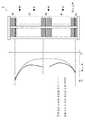
도 1은 본 발명의 제1 실시 형태에 따른 종형 열처리 장치의 종단 측면도이다.
도 2는 상기 종형 열처리 장치의 횡단 평면도이다.
도 3은 제품 웨이퍼의 종단 측면도이다.
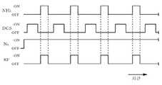
도 4는 상기 종형 열처리 장치의 처리의 타이밍 차트이다.
도 5는 제1 실시 형태에서 제품 웨이퍼에 성막되는 모습을 도시하는 설명도이다.
도 6은 비교예에서 제품 웨이퍼에 성막되는 모습을 도시하는 설명도이다.
도 7은 상기 종형 열처리 장치에서 처리된 웨이퍼 간의 막 두께 분포를 나타내는 그래프이다.
도 8은 웨이퍼 보트에서의 제품 웨이퍼의 배치 예를 도시하는 설명도이다.
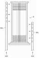
도 9는 제2 실시 형태에 따른 종형 열처리 장치의 종단 측면도이다.
도 10은 상기 종형 열처리 장치의 횡단 평면도이다.
도 11은 상기 종형 열처리 장치에서 처리된 웨이퍼 간의 막 두께 분포를 나타내는 그래프이다.
도 12는 제3 실시 형태에 따른 웨이퍼 보트를 사용하여 처리된 웨이퍼 간의 막 두께 분포를 나타내는 그래프이다.
도 13은 제4 실시 형태에 따른 웨이퍼 보트를 사용하여 처리된 웨이퍼 간의 막 두께 분포를 나타내는 그래프이다.
도 14는 평가 시험에서 사용한 인젝터의 구성을 도시하는 설명도이다.
도 15는 평가 시험의 결과를 나타내는 그래프이다.1 is a longitudinal side view of a vertical type heat treatment apparatus according to a first embodiment of the present invention.
2 is a cross-sectional plan view of the vertical heat treatment apparatus.
3 is a longitudinal side view of the product wafer.
4 is a timing chart of the processing of the above described vertical type heat treatment apparatus.
5 is an explanatory view showing a state in which a film is formed on a product wafer in the first embodiment.
6 is an explanatory view showing a state in which a film is formed on a product wafer in a comparative example.
FIG. 7 is a graph showing the film thickness distribution among the wafers processed in the vertical heat treatment apparatus.
8 is an explanatory diagram showing an example of the arrangement of a product wafer in a wafer boat.
9 is a longitudinal side view of the vertical type heat treatment apparatus according to the second embodiment.
10 is a cross-sectional plan view of the vertical heat treatment apparatus.
11 is a graph showing the film thickness distribution among the wafers processed in the vertical heat treatment apparatus.
12 is a graph showing the film thickness distribution among the wafers processed using the wafer boat according to the third embodiment.
13 is a graph showing the film thickness distribution among the wafers processed using the wafer boat according to the fourth embodiment.
14 is an explanatory diagram showing the configuration of the injector used in the evaluation test.
15 is a graph showing the results of the evaluation test.
(제1 실시 형태)(First Embodiment)
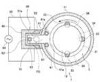
본 발명의 제1 실시 형태에 대해서 도면에 기초하여 설명한다. 도 1 및 도 2는 본 발명에 따른 종형 열처리 장치(1)의 개략 종단면도 및 개략 횡단면도이다. 도 1 및 도 2의 11은, 예를 들어 석영에 의해 종형의 원기둥 형상으로 형성된 처리 용기를 이루는 반응관이다. 또한, 이 반응관(11)의 하단 개구부의 주연부에는 플랜지(12)가 일체로 형성되어 있고, 이 플랜지(12)의 하면에는, 예를 들어 스테인레스 스틸에 의해 원통 형상으로 형성된 매니폴드(2)가 O링 등의 시일 부재(21)를 개재하여 연결되어 있다.A first embodiment of the present invention will be described with reference to the drawings. 1 and 2 are a schematic vertical sectional view and a schematic cross sectional view of a vertical type
상기 매니폴드(2)의 하단은, 반입출구(노구)로서 개구되고, 그 개구부(22)의 주연부에는 플랜지(23)가 일체로 형성되어 있다. 상기 매니폴드(2)의 하방에는, 플랜지(23)의 하면에 O링 등의 시일 부재(24)를 개재하여 개구부(22)를 기밀하게 폐색하는, 예를 들어 석영제의 덮개(25)가 보트 엘리베이터(26)에 의해 상하 방향으로 개폐 가능하게 설치되어 있다. 상기 덮개(25)의 중앙부에는 회전축(27)이 관통하여 설치되고, 그 상단부에는 스테이지(39)를 개재하여 기판 보유 지지구인 웨이퍼 보트(3)가 탑재되어 있다.The lower end of the
상기 매니폴드(2)의 측벽에는, L자형의 제1 원료 가스 공급관(40)이 삽입되어 설치되어 있고, 상기 제1 원료 가스 공급관(40)의 선단부에는, 도 2에 도시한 바와 같이 반응관(11) 내에서 상측 방향으로 연장되는 석영관으로 이루어지는 2개의 제1 원료 가스 공급 노즐(41)이, 후술하는 플라즈마 발생부(60)의 가늘고 긴 개구부(61)를 사이에 두고 배치되어 있다. 이들 제1 원료 가스 공급 노즐(41, 41)에는, 그 길이 방향을 따라 복수(다수)의 가스 토출 구멍(41a)이 소정의 간격을 두고 형성되어 있고, 각 가스 토출 구멍(41a, 41a)으로부터 수평 방향을 향해 대략 균일하게 가스를 토출할 수 있도록 되어 있다. 또한, 상기 제1 원료 가스 공급관(40)의 기단 측에는, 공급 기기 군(42)을 개재하여 제1 원료 가스인 실란계의 가스, 예를 들어 SiH2Cl2(디클로로실란: DCS) 가스의 공급원(43)이 접속되어 있다.2, an L-shaped first source
또한, 상기 매니폴드(2)의 측벽에는, L자형의 제2 원료 가스 공급관(50)이 삽입되어 설치되어 있고, 상기 제2 원료 가스 공급관(50)의 선단부에는, 반응관(11) 내에서 상측 방향으로 연장되고 도중에 굴곡되어, 후술하는 플라즈마 발생부(60) 내에 설치되는 석영으로 이루어지는 제2 원료 가스 공급 노즐(51)이 설치되어 있다. 이 제2 원료 가스 공급 노즐(51)에는, 그 길이 방향을 따라 복수(다수)의 가스 토출 구멍(51a)이 소정의 간격을 두고 형성되어 있고, 각 가스 토출 구멍(51a)으로부터 수평 방향을 향해 대략 균일하게 가스를 토출할 수 있도록 되어 있다. 또한, 상기 제2 원료 가스 공급관(50)의 기단측은 2개로 분기되어 있어, 한쪽의 제2 원료 가스 공급관(50)에는 공급 기기 군(52)을 개재하여 제2 원료 가스인 암모니아(NH3) 가스의 공급원(53)이 접속되어 있고, 다른 쪽의 제2 원료 가스 공급관(50)에는 공급 기기 군(54)을 개재하여 질소(N2) 가스의 공급원(55)이 접속되어 있다.An L-shaped second raw material
또한, 매니폴드(2)의 측벽에는, 클리닝 가스 공급관(45)의 일단이 삽입되어 설치되어 있다. 클리닝 가스 공급관(45)의 타단은 분기되어, 각각 공급 기기 군(46, 47)을 개재하여, F2(불소) 가스의 가스 공급원(48), HF(불화수소)의 가스 공급원(49)에 각각 접속되어 있다. 이에 의해, 반응관(11) 내에 클리닝 가스로서, F2와 HF의 혼합 가스를 공급할 수 있다. 클리닝 가스로서는 이러한 불소 가스 또는 불화수소 가스를 주성분으로 하는 가스를 사용하는 것에 한정되지 않고, 예를 들어 다른 불소 화합물을 주성분으로 하는 가스를 사용해도 된다. 또한, 상기 공급 기기 군(42, 46, 47, 52, 54)의 각각은, 밸브 및 유량 조정부 등에 의해 구성되어 있다.One end of a cleaning
또한, 상기 반응관(11)의 측벽의 일부에는, 그 높이 방향을 따라서 플라즈마 발생부(60)가 설치되어 있다. 상기 플라즈마 발생부(60)는, 상기 반응관(11)의 측벽을 상하 방향을 따라서 소정의 폭으로 깎아냄으로써 상하로 가늘고 긴 개구부(61)를 형성하고, 이 개구부(61)를 덮도록, 단면 오목부 형상으로 이루어진 상하로 가늘고 긴, 예를 들어 석영제의 구획벽(62)을 반응관(11)의 외벽에 기밀하게 용접 접합함으로써 구성된다. 이 구획벽(62)에 의해 둘러싸이는 영역이 플라즈마 발생 영역(PS)이 된다.A part of the side wall of the
상기 개구부(61)는, 웨이퍼 보트(3)에 보유 지지되어 있는 모든 웨이퍼를 높이 방향에서 커버할 수 있도록 상하 방향으로 충분히 길게 형성되어 있다. 또한, 상기 구획벽(62)의 양 측벽의 외측면에는, 그 길이 방향(상하 방향)을 따라 서로 대향하도록 가늘고 긴 한 쌍의 플라즈마 전극(63)이 설치되어 있다. 이 플라즈마 전극(63)에는, 플라즈마 발생용의 고주파 전원(64)이 급전 라인(65)을 통하여 접속되어 있고, 상기 플라즈마 전극(63)에, 예를 들어 13.56MHz의 고주파 전압을 인가함으로써 플라즈마를 발생할 수 있게 되어 있다. 또한, 상기 구획벽(62)의 외측에는, 상기 구획벽(62)을 덮도록, 예를 들어 석영으로 이루어지는 절연 보호 커버(66)가 설치되어 있다.The
또한, 매니폴드(2)에는, 반응관(11) 내의 분위기를 진공 배기하기 위하여 배기구(67)가 개구되어 있다. 배기구(67)에는, 반응관(11) 내를 원하는 진공도로 감압 배기 가능한 진공 배기 수단을 이루는 진공 펌프(68) 및 예를 들어 버터플라이 밸브로 이루어지는 압력 조정부(69)를 구비한 배기관(59)이 접속되어 있다. 또한, 도 1에 도시한 바와 같이 반응관(11)의 외주를 둘러싸도록 하여, 반응관(11) 및 반응관(11) 내의 웨이퍼를 가열하는 가열 수단인 통 형상체의 히터(28)가 설치되어 있다.An
또한, 상기의 종형 열처리 장치(1)는 제어부(100)를 구비하고 있다. 상기 제어부(100)는, 예를 들어 컴퓨터로 이루어지고, 보트 엘리베이터(26), 히터(28), 공급 기기 군(42, 46, 47, 52, 54), 고주파 전원(64), 압력 조정부(69) 등을 제어하도록 구성되어 있다. 보다 구체적으로는, 제어부(100)는, 반응관(11) 내에서 행하여지는 후술하는 일련의 처리 스텝을 실행하기 위한 시퀀스 프로그램을 기억하는 기억부, 각 프로그램의 명령을 판독하여 각 부에 제어 신호를 출력하는 수단 등을 구비하고 있다. 또한, 이 프로그램은, 예를 들어 하드 디스크, 플렉시블 디스크, 콤팩트 디스크, 마그네트 옵티컬 디스크(MO), 메모리 카드 등의 기억 매체에 저장된 상태로 제어부(100)에 저장된다.The above-described vertical type
계속해서, 상기 웨이퍼 보트(3)에 대하여 더 설명한다. 웨이퍼 보트(3)는 석영으로 이루어지고, 성막 처리 시에 서로 평행하게 놓이는 천장판(31)과 저판(32)을 구비하고, 이들 천장판(31) 및 저판(32)은, 상하로 연장되는 3개의 지주(33)의 일단 및 타단에 각각 접속되어 있다. 각 지주(33)에는, 다단으로 지지부(34)(도 2 참조)가 설치되고, 이 지지부(34) 위에 웨이퍼를 수평하게 유지할 수 있도록 구성되어 있다. 따라서, 웨이퍼 보트(3)에 웨이퍼는, 다단으로 선반 형상으로 유지된다. 각 지지부(34) 위에서의 웨이퍼가 지지되는 영역을 슬롯이라 표기하고, 이 예에서는 슬롯이 120개 설치된다. 또한, 각 슬롯은 1 내지 120의 번호로 표현되고, 상단측의 슬롯일수록 작은 번호가 붙여져 있다.Next, the
이 제1 실시 형태에서는, 상기 슬롯에 웨이퍼(10)와 웨이퍼(71)가 탑재된다. 웨이퍼(10)는, 배경기술의 항목에서 설명한 반도체 제품을 제조하기 위한 제품 웨이퍼이며, 예를 들어 실리콘 기판에 의해 구성되어 있다. 도 3에 도시한 바와 같이, 웨이퍼(10)의 표면에는 배선을 형성하기 위한 요철이 형성되어 있다. 도면 중, 35는 폴리실리콘막, 36은 텅스텐막이다. 37은, 이들 막(35, 36)에 형성된 오목부이다. 38은, 이 종형 열처리 장치(1)에 의해 성막되는 SiN막(실리콘 질화막)이다.In the first embodiment, the
웨이퍼(71)는, 석영에 의해 구성되는 웨이퍼(이하, 석영 웨이퍼라고 기재함)이다. 석영 웨이퍼(71)는, 웨이퍼 보트(3)에 적재할 수 있도록 평면에서 보아 그 외형이, 웨이퍼(10)의 외형에 일치하도록 구성된다. 취급 시의 파손을 방지하기 위해서, 석영 웨이퍼(71)의 두께는, 예를 들어 웨이퍼(10)의 두께보다 약간 크며, 예를 들어 2mm로 구성된다. 도 1의 점선의 화살표 끝에 나타내는 점선의 원 내에는, 석영 웨이퍼(71)의 종단 측면을 확대하여 나타내고 있다. 여기에 도시된 바와 같이, 석영 웨이퍼(71)의 표면 및 이면에는 요철이 형성되어 있다. 이 요철은 예를 들어 레이저 가공이나 기계 가공 등에 의해 형성된다.The
웨이퍼(10)의 표면적을, 웨이퍼(10)의 외형 치수에 기초하여 계산되는 표면적으로 나눔으로써 얻어지는 단위 영역당의 표면적을 S0으로 한다. 상기 외형 치수로 구해지는 표면적이란, 웨이퍼(10)의 표면의 오목부(37)를 고려하지 않고, 웨이퍼(10)의 표면이 평탄면인 것으로 해서 구해지는 가상의 표면적이다. 즉, 실제의 웨이퍼(10)의 표면적을 상기 가상의 표면적으로 나눈 값이, 상기 단위 영역당의 표면적(S0)이다. 여기에서 말하는 웨이퍼의 표면적이란, 웨이퍼의 상면(표면)의 면적+하면(이면)의 면적으로 한다. 그리고, 석영 웨이퍼(71)의 표면적을, 당해 석영 웨이퍼(71)의 외형 치수에 기초하여 계산되는 표면적으로 나눔으로써 얻어지는 단위 영역당의 표면적을 S로 한다. 석영 웨이퍼(71)에 관한 상기 외형 치수로 구해지는 표면적이란, 웨이퍼(10)의 경우와 마찬가지로, 석영 웨이퍼(71)의 표면 및 이면에 형성된 오목부를 고려하지 않고, 석영 웨이퍼(71)의 표면 및 이면이 평탄면인 것으로 해서 구해지는 가상의 표면적이다. 후술하는 바와 같이 웨이퍼 보트(3)의 상하 방향에서의 가스 분포를 조정하기 위해, S/S0은 0.8 이상이 되도록 설정된다. 이 예에서는 S/S0=1이 되도록 석영 웨이퍼(71)가 구성되어 있다.Let S0 be the surface area per unit area obtained by dividing the surface area of the
도 1에 도시한 바와 같이 석영 웨이퍼(71)는, 웨이퍼 보트(3)의 슬롯 중, 상단측 및 하단측의 복수의 슬롯에 보유 지지된다. 석영 웨이퍼(71)가 유지되어 있지 않은 슬롯에는, 웨이퍼(10)가 유지된다. 따라서, 석영 웨이퍼(71)에 상하로부터 끼워지도록, 웨이퍼(10) 군이 웨이퍼 보트(3)에 유지된다. 상기 석영 웨이퍼(71)는, 웨이퍼(10)와 마찬가지로 웨이퍼 보트(3)에 대하여 착탈 가능하게 구성해도 되고, 고정되어 있어도 된다. 웨이퍼(10)는, 웨이퍼 보트(3)에 대하여 도시하지 않은 이동 탑재 기구에 의해 이동 탑재된다. 석영 웨이퍼(71)를 웨이퍼 보트(3)에 대하여 착탈 가능하게 구성하는 경우에는, 예를 들어 이 이동 탑재 기구에 의해 웨이퍼(10)와 마찬가지로 이동 탑재된다. 취급이 용이한 점에서, 이 예에서는 석영 웨이퍼(71)는 웨이퍼 보트(3)에 고정되어 있는 것으로 한다.As shown in Fig. 1, the
계속해서, 종형 열처리 장치(1)에서 실시되는 성막 처리에 대하여 설명한다. 우선, 상기와 같이 석영 웨이퍼(71)에 상하로 끼워지도록 웨이퍼(10) 군을 적재한 웨이퍼 보트(3)를 미리 소정의 온도로 설정된 반응관(11) 내에, 그 하방으로부터 상승시켜서 반입(로드)하고, 덮개(25)로 매니폴드(2)의 하단 개구부(22)를 폐쇄함으로써 반응관(11) 내를 밀폐한다.Subsequently, the film forming process performed in the vertical
그리고, 반응관(11) 내를 진공 펌프(68)에 의해 진공화하여, 반응관(11) 내가 소정의 진공도가 되도록 한다. 계속해서 반응관(11) 내의 압력을 예를 들어 665.5Pa(5Torr)로 하고, 제1 원료 가스 공급 노즐(41)로부터 반응관(11) 내에 DCS 가스 및 N2 가스를 각각 예를 들어 1000sccm, 2000sccm의 유량으로, 예를 들어 3초간, 고주파 전원(64)이 오프인 상태에서 공급하여, 회전하고 있는 웨이퍼 보트(3)에 선반 형상으로 보유 지지되어 있는 웨이퍼(10)의 표면에 DCS 가스의 분자를 흡착시킨다(스텝 S1).Then, the inside of the
그 후, DCS 가스의 공급을 멈추고, 반응관(11) 내에는 N2 가스를 계속해서 공급함과 함께 반응관(11) 내의 압력을 예를 들어 120Pa(0.9Torr)로 해서, 반응관(11) 내를 N2 퍼지한다(스텝 S2). 계속해서, 반응관(11) 내의 압력을 예를 들어 54Pa(0.4Torr)로 하고, 제2 원료 가스 공급 노즐(51)로부터 반응관(11) 내에 NH3 가스 및 N2 가스를 각각 예를 들어 5000sccm, 2000sccm의 유량으로, 예를 들어 20초간, 고주파 전원(64)이 온인 상태에서 공급한다(스텝 S3). 이에 의해 N 라디칼, H 라디칼, NH 라디칼, NH2 라디칼, NH3 라디칼 등의 활성종과 DCS 가스의 분자가 반응하여, 도 3에 도시한 SiN막(38)이 생성된다.Thereafter, the supply of the DCS gas is stopped and N2 gas is continuously supplied into the
그런 뒤, NH3 가스의 공급을 멈추고, 반응관(11) 내에는 N2 가스를 계속해서 공급함과 함께 반응관(11) 내의 압력을 예를 들어 106Pa(0.8Torr)로 하여 반응관(11) 내를 N2 퍼지한다(스텝 S4). 도 4는 각 가스의 공급 타이밍과 고주파 전원(64)을 온으로 하는 타이밍을 나타낸 타이밍 차트이다. 이 차트에 나타낸 바와 같이, 상기 스텝 S1 내지 스텝 S4를 복수 회 예를 들어 200회 반복함으로써, 웨이퍼(10)의 표면에 SiN막(38)의 박막이, 소위 1층씩 적층되어 성장하여, 웨이퍼(10)의 표면에 원하는 두께의 SiN막(38)이 형성된다.Thereafter, the supply of the NH3 gas is stopped and the N2 gas is continuously supplied into the
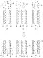
도 5의 모식도를 사용하여, 상기의 성막 처리 중에 DCS 가스가 공급되었을 때의, 웨이퍼(10) 및 석영 웨이퍼(71)의 상태를 설명한다. 도면 중 70은 DCS 가스의 분자이다. 웨이퍼 보트(3)의 중단에서는, 그 표면에 요철이 형성됨으로써 표면적이 큰 웨이퍼(10)가 다단으로 배치되어 있고, 웨이퍼 보트(3)의 중단에 공급된 상기 분자(70)는, 이 웨이퍼(10)에 소비(흡착)된다. 이렇게 분자(70)가, 웨이퍼(10) 사이에서 균일성 높게 분배되도록 소비되어, 웨이퍼(10)의 1장당의 분자(70)의 흡착량이 과잉이 되는 것이 억제된다.The state of the
그리고, 웨이퍼 보트(3)의 상단 및 하단에 보유 지지된 웨이퍼(10)에 대해서도, 중단에 보유 지지된 웨이퍼(10)와 마찬가지로, 그 근방에 표면적이 크게 구성된 웨이퍼, 즉 석영 웨이퍼(71)가 존재한다. 따라서, 웨이퍼 보트(3)의 상단 및 하단에 공급된 상기 분자(70)가, 웨이퍼(10) 및 석영 웨이퍼(71)에 있어서 균일성 높게 분배되도록 소비된다. 즉, 그 표면적이 크기 때문에 석영 웨이퍼(71)에서의 분자(70)의 흡착량이 비교적 많으므로, 과잉의 분자(70)가 웨이퍼(10)에 공급되는 것이 억제되어, 웨이퍼(10)의 1장당의 분자(70)의 흡착량이 과잉이 되는 것이 억제된다.As for the
도 5와의 비교를 위해서, 도 6의 모식도를 나타내고 있다. 도 6은, 앞서 서술한 석영 웨이퍼(71)가 배치되는 각 슬롯에, 당해 석영 웨이퍼(71) 대신에 배경기술의 항목에서 설명한 베어 웨이퍼(72)를 배치하여 처리를 행한 경우에 있어서, 웨이퍼(10)에 분자(70)가 흡착되는 모습을 나타내고 있다. 이미 설명한 바와 같이 베어 웨이퍼(72)는, 예를 들어 실리콘에 의해 구성되고, 그 표면에 디바이스 형성용의 요철이 형성되어 있지 않기 때문에 표면적이 작다. 당해 베어 웨이퍼(72)를 배치한 경우에도, 웨이퍼 보트(3)의 중단에서는, 도 5에서 설명한 바와 같이 각 웨이퍼(10)에 분자(70)가 분배되어서 1장당의 웨이퍼(10)에 대한 흡착량이 억제된다. 그러나, 웨이퍼 보트(3)의 상단 및 하단에 보유 지지된 웨이퍼(10)에 대해서는, 그 근방에 베어 웨이퍼(72)가 존재하고, 당해 베어 웨이퍼(72)는, 그 표면적이 작기 때문에 분자(70)의 흡착량이 작으므로, 베어 웨이퍼(72)에서 전부 소비하지 못한 잉여의 분자(70)가 당해 웨이퍼(10)에 흡착되어버린다.For comparison with Fig. 5, a schematic diagram of Fig. 6 is shown. 6 shows a case in which the
도 5 및 도 6에서 설명한 바와 같이, 석영 웨이퍼(71)를 웨이퍼 보트(3)에 보유 지지함으로써, 웨이퍼 보트의 상단측 및 하단측의 웨이퍼(10)에 과잉으로 분자(70)가 흡착되는 것을 억제하고, 결과적으로 웨이퍼 간에 균일성 높게 분자(70)가 흡착된다. DCS 가스의 분자(70)가 흡착되는 예에 대하여 설명했지만, 석영 웨이퍼(71)를 웨이퍼 보트(3)에 보유 지지함으로써, 상기의 NH3 가스, N2 가스로부터 발생한 라디칼도 각 웨이퍼(10) 사이에, 상기 분자(70)와 마찬가지로 균일성 높게 공급된다. 그리고, 공급된 라디칼은 당해 분자(70)와 반응한다.5 and 6, by retaining the
상기와 같이 스텝 S1 내지 S4를 200회 반복하여 프로세스를 종료한 후, 웨이퍼 보트(3)가 반응관(11)으로부터 반출된다. 처리를 종료한 웨이퍼(10)가 웨이퍼 보트(3)로부터 취출된 후, 당해 웨이퍼 보트(3)가 다시 반응관(11)에 반입되고, 상기 개구부(22)가 폐쇄된다. 반응관(11) 내를 진공화하여 소정의 압력으로 설정함과 함께, 그 온도를 예를 들어 350℃로 설정한다. 그리고, 앞서 서술한 F2 및 HF로 이루어지는 클리닝 가스를, 반응관(11) 내에 공급한다. 이에 의해, 반응관(11) 내, 웨이퍼 보트(3) 및 석영 웨이퍼(71)에 성막된 SiN막(38)이 에칭되어, 배기류를 타고 반응관(11)으로부터 제거된다. 그러한 후, 클리닝 가스의 공급을 정지하고, 웨이퍼 보트(3)가 반응관(11)으로부터 반출된다. 그 후, 웨이퍼 보트(3)에는 후속의 웨이퍼(10)가 탑재되어, 상기의 스텝 S1 내지 S4에 따라서 당해 후속의 웨이퍼(10)에 성막 처리가 행하여진다.After the steps S1 to S4 are repeated 200 times as described above, the
도 7에는, 웨이퍼(10)의 막 두께와 슬롯의 위치의 관계를 나타낸 그래프를 나타내고 있다. 그래프의 횡축은 웨이퍼(10)의 막 두께에 대응하고, 종축은 슬롯의 위치에 대응한다. 그래프의 종축과 그 높이가 대응하도록 웨이퍼 보트(3)를, 슬롯 번호를 붙여서 나타내고 있다. 점선으로 나타내는 그래프는 실험에 기초하여 취득된 데이터이며, 도 6에서 설명한 바와 같이 석영 웨이퍼(71) 대신에 베어 웨이퍼(72)를 웨이퍼 보트(3)에 보유 지지하여 성막 처리를 행한 경우에 있어서의 각 슬롯의 웨이퍼(10)의 막 두께 분포를 나타내고 있다. 도 6에서 앞서 서술한 이유에 의해, 보트(3)의 중단의 슬롯으로부터, 상단 및 하단의 슬롯을 향함에 따라서 점차로 웨이퍼(10)의 막 두께는 커지고 있어, 상단부 및 하단부에서의 슬롯의 웨이퍼(10)와, 중단부에서의 슬롯의 웨이퍼(10)에서 막 두께의 차가 비교적 크다. 즉, 슬롯 간에 막 두께의 편차가 크다. 또한, 도 7 중의 웨이퍼 보트(3)에는, 이 베어 웨이퍼(72)가 아니라, 실시 형태에 따라서 석영 웨이퍼(71)를 보유 지지한 상태를 나타내고 있다.7 is a graph showing the relationship between the film thickness of the
도 7의 실선 그래프는, 도 1 내지 도 5에서 설명한 바와 같이, 석영 웨이퍼(71)를 배치하여 처리를 행하는 경우에 상정되는 그래프이며, 제1 실시 형태의 효과를 나타낸다. 도 5에서 설명한 이유에 의해, 석영 웨이퍼(71)에 의해 웨이퍼 보트(3)의 상부측 및 하부측의 웨이퍼(10)에 대한 과잉의 가스의 공급이 억제되므로, 그래프에 표시하는 바와 같이, 이들 상부측 및 하부측의 웨이퍼(10)의 막 두께가 커지는 것이 억제된다. 결과적으로, 각 슬롯 간에 웨이퍼(10)의 막 두께의 균일성을 높게 할 수 있다.The solid line graph of Fig. 7 is a graph assumed when the
또한, 석영 웨이퍼(71)의 표면적을 크게 할수록, 웨이퍼 보트(3)의 상부측 및 하부측의 웨이퍼(10)에 대한 가스의 공급을 억제할 수 있다고 생각된다. 도 7 중의 이점 쇄선의 그래프는, 석영 웨이퍼(71)의 표면적을 웨이퍼(10)의 표면적보다 크게 한 경우에 상정되는 막 두께 분포의 그래프이다. 웨이퍼(10)의 표면적에 따라, 적절한 막 두께 분포가 되도록 석영 웨이퍼(71)의 표면적이 결정된다. 또한, 석영 웨이퍼(71)는, 웨이퍼 보트(3)의 상부, 하부에 각각 1매만 설치해도, 이미 설명한 바와 같이 웨이퍼(10)의 가스 분포를 조정할 수 있다. 그러나, 웨이퍼(10) 사이의 온도 분포를 제어하는 관점에서, 복수 매 설치하는 것이 바람직하다.It is considered that the supply of gas to the
또한, 석영 웨이퍼(71)는 석영이기 때문에, Si로 이루어지는 웨이퍼에 비하여, 상기의 불소 가스 또는 불소 화합물로 이루어지는 가스인 클리닝 가스에 의한 부식이 억제된다. 이 때문에, 상기한 바와 같이 상기 성막 처리에 반복해서 사용할 수 있다. 또한, 클리닝을 행하기 위해 습식 에칭을 행하는 장치에 반송할 필요가 없으므로, 장치 운용의 수고가 억제된다.Further, since the
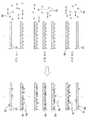
그런데 웨이퍼 보트(3)에 비교적 적은 매수의 웨이퍼(10)를 보유 지지하여 처리를 행하는 경우가 있다. 그 경우, 예를 들어 도 8에 도시한 바와 같이 웨이퍼(10)를 보유 지지하여 처리를 행한다. 설명하자면, 웨이퍼(10)를 중단의 슬롯에 보유 지지한다. 도 8의 예에서는, 번호가 35 부근 내지 60 부근의 슬롯에 연속해서 웨이퍼(10)를 적재하고 있다. 그리고, 그 상하의 슬롯에 상기 석영 웨이퍼(71)를 각각 예를 들어 복수 매 보유 지지한다. 도 8에 나타내는 예에서는, 웨이퍼(10)가 보유 지지되는 슬롯의 상하에 각각 5장 정도의 석영 웨이퍼(71)가 보유 지지되어 있다.However, a relatively small number of
이 석영 웨이퍼(71)군 및 웨이퍼(10) 군을 사이에 끼워넣도록, 웨이퍼 보트(3)의 상측의 각 슬롯 및 하측의 각 슬롯에는, 상기 베어 웨이퍼(72)가 보유 지지된다. 이 베어 웨이퍼(72)는, 반응관(11) 내에서의 가스의 흐름의 혼란이나, 웨이퍼(10)에서의 온도 분포의 혼란을 방지하기 위해 탑재되어 있다. 이렇게 1번 내지 120번의 슬롯에는, 웨이퍼(10), 석영 웨이퍼(71) 및 베어 웨이퍼(72) 중 어느 하나가 보유 지지된다.The
도 8에는, 도 7과 마찬가지로 막 두께 분포를 나타내는 그래프도 표시하고 있다. 실선의 그래프는, 상기와 같이 웨이퍼 보트(3)에 석영 웨이퍼(71)를 탑재하여 웨이퍼(10)에 처리를 행한 경우에 상정되는 웨이퍼(10)의 막 두께 분포를 나타낸다. 점선의 그래프는, 상기의 설명에서 석영 웨이퍼(71)가 보유 지지된 슬롯에 대해서, 석영 웨이퍼(71) 대신에 베어 웨이퍼(72)를 보유 지지하여 처리를 행한 경우에 있어서의 웨이퍼(10)의 막 두께 분포를 나타낸다. 이 도 8의 그래프에 예시한 바와 같이, 소수 매의 웨이퍼(10)에 대하여 처리를 행하는 경우도 석영 웨이퍼(71)를 상기와 같이 웨이퍼 보트(3)에 탑재함으로써, 도 5 및 도 6에서 설명한 이유에 의해, 웨이퍼 보트(3)에 탑재된 웨이퍼(10)군 중, 상방측의 웨이퍼(10) 및 하방측의 웨이퍼(10)의 막 두께가 커지는 것을 방지할 수 있다. 그 결과, 웨이퍼(10) 간의 막 두께의 균일성을 높게 할 수 있다.Fig. 8 also shows a graph showing the film thickness distribution as in Fig. The solid line graph shows the film thickness distribution of the
(제2 실시 형태)(Second Embodiment)
도 5에서 설명한 바와 같이, 웨이퍼 보트(3)에 탑재된 웨이퍼(10) 군보다 상방 및 하방에 비교적 표면적이 큰 부재가 있으면, 웨이퍼(10) 군에 있어서 상방측, 하방측의 가스 공급량을 저하시켜서, 웨이퍼(10) 간에 막 두께 분포를 조정할 수 있다. 따라서, 이러한 가스 분포를 조정하는 조정 부재로서는, 석영 웨이퍼(71)인 것에 한정되지 않는다. 도 9 및 도 10은, 제2 실시 형태에 따른 종형 열처리 장치(1)의 종단 측면도 및 횡단 평면도를 각각 나타내고 있다. 제2 실시 형태의 종형 열처리 장치(1)는, 제1 실시 형태와는 반응관(11)의 구성이 상이하고, 다른 각 부에 대해서는 마찬가지로 구성되어 있다. 도 9 및 도 10에서는, 제1 실시 형태에서 설명한 부재의 일부를 생략하고 있다.5, if there is a member having a relatively large surface area above and below the group of
이 제2 실시 형태의 종형 열처리 장치(1)에서는, 반응관(11)의 천장면과 상부측 둘레면을 포함하는 상방 영역(81), 반응관(11)의 하방측 둘레면인 하방 영역(82)에 대해서, 그 표면적을 크게 하기 위해 요철이 형성되어 있다. 이들 상방 영역(81) 및 하방 영역(82)은 반응관(11)의 내주면이다. 상기 하방 영역(82)은, 반응관(11)에 웨이퍼 보트(3)가 수납되었을 때에, 웨이퍼 보트(3)에 적재된 웨이퍼(10) 군보다 하방의 영역을 포함하고 있다. 상방 영역(81) 및 하방 영역(82)의 요철은, 예를 들어 샌드블라스트나 약액 처리에 의해 형성되어 있다. 샌드블라스트로 처리한 경우, 산술 평균 조도(Ra)는 예를 들어 0.4 내지 4.0㎛이며, 약액 처리한 경우, 산술 평균 조도(Ra)는 0.3 내지 4.0㎛이다. 제1 실시 형태의 석영 웨이퍼(71)에서도, 이러한 샌드블라스트나 약액 처리에 의해 요철의 형성을 행해도 된다. 또한, 석영 웨이퍼(71)와 동일하게, 레이저 가공에 의해 반응관(11)에 당해 요철을 형성해도 된다.In the vertical
이렇게 거칠음(요철)이 형성됨으로써, 상기 상방 영역(81) 및 하방 영역(82)은, 제1 실시 형태의 석영 웨이퍼(71)와 마찬가지로 가스의 공급 분포를 조정하는 역할을 한다. 이를 위해, 상방 영역(81) 및 하방 영역(82)에 대해서, 각각의 단위 영역당의 표면적을 S로 하면, 웨이퍼(10)의 단위 영역당의 표면적(S0)과의 관계는, 제1 실시 형태와 마찬가지로 S/S0이 0.8 이상이 되도록 상기 요철이 형성된다. 이 상방 영역(81) 및 하방 영역(82)의 표면적이란, 가스가 공급되는 처리 공간에 면하는 면의 표면적이다. 일례로서 상방 영역(81)의 단위 영역당의 표면적(S)에 대해서 더욱 구체적으로 설명하기 위해, 상방 영역(81)에 대해서, 상기 요철이 없는 것으로 하여 웨이퍼(10)의 외형에 둘러싸이는 영역의 면적과 동일한 면적(A)을 갖도록 잘라냈다고 가정한다. 이 잘라낸 부위에 대해서, 반응관(11) 내의 처리 공간에 면하는 면의 표면적을 B로 하면, 상기 S는 B/A이다. 상기 표면적(B)은, 요철이 있는 것으로 하여 측정되는 표면적이다. 하방 영역(82)의 S도 마찬가지로 계산된다.By forming such roughness (concavity and convexity), the
반응관(11)의 내주측면에 있어서, 상기 상방 영역(81)과 하방 영역(82) 사이에 끼워지는 영역을 중간 영역(83)으로 한다. 이 중간 영역(83)은, 반응관(11)에 웨이퍼 보트(3)가 반입되었을 때에 웨이퍼(10) 군의 외주에 위치한다. 중간 영역(83)에는, 상기 샌드블라스트 및 약액 처리가 행하여지지 않고, 평활면으로서 구성되어 있다. 즉, 상방 영역(81), 하방 영역(82)에 비해, 중간 영역(83)의 거칠음은 작다.An area sandwiched between the
이 제2 실시 형태의 종형 열처리 장치(1)에서도, 제1 실시 형태와 마찬가지로 성막 처리 및 클리닝 처리가 행하여진다. 상기와 같이 반응관(11)의 내주면이 거칠어지게 구성됨으로써, 성막 처리 시에 웨이퍼 보트(3)의 상부측 및 하부측에 공급된 가스가 상기 상방 영역(81) 및 하방 영역(82)에서 소비된다. 그에 의해, 제1 실시 형태와 마찬가지로, 웨이퍼 보트(3)의 상부측 및 하부측에 보유 지지된 웨이퍼(10)에 과잉으로 가스가 공급되는 것을 방지할 수 있다. 이렇게 반응관(11)의 상방 영역(81) 및 하방 영역(82)이 제1 실시 형태의 석영 웨이퍼(71)와 마찬가지의 역할을 하기 때문에, 이 예에서는 웨이퍼 보트(3)에는 제1 실시 형태와 달리, 석영 웨이퍼(71) 대신에 베어 웨이퍼(72)가 웨이퍼 보트(3)에 대하여 착탈 가능하게 보유 지지되어 있다. 즉, 베어 웨이퍼(72)에 상하가 끼워지도록 웨이퍼(10) 군이 보유 지지되어 있다. 클리닝 처리 시에는, 베어 웨이퍼(72)는, 석영 웨이퍼(71)를 사용하는 경우와 달리, 보트(3)로부터 제거해 둔다.In the vertical type
도 11은, 도 7과 마찬가지로 각 슬롯의 웨이퍼(10)의 막 두께 분포를 나타낸다. 도면 중의 점선 그래프는, 반응관(11)에 상기의 거칠음을 형성하지 않고 처리를 행한 경우의 웨이퍼(10)의 막 두께 분포를 나타내고 있다. 도면 중의 실선 그래프는, 상기와 같이 상방 영역(81) 및 하방 영역(82)에 거칠음을 형성하여 처리를 행한 경우에, 상정되는 웨이퍼(10) 간의 막 두께 분포이다. 그래프에서 예시한 바와 같이, 반응관(11) 내에 상기 거칠음을 형성함으로써, 제1 실시 형태와 마찬가지로 보트(3)에 보유 지지되는 웨이퍼(10)군 중, 상부측의 웨이퍼(10)와, 하부측의 웨이퍼(10)에 과잉으로 가스가 공급되는 것을 방지하여, 웨이퍼(10) 간에 막 두께의 균일성을 높게 할 수 있다.11 shows the film thickness distribution of the
이 반응관(11)의 웨이퍼(10) 군보다 상부측에 있어서 거칠음을 형성하는 영역은, 천장면 및 측 둘레면 중 어느 한쪽만이어도 된다. 또한, 반응관(11)에 있어서 웨이퍼(10) 군보다 하방의 영역에 대해서는, 측 둘레면에 거칠음을 형성하는 것에 한정되지 않고, 반응관(11)의 저판, 즉 덮개(25)의 표면에 거칠음을 형성해도 된다.The area of the
(제3 실시 형태)(Third Embodiment)
제3 실시 형태에서는, 제1 실시 형태와 마찬가지의 종형 열처리 장치(1)가 사용되고, 예를 들어 반응관(11)의 내면에는 제2 실시 형태에서 설명한 거칠음이 형성되지 않는다. 그 대신에, 웨이퍼 보트(3)의 천장판(31) 및 저판(32)의 표면이, 제2 실시 형태에서 설명한 반응관(11)의 상방 영역(81) 및 하방 영역(82)과 마찬가지로 거칠어져, 그 단위 영역당의 표면적(S)/웨이퍼(10)의 단위 영역당의 표면적(S0)≥0.8이 된다. 도 12는, 이와 같이 거칠음이 형성된 웨이퍼 보트(3)를 나타내고 있다. 웨이퍼 보트(3)에는, 예를 들어 제2 실시 형태와 마찬가지로, 웨이퍼(10)와 베어 웨이퍼(72)가 탑재되어서 성막 처리가 행하여진다. 성막 처리 중에 있어서는, 상기 천장판(31) 및 저판(32)이, 제1 실시 형태에서 설명한 석영 웨이퍼(71)와, 제2 실시 형태에서 설명한 상기 반응관(11)의 상방 영역(81) 및 하방 영역(82)과 마찬가지의 역할을 하여, 웨이퍼(10) 간의 막 두께 분포가 조정된다.In the third embodiment, the vertical
웨이퍼 보트(3)의 천장판(31)의 단위 영역당의 표면적(S)에 대해서, 구체적으로 설명하기 위해, 천장판(31)에 대해서, 상기 요철이 없는 것으로 하여 웨이퍼(10)의 외형에 둘러싸이는 영역의 면적과 동일한 면적(A)을 갖도록 잘라냈다고 가정한다. 이 잘라낸 부위에 대해서, 반응관(11) 내의 처리 공간에 면하는 면의 표면적을 B로 하면, 상기 S는 B/A이다. 천장판(31)은, 상면, 하면 모두에 상기 처리 공간에 면하기 때문에, 상기 표면적(B)은, 당해 상면 및 하면의 표면적의 합계이다. 보트(3)의 저판(32)의 단위 영역당의 표면적(S)에 대해서도 마찬가지로 계산되는데, 저판(32)의 하면은, 웨이퍼 보트(3)를 지지하는 스테이지(39)(도 1 참조)에 덮여, 처리 공간에 면하고 있지 않으므로, 상기 표면적(B)은 상면의 표면적이 된다.The surface area S per unit area of the
도 12의 그래프는, 다른 도면의 그래프와 마찬가지로 웨이퍼(10)의 슬롯과 막 두께의 관계를 나타내고 있다. 점선의 그래프가 상기의 천장판(31) 및 저판(32)에 거칠음을 형성하지 않고 처리를 행한 경우의 웨이퍼(10) 간의 막 두께 분포이다. 실선의 그래프가 상기 거칠음을 형성한 웨이퍼 보트(3)에서 처리를 행했을 때에 상정되는 웨이퍼(10) 간의 막 두께 분포이다.The graph of Fig. 12 shows the relationship between the slot of the
(제4 실시 형태)(Fourth Embodiment)
제4 실시 형태에서는, 제1 실시 형태와 동일한 종형 열처리 장치(1)가 사용되고, 웨이퍼 보트(3)도 제1 실시 형태와 마찬가지로 구성된다. 제4 실시 형태에서, 웨이퍼 보트(3)에는, 웨이퍼(10) 및 베어 웨이퍼(76)가 보유 지지된다. 베어 웨이퍼(76)는, 형상은 베어 웨이퍼(72)와 마찬가지로 구성되어 있지만, Si가 아니라 석영에 의해 구성되어 있다. 제1 실시 형태와 마찬가지로 베어 웨이퍼(76)에 대하여 단위 영역당의 표면적(S)을 구했을 경우, 웨이퍼(10)의 단위 영역당의 표면적(S0)과의 관계는, S/S0<1.0이 된다.In the fourth embodiment, the same vertical type
도 13에 도시한 바와 같이, 이들 웨이퍼(10, 76)가 탑재되는 슬롯이, 제2 및 제3 실시 형태와 상이하다. 베어 웨이퍼(76)는, 제2 및 제3 실시 형태와 마찬가지로, 웨이퍼 보트(3)의 상단의 복수의 슬롯 및 하단의 복수의 슬롯에 탑재되는 것 외에, 웨이퍼 보트(3)의 중단에 있어서 번호가 연속되는 슬롯에 탑재된다. 도 13의 예에서는 50번의 슬롯부터 60번 부근의 슬롯에 연속해서 베어 웨이퍼(76)가 탑재되어 있다. 베어 웨이퍼(76)가 배치되지 않는 슬롯에는, 웨이퍼(10)가 배치된다.As shown in Fig. 13, slots in which these
제4 실시 형태에서도, 다른 실시 형태와 마찬가지로 성막 처리 및 클리닝 처리가 행하여진다. 이 성막 처리 시에 있어서, 보트(3)의 중단부에는 복수의 베어 웨이퍼(76)가 탑재되어 있기 때문에, 당해 중단부 부근에서는 가스의 소비량이 적어진다. 따라서, 이 베어 웨이퍼(76)가 탑재된 슬롯에 가까운 슬롯에 적재되어 있는 웨이퍼(10)에 대해서는, 가스의 공급량이 많아진다.Also in the fourth embodiment, the film forming process and the cleaning process are performed as in the other embodiments. Since a plurality of
도 13의 점선 그래프는, 웨이퍼 보트(3)의 상단부 및 하단부에만 베어 웨이퍼(76)를 탑재하여 성막 처리를 행한 경우의 웨이퍼(10)의 막 두께 분포를 나타내고 있다. 실선 그래프는, 상기와 같이 웨이퍼 보트의 중단부에도 베어 웨이퍼(76)를 배치하여 처리를 행한 경우에 상정되는 웨이퍼(10)의 막 두께 분포를 나타내고 있다. 각 그래프에 나타낸 바와 같이 중단부에 베어 웨이퍼(76)를 배치한 경우에는, 상기와 같이 당해 중단부에서의 가스의 소비량이 억제되기 때문에, 웨이퍼 보트(3)의 상단 및 하단에서부터 중단을 향함에 따라 막 두께가 일단 감소한 후, 상승한다. 이러한 분포가 됨으로써, 중단부에 베어 웨이퍼(76)를 배치하지 않는 경우에 비해, 막 두께의 편차가 억제된다.The dotted line graph of FIG. 13 shows the film thickness distribution of the
상기한 바와 같이 베어 웨이퍼(76)는 석영이기 때문에, 상기 클리닝 처리 시에는, 제1 실시 형태와 동일하게, 웨이퍼 보트(3)와 함께 반응관(11)에 반입되어서 클리닝된다. 베어 웨이퍼(76)도, 제1 실시 형태의 석영 웨이퍼(71)와 마찬가지로, 웨이퍼 보트(3)에 대하여 고정되어 있어도 되고, 착탈 가능하게 해도 된다. 가스의 공급 분포를 충분히 개선하기 위하여 피처리 기판간 판상 부재인 베어 웨이퍼(76)는, 웨이퍼 보트(3)의 중단에 복수 매, 연속해서 설치하고 있지만, 1장만 설치해도 된다.Since the
이 제4 실시 형태는, 다른 실시 형태와 조합될 수 있다. 구체적으로는, 상기의 도 13에서는, 웨이퍼 보트(3)의 상단 및 하단의 각 복수의 슬롯에 탑재하는 웨이퍼를 베어 웨이퍼(76)로 하고 있지만, 제1 실시 형태와 조합되었을 경우, 이 베어 웨이퍼(76) 대신에 예를 들어 석영 웨이퍼(71)가 탑재되어서 처리가 행하여진다. 또한, 제2 실시 형태에서 나타낸 바와 같이 내면이 거칠어진 반응관(11)에, 도 13에 도시한 바와 같이 각 웨이퍼(10, 76)가 탑재된 웨이퍼 보트(3)가 반입되어서 처리가 행하여질 수 있다. 또한, 제3 실시 형태에서 설명한 바와 같이, 천장판(31) 및 저판(32)이 거칠어진 웨이퍼 보트(3)에, 도 13에 도시한 바와 같이 각 웨이퍼(10, 76)가 배치되어서 처리가 행하여질 수 있다. 즉, 상기와 같이 웨이퍼(10) 사이에 1매 또는 복수 매의 베어 웨이퍼(76)가 배치되고, 또한 상기 웨이퍼(10)의 상방 및 하방에 석영에 의해 구성된, 가스 분포를 조정하기 위한 비교적 표면적이 큰 부재가 배치된 상태에서 처리가 행하여질 수 있다.This fourth embodiment can be combined with other embodiments. Specifically, in Fig. 13, the wafers to be mounted on the respective slots at the upper and lower ends of the
상기 종형 열처리 장치(1)는, ALD를 행하도록 구성되어 있지만, 본 발명은 가스를 공급하여 성막을 행하는 뱃치식의 처리 장치에 적용할 수 있다. 따라서, CVD를 행하는 종형 열처리 장치에도 본 발명을 적용할 수 있다. 또한, 상기의 각 실시 형태는, 서로 조합하여 실시할 수 있다. 예를 들어 제1 실시 형태에서, 제2 실시 형태에서 설명한 바와 같이 거칠음을 형성한 반응관(11)을 사용하여 처리를 행해도 된다. 제1 내지 제3 실시 형태에서 제4 실시 형태를 적용하여, 웨이퍼(10) 군과 웨이퍼(10) 군의 사이에 베어 웨이퍼(76)를 배치해도 된다. 또한, 제2, 제3 실시 형태에서, 베어 웨이퍼(72) 대신에 베어 웨이퍼(76)를 탑재하여 처리를 행해도 된다.Although the vertical type
그런데 웨이퍼(10)에 대해서, 그 로트마다 서로 다른 처리가 행하여져, 패턴의 선 폭이나, 요철이 형성되는 막 두께가 상이한 상태에서 웨이퍼 보트(3)에 탑재되는 경우, 즉, 종형 열처리 장치(1)에 반송되는 로트마다 웨이퍼(10)의 표면적이 상이한 경우를 가정할 수 있다. 그 경우, 예를 들어 제1 실시 형태의 석영 웨이퍼(71)에 대해서, 보트(3)로부터 착탈 가능하게 하고, 또한 표면적이 서로 상이한 것을 복수 종류 준비한다. 그리고, 그 복수 종류 중에서 당해 종형 열처리 장치(1)에서 처리를 행하는 웨이퍼(10)의 로트에 따라, 웨이퍼 보트(3)에 탑재하는 석영 웨이퍼(71)를 선택해도 된다. 그에 의해, 웨이퍼 보트(3)의 상부측 및 하부측의 웨이퍼(10)에 공급되는 가스의 양을, 웨이퍼(10)의 로트마다 제어할 수 있어, 각 슬롯 간에 웨이퍼(10)의 막 두께를 보다 균일성 높게 할 수 있다.In the case where the
(평가 시험)(Evaluation test)
본 발명에 관련하여 행하여진 평가 시험에 대하여 설명한다. 평가 시험 1로서, 배경기술의 항목에서 설명한 바와 같이 웨이퍼 보트(3)의 상단부의 복수의 슬롯 및 하단부의 복수의 슬롯에 베어 웨이퍼(72)를 탑재하고, 다른 슬롯에 웨이퍼(10)를 탑재하여 종형 열처리 장치에서 성막 처리를 행하였다. 성막 처리 후에는, 각 슬롯의 웨이퍼(10)의 막 두께에 대하여 측정하였다. 또한, 평가 시험 2로서, 베어 웨이퍼(72) 대신에 시험용의 웨이퍼를 탑재하여 처리를 행하였다. 이 시험용 웨이퍼는, 웨이퍼(10)와 동일한 표면적을 갖고, 재질도 웨이퍼(10)와 마찬가지이다. 웨이퍼(10) 및 시험용 웨이퍼 모두, 그 표면적은 베어 웨이퍼(72)의 표면적의 3배이다.The evaluation test performed in connection with the present invention will be described. As the
이 평가 시험에 사용하는 종형 열처리 장치로서는, 상기 실시 형태의 장치와 대략 마찬가지로 구성된 장치를 사용했지만, DCS 가스를 공급하는 인젝터에 대해서는, 도 14에 도시한 바와 같이 구성되어 있다. 즉, 보트(3)의 상부측에 가스를 공급하는 원료 가스 공급 노즐(41b)과, 보트(3)의 하부측에 가스를 공급하는 제1 원료 가스 공급 노즐(41c)을 설치하고, 노즐(41b) 및 노즐(41c)로부터 각각 DCS 가스가 공급되도록 구성하였다.As a vertical type heat treatment apparatus used in this evaluation test, an apparatus configured substantially the same as the apparatus of the above embodiment was used, but an injector for supplying DCS gas is configured as shown in FIG. That is, a raw material
도 15의 그래프는, 평가 시험 1, 2의 결과를 나타내는 그래프이며, 횡축에 슬롯 번호를 나타내고, 종축에 측정된 웨이퍼(10)의 막 두께(단위: Å)를 나타내고 있다. 또한, 각 평가 시험에서 웨이퍼(10)를 탑재한 슬롯 간에 있어서의 막 두께의 변동 범위를 화살표로 나타내고 있다. 도 15로부터 명백해진 바와 같이, 평가 시험 1에서는 평가 시험 2에 비해, 상단측 및 하단측의 슬롯, 즉 베어 웨이퍼(72)가 탑재되는 슬롯에 가까운 슬롯에 있어서의 웨이퍼(10)의 막 두께가 크다. 이 때문에, 평가 시험 1에 대해서는, 평가 시험 2보다 슬롯 간의 웨이퍼(10)의 막 두께의 편차가 크다. 그에 반해, 평가 시험 2에서는, 이러한 상단측 및 하단측의 슬롯에 있어서의 웨이퍼(10)의 막 두께의 상승이 억제되고, 그에 의해 슬롯 간의 막 두께의 편차가 억제되어 있다. 이 시험의 결과로부터, 각 실시 형태에서 설명한 바와 같이, 웨이퍼(10)군 배치 영역의 상방 및 하방에 표면적이 큰 부재를 설치하는 것이 유효한 것을 알 수 있다.15 is a graph showing the results of
W : 웨이퍼1 : 종형 열처리 장치
10 : 제어부11 : 반응관
28 : 히터3 : 웨이퍼 보트
60 : 플라즈마 발생부68 : 진공 펌프
71 : 석영 웨이퍼72 : 베어 웨이퍼
100 : 제어부W: Wafer 1: Vertical type heat treatment apparatus
10: control unit 11: reaction tube
28: heater 3: wafer boat
60: Plasma generating part 68: Vacuum pump
71: quartz wafer 72: bare wafer
100:
Claims (24)
Translated fromKorean상기 반응 용기 내에 성막 가스를 공급하기 위한 가스 공급부와,
상기 기판 보유 지지구에 보유 지지된 상기 복수의 피처리 기판의 배치 영역보다 상방 및 하방에 각각 위치하도록 설치되고, 석영에 의해 구성된 복수의 가스 분포 조정 부재, 를 구비하고,
상기 가스 분포 조정 부재에서의 단위 영역당의 표면적을 S, 상기 피처리 기판의 표면적을 피처리 기판의 외형 치수에 기초하여 계산되는 표면적으로 나눈 단위 영역당의 표면적을 S0으로 하면, S를 S0으로 나눈 값(S/S0)이 0.8 이상으로 설정되어 있는, 종형 열처리 장치.A vertical type heat treatment apparatus for heating a substrate to be processed with a heating section while holding a plurality of substrates to be processed with unevenness on a surface thereof in a vertical reaction container,
A gas supply unit for supplying a deposition gas into the reaction vessel,
And a plurality of gas distribution adjusting members provided so as to be located above and below the arrangement region of the plurality of substrates to be processed held by the substrate holding support region and constituted by quartz,
The surface area per unit area in the gas distribution adjustment member is S and the surface area per unit area obtained by dividing the surface area of the substrate to be processed by the surface area calculated on the basis of the outer size of the substrate to be processed is S0, (S / S0) is set to 0.8 or more.
상기 복수의 피처리 기판의 배치 영역보다 상방에 설치된 상기 복수의 가스 분포 조정 부재 중 적어도 어느 하나는, 상기 기판 보유 지지구에 설치된 제1 판상 부재인, 종형 열처리 장치.The method according to claim 1,
Wherein at least one of the plurality of gas distribution adjusting members provided above the arrangement region of the plurality of target substrates is a first plate-like member provided on the substrate holding support.
상기 제1 판상 부재는, 상기 피처리 기판을 반송하는 반송 기구에 의해 반송되는 판상 부재인, 종형 열처리 장치.3. The method of claim 2,
Wherein the first plate member is a plate-shaped member that is conveyed by a conveying mechanism that conveys the substrate to be processed.
상기 제1 판상 부재는, 상기 기판 보유 지지구의 천장판보다 하방 위치에서 지주에 고정되어 있는, 종형 열처리 장치.3. The method of claim 2,
Wherein the first plate-shaped member is fixed to the support at a position lower than the ceiling plate of the substrate holder support.
상기 제1 판상 부재는, 상기 기판 보유 지지구의 천장판인, 종형 열처리 장치.3. The method of claim 2,
Wherein the first plate member is a ceiling plate of the substrate holder.
상기 복수의 피처리 기판의 배치 영역보다 상방에 설치된 상기 복수의 가스 분포 조정 부재 중 적어도 어느 하나는, 상기 반응 용기의 천장부인, 종형 열처리 장치.The method according to claim 1,
Wherein at least one of the plurality of gas distribution adjustment members provided above the arrangement regions of the plurality of substrates to be processed is a ceiling portion of the reaction vessel.
상기 복수의 피처리 기판의 배치 영역보다 하방에 설치된 상기 복수의 가스 분포 조정 부재 중 적어도 어느 하나는, 상기 기판 보유 지지구에 설치된 제2 판상 부재인, 종형 열처리 장치.7. The method according to any one of claims 1 to 6,
Wherein at least one of the plurality of gas distribution adjustment members provided below the arrangement regions of the plurality of target substrates is a second plate-like member provided on the substrate holding support.
상기 제2 판상 부재는, 상기 피처리 기판을 반송하는 반송 기구에 의해 반송되는 판상 부재인, 종형 열처리 장치.8. The method of claim 7,
Wherein the second plate member is a plate-shaped member that is conveyed by a conveying mechanism that conveys the substrate to be processed.
상기 제2 판상 부재는, 상기 기판 보유 지지구의 저판보다 상방 위치에서 지주에 고정되어 있는, 종형 열처리 장치.8. The method of claim 7,
And the second plate-shaped member is fixed to the support at a position above the bottom plate of the substrate holder support.
상기 제2 판상 부재는, 상기 기판 보유 지지구의 저판인, 종형 열처리 장치.8. The method of claim 7,
And the second plate-shaped member is a bottom plate of the substrate holder.
상기 복수의 피처리 기판의 배치 영역보다 하방에 설치된 상기 복수의 가스 분포 조정 부재 중 적어도 어느 하나는, 상기 반응 용기의 내벽부인, 종형 열처리 장치.7. The method according to any one of claims 1 to 6,
Wherein at least one of the plurality of gas distribution adjustment members provided below the arrangement regions of the plurality of substrates to be processed is the inner wall portion of the reaction vessel.
상기 피처리 기판에 의해 끼워지는 영역에서 상기 기판 보유 지지구에 보유 지지된 가스 분포 조정 부재인 적어도 하나의 피처리 기판간 판상 부재를 또한 구비하고,
상기 피처리 기판간 판상 부재의 단위 영역당의 표면적을 S, 상기 피처리 기판의 표면적을 피처리 기판의 외형 치수에 기초하여 계산되는 표면적으로 나눈 단위 영역당의 표면적을 S0으로 하면, S를 S0으로 나눈 값(S/S0)이 1.0보다 작은 값으로 설정되어 있는, 종형 열처리 장치.7. The method according to any one of claims 1 to 6,
Further comprising at least one target inter-substrate plate-shaped member, which is a gas distribution adjusting member held in the substrate holding support region in an area sandwiched by the target substrate,
Supposing that the surface area per unit area of the plate-like member between the target substrates is S and the surface area per unit area obtained by dividing the surface area of the target substrate by the surface area calculated based on the external dimensions of the target substrate is S0, S is divided by S0 Wherein the value S / S0 is set to a value smaller than 1.0.
상기 피처리 기판간 판상 부재는, 상기 기판 보유 지지구에 복수 매 상하로 연속해서 복수 보유 지지되는, 종형 열처리 장치.13. The method of claim 12,
Wherein the plurality of plate-shaped inter-substrate-to-be-processed substrates are successively held in a plurality of the upper and lower portions of the substrate holding support.
상기 피처리 기판간 판상 부재는, 석영으로 이루어지는, 종형 열처리 장치.13. The method of claim 12,
Wherein the sheet-to-plate inter-substrate sheet member is made of quartz.
상기 피처리 기판간 판상 부재는, 상기 기판 보유 지지구에 고정되어 있는, 종형 열처리 장치.13. The method of claim 12,
And the plate-to-plate inter-substrate member is fixed to the substrate holder.
상기 기판 보유 지지구에 보유 지지된 상기 복수의 피처리 기판의 배치 영역보다 상방 및 하방에 각각 석영에 의해 구성된 가스 분포 조정 부재가 위치하는 상태에서, 가스 공급부에 의해 상기 반응 용기 내에 성막 가스를 공급하는 공정을 구비하고,
상기 가스 분포 조정 부재에서의 단위 영역당의 표면적을 S, 상기 피처리 기판의 표면적을 피처리 기판의 외형 치수에 기초하여 계산되는 표면적으로 나눈 단위 영역당의 표면적을 S0으로 하면, S를 S0으로 나눈 값(S/S0)이 0.8 이상으로 설정되어 있는 종형 열처리 장치의 운전 방법.A method of operating a vertical type thermal processing apparatus in which a plurality of substrates to be processed having surface irregularities are heated by a heating unit while being held on a substrate holding support in a vertical reaction container and film formation is performed on the substrate to be processed As a result,
A gas supply unit for supplying a film forming gas into the reaction vessel by a gas supply unit in a state where a gas distribution adjusting member constituted by quartz is positioned above and below the arrangement region of the plurality of substrates to be processed held by the substrate holding support, And
The surface area per unit area in the gas distribution adjustment member is S and the surface area per unit area obtained by dividing the surface area of the substrate to be processed by the surface area calculated on the basis of the outer size of the substrate to be processed is S0, (S / S0) is set to 0.8 or more.
상기 복수의 피처리 기판의 배치 영역보다 상방에 설치된 상기 가스 분포 조정 부재는, 상기 기판 보유 지지구에 설치된 판상 부재인, 종형 열처리 장치의 운전 방법.17. The method of claim 16,
Wherein the gas distribution adjusting member provided above the arrangement area of the plurality of target substrates is a plate-like member provided on the substrate holding support.
상기 복수의 피처리 기판의 배치 영역보다 상방에 설치된 상기 가스 분포 조정 부재는, 상기 반응 용기의 천장부인, 종형 열처리 장치의 운전 방법.17. The method of claim 16,
Wherein the gas distribution adjusting member provided above the arrangement region of the plurality of target substrates is a ceiling portion of the reaction vessel.
상기 복수의 피처리 기판의 배치 영역보다 하방에 설치된 상기 가스 분포 조정 부재는, 상기 기판 보유 지지구에 설치된 판상 부재인, 종형 열처리 장치의 운전 방법.19. The method according to any one of claims 16 to 18,
Wherein the gas distribution adjusting member provided below the arrangement area of the plurality of target substrates is a plate-like member provided on the substrate holding support.
상기 복수의 피처리 기판의 배치 영역보다 하방에 설치된 상기 가스 분포 조정 부재는, 상기 반응 용기의 내벽부인, 종형 열처리 장치의 운전 방법.19. The method according to any one of claims 16 to 18,
Wherein the gas distribution adjusting member provided below the arrangement region of the plurality of target substrates is an inner wall portion of the reaction vessel.
상기 피처리 기판에 의해 끼워지는 영역에서 상기 기판 보유 지지구에 가스 분포 조정 부재인 적어도 하나의 피처리 기판간 판상 부재를 보유 지지한 상태에서, 상기 가스 공급부에 의해 상기 반응 용기 내에 성막 가스를 공급하는 공정을 구비하고,
상기 피처리 기판간 판상 부재에서의 단위 영역당의 표면적을 S, 상기 피처리 기판의 표면적을 피처리 기판의 외형 치수에 기초하여 계산되는 표면적으로 나눈 단위 영역당의 표면적을 S0으로 하면, S를 S0으로 나눈 값(S/S0)이 1.0보다 작은 값으로 설정되어 있는, 종형 열처리 장치의 운전 방법.19. The method according to any one of claims 16 to 18,
Wherein at least one substrate-to-be-processed inter-substrate plate-shaped member, which is a gas distribution adjusting member, is held on the substrate holding support region in an area sandwiched by the substrate to be processed, And
And S0 is a surface area per unit area obtained by dividing the surface area per unit area in the plate-like member between the substrates to be processed and the surface area calculated based on the external dimensions of the substrate to be processed, And the divided value (S / S0) is set to a value smaller than 1.0.
상기 피처리 기판간 판상 부재는, 상기 기판 보유 지지구에 복수 매 상하로 연속해서 복수 보유 지지되는, 종형 열처리 장치의 운전 방법.22. The method of claim 21,
Wherein the plurality of plate-shaped inter-substrate-to-be-processed substrates are successively held in a plurality of up-and-down positions on the substrate holding support.
상기 피처리 기판간 판상 부재는, 석영으로 이루어지는, 종형 열처리 장치의 운전 방법.22. The method of claim 21,
Wherein the plate-to-plate inter-substrate member is made of quartz.
Applications Claiming Priority (2)
| Application Number | Priority Date | Filing Date | Title |
|---|---|---|---|
| JP2014047790AJP2015173154A (en) | 2014-03-11 | 2014-03-11 | Vertical heat treatment apparatus, operation method of vertical heat treatment apparatus and storage medium |
| JPJP-P-2014-047790 | 2014-03-11 |
Publications (1)
| Publication Number | Publication Date |
|---|---|
| KR20150106339Atrue KR20150106339A (en) | 2015-09-21 |
Family
ID=54068292
Family Applications (1)
| Application Number | Title | Priority Date | Filing Date |
|---|---|---|---|
| KR1020150029013ACeasedKR20150106339A (en) | 2014-03-11 | 2015-03-02 | Vertical heat treatment apparatus, method for operating vertical heat treatment apparatus, and storage medium |
Country Status (5)
| Country | Link |
|---|---|
| US (1) | US20150259799A1 (en) |
| JP (1) | JP2015173154A (en) |
| KR (1) | KR20150106339A (en) |
| CN (1) | CN104916569A (en) |
| TW (1) | TWI583823B (en) |
Cited By (1)
| Publication number | Priority date | Publication date | Assignee | Title |
|---|---|---|---|---|
| KR20190017814A (en)* | 2016-06-14 | 2019-02-20 | 신에쯔 세끼에이 가부시키가이샤 | Increasing the exposed area of the quartz glass member and its manufacturing method and multi- |
Families Citing this family (20)
| Publication number | Priority date | Publication date | Assignee | Title |
|---|---|---|---|---|
| JP6435967B2 (en)* | 2015-03-31 | 2018-12-12 | 東京エレクトロン株式会社 | Vertical heat treatment equipment |
| KR102164942B1 (en)* | 2015-09-17 | 2020-10-13 | 가부시키가이샤 코쿠사이 엘렉트릭 | Gas supply unit, substrate processing device, and manufacturing method of semiconductor device |
| JP6735549B2 (en) | 2015-11-04 | 2020-08-05 | 東京エレクトロン株式会社 | Substrate processing apparatus, substrate processing method and ring-shaped member |
| WO2017168675A1 (en)* | 2016-03-31 | 2017-10-05 | 株式会社日立国際電気 | Method for manufacturing semiconductor device, method for loading substrate, and recording medium |
| JP6804270B2 (en)* | 2016-11-21 | 2020-12-23 | 東京エレクトロン株式会社 | Substrate processing equipment and substrate processing method |
| CN109950187B (en) | 2017-12-20 | 2024-04-12 | 株式会社国际电气 | Substrate processing device, method for manufacturing semiconductor device, and recording medium |
| JP6724120B2 (en)* | 2017-12-20 | 2020-07-15 | 株式会社Kokusai Electric | Substrate processing apparatus, semiconductor device manufacturing method, and program |
| JP6839672B2 (en)* | 2018-02-06 | 2021-03-10 | 株式会社Kokusai Electric | Semiconductor device manufacturing methods, substrate processing devices and programs |
| KR20190109216A (en) | 2018-03-15 | 2019-09-25 | 가부시키가이샤 코쿠사이 엘렉트릭 | Substrate processing apparatus and method of manufacturing semiconductor device |
| US10593572B2 (en) | 2018-03-15 | 2020-03-17 | Kokusai Electric Corporation | Substrate processing apparatus and method of manufacturing semiconductor device |
| US10714362B2 (en) | 2018-03-15 | 2020-07-14 | Kokusai Electric Corporation | Substrate processing apparatus and method of manufacturing semiconductor device |
| SG11202008792XA (en) | 2018-03-23 | 2020-10-29 | Kokusai Electric Corp | Substrate processing apparatus, method of manufacturing semiconductor device and program |
| JP6980125B2 (en)* | 2018-09-25 | 2021-12-15 | 株式会社Kokusai Electric | Manufacturing method of substrate processing equipment and semiconductor equipment |
| JP6802881B2 (en)* | 2019-06-10 | 2020-12-23 | 株式会社Kokusai Electric | Semiconductor device manufacturing method, substrate loading method, recording medium, substrate processing equipment and programs |
| CN114502509B (en)* | 2019-10-02 | 2025-08-05 | 株式会社德山 | Polycrystalline silicon manufacturing device, manufacturing method and polycrystalline silicon |
| WO2022215663A1 (en)* | 2021-04-07 | 2022-10-13 | Agc株式会社 | Silica glass member and method for producing same |
| JP7699478B2 (en) | 2021-06-17 | 2025-06-27 | 信越石英株式会社 | Dimpled silica glass disk |
| CN114188253B (en)* | 2021-12-03 | 2022-12-09 | 北京北方华创微电子装备有限公司 | Wafer boat temporary storage device of semiconductor equipment and semiconductor equipment |
| JP7724912B1 (en)* | 2024-05-31 | 2025-08-18 | 信越石英株式会社 | Quartz glass member for exposure to film-forming process gas and its manufacturing method |
| KR102825674B1 (en)* | 2024-05-31 | 2025-06-26 | 신에쯔 세끼에이 가부시키가이샤 | Quartz glass member for exposure to membrane treatment gas and method for manufacturing the same |
Family Cites Families (10)
| Publication number | Priority date | Publication date | Assignee | Title |
|---|---|---|---|---|
| JPH08195353A (en)* | 1995-01-13 | 1996-07-30 | Kokusai Electric Co Ltd | Boat cover for semiconductor manufacturing equipment |
| US6267075B1 (en)* | 1998-07-09 | 2001-07-31 | Yield Engineering Systems, Inc. | Apparatus for cleaning items using gas plasma |
| JP3069350B1 (en)* | 1999-08-17 | 2000-07-24 | 株式会社半導体先端テクノロジーズ | Dummy wafer and heat treatment method using the dummy wafer |
| JP2001118836A (en)* | 1999-10-20 | 2001-04-27 | Hitachi Kokusai Electric Inc | Reaction tube for semiconductor manufacturing device, semiconductor manufacturing device, and semiconductor device manufacturing method |
| JP2005039212A (en)* | 2003-06-27 | 2005-02-10 | Bridgestone Corp | Dummy wafer and manufacturing method therefor |
| JP2006261309A (en)* | 2005-03-16 | 2006-09-28 | Hitachi Kokusai Electric Inc | Substrate processing equipment |
| JP2006278660A (en)* | 2005-03-29 | 2006-10-12 | Hitachi Kokusai Electric Inc | Substrate processing equipment |
| JP2008047785A (en)* | 2006-08-21 | 2008-02-28 | Fuji Electric Holdings Co Ltd | Manufacturing method of semiconductor device |
| JP5565242B2 (en)* | 2010-09-29 | 2014-08-06 | 東京エレクトロン株式会社 | Vertical heat treatment equipment |
| JP5857776B2 (en)* | 2011-04-08 | 2016-02-10 | 東京エレクトロン株式会社 | Substrate holder, vertical heat treatment apparatus, and operation method of vertical heat treatment apparatus |
- 2014
- 2014-03-11JPJP2014047790Apatent/JP2015173154A/enactivePending
- 2015
- 2015-03-02KRKR1020150029013Apatent/KR20150106339A/ennot_activeCeased
- 2015-03-09USUS14/642,230patent/US20150259799A1/ennot_activeAbandoned
- 2015-03-09TWTW104107351Apatent/TWI583823B/enactive
- 2015-03-11CNCN201510105606.6Apatent/CN104916569A/enactivePending
Cited By (1)
| Publication number | Priority date | Publication date | Assignee | Title |
|---|---|---|---|---|
| KR20190017814A (en)* | 2016-06-14 | 2019-02-20 | 신에쯔 세끼에이 가부시키가이샤 | Increasing the exposed area of the quartz glass member and its manufacturing method and multi- |
Also Published As
| Publication number | Publication date |
|---|---|
| TWI583823B (en) | 2017-05-21 |
| TW201604312A (en) | 2016-02-01 |
| CN104916569A (en) | 2015-09-16 |
| US20150259799A1 (en) | 2015-09-17 |
| JP2015173154A (en) | 2015-10-01 |
Similar Documents
| Publication | Publication Date | Title |
|---|---|---|
| KR20150106339A (en) | Vertical heat treatment apparatus, method for operating vertical heat treatment apparatus, and storage medium | |
| US20150376789A1 (en) | Vertical heat treatment apparatus and method of operating vertical heat treatment apparatus | |
| KR101122964B1 (en) | Vertical plasma processing apparatus and method, and vertical plasma film formation apparatus for semiconductor process | |
| KR101141913B1 (en) | Film formation apparatus for semiconductor process and method for using the same | |
| KR101874154B1 (en) | Substrate processing apparatus | |
| JP6763274B2 (en) | Film forming equipment, cleaning method of film forming equipment and storage medium | |
| US9970110B2 (en) | Plasma processing apparatus | |
| US10224185B2 (en) | Substrate processing apparatus | |
| JP6541618B2 (en) | Method of processing an object | |
| US8193101B2 (en) | Substrate processing apparatus and semiconductor device manufacturing method for forming film | |
| JP2018056280A (en) | Substrate processing device, nozzle base part, and manufacturing method of semiconductor device | |
| JP6319171B2 (en) | Deposition equipment | |
| JP2017069230A (en) | Semiconductor device manufacturing method, substrate processing apparatus, and program | |
| TW201537651A (en) | Substrate processing apparatus, method of manufacturing semiconductor device | |
| JP2007281082A (en) | Film formation method, film-forming device, and storage medium | |
| JP6462139B2 (en) | Gas supply unit, substrate processing apparatus, and method for manufacturing semiconductor device | |
| KR20090038819A (en) | Film forming apparatus for semiconductor processing and use method thereof | |
| JP2014199856A (en) | Method for operating vertical heat treatment device, storage medium, and vertical heat treatment device | |
| JP6011420B2 (en) | Operation method of vertical heat treatment apparatus, vertical heat treatment apparatus and storage medium | |
| KR20180050708A (en) | Substrate processing apparatus and method of manufacturing semiconductor device | |
| KR20170007066A (en) | Vertical heat treatment apparatus and method for operating vertical heat treatment apparatus | |
| CN100594588C (en) | Silicon nitride film forming method and device | |
| JP5848788B2 (en) | Substrate processing apparatus, semiconductor manufacturing method, and substrate processing method | |
| JP2013084966A (en) | Manufacturing method of semiconductor device, cleaning method, and substrate processing apparatus | |
| US20130251896A1 (en) | Method of protecting component of film forming apparatus and film forming method |
Legal Events
| Date | Code | Title | Description |
|---|---|---|---|
| PA0109 | Patent application | Patent event code:PA01091R01D Comment text:Patent Application Patent event date:20150302 | |
| PG1501 | Laying open of application | ||
| A201 | Request for examination | ||
| PA0201 | Request for examination | Patent event code:PA02012R01D Patent event date:20161028 Comment text:Request for Examination of Application Patent event code:PA02011R01I Patent event date:20150302 Comment text:Patent Application | |
| E902 | Notification of reason for refusal | ||
| PE0902 | Notice of grounds for rejection | Comment text:Notification of reason for refusal Patent event date:20180529 Patent event code:PE09021S01D | |
| E601 | Decision to refuse application | ||
| PE0601 | Decision on rejection of patent | Patent event date:20180810 Comment text:Decision to Refuse Application Patent event code:PE06012S01D Patent event date:20180529 Comment text:Notification of reason for refusal Patent event code:PE06011S01I |