KR20150104799A - Backlight module with mjt led and backlight unit having the same - Google Patents
Backlight module with mjt led and backlight unit having the sameDownload PDFInfo
- Publication number
- KR20150104799A KR20150104799AKR1020140026574AKR20140026574AKR20150104799AKR 20150104799 AKR20150104799 AKR 20150104799AKR 1020140026574 AKR1020140026574 AKR 1020140026574AKR 20140026574 AKR20140026574 AKR 20140026574AKR 20150104799 AKR20150104799 AKR 20150104799A
- Authority
- KR
- South Korea
- Prior art keywords
- light emitting
- light
- mjt
- mjt led
- optical member
- Prior art date
- Legal status (The legal status is an assumption and is not a legal conclusion. Google has not performed a legal analysis and makes no representation as to the accuracy of the status listed.)
- Granted
Links
Images


Classifications
- H—ELECTRICITY
- H10—SEMICONDUCTOR DEVICES; ELECTRIC SOLID-STATE DEVICES NOT OTHERWISE PROVIDED FOR
- H10H—INORGANIC LIGHT-EMITTING SEMICONDUCTOR DEVICES HAVING POTENTIAL BARRIERS
- H10H29/00—Integrated devices, or assemblies of multiple devices, comprising at least one light-emitting semiconductor element covered by group H10H20/00
- H10H29/10—Integrated devices comprising at least one light-emitting semiconductor component covered by group H10H20/00
- H10H29/14—Integrated devices comprising at least one light-emitting semiconductor component covered by group H10H20/00 comprising multiple light-emitting semiconductor components
- F—MECHANICAL ENGINEERING; LIGHTING; HEATING; WEAPONS; BLASTING
- F21—LIGHTING
- F21V—FUNCTIONAL FEATURES OR DETAILS OF LIGHTING DEVICES OR SYSTEMS THEREOF; STRUCTURAL COMBINATIONS OF LIGHTING DEVICES WITH OTHER ARTICLES, NOT OTHERWISE PROVIDED FOR
- F21V5/00—Refractors for light sources
- F21V5/04—Refractors for light sources of lens shape
- F21V5/048—Refractors for light sources of lens shape the lens being a simple lens adapted to cooperate with a point-like source for emitting mainly in one direction and having an axis coincident with the main light transmission direction, e.g. convergent or divergent lenses, plano-concave or plano-convex lenses
- H—ELECTRICITY
- H05—ELECTRIC TECHNIQUES NOT OTHERWISE PROVIDED FOR
- H05B—ELECTRIC HEATING; ELECTRIC LIGHT SOURCES NOT OTHERWISE PROVIDED FOR; CIRCUIT ARRANGEMENTS FOR ELECTRIC LIGHT SOURCES, IN GENERAL
- H05B45/00—Circuit arrangements for operating light-emitting diodes [LED]
- H05B45/20—Controlling the colour of the light
- H—ELECTRICITY
- H10—SEMICONDUCTOR DEVICES; ELECTRIC SOLID-STATE DEVICES NOT OTHERWISE PROVIDED FOR
- H10H—INORGANIC LIGHT-EMITTING SEMICONDUCTOR DEVICES HAVING POTENTIAL BARRIERS
- H10H20/00—Individual inorganic light-emitting semiconductor devices having potential barriers, e.g. light-emitting diodes [LED]
- H10H20/80—Constructional details
- H10H20/81—Bodies
- H10H20/816—Bodies having carrier transport control structures, e.g. highly-doped semiconductor layers or current-blocking structures
- H10H20/8162—Current-blocking structures
- H—ELECTRICITY
- H10—SEMICONDUCTOR DEVICES; ELECTRIC SOLID-STATE DEVICES NOT OTHERWISE PROVIDED FOR
- H10H—INORGANIC LIGHT-EMITTING SEMICONDUCTOR DEVICES HAVING POTENTIAL BARRIERS
- H10H20/00—Individual inorganic light-emitting semiconductor devices having potential barriers, e.g. light-emitting diodes [LED]
- H10H20/80—Constructional details
- H10H20/85—Packages
- H10H20/857—Interconnections, e.g. lead-frames, bond wires or solder balls
- G—PHYSICS
- G02—OPTICS
- G02F—OPTICAL DEVICES OR ARRANGEMENTS FOR THE CONTROL OF LIGHT BY MODIFICATION OF THE OPTICAL PROPERTIES OF THE MEDIA OF THE ELEMENTS INVOLVED THEREIN; NON-LINEAR OPTICS; FREQUENCY-CHANGING OF LIGHT; OPTICAL LOGIC ELEMENTS; OPTICAL ANALOGUE/DIGITAL CONVERTERS
- G02F1/00—Devices or arrangements for the control of the intensity, colour, phase, polarisation or direction of light arriving from an independent light source, e.g. switching, gating or modulating; Non-linear optics
- G02F1/01—Devices or arrangements for the control of the intensity, colour, phase, polarisation or direction of light arriving from an independent light source, e.g. switching, gating or modulating; Non-linear optics for the control of the intensity, phase, polarisation or colour
- G02F1/13—Devices or arrangements for the control of the intensity, colour, phase, polarisation or direction of light arriving from an independent light source, e.g. switching, gating or modulating; Non-linear optics for the control of the intensity, phase, polarisation or colour based on liquid crystals, e.g. single liquid crystal display cells
- G02F1/133—Constructional arrangements; Operation of liquid crystal cells; Circuit arrangements
- G02F1/1333—Constructional arrangements; Manufacturing methods
- G02F1/1335—Structural association of cells with optical devices, e.g. polarisers or reflectors
- G—PHYSICS
- G09—EDUCATION; CRYPTOGRAPHY; DISPLAY; ADVERTISING; SEALS
- G09G—ARRANGEMENTS OR CIRCUITS FOR CONTROL OF INDICATING DEVICES USING STATIC MEANS TO PRESENT VARIABLE INFORMATION
- G09G3/00—Control arrangements or circuits, of interest only in connection with visual indicators other than cathode-ray tubes
- G09G3/20—Control arrangements or circuits, of interest only in connection with visual indicators other than cathode-ray tubes for presentation of an assembly of a number of characters, e.g. a page, by composing the assembly by combination of individual elements arranged in a matrix no fixed position being assigned to or needed to be assigned to the individual characters or partial characters
- G09G3/34—Control arrangements or circuits, of interest only in connection with visual indicators other than cathode-ray tubes for presentation of an assembly of a number of characters, e.g. a page, by composing the assembly by combination of individual elements arranged in a matrix no fixed position being assigned to or needed to be assigned to the individual characters or partial characters by control of light from an independent source
- G09G3/3406—Control of illumination source
- H—ELECTRICITY
- H01—ELECTRIC ELEMENTS
- H01L—SEMICONDUCTOR DEVICES NOT COVERED BY CLASS H10
- H01L2224/00—Indexing scheme for arrangements for connecting or disconnecting semiconductor or solid-state bodies and methods related thereto as covered by H01L24/00
- H01L2224/01—Means for bonding being attached to, or being formed on, the surface to be connected, e.g. chip-to-package, die-attach, "first-level" interconnects; Manufacturing methods related thereto
- H01L2224/42—Wire connectors; Manufacturing methods related thereto
- H01L2224/47—Structure, shape, material or disposition of the wire connectors after the connecting process
- H01L2224/48—Structure, shape, material or disposition of the wire connectors after the connecting process of an individual wire connector
- H01L2224/4805—Shape
- H01L2224/4809—Loop shape
- H—ELECTRICITY
- H01—ELECTRIC ELEMENTS
- H01L—SEMICONDUCTOR DEVICES NOT COVERED BY CLASS H10
- H01L25/00—Assemblies consisting of a plurality of semiconductor or other solid state devices
- H01L25/03—Assemblies consisting of a plurality of semiconductor or other solid state devices all the devices being of a type provided for in a single subclass of subclasses H10B, H10D, H10F, H10H, H10K or H10N, e.g. assemblies of rectifier diodes
- H01L25/04—Assemblies consisting of a plurality of semiconductor or other solid state devices all the devices being of a type provided for in a single subclass of subclasses H10B, H10D, H10F, H10H, H10K or H10N, e.g. assemblies of rectifier diodes the devices not having separate containers
- H01L25/075—Assemblies consisting of a plurality of semiconductor or other solid state devices all the devices being of a type provided for in a single subclass of subclasses H10B, H10D, H10F, H10H, H10K or H10N, e.g. assemblies of rectifier diodes the devices not having separate containers the devices being of a type provided for in group H10H20/00
- H01L25/0753—Assemblies consisting of a plurality of semiconductor or other solid state devices all the devices being of a type provided for in a single subclass of subclasses H10B, H10D, H10F, H10H, H10K or H10N, e.g. assemblies of rectifier diodes the devices not having separate containers the devices being of a type provided for in group H10H20/00 the devices being arranged next to each other
- H—ELECTRICITY
- H01—ELECTRIC ELEMENTS
- H01L—SEMICONDUCTOR DEVICES NOT COVERED BY CLASS H10
- H01L2924/00—Indexing scheme for arrangements or methods for connecting or disconnecting semiconductor or solid-state bodies as covered by H01L24/00
- H01L2924/0001—Technical content checked by a classifier
- H01L2924/0002—Not covered by any one of groups H01L24/00, H01L24/00 and H01L2224/00
- H—ELECTRICITY
- H05—ELECTRIC TECHNIQUES NOT OTHERWISE PROVIDED FOR
- H05B—ELECTRIC HEATING; ELECTRIC LIGHT SOURCES NOT OTHERWISE PROVIDED FOR; CIRCUIT ARRANGEMENTS FOR ELECTRIC LIGHT SOURCES, IN GENERAL
- H05B45/00—Circuit arrangements for operating light-emitting diodes [LED]
- H05B45/40—Details of LED load circuits
- H05B45/44—Details of LED load circuits with an active control inside an LED matrix
- H05B45/46—Details of LED load circuits with an active control inside an LED matrix having LEDs disposed in parallel lines
- H—ELECTRICITY
- H05—ELECTRIC TECHNIQUES NOT OTHERWISE PROVIDED FOR
- H05B—ELECTRIC HEATING; ELECTRIC LIGHT SOURCES NOT OTHERWISE PROVIDED FOR; CIRCUIT ARRANGEMENTS FOR ELECTRIC LIGHT SOURCES, IN GENERAL
- H05B45/00—Circuit arrangements for operating light-emitting diodes [LED]
- H05B45/40—Details of LED load circuits
- H05B45/44—Details of LED load circuits with an active control inside an LED matrix
- H05B45/48—Details of LED load circuits with an active control inside an LED matrix having LEDs organised in strings and incorporating parallel shunting devices
- Y—GENERAL TAGGING OF NEW TECHNOLOGICAL DEVELOPMENTS; GENERAL TAGGING OF CROSS-SECTIONAL TECHNOLOGIES SPANNING OVER SEVERAL SECTIONS OF THE IPC; TECHNICAL SUBJECTS COVERED BY FORMER USPC CROSS-REFERENCE ART COLLECTIONS [XRACs] AND DIGESTS
- Y02—TECHNOLOGIES OR APPLICATIONS FOR MITIGATION OR ADAPTATION AGAINST CLIMATE CHANGE
- Y02B—CLIMATE CHANGE MITIGATION TECHNOLOGIES RELATED TO BUILDINGS, e.g. HOUSING, HOUSE APPLIANCES OR RELATED END-USER APPLICATIONS
- Y02B20/00—Energy efficient lighting technologies, e.g. halogen lamps or gas discharge lamps
- Y02B20/30—Semiconductor lamps, e.g. solid state lamps [SSL] light emitting diodes [LED] or organic LED [OLED]
Landscapes
- Engineering & Computer Science (AREA)
- Physics & Mathematics (AREA)
- General Engineering & Computer Science (AREA)
- General Physics & Mathematics (AREA)
- Nonlinear Science (AREA)
- Computer Hardware Design (AREA)
- Microelectronics & Electronic Packaging (AREA)
- Power Engineering (AREA)
- Chemical & Material Sciences (AREA)
- Optics & Photonics (AREA)
- Crystallography & Structural Chemistry (AREA)
- Mathematical Physics (AREA)
- Condensed Matter Physics & Semiconductors (AREA)
- Theoretical Computer Science (AREA)
- Planar Illumination Modules (AREA)
Abstract
Description
Translated fromKorean본 발명은 멀티-셀(Multi Junction Technology: MJT) LED를 이용한 백라이트 모듈 및 이를 포함하는 백라이트 유닛에 관한 것이다. 보다 구체적으로, 본 발명은 각 발광셀의 유효 발광 면적을 증가시킬 수 있도록 구성된 MJT LED를 이용함으로써 소전류 구동이 가능하게 구성된 백라이트 모듈 및 이를 포함하는 백라이트 유닛에 관한 것이다.
BACKGROUND OF THE
액정 디스플레이는 백라이트 광원의 투과율을 제어하여 영상을 구현한다. 종래에 백라이트 광원으로서 CCFL(Cold Cathode Fluorescent Lamp)이 주로 사용되었으나, 현재 전력소모, 수명 및 환경성 등과 같은 다양한 장점들로 인하여 발광 다이오드(Light Emitting Diode, 이하 'LED'라 함)가 많이 사용되고 있다.A liquid crystal display implements an image by controlling the transmittance of a backlight source. Conventionally, CCFL (Cold Cathode Fluorescent Lamp) is mainly used as a backlight source, but light emitting diodes (hereinafter referred to as 'LEDs') are widely used due to various advantages such as power consumption, lifetime and environmental friendliness.
액정 디스플레이를 백라이팅하는 방식으로 LED의 위치에 따라 에지형 백라이트 유닛과 직하형 백라이트 유닛이 있다. 에지형 백라이트 유닛은 도광판의 측면에 LED들을 배치하고 광원으로부터 입사된 광을 도광판을 이용하여 액정 패널을 백라이팅하는 것인데, LED의 수를 줄일 수 있고 LED들 간의 고도의 품질 편차를 요하지 않아 가격면에서 유리하고 또한 저전력 제품을 개발할 수 있다는 장점이 있다. 그러나 에지형 백라이트 유닛은 액정 디스플레이의 모서리 부분과 중앙 영역 사이의 명암 차이를 극복하기 어렵고 고화질을 구현하는데 한계가 있다.There are an edge type backlight unit and a direct type backlight unit depending on the position of the LED in a manner of backlighting a liquid crystal display. The edge type backlight unit is configured to dispose LEDs on the side of the light guide plate and backlight the light incident from the light source on the liquid crystal panel by using a light guide plate. Since the number of LEDs can be reduced and a high quality deviation among the LEDs is not required, It has the advantage of being able to develop advantageous and low-power products. However, the edge type backlight unit is difficult to overcome the difference in contrast between the corner portion and the central region of the liquid crystal display, and has limitations in realizing high image quality.
한편, 직하형 백라이트 유닛은 액정 패널의 하부에 위치하며 액정 패널과 거의 동일한 면적을 갖는 면광원으로부터 직접 액정 패널의 전면으로 빛을 조사하는 방식을 채택한 것으로, 모서리 부분과 중앙 영역 사이의 명암 차이를 극복할 수 있고 또한 고화질을 구현할 수 있는 장점이 있다.On the other hand, the direct-type backlight unit adopts a method of irradiating light from the surface light source located at the lower part of the liquid crystal panel and having almost the same area as the liquid crystal panel directly to the front surface of the liquid crystal panel, It is possible to overcome the problem and to realize a high image quality.
그러나 직하형 백라이트 유닛의 경우, 각 LED가 상대적으로 넓은 면적을 고르게 백라이팅하지 못할 경우, 많은 수의 LED를 조밀하게 배열해야 하며, 이에 따라 전력 소모가 증가한다. 나아가, LED들 사이에 품질 편차가 있을 경우, 액정 패널이 불균일하게 백라이팅되어 화면의 균질성을 확보하기 어렵다.However, in the case of a direct-type backlight unit, if each LED can not backlight evenly over a relatively large area, a large number of LEDs must be arranged densely, thereby increasing power consumption. Furthermore, when there is a quality deviation between the LEDs, the liquid crystal panel is nonuniformly backlighted, and it is difficult to ensure homogeneity of the screen.
특히, 최근에는 액정 패널들이 대형화되는 추세 따라 직하형 백라이트 유닛 또한 대형화되고 있으며, 이에 따라 대형화된 직하형 백라이트 유닛의 안정성이나 신뢰성이 저하되고 있는 실정이다. 구체적으로, LED 백라이트 유닛은 복수의 LED 구동회로들을 통해 복수의 LED군 즉, LED 어레이들에 공급되는 구동 전류를 제어하게 되는데, LED 백라이트 유닛의 대형화에 따라 LED 구동회로들과 그에 대응되는 LED 어레이들의 수가 크게 증가하였다. 이에, 서로 인접하게 배열된 복수의 LED들이나 LED 어레이들이 단락되는 경우들이 발생하게 되었으며, 이 경우 과전류나 과전압 또는 과열 현상에 의해 구동회로들이 파손되어 백라이트 유닛의 안정성이나 신뢰성이 저하되는 문제점이 있다.In particular, in recent years, direct-type backlight units have become larger as liquid crystal panels have become larger in size. Thus, stability and reliability of direct-type backlight units having a large size are deteriorating. Specifically, the LED backlight unit controls the driving current supplied to the plurality of LED groups, that is, the LED arrays through the plurality of LED driving circuits. As the size of the LED backlight unit increases, the LED driving circuits and the corresponding LED arrays The number of people who have been living in Japan increased significantly Accordingly, a plurality of LEDs or LED arrays arranged adjacent to each other are short-circuited. In this case, the driving circuits are damaged due to an overcurrent, an overvoltage, or an overheating phenomenon, and the stability or reliability of the backlight unit is deteriorated.
도 1은 종래기술에 따른 LED를 이용한 백라이트 유닛의 구성 블록도로서, 도 1을 참조하여 종래기술에 따른 문제점을 보다 구체적으로 살펴보도록 한다. 도 1에 도시된 바와 같이, 종래기술에 따른 백라이트 유닛(1)은, 백라이트 제어모듈(2) 및 백라이트 모듈(5)을 포함한다.FIG. 1 is a block diagram of a backlight unit using an LED according to the related art. Referring to FIG. 1, the problem of the prior art will be described in more detail. As shown in Fig. 1, the
백라이트 제어모듈(2)은 외부로부터 입력되는 입력 전원(Vin)을 이용하여 DC 구동 전원을 생성/출력하는 구동 전원 생성부(3) 및 백라이트 모듈(5)을 구성하는 복수의 LED 어레이들(6a~6n) 각각의 동작을 제어하는 구동 제어부(4)를 포함하여 구성된다. 구동 전원 생성부(3)는 일반적으로 12V, 24V, 48V 등의 DC 전압을 구동 전원으로 생성하여 출력하게 된다.The
한편, 백라이트 모듈(5)은 각기 복수의 LED들이 직렬로 연결되어 구성되는 복수의 LED 어레이들(6a~6n) 및 복수의 LED 어레이들(6a~6n)로부터 출사되는 광의 효율을 향상시키는 광학부(미도시)를 포함하여 구성된다. 도 1에 도시된 종래기술에 있어 각기 서로 직렬로 연결된 5개의 LED들을 포함하여 구성되는 n개의 LED 어레이들(6a~6n)이 서로 병렬로 연결되어 구성되는 백라이트 모듈(5)이 도시되어 있다. 이때, 사용되는 종래기술에 따른 LED는 일반적으로 3V ~ 6.5V 사이의 순방향 전압 레벨을 가지며, 따라서, 이러한 일반적인 LED를 전술한 바와 같은 구동 전원 생성부(3)에 연결하여 개별적으로 제어/구동하는 것이 어렵기 때문에 복수개의 LED들을 직렬로 연결하여 LED 어레이를 구성하고, 각각의 LED 어레이를 구동/제어하는 방식을 취하게 된다. 이러한 종래기술에 따른 백라이트 유닛(1)에 있어, 구동 제어부(4)는 외부로부터 입력되는 디밍 신호(Dim)에 따라 백라이트 모듈(5)에 공급되는 구동 전원을 PWM 제어함으로써 백라이트 모듈(5)을 구성하는 모든 LED 어레이들(6a~6n)의 휘도를 제어하도록 구성될 수 있다. 또는, 이러한 종래기술에 따른 백라이트 유닛(1)에 있어, 구동 제어부(4)는 외부로부터 입력되는 디밍 신호(Dim)에 따라 n개의 LED 어레이들(6a~6n) 중 특정 LED 어레이를 흐르는 구동 전류의 크기를 조정함으로써, 특정 LED 어레이의 휘도를 제어하도록 구성될 수 있다.The
이러한 종래기술에 따른 백라이트 유닛(1)에 사용되는 LED는 일반적으로 단일-셀 LED로서 소전압 대전류으로 구동되는 소자 특성을 가지고 있다. 예를 들어, 전술한 바와 같은 단일-셀 LED는 3.6V의 구동 전압을 가지고 250~500mA의 구동 전류로 동작할 수 있다. 따라서, 이러한 단일-셀 LED로 구성된 백라이트 모듈(5)의 구동을 제어하기 위하여, 종래기술에 따른 구동 제어부(4)를 포함하는 주변 회로들이 대전류를 처리할 수 있는 대용량의 전자 소자들로 구성되어야 하며, 이에 따라 백라이트 유닛(1)의 제조 비용이 상승하게 된다는 문제점이 있다. 또한, 전술한 바와 같은 종래의 단일-셀 LED의 대전류 구동 특성으로 인하여 구동 제어부(4)를 포함하는 주변 회로들이 파손되어 백라이트 유닛(1)의 안정성이나 신뢰성이 저하되는 문제점이 있다. 또한, 단일-셀 LED의 대전류 구동 특성으로 인하여, 소비 전력이 증가하고, 드룹(Droop) 현상이 발생하게 된다는 문제점이 있다.
The LED used in the
본 발명은 복수의 발광셀을 갖는 MJT LED를 이용하여 소전류 구동이 가능한 백라이트 모듈 및 이를 포함하는 백라이트 유닛을 제공하는 것을 일 목적으로 한다.It is an object of the present invention to provide a backlight module capable of driving a small current by using an MJT LED having a plurality of light emitting cells and a backlight unit including the backlight module.
또한, 본 발명은 각 발광셀의 유효 발광 면적을 증가시킬 수 있는 MJT LED 칩 및 그 제조 방법을 제공하는 것을 다른 목적으로 한다.It is another object of the present invention to provide an MJT LED chip capable of increasing the effective light emitting area of each light emitting cell and a method of manufacturing the same.
또한, 본 발명은 전술한 바와 같은 MJT LED를 이용하여 백라이트 모듈의 소전류 구동이 가능하게 함으로써, 백라이트 모듈의 구동을 제어하기 위한 구동회로의 안정성과 신뢰성을 개선하고, 제조 비용을 절감할 수 있는 백라이트 유닛을 제공하는 것을 또 다른 목적으로 한다.In addition, the present invention makes it possible to drive the backlight module with a small current by using the MJT LED as described above, thereby improving the stability and reliability of the driving circuit for controlling the driving of the backlight module, It is another object to provide a backlight unit.
또한, 본 발명은 MJT LED를 이용하여 백라이트 모듈을 소전류 구동이 가능하게 구성함으로써, 전력 효율 및 광 효율이 개선되고, 대전류 구동에 따른 드룹 현상을 방지할 수 있는 백라이트 유닛을 제공하는 것을 또 다른 목적으로 한다.It is another object of the present invention to provide a backlight unit capable of improving power efficiency and light efficiency and preventing droop due to driving of a large current by configuring a backlight module to be capable of driving a small current by using an MJT LED, The purpose.
또한, 본 발명은 전술한 바와 같은 MJT LED를 이용하여 백라이트 모듈을 구성함으로써, 요구되는 LED의 수를 최소화하며, 각각의 MJT LED별로 구동 제어가 가능한 백라이트 유닛을 제공하는 것을 또 다른 목적으로 한다.
Another object of the present invention is to provide a backlight unit capable of minimizing the number of required LEDs and controlling the driving of each MJT LED by configuring a backlight module using the MJT LED as described above.
상기한 바와 같은 본 발명의 목적을 달성하고, 후술하는 본 발명의 특유의 효과를 달성하기 위한, 본 발명의 특징적인 구성은 하기와 같다.In order to achieve the above-described object of the present invention and to achieve the specific effects of the present invention described below, the characteristic structure of the present invention is as follows.
본 발명의 일 측면에 따르면, 인쇄회로기판; 상기 인쇄회로기판 상에 배치되는 복수의 MJT LED; 및 상기 복수의 MJT LED에 대응되도록 상기 MJT LED 또는 상기 기판 상에 배치되고, 상기 MJT LED로부터의 광을 입사받는 입광면 및 상기 MJT LED의 광 지향각 보다 넓은 광 지향각으로 광을 출사하는 출광면을 포함하는 복수의 광학 부재;를 포함하여 구성되는 백라이트 모듈에 있어서, 상기 MJT LED는, 성장기판 상에 서로 이격되어 위치하는 제1 발광셀 및 제2 발광셀; 상기 제1 발광셀 상에 위치하여 제1 발광셀에 전기적으로 접속된 제1 투명전극층; 상기 제1 발광셀과 제1 투명 전극층 사이에 위치하여 상기 제1 투명 전극층의 일부를 상기 제1 발광셀로부터 이격시키는 전류 차단층; 상기 제1 발광셀을 제2 발광셀에 전기적으로 연결하는 배선; 및 상기 배선을 제1 발광셀의 측면으로부터 이격시키는 절연층을 포함하되, 상기 제2 발광셀은 경사진 측면을 갖고, 상기 배선은 상기 제1 발광셀에 전기적으로 접속하기 위한 제1 접속부 및 상기 제2 발광셀에 전기적으로 접속하기 위한 제2 접속부를 갖고, 상기 제1 접속부는 상기 전류 차단층 상부 영역 내에서 상기 제1 투명 전극층에 접촉하고, 상기 제2 접속부는 상기 제2 발광셀의 경사진 측면에 접촉하는 것을 특징으로 하는 백라이트 모듈이 제안된다.According to an aspect of the present invention, there is provided a printed circuit board comprising: a printed circuit board; A plurality of MJT LEDs disposed on the printed circuit board; And a light emitting diode disposed on the MJT LED or the substrate so as to correspond to the plurality of MJT LEDs, the light emitting surface for emitting light from the MJT LED and the light emitting surface emitting light with a light directing angle wider than the light directing angle of the MJT LED. The MJT LED includes a first light emitting cell and a second light emitting cell spaced apart from each other on a growth substrate; A first transparent electrode layer positioned on the first light emitting cell and electrically connected to the first light emitting cell; A current blocking layer disposed between the first light emitting cell and the first transparent electrode layer to separate a part of the first transparent electrode layer from the first light emitting cell; A wiring electrically connecting the first light emitting cell to the second light emitting cell; And an insulating layer spaced from the side surface of the first light emitting cell, wherein the second light emitting cell has an inclined side surface, the wiring includes a first connecting portion for electrically connecting to the first light emitting cell, And a second connection part for electrically connecting to the second light emitting cell, wherein the first connection part is in contact with the first transparent electrode layer in the upper region of the current blocking layer, and the second connection part is in contact with the second light emitting cell A backlight module is proposed which is in contact with the side of the photograph.
바람직하게, 상기 MJT LED는, 제 1 내지 제 N 발광셀을 포함하여 구성되고(N은 2 이상의 자연수), 제 N 발광셀은 제 N-1 발광셀과 상기 제 1 발광셀 및 상기 제 2 발광셀과 동일한 구조로 전기적으로 연결될 수 있다.Preferably, the MJT LED includes first to Nth light emitting cells (N is a natural number of 2 or more), and the Nth light emitting cell includes the (N-1) th light emitting cell, the first light emitting cell, It can be electrically connected with the same structure as the cell.
바람직하게, 상기 제 1 내지 제 N 발광셀들은, 서로 직렬 연결되고 각각 2.5V 내지 4 V의 구동전압에 의해 구동되고, 상기 MJT LED는 적어도 10 V 이상의 구동전압으로 구동되도록 구성될 수 있다.Preferably, the first to Nth light emitting cells are connected to each other in series and are driven by a driving voltage of 2.5 V to 4 V, respectively, and the MJT LED may be configured to be driven with a driving voltage of at least 10 V or more.
바람직하게, 상기 발광셀은 3개로 구성되고, 각각 3 V 내지 3.6 V의 구동전압에 의해 구동되고, 상기 MJT LED는 12~14 V의 구동전압으로 구동되도록 구성될 수 있다.Preferably, the light emitting cells are composed of three, each driven by a driving voltage of 3 V to 3.6 V, and the MJT LED is configured to be driven with a driving voltage of 12 to 14 V.
바람직하게, 상기 출광면은, 중심축 근방에 형성되는 오목부를 포함하고, 상기 오목부에서 연장되어 상기 중심축에 이격되어 형성되는 볼록부를 포함하여 구성될 수 있다.Preferably, the light emitting surface includes a concave portion formed in the vicinity of the central axis, and a convex portion extending from the concave portion and spaced apart from the central axis.
바람직하게, 상기 출광면은, 중심축의 하방으로 정점을 형성하도록 전반사면을 포함하여 구성될 수 있다.Preferably, the emitting surface includes a total reflection surface to form a vertex below the central axis.
바람직하게, 상기 입광면은, 상기 중심축 근방에 형성되는 개구부를 포함하되, 상기 개구부는 폭의 1.5 배 이상의 길이를 갖는 높이를 갖도록 구성될 수 있다.Preferably, the light incidence surface includes an opening formed in the vicinity of the central axis, and the opening may be configured to have a height having a length of at least 1.5 times the width.
바람직하게, 상기 광학 부재는, 상기 기판과 대면하는 저면의 적어도 일부에 광산란 패턴이 형성되도록 구성될 수 있다.Preferably, the optical member may be configured such that a light scattering pattern is formed on at least a part of a bottom surface facing the substrate.
바람직하게, 상기 광학 부재는, 상기 MJT LED에서 방출된 광이 입사되는 오목부를 갖는 하부면; 및 상기 오목부로 입사된 광이 출사되는 상부면을 포함하되, 상기 상부면은 중심축에 위치하는 오목면을 포함하고, 상기 하부면의 오목부는 중심축에 수직한 면 및 아래로 볼록한 면 중 적어도 하나의 면을 포함하되, 상기 중심축에 수직한 면 및 아래로 볼록한 면 중 적어도 하나의 면은 상기 오목부 입구의 영역보다 좁은 영역 내에 위치하도록 구성될 수 있다.Preferably, the optical member includes: a lower surface having a concave portion into which light emitted from the MJT LED is incident; And an upper surface on which light incident on the concave portion is emitted, wherein the upper surface includes a concave surface located on a central axis, and the concave portion of the lower surface includes at least a surface perpendicular to the central axis and a surface convex downward Wherein at least one of a surface perpendicular to the central axis and a surface convex downward is located in a region narrower than an area of the concave entrance.
바람직하게, 상기 광학 부재의 상부면 및 오목부는 상기 중심축을 지나는 평면에 대해 거울면 대칭 구조를 갖도록 구성될 수 있다.Preferably, the top surface and the concave portion of the optical member may be configured to have a mirror-surface symmetrical structure with respect to a plane passing through the central axis.
바람직하게, 상기 광학 부재의 상부면 및 오목부는 상기 중심축에 대해 회전체 형상을 갖도록 구성될 수 있다.Preferably, the upper surface and the concave portion of the optical member may be configured to have a rotator shape with respect to the central axis.
바람직하게, 상기 하부면의 오목부 내에서 중심축에 수직한 면 및 아래로 볼록한 면 중 적어도 하나의 면과, 상기 적어도 하나의 면보다 중심축에 더 가깝게 위치하는 면에 광 산란 패턴이 형성되도록 구성될 수 있다.Preferably, a light scattering pattern is formed on at least one of a surface perpendicular to the central axis and a surface convex downward in the concave portion of the lower surface and a surface located closer to the central axis than the at least one surface. .
바람직하게, 상기 상부면의 오목면에 광 산란 패턴이 형성되도록 구성될 수 있다.Preferably, a light scattering pattern is formed on the concave surface of the upper surface.
바람직하게, 상기 하부면의 오목부 내에서 중심축에 수직한 면 및 아래로 볼록한 면 중 적어도 하나의 면과, 상기 적어도 하나의 면보다 중심축에 더 가깝게 위치하는 면에 상기 광학 부재와 굴절률이 다른 물질층을 더 포함할 수 있다.Preferably, at least one of a surface perpendicular to the central axis and a surface convex downward in the concave portion of the lower surface and a surface located closer to the central axis than the at least one surface are different in refractive index from the optical member And may further comprise a material layer.
바람직하게, 상기 상부면의 오목면에 상기 광학 부재와 굴절률이 다른 물질층을 더 포함할 수 있다.Preferably, the concave surface of the upper surface may further include a material layer having a refractive index different from that of the optical member.
바람직하게, 상기 중심축에 수직한 면 및 아래로 볼록한 면 중 적어도 하나의 면은 상기 상부면의 오목면과 볼록면이 만나는 변곡선들로 둘러싸인 영역보다 좁은 영역 내에 한정되어 위치하도록 구성될 수 있다.Preferably, at least one of a surface perpendicular to the central axis and a surface convex downward may be defined to be confined within an area narrower than an area surrounded by curved lines where the convex surface of the concave surface of the upper surface meets .
바람직하게, 상기 중심축에 수직한 면 및 아래로 볼록한 면 중 적어도 하나의 면은 상기 발광 다이오드의 광 출사면 영역보다 좁은 영역 내에 한정되어 위치하도록 구성될 수 있다.Preferably, at least one of the surface perpendicular to the central axis and the downward convex surface is configured to be confined within an area narrower than the light exit surface area of the light emitting diode.
바람직하게, 상기 광학 부재는 상기 상부면과 상기 하부면을 연결하는 플랜지를 더 포함하고, 상기 오목부 내의 중심축에 수직한 면 및 아래로 볼록한 면 중 적어도 하나의 면은 상기 플랜지보다 위쪽에 위치하도록 구성될 수 있다.Preferably, the optical member further includes a flange connecting the upper surface and the lower surface, wherein at least one of a surface perpendicular to the central axis and a convex surface downward in the recess is located above the flange .
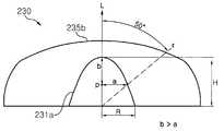
바람직하게, 상기 광학 부재는 광축(L), 입광부 및 상기 출광면을 가지며, 상기 입광부와 경계를 이루는 물질 및 상기 출광면과 경계를 이루는 물질보다 굴절율이 큰 재질로 이루어지도록 구성될 수 있다.Preferably, the optical member has an optical axis L, a light-incident portion, and the light-emitting surface, and may be made of a material having a higher refractive index than a material forming a boundary with the light-entering portion and a material having a boundary with the light- .
바람직하게, 상기 입광부는, 광축(L)으로부터 50도 내의 범위에서, 상기 광축(L) 상의 한 점(p)로부터 상기 입광부의 정점에 이르는 최단 거리가 상기 한점(p)으로부터 상기 입광부의 측면에 이르는 최단 거리(a)보다 큰 구조가 되도록 구성될 수 있다.Preferably, the light-incident portion has a shortest distance from a point p on the optical axis L to a vertex of the light-incident portion within a range of 50 degrees from the optical axis L, (A) leading to the side surface of the substrate.
바람직하게, 상기 출광면의 상부 중앙은 평탄면 또는 볼록한 곡면으로 형성되도록 구성될 수 있다.Preferably, the upper center of the light emitting surface is formed as a flat surface or a convex curved surface.
바람직하게, 상기 입광부는, 상기 발광 다이오드와 인접해 있는 하단 입구가 원형이며, 상기 정점을 향해 원형을 유지한 채 점진적으로 수렴되는 형상을 갖도록 구성될 수 있다.Preferably, the light-incident portion has a circular bottom shape adjacent to the light-emitting diode, and may have a shape gradually converging while maintaining a circular shape toward the vertex.
바람직하게, 상기 입광부의 높이는 상기 하단 입구 반경의 1.5배보다 크게 구성될 수 있다.Preferably, the height of the light-incident portion is greater than 1.5 times the radius of the lower end entrance.
바람직하게, 상기 입광부와 경계를 이루는 물질이 공기일 수 있다.Preferably, the material forming the boundary with the light-incident portion is air.
바람직하게, 상기 출광면과 경계를 이루는 물질이 공기일 수 있다.Preferably, the material forming the boundary with the light exiting surface is air.
바람직하게, 상기 광학 부재는 수지 또는 글래스 재질일 수 있다.Preferably, the optical member may be made of resin or glass.
본 발명의 다른 일 측면에 따르면, 전술한 바와 같은 백라이트 모듈; 및 직류 구동 전압을 상기 백라이트 모듈 내의 상기 복수의 MJT LED들에 제공하며, 상기 복수의 MJT LED들 각각의 구동을 독립적으로 제어하는 백라이트 제어모듈을 포함하는 것을 특징으로 하는 백라이트 유닛이 제안된다.According to another aspect of the present invention, there is provided a backlight module as described above; And a backlight control module for providing a DC driving voltage to the plurality of MJT LEDs in the backlight module and independently controlling driving of each of the plurality of MJT LEDs.
바람직하게, 상기 백라이트 제어모듈은 상기 직류 구동 전압을 상기 백라이트 모듈 내의 상기 복수의 MJT LED들 각각에 독립적으로 제공하며, 상기 백라이트 제어모듈은 디밍 신호에 따라 상기 복수의 MJT LED들 중 적어도 하나의 MJT LED에 제공되는 상기 직류 구동 전압을 PWM 제어함으로써 상기 적어도 하나의 MJT LED의 디밍 제어를 수행하도록 구성될 수 있다.Preferably, the backlight control module independently provides the DC driving voltage to each of the plurality of MJT LEDs in the backlight module, and the backlight control module controls at least one of the MJTs of the plurality of MJT LEDs And to perform dimming control of the at least one MJT LED by PWM control of the DC driving voltage provided to the LED.
바람직하게, 상기 백라이트 제어모듈은 상기 백라이트 모듈 내의 상기 복수의 MJT LED들 각각의 구동 전류를 독립적으로 검출 및 제어하도록 구성되며, 상기 백라이트 제어모듈은 디밍 신호에 따라 상기 복수의 MJT LED들 중 적어도 하나의 MJT LED의 구동 전류를 제어함으로써 상기 적어도 하나의 MJT LED의 디밍 제어를 수행하도록 구성될 수 있다.
Preferably, the backlight control module is configured to independently detect and control a driving current of each of the plurality of MJT LEDs in the backlight module, wherein the backlight control module is operable to control at least one of the plurality of MJT LEDs To control the dimming control of the at least one MJT LED by controlling the driving current of the MJT LED of the at least one MJT LED.
본 발명의 실시예들에 따르면, 소전류 구동 특성을 갖는 MJT LED를 이용하여 백라이트 모듈을 구성함으로써, 백라이트 모듈 및 이를 포함하는 백라이트 유닛의 소전류 구동이 가능하게 된다는 효과를 기대할 수 있다.According to the exemplary embodiments of the present invention, the backlight module can be constructed using the MJT LED having the small current driving characteristic, and the backlight module and the backlight unit including the backlight module can be driven with a small current.
또한, 본 발명의 실시예들에 따르면, 배선의 접속부들 중 하나를 발광셀의 경사진 측면에 전기적으로 접촉시킴으로써 MJT LED 칩의 각 발광셀의 유효 발광 면적을 증가시킬 수 있다는 효과를 기대할 수 있다.Further, according to the embodiments of the present invention, it is possible to increase the effective light emitting area of each light emitting cell of the MJT LED chip by electrically contacting one of the connection portions of the wiring with the inclined side face of the light emitting cell .
또한, 본 발명의 실시예들에 따르면, 백라이트 모듈의 구동을 제어하기 위한 구동회로의 안정성과 신뢰성을 개선하고, 제조 비용을 절감할 수 있는 효과를 기대할 수 있다.In addition, according to the embodiments of the present invention, it is possible to improve the stability and reliability of the driving circuit for controlling the driving of the backlight module and to reduce the manufacturing cost.
또한, 본 발명의 실시예들에 따르면, 백 라이트 유닛의 전력 효율 및 광 효율이 개선되고, 대전류 구동에 따른 드룹 현상을 방지할 수 있는 효과를 기대할 수 있다.According to the embodiments of the present invention, the power efficiency and the light efficiency of the backlight unit are improved, and the droop phenomenon caused by the driving of the large current can be prevented.
또한, 본 발명의 실시예들에 따르면, 백라이트 모듈을 구성하는 데 요구되는 LED의 수를 최소화하며, 백라이트 모듈을 구성하는 각각의 MJT LED별로 구동 제어가 가능하다는 효과를 기대할 수 있다.
In addition, according to embodiments of the present invention, it is possible to minimize the number of LEDs required to constitute the backlight module, and to control the driving of each MJT LED constituting the backlight module.
도 1은 종래기술에 따른 LED를 이용한 백라이트 유닛의 구성 블록도이다.
도 2는 본 발명의 일 실시예에 따른 MJT LED를 이용한 백라이트 유닛의 개략적인 구성 블록도이다.
도 3은 본 발명의 일 실시예에 따른 MJT LED 모듈을 설명하기 위한 개략적인 단면도이다.
도 4는 본 발명의 일 실시예에 따른 MJT LED를 설명하기 위한 개략적인 사시도이다.
도 5는 본 발명의 일 실시예에 따른 MJT LED 칩을 설명하기 위한 개략적인 평면도이다.
도 6은 본 발명의 일 실시예에 따른 MJT LED 칩을 설명하기 위해 도 5의 절취선 B-B를 따라 취해진 개략적인 단면도이다.
도 7 내지 도 13은 본 발명의 일 실시예에 따른 MJT LED 칩 제조방법을 설명하기 위한 개략적인 단면도들이다.
도 14은 본 발명의 또 다른 실시예에 따른 MJT LED 칩을 설명하기 위한 개략적인 단면도이다.
도 15 내지 도 18은 본 발명의 또 다른 실시예들에 따른 MJT LED 칩 제조방법을 설명하기 위한 개략적인 단면도들이다.
도 19는 광학 부재의 다양한 변형예를 설명하기 위한 단면도들이다.
도 20은 본 발명의 또 다른 실시예에 따른 MJT LED 모듈을 설명하기 위한 광학 부재의 단면도들이다.
도 21은 시뮬레이션에 사용된 MJT LED 모듈의 치수를 설명하기 위한 단면도이다.
도 22는 도 21의 광학 부재의 형상을 설명하기 위한 그래프들이다.
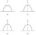
도 23은 도 21의 광학 부재의 광선 진행 방향을 나타낸다.
도 24는 조도 분포를 나타내는 그래프들로서, (a)는 MJT LED의 조도 분포를 나타내고, (b)는 광학 부재 사용에 따른 MJT LED 모듈의 조도 분포를 나타낸다.
도 25는 광 지향 분포를 나타내는 그래프들로서, (a)는 MJT LED의 광 지향 분포를 나타내고, (b)는 광학 부재 사용에 따른 MJT LED 모듈의 광 지향 분포를 나타낸다.
도 26은 본 발명의 일 실시예에 따른 MJT LED 모듈을 도시한 단면도이다.
도 27의 (a), (b) 및 (c)는 도 26의 a-a 선, b-b 선, c-c 선을 따라 취한 도면들이다.
도 28은 도 26에 도시된 MJT LED 모듈의 광학 부재를 보다 구체적으로 설명하기 위한 도면이다.
도 29는 도 28에 도시된 광학 부재 이용시의 광 지향각 분포를 보여주는 도면이다.
도 30은 본 발명의 다른 실시예에 따른 광학 부재를 설명하기 위한 도면이다.
도 31은 도 30의 광학 부재를 이용하여 얻을 수 있는 광 지향각 분포를 보여주는 도면이다.
도 32a 및 도 32b는 각각 비교예 1에 따른 광학 부재 및 지향각 분포 곡선을 보여주는 도면이다.
도 33a 및 도 33b는 각각 비교예 2에 따른 광학 부재 및 지향각 분포 곡선을 보여주는 도면이다.1 is a block diagram of a backlight unit using a conventional LED.
2 is a schematic block diagram of a backlight unit using an MJT LED according to an embodiment of the present invention.
3 is a schematic cross-sectional view illustrating an MJT LED module according to an exemplary embodiment of the present invention.
4 is a schematic perspective view illustrating an MJT LED according to an exemplary embodiment of the present invention.
5 is a schematic plan view illustrating an MJT LED chip according to an embodiment of the present invention.
FIG. 6 is a schematic cross-sectional view taken along the cutting line BB of FIG. 5 to illustrate an MJT LED chip according to an embodiment of the present invention.
FIGS. 7 to 13 are schematic cross-sectional views illustrating a method of manufacturing an MJT LED chip according to an embodiment of the present invention.
14 is a schematic cross-sectional view illustrating an MJT LED chip according to another embodiment of the present invention.
15 to 18 are schematic cross-sectional views for explaining a method of manufacturing an MJT LED chip according to still another embodiment of the present invention.
19 is a sectional view for explaining various modifications of the optical member.
20 is a sectional view of an optical member for explaining an MJT LED module according to another embodiment of the present invention.
21 is a sectional view for explaining the dimensions of the MJT LED module used in the simulation.
22 is a graph for explaining the shape of the optical member of Fig.
Fig. 23 shows the light traveling direction of the optical member in Fig.
24 is a graph showing the illuminance distribution, in which (a) shows the illuminance distribution of the MJT LED, and (b) shows the illuminance distribution of the MJT LED module according to the use of the optical member.
FIG. 25 is a graph showing the light-directed distribution, in which (a) shows the light-oriented distribution of the MJT LED, and (b) shows the light-oriented distribution of the MJT LED module according to the use of the optical member.
26 is a cross-sectional view illustrating an MJT LED module according to an embodiment of the present invention.
Figures 27 (a), (b) and (c) are views taken along lines aa, bb, and cc in Figure 26.
28 is a view for more specifically explaining the optical member of the MJT LED module shown in Fig.
29 is a view showing the light-directed angular distribution when the optical member shown in Fig. 28 is used.
30 is a view for explaining an optical member according to another embodiment of the present invention.
31 is a view showing a light directing angle distribution obtained by using the optical member of Fig.
32A and 32B are views showing the optical member and the directivity distribution curve according to Comparative Example 1, respectively.
33A and 33B are views showing the optical member and the directivity distribution curve according to Comparative Example 2, respectively.
후술하는 본 발명에 대한 상세한 설명은, 본 발명이 실시될 수 있는 특정 실시예를 예시로서 도시하는 첨부 도면을 참조한다. 이들 실시예는 당업자가 본 발명을 실시할 수 있기에 충분하도록 상세히 설명된다. 본 발명의 다양한 실시예는 서로 다르지만 상호 배타적일 필요는 없음이 이해되어야 한다. 예를 들어, 여기에 기재되어 있는 특정 형상, 구조 및 특성은 일 실시예에 관련하여 본 발명의 정신 및 범위를 벗어나지 않으면서 다른 실시예로 구현될 수 있다. 또한, 각각의 개시된 실시예 내의 개별 구성요소의 위치 또는 배치는 본 발명의 정신 및 범위를 벗어나지 않으면서 변경될 수 있음이 이해되어야 한다. 따라서, 후술하는 상세한 설명은 한정적인 의미로서 취하려는 것이 아니며, 본 발명의 범위는 적절하게 설명된다면 그 청구항들이 주장하는 것과 균등한 모든 범위와 더불어 첨부된 청구항에 의해서만 한정된다. 도면에서 유사한 참조부호는 여러 측면에 걸쳐서 동일하거나 유사한 기능을 지칭한다.The following detailed description of the invention refers to the accompanying drawings, which illustrate, by way of illustration, specific embodiments in which the invention may be practiced. These embodiments are described in sufficient detail to enable those skilled in the art to practice the invention. It should be understood that the various embodiments of the present invention are different, but need not be mutually exclusive. For example, certain features, structures, and characteristics described herein may be implemented in other embodiments without departing from the spirit and scope of the invention in connection with an embodiment. It is also to be understood that the position or arrangement of the individual components within each disclosed embodiment may be varied without departing from the spirit and scope of the invention. The following detailed description is, therefore, not to be taken in a limiting sense, and the scope of the present invention is to be limited only by the appended claims, along with the full scope of equivalents to which the claims are entitled, if properly explained. In the drawings, like reference numerals refer to the same or similar functions throughout the several views.
이하, 본 발명이 속하는 기술분야에서 통상의 지식을 가진 자가 본 발명을 용이하게 실시할 수 있도록 하기 위하여, 본 발명의 바람직한 실시예들에 관하여 첨부된 도면을 참조하여 상세히 설명하기로 한다.
Hereinafter, preferred embodiments of the present invention will be described in detail with reference to the accompanying drawings, so that those skilled in the art can easily carry out the present invention.
[본 발명의 바람직한 실시예][Preferred Embodiment of the Present Invention]
본 발명의 실시예에서, 용어 "MJT LED 칩"이란 하나의 LED 칩 내에 복수의 발광셀들이 배선들에 의해 서로 연결되어 있는 멀티-셀 LED 칩을 의미한다. 또한 MJT LED 칩은 N개의 발광셀들을 포함하여 구성될 수 있으며(N은 2 이상의 양의 정수), N은 필요에 따라 다양하게 설정될 수 있다. 또한, 각 발광셀의 순방향 전압은, 바람직하게, 3V ~ 3.6V 사이일 수 있으나 이에 한정되는 것은 아니다. 따라서, MJT LED 칩(또는 MJT LED)의 순방향 전압은 해당 MJT LED 칩 내에 포함된 발광셀들의 수에 비례한다. MJT LED 칩 내에 포함되는 발광셀들 수가 필요에 따라 다양하게 구성될 수 있기 때문에, 본 발명에 따른 MJT LED 칩은 백라이트 유닛에 사용되는 구동 전원 생성부(예를 들어, DC 컨버터)의 사양에 따라 6~36V의 구동전압을 갖도록 구성될 수 있으나, 이에 한정되는 것은 아니다. 또한, MJT LED 칩의 구동 전류는 종래의 단일-셀 LED에 비하여 매우 작으며, 예를 들어, 바람직하게 20mA ~ 40mA 사이일 수 있으나, 이에 한정되는 것은 아니다.In the embodiment of the present invention, the term "MJT LED chip" means a multi-cell LED chip in which a plurality of light emitting cells are connected to each other by wiring lines in one LED chip. Also, the MJT LED chip may be configured to include N light emitting cells (N is a positive integer of 2 or more), and N may be variously set as needed. In addition, the forward voltage of each light emitting cell may preferably be between 3V and 3.6V, but is not limited thereto. Thus, the forward voltage of the MJT LED chip (or MJT LED) is proportional to the number of light emitting cells contained in the MJT LED chip. Since the number of light emitting cells included in the MJT LED chip can be variously configured as needed, the MJT LED chip according to the present invention can be manufactured in accordance with the specification of the driving power generating unit (for example, a DC converter) used in the backlight unit May be configured to have a driving voltage of 6 to 36 V, but the present invention is not limited thereto. In addition, the driving current of the MJT LED chip is very small compared to conventional single-cell LEDs, for example, but is not limited to, 20mA to 40mA.
또한, 용어 "MJT LED"란 본 발명에 따른 MJT LED 칩을 실장하고 있는 발광 소자 또는 LED 패키지를 지칭한다.Further, the term "MJT LED" refers to a light emitting device or an LED package mounting the MJT LED chip according to the present invention.
또한, 용어 "MJT LED 모듈"이란 하나의 MJT LED와 대응하는 하나의 광학 부재를 결합한 구성요소를 지칭한다. 대응하는 광학 부재는 MJT LED에 직접 배치될 수도 있으며, 또는 MJT LED가 실장된 인쇄회로기판에 배치될 수도 있다. 광학 부재의 배치방식과 무관하게, 하나의 MJT LED와 대응하는 하나의 광학 부재가 결합되어 지칭되는 경우 MJT LED 모듈이라 한다.Further, the term "MJT LED module" refers to a component that combines one MJT LED and a corresponding one optical member. The corresponding optical element may be placed directly on the MJT LED, or on a printed circuit board on which the MJT LED is mounted. Irrespective of the arrangement of the optical members, when one MJT LED and one corresponding optical member are referred to as being combined, it is referred to as an MJT LED module.
또한, 용어 "백라이트 모듈"이란 인쇄회로기판 상에 복수의 MJT LED들이 배치되고, 복수의 MJT LED들 각각에 대응하는 복수의 광학 부재들이 배치된 조명 모듈을 의미한다. 따라서, 용어 "백라이트 모듈"은 인쇄회로기판 상에 복수의 MJT LED 모듈들이 소정의 규칙에 따라 실장된 조명 모듈을 의미할 수 있다. 한편, 일 실시예에 있어 본 발명에 따른 백라이트 모듈은 직하형 백라이트 모듈일 수 있으나 본 발명이 이에 한정되는 것은 아니며, 본 발명에 따른 백라이트 모듈이 다른 실시예에 있어 면 조명용 광원으로 사용될 수도 있다. 따라서, 그 명칭에 불구하고 본 발명에 따른 백라이트 모듈의 기술적 요지를 포함하고 있는 한, 본 발명의 권리범위에 속함은 당업자에게 자명할 것이다.
Further, the term "backlight module" means a lighting module in which a plurality of MJT LEDs are disposed on a printed circuit board and a plurality of optical members corresponding to each of the plurality of MJT LEDs are disposed. Thus, the term "backlight module" may refer to a lighting module in which a plurality of MJT LED modules are mounted on a printed circuit board according to a predetermined rule. Meanwhile, in one embodiment, the backlight module according to the present invention may be a direct-type backlight module, but the present invention is not limited thereto, and the backlight module according to the present invention may be used as a light source for area illumination in another embodiment. Accordingly, it will be apparent to those skilled in the art, to the extent that they fall within the scope of the present invention, as long as they include the technical gist of the backlight module according to the present invention in spite of its name.
MJTMJT LED를 이용한 백라이트 유닛의 개괄 An overview of backlight units using LEDs
본 발명에 따른 백라이트 유닛의 구성을 구체적으로 설명하기에 앞서, 본 발명의 중요한 기술적 특징에 대하여 살펴보도록 한다. 본 발명은 전술한 바와 같은 종래기술의 문제점을 해결하기 위하여 MJT LED가 갖는 소자적 특성에 착안하여 안출된 발명이다. 즉, 본 발명은 종래기술에 따른 단일-셀 LED가 갖는 소전압 대전류 구동 특성에 따른 문제점을 해결하기 위하여, MJT LED가 갖는 대전압 소전류 구동 특성(예를 들어, 6~36V의 구동 전압 및 20~40mA의 구동 전류)에 착안하였으며, 이러한 MJT LED를 이용하여 백라이트 모듈을 구성함으로써 전술한 바와 같은 종래기술에 따른 문제점들을 해결하고자 하였다. 전술한 바와 같이, MJT LED의 경우 종래의 단일-셀 LED와 달리 임의의 수의 발광셀을 포함할 수 있으며, 포함되는 발광셀의 수에 따라 순방향 전압이 달라지는 특성을 가지고 있다. 또한, MJT LED의 경우 복수의 발광셀을 포함하고 있으므로 종래의 단일-셀 LED에 비하여 넓은 범위를 조사할 수 있고, 또한 하나의 MJT LED 칩으로 구성되므로 이에 대한 광학 부재를 설계하고 적용하기에 용이하다. 따라서, 이러한 MJT LED를 이용하는 경우, 액정패널의 복수의 분할 영역 중 하나의 분할 영역을 MJT LED 모듈(MJT LED+광학 부재) 하나로 커버할 수 있게 된다. 따라서, 백라이트 모듈을 구성하는데 요구되는 LED들의 수가 종래의 단일-셀 LED에 비하여 줄어들게 된다. 결론적으로, 본 발명은 복수의 MJT LED 모듈을 이용하여 백라이트 모듈을 구성하고, 백라이트 모듈을 구성하는 각각의 MJT LED들을 각기 독립적으로 제어하도록 백라이트 유닛을 구성함으로써 본 발명의 목적을 달성할 수 있도록 구성된다.Before describing the configuration of the backlight unit according to the present invention, important technical features of the present invention will be described. SUMMARY OF THE INVENTION The present invention has been made in view of the elemental characteristics of the MJT LED in order to solve the problems of the conventional art as described above. That is, in order to solve the problem caused by the small-voltage high current driving characteristic of the single-cell LED according to the related art, the present invention provides a large-voltage small current driving characteristic (for example, 20 to 40 mA of driving current), and the backlight module is constructed using the MJT LED to solve the above-described problems in the related art. As described above, the MJT LED may include any number of light emitting cells unlike the conventional single-cell LED, and has a characteristic that the forward voltage varies depending on the number of the light emitting cells included therein. In addition, since the MJT LED includes a plurality of light emitting cells, it can be irradiated over a wide range compared with the conventional single-cell LED, and is composed of one MJT LED chip, so that the optical member can be easily designed and applied Do. Therefore, when such an MJT LED is used, one of the plurality of divided regions of the liquid crystal panel can be covered with one MJT LED module (MJT LED + optical member). Thus, the number of LEDs required to construct the backlight module is reduced compared to conventional single-cell LEDs. In conclusion, the present invention provides a backlight module using a plurality of MJT LED modules and a backlight unit for independently controlling each of the MJT LEDs constituting the backlight module, thereby achieving the object of the present invention do.
이하에서, 도 2 내지 도 4를 참조하여, 본 발명의 바람직한 일 실시예에 따른 백라이트 유닛(1000)에 대하여 보다 구체적으로 살펴보도록 한다.Hereinafter, a
먼저, 도 2는 본 발명의 바람직한 일 실시예에 따른 MJT LED를 이용한 백라이트 유닛의 개략적인 구성 블록도이다. 도 2에 도시된 바와 같이, 본 발명에 따른 백라이트 유닛(1000)은 백라이트 제어모듈(400) 및 백라이트 모듈(300)을 포함할 수 있다.2 is a schematic block diagram of a backlight unit using an MJT LED according to a preferred embodiment of the present invention. 2, the
보다 구체적으로, 본 발명에 따른 백라이트 제어모듈(400)은 외부로부터 입력되는 입력 전원(Vin)을 이용하여 DC 구동 전원을 생성/출력하는 구동 전원 생성부(410) 및 백라이트 모듈(300)을 구성하는 복수의 MJT LED들(100) 각각의 동작을 제어(온/오프 제어 및 디밍 제어)하는 구동 제어부(420)를 포함하여 구성된다. 구동 전원 생성부(410)는 일반적으로 12V, 24V, 48V 등의 안정적인 DC 전압을 구동 전원으로 생성하여 백라이트 모듈(300)을 구성하는 복수의 MJT LED들(100)에 제공하도록 구성된다. 이때, 구동 전원 생성부(410)에 공급되는 입력 전원(Vin)은 220V 또는 110V의 상용 교류전원일 수 있다. 이러한 구동 전원 생성부(410)는 도 1에 도시된 종래기술에 따른 구동 전원 생성부(410)와 실질적으로 동일하게 구성될 수 있다.More specifically, the
본 발명에 따른 백라이트 모듈(300)은 인쇄회로기판(도 2에는 미도시됨) 상에 복수의 MJT LED들(100) 및 각각의 MJT LED(100)에 대응하는 광학 부재(도 2에는 미도시됨)를 규칙적으로(예를 들어, 매트릭스 형태로) 배치함으로써 구성될 수 있다. 도 2에 도시된 실시예에 있어, 백라이트 모듈(300) 내에서 가로 방향으로 M개의 MJT LED들(100)이 배치되고, 세로 방향으로 N개의 MJT LED들(100)이 배치되어 MxN 매트릭스 배열을 구성하는 것으로 가정한다. 또한, 좌측 최상단에 배치되는 MJT LED를 제 1-1 MJT LED(100_11)로 지칭하며 우측 최하단에 배치되는 MJT LED를 제 M-N MJT LED(100_MN)로 지칭한다.The
한편, 여기서 가장 주목해야 할 점은, 도 1에 도시된 종래기술과 달린 도 2에 도시된 실시예의 백라이트 모듈(300) 내의 MJT LED들(100)은 서로 직렬 또는 병렬 또는 직/병렬로 연결되지 않고 각기 독립적으로 구동 전원 생성부(410) 및 구동 제어부(420)에 연결되도록 구성된다는 점이다. 즉, 도 2에 도시된 실시예에 있어, 각 MJT LED(100)의 애노드단이 독립적으로 구동 전원 생성부(410)에 연결되며, 각 MJT LED(100)의 캐소드단이 독립적으로 구동 제어부(420)에 연결된다.It should be noted that the
이러한 구성으로 인하여, 본 발명에 따른 구동 제어부(420)는 백라이트 모듈(300)을 구성하는 복수의 MJT LED들(100) 각각의 동작을 독립적으로 제어할 수 있게 된다. 보다 구체적으로, 본 발명에 따른 구동 제어부(420)는 디밍 신호(Dim)에 따라 복수의 MJT LED들(100) 중 특정 MJT LED의 디밍 레벨을 제어하도록 구성된다.With this configuration, the driving
일 실시예에 있어, 본 발명에 따른 구동 제어부(420)는 PWM 제어 수단(미도시)을 포함하며, MJT LED들(100) 중 디밍 제어 대상이 되는 특정 MJT LED에 공급되는 구동 전원을 PWM(Pulse Width Modulation) 제어함으로써 디밍 제어를 수행하도록 구성될 수 있다. 특히, 도 1에 도시되어 있는 종래기술과 달리, 도 2에 도시되어 있는 본 발명에 따른 백라이트 유닛(1000)은 복수의 MJT LED들(100) 각각이 서로 독립적으로 구동 전원 생성부(410)에 연결되어 독립적으로 구동 전원을 공급받도록 구성되어 있기 때문에, 이러한 PWM 제어 방식의 디밍 제어가 가능해 진다. 예를 들어, 제 1-1 MJT LED(100_11)에 대한 디밍 제어가 필요한 경우, 구동 제어부(420)는 생성된 구동 전원을 디밍 신호(Dim)에 따라 소정의 듀티비(예를 들어, 60%)로 펄스 폭 변조하고, 펄스 폭 변조된 구동 전원을 제 1-1 MJT LED(100_11)에 제공함으로써 제 1-1 MJT LED(100_11)에 대한 디밍 제어를 수행할 수 있다. 이때, 제 1-1 MJT LED(100_11) 외의 다른 MJT LED들에는 펄스 폭 변조되지 않은 듀티비가 100%인 구동 전원이 공급될 것이다. 또는, 이때, 제 1-1 MJT LED(100_11) 외의 다른 MJT LED들에는 정상 듀티비(별도의 디밍 제어가 없을 때 기본적으로 갖는 듀티비, 예를 들어, 80%)로 펄스 폭 변조된 구동 전원이 공급될 것이다. 따라서, 제 1-1 MJT LED(100_11)만에 대한 로컬 디밍이 가능하게 된다. 물론, 복수의 MJT LED들에 대하여 동시에 PWM 제어를 이용하여 동일한 디밍 레벨로 및/또는 각각의 MJT LED별로 상이한 디밍 레벨들로 디밍 제어가 가능하다는 것이 당업자에게 자명할 것이다. 구동 전원을 PWM 제어하기 위한 PWM 제어 수단 자체는 이미 공지된 기술을 채택하고 있는바, 더 이상의 상세한 설명은 생략하기로 한다.In one embodiment, the driving
한편, 다른 실시예에 있어, 본 발명에 따른 구동 제어부(420)는 구동 전류 검출 수단(미도시) 및 구동 전류 제어 수단(미도시)을 포함하며, MJT LED들(100) 중 디밍 제어 대상이 되는 특정 MJT LED에 공급되는 구동 전류를 제어함으로써 디밍 제어를 수행하도록 구성될 수 있다. 특히, 도 1에 도시되어 있는 종래기술과 달리, 도 2에 도시되어 있는 본 발명에 따른 백라이트 유닛(1000)은 복수의 MJT LED들(100) 각각이 서로 독립적으로 구동 제어부(420)에 연결되어 있으므로, 이러한 방식의 MJT LED별 구동 전류 제어 방식의 디밍 제어가 가능해 진다. 이때, 구동 제어부(420)에 포함되는 구동 전류 검출 수단 및 구동 전류 제어 수단은 MJT LED들(100) 각각에 1 대 1로 대응하게 된다. 따라서, 전술한 바와 같이 MxN개의 MJT LED들(100)로 백라이트 모듈(300)이 구성되는 경우, MxN개의 구동 전류 검출 수단 및 구동 전류 제어 수단이 구동 제어부(420)에 포함된다. 예를 들어, 제 M-N MJT LED(100_MN)에 대한 디밍 제어가 필요한 경우, 구동 제어부(420)는 구동 전류 검출 수단을 이용하여 현재 제 M-N MJT LED(100_MN)에 흐르는 구동 전류를 검출하고, 디밍 신호(Dim)에 따라 제 M-N MJT LED(100_MN)에 흐르는 구동 전류의 값을 변경함으로써(예를 들어, 최대 구동 전류의 100%로) 제 M-N MJT LED(100_MN)에 대한 디밍 제어를 수행하게 된다. 이때, 제 M-N MJT LED(100_MN) 외의 다른 MJT LED들에는 정상 구동 전류(별도의 디밍 제어가 없을 때 기본적으로 설정된 구동 전류, 예를 들어, 최대 구동 전류의 80%)가 흐르게 되므로, 제 M-N MJT LED(100_MN)만에 대한 로컬 디밍이 가능하게 된다. 물론, 복수의 MJT LED들에 대하여 동시에 구동 전류 제어를 통해 동일한 디밍 레벨로 및/또는 각각의 MJT LED별로 상이한 디밍 레벨들로 디밍 제어가 가능하다는 것이 당업자에게 자명할 것이다. 한편, 이러한 실시예에 있어 MJT LED들(100)이 각기 독립적으로 구동 전원을 공급받아야할 필요성이 없기 때문에, 도 2에 도시된 실시예와 달리, 각 MJT LED(100)의 애노드단이 구동 전원 생성부(410)에 연결된 하나의 구동 전원 라인에 각기 병렬로 연결되도록 구성될 수도 있다. 구동 전류 검출 수단 및 구동 전류 제어 수단 자체는 이미 공지된 기술을 채택하고 있는바, 더 이상의 상세한 설명은 생략하기로 한다.
In another embodiment, the driving
MJTMJTLEDLED 및 AndMJTMJTLEDLED 모듈의 개괄 Overview of modules
도 3은 본 발명의 일 실시예에 따른 MJT LED 모듈을 설명하기 위한 개략적인 단면도이고, 도 4는 MJT LED 모듈에 사용되는 MJT LED를 설명하기 위한 사시도이다. 이하에서, 도 3 및 도 4를 참조하여 본 발명에 따른 MJT LED(100) 및 MJT LED 모듈의 구체적인 구성을 살펴보도록 한다.FIG. 3 is a schematic cross-sectional view illustrating an MJT LED module according to an exemplary embodiment of the present invention, and FIG. 4 is a perspective view illustrating an MJT LED used in an MJT LED module. Hereinafter, a specific configuration of the
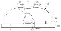
도 3을 참조하면, MJT LED 모듈은 MJT LED(100) 및 광학 부재(130)를 포함한다. MJT LED(100)가 인쇄회로기판(110) 상에 실장되며, 대응하는 광학 부재(130)가 MJT LED(100)와 정합되는 위치에서 인쇄회로기판(110) 상에 실장된다. 전술한 바와 같이 다른 실시예에 있어 광학 부재(130)가 MJT LED(100)에 직접적으로 연결될 수도 있다. 인쇄회로기판(110)은 일부가 도시되어 있지만, 하나의 인쇄회로기판(110) 상에 복수의 MJT LED들(100) 및 그에 대응하는 광학 부재들(130)이 매트릭스 또는 벌집 모양 등 다양하게 배열되어 전술한 바와 같은 백라이트 모듈(300)을 구성하게 된다.Referring to FIG. 3, the MJT LED module includes an
인쇄회로기판(110)은 MJT LED(100)의 단자들이 본딩되는 도전성의 랜드 패턴들을 상면에 포함한다. 또한, 인쇄회로기판(110)은 상면에 반사막을 포함할 수 있다. 인쇄회로기판(110)은 열전도성이 좋은 금속을 기반으로 하는 MCPCB(Metal-Core PCB)일 수 있다. 또한, 인쇄회로기판(110)은 FR4와 같은 절연성 기판 재료를 기반으로 할 수 있다. 도시하지는 않았지만, 인쇄회로기판(110)의 하부에는 MJT LED(100)에서 발생된 열을 방출하기 위해 히트싱크가 배치될 수 있다.The printed
MJT LED(100)는, 도 4에 잘 도시된 바와 같이, 하우징(121)과, 하우징(121) 상에 실장된 MJT LED 칩(123) 및 MJT LED 칩(123)을 덮는 파장 변환층(125)을 포함할 수 있다. MJT LED(100)는 또한 하우징(121)에 지지된 리드 단자들(도시하지 않음)을 포함한다.4, the
패키지 몸체를 구성하는 하우징(121)은 PA 또는 PPA 등과 같은 플라스틱 수지를 사출 성형하여 만들어질 수 있다. 이 경우, 하우징(121)은 사출 성형 공정에 의해 리드 단자들을 지지하는 상태로 성형될 수 있으며, 또한 MJT LED 칩(123)을 실장하기 위한 캐비티(121a)를 가질 수 있다. 캐비티(121a)는 MJT LED(100)의 광 출사 영역을 정의한다.The
리드 단자들은 하우징(121) 내에서 서로 이격되게 배치되며, 하우징(121) 외부로 연장되어 인쇄회로기판(110) 상의 랜드 패턴에 본딩된다.The lead terminals are spaced apart from each other in the
MJT LED 칩(123)은 캐비티(121a) 바닥에 실장되어 리드 단자들에 전기적으로 연결된다. MJT LED 칩(123)은 자외선 또는 청색광을 방출하는 질화갈륨 계열의 MJT LED일 수 있다. 본 발명에 따른 MJT LED 칩(123)의 상세 구성과 그 제조 방법에 대해서는 도 5 내지 도 18을 참조하여 후술하도록 한다.The
한편, 파장 변환층(125)이 MJT LED 칩(123)을 덮는다. 일 실시예에서, 파장 변환층(125)은 MJT LED 칩(123)을 실장한 후, 형광체를 함유하는 몰딩수지로 캐비티(121a)를 채워 형성될 수 있다. 이때, 파장 변환층(125)은 하우징(121)의 캐비티(121a)를 채우고 상면이 실질적으로 평평하거나 또는 볼록할 수 있다. 또한, 파장 변환층(125) 상에 광학 부재 형상을 갖는 몰딩 수지가 더 형성될 수도 있다.On the other hand, the
다른 실시예에서, 컨포멀한 형광체 코팅층이 형성된 MJT LED 칩(123)이 하우징(121) 상에 실장될 수 있다. 즉, MJT LED 칩(123) 상에 형광체의 컨포멀 코팅층을 적용하고, 이 형광체 코팅층을 갖는 MJT LED 칩(123)을 하우징(121) 상에 실장할 수 있다. 컨포멀 코팅층을 갖는 MJT LED 칩(123)은 투명 수지에 의해 몰딩될 수 있다. 나아가, 이 몰딩 수지는 광학 부재 형상을 가질 수 있으며, 따라서 1차 광학 부재로서 기능할 수 있다.In another embodiment, the
파장 변환층(125)은 MJT LED 칩(123)에서 방출된 광을 파장 변환하여 혼색광, 예컨대 백색광을 구현한다.The
MJT LED(100)는 거울면 대칭 구조의 광 지향 분포를 갖도록 설계되며, 특히 회전 대칭 구조의 광 지향 분포를 갖도록 설계될 수 있다. 이때, 광 지향 분포의 중심을 향하는 MJT LED의 축이 광축(L)으로 정의된다. 즉, MJT LED(100)는 광축(L)을 중심으로 좌우 대칭인 광 지향 분포를 갖도록 설계된다. 일반적으로, 하우징(121)의 캐비티(121a)가 거울면 대칭 구조를 갖도록 형성될 수 있으며, 광축(L)은 캐비티(121a)의 중심을 지나는 직선으로 정의될 수 있다.The
광학 부재(130)는 MJT LED(100)로부터 광을 입사받는 입광면 및 MJT LED(100)의 광 지향각 보다 넓은 광 지향각으로 광을 출사하는 출광면을 포함하여 구성되어, MJT LED(100)로부터 출사되는 광을 고르게 분산시키는 기능을 수행하게 된다. 이러한 본원발명에 따른 광학 부재(130)에 대해서는 도 19 내지 도 33을 참조하여 후술하도록 한다.
The
MJTMJTLEDLED 칩의 구성 및 그 제조 방법 Configuration of chip and method of manufacturing thereof
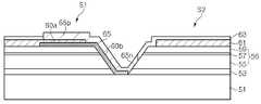
이하에서, 전술한 바와 같이 본 발명에 따른 MJT LED(100)에 실장되는 MJT LED 칩(123)의 구성과 그 제조 방법에 대하여 도 5 내지 도 18을 참조하여 상세하게 살펴보도록 한다.Hereinafter, the structure and manufacturing method of the
도 5는 본 발명의 일 실시예에 따른 MJT LED 칩을 설명하기 위한 개략적인 평면도이고, 도 6은 도 5의 절취선 B-B를 따라 취해진 단면도이다.FIG. 5 is a schematic plan view for explaining an MJT LED chip according to an embodiment of the present invention, and FIG. 6 is a sectional view taken along the cutting line B-B in FIG.
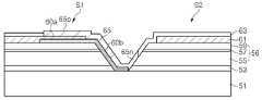
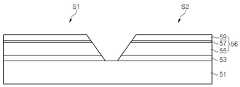
도 5 및 도 6을 참조하면, MJT LED 칩(123)은 성장 기판(51), 발광셀들(S1, S2), 투명전극층(61), 전류 차단층(60a), 절연층(60b), 절연 보호층(63) 및 배선(65)를 포함한다. 또한, MJT LED 칩(123)은 버퍼층(53)을 포함할 수 있다.5 and 6, the
성장 기판(51)은 절연 또는 도전성 기판일 수 있으며, 예컨대 사파이어 기판, 질화갈륨 기판, 탄화실리콘(SiC) 기판 또는 실리콘 기판일 수 있다. 나아가, 성장 기판(51)은 패터닝된 사파이어 기판과 같이 상면에 요철 패턴(도시하지 않음)을 갖는 성장 기판일 수 있다.The
단일 성장 기판(51) 상에 제1 발광셀(S1) 및 제2 발광셀(S2)이 이격되어 위치한다. 제1 및 제2 발광셀들(S1, S2) 각각은 하부 반도체층(55), 하부 반도체층의 일 영역 상에 위치하는 상부 반도체층(59) 및 하부 반도체층과 상부 반도체층 사이에 개재된 활성층(57)을 포함하는 적층 구조(56)를 갖는다. 여기서, 하부 및 상부 반도체층은 각각 n형 및 p형인 것으로 설명하지만, 그 반대일 수도 있다.The first light emitting cell S1 and the second light emitting cell S2 are spaced apart from each other on the
하부 반도체층(55), 활성층(57) 및 상부 반도체층(59)은 각각 질화갈륨 계열의 반도체 물질 즉, (Al, In, Ga)N으로 형성될 수 있다. 활성층(57)은 요구되는 파장의 광 예컨대 자외선 또는 청색광을 방출하도록 조성 원소 및 조성비가 결정되며, 하부 반도체층(55) 및 상부 반도체층(59)은 활성층(57)에 비해 밴드갭이 큰 물질로 형성된다.The
하부 반도체층(55) 및/또는 상부 반도체층(59)은, 도시한 바와 같이, 단일층으로 형성될 수 있으나, 다층 구조로 형성될 수도 있다. 또한, 활성층(57)은 단일 양자웰 또는 다중 양자웰 구조를 가질 수 있다. The
제1 및 제2 발광셀들(S1, S2)은 경사진 측면을 가질 수 있으며, 측면의 경사각은 성장 기판(51) 상부면에 대해 예컨대 15도 내지 80도 범위 내 일 수 있다. The first and second light emitting cells S1 and S2 may have inclined side surfaces and the inclination angle of the side surfaces may be in the range of 15 to 80 degrees with respect to the upper surface of the
활성층(57) 및 상부 반도체층(59)이 하부 반도체층(55)의 상에 위치한다. 하부 반도체층(55)의 상면은 활성층(57)에 의해 완전히 덮일 수 있으며, 그 측면만이 노출될 수 있다. The
도 6에서, 제1 발광셀(S1)과 제2 발광셀(S2)의 일부를 도시하고 있지만, 제1 발광셀(S1)과 제2 발광셀(S2)은 도 5에 도시한 바와 같이 유사하거나 동일한 구조를 가질 수 있다. 즉, 제1 발광셀(S1)과 제2 발광셀(S2)은 동일한 질화갈륨계 반도체 적층 구조를 가질 수 있으며, 또한 동일한 구조의 경사진 측면을 가질 수 있다.6, a part of the first light emitting cell S1 and the second light emitting cell S2 are shown, but the first light emitting cell S1 and the second light emitting cell S2 are similar to each other as shown in Fig. 5 Or may have the same structure. That is, the first light emitting cell S1 and the second light emitting cell S2 may have the same gallium nitride semiconductor laminated structure, and may have inclined side surfaces of the same structure.
한편, 발광셀들(S1, S2)과 성장 기판(51) 사이에 버퍼층(53)이 개재될 수 있다. 버퍼층(53)은, 성장 기판(51)과 그 위에 형성될 하부 반도체층(55)의 격자부정합을 완화시키기 위해 채택된다.On the other hand, a
투명 전극층(61)은 각 발광셀(S1, S2) 상에 위치한다. 즉, 제1 투명 전극층(61)이 제1 발광셀(S1) 상에 위치하며, 제2 투명 전극층(61)이 제2 발광셀(S2) 상에 위치한다. 투명 전극층(61)은 상부 반도체층(59) 상부면 상에 위치하여 상부 반도체층(59)에 접속할 수 있으며, 상부 반도체층(59)의 면적보다 좁은 면적을 가질 수 있다. 즉, 투명 전극층(61)은 상부 반도체층(59)의 가장자리로부터 리세스될 수 있다. 따라서, 투명 전극층(61)의 가장자리에서 발광셀(S1, S2)의 측벽을 통해 전류가 집중되는 것을 방지할 수 있다.The
한편, 전류 차단층(60a)은 각 발광셀(S1, S2) 상에 위치할 수 있으며, 투명 전극층(61)과 발광셀(S1, S2) 사이에 위치한다. 투명 전극층(61)의 일부는 전류 차단층(60a) 상에 위치한다. 전류 차단층(60a)은 각 발광셀(S1, S2)의 가장자리 근처에 위치할 수 있으나, 이에 한정되는 것은 아니며, 각 발광셀(S1, S2)의 중앙 영역에 위치할 수도 있다. 전류 차단층(60a)은 절연물질로 형성되며, 특히 굴절률이 서로 다른 층들을 교대로 적층한 분포 브래그 반사기를 포함할 수 있다.The
한편, 절연층(60b)이 제1 발광셀(S1)의 측면 일부를 덮는다. 도 5 및 도 6에 도시한 바와 같이, 절연층(60b)은 제1 발광셀(S1)과 제2 발광셀(S2) 사이의 영역으로 연장할 수 있으며, 나아가, 제2 발광셀(S2)의 하부 반도체층(55)의 측면 일부를 덮을 수도 있다. 절연층(60b)은 전류 차단층(60a)과 동일 구조 및 동일 재료로 형성될 수 있으며, 분포 브래그 반사기를 포함할 수 있으나, 이에 한정되는 것은 아니다. 절연층(60b)은 전류 차단층(60a)과 다른 공정에 의해 다른 재료로 형성될 수도 있다. 다만, 절연층(60b)이 다중층인 분포 브래그 반사기를 포함할 경우, 절연층(60b) 내에 핀홀과 같은 결함이 발생하는 것을 효율적으로 억제할 수 있다. 절연층(60b)은 전류 차단층(60a)에 연결되어 연속적으로 위치할 수 있으나, 본 발명이 반드시 이에 한정되는 것은 아니다. 절연층(60b)과 전류 차단층(60a)은 서로 이격되어 배치될 수도 있다.On the other hand, the insulating
배선(65)은 제1 발광셀(S1)과 제2 발광셀(S2)을 전기적으로 연결한다. 배선(65)은 제1 접속부(65p)와 제2 접속부(65n)를 포함한다. 제1 접속부(65p)는 제1 발광셀(S1) 상의 투명 전극층(61)에 전기적으로 접속되고, 제2 접속부(65n)는 제2 발광셀(S2)의 하부 반도체층(55)에 전기적으로 접속된다. 제1 접속부(65p)는 제1 발광셀(S1)의 일측 가장자리에 가깝게 배치될 수 있으나, 이에 한정되는 것은 아니며, 제1 발광셀(S1)의 중앙 영역에 배치될 수도 있다.The
제2 접속부(65n)는 제2 발광셀(S2)의 경사진 측면, 특히 제2 발광셀(S2)의 하부 반도체층(55)의 경사진 측면에 접촉할 수 있다. 또한, 제2 접속부(65n)는 도 5에 도시한 바와 같이, 제2 발광셀(S2)의 둘레를 따라 양측으로 연장하면서 하부 반도체층(55)의 경사진 측면에 전기적으로 접촉할 수 있다. 배선(65)의 제1 및 제2 접속부들(65p, 65n)에 의해 제1 발광셀(S1)과 제2 발광셀(S2)이 직렬 연결된다.The
배선(65)은 투명 전극층(61)과 중첩하는 전 영역에서 투명 전극층(61)에 접촉할 수 있다. 종래 기술에서는 절연층의 일부가 투명 전극층과 배선 사이에 위치하나, 본 실시예에 있어서, 배선(65)과 투명 전극층(61)은 그들 사이에 어떠한 절연물질도 없이 직접 접촉할 수 있다.The
또한, 배선(65)과 투명 전극층(61)이 중첩하는 전 영역에 걸쳐 전류 차단층(60a)이 위치할 수 있으며, 나아가, 배선(65)과 제1 발광셀(S1)이 중첩하는 전 영역에 걸쳐 전류 차단층(60a)과 절연층(60b)이 위치할 수 있다. 또한, 절연층(60b)은 배선(65)이 제2 발광셀(S2)에 접속하는 영역 이외의 다른 영역에서 제2 발광셀(S2)과 배선(65) 사이에 위치할 수도 있다.The
도 5에서, 배선(65)의 제1 접속부(65p)와 제2 접속부(65n)가 두 개의 경로를 통해 서로 연결된 것으로 도시하였으나, 하나의 경로를 통해 연결될 수도 있다.In FIG. 5, although the first connecting
한편, 전류 차단층(60a) 및 절연층(60b)이 분포 브래그 반사기와 같이 반사 특성을 갖는 경우, 전류 차단층(60a) 및 절연층(60b)은 배선(65) 면적의 2배 이하의 영역에서 배선(65) 영역과 거의 동일한 영역 내에 한정되어 위치하는 것이 바람직하다. 전류 차단층(60a) 및 절연층(60b)은 활성층(57)에서 방출된 광이 배선(65)에 흡수되는 것을 차단하지만, 과도하게 넓을 경우, 광이 외부로 방출되는 것을 차단할 수 있기 때문에, 그 면적을 제한할 필요가 있다.On the other hand, in the case where the
한편, 절연 보호층(63)은 배선(65) 영역 외부에 위치할 수 있다. 절연 보호층(63)은 배선(65) 영역 외부의 제1 및 제2 발광셀들(S1, S2)을 덮는다. 절연 보호층(63)은 실리콘산화막(SiO2) 또는 실리콘 질화막으로 형성될 수 있다. 절연 보호층(63)은 제1 발광셀(S1) 상의 투명 전극층(61) 및 제2 발광셀(S2)의 하부 반도체층을 함께 노출시키는 개구부를 가지며, 배선(65)은 이 개구부 내에 위치할 수 있다.On the other hand, the insulating
절연 보호층(63)의 측면과 배선(65)의 측면은 서로 마주볼 수 있으며, 서로 접촉할 수도 있다. 이와 달리, 절연 보호층(63)의 측면과 배선(65)의 측면은 서로 이격되어 마주볼 수 있다.The side surfaces of the insulating
본 실시예에 따르면, 배선(65)의 제2 접속부(65n)가 제2 발광셀(S2)의 경사진 측면에 전기적으로 접촉하므로, 제2 발광셀(S2)의 하부 반도체층(55)의 상면을 노출시킬 필요가 없다. 따라서, 제2 반도체층(59) 및 활성층(57)을 부분적으로 제거할 필요가 없으며, 그 결과 MJT LED 칩(123)의 유효 발광 면적을 증가시킬 수 있다.The
또한, 전류 차단층(60a)과 절연층(60b)이 동일 재료 및 동일 구조를 가질 수 있으며, 따라서 동일 공정에 의해 함께 형성될 수 있다. 또한, 절연 보호층(63)의 개구부 내에 배선(65)이 배치되므로, 절연 보호층(63)과 배선(65)을 동일한 마스크 패턴을 이용하여 형성할 수 있다.In addition, the
한편, 본 실시예에 있어서, 제1 발광셀(S1)과 제2 발광셀(S2)의 두개의 발광셀들을 예시하였으나, 본 발명은 두개의 발광셀들에 한정되는 것은 아니며, 더 많은 발광셀들이 배선들(65)에 의해 서로 전기적으로 연결될 수 있다. 예를 들어, 배선들(65)은 인접한 발광셀들의 하부 반도체층들(55)과 투명 전극층들(61)을 각각 전기적으로 연결하여 발광셀들의 직렬 어레이를 형성할 수 있다. 이러한 어레이들이 복수개 형성될 수 있으며, 복수개의 어레이들이 서로 역병렬로 연결되어 교류전원에 연결되어 구동될 수 있다. 또한, 발광셀들의 직렬 어레이에 연결된 브리지 정류기(도시하지 않음)가 형성될 수 있으며, 브리지 정류기에 의해 발광셀들이 교류전원하에서 구동될 수도 있다. 브리지 정류기는 발광셀들(S1, S2)과 동일한 구조의 발광셀들을 배선들(65)을 이용하여 결선함으로써 형성할 수 있다.Although two light emitting cells of the first light emitting cell S1 and the second light emitting cell S2 are exemplified in the present embodiment, the present invention is not limited to the two light emitting cells, Can be electrically connected to each other by the wirings (65). For example, the
도 7 내지 도 13은 본 발명의 일 실시예에 따른 MJT LED 칩(123)을 제조하는 방법을 설명하기 위한 단면도들이다.7 to 13 are cross-sectional views illustrating a method of manufacturing the
도 7을 참조하면, 성장 기판(51) 상에 하부 반도체층(55), 활성층(57) 및 상부 반도체층(59)을 포함하는 반도체 적층 구조(56)가 형성된다. 또한, 하부 반도체층(55)을 형성하기 전, 성장 기판(51) 상에 버퍼층(53)이 형성될 수 있다.7, a semiconductor
성장 기판(51)은 사파이어(Al2O3), 탄화실리콘(SiC), 산화아연(ZnO), 실리콘(Si), 갈륨비소(GaAs), 갈륨인(GaP), 리튬-알루미나(LiAl2O3), 질화붕소(BN), 질화알루미늄(AlN) 또는 질화갈륨(GaN) 기판일 수 있으나, 이에 한정되는 것은 아니며, 성장 기판(51) 상에 형성될 반도체층의 물질에 따라 다양하게 선택될 수 있다. 또한, 성장 기판(51)은 패터닝된 사파이어 기판과 같이 상면에 요철 패턴을 가질 수 있다.
버퍼층(53)은 성장 기판(51)과 그 위에 형성될 반도체층(55)의 격자부정합을 완화하기 위해 형성되며, 예컨대 질화갈륨(GaN) 또는 질화알루미늄(AlN)으로 형성될 수 있다. 성장 기판(51)이 도전성 기판인 경우, 버퍼층(53)은 절연층 또는 반절연층으로 형성되는 것이 바람직하며, AlN 또는 반절연 GaN로 형성될 수 있다.The
하부 반도체층(55), 활성층(57) 및 상부 반도체층(59)은 각각 질화갈륨 계열의 반도체 물질 즉, (Al, In, Ga)N로 형성될 수 있다. 하부 및 상부 반도체층(55, 59) 및 활성층(57)은 금속유기화학기상증착(MOCVD), 분자선 성장(molecular beam epitaxy) 또는 수소화물 기상 성장(hydride vapor phase epitaxy; HVPE) 기술 등을 사용하여 단속적으로 또는 연속적으로 성장될 수 있다.The
여기서, 하부 및 상부 반도체층들은 각각 n형 및 p형인 것으로 설명하지만, 그 반대일 수도 있다. 질화갈륨 계열의 화합물 반도체층에서, n형 반도체층은 불순물로 예컨대 실리콘(Si)을 도핑하여 형성될 수 있으며, p형 반도체층은 불순물로 예컨대 마그네슘(Mg)을 도핑하여 형성될 수 있다.Here, the lower and upper semiconductor layers are described as being n-type and p-type, respectively, but vice versa. In the gallium nitride-based compound semiconductor layer, the n-type semiconductor layer may be formed by doping silicon (Si) as an impurity, for example, and the p-type semiconductor layer may be formed by doping magnesium (Mg) as an impurity.
도 8을 참조하면, 사진 및 식각 공정을 이용하여 서로 이격된 복수의 발광셀들(S1, S2)을 형성한다. 각 발광셀들(S1, S2)은 경사진 측면을 갖도록 형성된다. 종래의 MJT LED 칩 제조 방법에서는, 각 발광셀들(S1, S2)의 하부 반도체층(55)의 상면을 부분적으로 노출시키기 위해 사진 및 식각 공정이 추가된다. 그러나 본 발명의 실시예에 있어서, 하부 반도체층(55)의 상면을 부분적으로 노출시키기 위한 사진 및 식각 공정은 생략된다.Referring to FIG. 8, a plurality of light emitting cells S1 and S2 spaced apart from each other are formed using a photolithography process and an etching process. Each of the light emitting cells S1 and S2 is formed to have an inclined side face. In the conventional MJT LED chip manufacturing method, a photo and etching process is added to partially expose the upper surface of the
도 9을 참조하면, 제1 발광셀(S1) 상의 일부 영역을 덮는 전류 차단층(60a)과 함께 제1 발광셀(S1) 측면의 일부 영역을 덮는 절연층(60b)을 형성한다. 절연층(60b)은 또한 연장하여 제1 발광셀(S1)과 제2 발광셀(S2) 사이의 영역을 덮을 수 있으며, 나아가, 제2 발광셀(S2)의 하부 반도체층(55)의 측면 일부를 덮을 수 있다.Referring to FIG. 9, an insulating
전류 차단층(60a)과 절연층(60b)은 절연재료 층을 증착하고, 이를 사진 및 식각 공정을 이용하여 패터닝함으로써 형성될 수 있다. 이와 달리, 전류 차단층(60a)과 절연층(60b)은 리프트 오프 기술을 이용하여 절연재료의 층으로 형성될 수 있다. 특히, 전류 차단층(60a)과 절연층(60b)은 굴절률이 서로 다른 층들, 예컨대 SiO2와 TiO2를 교대로 적층한 분포 브래그 반사기로 형성될 수 있다. 절연층(60b)이 다중층인 분포 브래그 반사기로 형성될 경우, 절연층(60b) 내에 핀홀과 같은 결함이 발생하는 것을 방지할 수 있어 종래 기술에 비해 절연층(60b)을 상대적으로 얇은 두께로 형성할 수 있다.The
전류 차단층(60a)과 절연층(60b)은, 도 9에 도시한 바와 같이, 서로 연결될 수 있으나, 본 발명이 반드시 이에 한정되는 것은 아니다.The
이어서, 제1 및 제2 발광셀(S1, S2) 상에 투명 전극층(61)을 형성한다. 투명 전극층(61)은 인디움틴산화물(ITO) 또는 아연산화물과 같은 도전성 산화물 또는 Ni/Au와 같은 금속층으로 형성될 수 있다. 투명 전극층(61)은 상부 반도체층(59)에 접속되며 또한 투명 전극층(61)의 일부는 전류 차단층(60a) 상에 위치한다. 투명 전극층(61)은 리프트 오프 기술을 이용하여 형성될 수 있으나, 이에 한정되는 것은 아니며, 사진 및 식각 공정을 이용하여 형성될 수도 있다.Subsequently, a
도 10을 참조하면, 제1 및 제2 발광셀들(S1, S2)을 덮는 절연 보호층(63)이 형성된다. 절연 보호층(63)은 투명 전극층(61) 및 절연층(60b)을 덮는다. 나아가,. 절연 보호층(63)은 제1 발광셀(S1) 및 제2 발광셀(S2)의 전 영역을 덮을 수 있다. 절연 보호층(63)은 화학기상증착 기술을 사용하여 실리콘 산화막이나 실리콘 질화막과 같은 절연 재료의 층으로 형성된다.Referring to FIG. 10, an insulating
도 11을 참조하면, 절연 보호층(63) 상에 개구부를 갖는 마스크 패턴(70)이 형성된다. 마스크 패턴(70)의 개구부는 배선 영역에 대응한다. 이어서, 마스크 패턴(70)을 식각 마스크로 사용하여 절연 보호층(63)의 일부 영역이 식각된다. 이에 따라, 절연 보호층(63)에 투명 전극층(61)의 일부와 절연층(60b)을 노출되고, 또한 제2 발광셀(S2)의 하부 반도체층(55)의 경사진 측면을 노출하는 개구부가 형성된다.Referring to FIG. 11, a
도 12를 참조하면, 마스크 패턴(70)이 남아 있는 상태에서 도전 재료를 증착하여 마스크 패턴(70)의 개구부 내에 배선(65)을 형성한다. 이때, 도전 재료의 일부(65a)는 마스크 패턴(70) 상에 증착될 수도 있다. 도전 재료는 도금, 전자 빔 증발 또는 스퍼터링 기술을 이용하여 형성될 수 있다.12, a
도 11을 참조하면, 마스크 패턴(70)과 함께 마스크 패턴(70) 상의 도전 재료의 일부(65a)를 제거된다. 이에 따라, 제1 및 제2 발광셀들(S1, S2)을 전기적으로 연결하는 배선(65)이 완성된다.Referring to Fig. 11, a
여기서, 배선(65)의 제1 접속부(65p)는 제1 발광셀(S1)의 투명 전극층(61)에 접속되고, 제2 접속부(65n)는 제2 발광셀(S2)의 하부 반도체층(55)의 경사진 측면에 접촉된다. 배선(65)의 제1 접속부(65p)는 전류 차단층(60a) 상부 영역 내의 투명 전극층(60a)에 접속될 수 있다. 배선(65)은 절연층(60b)에 의해 제1 발광셀(S1)의 측면으로부터 이격된다.The first connecting
본 실시예에 있어서, 전류 차단층(60a)과 절연층(60b)이 동일 공정에 의해 형성된다. 이에 따라, 절연 보호층(63)과 배선(65)을 동일 마스크 패턴(70)을 이용하여 형성할 수 있으며, 따라서, 전류 차단층(60a)을 추가하면서도 동일한 횟수의 노광 공정을 통해 MJT LED 칩을 제조할 수 있다.In this embodiment, the
도 14은 본 발명의 또 다른 실시예에 따른 MJT LED 칩을 설명하기 위한 단면도이다.14 is a cross-sectional view illustrating an MJT LED chip according to another embodiment of the present invention.
도 14을 참조하면, MJT LED 칩은 도 5 및 도 6을 참조하여 설명한 MJT LED 칩과 대체로 유사하나, 투명 도전층(62)을 더 포함하는 것에 차이가 있다.Referring to FIG. 14, the MJT LED chip is substantially similar to the MJT LED chip described with reference to FIGS. 5 and 6, but differs in that it further includes a transparent
성장 기판(51), 발광셀들(S1, S2), 버퍼층(53), 투명전극층(61), 전류 차단층(60a), 절연층(60b), 절연 보호층(63) 및 배선(65)은 도 5 및 도 6을 참조하여 설명한 방광 다이오드와 유사하므로 상세한 설명은 생략한다.The light emitting cells S1 and S2, the
투명 도전층(62)은 절연층(60b)과 배선(65) 사이에 위치한다. 투명 도전층(62)은 절연층(60b)보다 좁은 폭을 가지며, 따라서, 상부 반도체층(59)과 하부 반도체층(55)이 투명 도전층(62) 때문에 전기적으로 단락되는 것을 방지할 수 있다.The transparent
한편, 투명 도전층(62)은 제1 투명 전극층(61)에 연결되며, 나아가, 제1 투명 전극층(61)을 제2 발광셀(S2)에 전기적으로 연결할 수도 있다. 예컨대, 투명 도전층(62)의 단부는 제2 발광셀의 하부 반도체층(55)에 전기적으로 접속될 수 있다. 또한, 2개 이상의 더 많은 복수의 발광셀들이 연결된 경우, 제2 발광셀(S2) 상의 제2 투명 전극층(61)으로부터 제2 투명 도전층(62)이 연장할 것이다.The transparent
본 실시예에 있어서, 투명 도전층(62)이 배선(65)과 절연층(60b) 사이에 배치되므로, 배선(65)이 단선된 경우에도 투명 도전층(62)을 통해 전류가 흐를 수 있으며, 이에 따라, MJT LED 칩의 전기적 안정성이 개선된다.In this embodiment, since the transparent
도 15 내지 도 18은 본 발명의 또 다른 실시예에 따른 MJT LED 칩을 제조하는 방법을 설명하기 위한 단면도들이다.15 to 18 are cross-sectional views for explaining a method of manufacturing an MJT LED chip according to another embodiment of the present invention.
도 15를 참조하면, 우선, 도 7 및 도 8을 참조하여 설명한 바와 같이, 성장 기판(51) 상에 반도체 적층 구조(56)가 형성되고, 사진 및 식각 공정을 이용하여 서로 이격된 복수의 발광셀들(S1, S2)이 형성된다. 그 후, 도 9을 참조하여 설명한 바와 같이, 제1 발광셀(S1) 상의 일부 영역을 덮는 전류 차단층(60a)과 함께 제1 발광셀(S1) 측면의 일부 영역을 덮는 절연층(60b)이 형성된다.Referring to FIG. 15, first, as described with reference to FIGS. 7 and 8, a semiconductor
도 9을 참조하여 설명한 바와 같이, 전류 차단층(60a)과 절연층(60b)은 굴절률이 서로 다른 층들, 예컨대 SiO2와 TiO2를 교대로 적층한 분포 브래그 반사기로 형성될 수 있다. 절연층(60b)이 다중층인 분포 브래그 반사기로 형성될 경우, 절연층(60b) 내에 핀홀과 같은 결함이 발생하는 것을 방지할 수 있어 종래 기술에 비해 절연층(60b)을 상대적으로 얇은 두께로 형성할 수 있다.As described with reference to Fig. 9, the
이어서, 제1 및 제2 발광셀(S1, S2) 상에 투명 전극층(61)이 형성된다. 투명 전극층(61)은, 도 9을 참조하여 설명한 바와 같이, 인디움틴산화물(ITO) 또는 아연산화물과 같은 도전성 산화물 또는 Ni/Au와 같은 금속층으로 형성될 수 있다. 투명 전극층(61)은 상부 반도체층(59)에 접속되며 또한 투명 전극층(61)의 일부는 전류 차단층(60a) 상에 위치한다. 투명 전극층(61)은 리프트 오프 기술을 이용하여 형성될 수 있으나, 이에 한정되는 것은 아니며, 사진 및 식각 공정을 이용하여 형성될 수도 있다.Then, a
투명 전극층(61)을 형성하는 동안, 투명 도전층(62)이 함께 형성된다. 투명 도전층(62)은 투명 전극층(61)과 동일한 물질로 동일한 공정을 통해 함께 형성될 수 있다. 투명 도전층(62)은 절연층(60b) 상에 형성되며, 투명 전극층(61)에 연결될 수 있다. 또한, 투명 도전층(62)의 단부는 제2 발광셀(S2)의 하부 반도체층(55)의 경사진 측면에 전기적으로 접속할 수 있다.During the formation of the
도 16을 참조하면, 제1 및 제2 발광셀들(S1, S2)을 덮는 절연 보호층(63)이 형성된다. 절연 보호층(63)은 투명 전극층(61), 투명 도전층(62) 및 절연층(60b)을 덮는다. 나아가, 절연 보호층(63)은 제1 발광셀(S1) 및 제2 발광셀(S2)의 전 영역을 덮을 수 있다. 절연 보호층(63)은 화학기상증착 기술을 사용하여 실리콘 산화막이나 실리콘 질화막과 같은 절연 재료의 층으로 형성된다.Referring to FIG. 16, an insulating
도 17을 참조하면, 도 11을 참조하여 설명한 바와 같이, 절연 보호층(63) 상에 개구부를 갖는 마스크 패턴(70)이 형성된다. 마스크 패턴(70)의 개구부는 배선 영역에 대응한다. 이어서, 마스크 패턴(70)을 식각 마스크로 사용하여 절연 보호층(63)의 일부 영역이 식각된다. 이에 따라, 투명 전극층(61)의 일부와 투명 도전층(62)을 노출하고, 또한 제2 발광셀(S2)의 하부 반도체층(55)의 경사진 측면을 노출하는 개구부가 형성된다. 또한, 개구부를 통해 절연층(60b)의 일부가 노출된다.Referring to Fig. 17, as described with reference to Fig. 11, a
도 18을 참조하면, 도 12를 참조하여 설명한 바와 같이, 마스크 패턴(70)이 남아 있는 상태에서 도전 재료를 증착하여 마스크 패턴(70)의 개구부 내에 배선(65)이 형성된다.Referring to FIG. 18, as described with reference to FIG. 12, a
이어서, 도 13을 참조하여 설명한 바와 같이, 마스크 패턴(70)과 함께 마스크 패턴(70) 상의 도전 재료의 일부(65a)가 제거된다. 이에 따라, 제1 및 제2 발광셀들(S1, S2)을 전기적으로 연결하는 배선(65)이 완성된다.Subsequently, as described with reference to Fig. 13, a
도 7 내지 도 13을 참조하여 설명한 실시예에 있어서, 절연 보호층(63)을 식각하는 동안, 절연층(60b)이 손상될 수 있다. 예를 들어, 절연 보호층(63)을 불산과 같은 식각 용액을 이용하여 식각할 경우, 산화막을 포함하는 절연층(60b)이 식각 용액에 의해 손상될 수 있다. 이 경우, 절연층(60b)이 제1 발광셀(S1)로부터 배선(65)을 절연시키지 못해 단락이 발생될 수 있다.In the embodiment described with reference to Figs. 7 to 13, the insulating
이에 반해, 본 실시예에서는, 절연층(60b) 상에 투명 도전층(62)이 위치하므로, 투명 도전층(62) 아래의 절연층(60b)이 식각 손상으로부터 보호될 수 있다. 따라서, 배선(65)에 의한 단락이 방지된다.In contrast, in this embodiment, since the transparent
본 실시예에 있어서, 투명 전극층(61)과 투명 도전층(62)은 동일 공정에 의해 형성될 수 있다. 따라서, 투명 도전층(62)을 추가하면서도 동일한 횟수의 노광 공정을 통해 MJT LED 칩을 제조할 수 있다.
In this embodiment, the
제 11st실시예에In the embodiment 따른 광학 부재 및 이를 포함하는 MJT LED 모듈의 구성 And an MJT LED module including the same
이하에서, 도 3 및 도 4와, 도 19 내지 도 25를 참조하여, 본 발명의 제 1 실시예에 따른 광학 부재 및 이를 포함하는 MJT LED 모듈의 구체적인 구성과 기능에 대하여 살펴보도록 한다.Hereinafter, with reference to FIG. 3, FIG. 4, and FIG. 19 to FIG. 25, the optical member and the MJT LED module including the optical member according to the first embodiment of the present invention will be described in detail.
다시 도 3을 참조하면, 제 1 실시예에 따른 광학 부재(130)는 하부면(131) 및 상부면(135)을 포함하고, 또한 플랜지(137) 및 다리부(139)를 포함할 수 있다. 하부면(131)은 오목부(131a)를 포함하며, 상부면(135)은 오목면(135a)과 볼록면(135b)을 포함한다.3, the
하부면(131)은 대략 원판 형상의 평면으로 이루어지며, 오목부(131a)는 중앙 부분에 위치한다. 하부면(131)은 평면일 필요는 없으며, 다양한 요철 패턴이 형성될 수도 있다.The
한편, 오목부(131a)의 내면은 측면(133a)과 상단면(upper end surface, 133b)을 가지며, 상단면(133b)은 중심축(C)에 수직하고, 측면(133a)은 상단면(133b)으로부터 오목부(131a)의 입구로 이어진다. 여기서, 중심축(C)은 MJT LED(100)의 광축(L)과 일치하도록 정렬될 경우, 광학 부재(130)에서 출사되는 광 지향 분포의 중심이 되는 광학 부재(130)의 중심축으로 정의된다.The inner surface of the
오목부(131a)는 입구에서부터 위로 올라갈수록 폭이 좁아지는 형상을 가질 수 있다. 즉, 측면(133a)은 입구로부터 상단면(133b)으로 갈수록 중심축(C)에 가까워진다. 따라서, 상단면(133b)의 영역을 입구보다 상대적으로 작게 만들 수 있다. 측면(133a)은 상단면(133b) 근처에서 상대적으로 경사가 완만할 수 있다.The
상단면(133b) 영역은 오목부(131a)의 입구 영역보다 좁은 영역 내에 한정된다. 나아가, 상단면(133b) 영역은 상부면(135)의 오목면(135a)과 볼록면(135b)에 의해 형성되는 변곡선으로 둘러싸인 영역보다 좁은 영역 내에 한정될 수 있다. 더욱이, 상단면(133b) 영역은 MJT LED(100)의 캐비티(121a) 영역, 즉 광 출사 영역보다 좁은 영역 내에 한정되어 위치할 수 있다.The
상단면(133b) 영역은 MJT LED의 광축(L)과 광학 부재(130)의 중심축(C)이 오정렬 될 때, 광학 부재(130)의 상부면(135)을 통해 출사되는 광의 지향 분포 변화를 완화한다. 따라서, 상단면(133b)의 영역은 MJT LED(100)와 광학 부재(130)의 정렬 오차를 고려하여 최소화할 수 있다.The
한편, 광학 부재(130)의 상부면(135)은 중심축(C)을 기준으로 오목면(135a) 및 오목면(135a)에서 연속적으로 이어진 볼록면(135b)을 포함한다. 오목면(135a)과 볼록면(135b)이 만나는 선이 변곡선이 된다. 오목면(135a)은 광학 부재(130)의 중심축(C) 근처에서 출사되는 광을 상대적으로 큰 각도로 굴절시켜 중심축(C) 근처의 광을 분산시킨다. 또한, 볼록면(135b)은 중심축(C) 바깥쪽으로 출사되는 광량을 늘린다.On the other hand, the
상부면(135) 및 오목부(131a)는 중심축(C)에 대해 대칭 구조를 갖는다. 예컨대, 상부면(135) 및 오목부(131a)는 중심축(C)을 지나는 면에 대해 거울면 대칭 구조를 가지며, 나아가, 중심축(C)에 대해 회전체 형상을 가질 수 있다. 또한, 오목부(131a) 및 상부면(135)의 형상은 요구되는 광 지향 분포에 따라 다양한 형상을 가질 수 있다.The
한편, 플랜지(137)는 상부면(135)과 하부면(131)을 연결하며 광학 부재의 외형 크기를 한정한다. 플랜지(137)의 측면과 하부면(131)에 요철 패턴이 형성될 수 있다. 한편, 광학 부재(130)의 다리부(139)가 인쇄회로기판(110)에 결합되어 하부면(131)을 인쇄회로기판(110)으로부터 이격되도록 지지한다. 결합은 다리부(139)들 각각의 선단이 예를 들면 접착제에 의해 인쇄회로기판(110) 상에 접착되거나 다리부(139) 각각이 인쇄회로기판(110)에 형성된 홀에 끼워지는 방식으로 이루어진다.On the other hand, the
광학 부재(130)는 MJT LED(100)로부터 이격되어 위치하며, 따라서, 오목부(131a) 내에 에어갭이 형성된다. MJT LED(100)의 하우징(121)은 하부면(131) 아래에 위치하며, 나아가, MJT LED(100)의 파장 변환층(125)이 오목부(131a)로부터 떨어져 하부면(131) 아래에 위치할 수 있다. 따라서, 오목부(131a)내에서 진행하는 광이 하우징(121)이나 파장 변환층(125)에 흡수되어 손실되는 것을 방지할 수 있다.The
본 실시예에 따르면, 오목부(131a) 내에 중심축(C)에 수직한 면을 형성함으로써, MJT LED(100)와 광학 부재(130)의 정렬 오차가 발생하더라도 광학 부재(130)로부터 출사되는 광 지향 분포의 변화를 완화할 수 있다. 더욱이, 오목부(131a)에 상대적으로 첨예한 정점을 형성하지 않기 때문에, 광학 부재 제작이 쉬워진다.According to the present embodiment, even if an alignment error occurs between the
도 19는 광학 부재의 다양한 변형예를 설명하기 위한 단면도들이다. 여기서는 도 3의 오목부(131a)의 다양한 변형예를 설명한다.19 is a sectional view for explaining various modifications of the optical member. Here, various modifications of the
도 19(a)는 도 3에서 설명한 중심축(C)에 수직한 상단면(133b) 중 중심축(C) 근처의 일부분이 아래로 볼록한 면을 형성한다. 이 볼록한 면에 의해 중심축(C) 근처로 입사되는 광을 1차적으로 제어할 수 있다.Fig. 19 (a) shows a portion of the
도 19(b)는 도 19(a)와 유사하나, 도 19(a)의 상단면 중 중심축(C)에 수직한 면이 위로 볼록하게 형성된 것에 차이가 있다. 상단면이 위로 볼록한 면과 아래로 볼록한 면이 혼합되어 있어, MJT LED와 광학 부재의 정렬 오차에 따른 광 지향 분포 변화를 완화할 수 있다.19 (b) is similar to FIG. 19 (a), but differs in that the top surface of FIG. 19 (a) is formed so that the plane perpendicular to the center axis C is convex upward. The convex surface and the convex surface of the upper surface are mixed with each other, so that the change of the light-directing distribution due to the misalignment between the MJT LED and the optical member can be alleviated.
도 19(c)는 도 3에서 설명한 중심축(C)에 수직한 상단면(133b) 중 중심축(C) 근처의 일부분이 위로 볼록한 면을 형성한다. 이 볼록한 면에 의해 중심축(C) 근처로 입사되는 광을 더 분산시킬 수 있다.Fig. 19 (c) shows a
도 19(d)는 도 19(c)와 유사하나, 도 19(c)의 상단면 중 중심축(C)에 수직한 면이 아래로 볼록하게 형성된 것에 차이가 있다. 상단면이 위로 볼록한 면과 아래로 볼록한 면이 혼합되어 있어, MJT LED와 광학 부재의 정렬 오차에 따른 광 지향 분포 변화를 완화할 수 있다.19 (d) is similar to Fig. 19 (c), but differs in that the upper surface of Fig. 19 (c) has a surface perpendicular to the central axis C being convex downward. The convex surface and the convex surface of the upper surface are mixed with each other, so that the change of the light-directing distribution due to the misalignment between the MJT LED and the optical member can be alleviated.
도 20은 본 발명의 또 다른 실시예에 따른 MJT LED 모듈을 설명하기 위한 광학 부재의 단면도들이다.20 is a sectional view of an optical member for explaining an MJT LED module according to another embodiment of the present invention.
도 20(a)를 참조하면, 상단면(133b)에 광 산란 패턴(33c)이 형성될 수 있다. 광 산란 패턴(33c)은 요철 패턴으로 형성될 수 있다. 나아가, 오목면(135a)에도 광 산란 패턴(35c)이 형성될 수 있다. 광 산란 패턴(35c) 또한 요철 패턴으로 형성될 수 있다.Referring to FIG. 20 (a), a light scattering pattern 33c may be formed on the
일반적으로, 광학 부재의 중심축(C) 근처로 상대적으로 많은 광속이 집중된다. 더욱이, 본 발명의 실시예들은 상단면(133b)이 중심축(C)에 수직한 면이므로, 중심축(C) 근처에서 광속이 더욱 집중될 수 있다. 따라서, 상단면(133b) 및/또는 오목면(135a)에 광 산란 패턴(33c, 35c)을 형성함으로써, 중심축(C) 근처의 광속을 분산시킬 수 있다.In general, a relatively large number of light fluxes are concentrated near the center axis C of the optical member. Furthermore, in the embodiments of the present invention, since the
도 20(b)를 참조하면, 상단면(133b)에 광학 부재(130)와 다른 굴절률을 갖는 물질층(39a)이 위치할 수 있다. 물질층(39a)은 광학 부재보다 굴절률이 더 클 수 있으며, 따라서, 상단면(133b)으로 입사되는 광의 경로를 변경할 수 있다.Referring to FIG. 20 (b), a material layer 39a having a refractive index different from that of the
나아가, 오목면(135a)에도 광학 부재(130)와 다른 굴절률을 갖는 물질층(39b)이 위치할 수 있다. 물질층(39b)은 광학 부재보다 굴절률이 더 클 수 있으며, 따라서, 오목면(135a)을 통해 출사되는 광의 굴절각을 더 크게 할 수 있다.Furthermore, the
도 20(a)의 광 산란 패턴(33c, 35c) 및 도 20(b)의 물질층들(39a, 39b)은 도 19의 다양한 광학 부재들에도 적용될 수 있다.The light scattering patterns 33c and 35c in FIG. 20 (a) and the material layers 39a and 39b in FIG. 20 (b) can be applied to various optical members in FIG.
도 21은 시뮬레이션에 사용된 MJT LED 모듈의 치수를 나타내는 단면도이다. 여기서 도면부호는 도 3 및 도 4의 도면부호를 사용한다.21 is a sectional view showing the dimensions of the MJT LED module used in the simulation. Here, the reference numerals of Figs. 3 and 4 are used.
MJT LED(100)의 캐비티(121a)의 직경은 2.1mm이고, 높이는 0.6mm이다. 파장 변환층(125)은 캐비티(121a)를 채우고 평평한 면을 갖는다. 한편, MJT LED(100)와 광학 부재(130)의 하부면(131)의 이격 거리(d)는 0.18mm 이고, MJT LED(100)의 광축(L)과 광학 부재의 중심축(C)이 서로 정렬되도록 배치된다.The
한편, 광학 부재(130)의 높이(H)는 4.7mm이고 상부면의 폭(W1)은 15mm이고, 오목면(135a)의 폭(W2)은 4.3mm이다. 또한, 하부면(131)에 위치하는 오목부(131a) 입구의 폭(w1)은 2.3mm이고, 상단면(133b)의 폭(w2)은 0.5mm이며, 오목부(131a)의 높이(h)는 1.8mm이다.On the other hand, the height H of the
도 22는 도 21의 광학 부재의 형상을 설명하기 위한 그래프들이다. 여기서, (a)는 기준점(P), 거리(R), 입사각(θ1) 및 출사각(θ5)을 설명하기 위한 단면도이고, (b)는 입사각(θ1)에 따른 거리(R)의 변화를 나타내며, (c)는 입사각(θ1)에 따른 (θ5/θ1)의 변화를 나타낸다. 한편, 도 23은 기준점(P)에서 광학 부재(130)로 입사되는 광선을 3°간격으로 하여 광선 진행 방향을 나타낸다.22 is a graph for explaining the shape of the optical member of Fig. 5A is a cross-sectional view for explaining the reference point P, the distance R, the
도 22(a)를 참조하면, 기준점(P)은 광축(L) 상에 위치하는 MJT LED(100)의 광 출사 지점을 나타낸다. 기준점(P)은 MJT LED(100) 내의 형광체에 의한 광 산란 등의 영향을 배제하기 위해 파장 변환층(125)의 바깥면에 위치하는 것으로 정하는 것이 적합하다.22 (a), the reference point P represents the light exit point of the
한편, θ1은 기준점(P)으로부터 광학 부재(130)로 입사되는 각, 즉 입사각을 나타내고, θ5는 광학 부재(130)의 상부면(135)으로부터 출사되는 각, 즉 출사각을 나타낸다. 한편, R은 기준점(P)에서 오목부(131a)의 내면까지의 거리를 나타낸다.? 1 represents the angle of incidence from the reference point P to the
도 22(b)를 참조하면, 오목부(131a)의 상단면(133b)이 중심축(C)에 수직하기 때문에, θ1이 증가함에 따라 R이 약간 증가한다. 도 22(b)의 그래프 내부에 도시된 확대 그래프는 R이 증가하는 것을 보여준다. 한편, 오목부(131a)의 측면(133a)에서 θ1이 증가함에 따라 R은 감소하며, 입구 근처에서 약간 증가하는 형상을 갖는다.22 (b), since the
도 22(c)를 참조하면, (θ5/θ1)는 θ1이 증가함에 따라 오목면(135a) 근처에서 급격하게 증가하며, 볼록면(135b) 근처에서 상대적으로 완만하게 감소한다. 본 실시예에 있어서, 도 23에 도시한 바와 같이, 오목면(135a)과 볼록면(135b)이 인접하는 근처에서 출사되는 광의 광속은 서로 중첩될 수 있다. 즉, 기준점(P)에서 입사된 광 중 변곡선 근처에서 오목면(135a) 측으로 출사되는 광의 굴절각이 볼록면(135b)측으로 출사되는 광의 굴절각보다 더 클 수 있다. 따라서, 오목부(131a)의 상단면(133b)을 평면 형상으로 하면서도, 오목면(135a)과 볼록면(135b)의 형상을 제어함으로써 중심축(C) 근처에서 광속이 집중되는 것을 완화할 수 있다.Referring to Fig. 22 (c), (? 5 /? 1) increases sharply near the
도 24는 도 21의 MJT LED 및 광학 부재에 따른 조도 분포를 나타내는 그래프들로서, (a)는 MJT LED의 조도 분포를 나타내고, (b)는 광학 부재 사용에 따른 MJT LED 모듈의 조도 분포를 나타낸다. 조도 분포는 25mm 이격된 스크린에 입사하는 광속밀도의 크기로 나타내었다.FIG. 24 is a graph showing the illuminance distribution according to the MJT LED and the optical member of FIG. 21, wherein (a) shows the illuminance distribution of the MJT LED, and (b) shows the illuminance distribution of the MJT LED module according to the use of the optical member. The illuminance distribution is represented by the magnitude of the luminous flux density incident on a screen spaced at 25 mm.
도 24(a)에 도시한 바와 같이, MJT LED(100)는 광축(C)을 기준으로 좌우 대칭인 조도 분포를 나타내며, 광속밀도는 중앙에서 매우 높으며 주변으로 갈수록 급격히 감소한다. MJT LED(100)에 광학 부재(130)를 적용할 경우, 도 24(b)에 도시한 바와 같이, 반경 40mm 이내에서 대체로 균일한 광속밀도를 얻을 수 있다.As shown in FIG. 24 (a), the
도 25는 도 21의 MJT LED 및 광학 부재에 따른 광 지향 분포를 나타내는 그래프들로서, (a)는 MJT LED의 광 지향 분포를 나타내고, (b)는 광학 부재 사용에 따른 MJT LED 모듈의 광 지향 분포를 나타낸다. 광 지향 분포는 기준점(P)으로부터 5m 이격된 지점에서의 지향각에 따른 광도를 나타낸 것으로, 서로 직교하는 방향의 지향 분포를 하나의 그래프에 겹쳐서 나타내었다.FIG. 25 is a graph showing the light-directed distribution according to the MJT LED and the optical member of FIG. 21, wherein (a) shows the light-oriented distribution of the MJT LED, (b) . The light-directivity distribution shows the luminous intensity according to the directivity angle at a point 5 m away from the reference point P, and the directivity distribution in directions orthogonal to each other is superimposed on one graph.
도 25(a)에 도시한 바와 같이, MJT LED(100)에서 방출되는 광은 지향각 0°, 즉 중심에서 광도가 크고, 지향각이 커질수록 광도가 감소하는 경향을 나타낸다. 이에 반해, 광학 부재를 적용할 경우, 도 25(b)에 도시한 바와 같이, 지향각 0°에서 광도가 상대적으로 낮으며, 70° 근처에서 상대적으로 광도가 크게 나타난다.As shown in FIG. 25 (a), the light emitted from the
따라서, 광학 부재(130)를 적용함으로써, 중심에서 강한 MJT LED의 광 지향 분포를 변경함으로써, 상대적으로 넓은 영역을 균일하게 백라이팅할 수 있다.
Accordingly, by applying the
제 2Second실시예에In the embodiment 따른 광학 부재 및 이를 포함하는 MJT LED 모듈의 구성 And an MJT LED module including the same
이하에서, 도 26 내지 도 33를 참조하여, 본 발명의 제 2 실시예에 따른 광학 부재 및 이를 포함하는 MJT LED 모듈의 구체적인 구성과 기능에 대하여 살펴보도록 한다.Hereinafter, an optical member and an MJT LED module including the optical member according to the second embodiment of the present invention will be described in detail with reference to FIGS. 26 to 33. FIG.
도 26은 본 발명의 일 실시예에 따른 MJT LED 모듈을 도시한 단면도이고, 도 27의 (a), (b) 및 (c)는 도 26의 a-a 선, b-b 선, c-c 선을 따라 취한 도면들이다. 이때, a-a 선은 광학 부재의 하부면 상의 선이고, c-c선은 광학 부재의 상부면 상의 선이며, b-b선은 a-a선과 c-c선 사이의 확산렌즈의 높이 중간에 있는 절단선이다. 또한, 도 28은 도 26에 도시된 MJT LED 모듈의 광학 부재를 보다 구체적으로 설명하기 위한 도면이며, 도 29는 도 28에 도시된 광학 부재 이용시의 광 지향각 분포를 보여주는 도면이다.FIG. 26 is a sectional view showing an MJT LED module according to an embodiment of the present invention. FIGS. 27A, 27B and 27C are views taken along line aa, bb, and cc in FIG. admit. Here, the line a-a is a line on the lower surface of the optical member, the line c-c is a line on the upper surface of the optical member, and the line b-b is a line of cut between the line a-a and line c-c. FIG. 28 is a view for more specifically explaining the optical member of the MJT LED module shown in FIG. 26, and FIG. 29 is a view showing the light-directed angular distribution when the optical member shown in FIG. 28 is used.
도 26을 참조하면, MJT LED 모듈은 MJT LED(100) 및 MJT LED(100) 위에 배치된 수지 또는 글래스(glass) 재질의 광학 부재(230)를 포함한다. 인쇄회로기판(110)은 하나의 MJT LED 모듈을 보이도록 부분적으로 도시되어 있지만, 하나의 인쇄회로기판(110) 상에 규칙적으로 배열된 복수의 MJT LED 모듈들이 포함되어 전술한 바와 같은 백라이트 모듈(300)을 구성하게 된다.Referring to FIG. 26, the MJT LED module includes an
먼저, MJT LED(100) 및 인쇄회로기판(110)은, 제 1 실시예와 관련하여 도 3 및 도 4를 참조하여 이상에서 설명된 바와 동일하므로 중복되는 설명은 생략하도록 하고, 본 발명의 제 2 실시예에 따른 광학 부재(230)를 중심으로 설명하도록 한다.First, since the
도 26을 참조하면, 광학 부재(230)는 하부면(231) 및 그 반대편의 출광면(235)을 포함하고, 또한 다리부(239)를 포함할 수 있다. 하부면(231)은 오목한 입광부(231a)를 포함한다. 출광면(235)은, 전반적으로 상부를 향해 볼록한 곡면으로 이루어지되, 상부 중앙에 평탄면(235a)을 포함한다. 이 평탄면(235a)은 종래 광학 부재의 오목부에 대응되는 위치에 있으며, 본 실시예의 광학 부재(230)는 이하에서 자세히 설명되는 입광부(231a) 구조에 의해 출광면 상부 중앙의 오목부 없이도 광축 주변의 광을 넓게 확산시킬 수 있다. 입광부(231a)는 대략 종형의 단면을 가지며, MJT LED(100)와 인접해 있는 하단 입구로부터 상단의 정점을 향해 점진적으로 수렴되는 형상을 갖는다.26, the
도 27의 (a)를 참조하면, 광학 부재(230)의 하부면(231)은 원형으로 이루어진다. 또한, 하부면(231) 중앙에 입광부(231a)의 하부가 위치하되, 이 입광부(231a)의 하부는 원형이다. 입광부(231a)는 하단 입구로부터 상단 정점의 직전까지 원형을 유지하되 그 직경은 하부에서 상부로 향할수록 점진적으로 감소한다. 도 27의 (c)를 참조하면, 광학 부재(230)의 상부 평탄면(235a) 또한 원형으로 이루어진다.Referring to Figure 27 (a), the
도 27의 (a), (b) 및 (c)를 차례로 보면, 광학 부재(230)는, 원형을 갖는 하부면(231)을 갖되 상부를 향해 점진적으로 작아지는 형상을 갖는다. 광학 부재(230)의 측면 하부에서의 외곽 원형 형상 직경 변화에 비해 광학 부재(230)의 측면 상부에서는 외곽 원형 형상의 직경 변화가 더 클 수 있다. 입광부(231a)의 원형 형상 직경은 점진적으로 감소한다.27 (a), 27 (b), and 27 (c), the
도 28를 참조하면, 광학 부재(230)의 중심 축인 광축(L)이 보인다. 광학 부재(230)를 이용하여 균일한 광 분포를 얻기 위해서는, 광도 피크(peak)가 광축(L)으로부터 60도 이상의 각도에서 존재해야 하며, 이러한 광 특성을 얻기 위해서는 광축(L)으로부터 50도 이내의 광을 효과적을 퍼뜨리는 것이 중요하다. 도 28에는 광축(L)에 대하여 50도를 이루는 기준선(r)이 보인다.28, the optical axis L, which is the central axis of the
광축(L)으로부터 50도 이내의 광을 효과적으로 퍼뜨리기 위해서, 광축(L)과 기준선(r) 사이의 각도 범위, 즉, 광축(L)으로부터 50도 내의 범위에서, 광축(L) 상의 임의의 한 점(p)으로부터 입광부(231a)의 정점에 이르는 최단 거리 'b'가 동일한 한 점(p)로부터 입광부(231a)의 측면에 이르는 최단 거리 'a' 보다 크다. 위와 같이, b > a 인 경우, 입광부(231a)는 광축(L)으로부터 50도 내의 범위로 진행하는 광을 광축(L)으로부터 60도 이상의 각도가 되게 넓게 퍼뜨리는데 기여할 수 있다. 반면, b < a인 경우, 광축(L)으로부터 50도 내 범위에서 진행하는 광에 대하여, 입광부(231a)가 광을 퍼트리는데 거의 기여하지 못한다. 이러한 이유로 종래에는 출광면 상부 중앙에 광을 넓게 퍼트려 내보내는 별도의 오목부가 필요로 하였다. 달리 말하면, 본 발명에 따른 광학 부재(230)는 광축(L)으로부터 50도 내의 범위에서 b > a인 조건을 만족하는 입광부(231a)의 곡률 구조에 의해, 기존에 요구되었던 출광면 상부 중앙에 오목부의 생략이 가능하게 되었다.In order to effectively disperse the light within 50 degrees from the optical axis L, an arbitrary one of the optical axes L and L on the optical axis L is formed in the range of the angle between the optical axis L and the reference line r, The shortest distance 'b' from one point p to the apex of the light-
이때, 입광부(231a)의 높이는 입광부(231a)의 하단 입구의 반경(R)보다 큰 것이 바람직하다. 더 나아가, 높이(H)가 반경(R)의 1.5배보다 큰 것이 더욱 좋다. 또한, 입광부(231a)는 그 하부에서 수지 또는 글래스(glass) 재료보다 굴절율이 작은 공기와 경계를 이루고, 출광면 또한 그 상부에서 수지 또는 글래스 재료보다 굴절율이 작은 공기와 경계를 이룬다.At this time, the height of the light-
도 29는 도 28의 광학 부재를 이용하여 얻을 수 있는 광 지향각 분포를 잘 보여준다. 도 29를 참조하면, 광도 피크(peak)가 광축(L)으로부터 대략 72도 떨어진 위치에 형성되고 있으며 광이 넓게 확산되어 분포하고 있음을 알 수 있다. 도 29의 결과로부터, 본 발명에 따른 광학 부재(230)가, 출광면 상부 중앙에 오목부가 없이도, 광축(L)으로부터 50도 내의 범위에서 b > a인 조건을 만족하는 입광부(231a)의 곡률 구조에 의해, 광축(L)으로부터 60도 이내의 광을 효과적으로 확산시킬 수 있고, 광을 균일하게 확산시켜 분포시킬 수 있음을 알 수 있다.29 shows the light-directing angle distribution obtained by using the optical member of FIG. Referring to FIG. 29, it can be seen that the light intensity peak is formed at a position away from the optical axis L by about 72 degrees, and the light is widely diffused and distributed. 29 that the
도 30은 본 발명의 다른 실시예에 따른 광학 부재를 설명하기 위한 도면이다. 도 30에 잘 도시된 바와 같이, 본 실시예의 광학 부재(230)는 입광부(231a)의 곡률 구조는 도 28에 도시된 앞선 실시예의 광학 부재에서와 동일하다. 따라서, 입광부(231a)는 광축(L)으로부터 50도 내의 범위에서 b > a인 조건을 만족한다. 다만, 앞선 실시예의 광학 부재가 출광면 상부 중앙에 상부 중앙에 평평한 평탄면을 포함하는 것과 달리, 본 실시예의 광학 부재(230)는 출광면 상부 중앙이 볼록한 곡면(35b)가 구비된다.30 is a view for explaining an optical member according to another embodiment of the present invention. 30, the curvature structure of the light-
도 31은 도 30의 광학 부재를 이용하여 얻을 수 있는 광 지향각 분포를 잘 보여준다. 도 31을 참조하면, 광도 피크(peak)가 광축(L)으로부터 대략 72도 떨어진 위치에 형성되고 있으며 광이 넓게 확산되어 분포하고 있음을 알 수 있다. 또한, 도 31에 보여지는 광 지향각 분포를 도 29에 보여지는 광 지향각 분포와 비교하여 볼 때 큰 차이를 발견하기 어렵다. 입광부(231a)가 광축(L)으로부터 50도 내의 범위에서 b > a인 조건을 만족하고 있다면, 출광면 상부 중앙이 평탄면으로 형성되든 볼록면으로 형성되든 광 지향각 분포에 큰 차이가 없음을 알 수 있다.31 shows the light-directing angle distribution obtained by using the optical member of FIG. 30. FIG. Referring to FIG. 31, it can be seen that the light intensity peak is formed at a position away from the optical axis L by about 72 degrees, and the light is widely diffused and distributed. In addition, it is difficult to find a large difference in the light-directed angle distribution shown in FIG. 31 compared with the light-directed angle distribution shown in FIG. If the light-
도 32의 (a) 및 (b) 각각은 비교예 1에 따른 광학 부재 및 지향각 분포 곡선을 보여준다.32 (a) and 32 (b) show the optical member and the directivity distribution curve according to Comparative Example 1, respectively.
도 32의 (a)에 도시한 광학 부재는 광축으로부터 50도 내의 범위에서, 광축 상의 임의의 한 점으로부터 입광부의 정점에 이르는 최단 거리 'b'가 동일한 한 점으로부터 입광부의 측면에 이르는 최단 거리 'a'보다 큼과 동시에 출광면 상부 중앙에 오목부를 구비한다. 이 조건에서의 광 지향각 분포를 도 32의 (b)로부터 알 수 있는데, 이에 따르면, 광 지향각 분포가 앞선 실시예의 광 지향각 분포와 거의 차이가 없음을 알 수 있다. 이는 b > a인 조건에서 출광면 상부 중앙에 존재하는 오목부가 광 지향각 분포를 변화시키는데 거의 기능을 하지 못함을 의미한다.The optical member shown in Fig. 32 (a) has the shortest distance from the point where the shortest distance 'b' from the arbitrary point on the optical axis to the vertex of the light-incident portion is the same, to the side of the light- Is greater than the distance 'a' and a concave portion is provided at the center of the upper part of the light emitting surface. It can be seen from FIG. 32 (b) that the light-directing angle distribution in this condition is almost the same as the light-directing angle distribution in the above embodiment. This means that in the condition of b > a, the concave portion existing at the center of the upper surface of the emitting surface hardly functions to change the light-directed angular distribution.
도 33의 (a) 및 (b) 각각은 비교예 2에 따른 광학 부재 및 지향각 분포 곡선을 보여준다.Figs. 33 (a) and 33 (b) show the optical member and the directivity distribution curve according to Comparative Example 2, respectively.
도 33의 (a)에 도시한 광학 부재는 광축으로부터 50도 내의 범위에서, 광축 상의 임의의 한 점으로부터 입광부의 정점에 이르는 최단 거리 'b'가 동일한 한 점으로부터 입광부의 측면에 이르는 최단 거리 'a'보다 작음과 동시에 출광면 상부 중앙에 오목부를 구비한다. 이 조건에서의 광 지향각 분포를 도 33의 (b)로부터 알 수 있는데, 이에 따르면, 광 지향각 분포가 비교예 1 및 전술한 실시예들의 광 지향각 분포와 거의 차이가 없음을 알 수 있다. 이는 b < a인 조건에서 출광면 상부 중앙에 존재하는 오목부가 광축으로부터 50도 이내의 광을 넓게 퍼트리는 작용을 하였다는 것을 보여준다.The optical member shown in Fig. 33 (a) has the shortest distance from the point where the shortest distance 'b' from the arbitrary point on the optical axis to the vertex of the light-incident portion is the same, to the side of the light- Is smaller than the distance 'a' and a concave portion is provided at the center of the light emitting surface. It can be seen from FIG. 33 (b) that the light-directed angular distribution in this condition is substantially the same as that of the comparative example 1 and the above-described embodiments . This shows that the concave part located at the center of the light emitting surface in the condition of b <a has a function of broadening the light within 50 degrees from the optical axis.
Claims (29)
Translated fromKorean상기 인쇄회로기판 상에 배치되는 복수의 MJT LED; 및
상기 복수의 MJT LED에 대응되도록 상기 MJT LED 또는 상기 기판 상에 배치되고, 상기 MJT LED로부터의 광을 입사받는 입광면 및 상기 MJT LED의 광 지향각 보다 넓은 광 지향각으로 광을 출사하는 출광면을 포함하는 복수의 광학 부재;를 포함하여 구성되는 백라이트 모듈에 있어서,
상기 MJT LED는,
성장기판 상에 서로 이격되어 위치하는 제1 발광셀 및 제2 발광셀;
상기 제1 발광셀 상에 위치하여 제1 발광셀에 전기적으로 접속된 제1 투명전극층;
상기 제1 발광셀과 제1 투명 전극층 사이에 위치하여 상기 제1 투명 전극층의 일부를 상기 제1 발광셀로부터 이격시키는 전류 차단층;
상기 제1 발광셀을 제2 발광셀에 전기적으로 연결하는 배선; 및
상기 배선을 제1 발광셀의 측면으로부터 이격시키는 절연층을 포함하되,
상기 제2 발광셀은 경사진 측면을 갖고,
상기 배선은 상기 제1 발광셀에 전기적으로 접속하기 위한 제1 접속부 및 상기 제2 발광셀에 전기적으로 접속하기 위한 제2 접속부를 갖고,
상기 제1 접속부는 상기 전류 차단층 상부 영역 내에서 상기 제1 투명 전극층에 접촉하고, 상기 제2 접속부는 상기 제2 발광셀의 경사진 측면에 접촉하는 것을 특징으로 하는 백라이트 모듈.
Printed circuit board;
A plurality of MJT LEDs disposed on the printed circuit board; And
A light emitting surface disposed on the MJT LED or the substrate to correspond to the plurality of MJT LEDs, the light incident surface receiving light from the MJT LED, and the light emitting surface emitting light with a light directing angle wider than the light directing angle of the MJT LED And a plurality of optical members,
The MJT LED includes:
A first light emitting cell and a second light emitting cell spaced apart from each other on a growth substrate;
A first transparent electrode layer positioned on the first light emitting cell and electrically connected to the first light emitting cell;
A current blocking layer disposed between the first light emitting cell and the first transparent electrode layer to separate a part of the first transparent electrode layer from the first light emitting cell;
A wiring electrically connecting the first light emitting cell to the second light emitting cell; And
And an insulating layer for separating the wiring from the side surface of the first light emitting cell,
The second light emitting cell has an inclined side surface,
The wiring has a first connecting portion for electrically connecting to the first light emitting cell and a second connecting portion for electrically connecting to the second light emitting cell,
Wherein the first connection portion contacts the first transparent electrode layer in the upper region of the current blocking layer and the second connection portion contacts the inclined side face of the second light emitting cell.
상기 MJT LED는, 제 1 내지 제 N 발광셀을 포함하여 구성되고(N은 2 이상의 자연수),
제 N 발광셀은 제 N-1 발광셀과 상기 제 1 발광셀 및 상기 제 2 발광셀과 동일한 구조로 전기적으로 연결되는 것을 특징으로 하는 백라이트 모듈.
The method according to claim 1,
The MJT LED includes first to Nth light emitting cells (N is a natural number of 2 or more)
And the Nth light emitting cell is electrically connected to the (N-1) th light emitting cell with the same structure as the first light emitting cell and the second light emitting cell.
상기 제 1 내지 제 N 발광셀들은, 서로 직렬 연결되고 각각 2.5V 내지 4 V의 구동전압에 의해 구동되고,
상기 MJT LED는 적어도 10 V 이상의 구동전압으로 구동되는 것을 특징으로 하는 백라이트 모듈
3. The method of claim 2,
The first to Nth light emitting cells are connected in series to each other and driven by a driving voltage of 2.5 V to 4 V,
Wherein the MJT LED is driven by a driving voltage of at least 10 V or more.
상기 발광셀은 3개로 구성되고, 각각 3 V 내지 3.6 V의 구동전압에 의해 구동되고,
상기 MJT LED는 12~14 V의 구동전압으로 구동되는 것을 특징으로 하는 백라이트 모듈.
3. The method of claim 2,
Each of the light emitting cells is composed of three, driven by a driving voltage of 3 V to 3.6 V,
And the MJT LED is driven with a driving voltage of 12 to 14 V.
상기 출광면은, 중심축 근방에 형성되는 오목부를 포함하고, 상기 오목부에서 연장되어 상기 중심축에 이격되어 형성되는 볼록부를 포함하여 구성되는 것을 특징으로 하는 백라이트 모듈.
The method of claim 3,
Wherein the light emitting surface includes a concave portion formed in the vicinity of the central axis, and a convex portion extending from the concave portion and spaced apart from the central axis.
상기 출광면은, 중심축의 하방으로 정점을 형성하도록 전반사면을 포함하여 구성되는 것을 특징으로 하는 백라이트 모듈.
The method of claim 3,
Wherein the light exiting surface comprises a total reflection surface to form a vertex below the central axis.
상기 입광면은, 상기 중심축 근방에 형성되는 개구부를 포함하되, 상기 개구부는 폭의 1.5 배 이상의 길이를 갖는 높이를 갖는 것을 특징으로 하는 백라이트 모듈.
The method according to claim 5 or 6,
Wherein the light incidence surface includes an opening formed in the vicinity of the central axis, wherein the opening has a height of 1.5 times or more the width.
상기 광학 부재는, 상기 기판과 대면하는 저면의 적어도 일부에 광산란 패턴이 형성되는 것을 특징으로 하는 백라이트 모듈.
The method according to claim 5 or 6,
Wherein the optical member has a light scattering pattern formed on at least a part of a bottom surface facing the substrate.
상기 광학 부재는,
상기 MJT LED에서 방출된 광이 입사되는 오목부를 갖는 하부면; 및
상기 오목부로 입사된 광이 출사되는 상부면을 포함하되,
상기 상부면은 중심축에 위치하는 오목면을 포함하고,
상기 하부면의 오목부는 중심축에 수직한 면 및 아래로 볼록한 면 중 적어도 하나의 면을 포함하되, 상기 중심축에 수직한 면 및 아래로 볼록한 면 중 적어도 하나의 면은 상기 오목부 입구의 영역보다 좁은 영역 내에 위치하는 것을 특징으로 하는 백라이트 모듈.
The method according to claim 1,
Wherein the optical member comprises:
A lower surface having a concave portion into which light emitted from the MJT LED is incident; And
And an upper surface through which light incident on the concave portion is emitted,
Said top surface comprising a concave surface located on a central axis,
Wherein the concave portion of the lower surface includes at least one of a surface perpendicular to the central axis and a surface convex downward, wherein at least one surface of the surface perpendicular to the central axis and a surface convex downward is a region And wherein the backlight module is located within a narrower area.
상기 광학 부재의 상부면 및 오목부는 상기 중심축을 지나는 평면에 대해 거울면 대칭 구조를 갖는 것을 특징으로 하는 백라이트 모듈.
10. The method of claim 9,
Wherein the upper surface and the concave portion of the optical member have a mirror-surface symmetric structure with respect to a plane passing through the central axis.
상기 광학 부재의 상부면 및 오목부는 상기 중심축에 대해 회전체 형상을 갖는 것을 특징으로 하는 백라이트 모듈.
10. The method of claim 9,
And the upper surface and the recess of the optical member have a shape of a rotating body with respect to the central axis.
상기 하부면의 오목부 내에서 중심축에 수직한 면 및 아래로 볼록한 면 중 적어도 하나의 면과, 상기 적어도 하나의 면보다 중심축에 더 가깝게 위치하는 면에 광 산란 패턴이 형성된 것을 특징으로 하는 백라이트 모듈.
10. The method of claim 9,
Wherein a light scattering pattern is formed on at least one of a surface perpendicular to the central axis and a surface convex downward in the concave portion of the lower surface and a surface located closer to the central axis than the at least one surface. module.
상기 상부면의 오목면에 광 산란 패턴이 형성된 것을 특징으로 하는 백라이트 모듈.
The method according to claim 9 or 12,
And a light scattering pattern is formed on the concave surface of the upper surface.
상기 하부면의 오목부 내에서 중심축에 수직한 면 및 아래로 볼록한 면 중 적어도 하나의 면과, 상기 적어도 하나의 면보다 중심축에 더 가깝게 위치하는 면에 상기 광학 부재와 굴절률이 다른 물질층을 더 포함하는 것을 특징으로 하는 백라이트 모듈.
10. The method of claim 9,
Wherein at least one of a surface perpendicular to the central axis and a surface convex downward in the concave portion of the lower surface and a material layer having a refractive index different from that of the optical member are provided on a surface located closer to the central axis than the at least one surface Further comprising a backlight module.
상기 상부면의 오목면에 상기 광학 부재와 굴절률이 다른 물질층을 더 포함하는 것을 특징으로 하는 백라이트 모듈.
The method according to claim 9 or 14,
And a material layer having a refractive index different from that of the optical member on the concave surface of the upper surface.
상기 중심축에 수직한 면 및 아래로 볼록한 면 중 적어도 하나의 면은 상기 상부면의 오목면과 볼록면이 만나는 변곡선들로 둘러싸인 영역보다 좁은 영역 내에 한정되어 위치하는 것을 특징으로 하는 백라이트 모듈.
10. The method of claim 9,
Wherein at least one of a surface perpendicular to the central axis and a surface convex downward is confined within an area narrower than an area surrounded by curved lines where a concave surface and a convex surface of the upper surface meet.
상기 중심축에 수직한 면 및 아래로 볼록한 면 중 적어도 하나의 면은 상기 발광 다이오드의 광 출사면 영역보다 좁은 영역 내에 한정되어 위치하는 것을 특징으로 하는 백라이트 모듈.
17. The method of claim 16,
Wherein at least one of a surface perpendicular to the center axis and a surface convex downward is confined within a region narrower than a light exit surface region of the light emitting diode.
상기 광학 부재는 상기 상부면과 상기 하부면을 연결하는 플랜지를 더 포함하고,
상기 오목부 내의 중심축에 수직한 면 및 아래로 볼록한 면 중 적어도 하나의 면은 상기 플랜지보다 위쪽에 위치하는 것을 특징으로 하는 백라이트 모듈.
10. The method of claim 9,
Wherein the optical member further comprises a flange connecting the upper surface and the lower surface,
Wherein at least one of a surface perpendicular to the center axis in the recess and a surface convex downward is located above the flange.
상기 광학 부재는 광축(L), 입광부 및 상기 출광면을 가지며, 상기 입광부와 경계를 이루는 물질 및 상기 출광면과 경계를 이루는 물질보다 굴절율이 큰 재질로 이루어진 것을 특징으로 하는 백라이트 모듈.
The method according to claim 1,
Wherein the optical member has an optical axis (L), a light entering portion, and a light emitting surface, and is made of a material having a higher refractive index than a material forming a boundary with the light entering portion and a material having a boundary with the light emitting surface.
상기 입광부는, 광축(L)으로부터 50도 내의 범위에서, 상기 광축(L) 상의 한 점(p)로부터 상기 입광부의 정점에 이르는 최단 거리가 상기 한점(p)으로부터 상기 입광부의 측면에 이르는 최단 거리(a)보다 큰 구조인 것을 특징으로 하는 백라이트 모듈.
20. The method of claim 19,
The light-incident portion has a shortest distance from a point p on the optical axis L to the apex of the light-incident portion within a range of 50 degrees from the optical axis L from the point p to the side of the light- Is larger than the shortest distance (a).
상기 출광면의 상부 중앙은 평탄면 또는 볼록한 곡면으로 형성되는 것을 특징으로 하는 백라이트 모듈.
20. The method of claim 19,
Wherein the upper center of the light emitting surface is formed as a flat surface or a convex curved surface.
상기 입광부는, 상기 발광 다이오드와 인접해 있는 하단 입구가 원형이며, 상기 정점을 향해 원형을 유지한 채 점진적으로 수렴되는 형상을 갖는 것을 특징으로 하는 백라이트 모듈.
20. The method of claim 19,
Wherein the light-incident portion has a circular bottom entrance adjacent to the light-emitting diode, and has a shape gradually converging while maintaining a circular shape toward the vertex.
상기 입광부의 높이는 상기 하단 입구 반경의 1.5배보다 큰 것을 특징으로 하는 백라이트 모듈.
23. The method of claim 22,
Wherein the height of the light-incident portion is greater than 1.5 times the radius of the lower end entrance.
상기 입광부와 경계를 이루는 물질이 공기인 것을 특징으로 하는 백라이트 모듈.
20. The method of claim 19,
And the material forming the boundary with the light-incident portion is air.
상기 출광면과 경계를 이루는 물질이 공기인 것을 특징으로 하는 백라이트 모듈.
20. The method of claim 19,
Wherein a material forming a boundary with the light emitting surface is air.
상기 광학 부재는 수지 또는 글래스 재질인 것을 특징으로 하는 백라이트 모듈.
20. The method of claim 19,
Wherein the optical member is made of resin or glass.
직류 구동 전압을 상기 백라이트 모듈 내의 상기 복수의 MJT LED들에 제공하며, 상기 복수의 MJT LED들 각각의 구동을 독립적으로 제어하는 백라이트 제어모듈을 포함하는 것을 특징으로 하는 백라이트 유닛.
A backlight module according to claim 1; And
And a backlight control module for providing a DC driving voltage to the plurality of MJT LEDs in the backlight module and independently controlling driving of each of the plurality of MJT LEDs.
상기 백라이트 제어모듈은 상기 직류 구동 전압을 상기 백라이트 모듈 내의 상기 복수의 MJT LED들 각각에 독립적으로 제공하며,
상기 백라이트 제어모듈은 디밍 신호에 따라 상기 복수의 MJT LED들 중 적어도 하나의 MJT LED에 제공되는 상기 직류 구동 전압을 PWM 제어함으로써 상기 적어도 하나의 MJT LED의 디밍 제어를 수행하는 것을 특징으로 하는 백라이트 유닛.
28. The method of claim 27,
Wherein the backlight control module independently provides the direct current driving voltage to each of the plurality of MJT LEDs in the backlight module,
Wherein the backlight control module performs dimming control of the at least one MJT LED by PWM control of the DC driving voltage provided to at least one MJT LED of the plurality of MJT LEDs according to a dimming signal. .
상기 백라이트 제어모듈은 상기 백라이트 모듈 내의 상기 복수의 MJT LED들 각각의 구동 전류를 독립적으로 검출 및 제어하도록 구성되며,
상기 백라이트 제어모듈은 디밍 신호에 따라 상기 복수의 MJT LED들 중 적어도 하나의 MJT LED의 구동 전류를 제어함으로써 상기 적어도 하나의 MJT LED의 디밍 제어를 수행하는 것을 특징으로 하는 백라이트 유닛.28. The method of claim 27,
Wherein the backlight control module is configured to independently detect and control a drive current of each of the plurality of MJT LEDs in the backlight module,
Wherein the backlight control module performs dimming control of the at least one MJT LED by controlling a driving current of at least one MJT LED of the plurality of MJT LEDs according to a dimming signal.
Priority Applications (12)
| Application Number | Priority Date | Filing Date | Title |
|---|---|---|---|
| KR1020140026574AKR102364160B1 (en) | 2014-03-06 | 2014-03-06 | Backlight module with mjt led and backlight unit having the same |
| US14/339,051US9853189B2 (en) | 2014-03-06 | 2014-07-23 | Backlight module with MJT LED and backlight unit including the same |
| PCT/KR2014/006745WO2015133685A1 (en) | 2014-03-06 | 2014-07-24 | Backlight module with mjt led and backlight unit incluing the same |
| DE212014000254.0UDE212014000254U1 (en) | 2014-03-06 | 2014-07-24 | Backlight module with a multi-junction technology LED and backlight unit comprising same |
| DE112014006440.8TDE112014006440T5 (en) | 2014-03-06 | 2014-07-24 | Backlight module with a multi-junction technology LED and backlight unit comprising same |
| CN201480076872.4ACN106068677B (en) | 2014-03-06 | 2014-07-24 | Backlight module with MJT LED and the back light unit including it |
| US14/812,437US10278243B2 (en) | 2014-03-06 | 2015-07-29 | Backlight module with MJT LED and backlight unit including the same |
| US15/223,780US20160338161A1 (en) | 2014-03-06 | 2016-07-29 | Backlight module with mjt led and backlight unit including the same |
| US15/279,998US10264632B2 (en) | 2014-03-06 | 2016-09-29 | Backlight module with MJT LED and backlight unit including the same |
| US15/338,673US10292216B2 (en) | 2014-03-06 | 2016-10-31 | Backlight module with MJT LED and backlight unit including the same |
| US15/338,644US20170048939A1 (en) | 2014-03-06 | 2016-10-31 | Backlight module with mjt led and backlight unit incluing the same |
| KR1020220018586AKR20220024354A (en) | 2014-03-06 | 2022-02-14 | Backlight module with mjt led and backlight unit having the same |
Applications Claiming Priority (1)
| Application Number | Priority Date | Filing Date | Title |
|---|---|---|---|
| KR1020140026574AKR102364160B1 (en) | 2014-03-06 | 2014-03-06 | Backlight module with mjt led and backlight unit having the same |
Related Child Applications (1)
| Application Number | Title | Priority Date | Filing Date |
|---|---|---|---|
| KR1020220018586ADivisionKR20220024354A (en) | 2014-03-06 | 2022-02-14 | Backlight module with mjt led and backlight unit having the same |
Publications (3)
| Publication Number | Publication Date |
|---|---|
| KR20150104799Atrue KR20150104799A (en) | 2015-09-16 |
| KR102364160B1 KR102364160B1 (en) | 2022-02-21 |
| KR102364160B9 KR102364160B9 (en) | 2022-12-27 |
Family
ID=54016961
Family Applications (2)
| Application Number | Title | Priority Date | Filing Date |
|---|---|---|---|
| KR1020140026574AActiveKR102364160B1 (en) | 2014-03-06 | 2014-03-06 | Backlight module with mjt led and backlight unit having the same |
| KR1020220018586ACeasedKR20220024354A (en) | 2014-03-06 | 2022-02-14 | Backlight module with mjt led and backlight unit having the same |
Family Applications After (1)
| Application Number | Title | Priority Date | Filing Date |
|---|---|---|---|
| KR1020220018586ACeasedKR20220024354A (en) | 2014-03-06 | 2022-02-14 | Backlight module with mjt led and backlight unit having the same |
Country Status (5)
| Country | Link |
|---|---|
| US (1) | US9853189B2 (en) |
| KR (2) | KR102364160B1 (en) |
| CN (1) | CN106068677B (en) |
| DE (2) | DE212014000254U1 (en) |
| WO (1) | WO2015133685A1 (en) |
Families Citing this family (14)
| Publication number | Priority date | Publication date | Assignee | Title |
|---|---|---|---|---|
| US9043680B2 (en) | 2007-01-11 | 2015-05-26 | Red Bend Ltd. | Method and system for in-place updating content stored in a storage device |
| US10278243B2 (en) | 2014-03-06 | 2019-04-30 | Seoul Semiconductor Co., Ltd. | Backlight module with MJT LED and backlight unit including the same |
| JP6506999B2 (en)* | 2014-08-29 | 2019-04-24 | 株式会社エンプラス | Light flux control member, light emitting device, surface light source device and display device |
| KR101725193B1 (en)* | 2015-08-19 | 2017-04-11 | 주식회사 썬다이오드코리아 | Display Driving Method |
| CN105789397A (en)* | 2016-04-07 | 2016-07-20 | 厦门乾照光电股份有限公司 | Face-up GaN LED chip and manufacturing method thereof |
| US10193018B2 (en)* | 2016-12-29 | 2019-01-29 | Intel Corporation | Compact low power head-mounted display with light emitting diodes that exhibit a desired beam angle |
| US10948163B2 (en)* | 2017-12-08 | 2021-03-16 | Seoul Semiconductor Co., Ltd. | Backlight unit |
| EP4250375A3 (en) | 2018-01-17 | 2023-11-01 | SolAero Technologies Corp. | Four junction solar cell and solar cell assemblies for space applications |
| KR102450150B1 (en) | 2018-03-02 | 2022-10-04 | 삼성전자주식회사 | Semiconductor light emitting device |
| KR102582613B1 (en) | 2018-07-10 | 2023-09-26 | 삼성디스플레이 주식회사 | Light emitting device and display device having the same |
| KR102833382B1 (en)* | 2018-08-28 | 2025-07-14 | 삼성디스플레이 주식회사 | Backlight unit and display device having the same |
| KR102592685B1 (en) | 2019-03-05 | 2023-10-23 | 삼성디스플레이 주식회사 | Backlight unit and display device comprising the same |
| KR102777054B1 (en)* | 2019-07-04 | 2025-03-11 | 서울반도체 주식회사 | Light emitting module having plurality of light emitting diode chip connected in seires-parallel |
| KR102794611B1 (en)* | 2020-09-04 | 2025-04-15 | 삼성디스플레이 주식회사 | Backlight unit and display device including the same |
Citations (10)
| Publication number | Priority date | Publication date | Assignee | Title |
|---|---|---|---|---|
| US20040070855A1 (en)* | 2002-10-11 | 2004-04-15 | Light Prescriptions Innovators, Llc, A Delaware Limited Liability Company | Compact folded-optics illumination lens |
| KR20070107261A (en)* | 2006-05-02 | 2007-11-07 | 삼성전자주식회사 | Light emitting module and display device having same |
| US20090091265A1 (en)* | 2007-10-05 | 2009-04-09 | Si-Joon Song | Backlight assembly and display device having the same |
| US20100059768A1 (en)* | 2008-09-11 | 2010-03-11 | Ghulam Hasnain | Series Connected Segmented LED |
| KR20110088130A (en)* | 2010-01-28 | 2011-08-03 | 삼성엘이디 주식회사 | LED lens and LED module for double-sided lighting and LED double-sided lighting device using the same |
| KR20110093587A (en)* | 2010-02-12 | 2011-08-18 | 서울옵토디바이스주식회사 | Light emitting diode chip having distributed Bragg reflector and manufacturing method thereof |
| US20130010230A1 (en)* | 2010-12-16 | 2013-01-10 | Panasonic Corporation | Backlight Device and Liquid Crystal Display Apparatus |
| JP2013143219A (en)* | 2012-01-10 | 2013-07-22 | Sharp Corp | Lighting system, display device and television receiver |
| US20130322115A1 (en)* | 2012-06-05 | 2013-12-05 | Rambus Delaware Llc | Edge lit lighting assembly with spectrum adjuster |
| JP2014500624A (en)* | 2010-11-18 | 2014-01-09 | ソウル バイオシス カンパニー リミテッド | Light emitting diode chip with electrode pad |
Family Cites Families (20)
| Publication number | Priority date | Publication date | Assignee | Title |
|---|---|---|---|---|
| KR20100074740A (en)* | 2008-12-24 | 2010-07-02 | 삼성전자주식회사 | Electronic apparatus and backlight unit for electronic apparatus |
| US8384114B2 (en) | 2009-06-27 | 2013-02-26 | Cooledge Lighting Inc. | High efficiency LEDs and LED lamps |
| US8907884B2 (en) | 2010-01-06 | 2014-12-09 | Apple Inc. | LED backlight system |
| KR101091304B1 (en) | 2010-01-20 | 2011-12-07 | 엘지이노텍 주식회사 | Light emitting device package and its manufacturing method |
| JP5684524B2 (en)* | 2010-09-29 | 2015-03-11 | トッパン・フォームズ株式会社 | Luminescent display medium |
| KR101043533B1 (en) | 2011-01-10 | 2011-06-23 | 이동원 | LED lighting device with high efficiency power supply |
| US20120236532A1 (en) | 2011-03-14 | 2012-09-20 | Koo Won-Hoe | Led engine for illumination |
| WO2012157547A1 (en) | 2011-05-18 | 2012-11-22 | シャープ株式会社 | Display device |
| JP5903672B2 (en) | 2011-05-20 | 2016-04-13 | パナソニックIpマネジメント株式会社 | LIGHT EMITTING DEVICE AND LIGHTING DEVICE USING THE SAME |
| US8604491B2 (en) | 2011-07-21 | 2013-12-10 | Tsmc Solid State Lighting Ltd. | Wafer level photonic device die structure and method of making the same |
| KR101957184B1 (en)* | 2011-12-02 | 2019-03-13 | 엘지전자 주식회사 | Backlight unit and display apparatus having the same |
| TW201350994A (en) | 2012-06-08 | 2013-12-16 | Unity Opto Technology Co Ltd | High-contrast direct type backlight module |
| JP6021485B2 (en) | 2012-07-17 | 2016-11-09 | 株式会社朝日ラバー | Semiconductor light emitting device with optical member |
| JP5950198B2 (en) | 2012-07-30 | 2016-07-13 | パナソニックIpマネジメント株式会社 | lighting equipment |
| US20140247295A1 (en)* | 2012-11-16 | 2014-09-04 | Apple Inc. | Redundant operation of a backlight unit of a display device under open circuit or short circuit led string conditions and including dynamic phase shifting between led strings |
| US9093627B2 (en)* | 2012-12-21 | 2015-07-28 | Seoul Viosys Co., Ltd. | Light emitting diode and method of fabricating the same |
| US9010951B2 (en)* | 2013-07-05 | 2015-04-21 | Lg Innotek Co., Ltd. | Optical lens, light emitting device, and display |
| US20150061988A1 (en) | 2013-09-05 | 2015-03-05 | Texas Instruments Incorporated | Adaptive Power Savings on a Device Display |
| US9958601B2 (en) | 2013-09-19 | 2018-05-01 | University Of Utah Research Foundation | Display backlight |
| KR102258239B1 (en)* | 2013-11-12 | 2021-06-02 | 삼성디스플레이 주식회사 | Backlight unit and display device comprising the backlight unit |
- 2014
- 2014-03-06KRKR1020140026574Apatent/KR102364160B1/enactiveActive
- 2014-07-23USUS14/339,051patent/US9853189B2/enactiveActive
- 2014-07-24DEDE212014000254.0Upatent/DE212014000254U1/ennot_activeExpired - Lifetime
- 2014-07-24WOPCT/KR2014/006745patent/WO2015133685A1/enactiveApplication Filing
- 2014-07-24DEDE112014006440.8Tpatent/DE112014006440T5/enactivePending
- 2014-07-24CNCN201480076872.4Apatent/CN106068677B/enactiveActive
- 2022
- 2022-02-14KRKR1020220018586Apatent/KR20220024354A/ennot_activeCeased
Patent Citations (10)
| Publication number | Priority date | Publication date | Assignee | Title |
|---|---|---|---|---|
| US20040070855A1 (en)* | 2002-10-11 | 2004-04-15 | Light Prescriptions Innovators, Llc, A Delaware Limited Liability Company | Compact folded-optics illumination lens |
| KR20070107261A (en)* | 2006-05-02 | 2007-11-07 | 삼성전자주식회사 | Light emitting module and display device having same |
| US20090091265A1 (en)* | 2007-10-05 | 2009-04-09 | Si-Joon Song | Backlight assembly and display device having the same |
| US20100059768A1 (en)* | 2008-09-11 | 2010-03-11 | Ghulam Hasnain | Series Connected Segmented LED |
| KR20110088130A (en)* | 2010-01-28 | 2011-08-03 | 삼성엘이디 주식회사 | LED lens and LED module for double-sided lighting and LED double-sided lighting device using the same |
| KR20110093587A (en)* | 2010-02-12 | 2011-08-18 | 서울옵토디바이스주식회사 | Light emitting diode chip having distributed Bragg reflector and manufacturing method thereof |
| JP2014500624A (en)* | 2010-11-18 | 2014-01-09 | ソウル バイオシス カンパニー リミテッド | Light emitting diode chip with electrode pad |
| US20130010230A1 (en)* | 2010-12-16 | 2013-01-10 | Panasonic Corporation | Backlight Device and Liquid Crystal Display Apparatus |
| JP2013143219A (en)* | 2012-01-10 | 2013-07-22 | Sharp Corp | Lighting system, display device and television receiver |
| US20130322115A1 (en)* | 2012-06-05 | 2013-12-05 | Rambus Delaware Llc | Edge lit lighting assembly with spectrum adjuster |
Also Published As
| Publication number | Publication date |
|---|---|
| US20150252960A1 (en) | 2015-09-10 |
| WO2015133685A1 (en) | 2015-09-11 |
| US9853189B2 (en) | 2017-12-26 |
| CN106068677B (en) | 2018-10-30 |
| KR102364160B9 (en) | 2022-12-27 |
| DE212014000254U1 (en) | 2016-10-27 |
| DE112014006440T5 (en) | 2016-11-24 |
| CN106068677A (en) | 2016-11-02 |
| KR20220024354A (en) | 2022-03-03 |
| KR102364160B1 (en) | 2022-02-21 |
Similar Documents
| Publication | Publication Date | Title |
|---|---|---|
| KR20220024354A (en) | Backlight module with mjt led and backlight unit having the same | |
| US10264632B2 (en) | Backlight module with MJT LED and backlight unit including the same | |
| JP6880148B2 (en) | Backlight unit using multi-cell light emitting diode | |
| US10297725B2 (en) | Light emitting package having phosphor layer over a transparent resin layer | |
| TWI790248B (en) | Light emiitting device package | |
| CN213601872U (en) | Display device, unit pixel and pixel module | |
| US20200227373A1 (en) | Light emitting device package | |
| KR102671003B1 (en) | Backlight module with mjt led and backlight unit having the same | |
| KR102471693B1 (en) | Light emitting device package and light source unit | |
| KR102451722B1 (en) | Backlight module with mjt led and backlight unit having the same | |
| KR102454170B1 (en) | Backlight unit having backlight module with mjt led | |
| US20250204093A1 (en) | Light emitting device and module having the same | |
| KR102514176B1 (en) | Light emitting device package and light source unit | |
| KR20190117142A (en) | Light emitting device package | |
| KR20190093282A (en) | Light emitting device package | |
| KR20180083112A (en) | Substrate and semiconductor device having the same | |
| KR20160123844A (en) | Light-emitting diode including electrode pads |
Legal Events
| Date | Code | Title | Description |
|---|---|---|---|
| PA0109 | Patent application | Patent event code:PA01091R01D Comment text:Patent Application Patent event date:20140306 | |
| PG1501 | Laying open of application | ||
| A201 | Request for examination | ||
| PA0201 | Request for examination | Patent event code:PA02012R01D Patent event date:20190221 Comment text:Request for Examination of Application Patent event code:PA02011R01I Patent event date:20140306 Comment text:Patent Application | |
| E902 | Notification of reason for refusal | ||
| PE0902 | Notice of grounds for rejection | Comment text:Notification of reason for refusal Patent event date:20200601 Patent event code:PE09021S01D | |
| E90F | Notification of reason for final refusal | ||
| PE0902 | Notice of grounds for rejection | Comment text:Final Notice of Reason for Refusal Patent event date:20210520 Patent event code:PE09021S02D | |
| E701 | Decision to grant or registration of patent right | ||
| PE0701 | Decision of registration | Patent event code:PE07011S01D Comment text:Decision to Grant Registration Patent event date:20211111 | |
| GRNT | Written decision to grant | ||
| PA0107 | Divisional application | Comment text:Divisional Application of Patent Patent event date:20220214 Patent event code:PA01071R01D | |
| PR0701 | Registration of establishment | Comment text:Registration of Establishment Patent event date:20220214 Patent event code:PR07011E01D | |
| PR1002 | Payment of registration fee | Payment date:20220215 End annual number:3 Start annual number:1 | |
| PG1601 | Publication of registration | ||
| G170 | Re-publication after modification of scope of protection [patent] | ||
| PG1701 | Publication of correction | Patent event code:PG17011E01I Patent event date:20221220 Comment text:Request for Publication of Correction Publication date:20221227 | |
| PR1001 | Payment of annual fee | Payment date:20241223 Start annual number:4 End annual number:4 |