KR20150103708A - High speed sensing for advanced nanometer flash memory device - Google Patents
High speed sensing for advanced nanometer flash memory deviceDownload PDFInfo
- Publication number
- KR20150103708A KR20150103708AKR1020157020604AKR20157020604AKR20150103708AKR 20150103708 AKR20150103708 AKR 20150103708AKR 1020157020604 AKR1020157020604 AKR 1020157020604AKR 20157020604 AKR20157020604 AKR 20157020604AKR 20150103708 AKR20150103708 AKR 20150103708A
- Authority
- KR
- South Korea
- Prior art keywords
- bit line
- coupled
- flash memory
- line
- parasitic capacitor
- Prior art date
- Legal status (The legal status is an assumption and is not a legal conclusion. Google has not performed a legal analysis and makes no representation as to the accuracy of the status listed.)
- Granted
Links
- 239000003990capacitorSubstances0.000claimsdescription39
- 230000003071parasitic effectEffects0.000claimsdescription31
- 238000000034methodMethods0.000claimsdescription23
- 239000002184metalSubstances0.000claimsdescription18
- 239000000463materialSubstances0.000description7
- 238000010586diagramMethods0.000description3
- 239000004065semiconductorSubstances0.000description3
- 239000000758substrateSubstances0.000description3
- 230000003044adaptive effectEffects0.000description2
- 230000000694effectsEffects0.000description2
- 238000003491arrayMethods0.000description1
Images


Classifications
- G—PHYSICS
- G11—INFORMATION STORAGE
- G11C—STATIC STORES
- G11C16/00—Erasable programmable read-only memories
- G11C16/02—Erasable programmable read-only memories electrically programmable
- G11C16/06—Auxiliary circuits, e.g. for writing into memory
- G11C16/26—Sensing or reading circuits; Data output circuits
- G11C16/28—Sensing or reading circuits; Data output circuits using differential sensing or reference cells, e.g. dummy cells
- H01L27/11519—
- G—PHYSICS
- G11—INFORMATION STORAGE
- G11C—STATIC STORES
- G11C16/00—Erasable programmable read-only memories
- G—PHYSICS
- G11—INFORMATION STORAGE
- G11C—STATIC STORES
- G11C16/00—Erasable programmable read-only memories
- G11C16/02—Erasable programmable read-only memories electrically programmable
- G11C16/06—Auxiliary circuits, e.g. for writing into memory
- G—PHYSICS
- G11—INFORMATION STORAGE
- G11C—STATIC STORES
- G11C16/00—Erasable programmable read-only memories
- G11C16/02—Erasable programmable read-only memories electrically programmable
- G11C16/06—Auxiliary circuits, e.g. for writing into memory
- G11C16/24—Bit-line control circuits
- G—PHYSICS
- G11—INFORMATION STORAGE
- G11C—STATIC STORES
- G11C16/00—Erasable programmable read-only memories
- G11C16/02—Erasable programmable read-only memories electrically programmable
- G11C16/06—Auxiliary circuits, e.g. for writing into memory
- G11C16/26—Sensing or reading circuits; Data output circuits
- G—PHYSICS
- G11—INFORMATION STORAGE
- G11C—STATIC STORES
- G11C7/00—Arrangements for writing information into, or reading information out from, a digital store
- G11C7/06—Sense amplifiers; Associated circuits, e.g. timing or triggering circuits
- G11C7/062—Differential amplifiers of non-latching type, e.g. comparators, long-tailed pairs
- G—PHYSICS
- G11—INFORMATION STORAGE
- G11C—STATIC STORES
- G11C7/00—Arrangements for writing information into, or reading information out from, a digital store
- G11C7/06—Sense amplifiers; Associated circuits, e.g. timing or triggering circuits
- G11C7/067—Single-ended amplifiers
- G—PHYSICS
- G11—INFORMATION STORAGE
- G11C—STATIC STORES
- G11C7/00—Arrangements for writing information into, or reading information out from, a digital store
- G11C7/12—Bit line control circuits, e.g. drivers, boosters, pull-up circuits, pull-down circuits, precharging circuits, equalising circuits, for bit lines
- H01L27/11526—
- H—ELECTRICITY
- H10—SEMICONDUCTOR DEVICES; ELECTRIC SOLID-STATE DEVICES NOT OTHERWISE PROVIDED FOR
- H10B—ELECTRONIC MEMORY DEVICES
- H10B41/00—Electrically erasable-and-programmable ROM [EEPROM] devices comprising floating gates
- H10B41/10—Electrically erasable-and-programmable ROM [EEPROM] devices comprising floating gates characterised by the top-view layout
- G—PHYSICS
- G11—INFORMATION STORAGE
- G11C—STATIC STORES
- G11C2207/00—Indexing scheme relating to arrangements for writing information into, or reading information out from, a digital store
- G11C2207/06—Sense amplifier related aspects
- G11C2207/063—Current sense amplifiers
- H—ELECTRICITY
- H01—ELECTRIC ELEMENTS
- H01L—SEMICONDUCTOR DEVICES NOT COVERED BY CLASS H10
- H01L2924/00—Indexing scheme for arrangements or methods for connecting or disconnecting semiconductor or solid-state bodies as covered by H01L24/00
- H01L2924/10—Details of semiconductor or other solid state devices to be connected
- H01L2924/11—Device type
- H01L2924/14—Integrated circuits
- H01L2924/143—Digital devices
- H01L2924/1434—Memory
- H01L2924/1435—Random access memory [RAM]
- H01L2924/1443—Non-volatile random-access memory [NVRAM]
Landscapes
- Read Only Memory (AREA)
- Semiconductor Memories (AREA)
- Non-Volatile Memory (AREA)
Abstract
Translated fromKoreanDescription
Translated fromKorean우선권 주장Priority claim
본 출원은 2013년 3월 15일자로 출원된 미국 가특허 출원 제61/799,970호에 대해 35 U.S.C. 섹션 119 및 120에 따라 우선권을 주장하며, 이는 본 명세서에 참고로 포함된다.This application claims the benefit of US Provisional Application No. 61 / 799,970, filed March 15, 2013, at 35 U.S.C. Priority is claimed under
어드밴스트 나노미터 플래시 메모리 디바이스(advanced nanometer flash memory device)들에 대한 개선된 감지 회로들 및 개선된 비트 라인 레이아웃들이 개시된다.Improved sensing circuits and advanced bit line layouts for advanced nanometer flash memory devices are disclosed.
플로팅 게이트(floating gate)를 사용하여 전하들을 저장하는 플래시 메모리 셀들 및 반도체 기판에 형성되는 그러한 비휘발성 메모리 셀들의 메모리 어레이들은 당업계에 주지되어 있다. 전형적으로, 그러한 플로팅 게이트 메모리 셀들은 스플릿 게이트 타입(split gate type) 또는 스택 게이트 타입(stacked gate type)의 것이었다.Flash memory cells that use a floating gate to store charges and memory arrays of such non-volatile memory cells formed on a semiconductor substrate are well known in the art. Typically, such floating gate memory cells were of the split gate type or the stacked gate type.
플래시 메모리 디바이스들은 통상적으로 판독 및 기록 동작들 동안에 사용되어 적절한 메모리 셀을 선택하게 하는 평행한 비트 라인들을 포함하며, 이러한 평행 비트 라인들은 대개 반도체 내의 동일한 금속 층 내에 포함된다.Flash memory devices typically include parallel bit lines that are used during read and write operations to select an appropriate memory cell, and these parallel bit lines are usually contained within the same metal layer within the semiconductor.
도 1은 전형적인 종래 기술의 구성을 도시한다. 비트 라인들(10, 20, 30)은 거의 평행하고, 서로에 대해 비교적 가깝게 근접하여 있다. 비트 라인들(10, 20, 30)은 통상적으로 반도체 다이 내의 동일한 금속 층의 일부로서 제조된다. 비트 라인들(10, 20, 30)은 커넥터들(40)을 통해 다른 회로 컴포넌트들에 접속한다.Figure 1 shows a typical prior art arrangement. The
도 2는 동일한 종래 기술의 구성을 평면도로 도시한다. 또한, 비트 라인들(10, 20, 30)은 서로에 대해 거의 평행하다. 그들의 근접성 및 길이는 기생 커패시턴스를 초래하는데, 이는 커패시터(15) 및 커패시터(25)로서 모델링될 수 있다.Figure 2 shows the same prior art arrangement in plan view. Also, the
플래시 메모리 설계들이 더 작아지고 더 조밀해짐에 따라, 인접 비트 라인들 사이의 기생 커패시턴스는 더 문제가 될 것이다.As flash memory designs become smaller and more dense, the parasitic capacitance between adjacent bit lines will become more problematic.
비트 라인들 사이의 기생 커패시턴스를 보상하는 개선된 회로 설계들이 필요하다.There is a need for improved circuit designs that compensate for parasitic capacitance between bit lines.
어드밴스트 나노미터 플래시 메모리 디바이스에서의 기생 커패시턴스의 양을 감소시키기 위한 개선된 레이아웃 설계가 필요하다.There is a need for an improved layout design to reduce the amount of parasitic capacitance in advanced nanometer flash memory devices.
전술한 문제들 및 요구들은 인접 비트 라인들 사이의 기생 커패시턴스를 보상하기 위한 개선된 회로 설계를 통해 해결된다. 또한, 개선된 레이아웃 기술들이 기생 커패시턴스를 감소시킨다.The above-described problems and needs are addressed through an improved circuit design for compensating parasitic capacitance between adjacent bit lines. In addition, improved layout techniques reduce parasitic capacitance.
도 1은 종래 기술의 비트 라인 레이아웃의 측면 사시도를 도시한다.
도 2는 도 1의 종래 기술의 비트 라인 레이아웃의 평면도를 도시한다.
도 3은 종래 기술의 감지 회로를 도시한다.
도 4는 감지 회로 실시예를 도시한다.
도 5는 다른 감지 회로 실시예를 도시한다.
도 6은 다른 감지 회로 실시예를 도시한다.
도 7은 비트 라인 레이아웃의 일 실시예의 측면 사시도를 도시한다.
도 8은 도 7의 실시예의 평면도를 도시한다.
도 9는 비트 라인 레이아웃의 일 실시예의 측면 사시도를 도시한다.
도 10은 도 9의 실시예의 평면도를 도시한다.
도 11은 감지 블록 다이어그램을 도시한다.
도 12는 감지 신호 제어를 추적하기 위한 타이밍도를 도시한다.
도 13은 비트 라인을 따르는 위치에 기초하여 워드 라인 바이어스 및 비트 라인 바이어스에서의 변화들을 보여주는 그래프를 도시한다.Figure 1 shows a side perspective view of a prior art bit line layout.
Figure 2 shows a top view of the bit line layout of the prior art of Figure 1;
Figure 3 shows a prior art sensing circuit.
Figure 4 shows a sensing circuit embodiment.
Figure 5 illustrates another sensing circuit embodiment.
Figure 6 illustrates another sensing circuit embodiment.
Figure 7 shows a side perspective view of one embodiment of a bit line layout.
Figure 8 shows a top view of the embodiment of Figure 7;
Figure 9 shows a side perspective view of one embodiment of a bit line layout.
Figure 10 shows a top view of the embodiment of Figure 9;
Figure 11 shows a sense block diagram.
Figure 12 shows a timing diagram for tracking sense signal control.
Figure 13 shows a graph showing changes in word line bias and bit line bias based on position along the bit line.
도 3은 종래 기술의 감지 회로(100)를 도시한다. 도 3에서 알 수 있는 바와 같이, 종래 기술의 설계는 기생 커패시턴스를 모델링하는 것도 아니고 이를 달리 고려하는 것도 아니다. 감지 회로(100)는 메모리 데이터 판독 블록(110), 메모리 기준 판독 블록(120), 및 차동 증폭기 블록(130)을 포함한다. 데이터 판독 블록(110)은 전류원(111), 캐스코딩(cascoding) 감지 NMOS 트랜지스터(113), 비트 라인 클램프(bitline clamp) NMOS 트랜지스터(114), 다이오드 접속형 감지 부하(diode connected sensing load) PMOS 트랜지스터(112), 및 커패시터(115)를 포함한다.FIG. 3 illustrates a prior
메모리 기준 판독 블록(120)은 전류원(121), 기준 비트 라인 클램프 NMOS 트랜지스터(124), 캐스코딩 감지 NMOS 트랜지스터(123), 다이오드 접속형 감지 부하 PMOS 트랜지스터(122), 및 커패시터(125)를 포함한다.The memory
차동 증폭기 블록(130)은 입력 차동 쌍 NMOS 트랜지스터(131, 134), 전류 미러 부하 PMOS 트랜지스터(132, 133), 출력 PMOS 트랜지스터(135), 전류 바이어스 NMOS 트랜지스터(136), 출력 전류 바이어스 NMOS 트랜지스터(137), 및 출력(140)을 포함한다.The
판독될 선택된 메모리 셀(도시되지 않음)에 노드(116)가 커플링되고, 선택된 메모리 셀의 값을 판정하는 데 사용될 기준 메모리 셀(도시되지 않음)에 노드(117)가 커플링된다.
차동 증폭기 블록(130)은 데이터 판독 블록(110)으로부터 수신된 신호와 기준 판독 블록(120)으로부터 수신된 신호를 비교하여 선택된 메모리 셀에 저장된 데이터의 값을 나타내는 출력(140)을 생성하는 데 사용된다. 이들 컴포넌트들은 도 3에 도시된 바와 같이 서로 접속된다.The
도 4는 개선된 감지 회로(200)를 도시한다. 감지 회로(200)는 메모리 데이터 판독 블록(210), 메모리 기준 판독 블록(220), 및 차동 증폭기 블록(230)을 포함한다. 데이터 판독 블록(210)은 전류원(211), 캐스코딩 감지 NMOS 트랜지스터(213), 비트 라인 클램프 NMOS 트랜지스터(214), 다이오드 접속형 감지 부하 PMOS 트랜지스터(212), 및 커패시터(215)를 포함한다.FIG. 4 shows an improved
메모리 기준 판독 블록(220)은 전류원(221), 기준 비트 라인 클램프 NMOS 트랜지스터(224), 캐스코딩 감지 NMOS 트랜지스터(223), 다이오드 접속형 감지 부하 PMOS 트랜지스터(222), 및 커패시터(225)를 포함한다.The memory
차동 증폭기 블록(230)은 입력 차동 쌍 NMOS 트랜지스터(231, 234), 전류 미러 부하 PMOS 트랜지스터(232, 233), 출력 PMOS 트랜지스터(235), 전류 바이어스 NMOS 트랜지스터(236), 출력 전류 바이어스 NMOS 트랜지스터(237), 및 출력(240)을 포함한다.The
판독될 선택된 메모리 셀(도시되지 않음)에 노드(216)가 커플링되고, 선택된 메모리 셀의 값을 판정하는 데 사용될 기준 메모리 셀(도시되지 않음)에 노드(217)가 커플링된다.
노드(216)는 선택된 비트 라인이고, 커패시터(215)를 보상하도록 구동되는 커패시터(217) 및 커패시터(218) - 각각이 인접 비트 라인들로부터의 기생 커패시턴스를 나타냄 - 에 커플링되며, 사전 충전(precharge) 스위치(250) 및 균등화(equalization) 스위치(260)가 선택적으로 턴 온된다. 인접 비트 라인들은 전압 VB로 구동될 수 있는데, 이는 선택된 비트 라인이 구동되게 되는 전압보다 작거나 또는 그와 같다. 그렇게 하면, 커패시터(217) 및 커패시터(218)에 의해 나타나는 기생 커패시턴스의 효과가 감소할 것이다.
차동 증폭기 블록(230)은 데이터 판독 블록(210)으로부터 수신된 신호와 기준 판독 블록(220)으로부터 수신된 신호를 비교하여 선택된 메모리 셀에 저장된 데이터의 값을 나타내는 출력(240)을 생성하는 데 사용된다. 이들 컴포넌트들은 도 4에 도시된 바와 같이 서로 접속된다.The
도 5는 다른 개선된 감지 회로(300)를 도시한다. 감지 회로(300)는 PMOS 트랜지스터(301), 캐스코딩 NMOS 트랜지스터(302), 출력 PMOS 트랜지스터(308), 전류 바이어스 NMOS 트랜지스터(307), 및 출력(310)을 포함한다. 판독될 선택된 메모리 셀(도시되지 않음)에 노드(304)가 커플링된다. 트랜지스터(301)의 게이트는 사전 충전 노드 전압(309)을 수신하며, 이는 이러한 예에서 1.2V 또는 접지일 수 있다. 트랜지스터들(307, 308)은 출력용 싱글 엔디드 증폭기(single ended amplifier)를 구성한다. 이들 컴포넌트들은 도 5에 도시된 바와 같이 서로 접속된다.FIG. 5 shows another improved
감지된 노드(트랜지스터(308)의 게이트)는 접지되고 있는 사전 충전 노드 전압(309)에 의해 트랜지스터(301)를 통해 바이어스 레벨로 사전 충전된다. 이어서, 사전 충전 노드 전압(309)은 트랜지스터(301)를 해제(release)하는(약하게 바이어싱하거나 턴 오프시키는) 전압 레벨로 진행한다. 노드(304)에 커플링된 메모리 셀의 상태에 따라, 전류가 있는 경우(예컨대, 본 명세서에 참고로 포함되고 첨부문서 A로서 본 명세서에 첨부된 미국 특허 제8,072,815호에 기재된 스플릿 게이트 셀의 소거 상태), 감지된 노드는 전압이 내려갈 것이고, 이는 트랜지스터(308)를 턴 온시켜 출력(310)을 하이(high) 상태가 되게 한다. 전류가 없는 경우(예컨대, 미국 특허 제8,072,815호에 기재된 스플릿 게이트 셀의 프로그래밍된 상태), 감지된 노드는 하이 상태로 유지될 것이고, 이는 트랜지스터(308)를 턴 오프시켜 출력(310)을 로우(low) 상태가 되게 한다. 이러한 방식은 기준없는 감지(reference-less sensing)로 지칭된다.The sensed node (gate of transistor 308) is pre-charged to bias level through
PMOS 트랜지스터(301)의 벌크(n웰) 기판 단자(311) 및 PMOS 트랜지스터(308)의 벌크(n웰) 단자(312)는 추가로 순방향 바이어싱(Vsource 전압 - 벌크 전압 = ~ 0.6 v의 Vp/n 순방향 접합 미만의 작은 포지티브(positive), 예컨대 0.4v)되어, 더 낮은 전압 헤드룸(voltage headroom) 및 더 높은 속도에 대해 높은 Idsat 및 임계 전압(저하됨)을 향상시킨다. 이러한 벌크 기술이 다른 도면에 대해 적용될 수 있다.The bulk (n-well)
노드(304)는 노드(304)에 접속된 커패시터(303)를 보상하도록 구동되는 커패시터(305) 및 커패시터(306) - 각각이 인접 비트 라인으로부터의 기생 커패시턴스를 나타냄 - 에 커플링된다.
도 6은 다른 개선된 감지 회로(400)를 도시한다. 감지 회로(400)는 PMOS 트랜지스터(401), 캐스코딩 NMOS 트랜지스터(403), 출력 PMOS 트랜지스터(409), 전류 바이어스 NMOS 트랜지스터(410), 및 출력(420)을 포함한다. 판독될 선택된 메모리 셀(도시되지 않음)에 노드(405)가 커플링되고, 기준 메모리 셀(도시되지 않음)에 노드(412)가 커플링된다.Figure 6 shows another
트랜지스터(401)의 게이트는 사전 충전 노드 전압(421)을 수신하며, 이는 이러한 예에서 1.2V 또는 접지일 수 있다. 트랜지스터들(409, 410)은 출력용 싱글 엔디드 증폭기를 구성한다. 이들 컴포넌트들은 도 6에 도시된 바와 같이 서로 접속된다.The gate of
PMOS 트랜지스터(401)의 벌크(n웰) 기판 단자(422) 및 PMOS 트랜지스터(409)의 벌크(n웰) 단자(423)는 추가로 순방향 바이어싱(Vsource 전압 - 벌크 전압 = ~ 0.6 v의 Vp/n 순방향 접합 미만의 작은 포지티브, 예컨대 0.4v)되어, 더 낮은 전압 헤드룸 및 더 높은 속도에 대해 높은 Idsat 및 저하된 임계 전압을 향상시킨다. 이러한 벌크 기술이 다른 도면에 대해 적용될 수 있다.The bulk (n-well)
노드(405)는 커패시터(406) 및 커패시터(407) - 각각이 인접 비트 라인으로부터의 기생 커패시턴스를 나타냄 - 에 커플링된다. 노드(412)는 커패시터(404) 및 커패시터(411)를 보상하도록 구동되는 커패시터(413) 및 커패시터(414) - 각각이 인접 비트 라인으로부터의 기생 커패시턴스를 나타냄 - 에 커플링되고, 스위치들(402, 408)이 선택적으로 턴 온된다.
도 7은 비트 라인들 사이에서의 기생 커패시턴스를 감소시키는, 비트 라인들의 개선된 레이아웃(500)을 도시한다. 비트 라인들(510, 530)이 하나의 금속 층에 형성된다. 그러나, 비트 라인(520)은 상이한 금속 층에 형성된다. 따라서, 비트 라인들(510, 520) 사이 그리고 비트 라인들(520, 530) 사이의 거리는 비트 라인(520)이 종래 기술에서와 같이 비트 라인들(510, 530)과 동일한 금속 층에 형성된 경우일 때보다 더 길다. 비트 라인(520)은 비아(via)들(560), 금속(550), 및 커넥터들(540)을 통해 다른 회로 컴포넌트들에 접속한다. 비트 라인들(510, 530)은 커넥터들(40)을 통해 다른 회로 컴포넌트들에 접속한다.Figure 7 illustrates an
도 8은 도 7의 레이아웃을 평면도로 도시한다. 이러한 도면으로부터, 비트 라인들(510, 520, 530)은 서로 인접해 있는 것으로 보인다. 그러나, 상이한 명암에 의해 나타나는 바와 같이, 비트 라인(520)과 비트 라인들(510, 530)은 상이한 금속 층들에 형성된다.Fig. 8 is a plan view of the layout of Fig. 7. Fig. From this figure, the
도 9는 비트 라인들 사이의 기생 커패시턴스를 증가시킴이 없이 비트 라인들의 저항을 감소시키는 개선된 레이아웃(700)을 도시한다. 여기서, 비트 라인들(510, 520, 530)은 인접해 있고, 평행하며, 종래 기술의 구성에서와 같이 동일한 금속 층에 형성된다. 추가적인 구조물(550)이 비트 라인(510)의 일부분 위에 상이한 금속 층으로 배치되고 커넥터들(540)을 통해 비트 라인(510)에 접속한다. 유사하게, 추가적인 구조물(560)이 비트 라인(520)의 일부분 위에 상이한 금속 층으로 배치되고 커넥터들(540)을 통해 비트 라인(520)에 접속하며, 추가적인 구조물(570)이 비트 라인(530)의 일부분 위에 상이한 금속 층으로 배치되고 커넥터들(540)을 통해 비트 라인(530)에 접속한다. 각각의 추가적인 구조물(550, 560, 570)은 그것이 접속하는 비트 라인의 저항을 감소시키지만 각각의 추가적인 구조물의 길이 및 배치로 인해 기생 커패시턴스를 증가시키지 않는 효과를 갖는다. 구체적으로, 추가적인 구조물들(550, 560, 570)은 그들과 비트 라인들(510, 520, 530) 사이에 어떠한 현저한 기생 커패시턴스도 생성되지 않도록 엇갈린(stagger) 형태로 배치된다.Figure 9 shows an
도 10은 도 9의 레이아웃을 평면도로 도시한다. 비트 라인들(510, 520, 530)은 서로 인접해 있고 평행하다. 추가적인 구조물들(550, 560, 570)의 엇갈린 형태가 이러한 도면에서 명백하다.Fig. 10 is a plan view of the layout of Fig. 9. Fig. The bit lines 510, 520, 530 are adjacent and parallel to each other. The staggered shapes of the
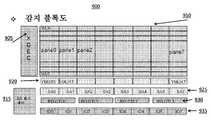
도 11은 플래시 메모리 디바이스(900)를 도시한다. 플래시 메모리 디바이스(900)는: 셀들이 워드 라인들 및 비트 라인들에 의해 액세스되는 메모리 셀들의 어레이(910); 수평 디코더(905); 수직 디코더(920); 판독 펄스 제어 블록(915); 판독 제어 블록들(930); 감지 증폭기 회로 블록들(925); 및 IO 블록들(935)을 포함한다.Figure 11 shows a
판독 제어 블록들(930)은 WL 위치, BL 위치, 및 IO 폭을 추적하는 판독 타이밍 펄스들을 생성하는 데, 그리고 PVT를 보상하는 데 사용된다.Read control blocks 930 are used to generate read timing pulses to track the WL position, BL position, and IO width, and to compensate the PVT.
도 12는 시간에 따른 다양한 제어 신호들의 동작을 보여주는 타이밍도(950)를 도시한다. 신호(951)는 T_SEN-CYC 신호이고, 신호(952)는 T-ATD 신호이고, 신호(953)는 T-PRECHa 신호이고, 신호(954)는 T-EQ 신호이고, 신호(955)는 T-SENSEa 신호이고, 신호(956)는 T-DOLATCH 신호이고, 신호(957)는 T-BL0, BL1 신호이고, 신호(958)는 T-SO0, SO1 신호이며, 신호(959)는 T-SOUT 신호이다.FIG. 12 shows a timing diagram 950 illustrating the operation of various control signals over time.
신호(953)(T-PRECHa)는 적응적 사전 충전 펄스화(adaptive precharge pulsing)를 수행한다. 펄스는 WL0(워드 라인을 따른 위치 0)에서 더 짧고, WL-N(워드 라인을 따른 위치 N)에서 더 길며, 그것은 IO0(IO 라인을 따른 위치 0)에서 더 짧고, IO-N(IO 라인을 따른 위치 N)에서 더 길다. 신호(953)(T-PRECHa)는 WL 지연 및 BL 지연을 추적하며, 예를 들어 그것의 펄스들은 WL0/BL0에 대해 가장 짧다.Signal 953 (T-PRECHa) performs adaptive precharge pulsing. The pulse is shorter at WL0 (
신호(955)(T-SENSAa)는 적응적 감지 펄스화를 수행한다. 펄스는 IO0에서 더 짧고, IO-N에서 더 길다. 펄스는 WL0에서 더 짧고, WL-end에서 더 길다. 그것은 WL 지연 및 BL 지연을 추적하며, 예를 들어 그것의 펄스들은 WL-N/BL-N에 대해 가장 길다.Signal 955 (T-SENSAa) performs adaptive sense pulsing. The pulse is shorter at IOO and longer at IO-N. The pulse is shorter at WL0 and longer at WL-end. It tracks WL delay and BL delay, for example its pulses are longest for WL-N / BL-N.
신호(951)(T-SEN-CYC)는 감지 사이클이 완료된 후에 자동 전력 차단을 수행한다.Signal 951 (T-SEN-CYC) performs automatic power down after the sense cycle is complete.
도 13은 두 개의 그래프들을 도시한다. 제1 그래프는 WL 바이어스가 다른 것보다 비트 라인의 일 단부에서 더 높다는 것을 보여주고, 제2 그래프는 BL 바이어스가 다른 것보다 비트 라인의 일 단부에서 더 높다는 것을 보여준다. 이는 도 9 및 도 10을 참조하여 전술된 바와 같이 비트 라인들 사이의 기생 커패시턴스를 증가시킴이 없이 비트 라인들의 저항을 감소시키는 것의 중요성을 보여준다.Figure 13 shows two graphs. The first graph shows that the WL bias is higher at one end of the bit line than the other, and the second graph shows that the BL bias is higher at one end of the bit line than the other. This shows the importance of reducing the resistance of the bit lines without increasing the parasitic capacitance between the bit lines as described above with reference to Figures 9 and 10. [
본 명세서에서의 본 발명에 대한 언급은 임의의 청구항 또는 청구항 용어의 범주를 제한하려는 것이 아니라, 대신, 청구항들 중 하나 이상에 의해 포괄될 수 있는 하나 이상의 특징들에 대해 언급하는 것일 뿐이다. 전술된 물질들, 프로세스들, 및 수치 예들은 단지 예시적일 뿐이며, 청구범위를 제한하는 것으로 간주되어서는 안 된다. 본 명세서에 사용된 바와 같이, 용어들 "~ 위에" 및 "~ 상에" 둘 모두는 포괄적으로 "~ 상에 직접적으로"(사이에 어떠한 중간의 물질들, 요소들 또는 공간도 배치되지 않음)와 "~ 상에 간접적으로"(사이에 중간의 물질들, 요소들 또는 공간이 배치됨)를 포함한다는 것에 주의하여야 한다. 마찬가지로, 용어 "인접한"은 "직접적으로 인접한"(사이에 어떠한 중간의 물질들, 요소들 또는 공간도 배치되지 않음) 및 "간접적으로 인접한"(사이에 중간의 물질들, 요소들 또는 공간이 배치됨)을 포함한다. 예를 들어, "기판 위에" 요소를 형성하는 것은 어떠한 중간의 물질들/요소들도 사이에 두지 않고 기판 상에 직접적으로 요소를 형성하는 것뿐만 아니라 하나 이상의 중간의 물질들/요소들을 사이에 두어 기판 상에 간접적으로 요소를 형성하는 것을 포함할 수 있다.Reference herein to the present invention is not intended to limit the scope of any claim or claim term, but instead only refers to one or more features that may be encompassed by one or more of the claims. The foregoing materials, processes, and numerical examples are illustrative only and are not to be construed as limiting the scope of the claims. As used herein, the terms "on" and "on" both refer collectively to " directly on "(without any intermediate material, And "indirectly on" (including intermediate materials, elements or spaces disposed between). Likewise, the term "adjacent" means that any intermediate material, element or space is placed between " directly adjacent "(no intermediate materials, elements or spaces disposed between) and" ). For example, forming an "on-substrate" element does not place any intermediate material (s) / element (s) therebetween, but rather creates one or more intermediate materials / And indirectly forming an element on the substrate.
Claims (24)
Translated fromKorean플래시 메모리 셀들에 액세스하기 위한 제1 세트의 비트 라인들을 포함하는 제1 금속 층; 및
플래시 메모리 셀들에 액세스하기 위한 제2 세트의 비트 라인들을 포함하는 제2 금속 층을 포함하는, 플래시 메모리 디바이스.As a flash memory device,
A first metal layer comprising a first set of bit lines for accessing flash memory cells; And
And a second metal layer comprising a second set of bit lines for accessing flash memory cells.
상기 제2 세트의 비트 라인들 중의 각각의 비트 라인은 하나 이상의 비아(via)들에 의해 상기 제1 금속 층에 커플링되는, 플래시 메모리 디바이스.The method according to claim 1,
Wherein each bit line of the second set of bit lines is coupled to the first metal layer by one or more vias.
상기 제1 세트의 비트 라인들 중의 제1 라인과 상기 제1 세트의 비트 라인들 중의 최밀접 비트 라인 사이의 거리는 상기 제1 라인과 상기 제2 세트의 비트 라인들 중의 최밀접 비트 라인 사이의 거리보다 더 큰, 플래시 메모리 디바이스.The method according to claim 1,
Wherein a distance between a first line of the first set of bit lines and a closest bit line of the first set of bit lines is greater than a distance between the first line and a closest bit line of the second set of bit lines Lt; / RTI > device.
플래시 메모리 셀들에 액세스하기 위한 비트 라인들의 세트를 포함하는 제1 금속 층; 및
상기 비트 라인들의 세트에 평행한 복수의 구조물들을 포함하는 제2 금속 층을 포함하고, 상기 복수의 구조물들 중의 각각의 구조물은 상기 비트 라인들의 세트 중의 상이한 비트 라인에 커플링되는, 플래시 메모리 디바이스.As a flash memory device,
A first metal layer comprising a set of bit lines for accessing flash memory cells; And
A second metal layer comprising a plurality of structures parallel to the set of bit lines, wherein each structure of the plurality of structures is coupled to a different bit line in the set of bit lines.
상기 복수의 구조물들 중의 각각의 구조물은 상기 제1 금속 층과 상기 제2 금속 층 사이의 하나 이상의 커넥터들에 의해 상기 비트 라인들의 세트 중의 상이한 비트 라인에 커플링되는, 플래시 메모리 디바이스.The method of claim 4,
Wherein each structure of the plurality of structures is coupled to a different bit line in the set of bit lines by one or more connectors between the first metal layer and the second metal layer.
상기 복수의 구조물들 중의 각각의 구조물은 상기 비트 라인들의 세트 중의 각각의 비트 라인보다 더 짧은, 플래시 메모리 디바이스.The method of claim 5,
Each structure of the plurality of structures being shorter than a respective bit line of the set of bit lines.
상기 복수의 구조물들은 상기 제2 금속 층 내에 엇갈린(stagger) 형태로 배열되는, 플래시 메모리 디바이스.The method of claim 6,
Wherein the plurality of structures are arranged in a staggered fashion within the second metal layer.
선택된 플래시 메모리 셀에 커플링되고, 비트 라인, 제1 인접 비트 라인으로부터의 제1 기생 커패시터, 및 제2 인접 비트 라인으로부터의 제2 기생 커패시터를 포함하는 메모리 데이터 판독 블록;
기준 메모리 셀에 커플링되는 메모리 기준 판독 블록; 및
상기 메모리 데이터 판독 블록 및 상기 메모리 기준 판독 블록에 커플링되어 상기 선택된 플래시 메모리 셀에 저장된 값을 판정하기 위한 차동 증폭기 블록을 포함하고,
상기 메모리 데이터 판독 블록 및 상기 메모리 기준 판독 블록은 사전 충전 회로에 커플링되어 상기 제1 기생 커패시터 및 상기 제2 기생 커패시터를 보상하는, 감지 회로.As a sensing circuit,
A memory data read block coupled to the selected flash memory cell and including a bit line, a first parasitic capacitor from a first adjacent bit line, and a second parasitic capacitor from a second adjacent bit line;
A memory reference read block coupled to the reference memory cell; And
And a differential amplifier block coupled to the memory data read block and the memory reference read block to determine a value stored in the selected flash memory cell,
Wherein the memory data read block and the memory reference read block are coupled to a precharge circuit to compensate for the first parasitic capacitor and the second parasitic capacitor.
상기 메모리 데이터 판독 블록은 전류원, 캐스코딩(cascoding) 감지 NMOS 트랜지스터, 비트 라인 클램프(bitline clamp) NMOS 트랜지스터, 다이오드 접속형 감지 부하(diode connected sensing load) PMOS 트랜지스터, 및 커패시터를 포함하는, 감지 회로.The method of claim 8,
Wherein the memory data read block comprises a current source, a cascoding sensing NMOS transistor, a bitline clamp NMOS transistor, a diode connected sensing load PMOS transistor, and a capacitor.
상기 메모리 기준 판독 블록은 전류원, 기준 비트 라인 클램프 NMOS 트랜지스터, 캐스코딩 감지 NMOS 트랜지스터, 다이오드 접속형 감지 부하 PMOS 트랜지스터, 및 커패시터를 포함하는, 감지 회로.The method of claim 9,
Wherein the memory reference read block comprises a current source, a reference bit line clamp NMOS transistor, a cascading sense NMOS transistor, a diode connected sense load PMOS transistor, and a capacitor.
상기 차동 증폭기 블록은 NMOS 트랜지스터들의 입력 차동 쌍, 전류 미러 부하 PMOS 트랜지스터들, 출력 PMOS 트랜지스터, 전류 바이어스 NMOS 트랜지스터, 및 출력 전류 바이어스 NMOS 트랜지스터를 포함하는, 감지 회로.The method of claim 10,
Wherein the differential amplifier block includes an input differential pair of NMOS transistors, current mirror load PMOS transistors, an output PMOS transistor, a current bias NMOS transistor, and an output current bias NMOS transistor.
선택된 플래시 메모리 셀에 커플링되는 비트 라인;
상기 비트 라인 및 제1 인접 비트 라인에 커플링되는 제1 기생 커패시터;
상기 비트 라인 및 제2 인접 비트 라인에 커플링되는 제2 기생 커패시터;
상기 비트 라인에 커플링되어 상기 비트 라인을 바이어스 전압으로 사전 충전하기 위한 사전 충전 회로; 및
PMOS 트랜지스터 및 NMOS 트랜지스터를 포함하는 싱글 엔디드 증폭기(single ended amplifier)를 포함하고,
상기 PMOS 트랜지스터의 게이트는 상기 비트 라인에 커플링되고, 상기 증폭기의 출력은 상기 선택된 플래시 메모리 셀에 저장된 값을 나타내는, 감지 회로.As a sensing circuit,
A bit line coupled to the selected flash memory cell;
A first parasitic capacitor coupled to the bit line and a first adjacent bit line;
A second parasitic capacitor coupled to the bit line and a second adjacent bit line;
A precharge circuit coupled to the bit line to precharge the bit line to a bias voltage; And
A single ended amplifier comprising a PMOS transistor and an NMOS transistor,
The gate of the PMOS transistor being coupled to the bit line and the output of the amplifier representing a value stored in the selected flash memory cell.
상기 출력은 기준 메모리 셀의 사용 없이 생성되는, 감지 회로.The method of claim 12,
Wherein the output is generated without the use of a reference memory cell.
상기 바이어스 전압은 선택되고 있는 상기 메모리 셀들의 위치를 추적하는, 감지 회로.The method of claim 12,
Wherein the bias voltage tracks the location of the memory cells being selected.
상기 PMOS 트랜지스터의 벌크가 순방향 바이어싱되는, 감지 회로.The method of claim 12,
Wherein the bulk of the PMOS transistor is forward biased.
상기 사전 충전 회로는 상기 비트 라인에 커플링되어 사전 충전 전압을 저장하기 위한 비트 라인 커패시터를 포함하는, 감지 회로.The method of claim 12,
Wherein the precharge circuit is coupled to the bit line to include a bit line capacitor for storing a precharge voltage.
상기 사전 충전 회로는, 전압원 및 상기 비트 라인에 커플링되고 사전 충전 제어 신호에 의해 제어되는 PMOS 트랜지스터를 포함하는, 감지 회로.14. The method of claim 13,
Wherein the precharge circuit comprises a voltage source and a PMOS transistor coupled to the bit line and controlled by a precharge control signal.
상기 사전 충전 전압은 선택되고 있는 상기 메모리 셀들의 위치를 추적하는, 감지 회로.18. The method of claim 16,
Wherein the precharge voltage tracks the location of the memory cells being selected.
상기 사전 충전 제어 신호는 선택되고 있는 상기 메모리 셀들의 위치를 추적하는, 감지 회로.18. The method of claim 17,
Wherein the precharge control signal tracks the location of the memory cells being selected.
플래시 메모리 셀에 커플링되는 선택된 비트 라인;
상기 선택된 비트 라인 및 제1 인접 비트 라인에 커플링되는 제1 기생 커패시터;
상기 비트 라인 및 제2 인접 비트 라인에 커플링되는 제2 기생 커패시터;
기준 메모리 셀에 커플링되는 기준 라인;
상기 기준 라인 및 제3 인접 비트 라인에 커플링되는 제3 기생 커패시터;
상기 기준 라인 및 제4 인접 비트 라인에 커플링되는 제4 기생 커패시터; 및
상기 선택된 비트 라인 및 상기 기준 라인에 커플링되어 상기 선택된 플래시 메모리 셀에 저장된 값을 판정하기 위한 차동 증폭기를 포함하고,
상기 선택된 비트 라인 및 상기 기준 라인은 사전 충전 회로에 커플링되어 상기 제1 기생 커패시터, 상기 제2 기생 커패시터, 상기 제3 기생 커패시터, 및 상기 제4 기생 커패시터를 보상하는, 감지 회로.As a sensing circuit,
A selected bit line coupled to the flash memory cell;
A first parasitic capacitor coupled to the selected bit line and a first adjacent bit line;
A second parasitic capacitor coupled to the bit line and a second adjacent bit line;
A reference line coupled to the reference memory cell;
A third parasitic capacitor coupled to the reference line and a third adjacent bit line;
A fourth parasitic capacitor coupled to the reference line and a fourth adjacent bit line; And
And a differential amplifier coupled to the selected bit line and the reference line to determine a value stored in the selected flash memory cell,
Wherein the selected bit line and the reference line are coupled to a precharge circuit to compensate for the first parasitic capacitor, the second parasitic capacitor, the third parasitic capacitor, and the fourth parasitic capacitor.
상기 사전 충전 회로는 상기 선택된 비트 라인에 커플링되어 사전 충전 전압을 저장하기 위한 비트 라인 커패시터, 및 상기 기준 라인에 커플링되어 사전 충전 전압을 저장하기 위한 기준 라인 커패시터를 포함하는, 감지 회로.The method of claim 20,
Wherein the precharge circuit comprises a bit line capacitor coupled to the selected bit line to store a precharge voltage and a reference line capacitor coupled to the reference line to store a precharge voltage.
상기 사전 충전 회로는, 전압원 및 상기 선택된 비트 라인에 커플링되고 사전 충전 제어 신호에 의해 제어되는 PMOS 트랜지스터를 포함하는, 감지 회로.23. The method of claim 21,
Wherein the precharge circuit comprises a voltage source and a PMOS transistor coupled to the selected bit line and controlled by a precharge control signal.
상기 사전 충전 제어 신호는 선택되고 있는 상기 메모리 셀들의 위치를 추적하는, 감지 회로.23. The method of claim 22,
Wherein the precharge control signal tracks the location of the memory cells being selected.
상기 PMOS 트랜지스터의 벌크가 순방향 바이어싱되는, 감지 회로.23. The method of claim 22,
Wherein the bulk of the PMOS transistor is forward biased.
Applications Claiming Priority (5)
| Application Number | Priority Date | Filing Date | Title |
|---|---|---|---|
| US201361799970P | 2013-03-15 | 2013-03-15 | |
| US61/799,970 | 2013-03-15 | ||
| US13/958,415 | 2013-08-02 | ||
| US13/958,415US20140269061A1 (en) | 2013-03-15 | 2013-08-02 | High Speed Sensing For Advanced Nanometer Flash Memory Device |
| PCT/US2014/011554WO2014149166A1 (en) | 2013-03-15 | 2014-01-14 | High speed sensing for advanced nanometer flash memory device |
Publications (2)
| Publication Number | Publication Date |
|---|---|
| KR20150103708Atrue KR20150103708A (en) | 2015-09-11 |
| KR101691319B1 KR101691319B1 (en) | 2016-12-29 |
Family
ID=51526478
Family Applications (1)
| Application Number | Title | Priority Date | Filing Date |
|---|---|---|---|
| KR1020157020604AActiveKR101691319B1 (en) | 2013-03-15 | 2014-01-14 | High speed sensing for advanced nanometer flash memory device |
Country Status (7)
| Country | Link |
|---|---|
| US (2) | US20140269061A1 (en) |
| EP (2) | EP2973708B1 (en) |
| JP (2) | JP2016514366A (en) |
| KR (1) | KR101691319B1 (en) |
| CN (2) | CN104937718B (en) |
| TW (1) | TWI545697B (en) |
| WO (1) | WO2014149166A1 (en) |
Families Citing this family (10)
| Publication number | Priority date | Publication date | Assignee | Title |
|---|---|---|---|---|
| CN106782649B (en)* | 2015-11-20 | 2020-07-14 | 华邦电子股份有限公司 | Sense amplifier circuit |
| CN106935267B (en)* | 2015-12-31 | 2020-11-10 | 硅存储技术公司 | Low power sense amplifier for flash memory system |
| US10149377B2 (en) | 2016-06-24 | 2018-12-04 | Invensas Corporation | Stacked transmission line |
| CN110610738B (en)* | 2018-06-15 | 2023-08-18 | 硅存储技术公司 | Improved sense amplifier for flash memory systems |
| JP2020102290A (en) | 2018-12-21 | 2020-07-02 | キオクシア株式会社 | Semiconductor memory device |
| CN110704332B (en)* | 2019-08-29 | 2021-11-09 | 深圳大普微电子科技有限公司 | Flash memory medium optimization method and nonvolatile storage device |
| CN111758171B (en)* | 2020-05-12 | 2024-04-05 | 长江先进存储产业创新中心有限责任公司 | Novel distributed array and contact architecture for 4-stacked 3D PCM memory |
| US20210397937A1 (en)* | 2020-06-22 | 2021-12-23 | Qualcomm Incorporated | Charge-pump-based current-mode neuron for machine learning |
| CN114171083B (en)* | 2020-11-03 | 2025-05-06 | 台湾积体电路制造股份有限公司 | Memory Devices |
| CN117015229A (en)* | 2022-04-26 | 2023-11-07 | 长鑫存储技术有限公司 | Three-dimensional memory and forming method thereof |
Citations (3)
| Publication number | Priority date | Publication date | Assignee | Title |
|---|---|---|---|---|
| KR100276536B1 (en)* | 1995-02-10 | 2001-01-15 | 로데릭 더블류 루이스 | Fast-sensing amplifier for flash memory |
| KR20100033192A (en)* | 2008-09-19 | 2010-03-29 | 삼성전자주식회사 | Flash memory device and systems and reading methods thereof |
| KR20110056005A (en)* | 2009-11-20 | 2011-05-26 | 삼성전자주식회사 | Wiring Structure of Semiconductor Device |
Family Cites Families (34)
| Publication number | Priority date | Publication date | Assignee | Title |
|---|---|---|---|---|
| JPH06195990A (en)* | 1992-12-21 | 1994-07-15 | Kawasaki Steel Corp | Semiconductor memory device |
| US6108237A (en)* | 1997-07-17 | 2000-08-22 | Micron Technology, Inc. | Fast-sensing amplifier for flash memory |
| DE69702256T2 (en)* | 1996-06-24 | 2001-01-18 | Advanced Micro Devices, Inc. | METHOD FOR A MULTIPLE, BITS PER CELL FLASH EEPROM, MEMORY WITH SIDE PROGRAMMING MODE, AND READING METHOD |
| JPH11134891A (en)* | 1997-10-31 | 1999-05-21 | Sanyo Electric Co Ltd | Semiconductor memory device |
| JP2002057227A (en)* | 2000-08-11 | 2002-02-22 | Mitsubishi Electric Corp | Semiconductor storage device |
| JP2004111478A (en)* | 2002-09-13 | 2004-04-08 | Sharp Corp | Nonvolatile semiconductor memory device and method of manufacturing the same |
| JP2004119457A (en)* | 2002-09-24 | 2004-04-15 | Matsushita Electric Ind Co Ltd | Semiconductor storage device |
| JP4012144B2 (en)* | 2003-12-25 | 2007-11-21 | 株式会社東芝 | Semiconductor memory device |
| US7177176B2 (en)* | 2004-06-30 | 2007-02-13 | Intel Corporation | Six-transistor (6T) static random access memory (SRAM) with dynamically variable p-channel metal oxide semiconductor (PMOS) strength |
| CN101203919A (en)* | 2005-03-04 | 2008-06-18 | 爱特梅尔公司 | Fast read port for register file |
| KR100632656B1 (en)* | 2005-05-23 | 2006-10-11 | 주식회사 하이닉스반도체 | Bit line formation method of flash memory device |
| CN100395843C (en)* | 2005-06-02 | 2008-06-18 | 复旦大学 | High Speed Low Power Current Sense Amplifier |
| KR100675517B1 (en)* | 2005-09-09 | 2007-01-30 | 주식회사 엑셀반도체 | Serial Flash Memory Device and Precharge Method |
| JP2007080424A (en)* | 2005-09-15 | 2007-03-29 | Renesas Technology Corp | Nonvolatile memory |
| US7638878B2 (en)* | 2006-04-13 | 2009-12-29 | Micron Technology, Inc. | Devices and systems including the bit lines and bit line contacts |
| JP2008047189A (en)* | 2006-08-11 | 2008-02-28 | Matsushita Electric Ind Co Ltd | Semiconductor memory device |
| US7675783B2 (en)* | 2007-02-27 | 2010-03-09 | Samsung Electronics Co., Ltd. | Nonvolatile memory device and driving method thereof |
| JP4504397B2 (en)* | 2007-05-29 | 2010-07-14 | 株式会社東芝 | Semiconductor memory device |
| JP2009016016A (en)* | 2007-07-09 | 2009-01-22 | Samsung Electronics Co Ltd | Semiconductor integrated circuit |
| US7755962B2 (en)* | 2007-07-09 | 2010-07-13 | Samsung Electronics Co., Ltd. | Semiconductor memory devices, memory systems and computing systems including the same |
| US7697365B2 (en)* | 2007-07-13 | 2010-04-13 | Silicon Storage Technology, Inc. | Sub volt flash memory system |
| US7977709B2 (en)* | 2008-01-02 | 2011-07-12 | Infineon Technologies Ag | MOS transistor and semiconductor device |
| TWI398874B (en)* | 2008-03-17 | 2013-06-11 | Elpida Memory Inc | Semiconductor device having single-ended sensing amplifier |
| US8018773B2 (en) | 2009-03-04 | 2011-09-13 | Silicon Storage Technology, Inc. | Array of non-volatile memory cells including embedded local and global reference cells and system |
| CN102081959B (en)* | 2009-11-26 | 2013-06-12 | 中国科学院微电子研究所 | Memory reading circuit and memory |
| JP2011138569A (en)* | 2009-12-25 | 2011-07-14 | Toshiba Corp | Nonvolatile semiconductor memory device |
| US8385147B2 (en)* | 2010-03-30 | 2013-02-26 | Silicon Storage Technology, Inc. | Systems and methods of non-volatile memory sensing including selective/differential threshold voltage features |
| US8274828B2 (en)* | 2010-12-15 | 2012-09-25 | Fs Semiconductor Corp., Ltd. | Structures and methods for reading out non-volatile memory using referencing cells |
| JP4982606B2 (en)* | 2010-12-22 | 2012-07-25 | 株式会社東芝 | Semiconductor memory device and control method thereof |
| US8605521B2 (en)* | 2011-05-12 | 2013-12-10 | Micron Technology, Inc. | Sense amplifiers, memories, and apparatuses and methods for sensing a data state of a memory cell |
| US8320211B1 (en)* | 2011-05-16 | 2012-11-27 | National Tsing Hua University | Current-sense amplifier with low-offset adjustment and method of low-offset adjustment thereof |
| CN202534357U (en)* | 2012-03-19 | 2012-11-14 | 河南科技大学 | Current type sensitive amplifier used for ferroelectric ram memorizer reading circuit |
| KR101916192B1 (en)* | 2012-04-19 | 2018-11-07 | 삼성전자주식회사 | Nonvolatile memory device comprising flag cell and user device comprising the same |
| US8928406B2 (en)* | 2013-03-13 | 2015-01-06 | Texas Instruments Incorporated | Low-power inverter-based differential amplifier |
- 2013
- 2013-08-02USUS13/958,415patent/US20140269061A1/ennot_activeAbandoned
- 2014
- 2014-01-14CNCN201480005640.XApatent/CN104937718B/enactiveActive
- 2014-01-14EPEP14702703.1Apatent/EP2973708B1/enactiveActive
- 2014-01-14JPJP2015560182Apatent/JP2016514366A/enactivePending
- 2014-01-14WOPCT/US2014/011554patent/WO2014149166A1/enactiveApplication Filing
- 2014-01-14EPEP17181079.9Apatent/EP3264416A3/ennot_activeCeased
- 2014-01-14CNCN201810146062.1Apatent/CN108198581B/enactiveActive
- 2014-01-14KRKR1020157020604Apatent/KR101691319B1/enactiveActive
- 2014-01-21TWTW103102093Apatent/TWI545697B/enactive
- 2017
- 2017-10-24USUS15/792,590patent/US10283206B2/enactiveActive
- 2018
- 2018-01-16JPJP2018004736Apatent/JP6676081B2/enactiveActive
Patent Citations (3)
| Publication number | Priority date | Publication date | Assignee | Title |
|---|---|---|---|---|
| KR100276536B1 (en)* | 1995-02-10 | 2001-01-15 | 로데릭 더블류 루이스 | Fast-sensing amplifier for flash memory |
| KR20100033192A (en)* | 2008-09-19 | 2010-03-29 | 삼성전자주식회사 | Flash memory device and systems and reading methods thereof |
| KR20110056005A (en)* | 2009-11-20 | 2011-05-26 | 삼성전자주식회사 | Wiring Structure of Semiconductor Device |
Also Published As
| Publication number | Publication date |
|---|---|
| EP3264416A2 (en) | 2018-01-03 |
| US10283206B2 (en) | 2019-05-07 |
| EP2973708B1 (en) | 2017-10-18 |
| JP2016514366A (en) | 2016-05-19 |
| WO2014149166A1 (en) | 2014-09-25 |
| TWI545697B (en) | 2016-08-11 |
| KR101691319B1 (en) | 2016-12-29 |
| US20140269061A1 (en) | 2014-09-18 |
| CN108198581A (en) | 2018-06-22 |
| CN104937718B (en) | 2018-03-06 |
| CN108198581B (en) | 2023-04-07 |
| US20180047454A1 (en) | 2018-02-15 |
| JP6676081B2 (en) | 2020-04-08 |
| CN104937718A (en) | 2015-09-23 |
| EP2973708A1 (en) | 2016-01-20 |
| TW201440174A (en) | 2014-10-16 |
| EP3264416A3 (en) | 2018-04-04 |
| JP2018101457A (en) | 2018-06-28 |
Similar Documents
| Publication | Publication Date | Title |
|---|---|---|
| KR101691319B1 (en) | High speed sensing for advanced nanometer flash memory device | |
| US8792269B1 (en) | Fast programming of magnetic random access memory (MRAM) | |
| US8067792B2 (en) | Memory device with memory cell including MuGFET and FIN capacitor | |
| US9355709B2 (en) | Digit line equilibration using access devices at the edge of sub-arrays | |
| TW201503140A (en) | Friendly lithography partial reading circuit for reverse gate flash memory device and manufacturing method thereof | |
| US20150318043A1 (en) | Method For Defining A Default State of a Charge Trap Based Memory Cell | |
| US9858977B1 (en) | Programming of magnetic random access memory (MRAM) by boosting gate voltage | |
| KR100745902B1 (en) | Nonvolatile Ferroelectric Memory Devices | |
| KR100682212B1 (en) | Nonvolatile Ferroelectric Memory Devices | |
| JP2023179834A (en) | semiconductor equipment | |
| KR100636925B1 (en) | Nonvolatile Ferroelectric Memory Devices | |
| TWI497524B (en) | Memory page buffer | |
| JP2003331590A (en) | Nonvolatile semiconductor memory device | |
| JP2006196113A (en) | Nonvolatile semiconductor memory device | |
| KR20080022268A (en) | Single chip memory device integrated sram and non-volatile memory using bitline sharing |
Legal Events
| Date | Code | Title | Description |
|---|---|---|---|
| A201 | Request for examination | ||
| PA0105 | International application | Patent event date:20150729 Patent event code:PA01051R01D Comment text:International Patent Application | |
| PA0201 | Request for examination | ||
| PG1501 | Laying open of application | ||
| E902 | Notification of reason for refusal | ||
| PE0902 | Notice of grounds for rejection | Comment text:Notification of reason for refusal Patent event date:20160729 Patent event code:PE09021S01D | |
| E701 | Decision to grant or registration of patent right | ||
| PE0701 | Decision of registration | Patent event code:PE07011S01D Comment text:Decision to Grant Registration Patent event date:20161121 | |
| GRNT | Written decision to grant | ||
| PR0701 | Registration of establishment | Comment text:Registration of Establishment Patent event date:20161223 Patent event code:PR07011E01D | |
| PR1002 | Payment of registration fee | Payment date:20161223 End annual number:3 Start annual number:1 | |
| PG1601 | Publication of registration | ||
| PR1001 | Payment of annual fee | Payment date:20201201 Start annual number:5 End annual number:5 | |
| PR1001 | Payment of annual fee | Payment date:20211122 Start annual number:6 End annual number:6 | |
| PR1001 | Payment of annual fee | Payment date:20221123 Start annual number:7 End annual number:7 | |
| PR1001 | Payment of annual fee | Payment date:20231128 Start annual number:8 End annual number:8 |