KR20150094856A - Display device and method of manufacturing display device using the same - Google Patents
Display device and method of manufacturing display device using the sameDownload PDFInfo
- Publication number
- KR20150094856A KR20150094856AKR1020140015334AKR20140015334AKR20150094856AKR 20150094856 AKR20150094856 AKR 20150094856AKR 1020140015334 AKR1020140015334 AKR 1020140015334AKR 20140015334 AKR20140015334 AKR 20140015334AKR 20150094856 AKR20150094856 AKR 20150094856A
- Authority
- KR
- South Korea
- Prior art keywords
- light
- width
- insulating layer
- contact hole
- translucent
- Prior art date
- Legal status (The legal status is an assumption and is not a legal conclusion. Google has not performed a legal analysis and makes no representation as to the accuracy of the status listed.)
- Granted
Links
- 238000004519manufacturing processMethods0.000titledescription6
- 239000000758substrateSubstances0.000claimsabstractdescription23
- 239000010409thin filmSubstances0.000claimsabstractdescription9
- 238000000034methodMethods0.000claimsdescription28
- 239000004065semiconductorSubstances0.000claimsdescription18
- 239000010408filmSubstances0.000description14
- 230000000903blocking effectEffects0.000description13
- 230000010363phase shiftEffects0.000description11
- 239000000463materialSubstances0.000description9
- 229910044991metal oxideInorganic materials0.000description8
- 150000004706metal oxidesChemical class0.000description8
- VYPSYNLAJGMNEJ-UHFFFAOYSA-Nsilicon dioxideInorganic materialsO=[Si]=OVYPSYNLAJGMNEJ-UHFFFAOYSA-N0.000description8
- 238000002834transmittanceMethods0.000description7
- 229910007541Zn OInorganic materials0.000description6
- 229910045601alloyInorganic materials0.000description6
- 239000000956alloySubstances0.000description6
- 230000001681protective effectEffects0.000description6
- 239000004973liquid crystal related substanceSubstances0.000description5
- ZOKXTWBITQBERF-UHFFFAOYSA-NMolybdenumChemical compound[Mo]ZOKXTWBITQBERF-UHFFFAOYSA-N0.000description4
- 229910021417amorphous siliconInorganic materials0.000description4
- 239000011651chromiumSubstances0.000description4
- 229910052750molybdenumInorganic materials0.000description4
- 239000011733molybdenumSubstances0.000description4
- 238000007789sealingMethods0.000description4
- VYZAMTAEIAYCRO-UHFFFAOYSA-NChromiumChemical compound[Cr]VYZAMTAEIAYCRO-UHFFFAOYSA-N0.000description3
- GYHNNYVSQQEPJS-UHFFFAOYSA-NGalliumChemical compound[Ga]GYHNNYVSQQEPJS-UHFFFAOYSA-N0.000description3
- 229910052782aluminiumInorganic materials0.000description3
- XAGFODPZIPBFFR-UHFFFAOYSA-NaluminiumChemical compound[Al]XAGFODPZIPBFFR-UHFFFAOYSA-N0.000description3
- 229910052804chromiumInorganic materials0.000description3
- 239000012141concentrateSubstances0.000description3
- 230000005684electric fieldEffects0.000description3
- 229910052733galliumInorganic materials0.000description3
- 229910052738indiumInorganic materials0.000description3
- APFVFJFRJDLVQX-UHFFFAOYSA-Nindium atomChemical compound[In]APFVFJFRJDLVQX-UHFFFAOYSA-N0.000description3
- 239000011810insulating materialSubstances0.000description3
- 230000003287optical effectEffects0.000description3
- 239000010453quartzSubstances0.000description3
- 229920005989resinPolymers0.000description3
- 239000011347resinSubstances0.000description3
- 229910052814silicon oxideInorganic materials0.000description3
- JBQYATWDVHIOAR-UHFFFAOYSA-NtellanylidenegermaniumChemical compound[Te]=[Ge]JBQYATWDVHIOAR-UHFFFAOYSA-N0.000description3
- IJGRMHOSHXDMSA-UHFFFAOYSA-NAtomic nitrogenChemical compoundN#NIJGRMHOSHXDMSA-UHFFFAOYSA-N0.000description2
- 229910004205SiNXInorganic materials0.000description2
- ATJFFYVFTNAWJD-UHFFFAOYSA-NTinChemical compound[Sn]ATJFFYVFTNAWJD-UHFFFAOYSA-N0.000description2
- XLOMVQKBTHCTTD-UHFFFAOYSA-NZinc monoxideChemical compound[Zn]=OXLOMVQKBTHCTTD-UHFFFAOYSA-N0.000description2
- QVGXLLKOCUKJST-UHFFFAOYSA-Natomic oxygenChemical compound[O]QVGXLLKOCUKJST-UHFFFAOYSA-N0.000description2
- 239000003990capacitorSubstances0.000description2
- 230000001066destructive effectEffects0.000description2
- BCCOBQSFUDVTJQ-UHFFFAOYSA-NoctafluorocyclobutaneChemical compoundFC1(F)C(F)(F)C(F)(F)C1(F)FBCCOBQSFUDVTJQ-UHFFFAOYSA-N0.000description2
- 235000019407octafluorocyclobutaneNutrition0.000description2
- 229910052760oxygenInorganic materials0.000description2
- 239000001301oxygenSubstances0.000description2
- OKTJSMMVPCPJKN-UHFFFAOYSA-NCarbonChemical compound[C]OKTJSMMVPCPJKN-UHFFFAOYSA-N0.000description1
- OAICVXFJPJFONN-UHFFFAOYSA-NPhosphorusChemical compound[P]OAICVXFJPJFONN-UHFFFAOYSA-N0.000description1
- 239000004642PolyimideSubstances0.000description1
- 229910052581Si3N4Inorganic materials0.000description1
- 229910020923Sn-OInorganic materials0.000description1
- RTAQQCXQSZGOHL-UHFFFAOYSA-NTitaniumChemical compound[Ti]RTAQQCXQSZGOHL-UHFFFAOYSA-N0.000description1
- 229910007604Zn—Sn—OInorganic materials0.000description1
- -1acrylChemical group0.000description1
- 238000007792additionMethods0.000description1
- UMIVXZPTRXBADB-UHFFFAOYSA-NbenzocyclobuteneChemical compoundC1=CC=C2CCC2=C1UMIVXZPTRXBADB-UHFFFAOYSA-N0.000description1
- 230000005540biological transmissionEffects0.000description1
- YXTPWUNVHCYOSP-UHFFFAOYSA-Nbis($l^{2}-silanylidene)molybdenumChemical compound[Si]=[Mo]=[Si]YXTPWUNVHCYOSP-UHFFFAOYSA-N0.000description1
- 229910052799carbonInorganic materials0.000description1
- 238000005229chemical vapour depositionMethods0.000description1
- 239000004020conductorSubstances0.000description1
- 230000007547defectEffects0.000description1
- 238000000151depositionMethods0.000description1
- 230000000694effectsEffects0.000description1
- 239000003822epoxy resinSubstances0.000description1
- 238000005530etchingMethods0.000description1
- 239000011521glassSubstances0.000description1
- 239000012535impuritySubstances0.000description1
- 229910010272inorganic materialInorganic materials0.000description1
- 239000011147inorganic materialSubstances0.000description1
- 230000010354integrationEffects0.000description1
- 229910052751metalInorganic materials0.000description1
- 239000002184metalSubstances0.000description1
- 238000012986modificationMethods0.000description1
- 230000004048modificationEffects0.000description1
- 229910021344molybdenum silicideInorganic materials0.000description1
- 229910052757nitrogenInorganic materials0.000description1
- 150000002894organic compoundsChemical class0.000description1
- KYKLWYKWCAYAJY-UHFFFAOYSA-Noxotin;zincChemical compound[Zn].[Sn]=OKYKLWYKWCAYAJY-UHFFFAOYSA-N0.000description1
- 238000002161passivationMethods0.000description1
- 229910052698phosphorusInorganic materials0.000description1
- 239000011574phosphorusSubstances0.000description1
- 238000000623plasma-assisted chemical vapour depositionMethods0.000description1
- 239000004033plasticSubstances0.000description1
- 229920000058polyacrylatePolymers0.000description1
- 229910021420polycrystalline siliconInorganic materials0.000description1
- 229920000647polyepoxidePolymers0.000description1
- 229920001721polyimidePolymers0.000description1
- 229920005591polysiliconPolymers0.000description1
- 239000003870refractory metalSubstances0.000description1
- 229910021332silicideInorganic materials0.000description1
- FVBUAEGBCNSCDD-UHFFFAOYSA-Nsilicide(4-)Chemical compound[Si-4]FVBUAEGBCNSCDD-UHFFFAOYSA-N0.000description1
- 239000000377silicon dioxideSubstances0.000description1
- HQVNEWCFYHHQES-UHFFFAOYSA-Nsilicon nitrideChemical compoundN12[Si]34N5[Si]62N3[Si]51N64HQVNEWCFYHHQES-UHFFFAOYSA-N0.000description1
- 229910052709silverInorganic materials0.000description1
- 239000004332silverSubstances0.000description1
- 229910052715tantalumInorganic materials0.000description1
- GUVRBAGPIYLISA-UHFFFAOYSA-Ntantalum atomChemical compound[Ta]GUVRBAGPIYLISA-UHFFFAOYSA-N0.000description1
- 229920001187thermosetting polymerPolymers0.000description1
- 229910052719titaniumInorganic materials0.000description1
- 239000010936titaniumSubstances0.000description1
- YVTHLONGBIQYBO-UHFFFAOYSA-Nzinc indium(3+) oxygen(2-)Chemical compound[O--].[Zn++].[In+3]YVTHLONGBIQYBO-UHFFFAOYSA-N0.000description1
- 239000011787zinc oxideSubstances0.000description1
Images


Classifications
- G—PHYSICS
- G03—PHOTOGRAPHY; CINEMATOGRAPHY; ANALOGOUS TECHNIQUES USING WAVES OTHER THAN OPTICAL WAVES; ELECTROGRAPHY; HOLOGRAPHY
- G03F—PHOTOMECHANICAL PRODUCTION OF TEXTURED OR PATTERNED SURFACES, e.g. FOR PRINTING, FOR PROCESSING OF SEMICONDUCTOR DEVICES; MATERIALS THEREFOR; ORIGINALS THEREFOR; APPARATUS SPECIALLY ADAPTED THEREFOR
- G03F1/00—Originals for photomechanical production of textured or patterned surfaces, e.g., masks, photo-masks, reticles; Mask blanks or pellicles therefor; Containers specially adapted therefor; Preparation thereof
- G03F1/26—Phase shift masks [PSM]; PSM blanks; Preparation thereof
- G03F1/32—Attenuating PSM [att-PSM], e.g. halftone PSM or PSM having semi-transparent phase shift portion; Preparation thereof
- H—ELECTRICITY
- H10—SEMICONDUCTOR DEVICES; ELECTRIC SOLID-STATE DEVICES NOT OTHERWISE PROVIDED FOR
- H10D—INORGANIC ELECTRIC SEMICONDUCTOR DEVICES
- H10D86/00—Integrated devices formed in or on insulating or conducting substrates, e.g. formed in silicon-on-insulator [SOI] substrates or on stainless steel or glass substrates
- H10D86/01—Manufacture or treatment
- H10D86/021—Manufacture or treatment of multiple TFTs
- H10D86/0231—Manufacture or treatment of multiple TFTs using masks, e.g. half-tone masks
- H—ELECTRICITY
- H10—SEMICONDUCTOR DEVICES; ELECTRIC SOLID-STATE DEVICES NOT OTHERWISE PROVIDED FOR
- H10D—INORGANIC ELECTRIC SEMICONDUCTOR DEVICES
- H10D86/00—Integrated devices formed in or on insulating or conducting substrates, e.g. formed in silicon-on-insulator [SOI] substrates or on stainless steel or glass substrates
- H10D86/40—Integrated devices formed in or on insulating or conducting substrates, e.g. formed in silicon-on-insulator [SOI] substrates or on stainless steel or glass substrates characterised by multiple TFTs
- H10D86/441—Interconnections, e.g. scanning lines
- H—ELECTRICITY
- H10—SEMICONDUCTOR DEVICES; ELECTRIC SOLID-STATE DEVICES NOT OTHERWISE PROVIDED FOR
- H10D—INORGANIC ELECTRIC SEMICONDUCTOR DEVICES
- H10D86/00—Integrated devices formed in or on insulating or conducting substrates, e.g. formed in silicon-on-insulator [SOI] substrates or on stainless steel or glass substrates
- H10D86/40—Integrated devices formed in or on insulating or conducting substrates, e.g. formed in silicon-on-insulator [SOI] substrates or on stainless steel or glass substrates characterised by multiple TFTs
- H10D86/451—Integrated devices formed in or on insulating or conducting substrates, e.g. formed in silicon-on-insulator [SOI] substrates or on stainless steel or glass substrates characterised by multiple TFTs characterised by the compositions or shapes of the interlayer dielectrics
- H—ELECTRICITY
- H10—SEMICONDUCTOR DEVICES; ELECTRIC SOLID-STATE DEVICES NOT OTHERWISE PROVIDED FOR
- H10D—INORGANIC ELECTRIC SEMICONDUCTOR DEVICES
- H10D86/00—Integrated devices formed in or on insulating or conducting substrates, e.g. formed in silicon-on-insulator [SOI] substrates or on stainless steel or glass substrates
- H10D86/40—Integrated devices formed in or on insulating or conducting substrates, e.g. formed in silicon-on-insulator [SOI] substrates or on stainless steel or glass substrates characterised by multiple TFTs
- H10D86/60—Integrated devices formed in or on insulating or conducting substrates, e.g. formed in silicon-on-insulator [SOI] substrates or on stainless steel or glass substrates characterised by multiple TFTs wherein the TFTs are in active matrices
- H—ELECTRICITY
- H10—SEMICONDUCTOR DEVICES; ELECTRIC SOLID-STATE DEVICES NOT OTHERWISE PROVIDED FOR
- H10D—INORGANIC ELECTRIC SEMICONDUCTOR DEVICES
- H10D30/00—Field-effect transistors [FET]
- H10D30/60—Insulated-gate field-effect transistors [IGFET]
- H10D30/67—Thin-film transistors [TFT]
- H10D30/674—Thin-film transistors [TFT] characterised by the active materials
- H10D30/6755—Oxide semiconductors, e.g. zinc oxide, copper aluminium oxide or cadmium stannate
Landscapes
- Physics & Mathematics (AREA)
- General Physics & Mathematics (AREA)
- Engineering & Computer Science (AREA)
- Electroluminescent Light Sources (AREA)
- Chemical & Material Sciences (AREA)
- Inorganic Chemistry (AREA)
- Preparing Plates And Mask In Photomechanical Process (AREA)
- Condensed Matter Physics & Semiconductors (AREA)
- Manufacturing & Machinery (AREA)
- Computer Hardware Design (AREA)
- Microelectronics & Electronic Packaging (AREA)
- Power Engineering (AREA)
- Exposure And Positioning Against Photoresist Photosensitive Materials (AREA)
Abstract
Translated fromKoreanDescription
Translated fromKorean본 발명은 표시장치 및 그 제조방법에 관한 것으로, 보다 상세하게는 투광부를 둘러싸는 차광부 및 반투광부를 포함하는 노광 마스크를 이용하여 접촉 구멍이 형성된 표시장치 및 그 제조방법에 관한 것이다.BACKGROUND OF THE INVENTION 1. Field of the Invention The present invention relates to a display device and a method of manufacturing the same, and more particularly to a display device in which a contact hole is formed by using an exposure mask including a light-shielding portion and a semi-light-
일반적으로 액정 표시 장치나 유기 발광 표시 장치 등의 평판 표시 장치는 복수 쌍의 전기장 생성 전극과 그 사이에 들어 있는 전기광학(electro-optical) 활성층을 포함한다. 액정 표시 장치의 경우 전기 광학 활성층으로 액정층을 포함하고, 유기 발광 표시 장치의 경우 전기 광학 활성층으로 유기 발광층을 포함한다.In general, a flat panel display such as a liquid crystal display or an organic light emitting display includes a plurality of pairs of electric field generating electrodes and an electro-optical active layer interposed therebetween. In the case of a liquid crystal display device, a liquid crystal layer is included as an electro-optical active layer, and an organic light emitting layer is included as an electro-optical active layer in an organic light emitting display device.
한 쌍을 이루는 전기장 생성 전극 중 하나는 통상 스위칭 소자에 연결되어 전기 신호를 인가 받고, 전기 광학 활성층은 이 전기 신호를 광학 신호를 변환함으로써 영상이 표시된다.One of the pair of electric field generating electrodes is usually connected to a switching element to receive an electric signal, and the electro-optic active layer converts the electric signal into an optical signal to display an image.
최근 표시장치가 대면적화, 고집적화 되어 감에 따라, 미세 패턴을 형성하기 위한 위상반전 마스크가 사용되고 있다. 바이너리(binary) 마스크에 비해 위상반전(Phase shift) 마스크는 전체 광 투과량을 감소시키는 반면, 미세한 영역에 노광량을 집중시킬 수 있다. 위상반전 마스크는 높은 해상도 관련 수치인 ILS(Image log slope)값을 가져, 해상도를 높일 수 있다. 이에 따라, 표시기판에 형성된 접촉 구멍의 경사면이 높은 기울기를 가지게 되어, 공정 마진이 개선된다.Recently, as the display device becomes larger in size and higher in integration, a phase inversion mask for forming a fine pattern is used. Compared to a binary mask, a phase shift mask can reduce the total light transmission while concentrating the exposure dose in a fine area. The phase inversion mask has an ILS (Image log slope) value, which is a high resolution related value, to increase the resolution. As a result, the inclined surface of the contact hole formed in the display substrate has a high inclination, and the process margin is improved.
그러나, 위상반전 마스크 적용할 경우, 전체 광 투과량이 줄어들어, 최대 광세기(Imax)도 같이 낮아지므로, 패턴 불량이 일어날 가능성이 높아지고, 접촉 구멍과 인접한 절연층이 돌출되고, 접촉 구멍이 형성되지 않는 절연층이 일부 식각된다.However, in the case of applying a phase inversion mask, the total light transmittance is reduced and the maximum light intensity Imax is also lowered, so that the possibility of pattern failure increases, The insulating layer is partially etched.
본 발명의 일 실시예는 표시장치 및 그 제조방법을 제공하고자 한다. 이를 위하여 본 발명의 일 실시예는 투광부를 둘러싸는 차광부 및 반투광부를 포함하는 노광 마스크를 이용하여 접촉 구멍을 형성함으로써 해상도 및 공정 마진을 개선한 표시장치 및 그 제조방법을 제공한다.An embodiment of the present invention is to provide a display device and a method of manufacturing the same. To this end, an embodiment of the present invention provides a display device in which a contact hole is formed by using an exposure mask including a light-shielding portion and a semitransparent portion surrounding a light-transmitting portion, thereby improving resolution and process margin and a method of manufacturing the same.
본 발명의 일 실시예는 기판; 상기 기판 상에 배치된 게이트 배선 및 데이터 배선; 상기 기판 상에 형성되며, 상기 게이트 배선 및 데이터 배선과 연결된 박막 트랜지스터; 상기 박막 트랜지스터와 연결된 화소전극; 및 상기 기판 상에 배치된 절연층을 포함하고, 상기 절연층은 접촉 구멍을 구비하고, 상기 접촉 구멍에서 절연층은 60도 내지 90도의 테이퍼각을 갖는 표시장치를 제공한다.One embodiment of the present invention provides a semiconductor device comprising: a substrate; A gate wiring and a data wiring disposed on the substrate; A thin film transistor formed on the substrate and connected to the gate wiring and the data wiring; A pixel electrode connected to the thin film transistor; And an insulating layer disposed on the substrate, wherein the insulating layer has a contact hole, and the insulating layer in the contact hole has a taper angle of 60 to 90 degrees.
본 발명의 일 실시예에 따르면, 상기 절연층은 반도체층, 드레인 전극, 게이트 배선, 데이터 배선 및 패드 전극 중 적어도 하나를 덮을 수 있다.According to an embodiment of the present invention, the insulating layer may cover at least one of a semiconductor layer, a drain electrode, a gate wire, a data wire, and a pad electrode.
본 발명의 일 실시예에 따르면, 상기 접촉 구멍은 반도체층, 드레인 전극, 게이트 배선, 데이터 배선 및 패드 전극 중 어느 하나를 노출시킬 수 있다.According to an embodiment of the present invention, the contact hole may expose any one of a semiconductor layer, a drain electrode, a gate wire, a data wire, and a pad electrode.
본 발명의 일 실시예는 투광부; 상기 투광부를 둘러싸는 제1 차광부; 상기 제1 차광부를 둘러싸는 반투광부; 및 상기 반투광부를 둘러싸는 제2 차광부;를 포함하는 노광 마스크를 제공한다.According to an embodiment of the present invention, A first light-shielding portion surrounding the light-transmitting portion; A semi-transmissive portion surrounding the first light-shielding portion; And a second light-shielding portion surrounding the semi-light-projecting portion.
본 발명의 일 실시예에 따르면, 상기 제1 차광부와 상기 반투광부는 서로 다른 폭을 가질 수 있다.According to an embodiment of the present invention, the first light-shielding portion and the semi-light-transmitting portion may have different widths.
본 발명의 일 실시예에 따르면, 상기 투광부는 원형 또는 다각형 형상일 수 있다.According to an embodiment of the present invention, the light transmitting portion may have a circular or polygonal shape.
본 발명의 일 실시예에 따르면, 상기 투광부는 접촉 구멍 형성용 패턴일 수 있다.According to an embodiment of the present invention, the light transmitting portion may be a pattern for forming a contact hole.
본 발명의 일 실시예에 따르면, 상기 제1 차광부와 상기 반투광부는 1:0.9 내지 1:2.25의 폭비율을 가질 수 있다.According to an embodiment of the present invention, the first light-shielding portion and the semi-light-transmitting portion may have a width ratio of 1: 0.9 to 1: 2.25.
본 발명의 일 실시예에 따르면, 상기 제1 차광부는 0.1μm 내지 1 μm의 폭을 가질 수 있다.According to an embodiment of the present invention, the first light shielding portion may have a width of 0.1 mu m to 1 mu m.
본 발명의 일 실시예에 따르면, 상기 반투광부는 0.1μm 내지 5 μm의 폭을 가질 수 있다.According to an embodiment of the present invention, the translucent portion may have a width of 0.1 to 5 μm.
본 발명의 일 실시예는 기판 상에 절연층을 형성하는 단계; 노광 마스크를 이용하여 상기 절연층을 노광시키는 단계; 및 노광된 상기 절연층을 현상하여 접촉 구멍을 형성하는 단계;를 포함하고, 상기 노광 마스크는, 투광부; 상기 투광부를 둘러싸는 제1 차광부; 상기 제1 차광부를 둘러싸는 반투광부; 및 상기 반투광부를 둘러싸는 제2 차광부;를 포함하는 표시장치의 제조방법을 제공한다.One embodiment of the present invention provides a method of manufacturing a semiconductor device, comprising: forming an insulating layer on a substrate; Exposing the insulating layer using an exposure mask; And developing the exposed insulating layer to form a contact hole, wherein the exposure mask comprises: a transparent portion; A first light-shielding portion surrounding the light-transmitting portion; A semi-transmissive portion surrounding the first light-shielding portion; And a second light-shielding portion surrounding the semi-light-projecting portion.
본 발명의 일 실시예에 따르면, 상기 제1 차광부와 상기 반투광부는 서로 다른 폭을 가질 수 있다.According to an embodiment of the present invention, the first light-shielding portion and the semi-light-transmitting portion may have different widths.
본 발명의 일 실시예에 따르면, 상기 투광부, 상기 제1 차광부 및 상기 반투광부는 상기 접촉 구멍이 형성되는 영역 상에 배치될 수 있다.According to an embodiment of the present invention, the transparent portion, the first light-shielding portion, and the translucent portion may be disposed on a region where the contact hole is formed.
본 발명의 일 실시예에 따르면, 상기 접촉 구멍에서 상기 절연층은 60도 내지 90도의 테이퍼각을 가질 수 있다.According to an embodiment of the present invention, the insulating layer in the contact hole may have a taper angle of 60 to 90 degrees.
본 발명의 일 실시예에 따르면, 상기 투광부는 원형 또는 다각형 형상일 수 있다.According to an embodiment of the present invention, the light transmitting portion may have a circular or polygonal shape.
본 발명의 일 실시예에 따르면, 상기 투광부는 접촉 구멍 형성용 패턴일 수 있다.According to an embodiment of the present invention, the light transmitting portion may be a pattern for forming a contact hole.
본 발명의 일 실시예에 따르면, 상기 제1 차광부와 상기 반투광부는 1:0.9 내지 1:2.25의 폭비율을 가질 수 있다.According to an embodiment of the present invention, the first light-shielding portion and the semi-light-transmitting portion may have a width ratio of 1: 0.9 to 1: 2.25.
본 발명의 일 실시예에 따르면, 상기 제1 차광부는 0.1μm 내지 1 μm의 폭을 가질 수 있다.According to an embodiment of the present invention, the first light shielding portion may have a width of 0.1 mu m to 1 mu m.
본 발명의 일 실시예에 따르면, 상기 반투광부는 0.1μm 내지 5 μm의 폭을 가질 수 있다.According to an embodiment of the present invention, the translucent portion may have a width of 0.1 to 5 μm.
본 발명의 일 실시예에 따른 표시장치는 ILS 증가에 따른 해상도가 개선되고, 공정 마진이 증가하고, 접촉 구멍이 구비되는 절연층의 과도한 식각이 방지되고, 접촉 구멍 형성 영역의 주변에 배치된 절연층이 돌출되지 않고 평탄하게 형성되고, 접촉 구멍에서 절연층의 경사면 기울기가 높아져 미세한 접촉 구멍을 형성할 수 있다.A display device according to an embodiment of the present invention has an improved resolution in accordance with an increase in ILS, increases a process margin, prevents an excessive etching of an insulating layer provided with a contact hole, The layer is formed without being protruded, and the slope of the inclined surface of the insulating layer in the contact hole is increased, so that a minute contact hole can be formed.
도 1은 본 발명의 일 실시예에 따른 표시장치를 개략적으로 도시한 평면도이다.
도 2는 바이너리 마스크와 위상반전 마스크를 투과하는 광세기 및 ILS를 비교한 단면도이다.
도 3은 도1에 도시된 A-A’선에 따른 표시영역 및 마스크를 나타낸 단면도이다.
도 4는 본 발명의 일 실시예에 따른 노광 마스크를 나타낸 평면도이다.
도 5는 도1에 도시된 A-A’선에 따른 표시영역 및 노광 마스크를 나타낸 단면도이다.
도 6a 내지 도 6e는 제1 차광부 및 반투광부의 폭에 따른 ILS를 나타낸 그래프이다.1 is a plan view schematically showing a display device according to an embodiment of the present invention.
2 is a cross-sectional view comparing light intensity and ILS transmitted through a binary mask and a phase inversion mask.
3 is a cross-sectional view showing a display region and a mask according to line A-A 'shown in FIG.
4 is a plan view showing an exposure mask according to an embodiment of the present invention.
5 is a cross-sectional view showing a display region and an exposure mask along the line A-A 'shown in Fig.
6A to 6E are graphs showing ILS according to the widths of the first light-shielding portion and the semi-light-transmitting portion.
본 발명의 이점 및 특징, 그리고 그것들을 달성하는 방법은 첨부되는 도면과 함께 상세하게 후술되어 있는 실시예들을 참조하면 명확해질 것이다. 그러나 본 발명은 이하에서 개시되는 실시예들에 한정되는 것이 아니라 서로 다른 다양한 형태로 구현될 것이며, 단지 본 실시예들은 본 발명의 개시가 완전하도록 하며, 본 발명이 속하는 기술분야에서 통상의 지식을 가진 자에게 발명의 범주를 완전하게 알려주기 위해 제공되는 것이며, 본 발명은 청구항의 범주에 의해 정의될 뿐이다. 따라서, 몇몇 실시예에서, 잘 알려진 공정 단계들, 잘 알려진 소자 구조 및 잘 알려진 기술들은 본 발명이 모호하게 해석되는 것을 피하기 위하여 구체적으로 설명되지 않는다. 명세서 전체에 걸쳐 동일 참조 부호는 동일 구성 요소를 지칭한다.BRIEF DESCRIPTION OF THE DRAWINGS The advantages and features of the present invention and the manner of achieving them will become apparent with reference to the embodiments described in detail below with reference to the accompanying drawings. The present invention may, however, be embodied in many different forms and should not be construed as being limited to the embodiments set forth herein. Rather, these embodiments are provided so that this disclosure will be thorough and complete, and will fully convey the scope of the invention to those skilled in the art. Is provided to fully convey the scope of the invention to those skilled in the art, and the invention is only defined by the scope of the claims. Thus, in some embodiments, well known process steps, well known device structures, and well-known techniques are not specifically described to avoid an undesirable interpretation of the present invention. Like reference numerals refer to like elements throughout the specification.
공간적으로 상대적인 용어인 "아래(below)", "아래(beneath)", "하부(lower)", "위(above)", "상부(upper)" 등은 도면에 도시되어 있는 바와 같이 하나의 소자 또는 구성 요소들과 다른 소자 또는 구성 요소들과의 상관관계를 용이하게 기술하기 위해 사용될 수 있다. 공간적으로 상대적인 용어는 도면에 도시되어 있는 방향에 더하여 사용시 또는 동작시 소자의 서로 다른 방향을 포함하는 용어로 이해되어야 한다. 예를 들면, 도면에 도시되어 있는 소자를 뒤집을 경우, 다른 소자의 "아래(below)"또는 "아래(beneath)"로 기술된 소자는 다른 소자의 "위(above)"에 놓여질 수 있다. 따라서, 예시적인 용어인 "아래"는 아래와 위의 방향을 모두 포함할 수 있다. 소자는 다른 방향으로도 배향될 수 있고, 이에 따라 공간적으로 상대적인 용어들은 배향에 따라 해석될 수 있다.The terms spatially relative, "below", "beneath", "lower", "above", "upper" May be used to readily describe a device or a relationship of components to other devices or components. Spatially relative terms should be understood to include, in addition to the orientation shown in the drawings, terms that include different orientations of the device during use or operation. For example, when inverting an element shown in the figures, an element described as "below" or "beneath" of another element may be placed "above" another element. Thus, the exemplary term "below" can include both downward and upward directions. The elements can also be oriented in different directions, so that spatially relative terms can be interpreted according to orientation.
본 명세서에서 사용된 용어는 실시예들을 설명하기 위한 것이며 본 발명을 제한하고자 하는 것은 아니다. 본 명세서에서, 단수형은 문구에서 특별히 언급하지 않는한 복수형도 포함한다. 명세서에서 사용되는 "포함한다(comprises)" 및/또는 "포함하는(comprising)"은 언급된 구성요소, 단계, 동작 및/또는 소자는 하나 이상의 다른 구성요소, 단계, 동작 및/또는 소자의 존재 또는 추가를 배제하지 않는다.The terminology used herein is for the purpose of illustrating embodiments and is not intended to be limiting of the present invention. In the present specification, the singular form includes plural forms unless otherwise specified in the specification. It is noted that the terms "comprises" and / or "comprising" used in the specification are intended to be inclusive in a manner similar to the components, steps, operations, and / Or additions.
다른 정의가 없다면, 본 명세서에서 사용되는 모든 용어(기술 및 과학적 용어를 포함)는 본 발명이 속하는 기술분야에서 통상의 지식을 가진 자에게 공통적으로 이해될 수 있는 의미로 사용될 수 있을 것이다. 또 일반적으로 사용되는 사전에 정의되어 있는 용어들은 명백하게 특별히 정의되어 있지 않은 한 이상적으로 또는 과도하게 해석되지 않는다.Unless defined otherwise, all terms (including technical and scientific terms) used herein may be used in a sense commonly understood by one of ordinary skill in the art to which this invention belongs. Also, commonly used predefined terms are not ideally or excessively interpreted unless explicitly defined otherwise.
이하, 도 1 내지 도 3을 참조하여, 바이너리(binary) 마스크와 위상반전 마스크를 이용하여 접촉 구멍을 형성한 경우에 대해 설명한다.Hereinafter, with reference to FIGS. 1 to 3, a case where contact holes are formed by using a binary mask and a phase inversion mask will be described.
도 1은 본 발명의 일 실시예에 따른 표시장치를 개략적으로 도시한 평면도이다. 도 2는 바이너리 마스크와 위상반전 마스크를 투과하는 광세기 및 ILS를 비교한 단면도이다. 도 3은 도1에 도시된 A-A’선에 따른 표시영역 및 마스크를 나타낸 단면도이다.1 is a plan view schematically showing a display device according to an embodiment of the present invention. 2 is a cross-sectional view comparing light intensity and ILS transmitted through a binary mask and a phase inversion mask. 3 is a cross-sectional view showing a display region and a mask according to line A-A 'shown in FIG.
도 1을 참조하면, 본 실시예의 표시 장치는 표시 영역(DA)과 비표시 영역(NA)으로 구분된 기판(20)을 포함한다. 기판(20)의 표시 영역(DA)에 복수의 화소들이 형성되어 화상을 표시하고, 비표시 영역(NA)에 하나 또는 그 이상의 패드 전극(미도시)이 위치한다. 그러나 비표시 영역(NA)에 모두 패드 전극이 형성되는 것은 아니며, 일부 또는 전부 생략될 수 있다.Referring to FIG. 1, the display device of the present embodiment includes a
비표시 영역(NA)에 기판(20)과 밀봉기판(도시하지 않음)의 접합을 위한 실링(sealing) 부재(80)가 위치한다. 실링 부재(80)는 열경화성 수지를 포함할 수 있으며, 예를 들어 에폭시 수지를 포함할 수 있다.A sealing
도 2를 참조하면, 바이너리 마스크과 위상반전 마스크를 이용할 경우, 최대광세기(Imax) 및 ILS(image log-slope)를 알 수 있다.Referring to FIG. 2, when using a binary mask and a phase inversion mask, the maximum light intensity Imax and ILS (image log-slope) can be known.
최대 광세기는 마스크의 개구부를 통과하는 광의 세기 중 가장 높은 광세기를 말하고, ILS는 광세기의 기울기로부터 이미지 품질을 판단하기 위하여 노말라이즈된 광세기의 기울기이다. 즉, ILS는 광세기의 접선 기울기이고, 패턴 취약도 검사를 할 수 있다. ILS 값이 작을수록 미세한 영역에 광이 분산된다는 의미이고, ILS 값이 클수록 미세한 영역에 광이 집중된다는 의미이다. ILS 값이 높을수록 표시장치의 해상도가 개선된다. 또한, ILS 값이 높으면, 원하는 영역에만 광을 집중되었다는 의미이므로 공정 마진(margin)도 개선된다.The maximum light intensity refers to the highest light intensity among the light intensities passing through the opening of the mask, and ILS is the slope of the normalized light intensity to determine the image quality from the slope of the light intensity. That is, the ILS is the tangent slope of the light intensity, and can be used for the pattern weakness test. The smaller the ILS value, the more light is dispersed in the fine region, and the larger the ILS value, the more light is concentrated in the fine region. The higher the ILS value, the better the resolution of the display device. Also, when the ILS value is high, it means that light is concentrated only in a desired area, and hence a process margin is also improved.
바이너리 마스크(30)는 석영기판(33) 상에 투광부(31)를 구비하는 차광부(32)가 형성된다. 위상반전 마스크(40)는 석영기판(43) 상에 투광부(41)를 구비하는 반투광부(42)이 형성된다.In the
바이너리 마스크(30)는 투광부(31)를 통과한 광의 광세기(light intensity)가 투광부(31)가 향하는 영역 상에 집중된다. 그러나 광세기 그래프의 ILS가 완만하여 미세한 패턴의 선폭에 알맞게 조정하기 어려운 단점이 있다.The
위상반전 마스크(40)의 투광부(41) 및 반투광부(42)를 통하여 광이 투과한다. 반투광부(42)를 투과하는 광의 노광량은 마스크로 조사되는 전체 광의 노광량의 1~10% 이다. 도 2에 도시된 바와 같이, 투광부(41)를 통과하는 광과 반투광부(42)를 통과하는 광의 180도 위상차이로 인한 상쇄간섭이 일어난다. 상기 상쇄간섭으로 인하여 투광부(41)와 반투광부(42)가 인접한 영역의 광세기가 원 I 로 표시된 영역에서 감소한다. 또한, 바이너리 마스크(30)에 비해서 위상반전 마스크(40)를 이용할 경우 ILS가 증가한다. 따라서, 위상반전 마스크(40)는 바이너리 마스크(30)에 비하여 보다 미세한 영역에 광을 집중시킬 수 있다.Light is transmitted through the
단, 위상반전 마스크(40)는 좁은 영역에 광을 집중시킬 수 있는 반면, 전체 투과되는 광의 노광량이 줄어들기 때문에 노광기에서 조사되는 노광량을 증가시킨다. 즉, 위상반전 마스크(40)는 바이너리 마스크(30)에 비해 최대 광세기 값이 줄어들고, 표시기판상에 패턴이 불완전하게 형성 될 수 있다.However, the
도 3을 참조하여, 바이너리 마스크(30)와 위상반전 마스크(40)를 사용할 경우 형성되는 접촉 구멍(71, 72)을 설명하면 다음과 같다.Referring to FIG. 3, the contact holes 71 and 72 formed when the
먼저, 바이너리 마스크(30)로 접촉 구멍(71)을 형성할 경우, 앞서 설명한 바와 같이, 최대 광세기는 높으나 ILS가 낮으므로 원하는 영역에 광을 집중시키기 어렵다. 따라서, 도 3에 도시된 바와 같이, 접촉 구멍(71)에서 절연층(68)의 경사면과 절연층(68)의 바닥면이 이루는 각도(θ1)가 작아진다. 일반적으로, 접촉 구멍은 원형 기둥에 가까운 형상이 되어야 해상도가 증가한다.First, when the
도 3에 도시된 접촉 구멍(71)은 사다리꼴에 가까운 원뿔형상으로 형성 되고, 접촉 구멍(71)의 면적이 증가하므로 해상도가 낮아진다. 하기에서 접촉 구멍(71)에서 절연층(68)의 경사면과 절연층(68)의 바닥면이 이루는 각도를 테이퍼각이라 명명한다.The
또한, 바이너리 마스크(30)를 이용할 경우, 절연층(68)이 과도하게 식각되지 않지만, 미세한 접촉 구멍(71)이 형성되지 않을 확률이 높아지므로 공정 마진이 낮아진다.In addition, when the
한편, 위상반전 마스크(40)로 접촉 구멍(71)을 형성할 경우, 앞서 설명한 바와 같이, 최대 광세기는 낮아지나 ILS가 높으므로 원하는 영역에 광을 집중시킬 수 있다. 따라서, 바이너리 마스크(30)로 형성된 접촉 구멍(71)의 테이퍼각(θ1)보다 위상반전 마스크(40)로 형성된 접촉 구멍(72)의 테이퍼각(θ2)이 더 크다. 위상반전 마스크(40)로 형성된 접촉 구멍(72)은 보다 원형 기둥에 가깝고, 테이퍼각(θ2)도 크다. 그러나, 위상반전 마스크(40)는 반투광부(42)를 통하여 조사된 광으로 인하여 접촉 구멍(72)을 둘러싸는 절연층(68)이 식각되고, 보호막 하부의 배선등 소자들이 노출될 가능성이 커진다.On the other hand, when the
한편, 위상반전 마스크(40)의 투광부(41)와 반투광부(42)의 인접한 영역은 서로 광이 상쇄되는 영역이므로 절연층(68)에 입사되는 광이 거의 없다. 따라서, 절연층(68)의 돌출부(68a)는 투광부(41)와 반투광부(42)의 인접한 영역에 대응한다. 절연층(68)의 돌출부(68a)는 광이 거의 조사되지 않고 식각되지 않아 돌출된 영역이다. 즉, 돌출부(68a)는 절연층(68)이 식각되지 않고 그대로 남겨진 부분에 해당한다. 위와 같은 돌출부(68a)가 접촉 구멍(72) 주변에 형성되면 해상도가 낮아지는 요인이 된다.On the other hand, since the adjacent regions of the
이와 같이, 바이너리 마스크(30)를 이용하여 접촉 구멍을 형성하면 해상도가 낮아지고 공정 마진이 떨어진다. 또한, 위상반전 마스크(40)를 이용하여 접촉 구멍을 형성하면 절연층(68)이 식각될 가능성이 있었다.In this manner, when the contact hole is formed using the
따라서, 본 발명의 일 실시예는 해상도 및 공정 마진을 높이면서도 접촉 구멍에서 절연층을 보호하는 노광 마스크를 제공한다.Thus, one embodiment of the present invention provides an exposure mask that protects the insulating layer at the contact hole while increasing resolution and process margin.
앞서 설명한 바와 같이 해상도가 높아짐을 확인할 수 있는 수치는 ILS이다. 따라서 하기에서 본 발명에 의하여 ILS가 높아지는 효과를 설명한다.As described above, ILS is the number that can be confirmed that the resolution is increased. Therefore, the effect of increasing the ILS according to the present invention will be described below.
도 4 내지 도6을 참조하여, 본 발명의 일 실시예에 따른 노광 마스크를 설명한다.4 to 6, an exposure mask according to an embodiment of the present invention will be described.
도 4는 본 발명의 일 실시예에 따른 노광 마스크를 나타낸 평면도이다. 도 5는 도1에 도시된 A-A’선에 따른 표시영역 및 노광 마스크를 나타낸 단면도이다. 도 6a 내지 도 6e는 제1 차광부 및 반투광부(230)의 폭에 따른 ILS를 나타낸 그래프이다.4 is a plan view showing an exposure mask according to an embodiment of the present invention. 5 is a cross-sectional view showing a display region and an exposure mask along the line A-A 'shown in Fig. 6A to 6E are graphs showing ILS according to the widths of the first light-shielding portion and the
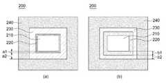
도 4를 참조하면, 노광 마스크(200)는 투광부(210), 투광부(210)를 둘러싸는 제1 차광부(220), 제1 차광부(220)를 둘러싸는 반투광부(230), 반투광부(230)를 둘러싸는 제2 차광부(240)를 포함한다.4, the
투광부(210)는 접촉 구멍 형성용 패턴이고, 원형 또는 다각형 형상일 수 있다. 투광부(210)는 광을 100% 투과시키는 영역이다.The
제1 차광부(220)는 투광부(210)를 둘러싸며, 투광부(210)의 형상에 따라 다르게 형성된다. 제1 차광부(220)는 광을 차단시키는 영역이고, 크롬(Cr)등을 포함할 수 있다. 제1 차광부(220)는 0.1μm 내지 1 μm의 폭(a1,b1)을 가질 수 있다.The first
반투광부(230)는 제1 차광부(220)를 둘러싸며, 투광부(210)의 형상에 따라 다르게 형성된다. 반투광부(230)는 광을 일부만 투과시키는 영역이고, 예를 들면 입사되는 광의 노광량 중 1 내지 10% 범위 내에서 광을 투과 시킬 수 있다. 반투광부(230)는 몰리브덴 실리사이드(MoSi)를 기본으로 질소(N), 산소(O), 탄소(C) 중에서 1 종 이상을 조합하여 MoSiN, MoSiON, MoSiCN, MoSiO, MoSiCON) 등의 위상반전 물질로 이루어진다. 반투광부(230)는 0.1μm 내지 5 μm의 폭(a2,b2)을 가질 수 있다.The
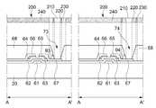
도 5를 참조하면, 본 발명의 노광 마스크(200)를 이용하여 형성된 접촉 구멍(73,74)이 도시되어 있다.Referring to FIG. 5, contact holes 73 and 74 formed using the
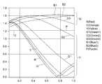
도 6a 내지 도 6e를 참조하면, 제1 차광부(220)의 폭, 반투광부(230)의 폭 및 위상반전물질 투과율에 따른 ILS 값의 변화를 알 수 있다.6A to 6E, the variation of the ILS value according to the width of the first
도 6a 내지 도 6e에 도시된 그래프는 ILS 그래프이다. Y축은 ILS 값이고, X축은 위상반전물질 투과율이다. 각각의 그래프 곡선은 반투광부(230)의 폭에 따라 구분된다. R(Red) 그래프가 반투광부(230)의 폭이 4μm 내지 5μm 인 경우이고, O(Orange) 그래프가 반투광부(230)의 폭이 3μm 내지 4μm 인 경우이고, Y(Yellow) 그래프가 반투광부(230)의 폭이 2.4μm 내지 3μm 인 경우이고, G(Green) 그래프가 반투광부(230)의 폭이 1.0μm 내지 2.4μm 인 경우이고, B(Blue) 그래프가 반투광부(230)의 폭이 0.6μm 내지 1.0μm 인 경우이고, N(Navy) 그래프가 반투광부(230)의 폭이 0.2μm 내지 0.6μm 인 경우이고, P(Purple) 그래프가 반투광부(230)의 폭이 0.01μm 내지 0.2μm 인 경우이다.The graphs shown in Figs. 6A to 6E are ILS graphs. The Y-axis is the ILS value, and the X-axis is the phase reversal material transmittance. Each graph curve is divided according to the width of the
예를 들면, 도 6b의 경우, R은 반투광부(230)의 폭이 4.2 μm인 경우이고, O는 반투광부(230)의 폭이 3.5 μm인 경우이고, Y는 반투광부(230)의 폭이 2.6 μm인 경우이고, G1은 반투광부(230)의 폭이 2.2 μm인 경우이고, G2는 반투광부(230)의 폭이 1.2 μm인 경우이고, G3는 반투광부(230)의 폭이 1.0 μm인 경우이고, B1은 반투광부(230)의 폭이 0.6 μm인 경우이고, B2는 반투광부(230)의 폭이 0.8 μm인 경우이고, P는 반투광부(230)의 폭이 0.01 μm인 경우이다.For example, in the case of FIG. 6B, R represents the case where the width of the
한편, 도 6c의 경우, R은 반투광부(230)의 폭이 4.2 μm인 경우이고, O는 반투광부(230)의 폭이 3.5 μm인 경우이고, Y는 반투광부(230)의 폭이 2.6 μm인 경우이고, G1은 반투광부(230)의 폭이 2.2 μm인 경우이고, G2는 반투광부(230)의 폭이 1.4 μm인 경우이고, G3는 반투광부(230)의 폭이 1.2 μm인 경우이고, G4는 반투광부(230)의 폭이 1.0 μm인 경우이고, B1은 반투광부(230)의 폭이 0.6 μm인 경우이고, B2는 반투광부(230)의 폭이 0.8 μm인 경우이고, P는 반투광부(230)의 폭이 0.01 μm인 경우이다.In the case of FIG. 6C, R represents a case where the width of the
한편, 도 6d의 경우, R은 반투광부(230)의 폭이 4.2 μm인 경우이고, O는 반투광부(230)의 폭이 3.5 μm인 경우이고, Y는 반투광부(230)의 폭이 2.6 μm인 경우이고, G1은 반투광부(230)의 폭이 2.2 μm인 경우이고, G2는 반투광부(230)의 폭이 1.6 μm인 경우이고, G3는 반투광부(230)의 폭이 1.4 μm인 경우이고, G4는 반투광부(230)의 폭이 1.2 μm인 경우이고, G5는 반투광부(230)의 폭이 1.0 μm인 경우이고, B는 반투광부(230)의 폭이 0.6 μm인 경우이고, P는 반투광부(230)의 폭이 0.01 μm인 경우이다.In the case of FIG. 6D, R represents the case where the width of the
한편, 도 6e의 경우, R은 반투광부(230)의 폭이 4.2 μm인 경우이고, O는 반투광부(230)의 폭이 3.5 μm인 경우이고, Y는 반투광부(230)의 폭이 2.6 μm인 경우이고, G1은 반투광부(230)의 폭이 2.2 μm인 경우이고, G2는 반투광부(230)의 폭이 1.8 μm인 경우이고, G3는 반투광부(230)의 폭이 1.4 μm인 경우이고, G4는 반투광부(230)의 폭이 1.2 μm인 경우이고, B는 반투광부(230)의 폭이 0.6 μm인 경우이고, P는 반투광부(230)의 폭이 0.01 μm인 경우이다.6A, R represents a case where the width of the
도 6a는 제1 차광부(220)의 폭이 0μm인 경우이고, 도 6b는 제1 차광부(220)의 폭이 0.2μm인 경우이고, 도 6c는 제1 차광부(220)의 폭이 0.4μm인 경우이고, 도 6d는 제1 차광부(220)의 폭이 0.6μm인 경우이고, 도 6e는 제1 차광부(220)의 폭이 0.8μm인 경우이다. 즉, 도 6a는 기존의 위상반전 마스크를 적용한 ILS 결과값이고, 도 6b 내지 도 6e는 본 발명에 따른 노광 마스크를 적용한 ILS 결과값이다.6A shows a case where the width of the first light-shielding
또한, 10은 ILS가 1.2 수치인 경우로서, 빛의 품질 측면에서의 기준값이다. 즉, ILS 값이 위상반전물질의 투과율에 상관없이 1.2 이상 측정된다면 해상도가 높아졌다고 판단할 수 있다.10 is a reference value in terms of light quality when ILS is 1.2 value. That is, if the ILS value is measured at 1.2 or more regardless of the transmittance of the phase reversal material, it can be judged that the resolution is increased.
도 6a 내지 도 6e에 따른 제1 차광부(220) 및 반투광부(230)의 최적화된 길이비를 검토하면 다음과 같다.The optimized length ratio of the first light-shielding
도 6b의 경우, 제1 차광부(220)와 반투광부(230)는 1:0.9 ~ 1:5의 폭비율을 갖는 것이 바람직하다. 즉, 제1 차광부(220)가 0.2μm의 폭을 가지고 반투광부(230)가 0.2 ~ 1μm 폭을 가질 때, ILS 값이 1.2 이상으로 개선되기 때문이다.In the case of FIG. 6B, it is preferable that the
도 6c의 경우, 제1 차광부(220)와 반투광부(230)는 1:0.5 ~ 1:3.5의 폭비율을 갖는 것이 바람직하다. 즉, 제1 차광부(220)가 0.4μm의 폭을 가지고 반투광부(230)가 0.2 ~ 1.4μm 폭을 가질 때, ILS 값이 1.2 이상으로 개선되기 때문이다.In the case of FIG. 6C, it is preferable that the
도 6d의 경우, 제1 차광부(220)와 반투광부(230)는 1:0.33 ~ 1:2.66의 폭비율을 갖는 것이 바람직하다. 즉, 제1 차광부(220)가 0.6μm의 폭을 가지고 반투광부(230)가 0.2 ~ 1.6μm 폭을 가질 때, ILS 값이 1.2 이상으로 개선되기 때문이다.In the case of FIG. 6D, it is preferable that the first
도 6e의 경우, 제1 차광부(220)와 반투광부(230)는 1:0.25 ~ 1:2.25의 폭비율을 갖는 것이 바람직하다. 즉, 제1 차광부(220)가 0.8μm의 폭을 가지고 반투광부(230)가 0.2 ~ 1.8μm 폭을 가질 때, ILS 값이 1.2 이상으로 개선되기 때문이다.In the case of FIG. 6E, it is preferable that the
즉, 제1 차광부(220)와 반투광부(230)의 폭을 다르게 하여 실험한 도 6b 내지 도 6e의 결과를 종합하면, 제1 차광부(220)와 반투광부(230)는 위상반전물질 투과율에 상관없이 1:0.9 ~ 1:2.25의 폭비율을 갖는 것이 바람직하다.6B to 6E in which the widths of the first
접촉 구멍(73, 74)에 대응되도록 노광 마스크(200)의 각 영역을 배치시킨 뒤, 본 발명에 의하여 개선된 접촉 구멍(73,74)을 도 5 및 도 6a 내지 도 6e를 참조하여 설명하면 다음과 같다.After the respective regions of the
ILS 측면에서 보면, 제1 차광부(220)의 폭을 넓힐수록 위상반전 물질의 투과율에 관계없이 전반적인ILS 값이 상승함을 알 수 있다. 제1 차광부(220)가 없는 기존 위상반전 마스크가 적용된 도 6a의 경우, 11은 반투광부(230)의 폭이 1 내지 5μm이고, 12는 반투광부(230)의 폭이 0.1 내지 0.8μm인 경우이다. 즉, 제1 차광부(220)가 없는 경우, 노광마스크는 반투광부(230)의 폭을 매우 미세하게 적용해야 ILS 값이 상승한다. 그러나 도 6b 내지 도 6e의 경우, 제1 차광부(230)의 폭이 넓어질수록 위상반전물질의 투과율 및 반투광부(230)의 폭에 관계없이 ILS 값이 1.2 이상 값을 갖는 그래프가 늘어난다.From the ILS aspect, it can be seen that as the width of the first
즉, 도 6b 내지 도 6e에서 10에 해당하는 그래프 곡선위로만 그려진 그래프 값을 적절히 선택하여 ILS 값이 개선된 노광 마스크를 제작할 수 있다. 앞서 검토한 바와 같이, 제1 차광부(220)와 반투광부(230)는 1:1 ~ 1:2.25의 폭비율을 갖게 하여 ILS를 개선할 수 있다.That is, an exposure mask having an improved ILS value can be manufactured by appropriately selecting a graph value drawn only on a graph curve corresponding to FIGS. 6B to 6E to 10. As described above, the first
제1 차광부(220)와 반투광부(230)의 폭은 서로 다르게 형성될 수 있다. 제1 차광부(220)의 폭이 더 넓을 수 있고, 반투광부(230)의 폭이 더 넓게 형성될 수 있다. 제1 차광부(220) 및 반투광부(230)의 폭의 차이는 접촉 구멍의 면적에 따라 적절하게 결정될 수 있다.The width of the first light-shielding
위상반전 마스크에 비하여 ILS가 개선되므로 미세한 영역에 보다 많은 노광량의 광이 집중된다. 따라서, 접촉 구멍(73, 74)이 미형성되는 불량률도 낮아지므로 공정 마진도 개선된다.The ILS is improved as compared with the phase inversion mask, so that a larger amount of light is concentrated in the fine region. Therefore, the defect rate at which the contact holes 73 and 74 are not formed is also lowered, so that the process margin is also improved.
절연층(68)의 식각되는 측면에서 보면, 위상반전 마스크에 비하여 절연층(68)이 거의 식각되지 않는다. 즉, 위상반전 마스크는 반투광부가 절연층(68) 상에 존재하므로 절연층(68)에도 광의 노광량 중 일부가 도달한다. 일부 노광된 절연층(68)은 도 3에 도시된 바와 같이 현상 공정시 일부 식각된다. 그러나, 본 발명의 노광 마스크(200)는 접촉 구멍(73,74)이 형성될 영역의 주변에 대응하는 영역에만 반투광부(230)가 형성된다. 나머지 영역은 다시 제2 차광부(240)를 통하여 광을 차단한다. 따라서, 절연층(68)에 광이 도달하지 못하므로 절연층(68)은 식각되지 않는다. 물론, 절연층(68)이 식각됨에 따른 도3에 도시된 절연층(68)의 돌출부(68a)도 생기지 않는다.In view of the etched side of the insulating
앞서 설명한 바와 같이 ILS가 개선되므로, 접촉 구멍(73,74)에서 절연층(68)의 테이퍼 각도가 커진다. 따라서, 보다 미세한 접촉 구멍(73,74)이 형성된다. 예를 들면, 접촉 구멍(73, 74)에서 절연층(68)은 60 도 ~ 90도의 테이퍼각을 갖는다.As described above, since the ILS is improved, the taper angle of the insulating
이와 같이, ILS 및 접촉 구멍의 테이퍼각이 개선되고, 절연층이 식각되지 않음에 따라 전체 공정 마진도 개선된다.Thus, the taper angle of the ILS and the contact hole is improved, and the process margin is also improved as the insulating layer is not etched.
도 5에 도시된 표시장치의 구조를 설명하면 다음과 같다.The structure of the display device shown in FIG. 5 will be described below.
도 5를 참조하면, 유리 또는 플라스틱 등으로 이루어진 기판(20) 상에 게이트 배선(미도시) 및 게이트 전극(61)이 배치된다. 게이트 배선은 게이트 배선으로부터 돌출한 복수의 게이트 전극(gate electrode)(61)과 다른 층 또는 외부 구동 회로와의 접속을 위하여 면적이 넓은 끝 부분에 해당하는 게이트 패드(미도시)을 포함한다.Referring to FIG. 5, a gate wiring (not shown) and a
게이트 배선(미도시) 및 게이트 전극(61) 위에는 질화규소(SiNx) 또는 산화규소(SiOx) 따위로 만들어진 게이트 절연막(gate insulating layer)(62)이 형성되어 있다.A
게이트 절연막(62) 위에는 수소화 비정질 규소(hydrogenated amorphous silicon)(비정질 규소는 약칭 a-Si로 씀) 또는 다결정 규소(polysilicon) 등으로 만들어진 복수의 반도체(63)가 형성되어 있다. 반도체(63)는 주로 세로 방향으로 뻗으며, 게이트 전극(61)을 향하여 뻗어 나온 복수의 돌출부(projection)(미도시)를 포함한다.On the
상기 복수의 반도체(63)는 산화물 반도체이다. 상기 산화물 반도체는 아연(Zn), 갈륨(Ga), 인듐(In) 및 주석(Sn)으로 이루어진 군에서 선택된 적어도 하나를 포함할 수 있다.The plurality of
예컨대, 상기 산화물 반도체는 아연(Zn), 갈륨(Ga), 주석(Sn) 또는 인듐(In)을 기본으로 하는 산화물, 또는 복합 산화물인 산화아연(ZnO), 인듐-갈륨-아연 산화물(InGaZnO4), 인듐-아연 산화물(In-Zn-O), 아연-주석 산화물(Zn-Sn-O) 등과 같은 산화물 반도체 재료를 이용하여 만들어질 수 있다.For example, the oxide semiconductor may be an oxide based on zinc (Zn), gallium (Ga), tin (Sn), or indium (In), or a complex oxide such as zinc oxide (ZnO), indium-gallium-zinc oxide (InGaZnO4) , Indium-zinc oxide (In-Zn-O), zinc-tin oxide (Zn-Sn-O), and the like.
구체적으로, 상기 산화물 반도체는 인듐(In), 갈륨(Ga), 아연(Zn) 및 산소(O)를 포함하는 IGZO계의 산화물을 포함할 수 있다. 이외에도 상기 산화물 반도체는 In-Sn-Zn-O계 금속 산화물, In-Al-Zn-O계 금속 산화물, Sn-Ga-Zn-O계 금속 산화물, Al-Ga-Zn-O계 금속 산화물, Sn-Al-Zn-O계 금속 산화물, In-Zn-O계 금속 산화물, Sn-Zn-O계 금속 산화물, Al-Zn-O계 금속 산화물, In-O계 금속 산화물, Sn-O계 금속 산화물, 및 Zn-O계 금속 산화물을 포함할 수 있다.Specifically, the oxide semiconductor may include an oxide of an IGZO system including indium (In), gallium (Ga), zinc (Zn), and oxygen (O). The oxide semiconductor may be an In-Sn-Zn-O based metal oxide, an In-Al-Zn-O based metal oxide, a Sn-Ga-Zn-O based metal oxide, an Al- Zn-O-based metal oxide, In-O-based metal oxide, Sn-O-based metal oxide, Sn-Zn-O-based metal oxide, , And a Zn-O-based metal oxide.
반도체(63) 위에는 복수의 저항성 접촉 부재(ohmic contact)(64, 65)가 형성되어 있고, 접촉 저항을 낮추어 주는 역할을 한다. 저항성 접촉 부재(64, 65)는 인(P) 따위의 n형 불순물이 고농도로 도핑되어 있는 n+ 수소화 비정질 규소 따위의 물질로 만들어지거나 실리사이드(silicide)로 만들어질 수 있다.On the
저항성 접촉 부재(64, 65) 및 게이트 절연막(62) 위에는 복수의 데이터 배선(data line)(미도시)과 복수의 드레인 전극(drain electrode)(67)이 형성되어 있다.A plurality of data lines (not shown) and a plurality of
각 데이터 배선(미도시)은 게이트 전극(61)을 향하여 뻗은 복수의 소스 전극(source electrode)(66)과 다른 층 또는 외부 구동회로와의 접속을 위하여 면적이 넓은 끝 부분에 해당하는 데이터 패드(미도시)를 포함한다.Each data line (not shown) includes a plurality of
드레인 전극(67)은 데이터 배선(미도시)과 분리되어 있고 게이트 전극(61)을 중심으로 소스 전극(66)과 마주 본다.The
구체적으로, 소스 전극(66), 드레인 전극(67) 및 데이터 배선(미도시)은 몰리브덴, 크롬, 탄탈륨 및 티타늄 등 내화성 금속(refractory metal) 또는 이들의 합금에 의하여 형성될 수 있으며, 상기 내화성 금속막과 저저항 도전막을 포함하는 다중막 구조를 가질 수도 있다. 상기 다중막 구조의 예로, 크롬 또는 몰리브덴(합금) 하부막과 알루미늄(합금) 상부막으로 된 이중막, 몰리브덴(합금) 하부막과 알루미늄(합금) 중간막과 몰리브덴(합금) 상부막으로 된 삼중막을 들 수 있다.Specifically, the
하나의 게이트 전극(61), 하나의 소스 전극(66) 및 하나의 드레인 전극(67)은 반도체(63)의 돌출부(미도시)와 함께 하나의 박막 트랜지스터(thin film transistor, TFT)를 이루며, 박막 트랜지스터의 채널(channel)은 소스 전극(66)과 드레인 전극(67) 사이의 돌출부에 형성된다.One
게이트 배선(미도시), 데이터 배선(미도시), 소스 전극(66), 드레인 전극(67) 및 노출된 반도체(63) 부분 위에는 보호막(68)이 형성된다. 보호막(passivation layer)(68)은 플라즈마 도움 화학기상 증착법 (Plasma Enhanced Chemical Vapor Deposition, PRCVD) 등의 증착방법으로 SiNx, SiOx와 같은 무기 절연물질, 유전상수가 작은 아크릴(acryl)계 유기화합물, BCB(Benzocyclobytane) 또는 PFCB(Perfluorocyclobytane) 등과 같은 유기 절연물질, 또는 상기 무기 절연물질과 유기 절연물질의 적층구조로 평탄화되어 형성된다.A
보호막(68)은 드레인 전극(67)을 각각 드러내는 복수의 드레인 접촉 구멍(contact hole)(73,74), 게이트 패드(미도시)를 각각 드러내는 복수의 게이트 패드 접촉 구멍(미도시) 및 데이터 패드(미도시)를 각각 드러내는 복수의 데이터 패드 접촉 구멍(미도시)을 구비한다.The
보호막(68) 위에는 복수의 화소 전극(pixel electrode)(미도시)이 형성되어 있다. 화소 전극은 ITO 또는 IZO 등의 투명한 도전 물질이나 알루미늄, 은 또는 그 합금 등의 반사성 금속으로 만들어질 수 있다.A plurality of pixel electrodes (not shown) are formed on the
화소 전극(미도시)은 접촉 구멍(73,74)을 통하여 드레인 전극(67)과 물리적?전기적으로 연결되어 있으며, 드레인 전극(67)으로부터 데이터 전압을 인가 받는다. 데이터 전압이 인가된 화소 전극(191)은 공통 전압(common voltage)을 인가 받는 다른 표시판(도시하지 않음)의 공통 전극(common electrode)(도시하지 않음)과 함께 전기장을 생성함으로써 두 전극 사이의 액정층(도시하지 않음)의 액정 분자의 방향을 결정한다. 화소 전극과 공통 전극은 축전기[이하 “액정 축전기(liquid crystal capacitor)”라 함]를 이루어 박막 트랜지스터가 턴 오프(turn-off)된 후에도 인가된 전압을 유지한다.A pixel electrode (not shown) is physically and electrically connected to the
한편, 본 발명이 유기 발광 표시 장치로 구성될 경우, 본 발명은 화소 전극(미도시) 상에 형성된 유기 발광층(미도시) 및 상기 유기 발광층 상에 형성된 대향 전극(미도시)을 포함한다.When the present invention is configured as an organic light emitting display, the present invention includes an organic light emitting layer (not shown) formed on a pixel electrode (not shown) and an opposite electrode (not shown) formed on the organic light emitting layer.
화소 전극(미도시)은 화소 정의막(미도시)의 개구부에 대응하도록 배치되는데, 화소 전극이 반드시 화소 정의막의 개구부에만 배치되는 것은 아니며, 화소 전극의 일부가 화소 정의막과 중첩되도록 화소 정의막 아래에 배치될 수 있다. 화소정의막은 폴리아크릴계 수지(polyacrylates resin) 및 폴리이미드계(polyimides) 등의 수지 또는 실리카 계열의 무기물 등으로 만들 수 있다.The pixel electrode (not shown) is arranged to correspond to the opening of the pixel defining layer (not shown). The pixel electrode is not necessarily arranged only in the opening of the pixel defining layer, Can be placed underneath. The pixel defining layer may be made of a resin such as polyacrylates resin or polyimide, or a silica-based inorganic material.
화소 전극 위에는 유기 발광층(미도시)이 형성되고, 유기 발광층 상에는 캐소드 전극이 되는 대향 전극(미도시)이 형성된다. 이와 같이, 화소 전극, 유기 발광층 및 대향 전극을 포함하는 유기 발광 표시 장치가 형성된다.An organic light emitting layer (not shown) is formed on the pixel electrode, and a counter electrode (not shown) is formed on the organic light emitting layer to serve as a cathode electrode. Thus, an organic light emitting display including a pixel electrode, an organic light emitting layer, and a counter electrode is formed.
이상에서 설명된 표시장치 및 그 제조방법의 실시예는 예시적인 것에 불과하며, 본 발명의 보호범위는 본 발명 기술분야의 통상의 지식을 가진 자라면 이로부터 다양한 변형 및 균등예를 포함할 수 있다.The embodiments of the display device and the manufacturing method thereof described above are merely illustrative, and the scope of protection of the present invention may include various modifications and equivalents to those skilled in the art .
1,4:석영기판2:광차단막
3,6:개구부5:위상반전막
20:기판30:바이너리 마스크
31:투광부32:차광부
40:위상반전마스크41:투광부
42:반투광부61:게이트전극
62:게이트절연막63:반도체
64,65:저항성 접촉 부재66:소스 전극
67:드레인 전극68:보호막
68a:보호막 돌출부71,72,73,74:접촉 구멍
80:실링부재200:노광 마스크
210:투광영역220:제1 차광부
230:반투광부240:제2 차광부1,4: quartz substrate 2: light blocking film
3, 6: opening 5: phase reversing film
20: substrate 30: binary mask
31: transparent portion 32:
40: phase inversion mask 41:
42: translucent portion 61: gate electrode
62: gate insulating film 63: semiconductor
64, 65: resistive contact member 66: source electrode
67: drain electrode 68: protective film
68a:
80: sealing member 200: exposure mask
210: a light transmitting region 220: a first light-
230: translucent portion 240: second miner
Claims (19)
Translated fromKorean상기 기판 상에 배치된 게이트 배선 및 데이터 배선;
상기 기판 상에 형성되며, 상기 게이트 배선 및 데이터 배선과 연결된 박막 트랜지스터;
상기 박막 트랜지스터와 연결된 화소전극; 및
상기 기판 상에 배치된 절연층을 포함하고,
상기 절연층은 접촉 구멍을 구비하고, 상기 접촉 구멍에서 절연층은 60도 내지 90도의 테이퍼각을 갖는 표시장치.Board;
A gate wiring and a data wiring disposed on the substrate;
A thin film transistor formed on the substrate and connected to the gate wiring and the data wiring;
A pixel electrode connected to the thin film transistor; And
And an insulating layer disposed on the substrate,
Wherein the insulating layer has a contact hole, and the insulating layer in the contact hole has a taper angle of 60 to 90 degrees.
상기 절연층은 반도체층, 드레인 전극, 게이트 배선, 데이터 배선 및 패드 전극 중 적어도 하나를 덮는 표시장치.The method according to claim 1,
Wherein the insulating layer covers at least one of a semiconductor layer, a drain electrode, a gate wiring, a data wiring, and a pad electrode.
상기 접촉 구멍은 반도체층, 드레인 전극, 게이트 배선, 데이터 배선 및 패드 전극 중 어느 하나를 노출시키는 표시장치.The method according to claim 1,
Wherein the contact hole exposes any one of a semiconductor layer, a drain electrode, a gate wiring, a data wiring and a pad electrode.
상기 투광부를 둘러싸는 제1 차광부;
상기 제1 차광부를 둘러싸는 반투광부; 및
상기 반투광부를 둘러싸는 제2 차광부;를 포함하는 노광 마스크.A transparent portion;
A first light-shielding portion surrounding the light-transmitting portion;
A semi-transmissive portion surrounding the first light-shielding portion; And
And a second light-shielding portion surrounding the semi-light-transmitting portion.
상기 제1 차광부와 상기 반투광부는 서로 다른 폭을 갖는 노광 마스크.5. The method of claim 4,
Wherein the first light-shielding portion and the semi-light-transmitting portion have different widths.
상기 투광부는 원형 또는 다각형 형상인 노광 마스크.5. The method of claim 4,
Wherein the light transmitting portion has a circular or polygonal shape.
상기 투광부는 접촉 구멍 형성용 패턴인 노광마스크.5. The method of claim 4,
Wherein the light transmitting portion is a contact hole forming pattern.
상기 제1 차광부와 상기 반투광부는 1:0.9 내지 1:2.25의 폭비율을 갖는 노광마스크.5. The method of claim 4,
Wherein the first light-shielding portion and the semi-light-transmitting portion have a width ratio of 1: 0.9 to 1: 2.25.
상기 제1 차광부는 0.1μm 내지 1 μm의 폭을 갖는 노광마스크.9. The method of claim 8,
Wherein the first light-shielding portion has a width of 0.1 mu m to 1 mu m.
상기 반투광부는 0.1μm 내지 5 μm의 폭을 갖는 노광마스크.9. The method of claim 8,
Wherein the translucent portion has a width of 0.1 占 퐉 to 5 占 퐉.
노광 마스크를 이용하여 상기 절연층을 노광시키는 단계; 및
노광된 상기 절연층을 현상하여 접촉 구멍을 형성하는 단계;를 포함하고,
상기 노광 마스크는,
투광부;
상기 투광부를 둘러싸는 제1 차광부;
상기 제1 차광부를 둘러싸는 반투광부; 및
상기 반투광부를 둘러싸는 제2 차광부;를 포함하는 표시장치의 제조방법.Forming an insulating layer on the substrate;
Exposing the insulating layer using an exposure mask; And
And developing the exposed insulating layer to form a contact hole,
In the exposure mask,
A transparent portion;
A first light-shielding portion surrounding the light-transmitting portion;
A semi-transmissive portion surrounding the first light-shielding portion; And
And a second light-shielding portion surrounding the translucent portion.
상기 제1 차광부와 상기 반투광부는 서로 다른 폭을 갖는 표시장치의 제조방법.12. The method of claim 11,
Wherein the first light-shielding portion and the translucent portion have different widths.
상기 투광부, 상기 제1 차광부 및 상기 반투광부는 상기 접촉 구멍이 형성되는 영역 상에 배치되는 표시장치의 제조방법.12. The method of claim 11,
Wherein the transparent portion, the first light-shielding portion, and the translucent portion are disposed on a region where the contact hole is formed.
상기 접촉 구멍에서 상기 절연층은 60도 내지 90도의 테이퍼각을 갖는 표시장치의 제조방법.12. The method of claim 11,
And the insulating layer in the contact hole has a taper angle of 60 to 90 degrees.
상기 투광부는 원형 또는 다각형 형상인 표시장치의 제조방법.12. The method of claim 11,
Wherein the light transmitting portion has a circular or polygonal shape.
상기 투광부는 접촉 구멍 형성용 패턴인 표시장치의 제조방법.12. The method of claim 11,
Wherein the light transmitting portion is a contact hole forming pattern.
상기 제1 차광부와 상기 반투광부는 1:0.9 내지 1:2.25의 폭비율을 갖는 표시장치의 제조방법.12. The method of claim 11,
Wherein the first light-shielding portion and the translucent portion have a width ratio of 1: 0.9 to 1: 2.25.
상기 제1 차광부는 0.1μm 내지 1 μm의 폭을 갖는 표시장치의 제조방법.18. The method of claim 17,
Wherein the first light-shielding portion has a width of 0.1 占 퐉 to 1 占 퐉.
상기 반투광부는 0.1μm 내지 5 μm의 폭을 갖는 표시장치의 제조방법.18. The method of claim 17,
Wherein the translucent portion has a width of 0.1 占 퐉 to 5 占 퐉.
Priority Applications (2)
| Application Number | Priority Date | Filing Date | Title |
|---|---|---|---|
| KR1020140015334AKR102248240B1 (en) | 2014-02-11 | 2014-02-11 | Display device and method of manufacturing display device using the same |
| US14/509,774US20150228665A1 (en) | 2014-02-11 | 2014-10-08 | Display device and method of manufacturing the same |
Applications Claiming Priority (1)
| Application Number | Priority Date | Filing Date | Title |
|---|---|---|---|
| KR1020140015334AKR102248240B1 (en) | 2014-02-11 | 2014-02-11 | Display device and method of manufacturing display device using the same |
Publications (2)
| Publication Number | Publication Date |
|---|---|
| KR20150094856Atrue KR20150094856A (en) | 2015-08-20 |
| KR102248240B1 KR102248240B1 (en) | 2021-05-06 |
Family
ID=53775630
Family Applications (1)
| Application Number | Title | Priority Date | Filing Date |
|---|---|---|---|
| KR1020140015334AActiveKR102248240B1 (en) | 2014-02-11 | 2014-02-11 | Display device and method of manufacturing display device using the same |
Country Status (2)
| Country | Link |
|---|---|
| US (1) | US20150228665A1 (en) |
| KR (1) | KR102248240B1 (en) |
Cited By (1)
| Publication number | Priority date | Publication date | Assignee | Title |
|---|---|---|---|---|
| KR20180007376A (en)* | 2016-07-12 | 2018-01-23 | 삼성디스플레이 주식회사 | Display Apparatus and Method for manufacturing the same |
Families Citing this family (3)
| Publication number | Priority date | Publication date | Assignee | Title |
|---|---|---|---|---|
| TWI553388B (en)* | 2014-09-11 | 2016-10-11 | 群創光電股份有限公司 | Liquid crystal display device and component substrate thereof |
| CN110634410A (en)* | 2019-10-21 | 2019-12-31 | 昆山国显光电有限公司 | Display device |
| JP7731678B2 (en)* | 2020-03-16 | 2025-09-01 | Hoya株式会社 | Photomask and display device manufacturing method |
Citations (3)
| Publication number | Priority date | Publication date | Assignee | Title |
|---|---|---|---|---|
| JP2001296647A (en)* | 2000-02-10 | 2001-10-26 | Nec Corp | Photomask and exposure method using the same |
| KR20100027444A (en)* | 2008-09-02 | 2010-03-11 | 주식회사 동부하이텍 | Mask pattern, and method of fabricating semiconductor device using the same |
| US20120105778A1 (en)* | 2010-10-29 | 2012-05-03 | Panasonic Liquid Crystal Display Co., Ltd. | Liquid crystal display device |
Family Cites Families (3)
| Publication number | Priority date | Publication date | Assignee | Title |
|---|---|---|---|---|
| KR100929675B1 (en)* | 2003-03-24 | 2009-12-03 | 삼성전자주식회사 | Multi-domain liquid crystal display device and thin film transistor substrate thereof |
| JP5771377B2 (en)* | 2010-10-05 | 2015-08-26 | 株式会社ジャパンディスプレイ | Manufacturing method of display device |
| JP2012248743A (en)* | 2011-05-30 | 2012-12-13 | Japan Display West Co Ltd | Semiconductor device, manufacturing method of the semiconductor device, display device, and electronic apparatus |
- 2014
- 2014-02-11KRKR1020140015334Apatent/KR102248240B1/enactiveActive
- 2014-10-08USUS14/509,774patent/US20150228665A1/ennot_activeAbandoned
Patent Citations (3)
| Publication number | Priority date | Publication date | Assignee | Title |
|---|---|---|---|---|
| JP2001296647A (en)* | 2000-02-10 | 2001-10-26 | Nec Corp | Photomask and exposure method using the same |
| KR20100027444A (en)* | 2008-09-02 | 2010-03-11 | 주식회사 동부하이텍 | Mask pattern, and method of fabricating semiconductor device using the same |
| US20120105778A1 (en)* | 2010-10-29 | 2012-05-03 | Panasonic Liquid Crystal Display Co., Ltd. | Liquid crystal display device |
Cited By (2)
| Publication number | Priority date | Publication date | Assignee | Title |
|---|---|---|---|---|
| KR20180007376A (en)* | 2016-07-12 | 2018-01-23 | 삼성디스플레이 주식회사 | Display Apparatus and Method for manufacturing the same |
| US12040425B2 (en) | 2016-07-12 | 2024-07-16 | Samsung Display Co., Ltd. | Self-aligned display appartus |
Also Published As
| Publication number | Publication date |
|---|---|
| US20150228665A1 (en) | 2015-08-13 |
| KR102248240B1 (en) | 2021-05-06 |
Similar Documents
| Publication | Publication Date | Title |
|---|---|---|
| US10288965B2 (en) | Method for producing semiconductor device for high definition | |
| CN106802519B (en) | Liquid crystal display device and method of manufacturing the same | |
| JP4908330B2 (en) | Method for manufacturing array substrate for liquid crystal display device | |
| JP5336102B2 (en) | TFT substrate | |
| KR100380142B1 (en) | Transflective liquid crystal display device | |
| US10191331B2 (en) | Mask and method of fabricating display device using the mask | |
| US20130222726A1 (en) | Liquid crystal display device and method of fabricating the same | |
| KR20120014749A (en) | Display substrate, display device and manufacturing method thereof | |
| KR102304991B1 (en) | Thin film transistor array substrate and method of manufacturing thereof and display device having the thin film transistor array substrate | |
| US9786694B2 (en) | Display device and manufacturing method thereof | |
| KR102248240B1 (en) | Display device and method of manufacturing display device using the same | |
| KR20130129673A (en) | Thin film transistor array panel and method for manufacturing the same | |
| US20150255493A1 (en) | Display device and method of manufacturing the same | |
| JP5090133B2 (en) | Liquid crystal display | |
| KR102461634B1 (en) | Liquid crystal display device and manufacturing method thereof | |
| KR102153002B1 (en) | Fringe field switching liquid crystal display device and method of fabricating the same | |
| KR20160066580A (en) | Display device | |
| KR20040026978A (en) | Array Panel used for a Liquid Crystal Display Device having a Repair Structure | |
| KR20090029572A (en) | Array substrate for liquid crystal display device and manufacturing method thereof | |
| KR20200105458A (en) | Display device and method of manufacturing display device using the same | |
| KR20050102442A (en) | Thin film transistor array panel and method for manufacturing the same | |
| KR20060019028A (en) | Thin film transistor array panel and manufacturing method thereof | |
| KR20050011874A (en) | Thin film transistor array panel | |
| KR20060046222A (en) | Method of manufacturing thin film transistor array panel | |
| KR20060082313A (en) | Liquid crystal display |
Legal Events
| Date | Code | Title | Description |
|---|---|---|---|
| PA0109 | Patent application | Patent event code:PA01091R01D Comment text:Patent Application Patent event date:20140211 | |
| PG1501 | Laying open of application | ||
| A201 | Request for examination | ||
| PA0201 | Request for examination | Patent event code:PA02012R01D Patent event date:20190211 Comment text:Request for Examination of Application Patent event code:PA02011R01I Patent event date:20140211 Comment text:Patent Application | |
| E902 | Notification of reason for refusal | ||
| PE0902 | Notice of grounds for rejection | Comment text:Notification of reason for refusal Patent event date:20200629 Patent event code:PE09021S01D | |
| E701 | Decision to grant or registration of patent right | ||
| PE0701 | Decision of registration | Patent event code:PE07011S01D Comment text:Decision to Grant Registration Patent event date:20210128 | |
| GRNT | Written decision to grant | ||
| PR0701 | Registration of establishment | Comment text:Registration of Establishment Patent event date:20210428 Patent event code:PR07011E01D | |
| PR1002 | Payment of registration fee | Payment date:20210429 End annual number:3 Start annual number:1 | |
| PG1601 | Publication of registration | ||
| PR1001 | Payment of annual fee | Payment date:20240321 Start annual number:4 End annual number:4 |