KR20150090634A - Display driving intergrated circuit, display driving device and operation method of display driving intergrated circuit - Google Patents
Display driving intergrated circuit, display driving device and operation method of display driving intergrated circuitDownload PDFInfo
- Publication number
- KR20150090634A KR20150090634AKR1020140011524AKR20140011524AKR20150090634AKR 20150090634 AKR20150090634 AKR 20150090634AKR 1020140011524 AKR1020140011524 AKR 1020140011524AKR 20140011524 AKR20140011524 AKR 20140011524AKR 20150090634 AKR20150090634 AKR 20150090634A
- Authority
- KR
- South Korea
- Prior art keywords
- data
- input
- random number
- output
- input data
- Prior art date
- Legal status (The legal status is an assumption and is not a legal conclusion. Google has not performed a legal analysis and makes no representation as to the accuracy of the status listed.)
- Withdrawn
Links
Images


Classifications
- G—PHYSICS
- G09—EDUCATION; CRYPTOGRAPHY; DISPLAY; ADVERTISING; SEALS
- G09G—ARRANGEMENTS OR CIRCUITS FOR CONTROL OF INDICATING DEVICES USING STATIC MEANS TO PRESENT VARIABLE INFORMATION
- G09G3/00—Control arrangements or circuits, of interest only in connection with visual indicators other than cathode-ray tubes
- G09G3/20—Control arrangements or circuits, of interest only in connection with visual indicators other than cathode-ray tubes for presentation of an assembly of a number of characters, e.g. a page, by composing the assembly by combination of individual elements arranged in a matrix no fixed position being assigned to or needed to be assigned to the individual characters or partial characters
- G09G3/34—Control arrangements or circuits, of interest only in connection with visual indicators other than cathode-ray tubes for presentation of an assembly of a number of characters, e.g. a page, by composing the assembly by combination of individual elements arranged in a matrix no fixed position being assigned to or needed to be assigned to the individual characters or partial characters by control of light from an independent source
- G09G3/36—Control arrangements or circuits, of interest only in connection with visual indicators other than cathode-ray tubes for presentation of an assembly of a number of characters, e.g. a page, by composing the assembly by combination of individual elements arranged in a matrix no fixed position being assigned to or needed to be assigned to the individual characters or partial characters by control of light from an independent source using liquid crystals
- G09G3/3607—Control arrangements or circuits, of interest only in connection with visual indicators other than cathode-ray tubes for presentation of an assembly of a number of characters, e.g. a page, by composing the assembly by combination of individual elements arranged in a matrix no fixed position being assigned to or needed to be assigned to the individual characters or partial characters by control of light from an independent source using liquid crystals for displaying colours or for displaying grey scales with a specific pixel layout, e.g. using sub-pixels
- G—PHYSICS
- G09—EDUCATION; CRYPTOGRAPHY; DISPLAY; ADVERTISING; SEALS
- G09G—ARRANGEMENTS OR CIRCUITS FOR CONTROL OF INDICATING DEVICES USING STATIC MEANS TO PRESENT VARIABLE INFORMATION
- G09G3/00—Control arrangements or circuits, of interest only in connection with visual indicators other than cathode-ray tubes
- G09G3/20—Control arrangements or circuits, of interest only in connection with visual indicators other than cathode-ray tubes for presentation of an assembly of a number of characters, e.g. a page, by composing the assembly by combination of individual elements arranged in a matrix no fixed position being assigned to or needed to be assigned to the individual characters or partial characters
- G09G3/2085—Special arrangements for addressing the individual elements of the matrix, other than by driving respective rows and columns in combination
- G—PHYSICS
- G09—EDUCATION; CRYPTOGRAPHY; DISPLAY; ADVERTISING; SEALS
- G09G—ARRANGEMENTS OR CIRCUITS FOR CONTROL OF INDICATING DEVICES USING STATIC MEANS TO PRESENT VARIABLE INFORMATION
- G09G3/00—Control arrangements or circuits, of interest only in connection with visual indicators other than cathode-ray tubes
- G09G3/20—Control arrangements or circuits, of interest only in connection with visual indicators other than cathode-ray tubes for presentation of an assembly of a number of characters, e.g. a page, by composing the assembly by combination of individual elements arranged in a matrix no fixed position being assigned to or needed to be assigned to the individual characters or partial characters
- G09G3/2092—Details of a display terminals using a flat panel, the details relating to the control arrangement of the display terminal and to the interfaces thereto
- G09G3/2096—Details of the interface to the display terminal specific for a flat panel
- G—PHYSICS
- G09—EDUCATION; CRYPTOGRAPHY; DISPLAY; ADVERTISING; SEALS
- G09G—ARRANGEMENTS OR CIRCUITS FOR CONTROL OF INDICATING DEVICES USING STATIC MEANS TO PRESENT VARIABLE INFORMATION
- G09G3/00—Control arrangements or circuits, of interest only in connection with visual indicators other than cathode-ray tubes
- G09G3/20—Control arrangements or circuits, of interest only in connection with visual indicators other than cathode-ray tubes for presentation of an assembly of a number of characters, e.g. a page, by composing the assembly by combination of individual elements arranged in a matrix no fixed position being assigned to or needed to be assigned to the individual characters or partial characters
- G09G3/34—Control arrangements or circuits, of interest only in connection with visual indicators other than cathode-ray tubes for presentation of an assembly of a number of characters, e.g. a page, by composing the assembly by combination of individual elements arranged in a matrix no fixed position being assigned to or needed to be assigned to the individual characters or partial characters by control of light from an independent source
- G09G3/36—Control arrangements or circuits, of interest only in connection with visual indicators other than cathode-ray tubes for presentation of an assembly of a number of characters, e.g. a page, by composing the assembly by combination of individual elements arranged in a matrix no fixed position being assigned to or needed to be assigned to the individual characters or partial characters by control of light from an independent source using liquid crystals
- G09G3/3611—Control of matrices with row and column drivers
- G09G3/3685—Details of drivers for data electrodes
- G09G3/3688—Details of drivers for data electrodes suitable for active matrices only
- G—PHYSICS
- G09—EDUCATION; CRYPTOGRAPHY; DISPLAY; ADVERTISING; SEALS
- G09G—ARRANGEMENTS OR CIRCUITS FOR CONTROL OF INDICATING DEVICES USING STATIC MEANS TO PRESENT VARIABLE INFORMATION
- G09G2310/00—Command of the display device
- G09G2310/02—Addressing, scanning or driving the display screen or processing steps related thereto
- G09G2310/0264—Details of driving circuits
- G09G2310/0286—Details of a shift registers arranged for use in a driving circuit
- G—PHYSICS
- G09—EDUCATION; CRYPTOGRAPHY; DISPLAY; ADVERTISING; SEALS
- G09G—ARRANGEMENTS OR CIRCUITS FOR CONTROL OF INDICATING DEVICES USING STATIC MEANS TO PRESENT VARIABLE INFORMATION
- G09G2310/00—Command of the display device
- G09G2310/08—Details of timing specific for flat panels, other than clock recovery
- G—PHYSICS
- G09—EDUCATION; CRYPTOGRAPHY; DISPLAY; ADVERTISING; SEALS
- G09G—ARRANGEMENTS OR CIRCUITS FOR CONTROL OF INDICATING DEVICES USING STATIC MEANS TO PRESENT VARIABLE INFORMATION
- G09G2330/00—Aspects of power supply; Aspects of display protection and defect management
- G09G2330/02—Details of power systems and of start or stop of display operation
- G09G2330/021—Power management, e.g. power saving
- G—PHYSICS
- G09—EDUCATION; CRYPTOGRAPHY; DISPLAY; ADVERTISING; SEALS
- G09G—ARRANGEMENTS OR CIRCUITS FOR CONTROL OF INDICATING DEVICES USING STATIC MEANS TO PRESENT VARIABLE INFORMATION
- G09G2330/00—Aspects of power supply; Aspects of display protection and defect management
- G09G2330/06—Handling electromagnetic interferences [EMI], covering emitted as well as received electromagnetic radiation
Landscapes
- Engineering & Computer Science (AREA)
- Physics & Mathematics (AREA)
- Computer Hardware Design (AREA)
- General Physics & Mathematics (AREA)
- Theoretical Computer Science (AREA)
- Chemical & Material Sciences (AREA)
- Crystallography & Structural Chemistry (AREA)
- Control Of Indicators Other Than Cathode Ray Tubes (AREA)
- Multimedia (AREA)
Abstract
Translated fromKorean
Description
Translated fromKorean본 발명의 기술적 사상은, 디스플레이 구동 집적회로, 디스플레이 장치 및 디스플레이 구동 집적회로의 동작 방법에 관한 것으로, 자세하게는 전력 소모를 줄이면서도 EMI(Electro Magnetic Interference) 잡음을 감쇄시킬 수 있는 디스플레이 구동 집적회로, 디스플레이 장치 및 디스플레이 구동 집적회로의 동작 방법에 관한 것이다.Technical Field The present invention relates to a display driving integrated circuit, a display device, and a display driving integrated circuit, and more particularly, to a display driving integrated circuit capable of reducing EMI (Electro Magnetic Interference) noise while reducing power consumption, A display device, and a method of operating a display driving integrated circuit.
디스플레이 장치에 대한 고해상도의 요구에 따라 디스플레이를 구동하는데 사용되는 주파수가 높아지고 있다. 이에 따라, 디스플레이 구동 집적회로 또는 디스플레이 장치에서의 전력 소모 및 EMI 잡음 문제가 야기되고 있다.The frequency used for driving the display is increasing according to the demand for high resolution of the display device. As a result, power consumption and EMI noise in a display driving integrated circuit or a display device are caused.
본 발명의 기술적 사상은 전력 소모를 줄이면서도 EMI(Electro Magnetic Interference) 잡음을 감쇄시킬 수 있는 디스플레이 구동 집적회로, 디스플레이 장치 및 디스플레이 구동 집적회로의 동작 방법을 제공한다.The technical idea of the present invention provides a display driving integrated circuit, a display device, and an operation method of a display driving integrated circuit capable of attenuating Electro Magnetic Interference (EMI) noise while reducing power consumption.
본 발명의 일 실시예에 따른 디스플레이 구동 집적회로는, 입력되는 입력 데이터를 처리하여 출력 데이터로 출력하는 타이밍 컨트롤러(time controller); 및 상기 타이밍 컨트롤러와 연결되는 전송 채널을 통해 입력되는 상기 출력 데이터를 아날로그 변환하여 디스플레이 데이터로 출력하는 적어도 하나 이상의 소스 드라이버(source driver)를 구비하는 소스 구동부를 포함하고, 상기 타이밍 컨트롤러는, 상기 입력 데이터의 천이 개수, 및 상기 입력 데이터를 인코딩한 인코디드 데이터의 천이 개수를 비교한 비교 결과에 따라, 상기 입력 데이터 및 상기 인코디드 데이터 중 하나를 선택 데이터로 출력하는 데이터 선택부; 상기 선택 데이터를 난수화하여 난수 데이터로 생성하는 데이터 난수화부; 및 상기 난수 데이터를 상기 출력 데이터로 변환하는 데이터 전송부를 포함한다.A display driver IC according to an exemplary embodiment of the present invention includes a timing controller for processing inputted input data and outputting the input data as output data; And a source driver having at least one source driver for analog-converting the output data input through a transmission channel connected to the timing controller and outputting the converted output data as display data, A data selector for outputting one of the input data and the incoded data as selection data according to a comparison result obtained by comparing the number of transitions of the data and the number of transitions of the encoded data that has encoded the input data; A data randomizer for randomizing the selection data to generate random number data; And a data transfer unit for converting the random number data into the output data.
상기 데이터 선택부는, 상기 입력 데이터가 입력되는 데이터 입력부; 상기 입력 데이터의 천이 개수를 제1 값으로 산출하는 제1 천이 산출부; 상기 입력 데이터를 상기 인코디드 데이터로 인코딩하는 데이터 인코딩부; 상기 인코디드 데이터의 천이 개수를 제2 값으로 산출하는 제2 천이 산출부; 상기 제1 값 및 상기 제2 값을 비교하여 상기 비교 결과로 출력하는 비교부; 및 상기 비교 결과에 따라, 상기 입력 데이터 및 상기 인코디드 데이터 중 하나를 출력하는 데이터 출력부를 포함할 수 있다.Wherein the data selection unit comprises: a data input unit to which the input data is input; A first transition calculation unit for calculating a transition number of the input data as a first value; A data encoding unit encoding the input data into the encoded data; A second transition calculation unit for calculating a transition number of the encoded data as a second value; A comparison unit comparing the first value and the second value and outputting the comparison result; And a data output unit outputting one of the input data and the incoded data according to the comparison result.
상기 데이터 인코딩부는, 상기 입력 데이터의 연속된 첫 번째 픽셀 데이터 내지 M 번째 픽셀 데이터를, 상기 첫 번째 픽셀 데이터 및 상기 입력 데이터의 연속된 첫 번째 픽셀 데이터 내지 M 번째 픽셀 데이터 중 인접한 픽셀 데이터 각각의 차이로 인코딩하여 상기 인코디드 데이터를 생성할 수 있다.Wherein the data encoding unit converts the first to Mth pixel data of the input data into a difference of each of adjacent pixel data among the first pixel data to Mth pixel data of the first pixel data and the input data, To generate the encoded data.
상기 입력 데이터가 연속된 첫 번째 픽셀 데이터 내지 M 번째 픽셀 데이터를 포함하고, 상기 입력 데이터의 연속된 첫 번째 픽셀 데이터 내지 M 번째 픽셀 데이터는 각각, 연속된 첫 번째 서브 픽셀 데이터 내지 N 번째 서브 픽셀 데이터를 포함하며, 상기 데이터 인코딩부는, 상기 입력 데이터의 연속된 첫 번째 서브 픽셀 데이터 내지 M*N 번째 서브 픽셀 데이터를, 상기 첫 번째 서브 픽셀 데이터 및 상기 입력 데이터의 연속된 첫 번째 서브 픽셀 데이터 내지 M*N 번째 서브 픽셀 데이터 중 인접한 서브 픽셀 데이터 각각의 차이로 인코딩하여, 상기 인코디드 데이터를 생성할 수 있다.Wherein the input data includes consecutive first pixel data to Mth pixel data, and successive first pixel data to Mth pixel data of the input data are data of consecutive first subpixel data to Nth subpixel data Wherein the data encoding unit converts the first sub-pixel data to the M * Nth sub-pixel data of the input data into the first sub-pixel data of the first sub-pixel data and the M * It is possible to generate the encoded data by encoding each of the neighboring subpixel data among the Nth subpixel data.
상기 제1 천이 산출부는, 상기 입력 데이터의 연속된 첫 번째 픽셀 데이터 내지 M 번째 픽셀 데이터 중 인접한 픽셀 데이터를 각각 배타적 논리합한 값들에서 1의 개수를 카운트한 값을 상기 제1 값으로 산출하고, 상기 제2 천이 산출부는, 제1 제어 신호에 응답하여, 상기 인코디드 데이터의 연속된 첫 번째 픽셀 데이터 내지 M 번째 픽셀 데이터 중 인접한 픽셀 데이터를 각각 배타적 논리합한 값들에서 1의 개수를 카운트한 값, 및 상기 인코디드 데이터의 연속된 첫 번째 서브 픽셀 데이터 내지 M*N 번째 서브 픽셀 데이터 중 인접한 서브 픽셀 데이터를 각각 배타적 논리합한 값들에서 1의 개수를 카운트한 값 중 하나를, 상기 제2 값으로 산출할 수 있다.Wherein the first transition calculator calculates the first value by counting the number of 1's obtained by XORing adjacent pixel data among consecutive first pixel data to Mth pixel data of the input data, The second transition calculator may include a value obtained by counting the number of 1's in the values obtained by XORing adjacent pixel data among consecutive first pixel data to Mth pixel data of the encoded data in response to the first control signal, And one of values obtained by XORing neighboring subpixel data among consecutive first subpixel data to M * Nth subpixel data of the encoded data, Can be calculated.
상기 데이터 난수부는, 상기 선택 데이터와 난수 패턴을 배타적 논리합하여 상기 난수 데이터로 출력하는 스크램블러; 및 상기 난수 패턴을 상기 스크램블러에 전송하는 패턴 생성부를 포함할 수 있다.Wherein the data random number unit comprises: a scrambler for exclusive-ORing the selection data and a random number pattern and outputting the random number data as the random number data; And a pattern generator for transmitting the random number pattern to the scrambler.
상기 패턴 생성부는, 선형 피드백 시프트 레지스터(Liner Feedback Shift Register)일 수 있다.The pattern generator may be a linear feedback shift register.
상기 난수 패턴은, 제2 제어 신호에 응답하여, 상기 디스플레이 구동 집적회로에 의해 구동되는 디스플레이 패널의 수평 라인의 크기에 대응되는 제1 주기로 생성될 수 있다.The random number pattern may be generated in a first cycle corresponding to a size of a horizontal line of a display panel driven by the display drive integrated circuit in response to a second control signal.
상기 난수 패턴은, 제2 제어 신호에 응답하여, 상기 디스플레이 구동 집적회로에 의해 구동되는 디스플레이 패널의 프레임의 크기에 대응되는 제2 주기로 생성될 수 있다.The random number pattern may be generated in a second cycle corresponding to a size of a frame of a display panel driven by the display drive integrated circuit in response to a second control signal.
상기 소스 구동부는 상기 소스 드라이버를 x개 포함하고, 상기 난수 패턴은, 상기 디스플레이 구동 집적회로에 의해 구동되는 디스플레이 패널의 수평 라인에 대응되는 크기의 x분의 1마다, 하나의 논리 값으로 생성될 수 있다.The source driver includes x source drivers, and the random number pattern is generated as one logical value every 1/1 of a size corresponding to a horizontal line of the display panel driven by the display driving integrated circuit .
상기 데이터 난수화부는, 제3 제어 신호에 응답하여 상기 선택 데이터를 상기 데이터 전송부로 바이패스(bypass) 하고, 상기 데이터 전송부는, 상기 바이패스 된 선택 데이터를 상기 출력 데이터로 변환하여 출력할 수 있다.The data randomizer may bypass the selection data to the data transmission unit in response to a third control signal and the data transmission unit may convert the bypassed selection data into the output data and output the selected data .
상기 출력 데이터는 상기 비교 결과를 나타내는 제1 모드 정보를 포함하고, 상기 소스 구동부는, 상기 제1 모드 정보에 따라, 상기 출력 데이터를 역변환할 수 있다.The output data may include first mode information indicating the result of the comparison, and the source driver may inversely convert the output data according to the first mode information.
상기 출력 데이터는 상기 인코디드 데이터에 대한 인코딩 방식, 상기 난수 데이터에 대한 난수 패턴의 주기, 및 상기 난수 데이터의 생성 여부에 대한 정보 중 적어도 하나의 정보를 더 포함하고, 상기 소스 구동부는, 상기 제1 모드 정보 및 상기 적어도 하나의 정보에 따라, 상기 출력 데이터를 역변환할 수 있다.Wherein the output data further includes at least one of an encoding method for the encoded data, a period of a random number pattern for the random number data, and information on whether or not the random number data is generated, The first mode information, and the at least one information.
상기 데이터 전송부는, 상기 난수 데이터를 직렬 데이터로 직렬화하는 직렬 변환기; 및 상기 직렬 데이터를 패키징하여 상기 출력 데이터로 상기 전송 채널에 전송하는 데이터 패키징부를 포함할 수 있다.Wherein the data transfer unit comprises: a serializer for serializing the random number data into serial data; And a data packaging unit for packaging the serial data and transmitting the serial data to the transmission channel with the output data.
상기 소스 구동부는 상기 소스 드라이버를 x개 포함하고, 상기 데이터 전송부는, 상기 디스플레이 구동 집적회로에 의해 구동되는 디스플레이 패널의 수평 라인에 대응되는 크기의 x분의 1마다, 상기 직렬 데이터에 클럭(clock)을 임베디드(embedded)하는 클럭 삽입부를 더 포함할 수 있다.Wherein the source driver includes x source drivers and the data transfer unit is configured to output clock signals to the serial data every 1/1 of a size corresponding to a horizontal line of a display panel driven by the display driving integrated circuit, And a clock inserter embedded in the clock inserter.
상기 소스 구동부는 상기 소스 드라이버를 x개 포함하고, 상기 전송 채널은, 상기 타이밍 컨트롤러 및 상기 x개의 소스 드라이버에 각각, 포인트-투-포인트(point-to-point)로 연결될 수 있다.The source driver may include x source drivers, and the transmission channel may be point-to-point connected to the timing controller and the x source drivers, respectively.
상기 타이밍 컨트롤러는, eRVDS(enhanced Reduced Voltage Differential Signaling) 인터페이스로, 상기 출력 데이터를 상기 소스 구동부에 전송할 수 있다.The timing controller may transmit the output data to the source driver through an enhanced Reduced Voltage Differential Signaling (eRVDS) interface.
상기 소스 구동부는 상기 소스 드라이버를 x개 포함하고, 상기 데이터 선택부는, 상기 입력 데이터의, 상기 x개의 소스 드라이버 중 적어도 하나의 소스 드라이버에 대응되는 부분은, 다른 부분과 인코딩 방식을 달리하여, 상기 인코디드 데이터를 생성할 수 있다.Wherein the source driver includes x source drivers and the data selector is configured to change the encoding method of the portion of the input data corresponding to at least one of the source drivers of the x source drivers, It is possible to generate the encoded data.
본 발명의 다른 실시예에 따른 디스플레이 구동 집적회로는, 디스플레이 패널의 수평 라인에 대응되는 크기의 입력 데이터를 처리하여 x개의 출력 데이터로 출력하는 타이밍 컨트롤러(time controller); 및 각각, 상기 x개의 출력 데이터 중, 상기 타이밍 컨트롤러와 연결되는 전송 채널을 통해 입력되는 대응되는 출력 데이터를 아날로그 변환하는 x개의 소스 드라이버(source driver)를 포함하고, 상기 타이밍 컨트롤러는, 상기 입력 데이터의 천이 개수 및 및 상기 입력 데이터를 인코딩한 인코디드 데이터의 천이 개수를 비교한 비교 결과에 따라, 상기 입력 데이터 및 상기 인코디드 데이터 중 하나를 선택 데이터로 출력하는 데이터 선택부; 상기 선택 데이터를 난수화하여 난수 데이터로 생성하는 데이터 난수화부; 및 상기 난수 데이터에, 상기 난수 데이터의 x분의 1 단위로 클럭을 임베디드하고 상기 x개의 출력 데이터로 변환하여, 상기 x개의 소스 드라이버로 전송하는 데이터 전송부를 포함한다.According to another aspect of the present invention, there is provided a display driving integrated circuit comprising: a timing controller for processing input data having a size corresponding to a horizontal line of a display panel and outputting the input data as x output data; And x source drivers for analog-converting, among the x pieces of output data, corresponding output data input through a transmission channel connected to the timing controller, the timing controller comprising: And outputting one of the input data and the incoded data as selection data according to a comparison result obtained by comparing the number of transitions of the input data and the number of transitions of the encoded data that has encoded the input data. A data randomizer for randomizing the selection data to generate random number data; And a data transfer unit for embedding the clock into the random number data in x unit of the random number data, converting the clock into x output data, and transmitting the x output data to the x source drivers.
상기 데이터 난수화부는, 상기 x개의 출력 데이터마다 하나의 논리 값을 갖는 난수 패턴을 이용하여 상기 난수 데이터를 생성될 수 있다.The random number generator may generate the random number data using a random number pattern having one logical value for each of the x pieces of output data.
상기 클럭은 각각, 임베디드되는 x분의 1 단위의 상기 난수 데이터의 마지막 비트의 논리 값의 반전 값을 가질 수 있다.Each of the clocks may have an inverted value of the logic value of the last bit of the random number data of the x-th unit to be embedded.
상기 데이터 선택부는, 상기 입력 데이터의, 상기 x개의 소스 드라이버 중 적어도 하나의 소스 드라이버에 대응되는 부분은, 다른 부분과 인코딩 방식을 달리하여, 상기 인코디드 데이터를 생성할 수 있다.The data selector may generate the encoded data by changing the encoding method of the portion of the input data corresponding to at least one of the source drivers of the x source drivers, with another portion.
본 발명의 일 실시예에 따른 디스플레이 장치는, 디스플레이 데이터를 디스플레이 하는 디스플레이 패널; 및 상기 디스플레이 패널의 수평 라인에 대응되는 크기의 입력 데이터를 처리하여 상기 디스플레이 데이터로 변환하는 디스플레이 구동 집적회로를 포함하고, 상기 디스플레이 구동 집적회로는, 상기 입력 데이터의 천이 개수, 및 상기 입력 데이터를 인코딩한 인코디드 데이터의 천이 개수를 비교하여 상기 입력 데이터 및 상기 인코디드 데이터 중 천이 개수가 적은 데이터를 난수화하여 출력 데이터로 출력하는 타이밍 컨트롤러; 및 각각, 상기 타이밍 컨트롤러와 연결되는 전송 채널을 통해 입력되는 상기 출력 데이터를 아날로그 변환하여 상기 디스플레이 데이터로 출력하는 x개의 소스 드라이버를 구비하는 소스 구동부를 포함한다.A display device according to an embodiment of the present invention includes: a display panel for displaying display data; And a display driving integrated circuit processing input data having a size corresponding to a horizontal line of the display panel and converting the input data into the display data, wherein the display driving integrated circuit includes: a number of transitions of the input data; A timing controller for comparing the number of transitions of the encoded encoded data to randomize data having a small number of transitions among the input data and the encoded data and outputting the data as output data; And a source driver having x source drivers for analog-converting the output data input through a transmission channel connected to the timing controller and outputting the analog data as the display data.
상기 타이밍 컨트롤러는, 상기 출력 데이터를 상기 입력 데이터의 x분의 1 단위로 클럭을 임베디드하여 출력하고, 상기 입력 데이터의 x분의 1 단위마다 하나의 논리 값을 갖는 난수 패턴을 이용하여 상기 난수화를 수행할 수 있다.Wherein the timing controller embeds the clock into the output data in units of one-xth of the input data, and outputs the embedded data to the random number pattern using a random number pattern having one logical value for every x unit of the input data, Can be performed.
본 발명의 일 실시예에 따른 디스플레이 구동 집적회로의 동작 방법은, 입력되는 입력 데이터를 처리하여 출력 데이터로 출력하는 타이밍 컨트롤러(time controller), 및 상기 타이밍 컨트롤러와 연결되는 전송 채널을 통해 입력되는 상기 출력 데이터를 아날로그 변환하여 디스플레이 데이터로 출력하는 적어도 하나 이상의 소스 드라이버(source driver)를 구비하는 소스 구동부를 포함하는 디스플레이 구동 집적회로의 동작 방법으로, 상기 입력 데이터의 천이 개수, 및 상기 입력 데이터를 인코딩한 인코디드 데이터의 천이 개수를 비교한 비교 결과에 따라, 상기 입력 데이터 및 상기 인코디드 데이터 중 하나를 선택 데이터로 출력하는 단계; 상기 선택 데이터를 난수화하여 난수 데이터로 생성하는 단계; 및 상기 난수 데이터를 상기 출력 데이터로 변환하여 상기 소스 구동부로 전송하는 단계를 포함한다.A method of operating a display driving integrated circuit according to an exemplary embodiment of the present invention includes a timing controller for processing input data and outputting the input data as output data, And a source driver including at least one source driver for analog-converting output data and outputting the output data as display data, wherein the number of transitions of the input data, Outputting one of the input data and the incoded data as selection data according to a comparison result of comparing the number of transitions of one encoded data; Randomizing the selection data to generate random number data; And converting the random number data into the output data and transmitting the output data to the source driver.
상기 디스플레이 구동 집적회로, 디스플레이 장치 및 디스플레이 구동 집적회로의 동작 방법에 의하면, 천이가 최소화된 데이터의 패턴을 변형시킴으로써 전력 소모를 줄이면서도 EMI 잡음을 감쇄시킬 수 있는 장점이 있다.According to the display driving integrated circuit, the display device, and the method of operating the display driving integrated circuit, EMI noise can be attenuated while reducing power consumption by modifying a pattern of data with minimal transition.
상기 디스플레이 구동 집적회로, 디스플레이 장치 및 디스플레이 구동 집적회로의 동작 방법에 의하면, 전력 소모 및 EMI 잡음을 함께 줄임으로써 디스플레이 장치의 해상도를 향상시킬 수 있는 장점이 있다.According to the display driving integrated circuit, the display device, and the operation method of the display driving integrated circuit, power consumption and EMI noise can be reduced together, thereby improving the resolution of the display device.
상기 디스플레이 구동 집적회로, 디스플레이 장치 및 디스플레이 구동 집적회로의 동작 방법에 의하면, 전력 소모를 줄임으로써 디스플레이 장치 또는 디스플레이 장치가 포함되는 시스템의 이동성을 향상시킬 수 있다.According to the method for operating the display driving integrated circuit, the display device, and the display driving integrated circuit, the mobility of the system including the display device or the display device can be improved by reducing power consumption.
상기 디스플레이 구동 집적회로, 디스플레이 장치 및 디스플레이 구동 집적회로의 동작 방법에 의하면, EMI 잡음을 감쇄시킴으로써 디스플레이 장치 또는 디스플레이 장치가 포함되는 시스템의 신뢰성을 향상시킬 수 있다.According to the display driving integrated circuit, the display device, and the operation method of the display driving integrated circuit, the reliability of the system including the display device or the display device can be improved by attenuating the EMI noise.
나타내는 도면이다.
도 2는 도 1의 디스플레이 구동 집적회로를 포함하는 디스플레이 장치의 일 예를 나타내는 도면이다.
도 3은 도 2의 디스플레이 패널에 대한 타이밍 제어 신호들의 예를 나타내는 도면이다.
도 4는 도 1의 소스 구동부의 일 예를 나타내는 도면이다.
도 5는 본 발명의 일 실시예에 따른 입력 데이터의 예를 개념적으로 나타낸 도면이다.
도 6은 본 발명의 일 실시예에 따른 출력 데이터의 예를 개념적으로 나타낸 도면이다.
도 7은 본 발명의 일 실시예에 따른 타이밍 컨트롤러 및 소스 구동부 사이의 인터페이스의 예를 나타내는 도면이다.
도 8은 도 1의 데이터 선택부의 일 예를 나타내는 도면이다.
도 9는 본 발명의 일 실시예에 따른 입력 데이터에서의 천이 개수를 산출하는 예를 나타내는 도면이다.
도 10은 본 발명의 다른 실시예에 따른 입력 데이터에서의 천이 개수를 산출하는 예를 나타내는 도면이다.
도 11은 본 발명의 일 실시예에 따른 인코디드 데이터 및 인코디드 데이터에서의 천이 개수를 산출하는 예를 나타내는 도면이다.
도 12는 본 발명의 일 실시예에 따른 인코디드 데이터 및 인코디드 데이터에서의 천이 개수를 산출하는 예를 나타내는 도면이다.
도 13은 본 발명의 다른 실시예에 따른 데이터 선택부의 예를 나타내는 도면이다.
도 14는 도 1의 데이터 난수화부의 일 예를 나타내는 도면이다.
도 15는 도 14의 패턴 생성부의 일 예를 나타내는 도면이다.
도 16은 도 1의 데이터 난수화부의 다른 예를 나타내는 도면이다.
도 17은 도 16의 패턴 생성부의 일 예를 나타내는 도면이다.
도 18은 도 1의 데이터 난수화부의 또 다른 예를 나타내는 도면이다.
도 19는 본 발명의 실시예에 따른 각종 데이터의 구조를 개념적으로 나타낸 도면이다.
도 20 내지 도 22는 각각, 도 19의 각종 데이터의 패킷 된 예를 좀더 자세히 나타내는 도면이다.
도 23은 도 1의 데이터 전송부의 예를 나타내는 도면이다.
도 24는 본 발명의 일 실시예에 따른 디스플레이 구동 집적회로의 동작 예를 나타내는 도면이다.
도 25는 도 24의 출력 데이터에 대한 EMI를 나타내는 도면이다.
도 26은 본 발명의 실시예에 따른 디스플레이 구동 집적회로를 좀더 자세히 나타내는 도면이다.
도 27은 본 발명의 실시예에 따른 디스플레이 모듈을 나타낸 도면이다.
도 28은 본 발명의 실시 예에 따른 디스플레이 시스템을 나타낸 도면이다.
도 29는 본 발명의 실시예에 따른 디스플레이 장치가 탑재되는 다양한 전자 제품의 응용 예를 나타낸 도면이다.
도 30은 본 발명의 일 실시예에 따른 디스플레이 구동 집적회로의 동작 방법을 나타내는 순서도이다.Fig.
2 is a diagram showing an example of a display device including the display driving integrated circuit of FIG.
3 is a diagram showing an example of timing control signals for the display panel of FIG.
4 is a diagram showing an example of the source driver of FIG.
5 is a conceptual diagram illustrating an example of input data according to an embodiment of the present invention.
6 is a conceptual diagram illustrating an example of output data according to an embodiment of the present invention.
7 is a diagram illustrating an example of an interface between a timing controller and a source driver according to an embodiment of the present invention.
8 is a diagram showing an example of the data selector of FIG.
9 is a diagram showing an example of calculating the number of transitions in input data according to an embodiment of the present invention.
10 is a diagram showing an example of calculating the number of transitions in input data according to another embodiment of the present invention.
11 is a diagram showing an example of calculating the number of transitions in the encoded data and the encoded data according to an embodiment of the present invention.
12 is a diagram showing an example of calculating the number of transitions in the encoded data and the encoded data according to an embodiment of the present invention.
13 is a diagram illustrating an example of a data selector according to another embodiment of the present invention.
FIG. 14 is a diagram showing an example of the data randomized receptacle of FIG. 1. FIG.
Fig. 15 is a diagram showing an example of the pattern generator in Fig. 14;
FIG. 16 is a diagram showing another example of the data randomizing unit of FIG. 1. FIG.
17 is a diagram showing an example of the pattern generator of FIG.
FIG. 18 is a diagram showing another example of the data randomizing unit of FIG. 1. FIG.
19 is a diagram conceptually showing the structure of various data according to the embodiment of the present invention.
20 to 22 are views showing packetized examples of various data in Fig. 19 in more detail, respectively.
23 is a diagram showing an example of the data transfer unit of FIG.
24 is a diagram showing an operation example of a display driving integrated circuit according to an embodiment of the present invention.
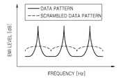
25 is a diagram showing EMI for the output data of Fig.
26 is a view showing a display driving integrated circuit according to an embodiment of the present invention in more detail.
27 is a view illustrating a display module according to an embodiment of the present invention.
28 is a diagram illustrating a display system according to an embodiment of the present invention.
29 is a view showing an application example of various electronic products on which a display device according to an embodiment of the present invention is mounted.
30 is a flowchart showing an operation method of a display driving integrated circuit according to an embodiment of the present invention.
이하, 첨부한 도면을 참조하여 본 발명의 실시 예에 대해 상세히 설명한다. 본 발명의 실시 예는 당 업계에서 평균적인 지식을 가진 자에게 본 발명을 보다 완전하게 설명하기 위하여 제공되는 것이다. 본 발명은 다양한 변경을 가할 수 있고 여러 가지 형태를 가질 수 있는 바, 특정 실시 예들을 도면에 예시하고 상세하게 설명하고자 한다. 그러나, 이는 본 발명을 특정한 개시 형태에 대해 한정하려는 것이 아니며, 본 발명의 사상 및 기술 범위에 포함되는 모든 변경, 균등물 내지 대체물을 포함하는 것으로 이해되어야 한다. 각 도면을 설명하면서 유사한 참조부호를 유사한 구성요소에 대해 사용한다. 첨부된 도면에 있어서, 구조물들의 치수는 본 발명의 명확성을 기하기 위하여 실제보다 확대하거나 축소하여 도시한 것이다.Hereinafter, embodiments of the present invention will be described in detail with reference to the accompanying drawings. Embodiments of the present invention are provided to more fully describe the present invention to those skilled in the art. The present invention is capable of various modifications and various forms, and specific embodiments are illustrated and described in detail in the drawings. It should be understood, however, that the invention is not intended to be limited to the particular forms disclosed, but on the contrary, is intended to cover all modifications, equivalents, and alternatives falling within the spirit and scope of the invention. Like reference numerals are used for similar elements in describing each drawing. In the accompanying drawings, the dimensions of the structures are enlarged or reduced from the actual dimensions for the sake of clarity of the present invention.
본 출원에서 사용한 용어는 단지 특정한 실시 예를 설명하기 위해 사용된 것으로, 본 발명을 한정하려는 의도가 아니다. 단수의 표현은 문맥상 명백하게 다르게 뜻하지 않는 한, 복수의 표현을 포함한다. 본 출원에서, "포함하다" 또는 "가지다" 등의 용어는 명세서 상에 기재된 특징, 숫자, 단계, 동작, 구성요소, 부분품 또는 이들을 조합한 것이 존재함을 지정하려는 것이지, 하나 또는 그 이상의 다른 특징들이나 숫자, 단계, 동작, 구성 요소, 부분품 또는 이들을 조합한 것들의 존재 또는 부가 가능성을 미리 배제하지 않는 것으로 이해되어야 한다.The terminology used in this application is used only to describe a specific embodiment and is not intended to limit the invention. The singular expressions include plural expressions unless the context clearly dictates otherwise. In this application, the terms "comprises", "having", and the like are used to specify that a feature, a number, a step, an operation, an element, a part or a combination thereof is described in the specification, But do not preclude the presence or addition of one or more other features, integers, steps, operations, components, parts, or combinations thereof.
다르게 정의되지 않는 한, 기술적이거나 과학적인 용어를 포함해서 여기서 사용되는 모든 용어들은 본 발명이 속하는 기술 분야에서 통상의 지식을 가진 자에 의해 일반적으로 이해되는 것과 동일한 의미를 갖는다. 일반적으로 사용되는 사전에 정의되어 있는 것과 같은 용어들은 관련 기술의 문맥상 가지는 의미와 일치하는 의미를 가지는 것으로 해석되어야 하며, 본 출원에서 명백하게 정의하지 한, 이상적이거나 과도하게 형식적인 의미로 해석되지 않는다.Unless otherwise defined, all terms used herein, including technical or scientific terms, have the same meaning as commonly understood by one of ordinary skill in the art to which this invention belongs. Terms such as those defined in commonly used dictionaries are to be construed to have meanings consistent with the contextual meanings of the related art and are not to be construed as ideal or overly formal meanings as are expressly defined in the present application .
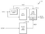
도 1은 본 발명의 일 실시예에 따른 디스플레이 구동 집적회로를 나타내는 도면이다. 도 1을 참조하면, 디스플레이 구동 집적회로(100)는 타이밍 컨트롤러(120) 및 소스 구동부(140)를 포함한다. 타이밍 컨트롤러(120)는 입력되는 입력 데이터를 처리하여 출력 데이터로 출력한다. 타이밍 컨트롤러(120)는 데이터 선택부(122), 데이터 난수화부(124) 및 데이터 전송부(126)를 포함한다.1 is a diagram illustrating a display driving integrated circuit according to an embodiment of the present invention. Referring to FIG. 1, the
데이터 선택부(122)는 입력 데이터(IDTA) 및 인코디드 데이터(EDTA) 중 하나를 선택 데이터(SDTA)로 선택한다. 데이터 선택부(122)는 입력 데이터(IDTA) 및 인코디드 데이터(EDTA)의 천이 개수를 비교하여, 선택 데이터(SDTA)를 선택한다. 선택 데이터(SDTA)는 데이터 난수화부(124)로 전송된다. 데이터 난수화부(124)는 선택 데이터(SDTA)를 난수화하여 난수 데이터(RDTA)로 생성한다. 데이터 전송부(126)는 난수 데이터(RDTA)를 출력 데이터(ODTA)로 변환한다. 데이터 선택부(122), 데이터 난수화부(124) 및 데이터 전송부(126)의 구체적인 동작은 후술된다.The
소스 구동부(140)는 타이밍 컨트롤러(120)와 연결되는 전송 채널(CH)을 통해 입력되는 출력 데이터(ODTA)를 아날로그 변환하여 디스플레이 데이터(DDTA)로 출력한다.The
도 1의 디스플레이 구동 집적회로는 디스플레이 장치에 포함될 수 있다. 도 2는 도 1의 디스플레이 구동 집적회로를 포함하는 디스플레이 장치의 일 예를 나타내는 도면이다.The display drive integrated circuit of Fig. 1 may be included in a display device. 2 is a diagram showing an example of a display device including the display driving integrated circuit of FIG.
도 2를 참조하면, 디스플레이 장치(1000)는 영상(디스플레이 데이터)을 표시하는 디스플레이 패널(200)과, 디스플레이 패널(200)을 구동하기 위한 디스플레이 구동 집적회로(100)를 구비한다. 디스플레이 구동 집적회로(100)는 도 1의 타이밍 컨트롤러(120) 및 소스 구동부(140)를 포함한다. 디스플레이 구동 집적회로(100)는 또한, 게이트 구동부(160) 및 전압 생성부(180)를 더 포함할 수 있다. 소스 구동부(140) 및 게이트 구동부(160)는, 각각, 소스 드라이버 및 게이트 드라이버를 적어도 하나 이상 구비할 수 있다. 이하에서는 소스 구동부(140) 및 게이트 구동부(160)의 동작을, 각각, 소스 드라이버 및 게이트 드라이버의 동작과 혼용되어 기술될 수 있다.2, the
타이밍 컨트롤러(120)는 소스 구동부(140) 및 게이트 구동부(160)를 구동하기 위한 각종 타이밍 신호나 데이터(RGB DATA, CONT1, CONT2)를 발생한다. 타이밍 컨트롤러(120)가 소스 구동부(140)로 전달하는 데이터(RGB DATA)는 도 1의 디스플레이 데이터(DDTA)일 수 있다. 타이밍 컨트롤러(120)는 외부 장치(예를 들어, 호스트 장치(미도시))로부터 외부 데이터(I_DATA), 수평 동기 신호(H_SYNC), 수직 동기 신호(V_SYNC), 클럭 신호(MCLK) 및 데이터 인에이블 신호(DE)를 입력받는다. 외부 데이터(I_DATA)는 도 1의 입력 데이터(IDTA)일 수 있다.The
타이밍 컨트롤러(120)는 외부 데이터(I_DATA)를, 소스 구동부(140)와의 인터페이스 사양에 맞도록 포맷(format)을 변환한 픽셀 데이터(RGB DATA)로 생성하고 이를 소스 구동부(140)에 전송한다. 또한, 타이밍 컨트롤러(1400)는 소스 드라이버(1200) 및 게이트 드라이버(1300)의 타이밍을 제어하기 위해 수평 동기 신호(H_SYNC), 수직 동기 신호(V_SYNC), 클럭 신호(MCLK) 및 데이터 인에이블 신호(DE)에 근거하여, 적어도 하나 이상의 제1 타이밍 제어 신호(CONT1)를 소스 구동부(140)로 출력하고 적어도 하나 이상의 제2 타이밍 제어 신호(CONT2)를 게이트 구동부(160)로 출력한다.The
도 3은 도 2의 디스플레이 패널에 대한 타이밍 제어 신호들의 예를 나타내는 도면이다. 도 3을 참조하면, 디스플레이 패널(200)은 예를 들어, 액정 표시(liquid crystal display, LCD) 패널일 수 있다. 디스플레이 패널(200)에 디스플레이 되는 영역(visible area)에 디스플레이 되는 데이터는 프레임(frame)이라 명명될 수 있다. 예를 들어, 60 Hz로 디스플레이 패널(200)이 구동된다면, 1초에 60장의 프레임이 디스플레이 패널(200)에 디스플레이 된다. 프레임은 수평 방향의 수평 라인(예를 들어, y번째 라인)을 포함할 수 있다.3 is a diagram showing an example of timing control signals for the display panel of FIG. Referring to FIG. 3, the
제1 타이밍 제어 신호(CONT1) 및 제2 타이밍 제어 신호(CONT2)는 디스플레이 되는 영역에 프레임이 정확하게 디스플레이 되도록 타이밍을 조절한다. 예를 들어, 제1 타이밍 제어 신호(CONT1) 및 제2 타이밍 제어 신호(CONT2)는 수평 동기 신호(horizontal synch pulse), 수직 동기 신호(vertical synch pulse), 프론트 포치(front porch) 및 백 포치(back porch) 등일 수 있다.The first timing control signal CONT1 and the second timing control signal CONT2 adjust the timing so that the frame is correctly displayed in the displayed area. For example, the first timing control signal CONT1 and the second timing control signal CONT2 may be a horizontal synchronous signal, a vertical synch pulse, a front porch, and a back porch back porch).
수평 동기 신호(horizontal synch pulse)는 수평 라인마다 인가된다. 하나의 프레임에 대한 모든 수평 라인에 대한 디스플레이가 수행되면, 수직 동기 신호(vertical synch pulse)가 인가되어, 새로운 프레임이 디스플레이 될 수 있다. 또한, 프론트 포치(front porch) 및 백 포치(back porch)는 일종의 마진 역할을 할 수 있다. 예를 들어, 하나의 수평 라인을 디스플레이 하려면, 하나의 클럭 길이의 수평 동기 신호가 디스플레이 패널(200)에 인가되고, 다음으로 백 포치에 해당하는 임의의 개수의 클럭이 인가된 이후에 수평 라인에 해당하는 데이터가 디스플레이 될 수 있다. 하나의 수평 라인에 대한 디스플레이가 완료되면, 프론트 포치에 해당하는 임의의 개수의 클럭이 인가된 이후에 다음 수평 라인에 대한 수평 동기 신호가 인가될 수 있다.A horizontal synch pulse is applied to each horizontal line. When display is performed for all the horizontal lines for one frame, a vertical synch pulse is applied and a new frame can be displayed. Also, the front porch and the back porch can serve as a kind of margin. For example, in order to display one horizontal line, a horizontal synchronizing signal of one clock length is applied to the
다시 도 2를 참조하면, 소스 구동부(140)는 타이밍 컨트롤러(120)로부터 타이밍 신호나 데이터(CONT1, RGB DATA)를 수신하여 디스플레이 패널(200)의 데이터 라인(DL1~DLm)을 구동한다. 게이트 구동부(160)는 타이밍 컨트롤러(120)로부터 타이밍 신호(CONT2)를 수신하여 디스플레이 패널(200)의 게이트 라인(GL1~GLn)을 구동한다.2, the
전압 생성부(180)는 디스플레이 패널(200)의 구동에 필요한 각종 전압들(VON, VOFF, AVDD, VCOM)을 발생시킬 수 있다. 예를 들어, 전압 생성부(180)는 외부로부터 전원 전압(VDD)을 입력 받아, 게이트 온 전압(VON), 게이트 오프 전압(VOFF)을 발생하여 게이트 구동부(160)로 인가하고, 아날로그 전원 전압(AVDD), 공통 전압(VCOM)을 발생하여 소스 구동부(140)로 인가할 수 있다.The
디스플레이 장치(1000)는 각종 평판 디스플레이 장치 중 어느 하나가 적용될 수 있다. 예를 들어, 평판 디스플레이 장치는 액정 표시(liquid crystal display, LCD) 장치, 유기 EL(electro luminance) 표시 장치, PDP(plasma display panel) 장치 등일 수 있고, 본 발명의 실시예에 따른 디스플레이 장치(1000)는 이들 장치 중 어느 하나가 적용될 수 있다. 또는 평판 디스플레이 장치는 물리적 터치 또는 광 터치를 센싱할 수 있는 평판 디스플레이 장치일 수 있고, 본 발명의 실시예에 따른 디스플레이 장치(1000)는 그러한 하이브리드 평판 디스플레이 장치가 적용될 수 있다. 설명의 편의상, 아래에서는 본 발명을 설명함에 있어서 액정 표시 장치를 예로 들어 설명한다.The
디스플레이 패널(200)은 복수의 게이트 라인(GL1-GLn)과, 게이트 라인들과 교차하는 방향으로 배치되는 복수의 데이터 라인(DL1~DLm)과, 게이트 라인 및 데이터 라인이 교차하는 영역에 배열된 픽셀들(PX)을 포함한다. 디스플레이 장치(1000)가 박막 트랜지스터(Thin Film Transistor, TFT) 액정 디스플레이 장치인 경우, 각 픽셀은 게이트 라인(GL1-GLn)과 데이터 라인(DL1~DLm)에 게이트 전극 및 소스 전극이 각각 연결되는 박막 트랜지스터와, 박막 트랜지스터의 드레인 전극에 연결되는 액정 커패시터 및 스토리지 커패시터를 포함한다(이상, 미도시).The
이러한 픽셀 구조에서는, 게이트 라인이 선택되면 선택된 게이트 라인에 연결된 픽셀의 박막 트랜지스터가 턴 온되고, 이어서 소스 구동부(140)에 의해 각 데이터 라인에 픽셀 정보를 포함하는 데이터 신호가 인가된다. 데이터 신호(예를 들어, 도 1의 디스플레이 데이터(DDTA))는 해당 픽셀의 박막 트랜지스터를 거쳐 액정 커패시터와 스토리지 커패시터에 인가되며, 액정 및 스토리지 커패시터들이 구동됨으로써 디스플레이 동작이 이루어진다.In this pixel structure, when a gate line is selected, a thin film transistor of a pixel connected to a selected gate line is turned on, and then a data signal including pixel information is applied to each data line by the
디스플레이 구동 집적회로(100)에서 구동해야 하는 디스플레이 패널(200)의 픽셀(PX)의 개수가 많아짐에 따라, 소스 구동부(140)는 다수의 소스 드라이버를 구비하고, 각 소스 드라이버는 디스플레이 패널(200)의 대응되는 영역의 소스 라인을 구동할 수 있다.As the number of pixels PX of the
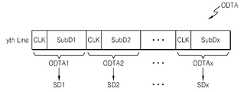
도 4는 도 1의 소스 구동부의 일 예를 나타내는 도면이다. 도 4를 참조하면, 소스 구동부(140)는 x(x는 2 이상의 양의 정수)개의 소스 드라이버(SD1, SD2, … SDx)를 포함할 수 있다. x개의 소스 드라이버(SD1, SD2, … SDx)는 각각, 전술된 소스 구동부(140)의 기능을 수행한다. 구체적으로, x개의 소스 드라이버(SD1, SD2, … SDx)는 각각, 전술된 디스플레이 데이터(DDTA)를 디스플레이 패널(200)에 전송함에 있어서, 타이밍 컨트롤러(120)로부터 각각, 대응되는 출력 데이터(ODTA1, ODTA2, … ODTAx)를 수신하고, 수신되는 출력 데이터(ODTA1, ODTA2, … ODTAx)를 아날로그 전압으로 디코딩하며, 디코딩 결과에 따라 복수의 계조 전압 중 하나의 계조 전압을 선택하여, 디스플레이 패널(200)에 디스플레이 데이터(DDTA1, DDTA2, … DDTA x)로 인가할 수 있다.4 is a diagram showing an example of the source driver of FIG. Referring to FIG. 4, the
x개의 소스 드라이버(SD1, SD2, … SDx)는 각각, 타이밍 컨트롤러(120)와 포인트-투-포인트(point-to-point)로 연결될 수 있다. 예를 들어, 제1 소스 드라이버(SD1)는 타이밍 컨트롤러(120)와 제1 전송 채널(CH1)로 연결되고, 제2 소스 드라이버(SD2)는 타이밍 컨트롤러(120)와 제2 전송 채널(CH1)로 연결될 수 있다. 마찬가지로, 제x 소스 드라이버(SDx)는 타이밍 컨트롤러(120)와 제x 전송 채널(CHx)로 연결될 수 있다. 도 4에 도시되지 아니하였으나, 도 2의 타이밍 제어 신호(CONT1, CONT2) 중 전부 또는 일부는 전송 채널(CH1, CH2, … CHx)과 별도로 구비되고, x개의 소스 드라이버(SD1, SD2, … SDx) 모두에 연결되는 채널을 통해 x개의 소스 드라이버(SD1, SD2, … SDx)에 연결될 수도 있다.Each of the x source drivers SD1, SD2, ... SDx may be connected to the
x개의 소스 드라이버(SD1, SD2, … SDx)는 각각, 대응되는 전송 채널(CH1, CH2, … CHx)로 인가되는 출력 데이터(ODTA1, ODTA2, … ODTAx)를 수신한다. 예를 들어, 제1 소스 드라이버(SD1)는 제1 전송 채널(CH1)로 인가되는 제1 출력 데이터(ODTA1)를 수신하고, 제2 소스 드라이버(SD2)는 제2 전송 채널(CH1)로 인가되는 제2 출력 데이터(ODTA2)를 수신할 수 있다. 마찬가지로, 제x 소스 드라이버(SDx)는 제x 전송 채널(CHx)로 인가되는 제x 출력 데이터(ODTAx)를 수신할 수 있다. 전술한 바와 같이, 출력 데이터(ODTA1, ODTA2, … ODTAx)는 타이밍 컨트롤러(120)에 의해, 입력 데이터(IDTA)가 처리된 데이터이다. 입력 데이터(IDTA) 및 출력 데이터(ODTA1, ODTA2, … ODTAx)는 각각, 개념적으로 도 5 및 도 6과 같이 나타내어 질 수 있다.The x source drivers SD1, SD2, ... SDx receive the output data ODTA1, ODTA2, ..., ODTAx applied to the corresponding transfer channels CH1, CH2, ... CHx, respectively. For example, the first source driver SD1 receives the first output data ODTA1 applied to the first transmission channel CH1 and the second source driver SD2 receives the first output data ODTA1 applied to the second transmission channel CH1 The second output data ODTA2 can be received. Similarly, the x-th source driver SDx can receive the x-th output data ODTAx applied to the x-th transfer channel CHx. As described above, the output data ODTA1, ODTA2, ... ODTAx are the data processed by the
도 5는 본 발명의 일 실시예에 따른 입력 데이터의 예를 개념적으로 나타낸 도면이고, 도 6은 본 발명의 일 실시예에 따른 출력 데이터의 예를 개념적으로 나타낸 도면이다. 먼저, 도 5를 참조하면, 입력 데이터(IDTA)는 도 2 내지 도 4의 디스플레이 패널(200)의 수평 라인(게이트 라인)에 대응되는 크기로 입력될 수 있다. 예를 들어, 입력 데이터(IDTA)는 디스플레이 패널(200)의 수평 라인(예를 들어, 도 3의 프레임의 y번째 라인)과 동일한 크기(L)로 입력될 수 있다.FIG. 5 conceptually shows an example of input data according to an embodiment of the present invention, and FIG. 6 conceptually shows an example of output data according to an embodiment of the present invention. 5, the input data IDTA may be input in a size corresponding to the horizontal line (gate line) of the
이 경우, 소스 구동부(140)가 x개의 소스 드라이버(SD1, SD2, … SDx)를 포함하면, x개의 소스 드라이버(SD1, SD2, … SDx) 각각은, 입력 데이터(IDTA)를 x개로 나눈 단위(T=L/x)에 대응되는 도 6의 출력 데이터(ODTA1, ODTA2, … ODTAx)를 수신할 수 있다. 도 1 또는 도 4의 타이밍 컨트롤러(120)는 입력 데이터(IDTA)를 x개로 나눈 x개의 서브 데이터(SubD1, SubD2, … SubDx)마다 클럭(CLK)을 임베디드(embedded)할 수 있다. 예를 들어, 입력 데이터(IDTA)를 x개로 나눈 단위를 제1 서브 데이터(SubD1), 제2 서브 데이터(SubD2) 내지 제x 서브 데이터(SubDx)로 나타내면, 제1 서브 데이터(SubD1), 제2 서브 데이터(SubD2) 내지 제x 서브 데이터(SubDx) 각각에 클럭(CLK)이 포함될 수 있다. 예를 들어, 제1 서브 데이터(SubD1)와 제1 서브 데이터(SubD1)에 대한 클럭(CLK)이 제1 출력 데이터(ODTA)로 제1 소스 드라이버(SD1)에 전송되고, 제2 서브 데이터(SubD2)와 제2 서브 데이터(SubD2)에 대한 클럭(CLK)이 제2 출력 데이터(ODTA)로 제2 소스 드라이버(SD2)에 전송될 수 있다. 마찬가지로, 제x 서브 데이터(SubDx)와 제x 서브 데이터(SubDx)에 대한 클럭(CLK)이 제x 출력 데이터(ODTA)로 제x 소스 드라이버(SDx)에 전송될 수 있다. 다만, 제1 출력 데이터(ODTA) 내지 제x 출력 데이터(ODTA)는 헤더(header) 등이 더 포함될 수 있고, 이는 후술된다.In this case, when the
다시 도 4를 참조하면, x개의 소스 드라이버(SD1, SD2, … SDx)는 각각, 수신된 출력 데이터(ODTA1, ODTA2, … ODTAx)를 처리하여 대응되는 디스플레이 데이터(DDTA)로 출력한다. 예를 들어, 제1 소스 드라이버(SD1)는 제1 전송 채널(CH1)로 인가되는 제1 출력 데이터(ODTA)를 처리하여 제1 디스플레이 데이터(DDTA)로 출력하고, 제2 소스 드라이버(SD2)는 제2 전송 채널(CH1)로 인가되는 제2 출력 데이터(ODTA)를 처리하여 제2 디스플레이 데이터(DDTA)로 출력할 수 있다. 마찬가지로, 제x 소스 드라이버(SDx)는 제x 전송 채널(CHx)로 인가되는 제x 출력 데이터(ODTA)를 처리하여 제x 디스플레이 데이터(DDTA)로 출력할 수 있다. 전술한 바와 같이, x개의 소스 드라이버(SD1, SD2, … SDx)는 각각, 도 3의 디스플레이 패널(200)의 프레임의 대응되는 영역을 구동할 수 있다. 예를 들어, 제1 소스 드라이버(SD1)는 제1 디스플레이 데이터(DDTA1)를 수평 라인을 x로 나눈 첫 번째 영역에 디스플레이 시키고, 제2 소스 드라이버(SD2)는 제2 디스플레이 데이터(DDTA2)를 수평 라인을 x로 나눈 두 번째 영역에 디스플레이 시킬 수 있다. 마찬가지로, 제x 소스 드라이버(SDx)는 제x 디스플레이 데이터(DDTAx)를 수평 라인을 x로 나눈 마지막 영역에 디스플레이 시킬 수 있다.Referring again to FIG. 4, each of the x source drivers SD1, SD2, ... SDx processes the received output data ODTA1, ODTA2, ... ODTAx and outputs the processed output data DDTA. For example, the first source driver SD1 processes the first output data ODTA applied to the first transmission channel CH1 and outputs the first output data ODTA to the first display data DDTA, May process the second output data ODTA applied to the second transmission channel CH1 and output the second output data ODTA to the second display data DDTA. Similarly, the xth source driver SDx may process the xth output data ODTA applied to the xth transfer channel CHx and output it as the x th display data DDTA. As described above, each of the x source drivers SD1, SD2, ..., SDx can drive a corresponding region of the frame of the
도 7은 본 발명의 일 실시예에 따른 타이밍 컨트롤러 및 소스 구동부 사이의 인터페이스의 예를 나타내는 도면이다. 전술한 바와 같이, 타이밍 컨트롤러(120) 및 x개의 각 소스 드라이버(SD1, SD2, … SDx)는 각각, 포인트-투-포인트 방식으로 전송 채널(CH1, CH2, … CHx)이 연결될 수 있다. 또한, 각 전송 채널(CH1, CH2, … CHx)을 통해 클럭(CLK)이 포함된 출력 데이터(ODTA1, ODTA2, … ODTAx)가 x개의 소스 드라이버(SD1, SD2, … SDx) 각각으로 전송될 수 있다. 예를 들어, 타이밍 컨트롤러(120)의 데이터 전송부(126) 및 x개의 각 소스 드라이버(SD1, SD2, … SDx)는 각각, 두 개의 전송 채널(CH1a, CH1b)로 연결되어, eRVDS(enhanced Reduced Voltage Differential Signaling) 인터페이스를 통해 출력 데이터(ODTA1, ODTA2, … ODTAx)를 수신할 수 있다.7 is a diagram illustrating an example of an interface between a timing controller and a source driver according to an embodiment of the present invention. As described above, the
도 7은 제1 소스 드라이버(SD1)의 예에 한하여 도시하였으나, 다른 소스 드라이버도 동일하게 두 개의 전송 채널(CH1a, CH1b)로 연결될 수 있다. 두 개의 전송 채널(CH1a, CH1b)은 각각, 인접한 수평 라인에 대한 출력 데이터를 전송할 수 있다. 다만, 타이밍 컨트롤러(120)와 x개의 소스 드라이버(SD1, SD2, … SDx) 각각은 eRVDS 인터페이스가 아닌, 클럭이 임베디드 되는 다른 인트라 패널 인터페이스(intra-panel interface)에 의해 연결될 수도 있다. 예를 들어, 멀티 드롭(multi-drop) 방식의 인터페이스에 의해 타이밍 컨트롤러(120)와 x개의 소스 드라이버(SD1, SD2, … SDx)가 연결될 수도 있다.Although FIG. 7 shows only the example of the first source driver SD1, other source drivers may be connected to the same two transfer channels CH1a and CH1b. The two transmission channels (CH1a, CH1b) can each transmit output data for adjacent horizontal lines. Each of the
다시 도 1을 참조하면, 본 발명의 일 실시예에 따른 디스플레이 구동 집적회로(100)는 타이밍 컨트롤러(120)에서 소비되는 전력을 줄이기 위해, 데이터 선택부(122)는 입력 데이터(IDTA), 및 입력 데이터(IDTA)를 인코딩한 인코디드 데이터(EDTA) 중 천이 개수가 적은 데이터를 선택한다.1, the
도 8은 도 1의 데이터 선택부의 일 예를 나타내는 도면이다. 도 8을 참조하면, 데이터 선택부(122)는 데이터 입력부(122_1), 제1 천이 산출부(122_2), 데이터 인코딩부(122_3), 제2 천이 산출부(122_4), 비교부(122_5) 및 데이터 출력부(122_6)를 포함할 수 있다. 데이터 입력부(122_1)로 입력 데이터(IDTA)가 입력될 수 있다. 제1 천이 산출부(122_2)는 입력 데이터(IDTA)의 천이 개수를 제1 값(VAL1)으로 산출할 수 있다.8 is a diagram showing an example of the data selector of FIG. 8, the
도 9는 본 발명의 일 실시예에 따른 입력 데이터에서의 천이 개수를 산출하는 예를 나타내는 도면이다. 전술한 바와 같이, 입력 데이터(IDTA)는 프레임의 수평 라인(yth Line) 단위로 입력될 수 있어, 입력 데이터(IDTA)는 프레임의 수평 라인의 연속된 픽셀에 대한 픽셀 데이터를 포함할 수 있다. 도 9는 입력 데이터(IDTA)에 연속하는 M개의 픽셀 데이터(P_1st, P_2nd, … P_Mth)가 포함된 예를 도시한다. 입력 데이터(IDTA)의 천이 개수는 입력 데이터(IDTA)의 인접한 픽셀 데이터의 대응되는 비트의 비트 값(논리 값)이 다른, 비트의 개수일 수 있다. 제1 천이 산출부(122_2)는 입력 데이터(IDTA)의 연속된 첫 번째 픽셀 데이터(P_1st) 내지 M 번째 픽셀 데이터(P_MTH) 중 인접한 픽셀 데이터를 각각 배타적 논리합한 값들에서 1의 개수를 카운트한 값을 제1 값(VAL1)으로 산출할 수 있다.9 is a diagram showing an example of calculating the number of transitions in input data according to an embodiment of the present invention. As described above, the input data IDTA can be input in units of a horizontal line (yth Line) of the frame, and the input data IDTA can include pixel data for successive pixels of the horizontal line of the frame. FIG. 9 shows an example in which M pixel data (P_1st, P_2nd, ..., P_Mth) continuous to the input data IDTA are included. The number of transitions of the input data IDTA may be the number of bits different from the bit value (logical value) of the corresponding bit of the adjacent pixel data of the input data IDTA. The first transition calculator 122_2 counts the number of 1's obtained by XORing adjacent pixel data among consecutive first pixel data P_1st to Mth pixel data P_MTH of the input data IDTA Can be calculated as the first value (VAL1).
예를 들어, 제1 천이 산출부(122_2)는 첫 번째 픽셀 데이터(P_1st)에서 1의 개수를 카운트하고, 첫 번째 픽셀 데이터(P_1st)와 두 번째 픽셀 데이터(P_2nd)를 배타적 논리합한 결과에서 1의 개수를 카운트하며, 두 번째 픽셀 데이터(P_2nd)와 세 번째 픽셀 데이터(P_3rd)를 배타적 논리합한 결과에서 1의 개수를 카운트할 수 있다. 제1 천이 산출부(122_2)는 같은 방식으로 M-1 번째 픽셀 데이터(P_M-1TH)와 M 번째 픽셀 데이터(P_MTH)를 배타적 논리합할 때까지, 인접한 픽셀 데이터는 배타적 논리합하고 배타적 논리합한 결과에서 1의 개수를 카운트한다. 카운트된 1의 개수를 총합하여, 입력 데이터(IDTA)의 천이 개수가 제1 값(VAL1)으로 산출될 수 있다.For example, the first transition calculator 122_2 counts the number of 1's in the first pixel data P_1st, and
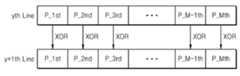
도 10은 본 발명의 다른 실시예에 따른 입력 데이터에서의 천이 개수를 산출하는 예를 나타내는 도면이다. 도 8 및 도 10을 참조하면, 프레임의 수평 라인 단위로 입력되는 입력 데이터(IDTA)의 천이 개수는 연속하는 수평 라인에 대한 입력 데이터(IDTA)의 대응되는 픽셀 데이터의 대응되는 비트의 비트 값(논리 값)이 다른, 비트의 개수일 수 있다. 예를 들어, 제1 천이 산출부(122_2)는 연속하는 수평 라인(yth Line 및 y+1th Line)에 대한 입력 데이터(IDTA)들의 첫 번째 픽셀 데이터(P_1st)를 배타적 논리합한 값에서 1의 개수를 카운트하고, 연속하는 수평 라인(yth Line 및 y+1th Line)에 대한 입력 데이터(IDTA)들의 두 번째 픽셀 데이터(P_2nd)를 배타적 논리합한 값에서 1의 개수를 카운트할 수 있다. 제1 천이 산출부(122_2)는 같은 방식으로 연속하는 수평 라인(yth Line 및 y+1th Line)에 대한 입력 데이터(IDTA)의 M 번째 픽셀 데이터(P_MTH)까지 배타적 논리합한 결과에서 1의 개수를 카운트한다.10 is a diagram showing an example of calculating the number of transitions in input data according to another embodiment of the present invention. 8 and 10, the number of transitions of the input data IDTA input in the horizontal line unit of the frame is the bit value of the corresponding bit of the corresponding pixel data of the input data IDTA for the continuous horizontal line Logical value) may be different, the number of bits. For example, the first transition calculator 122_2 calculates the number of 1's by the exclusive-OR of the first pixel data P_1st of the input data IDTA for the consecutive horizontal lines yth Line and y + 1th Line And the number of 1's can be counted by exclusive-ORing the second pixel data P_2nd of the input data IDTA with respect to the continuous horizontal lines (yth Line and y + 1th Line). The first transition calculator 122_2 calculates the number of 1's by the exclusive-OR operation on the M-th pixel data P_MTH of the input data IDTA for the horizontal lines (yth Line and y + 1th Line) Count.
제1 천이 산출부(122_2)는 연속하는 수평 라인(yth Line 및 y+1th Line)의 대응되는 픽셀 데이터들을 배타적 논리합한 결과에서 카운트된 1의 개수를 총합하여 입력 데이터(IDTA)의 천이 개수로서 제1 값(VAL1)을 산출할 수 있다. 도 10과 같이 연속하는 수평 라인(yth Line 및 y+1th Line) 사이의 차이를 산출하기 위해서는, 도 8의 데이터 입력부(122_1)는 도 9의 경우에 대응되는 데이터 입력부(122_1)보다 2배의 크기로 구비될 수 있다.The first transition calculator 122_2 totals the number of 1's counted in the result of the exclusive-OR operation of the corresponding pixel data of the consecutive horizontal lines (yth Line and y + 1th Line) to obtain the number of transitions of the input data IDTA The first value VAL1 can be calculated. In order to calculate the difference between successive horizontal lines (yth Line and y + 1th Line) as shown in Fig. 10, the data input unit 122_1 of Fig. 8 has twice the data input unit 122_1 Size.
다시 도 8을 참조하면, 데이터 인코딩부(122_3)는 입력 데이터(IDTA)를 인코디드 데이터(EDTA)로 인코딩(encoding)할 수 있다. 그리고, 제2 천이 산출부(122_4)는 인코디드 데이터(EDTA)의 천이 개수를 제2 값(VAL2)으로 산출할 수 있다.Referring again to FIG. 8, the data encoding unit 122_3 may encode the input data IDTA with the encoded data EDTA. The second transition calculator 122_4 can calculate the number of transitions of the encoded data EDTA as the second value VAL2.
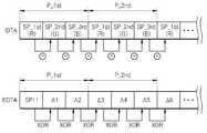
도 11은 본 발명의 일 실시예에 따른 인코디드 데이터 및 인코디드 데이터에서의 천이 개수를 산출하는 예를 나타내는 도면이다. 도 8 및 도 11을 참조하면, 데이터 인코딩부(122_3)는, 입력 데이터(IDTA)의 연속된 첫 번째 픽셀 데이터(P_1st) 내지 M 번째 픽셀 데이터(P_MTH)를, 입력 데이터(IDTA)의 첫 번째 픽셀 데이터(P_1st) 및 입력 데이터(IDTA)의 연속된 첫 번째 픽셀 데이터(P_1st) 내지 M 번째 픽셀 데이터(P_MTH) 중 인접한 픽셀 데이터 각각의 차이로 인코딩하여 인코디드 데이터(EDTA)를 생성할 수 있다. 예를 들어, 인코디드 데이터(EDTA)는 입력 데이터(IDTA)의 첫 번째 픽셀 데이터(P_1st), 입력 데이터(IDTA)의 첫 번째 픽셀 데이터(P_1st)와 두 번째 픽셀 데이터(P_2nd)의 차이(△1), 입력 데이터(IDTA)의 두 번째 픽셀 데이터(P_2nd)와 세 번째 픽셀 데이터(P_3rd)의 차이(△2) 내지 입력 데이터(IDTA)의 M-1 번째 픽셀 데이터(P_M-1TH)와 M 번째 픽셀 데이터(P_MTH)의 차이(△M-1)로 인코딩 될 수 있다. 다시 말해, 인코디드 데이터(EDTA)의 첫 번째 픽셀 데이터가 입력 데이터(IDTA)의 첫 번째 픽셀 데이터(P_1st)이고, 인코디드 데이터(EDTA)의 두 번째 픽셀 데이터가 입력 데이터(IDTA)의 첫 번째 픽셀 데이터(P_1st)와 두 번째 픽셀 데이터(P_2nd)의 차이(△1)이며, 인코디드 데이터(EDTA)의 세 번째 픽셀 데이터가 입력 데이터(IDTA)의 두 번째 픽셀 데이터(P_2nd)와 세 번째 픽셀 데이터(P_3rd)의 차이(△2)일 수 있다. 같은 방식으로, 인코디드 데이터(EDTA)의 M 번째 픽셀 데이터가 입력 데이터(IDTA)의 M-1 번째 픽셀 데이터(P_M-1TH)와 M 번째 픽셀 데이터(P_MTH)의 차이(△M-1)일 수 있다. 이때, 인접한 픽셀 데이터의 차이는 뺄셈, 배타적 논리합 그리고 배타적 부정 논리합 등을 이용하여 연산될 수 있다. 뺄셈, 배타적 논리합 그리고 배타적 부정 논리합 중 연산을 구현하는 회로의 크기 등이 고려되어 선택될 수 있다.11 is a diagram showing an example of calculating the number of transitions in the encoded data and the encoded data according to an embodiment of the present invention. Referring to FIGS. 8 and 11, the data encoding unit 122_3 converts the first consecutive pixel data P_1st through Mth pixel data P_MTH of the input data IDTA into the first It is possible to generate the encoded data EDTA by encoding each of the adjacent pixel data among the first consecutive pixel data P_1st through Mth pixel data P_MTH of the pixel data P_1st and the input data IDTA have. For example, the encoded data EDTA is a difference between the first pixel data P_1st of the input data IDTA and the first pixel data P_1st of the input data IDTA and the second pixel data P_2nd 1) th pixel data P_M-1TH of the input data IDTA to the difference (? 2) between the second pixel data P_2nd of the input data IDTA and the third pixel data P_3rd, May be encoded with the difference (M-1) of the Mth pixel data (P_MTH). In other words, when the first pixel data of the encoded data EDTA is the first pixel data P_1st of the input data IDTA and the second pixel data of the encoded data EDTA is the input data IDTA, Is the difference (? 1) between the first pixel data P_1st and the second pixel data P_2nd and the third pixel data of the encoded data EDTA is the second pixel data P_2nd of the input data IDTA (? 2) of the third pixel data P_3rd. In the same manner, the Mth pixel data of the encoded data EDTA is the difference (DELTA M-1) between the M-1th pixel data P_M-1TH of the input data IDTA and the Mth pixel data P_MTH, Lt; / RTI > At this time, the difference between adjacent pixel data can be calculated using subtraction, exclusive OR, and exclusive NOR. Subtraction, exclusive OR, and the size of the circuit that implements the exclusive OR operation.
이 경우, 제2 천이 산출부(122_4)는 인코디드 데이터(EDTA)의 첫 번째 픽셀 데이터의 1의 개수를 카운트하고, 인코디드 데이터(EDTA)의 첫 번째 픽셀 데이터 및 두 번째 픽셀 데이터를 배타적 논리합한 결과에서 1의 개수를 카운트하고, 인코디드 데이터(EDTA)의 두 번째 픽셀 데이터 및 세 번째 픽셀 데이터를 배타적 논리합한 결과에서 1의 개수를 카운트할 수 있다. 제2 천이 산출부(122_4)는 같은 방식으로 인코디드 데이터(EDTA)의 M-1 번째 픽셀 데이터와 M 번째 픽셀 데이터를 배타적 논리합할 때까지, 인코디드 데이터(EDTA)의 인접한 픽셀 데이터 사이의 차이를 배타적 논리합하고 배타적 논리합한 결과에서 1의 개수를 카운트한다. 카운트된 1의 개수를 총합하여, 인코디드 데이터(EDTA)의 천이 개수가 제2 값(VAL2)으로 산출될 수 있다.In this case, the second transition calculator 122_4 counts the number of 1's of the first pixel data of the encoded data EDTA, and outputs the first pixel data and the second pixel data of the encoded data EDTA The number of 1's is counted from the result of the exclusive-OR, and the number of 1's can be counted in the result of exclusive-ORing the second pixel data and the third pixel data of the incoded data EDTA. The second transition calculator 122_4 calculates the difference between the adjacent pixel data of the encoded data EDTA until the M-1th pixel data of the EDTA is subjected to exclusive OR operation with the Mth pixel data, And the number of 1's is counted in the result of the exclusive-OR operation. The number of counts of 1 can be summed up and the number of transitions of the encoded data EDTA can be calculated as the second value VAL2.
도 12는 본 발명의 다른 실시예에 따른 인코디드 데이터 및 인코디드 데이터에서의 천이 개수를 산출하는 예를 나타내는 도면이다. 도 8 및 도 12를 참조하면, 입력 데이터(IDTA)의 연속된 첫 번째 픽셀 데이터(P_1st) 내지 M 번째 픽셀 데이터(P_MTH) 각각이 연속된 첫 번째 서브 픽셀 데이터(SP_1st) 내지 N 번째 서브 픽셀(SP_3RD)를 포함할 수 있고, 따라서 입력 데이터(IDTA)가 연속된 첫 번째 서브 픽셀 데이터(SP_1st) 내지 M*N 번째 서브 픽셀(SP_3RD)을 포함할 수 있다. 데이터 인코딩부(122_3)는, 입력 데이터(IDTA)의 첫 번째 서브 픽셀 데이터(SP_1st), 및 입력 데이터(IDTA)의 연속된 첫 번째 서브 픽셀 데이터(SP_1st) 내지 M*N 번째 서브 픽셀(SP_3RD) 중 인접한 서브 픽셀 데이터 각각의 차이로 인코딩하여 인코디드 데이터(EDTA)를 생성할 수 있다. 도 12는 각 픽셀 데이터가 R(Red), G(Green) 및 B(Blue)의 3개의 서브 픽셀 데이터를 포함하는 예를 도시한다.12 is a diagram showing an example of calculating the number of transitions in the encoded data and the encoded data according to another embodiment of the present invention. 8 and 12, each of successive first pixel data P_1st to Mth pixel data P_MTH of the input data IDTA is divided into first consecutive subpixel data SP_1st to Nth subpixel SP_3RD), and thus the input data IDTA may include consecutive first sub-pixel data SP_1st to M * Nth sub-pixel SP_3RD. The data encoding unit 122_3 includes first sub pixel data SP_1st of the input data IDTA and first consecutive sub pixel data SP_1st to M * Nth sub pixel SP_3RD of the input data IDTA, The encoded data EDTA can be generated by encoding the difference between adjacent sub-pixel data. Fig. 12 shows an example in which each pixel data includes three subpixel data of R (Red), G (Green) and B (Blue).
예를 들어, 인코디드 데이터(EDTA)는 입력 데이터(IDTA)의 첫 번째 서브 픽셀 데이터(SP_1st), 입력 데이터(IDTA)의 첫 번째 서브 픽셀 데이터(SP_1st)와 두 번째 서브 픽셀 데이터(SP_2nd)의 차이(△1), 입력 데이터(IDTA)의 두 번째 서브 픽셀 데이터(SP_2nd)와 세 번째 서브 픽셀 데이터(SP_3rd)의 차이(△2) 내지 입력 데이터(IDTA)의 M*N-1 번째 서브 픽셀 데이터와 M*N 번째 서브 픽셀 데이터의 차이로 인코딩 될 수 있다. 다시 말해, 인코디드 데이터(EDTA)의 첫 번째 서브 픽셀 데이터가 입력 데이터(IDTA)의 첫 번째 서브 픽셀 데이터(SP_1st)이고, 인코디드 데이터(EDTA)의 두 번째 서브 픽셀 데이터가 입력 데이터(IDTA)의 첫 번째 서브 픽셀 데이터(SP_1st)와 두 번째 서브 번째 픽셀 데이터(SP_2nd)의 차이(△)1이며, 인코디드 데이터(EDTA)의 세 번째 서브 픽셀 데이터가 입력 데이터(IDTA)의 두 번째 서브 픽셀 데이터(SP_2nd)와 세 번째 서브 픽셀 데이터(SP_3rd)의 차이(△2)일 수 있다. 같은 방식으로, 인코디드 데이터(EDTA)의 M*N 번째 서브 픽셀 데이터가 입력 데이터(IDTA)의 M*N-1 번째 서브 픽셀 데이터와 M*N 번째 서브 픽셀 데이터의 차이일 수 있다.For example, the encoded data EDTA includes the first sub pixel data SP_1st of the input data IDTA, the first sub pixel data SP_1st and the second sub pixel data SP_2nd of the input data IDTA, The difference (? 1) between the second sub-pixel data SP_2nd and the third sub-pixel data SP_3rd of the input data IDTA and the M * N-1th sub- Pixel data and the M * Nth sub-pixel data. In other words, when the first sub pixel data of the encoded data EDTA is the first sub pixel data SP_1st of the input data IDTA and the second sub pixel data of the encoded data EDTA is the input data ID The difference (DELTA) between the first sub pixel data SP_1st and the second sub pixel data SP_2nd of the input data IDTA is 1 and the third sub pixel data of the encoded data EDTA is the difference (? 2) between the first sub-pixel data SP_2nd and the third sub-pixel data SP_3rd. In the same manner, the M * Nth sub-pixel data of the encoded data EDTA may be the difference between the M * N-1th sub-pixel data of the input data IDTA and the M * Nth sub-pixel data.
이 경우, 제2 천이 산출부(122_4)는 인코디드 데이터(EDTA)의 첫 번째 서브 픽셀 데이터의 1의 개수를 카운트하고, 인코디드 데이터(EDTA)의 첫 번째 서브 픽셀 데이터 및 두 번째 서브 픽셀 데이터를 배타적 논리합한 결과에서 1의 개수를 카운트하고, 인코디드 데이터(EDTA)의 두 번째 서브 픽셀 데이터 및 세 번째 서브 픽셀 데이터를 배타적 논리합한 결과에서 1의 개수를 카운트할 수 있다. 제2 천이 산출부(122_4)는 같은 방식으로 인코디드 데이터(EDTA)의 M*N-1 번째 서브 픽셀 데이터와 M*N 번째 픽셀 데이터를 배타적 논리합할 때까지, 인코디드 데이터(EDTA)의 인접한 서브 픽셀 데이터 사이의 차이를 배타적 논리합하고 배타적 논리합한 결과에서 1의 개수를 카운트한다. 카운트된 1의 개수를 총합하여, 인코디드 데이터(EDTA)의 천이 개수가 제2 값(VAL2)으로 산출될 수 있다.In this case, the second transition calculator 122_4 counts the number of 1s of the first subpixel data of the incoded data EDTA and outputs the first subpixel data of the encoded data EDTA and the second subpixel data of the second The number of 1's is counted in the result of exclusive-ORing the pixel data, and the number of 1's can be counted in the result of exclusive-ORing the second subpixel data and the third subpixel data of the encoded data EDTA. The second transition calculator 122_4 may output the encoded data EDTA until the M * Nth sub pixel data of the incoded data EDTA and the M * Nth pixel data are subjected to the exclusive OR operation, And the number of 1's is counted in the result of the exclusive-OR operation. The number of counts of 1 can be summed up and the number of transitions of the encoded data EDTA can be calculated as the second value VAL2.
이상에서 설명된 인코딩 방식의 예시에 불과하며, 다른 방식으로 인코디드 데이터(EDTA)가 생성될 수 있다. 다시 도 8을 참조하면, 비교부(122_5)는 제1 값(VAL1) 및 제2 값(VAL2)을 비교하여 비교 결과(CRST)로 출력할 수 있다. 비교 결과(CRST)는 이하에서 제1 모드 정보(XMD1)로 기술될 수 있다. 데이터 출력부(122_6)는 비교 결과(CRST)에 따라, 입력 데이터(IDTA) 및 인코디드 데이터(EDTA) 중 하나를 선택 데이터(SDTA)로 출력한다. 예를 들어, 데이터 출력부(122_6)는 제1 값(VAL1)이 제2 값(VAL2)보다 작으면, 입력 데이터(IDTA)를 선택 데이터(SDTA)로 선택할 수 있다. 반면, 데이터 출력부(122_6)는 제2 값(VAL2)이 제1 값(VAL1)보다 작으면, 인코디드 데이터(EDTA)를 선택 데이터(SDTA)로 선택할 수 있다.It is only an example of the encoding method described above, and the encoded data EDTA may be generated in another manner. Referring again to FIG. 8, the comparator 122_5 may compare the first value VAL1 and the second value VAL2 and output the comparison result as a comparison result (CRST). The comparison result (CRST) may be described below as first mode information (XMD1). The data output unit 122_6 outputs one of the input data IDTA and the encoded data EDTA as the selection data SDTA according to the comparison result CRST. For example, the data output unit 122_6 can select the input data IDTA as the selection data SDTA if the first value VAL1 is smaller than the second value VAL2. On the other hand, the data output unit 122_6 may select the encoded data EDTA as the selection data SDTA if the second value VAL2 is smaller than the first value VAL1.
선택 데이터(SDTA)는 제1 모드 정보(XMD1)를 포함할 수 있다. 제1 모드 정보(XMD1)는 제1 값(VAL1) 및 제2 값(VAL2)을 비교한 결과를 나타내므로, 선택 데이터(SDTA)가 입력 데이터(IDTA)인지 인코디드 데이터(EDTA)인지에 대한 정보를 포함한다. 이렇듯, 일 실시예에 따른 타이밍 컨트롤러(120)는 전송 채널(CH)을 통해 전송하고자 하는 데이터의 천이를 줄임으로써, 전력 소모를 줄일 수 있다.The selection data SDTA may include first mode information XMD1. Since the first mode information XMD1 indicates the result of comparing the first value VAL1 and the second value VAL2, the first mode information XMD1 indicates whether the selection data SDTA is the input data IDTA or the coded data EDTA . As such, the
도 13은 본 발명의 다른 실시예에 따른 데이터 선택부의 예를 나타내는 도면이다. 도 13을 참조하면, 데이터 선택부(122)는 제1 천이 산출부(122_a), 라인 메모리(122_b), TMC 데이터 연산 회로(122_c) 및 인코딩 모드 선택부(122_d)를 포함할 수 있다. 제1 천이 산출부(122_a)는 입력 데이터(IDTA)를 수신하여 입력 데이터(IDTA)의 천이 개수를 제1 값(VAL1)으로 산출할 수 있다. 제1 천이 산출부(122_a)의 동작은 전술된 도 8의 제1 천이 산출부(122_2)와 동일 할 수 있다. 라인 메모리(122_b)는 입력 데이터(IDTA)를 임시적으로 저장할 수 있다. 라인 메모리(122_b)는 전술된 도 8의 데이터 입력부(122_1)와 같을 수 있다. 라인 메모리(122_b)에 저장된 입력 데이터(IDTA)는 TMC 데이터 연산 회로(122_c)로 인가될 수 있다.13 is a diagram illustrating an example of a data selector according to another embodiment of the present invention. Referring to FIG. 13, the
TMC 데이터 연산 회로(122_c)는 입력 데이터(IDTA)를 인코딩한 결과에서 천이 개수를 카운트하여 제2 값(VAL2)으로 산출할 수 있다. TMC 데이터 연산 회로(122_c)는 제1 값(VAL1) 및 제2 값(VAL2)을 비교하여, 입력 데이터(IDTA) 및 입력 데이터를 인코딩한 결과 중 하나를 선택 데이터(SDTA)를 선택할 수 있다. TMC 데이터 연산 회로(122_c)는 도 8의 데이터 인코딩부(122_3), 제2 천이 산출부(122_4), 비교부(122_5) 및 데이터 선택부(122)의 기능을 수행할 수 있다.The TMC data operation circuit 122_c can count the number of transitions from the result of encoding the input data IDTA and calculate the second value VAL2. The TMC data operation circuit 122_c may compare the first value VAL1 and the second value VAL2 to select the selection data SDTA as a result of encoding the input data IDTA and the input data. The TMC data operation circuit 122_c may perform the functions of the data encoding unit 122_3, the second transition calculation unit 122_4, the comparison unit 122_5, and the
인코딩 모드 선택부(122_d)는 제1 제어 신호(XCON1)에 응답하여, TMC 데이터 연산 회로(122_c)가 입력 데이터(IDTA)를 인코딩하는 방식을 선택할 수 있다. 제1 제어 신호(XCON1)는 사용자에 의해 설정된 신호이거나, 디스플레이 구동 집적회로(100)를 제어하는 호스트로부터 인가되는 신호일 수 있다. 예를 들어, 제1 제어 신호(XCON1)는 인접한 픽셀 데이터 사이에 차이가 클 것으로 예측되는 경우 도 11의 인코딩 방식이 수행되도록 제1 제어 신호(XCON1)가 설정되고, 반면, 인접한 픽셀 데이터 사이에 차이가 미세할 것으로 예측되는 경우 도 12의 인코딩 방식이 수행되도록 제1 제어 신호(XCON1)가 설정될 수 있다.In response to the first control signal XCON1, the encoding mode selection unit 122_d may select the manner in which the TMC data operation circuit 122_c encodes the input data IDTA. The first control signal XCON1 may be a signal set by a user or a signal applied from a host controlling the display driving
인코딩 모드 선택부(122_d)는 인코딩 방식에 대한 정보를 포함하는 제1 모드 정보(XMD1)를 TMC 데이터 연산 회로(122_c)로 전송할 수 있다. 예를 들어, TMC 데이터 연산 회로(122_c)는 제1 모드 정보(XMD1)를 수신하여 도 11 및 도 12의 인코딩 방식 중 하나로 입력 데이터(IDTA)를 인코딩하도록 제어할 수 있다.The encoding mode selection unit 122_d may transmit the first mode information XMD1 including information on the encoding scheme to the TMC data operation circuit 122_c. For example, the TMC data operation circuit 122_c can receive the first mode information XMD1 and control it to encode the input data IDTA in one of the encoding schemes of FIGS. 11 and 12.
제1 모드 정보(XMD1)는 전술된 도 8의 제1 모드 정보(XMD1)와 마찬가지로, 선택 데이터(SDTA)에 포함될 수 있다. 이때, 제1 모드 정보(XMD1)는 도 8의 제1 모드 정보(XMD1)와 달리, 선택 데이터(SDTA)가 입력 데이터(IDTA)인지 입력 데이터(IDTA)를 인코딩한 데이터인지에 대한 정보뿐 아니라, 인코딩 방식에 대한 정보도 포함한다. 예를 들어, 제1 모드 정보(XMD1)는 2개의 비트로 생성될 수 있고, 제1 모드 정보(XMD1)가 0일 때 선택 데이터(SDTA)가 입력 데이터(IDTA)임을 나타낼 수 있다. 그리고, 제1 모드 정보(XMD1)가 01일 때 선택 데이터(SDTA)가 인코딩된 데이터이고 인코딩 방식은 도 11과 같음을 나타낼 수 있다. 또한, 제1 모드 정보(XMD1)가 10일 때 선택 데이터(SDTA)가 인코딩된 데이터이고 인코딩 방식은 도 12와 같음을 나타낼 수 있다.The first mode information XMD1 may be included in the selection data SDTA in the same manner as the first mode information XMD1 in Fig. Unlike the first mode information XMD1 in FIG. 8, the first mode information XMD1 includes information on whether the selection data SDTA is input data IDTA or input data IDTA encoded data, , And information on the encoding method. For example, the first mode information XMD1 may be generated with two bits, and when the first mode information XMD1 is 0, it may indicate that the selection data SDTA is the input data IDTA. In addition, when the first mode information XMD1 is 01, the selection data SDTA is encoded data, and the encoding scheme may be the same as in FIG. In addition, when the first mode information XMD1 is 10, the selection data SDTA is encoded data, and the encoding scheme may be the same as in FIG.
이상에서는 입력 데이터(IDTA)에 대한 인코딩 방식의 예를 설명하였다. 다만, 이에 한정되는 것은 아니다. 소스 구동부(140)가 도 4와 같이, x개의 소스 드라이버(SD1, SD2, … SDx)를 구비하는 경우, 데이터 선택부(122)는 x개의 소스 드라이버(SD1, SD2, … SDx) 중 적어도 하나로 인가되는 출력 데이터(ODTA1, ODTA2, … ODTAx)에 대응되는 입력 데이터(IDTA)의 부분과, 나머지 소스 드라이버로 인가되는 출력 데이터(ODTA1, ODTA2, … ODTAx)에 대응되는 입력 데이터(IDTA)의 부분을 다른 방식으로 인코딩할 수 있다. 또는, 데이터 선택부(122)는 x개의 소스 드라이버(SD1, SD2, … SDx)로 인가되는 출력 데이터(ODTA1, ODTA2, … ODTAx)에 대응되는 입력 데이터(IDTA)의 부분마다 다른 인코딩 방식을 수행할 수 있다.An example of the encoding method for the input data (IDTA) has been described above. However, the present invention is not limited thereto. When the
다시 도 1을 참조하면, 본 발명의 일 실시예에 따른 타이밍 컨트롤러(120)는 전술된 바와 같이, 천이 개수가 작은 데이터를 선택함으로써 전력 소모를 줄일 수 있다. 이와 더불어, 본 발명의 일 실시예에 따른 타이밍 컨트롤러(120)는 데이터 선택부(122)로부터 선택된 선택 데이터(SDTA)를 난수화함으로써, 전송 채널(CH) 상에 동일한 데이터 패턴의 반복에 따른 EMI 현상을 줄일 수 있다. 이에 대하여 설명한다.Referring again to FIG. 1, the
도 14는 도 1의 데이터 난수화부의 일 예를 나타내는 도면이다. 도 14를 참조하면, 데이터 난수화부(124)는 스크램블러(124_1) 및 패턴 생성부(124_2)를 포함할 수 있다. 스크램블러(124_1)는 선택 데이터(SDTA)와 난수 패턴(PAT)을 배타적 논리합하여 난수 데이터(RDTA)로 출력할 수 있다. 스크램블러(124_1)로 제공되는 선택 데이터(SDTA)는 전술된 제1 모드 정보(XMD1)를 포함할 수 있고, 따라서 난수 데이터(RDTA) 또한, 선택 데이터(SDTA)에 포함된 제1 모드 정보(XMD1)와 동일한 제1 모드 정보(XMD1)를 포함할 수 있다.FIG. 14 is a diagram showing an example of the data randomized receptacle of FIG. 1. FIG. Referring to FIG. 14, the
패턴 생성부(124_2)는 난수 패턴(PAT)을 생성하여 스크램블러(124_1)에 제공할 수 있다. 다만, 패턴 생성부(124_2)는 타이밍 컨트롤러(120) 또는 디스플레이 구동 집적회로(100)의 외부에 위치하여, 난수 패턴(PAT)이 외부로부터 전송될 수 있다. 소스 구동부(140)가 도 4와 같이, x개의 소스 드라이버(SD1, SD2, … SDx)를 구비하는 경우, 난수 패턴(PAT)은 프레임의 수평 라인의 크기의 x분의 1마다 하나의 논리 값으로 생성될 수 있다. 예를 들어, 프레임의 수평 라인의 크기의 x분의 1(도 5의 T=L/x)이 12 비트인 경우, 패턴 생성부(124_2)는 선택 데이터(SDTA)의 12 비트 단위로 동일한 논리 값을 갖는 난수 패턴(PAT)을 생성할 수 있다.The pattern generation unit 124_2 may generate the random number pattern PAT and provide it to the scrambler 124_1. However, the pattern generating unit 124_2 may be located outside the
도 15는 도 14의 패턴 생성부의 일 예를 나타내는 도면이다. 도 14 및 도 15를 참조하면, 패턴 생성부(124_2)는 선형 피드백 시프트 레지스터(Liner Feedback Shift Register)일 수 있다. 즉, 패턴 생성부(124_2)는 h(h는 2 이상의 정수)개의 쉬프트 레지스터(shift register, SR)들을 구비하는, 바이너리 랜더마이저(binary randomaizer)인 선형 피드백 시프트 레지스터(LFSR)를 포함할 수 있다. 전술된 예와 같이, 프레임의 수평 라인의 크기의 x분의 1(도 5의 T=L/x)이 12 비트인 경우, 예를 들어, 도 15의 선형 피드백 시프트 레지스터(LFSR)는 24단의 쉬프트 레지스터(SR)들 포함할 수 있다. 도 15의 (a)는 특히 피보나치 구현(Fibonacci implementation)의 LFSR을 도시하고, 도 15의 (b)는 갈루아 구현(Galois implementation)의 LFSR을 도시하고 있다. 다만, 이에 한정되는 것은 아니다. 도 15에 의해 생성된 난수 패턴(PAT)은 PRBS(Pseudo Random Bit Sequence) 패턴 등으로 명명될 수 있다.Fig. 15 is a diagram showing an example of the pattern generator in Fig. 14; Referring to FIGS. 14 and 15, the pattern generator 124_2 may be a linear feedback shift register. That is, the pattern generator 124_2 may include a linear feedback shift register (LFSR) that is a binary randomaizer having h (h is an integer of 2 or more) shift registers (SRs) . 15, the linear feedback shift register (LFSR) of Fig. 15 has 24 stages (for example, 1 / x < Of shift registers (SRs). Figure 15 (a) shows the LFSR of the Fibonacci implementation, and Figure 15 (b) shows the LFSR of the Galois implementation. However, the present invention is not limited thereto. The random number pattern PAT generated by FIG. 15 may be named as a PRBS (Pseudo Random Bit Sequence) pattern or the like.
도 16은 도 1의 데이터 난수화부의 다른 예를 나타내는 도면이다. 도 16을 참조하면, 데이터 난수화부(124)는 도 14와 마찬가지로 스크램블러(124_1) 및 패턴 생성부(124_2)를 포함할 수 있다. 나아가, 도 16의 데이터 난수화부(124)는 주기 모드 선택부(124_3)를 포함할 수 있다. 주기 모드 선택부(124_3)는 제2 제어 신호(XCON2)에 응답하여, 도 15와 같은 선형 피드백 시프트 레지스터(LFSR)를 통해 생성되는 난수 패턴(PAT)의 주기를 나타내는 제2 모드 정보(XMD2)를 출력할 수 있다. 예를 들어, 주기 모드 선택부(124_3)는 프레임의 수평 라인의 크기에 대응되는 제1 주기(PR1)로 난수 패턴(PAT)이 설정되도록 제2 모드 정보(XMD2)를 생성할 수 있다. 이 경우, 패턴 생성부(124_2)는 제2 모드 정보(XMD2)를 수신하여 프레임의 수평 라인의 크기와 동일한 크기의 입력 데이터(IDTA)마다 서로 다른 난수 패턴(PAT)을 생성할 수 있다. 또는, 주기 모드 선택부(124_3)는 프레임의 크기에 대응되는 제2 주기(PR2)로 난수 패턴(PAT)이 설정되도록 제2 모드 정보(XMD2)를 생성할 수 있다. 이 경우, 패턴 생성부(124_2)는 제2 모드 정보(XMD2)를 수신하여 프레임 단위로 서로 다른 난수 패턴(PAT)을 생성할 수 있다. 도 16의 스크램블러(124_1)는 제1 주기(PR1) 또는 제2 주기(PR2)로 생성되는 난수 패턴(PAT)를 선택 데이터(SDTA)와 배타적 논리합하여 난수 데이터(RDTA)로 출력한다. 이때, 난수 데이터(RDTA)는 제2 모드 정보(XMD2)를 포함한다.FIG. 16 is a diagram showing another example of the data randomizing unit of FIG. 1. FIG. Referring to FIG. 16, the
제2 제어 신호(XCON2)는 전술된 제1 제어 신호(XCON1)와 마찬가지로, 사용자에 의해 설정된 신호이거나, 디스플레이 구동 집적회로(100)를 제어하는 호스트로부터 인가되는 신호일 수 있다. 예를 들어, 유사한 패턴의 선택 데이터(SDTA)가 임의의 횟수 이상으로 생성되거나 그와 같이 생성될 것이 예측되는 경우, 난수화의 정도를 높이기 위해 제1 주기(PR1)가 선택될 수 있다. 반면, 선택 데이터(SDTA)가 상이한 패턴으로 생성되는 경우, 난수화의 정도를 낮추기 위해 제2 주기(PR2)가 선택될 수 있다. 또는, 디스플레이 구동 집적 회로(100)에서 EMI 현상이 전력 소모보다 문제시 되는 경우, 난수화의 정도를 높이기 위해 제1 주기(PR1)가 선택되도록 제2 제어 신호(XCON2)가 설정될 수 있다. 반면, 디스플레이 구동 집적 회로(100)에서 전력 소모가 EMI 현상보다 문제시 되는 경우, 난수화의 정도를 낮추기 위해 제2 주기(PR2)가 선택되도록 제2 제어 신호(XCON2)가 설정될 수 있다.The second control signal XCON2 may be a signal set by the user or a signal applied from the host controlling the display driving
예를 들어, 제2 모드 정보(XMD2)는 하나의 비트로 생성되고, 제2 모드 정보(XMD2)가 0인 경우 제1 주기(PR1)를 나타내고, 제2 모드 정보(XMD2)가 1인 경우 제2 주기(PR2)를 나타낼 수 있다. 스크램블러(124_1)로 제공되는 선택 데이터(SDTA)는 전술된 제1 모드 정보(XMD1)를 포함할 수 있고, 따라서 난수 데이터(RDTA) 또한, 선택 데이터(SDTA)에 포함된 제1 모드 정보(XMD1)와 동일한 제1 모드 정보(XMD1)를 포함할 수 있다. 나아가, 난수 데이터(RDTA)는 제2 모드 정보(XMD2)를 더 포함할 수 있다.For example, the second mode information XMD2 is generated by one bit, the first period PR1 is shown when the second mode information XMD2 is 0, and the first period PR1 is generated when the second mode information XMD2 is 1 2 periods (PR2). The selection data SDTA provided to the scrambler 124_1 may include the first mode information XMD1 described above and thus the random number data RDTA may also include the first mode information XMD1 included in the selection data SDTA The first mode information XMD1 may be identical to the first mode information XMD1. Furthermore, the random number data RDTA may further include second mode information XMD2.
도 17은 도 16의 패턴 생성부의 일 예를 나타내는 도면이다.도 17의 (a)의 선형 피드백 시프트 레지스터(LFSR)는 h개의 쉬프트 레지스터들(1~h)를 포함할 수 있다. 도 17의 (a)의 선형 피드백 시프트 레지스터(LFSR)의 출력(난수 패턴(PAT))은 직렬로 연결되는 쉬프트 레지스터들(1~h) 중 마지막 단에 위치하는 쉬프트 레지스터(x)의 출력과, 직렬로 연결되는 쉬프트 레지스터들(1~h) 중 임의의 쉬프트 레지스터(h-5)의 출력을 배타적 논리합한 결과일 수 있다. 난수 패턴(PAT)은 직렬로 연결되는 쉬프트 레지스터들(1~h) 중 첫 단에 위치하는 쉬프트 레지스터(1)로 피드백되어 입력된다. 마지막 단에 위치하는 쉬프트 레지스터(h)의 출력과 배타적 논리합되는 출력을 출력하는 임의의 쉬프트 레지스터(h-5)는 요구되는 난수화의 정도에 대응되어 설정될 수 있다. 이때, 도 17의 (a)의 난수 패턴(PAT)의 주기는, 도 17의 (a)의 선형 피드백 시프트 레지스터(LFSR)이 도 15의 가중치(gh, gh-1, … g0)를 계수로 하는 원시 다항식으로 나타내어지는 경우, 2h - 1일 수 있다.17 is a diagram showing an example of the pattern generator of FIG. The linear feedback shift register (LFSR) of FIG. 17A may include
도 17의 (b)의 선형 피드백 시프트 레지스터(LFSR)는 도 17의 (a)의 경우보다 많은 h+i개의 쉬프트 레지스터들(1~h+i)를 포함할 수 있다. 도 17의 (b)의 선형 피드백 시프트 레지스터(LFSR)의 동작은 도 17의 (a)에서 설명한 바와 같을 수 있다. 다만, 도 17의 (b)의 난수 패턴(PAT)의 주기는 도 17의 (a)의 난수 패턴(PAT)의 주기보다 긴 2h+i - 1일 수 있다.The linear feedback shift register (LFSR) of FIG. 17B may include more h + i
도 17의 (a)의 쉬프트 레지스터 및 도 17의 (b)의 쉬프트 레지스터의 개수를 조절하여, 제1 주기(PR1) 또는 제2 주기(PR2)로 난수 패턴(PAT)이 생성되도록 제어할 수 있다. 이때, 본 발명의 일 실시예에 따른 패턴 생성부(124_2)는 각 주기마다 별도의 선형 피드백 시프트 레지스터(LFSR)를 구비하지 아니하고, 하나의 선형 피드백 시프트 레지스터(LFSR)의 일부 쉬프트 레지스터의 연결을 스위칭함으로써 주기를 달리 설정할 수도 있다.It is possible to control the generation of the random number pattern PAT in the first period PR1 or the second period PR2 by adjusting the number of shift registers in Fig. 17A and the shift registers in Fig. 17B have. At this time, the pattern generator 124_2 according to an embodiment of the present invention does not have a separate linear feedback shift register (LFSR) for each period, and performs a connection of some shift registers of one linear feedback shift register (LFSR) It is also possible to set the cycle differently by switching.
도 18은 도 1의 데이터 난수화부의 또 다른 예를 나타내는 도면이다. 도 18을 참조하면, 데이터 난수화부(124)는 도 14와 마찬가지로 스크램블러(124_1) 및 패턴 생성부(124_2)를 포함할 수 있다. 나아가, 도 18의 데이터 난수화부(124)는 난수화 모드 선택부(124_4) 및 바이패스부(124_5)를 포함할 수 있다. 난수화 모드 선택부(124_4)는 제3 제어 신호(XCON3)에 응답하여 선택 데이터(SDTA)에 대한 난수화 여부를 나타내는 제3 모드 정보(XMD3)를 출력한다. 제3 제어 신호(XCON3)는 전술된 제1 제어 신호(XCON1) 또는 제2 제어 신호(XCON2)와 마찬가지로, 사용자에 의해 설정된 신호이거나, 디스플레이 구동 집적회로(100)를 제어하는 호스트로부터 인가되는 신호일 수 있다. 예를 들어, 디스플레이 구동 집적 회로(100)에서 전술된 전력 소모 및 EMI 현상 모두를 완화하기 위해 난수화 동작이 수행되도록 제3 제어 신호(XCON3)가 설정될 수 있다. 반면, 디스플레이 구동 집적 회로(100)에서 전력 소모가 EMI 현상보다 문제시 되는 경우, 난수화에 의한 데이터 천이를 줄이기 위해 난수화 동작이 생략되도록 제3 제어 신호(XCON3)가 설정될 수 있다.FIG. 18 is a diagram showing another example of the data randomizing unit of FIG. 1. FIG. Referring to FIG. 18, the
예를 들어, 제3 모드 정보(XMD3)는 하나의 비트로 생성되고, 제3 모드 정보(XMD3)가 0인 경우 난수화를 수행하지 아니할 것, 즉, 선택 데이터(SDTA)를 바이패스 할 것을 나타내고, 제3 모드 정보(XMD3)가 1인 경우 선택 데이터(SDTA)를 난수화할 것을 나타낼 수 있다. 바이패스부(124_5)는 0의 값의 제3 모드 정보(XMD3)에 응답하여, 선택 데이터(SDTA)를 데이터 전송부(126)로 바이패스(bypass) 시킨다. 반면, 바이패스부(124_5)는 1의 값의 제3 모드 정보(XMD3)를 수신하는 때에는, 비활성화되거나 동작을 수행하지 아니할 수 있다. 스크램블러(124_1)는 0의 값의 제3 모드 정보(XMD3)가 수신되는 때에는 전술된 도 14 등의 난수화 동작을 수행하지 아니할 수 있다. 반면, 스크램블러(124_1)는 1의 값의 제3 모드 정보(XMD3)에 응답하여, 전술된 도 14 등의 난수화 동작을 수행한다.For example, the third mode information XMD3 is generated with one bit, and when the third mode information XMD3 is 0, the randomization is not performed, that is, the selection data SDTA is bypassed , And if the third mode information XMD3 is 1, it indicates that the selection data SDTA is randomized. The bypass unit 124_5 bypasses the selection data SDTA to the
스크램블러(124_1)로 제공되는 선택 데이터(SDTA)는 전술된 제1 모드 정보(XMD1)를 포함할 수 있고, 따라서 난수 데이터(RDTA) 또한, 선택 데이터(SDTA)에 포함된 제1 모드 정보(XMD1)와 동일한 제1 모드 정보(XMD1)를 포함할 수 있다. 나아가, 난수 데이터(RDTA)는 제3 모드 정보(XMD3)를 더 포함할 수 있다. 도 18의 패턴 생성부(124_2)는 전술된 도 14 등의 패턴 생성부(124_2)와 동일할 수 있으므로, 이에 대한 자세한 설명은 생략한다. 도 18의 예에 의해 난수화가 수행되지 아니하고 바이패스된 선택 데이터(SDTA)는 도 1 등의 데이터 전송부(126)로 전송되고, 데이터 전송부(126)는 바이패스 된 선택 데이터(SDTA)를 출력 데이터(ODTA)로 변환하여 출력할 수 있다.The selection data SDTA provided to the scrambler 124_1 may include the first mode information XMD1 described above and thus the random number data RDTA may also include the first mode information XMD1 included in the selection data SDTA The first mode information XMD1 may be identical to the first mode information XMD1. Furthermore, the random number data RDTA may further include third mode information XMD3. The pattern generating unit 124_2 of FIG. 18 may be the same as the pattern generating unit 124_2 of FIG. 14 and the like described above, and a detailed description thereof will be omitted. 18, the bypassed selection data SDTA is transferred to the
이상에서 설명된 난수 패턴의 주기 또는 난수화 여부는 x개의 소스 드라이버(SD1, SD2, … SDx)로 인가되는 출력 데이터(ODTA1, ODTA2, … ODTAx)에 대응되는 난수 데이터(RDTA)의 부분마다 다른 인코딩 방식을 수행할 수 있다.The periodicity or randomization state of the random number pattern described above is different for each part of the random number data RDTA corresponding to the output data ODTA1, ODTA2, ... ODTAx applied to the x source drivers SD1, SD2, ... SDx Encoding scheme can be performed.
도 19는 본 발명의 실시예에 따른 각종 데이터의 구조를 개념적으로 나타낸 도면이다. 도 1 및 도 19를 참조하면, 선택 데이터(SDTA)는 입력 데이터(IDTA) 및 인코디드 데이터(EDTA) 중 천이 개수가 적은 데이터로 선택되는데, 어떤 데이터가 선택되었는지를 나타내는 제1 모드 정보(XMD1)를 헤더로 포함할 수 있다. 또한, 전술된 바와 같이, 입력 데이터(IDTA)는 수평 라인에 대한 데이터이다. 인코디드 데이터(EDTA)는 도 11 또는 도 12에서 설명한 바와 같이, 입력 데이터(IDTA)의 각 비트의 변화 여부가 나타나도록 인코딩을 수행하므로, 입력 데이터(IDTA)와 동일하게 크기로 생성될 수 있다. 제1 모드 정보(XMD1)에는 입력 데이터(IDTA) 및 인코디드 데이터(EDTA) 중 천이 개수가 적은 데이터에 대한 정보와 함께, 인코딩 방식에 대한 정보도 포함될 수 있다.19 is a diagram conceptually showing the structure of various data according to the embodiment of the present invention. 1 and 19, the selection data SDTA is selected as data having a small number of transitions among the input data IDTA and the incoded data EDTA, and first mode information indicating which data is selected XMD1) as a header. Further, as described above, the input data IDTA is data for the horizontal line. 11 or 12, since the encoded data EDTA performs encoding so as to indicate whether or not each bit of the input data IDTA changes, the encoded data EDTA can be generated to have the same size as the input data IDTA have. The first mode information XMD1 may include information on an encoding method as well as information on data having a small number of transitions among the input data IDTA and the encoded data EDTA.
난수 데이터(RDTA)는 선택 데이터(SDTA)와 동일한 제1 모드 정보(XMD1)를 포함하며, 예를 들어, 전술된 도 16과 같이, 난수 패턴(PAT)의 주기에 대한 제2 모드 정보(XMD2)를 더 포함할 수도 있다. 또한, 난수 데이터(RDTA)는 전술된 도 18과 같이, 난수화 여부가 선택될 수 있는 경우, 난수화 여부에 대한 제3 모드 정보(XMD3)도 더 포함할 수 있다. 이 경우, 제3 모드 정보(XMD3)가 난수화를 수행하지 아니함을 나타내는 때에, 바이패스된 선택 데이터(SDTA)의 헤더 또한, 제1 모드 정보(XMD1), 제2 모드 정보(XMD2) 및 제3 모드 정보(XMD3)를 포함할 수 있다.The random number data RDTA includes first mode information XMD1 that is the same as the selection data SDTA. For example, as shown in FIG. 16, the second mode information XMD2 ). ≪ / RTI > In addition, the random number data RDTA may further include third mode information XMD3 indicating whether or not randomization is possible, as shown in FIG. 18 described above. In this case, when the third mode information XMD3 indicates that the randomization is not performed, the header of the bypassed selection data SDTA is also the first mode information XMD1, the second mode information XMD2, 3 mode information XMD3.
도 20 내지 도 22는 각각, 도 19의 각종 데이터의 패킷 예를 좀더 자세히 나타내는 도면이다. 도 20 내지 도 22의 데이터 패킷에서, 데이터(라인 데이터)를 제외한 SOL(starting of line) 등은 출력 단계에서 패킷화 됨을 알려 둔다. 먼저 도 20을 참조하면, 선택 데이터(SDTA)는 새로운 라인에 대한 데이터임을 알리는 SOL(starting of line)과 제1 모드 정보(XMD1)를 포함하는 헤더(header), 유효 데이터(라인 데이터 또는 픽셀 데이터)를 포함하는 페이로드(payload) 및 컨트롤 정보를 포함하는 테일(tail)로 패킷될 수 있다.20 to 22 are diagrams showing in more detail an example packet of various data in Fig. In the data packets of Figs. 20 to 22, the starting of line (SOL) except for the data (line data) is informed to be packetized at the output stage. Referring to FIG. 20, the selection data SDTA includes a header including a starting of line (SOL) indicating first data for a new line and first mode information XMD1, a header including valid data (line data or pixel data And a payload including control information and a tail containing control information.
다음으로 도 21을 참조하면, 난수 데이터(RDTA)는 선택 데이터(SDTA)와 마찬가지로, 새로운 라인에 대한 데이터임을 알리는 SOL(starting of line)과 제1 모드 정보(XMD1)를 포함하는 헤더(header), 유효 데이터(라인 데이터 또는 픽셀 데이터)를 포함하는 페이로드(payload) 및 컨트롤 정보를 포함하는 테일(tail)로 패킷될 수 있다. 또한, 난수 데이터(RDTA)의 헤더에는 제2 모드 정보(XMD2)를 더 포함할 수 있다. 이때, 제2 모드 정보(XMD2)의 포함 여부는 도 21에 도시되는 바와 같이, 라인마다 다를 수 있다. 예를 들어 도 16의 주기 모드 선택부(124_3)가 라인마다 선택적으로 동작할 수 있다. 또한 난수 데이터(RDTA)는 도 22와 같이, 헤더에 제1 모드 정보(XMD1) 내지 제3 모드 정보(XMD3)를 포함할 수 있다. 또한, 도 22에 도시되는 바와 같이, 각 라인은 제2 모드 정보(XMD2) 및 제3 모드 정보(XMD3)를 모두 포함하거나 모두 포함하지 아니하거나, 일부를 포함할 수 있다.21, like the selection data SDTA, the random number data RDTA includes a header including a starting of line (SOL) indicating that the data is a new line and first mode information XMD1, , A payload including valid data (line data or pixel data), and a tail containing control information. The header of the random number data RDTA may further include second mode information XMD2. At this time, whether or not the second mode information XMD2 is included may be different for each line as shown in Fig. For example, the periodic mode selection unit 124_3 in FIG. 16 can selectively operate on a line basis. The random number data RDTA may include first mode information XMD1 to third mode information XMD3 in the header as shown in FIG. In addition, as shown in FIG. 22, each line may include all or some of the second mode information XMD2 and third mode information XMD3.
도 21은 도 1의 데이터 전송부의 예를 나타내는 도면이다. 도 21을 참조하면, 데이터 전송부(126)는 직렬 변환기(126_1), 출력 드라이버(126_2) 및 클럭 삽입부(126_3)를 더 포함할 수 있다. 직렬 변환기(126_1)는 난수 데이터(RDTA)를 직렬 데이터(SerD)로 직렬화할 수 있다. 다만, 직렬 변환기(126_1)로 난수 데이터(RDTA)가 아닌 전술된 도 18의 바이패스된 선택 데이터(SDTA)가 수신되면, 직렬 변환기(126_1)는 바이패스된 선택 데이터(SDTA)를 직렬화할 수도 있다. 출력 드라이버(126_2)는 직렬 데이터(SerD)를 출력 데이터(ODTA)로 전송 채널(CH)에 전송할 수 있다. 전술된 바와 같이, 소스 구동부(140)가 x개의 소스 드라이버(SD1, SD2, … SDx)를 포함하는 경우, x개의 소스 드라이버(SD1, SD2, … SDx) 각각과 별개의 전송 채널로 연결되는 x개의 출력 드라이버(126_2)가 구비될 수 있다.21 is a diagram showing an example of the data transfer unit of FIG. Referring to FIG. 21, the
클럭 삽입부(126_3)는 직렬 데이터(SerD)에 클럭(CLK)을 삽입한다. 클럭 삽입부(126_3)는 클럭(CLK)이 삽입되기 직전의 비트의 논리 값이 반전된 논리 값으로 생성될 수 있다. 이에 대한 자세한 예는 후술된다. 소스 구동부(140)가 x개의 소스 드라이버(SD1, SD2, … SDx)를 포함하는 경우, 소스 구동부(140)는 x개의 도 5의 T 단위마다 클럭을 삽입할 수 있다. 클럭 삽입부(126_3)는 시스템 클럭(CLK)에 동기되어, 상기의 클럭 삽입 동작을 수행할 수 있다. 시스템 클럭(CLK)은 디스플레이 구동 집적회로(100)의 동작 클럭이거나, 디스플레이 구동 집적회로(100)의 외부로부터 인가되는 클럭일 수 있다.The clock inserting unit 126_3 inserts the clock CLK into the serial data SerD. The clock inserting unit 126_3 can be generated with a logical value in which the logical value of the bit immediately before the clock CLK is inserted is inverted. A detailed example will be described later. When the
도 24는 본 발명의 일 실시예에 따른 디스플레이 구동 집적회로의 동작 예를 나타내는 도면이다. 도 4 및 도 24를 참조하면, 입력 데이터(IDTA)의 페이로드 부분은 12 비트(D0~D11)인 T 단위로 구분될 수 있다. 도 24에서 입력 데이터(IDTA)에 클럭(CLK)이 삽입되는 것으로 도시되었으나, 이는 본 발명의 일 실시예에 따른 디스플레이 구동 집적회로(100)의 동작 설명을 위한 것이고, 전술한 바와 같이 클럭(CLK)은 데이터 전송부(126)에서 직렬화가 이루어지는 동안 삽입될 수 있다. 또한, 도 24는 입력 데이터(IDTA)가 직렬화된 것으로 도시하고 있으나, 이 또한 본 발명의 일 실시예에 따른 디스플레이 구동 집적회로(100)의 동작 설명을 위한 것으로, 입력 데이터(IDTA) 또는 난수 데이터(RDTA)가 데이터 전송부(126)의 직렬 변환기(126_1)로 전송된 이후에 직렬화될 것이다. 도 24에 도시된 인코디드 데이터(EDTA) 및 난수 패턴(PAT)에 대하여도 마찬가지이다.24 is a diagram showing an operation example of a display driving integrated circuit according to an embodiment of the present invention. Referring to FIG. 4 and FIG. 24, the payload portion of the input data IDTA may be divided into T units of 12 bits (D0 to D11). Although it is shown in FIG. 24 that the clock CLK is inserted into the input data IDTA, this is for describing the operation of the display driving
도 24의 예에서, 클럭(CLK)은 두 개의 비트 단위로 삽입된다. 또한, 도 24의 클럭(CLK)의 논리 값(0 또는 1)은 클럭(CLK)의 바로 앞의 비트(T 단위에 포함된 마지막 비트)의 논리 값이 반전된 값이다. 예를 들어, 입력 데이터(IDTA)의 첫 번째 클럭(CLK0, CLK1)을 살펴보면, 바로 앞의 비트(T 단위에 포함된 마지막 비트) D11의 논리 값이 0이므로, 해당 클럭(CLK0, CLK1)은 논리 값 1로 삽입될 수 있다. 반면, 난수 패턴(PAT)의 첫 번째 클럭(CLK0, CLK1)은 바로 앞의 비트 D11의 논리 값이 1이므로, 논리 값 0로 삽입될 수 있다.In the example of Fig. 24, the clock CLK is inserted in two bit units. The logical value (0 or 1) of the clock (CLK) in FIG. 24 is a value obtained by inverting the logical value of the bit immediately before the clock (CLK) (the last bit included in the unit of T). For example, if we look at the first clocks (CLK0, CLK1) of the input data (IDTA), since the logic value of the immediately preceding bit (the last bit included in the T unit) D11 is 0, the corresponding clocks (CLK0, CLK1) Can be inserted as a
입력 데이터(IDTA)의 첫 번째 T 단위의 12 비트(D0~D11)의 값을 살펴보면, 비트 D2, D3, D6, 및 D7이 논리 값 1을 갖고, 나머지 비트는 논리 값 0을 갖는다. 반면, 인코디드 데이터(EDTA)는 첫 번째 T 단위의 12 비트(D0~D11) 모두 논리 값 0을 가지므로, 인코디드 데이터(EDTA)의 천이 개수가 입력 데이터(IDTA)보다 적다. 따라서, 인코디드 데이터(EDTA)가 선택 데이터(SDTA)로 선택된다. 선택 데이터(SDTA)는 난수 패턴(PAT)과 배타적 논리합 됨으로써 난수 데이터(RDTA)로 변환된다.Looking at the values of the 12 bits (D0 to D11) in the first T unit of the input data IDTA, the bits D2, D3, D6, and D7 have a logic value of 1 and the remaining bits have a logic value of 0. On the other hand, the number of transitions of the encoded data EDTA is less than the number of the input data IDTA since the 12-bit data D0 to D11 of the first T unit has the logic value 0 in the encoded data EDTA. Therefore, the encoded data EDTA is selected as the selection data SDTA. The selection data SDTA is converted into the random number data RDTA by exclusive-ORing the random number pattern PAT.
난수 패턴(PAT)은 T 단위마다 하나의 논리 값으로 생성된다. 도 24는 난수 패턴(PAT)이 첫 번째 T 단위에 대해서 논리 값 1로, 두 번째 T 단위 및 세 번째 T 단위에 대해서 각각 논리 값 0으로 생성되는 예를 도시한다. 출력 데이터(ODTA) 또는 난수 데이터(RDTA)는 선택된 인코디드 데이터(EDTA)와 난수 패턴(PAT)을 배타적 논리합한 결과일 수 있다. 도 24는 설명의 편의상 인코디드 데이터(EDTA)와 난수 패턴(PAT)을 배타적 논리합한 결과를 출력 데이터(ODTA)로 도시한다.The random number pattern (PAT) is generated with one logical value per T unit. 24 shows an example in which the random number pattern PAT is generated with a
첫 번째 T 단위에서, 인코디드 데이터(EDTA)의 12 비트(D0~D11) 모두 논리 값 0이고, 난수 패턴(PAT)의 12 비트(D0~D11) 모두 논리 값 1이므로, 이를 대응되는 비트끼리(예를 들어, 인코디드 데이터(EDTA)의 비트 D0 및 난수 패턴(PAT)의 비트 D0) 배타적 논리한 결과가 출력 데이터(ODTA)로 생성된다. 따라서, 첫 번째 T 단위에서, 출력 데이터(ODTA)의 12 비트(D0~D11) 모두 논리 값 1을 갖는다. 전술한 바와 같이, 클럭(CLK)은 바로 앞의 비트 D11의 논리 값이 반전된 값을 가지므로, 출력 데이터(ODTA)의 첫 번째 클럭(CLK0, CLK1)은 논리 값 0을 갖는다. 반면, 출력 데이터(ODTA)의 첫 번째 클럭(CLK0, CLK1)은 바로 앞의 비트 D11의 논리 값이 반전된 논리 값 1을 갖는다.In the first T unit, 12 bits (D0 to D11) of the encoded data EDTA are all logic values 0 and 12 bits (D0 to D11) of the random number pattern PAT are all
도 24에서, 타이밍 컨트롤러(120)는 입력 데이터(IDTA)에 비해 천이 개수가 적은 인코디드 데이터(EDTA)에 대응되는 출력 데이터(ODTA)를 출력함으로써, 전력 소모, 예를 들어, 출력 드라이버(126_2)의 전력 소모를 줄일 수 있다. 다만, 비록 천이 개수는 감소되었으나, 인코디드 데이터(EDTA)의 패턴이 반복되면, 인코디드 데이터(EDTA)에 대응되는 출력 데이터(ODTA)가 전송되는 전송 채널(CH)에서의 EMI 영향이 증가될 수 있다. 그러나, 도 24에 도시된 바와 같이, 선택된 인코디드 데이터(EDTA)를 난수화함으로써, 인코디드 데이터(EDTA)에 대응되는 출력 데이터(ODTA)의 패턴의 반복 현상을 줄일 수 있다. 이때, 인코디드 데이터(EDTA)를 난수화하는데 사용되는 난수 패턴(PAT)이 비트 단위가 아닌, 하나의 수평 라인에 대해 각 소스 드라이버가 담당하는 단위인 T 단위마다 하나의 논리 값을 갖도록 생성함으로써, 난수화에 의해 데이터 천이를 줄일 수 있다.24, the
도 25는 도 24의 출력 데이터에 대한 EMI 정도를 나타내는 도면이다. 도 25를 참조하면, 일반적인 데이터 패턴에 대해 EMI 레벨(실선)이 일부 구간에서 상당히 높게 나타나는 반면, 난수화된 본원발명의 데이터 패턴에 대하여는 EMI 레벨(점선)이 전 영역에서 고르게 나타남을 알 수 있다. 이렇듯 본 발명의 일 실시예에 따른 디스플레이 구동 집적회로(100)에 의하면, EMI 현상을 줄임으로써, 정확한 데이터가 구동될 수 있다.25 is a diagram showing the degree of EMI for the output data of Fig. Referring to FIG. 25, it can be seen that the EMI level (solid line) for a general data pattern is considerably higher in a certain section, while the EMI level (dotted line) is uniformly distributed over the entire data pattern for the randomized data pattern of the present invention . As described above, according to the display driving
도 26은 본 발명의 실시예에 따른 디스플레이 구동 집적회로를 좀더 자세히 나타내는 도면이다. 도 26을 참조하면, 디스플레이 구동 집적회로(100)는 타이밍 컨트롤러(120) 및 소스 구동부(140)를 포함한다. 타이밍 컨트롤러(120)는 TMC (Transition Minimize Coding) 인코더(122), T 기반 스크램블러(124) 및 데이터 전송부(126)를 포함한다. TMC 인코더(122) 및 T 기반 스크램블러(124)는 각각, 도 1의 데이터 선택부(122) 및 데이터 난수화부(124)와 동일한 기능을 수행하므로, 동일한 도면 번호가 사용되었다. 도 26의 TMC 인코더(122) 및 T 기반 스크램블러(124)는 각각, 데이터 선택부(122) 및 데이터 난수화부(124)의 기능을 직관적으로 나타내도록 명명되었다. 예를 들어, 데이터 선택부(122)는 데이터의 천이를 최소화하고, 데이터 난수화부(124)는 도 5의 T 단위 기반으로 난수화를 수행함을 도 26에서 부각시킨 것일 수 있다.26 is a view showing a display driving integrated circuit according to an embodiment of the present invention in more detail. Referring to FIG. 26, the display driving
도 26의 데이터 전송부(126)도 도 1의 데이터 전송부(126)와 동일한 기능을 수행할 수 있다. 다만, 도 26의 데이터 전송부(126)는 도 23의 클럭 삽입부(126_3)가 PLL(Phase Locked Loof)로 구현되고, 도 23의 출력 드라이버(126_2)를 좀더 구체적으로 도시하였다. 도 26에서 출력 드라이버(Tx)와 소스 구동부(140)의 수신 드라이버(Rx)는 전술된 eRVDS 인터페이스로 연결되는 예가 도시된다.The
소스 구동부(140)는 수신 드라이버(Rx)를 통해 입력되는 출력 데이터(ODTA)를 역변환한다. 예를 들어, 소스 구동부(140)는 디-시리얼라이저(142), 디-스크램블러(144) 및 디코더(146)를 포함할 수 있다. 이때, 디코더(146)는 출력 데이터(ODTA)에 포함되는 제1 모드 정보(XMD1)에 따라, 역변환 동작을 수행할 수 있다. 또한, 출력 데이터(ODTA)가 제2 모드 정보(XMD2) 또는 제3 모드 정보(XMD3)도 포함하는 경우, 디-스크램블러(144)는 제2 모드 정보(XMD2) 또는 제3 모드 정보(XMD3)에 따라 역변환 동작을 수행할 수 있다. 도 26은 소스 구동부(140)가 하나의 소스 드라이버를 구비하는 예를 도시하였으나, 도 4 등과 같이, 소스 구동부(140)가 x개의 소스 드라이버(SD1, SD2, … SDx)를 포함하고 각 소스 드라이버는 전술된 역변환 동작을 수행할 수 있다.The
도 27은 본 발명의 실시예에 따른 디스플레이 모듈을 나타낸 도면이다. 도 27을 참조하면, 디스플레이 모듈(2700)은 디스플레이 장치(1000), 편광판(2710) 및 윈도우 글라스(2720)를 구비할 수 있다. 디스플레이 장치(1000)는 디스플레이 패널(200), 인쇄 기판(2120) 및 디스플레이 구동 집적회로(100)을 구비한다.27 is a view illustrating a display module according to an embodiment of the present invention. 27, the
윈도우 글라스(2720)는 일반적으로 아크릴이나 강화유리 등의 소재로 제작되어, 외부 충격이나 반복적인 터치에 의한 긁힘으로부터 디스플레이 모듈(2700)을 보호한다. 편광판(2710)은 디스플레이 패널(200)의 광학적 특성을 좋게 하기 위하여 구비될 수 있다. 디스플레이 패널(200)은 인쇄 기판(2120) 상에 투명 전극으로 패터닝되어 형성된다. 디스플레이 패널(200)은 프레임을 표시하기 위한 복수의 화소 셀들을 포함한다. 일 실시예에 따르면 디스플레이 패널(200)은 유기발광 다이오드 패널일 수 있다. 각 화소 셀에는 전류의 흐름에 대응하여 빛을 발광하는 유기발광 다이오드를 포함한다. 그러나 이에 제한되는 것은 아니고, 디스플레이 패널(200)은 다양한 종류 디스플레이 소자들을 포함할 수 있다. 예컨대, 디스플레이 패널(200)은 LCD(Liquid Crystal Display), ECD(Electrochromic Display), DMD(Digital Mirror Device), AMD(Actuated Mirror Device), GLV(Grating Light Value), PDP(Plasma Display Panel), ELD(Electro Luminescent Display), LED(Light Emitting Diode) 디스플레이, VFD(Vacuum Fluorescent Display) 중 하나 일 수 있다.The
디스플레이 구동 집적회로(100)은 도 1의 디스플레이 구동 집적회로를 포함할 수 있다. 본 실시예에서는 디스플레이 구동 집적회로(100)를 하나의 칩으로 도시되었으나, 이는 도시에 편의를 위함에 불과하고 복수의 칩으로 장착될 수 있다. 또한, 유리 소재의 인쇄 기판(2120) 상에 COG(Chip On Glass) 형태로 실장될 수 있다. 그러나, 이는 일 실시 예일 뿐, 디스플레이 구동 칩(213O)은 COF(Chip on Film), COB(chip on board) 등과 같이 다양한 형태로 실장될 수 있다.The display driver integrated
디스플레이 모듈(2700)은 터치 패널(2730) 및 터치 컨트롤러(2740)을 더 포함할 수 있다. 터치 패널(2730)은 유리기판이나 PET(Polyethylene Terephthlate) 필름 위에 ITO(Indium Tin Oxide)와 같은 투명 전극을 으로 패터닝되어 형성된다. 터치 컨트롤러(2740)는 터치 패널(2730)상의 터치 발생을 감지하여 터치 좌표를 계산하여 호스트(미도시)로 전달한다. 터치 컨트롤러(2740)는 디스플레이 구동 집적회로(100)과 하나의 반도체 칩에 집적될 수도 있다.The
도 28는 본 발명의 실시 예에 따른 디스플레이 시스템을 나타낸 도면이다. 도 28를 참조하면, 디스플레이 시스템(2800)은 시스템 버스(2810)에 전기적으로 연결되는 프로세서(2820), 디스플레이 장치(1000), 주변 장치(2830) 및 메모리(2840)를 포함할 수 있다.28 is a diagram illustrating a display system according to an embodiment of the present invention. 28, the
프로세서(2820)는 주변 장치(2830), 메모리(2840) 및 디스플레이 장치(1000)의 데이터의 입출력을 제어하며, 상기 장치들간에 전송되는 영상 데이터 의 이미지 처리를 수행할 수 있다. 디스플레이 장치(1000)는 디스플레이 패널(200) 및 디스플레이 구동 집적회로(100)를 포함하며, 시스템 버스(2810)를 통해 인가된 영상 데이터들을 디스플레이 구동 집적회로(100) 내부에 포함된 프레임 메모리 또는 라인 메모리에 저장하였다가 디스플레이 패널(200)에 디스플레이한다. 디스플레이 장치(1000)는 도 2의 디스플레이 장치(1000)일 수 있다.The
주변 장치(2830)는 카메라, 스캐너, 웹캠 등 동영상 또는 정지 영상등을 전기적 신호로 변환하는 장치일 수 있다. 상기 주변 장치(2830)를 통하여 획득된 영상 데이터는 상기 메모리(2840)에 저장될 수 있고, 또는 실시간으로 상기 디스플레이 장치(1000)의 패널에 디스플레이 될 수 있다. 메모리(2840)는 디램과 같은 휘발성 메모리 소자 및/또는 플래쉬 메모리와 같은 비휘발성 메모리 소자를 포함할 수 있다. 메모리(2840)는 DRAM, PRAM, MRAM, ReRAM, FRAM, NOR 플래시 메모리, NAND 플래쉬 메모리, 그리고 퓨전 플래시 메모리(예를 들면, SRAM 버퍼와 NAND 플래시 메모리 및 NOR 인터페이스 로직이 결합된 메모리) 등으로 구성될 수 있다. 메모리(2840)는 주변 장치(2830)로부터 획득된 영상 데이터를 저장하거나 또는 프로세서(2820)에서 처리된 영상 신호를 저장할 수 있다.The
본 발명의 실시예에 따른 디스플레이 시스템(2800)은 태블릿 PC 등과 같은 모바일 전자 제품에 구비될 수 있다. 그러나 이에 제한되는 것은 아니다. 디스플레이 시스템(2800)은 영상을 표시하는 다양한 종류의 전자 제품에 구비될 수 있다.The
도 29은 본 발명의 실시 예에 따른 디스플레이 장치가 탑재되는 다양한 전자 제품의 응용 예를 나타내는 도면이다. 본 발명에 따른 디스플레이 장치(1000)는 다양한 전자 제품에 채용될 수 있다. 휴대폰에 채용될 수 있음을 물론이고, TV, 은행의 현금 입출납을 자동적으로 대행하는 ATM기, 엘리베이터, 지하철 등에서 사용되는 티켓 발급기, PMP, e-book, 네비게이션 및 태블릿 PC 등에 폭넓게 사용될 수 있다. 본 발명에 따른 디스플레이 장치(1000)는 전력 소모를 줄이면서도 EMI 현상을 줄일 수 있는 디스플레이 구동 집적회로(100)를 포함할 수 있다. 따라서, 본 발명에 따른 디스플레이 장치(1000)를 포함하는 다양한 전자 장치는 저전력으로 정확한 동작을 수행할 수 있다.29 is a diagram showing an application example of various electronic products on which a display device according to an embodiment of the present invention is mounted. The
도 30은 본 발명의 일 실시예에 따른 디스플레이 구동 집적회로의 동작 방법을 나타내는 순서도이다. 도 30을 참조하면, 디스플레이 구동 집적회로의 동작 방법은 입력 데이터의 천이 개수, 및 입력 데이터를 인코딩한 인코디드 데이터의 천이 개수를 비교한 비교 결과에 따라, 입력 데이터 및 인코디드 데이터 중 하나를 선택 데이터로 출력하는 S3200 단계, 선택 데이터를 난수화하여 난수 데이터로 생성하는 S3400 단계 및 난수 데이터를 출력 데이터로 변환하여 소스 구동부로 전송하는 S3600 단계를 포함할 수 있다. 각 단계에 대한 구체적은 동작은 전술된 바와 같을 수 있다.30 is a flowchart showing an operation method of a display driving integrated circuit according to an embodiment of the present invention. 30, an operation method of a display driving integrated circuit is a method in which one of input data and incoded data is selected according to a comparison result obtained by comparing the number of transitions of input data and the number of transitions of encoded data in which input data is encoded Step S3200 of generating the random number data by randomizing the selection data, and converting the random number data to output data and transmitting the random number data to the source driver in operation S3600. The concrete operation for each step may be as described above.
이상에서와 같이 도면과 명세서에서 실시예가 개시되었다. 다만, 이는 의미 한정이나 특허청구범위에 기재된 범위를 제한하기 위하여 사용된 것은 아니다. 그러므로 본 기술분야의 통상의 지식을 가진 자라면 이로부터 다양한 변형 및 균등한 타 실시예가 가능하다는 점을 이해할 것이다. 본 발명의 진정한 기술적 보호범위는 첨부된 특허청구범위의 기술적 사상에 의해 정해져야 할 것이다.The embodiments have been disclosed in the drawings and specification as described above. However, this is not used to limit the scope of the meaning or the scope of the claims. Therefore, those skilled in the art will appreciate that various modifications and equivalent embodiments are possible without departing from the scope of the present invention. The true scope of the present invention should be determined by the technical idea of the appended claims.
100: 디스플레이 구동 집적회로
120: 타이밍 컨트롤러
140: 소스 구동부
122: 데이터 선택부
124: 데이터 난수화부
126: 데이터 전송부
IDTA: 입력 데이터
EDTA: 인코디드 데이터
SDTA: 선택 데이터
RDTA: 난수 데이터
ODTA: 출력 데이터
DDTA: 디스플레이 데이터
CH: 전송 채널100: display driving integrated circuit
120: Timing controller
140: source driver
122: Data selection unit
124:
126: Data transfer unit
IDTA: Input data
EDTA: Incoded data
SDTA: Selection data
RDTA: random number data
ODTA: Output data
DDTA: Display data
CH: transmission channel
Claims (20)
Translated fromKorean상기 타이밍 컨트롤러와 연결되는 전송 채널을 통해 입력되는 상기 출력 데이터를 아날로그 변환하여 디스플레이 데이터로 출력하는 적어도 하나 이상의 소스 드라이버(source driver)를 구비하는 소스 구동부를 포함하고,
상기 타이밍 컨트롤러는,
상기 입력 데이터의 천이 개수, 및 상기 입력 데이터를 인코딩한 인코디드 데이터의 천이 개수를 비교한 비교 결과에 따라, 상기 입력 데이터 및 상기 인코디드 데이터 중 하나를 선택 데이터로 출력하는 데이터 선택부;
상기 선택 데이터를 난수화하여 난수 데이터로 생성하는 데이터 난수화부; 및
상기 난수 데이터를 상기 출력 데이터로 변환하는 데이터 전송부를 포함하는 것을 특징으로 하는 디스플레이 구동 집적회로.A timing controller for processing inputted input data and outputting the processed input data as output data; And
And a source driver including at least one source driver for analog-converting the output data input through a transmission channel connected to the timing controller and outputting the analog data as display data,
The timing controller includes:
A data selector for outputting one of the input data and the incoded data as selection data according to a comparison result obtained by comparing the number of transitions of the input data and the number of transitions of the encoded data that has encoded the input data;
A data randomizer for randomizing the selection data to generate random number data; And
And a data transfer unit for converting the random number data into the output data.
상기 입력 데이터가 입력되는 데이터 입력부;
상기 입력 데이터의 천이 개수를 제1 값으로 산출하는 제1 천이 산출부;
상기 입력 데이터를 상기 인코디드 데이터로 인코딩하는 데이터 인코딩부;
상기 인코디드 데이터의 천이 개수를 제2 값으로 산출하는 제2 천이 산출부;
상기 제1 값 및 상기 제2 값을 비교하여 상기 비교 결과로 출력하는 비교부; 및
상기 비교 결과에 따라, 상기 입력 데이터 및 상기 인코디드 데이터 중 하나를 출력하는 데이터 출력부를 포함하는 것을 특징으로 하는 디스플레이 구동 집적회로.The data processing apparatus according to claim 1,
A data input unit to which the input data is inputted;
A first transition calculation unit for calculating a transition number of the input data as a first value;
A data encoding unit encoding the input data into the encoded data;
A second transition calculation unit for calculating a transition number of the encoded data as a second value;
A comparison unit comparing the first value and the second value and outputting the comparison result; And
And a data output unit outputting one of the input data and the incoded data according to the comparison result.
상기 입력 데이터의 연속된 첫 번째 픽셀 데이터 내지 M 번째 픽셀 데이터를, 상기 첫 번째 픽셀 데이터 및 상기 입력 데이터의 연속된 첫 번째 픽셀 데이터 내지 M 번째 픽셀 데이터 중 인접한 픽셀 데이터 각각의 차이로 인코딩하여 상기 인코디드 데이터를 생성하는 것을 특징으로 하는 디스플레이 구동 집적회로.3. The apparatus of claim 2, wherein the data encoding unit comprises:
And successively encoding the first to Mth pixel data of the input data by a difference between the first pixel data and adjacent pixel data of consecutive first pixel data to Mth pixel data of the input data, And generates the coded data.
상기 입력 데이터가 연속된 첫 번째 픽셀 데이터 내지 M 번째 픽셀 데이터를 포함하고,
상기 입력 데이터의 연속된 첫 번째 픽셀 데이터 내지 M 번째 픽셀 데이터는 각각, 연속된 첫 번째 서브 픽셀 데이터 내지 N 번째 서브 픽셀 데이터를 포함하며,
상기 데이터 인코딩부는,
상기 입력 데이터의 연속된 첫 번째 서브 픽셀 데이터 내지 M*N 번째 서브 픽셀 데이터를, 상기 첫 번째 서브 픽셀 데이터 및 상기 입력 데이터의 연속된 첫 번째 서브 픽셀 데이터 내지 M*N 번째 서브 픽셀 데이터 중 인접한 서브 픽셀 데이터 각각의 차이로 인코딩하여, 상기 인코디드 데이터를 생성하는 것을 특징으로 하는 디스플레이 구동 집적회로.3. The method of claim 2,
Wherein the input data includes consecutive first pixel data to Mth pixel data,
Wherein successive first to Mth pixel data of the input data each include consecutive first subpixel data to Nth subpixel data,
Wherein the data encoding unit comprises:
Pixel data from the first sub-pixel data to the M * Nth sub-pixel data of the input data to the adjacent sub-pixel data of the first sub-pixel data to the M * And encodes each of the pixel data with a difference to generate the encoded data.
상기 제1 천이 산출부는, 상기 입력 데이터의 연속된 첫 번째 픽셀 데이터 내지 M 번째 픽셀 데이터 중 인접한 픽셀 데이터를 각각 배타적 논리합한 값들에서 1의 개수를 카운트한 값을 상기 제1 값으로 산출하고,
상기 제2 천이 산출부는, 제1 제어 신호에 응답하여, 상기 인코디드 데이터의 첫 번째 픽셀 데이터의 1의 개수 및 연속된 첫 번째 픽셀 데이터 내지 M 번째 픽셀 데이터 중 인접한 픽셀 데이터를 각각 배타적 논리합한 값들에서 1의 개수를 카운트한 값을 합한 값, 및 상기 인코디드 데이터의 연속된 첫 번째 서브 픽셀 데이터의 1의 개수 및 상기 인코디드 데이터의 연속된 첫 번째 서브 픽셀 데이터 내지 M*N 번째 서브 픽셀 데이터 중 인접한 서브 픽셀 데이터를 각각 배타적 논리합한 값들에서 1의 개수를 카운트한 값 중 하나를, 상기 제2 값으로 산출하는 것을 특징으로 하는 디스플레이 구동 집적회로.3. The method of claim 2,
Wherein the first transition calculator calculates a first value by counting the number of 1's obtained by XORing adjacent pixel data among consecutive first pixel data to Mth pixel data of the input data,
Wherein the second transition calculator is configured to perform an exclusive OR operation on the number of 1s of the first pixel data of the encoded data and the adjacent pixel data of the consecutive first pixel data to the Mth pixel data in response to the first control signal Values and a value obtained by counting the number of 1's in the values and a value obtained by adding the number of 1s of the first consecutive subpixel data of the incoded data and the sum of the first consecutive subpixel data of the incoded data to the M * Wherein one of the values obtained by exclusive-ORing adjacent subpixel data among the subpixel data is counted as the second value.
상기 선택 데이터와 난수 패턴을 배타적 논리합하여 상기 난수 데이터로 출력하는 스크램블러; 및
상기 난수 패턴을 상기 스크램블러에 전송하는 패턴 생성부를 포함하는 것을 특징으로 하는 디스플레이 구동 집적회로.2. The apparatus of claim 1,
A scrambler for exclusive-ORing the selection data and the random number pattern and outputting the result as the random number data; And
And a pattern generator for transmitting the random number pattern to the scrambler.
선형 피드백 시프트 레지스터(Liner Feedback Shift Register)인 것을 특징으로 하는 디스플레이 구동 집적회로.7. The apparatus of claim 6,
Wherein the display driver is a linear feedback shift register.
상기 소스 구동부는 상기 소스 드라이버를 x개 포함하고,
상기 난수 패턴은, 상기 디스플레이 구동 집적회로에 의해 구동되는 디스플레이 패널의 수평 라인에 대응되는 크기의 x분의 1마다, 하나의 논리 값으로 생성되는 것을 특징으로 하는 디스플레이 구동 집적회로.The method according to claim 6,
Wherein the source driver includes x source drivers,
Wherein the random number pattern is generated as one logical value for every xth of the size corresponding to the horizontal line of the display panel driven by the display driving integrated circuit.
상기 데이터 난수화부는, 제3 제어 신호에 응답하여 상기 선택 데이터를 상기 데이터 전송부로 바이패스(bypass) 하고,
상기 데이터 전송부는, 상기 바이패스 된 선택 데이터를 상기 출력 데이터로 변환하여 출력하는 것을 특징으로 하는 디스플레이 구동 집적회로.The method according to claim 6,
Wherein the data randomization unit bypasses the selection data to the data transmission unit in response to a third control signal,
Wherein the data transfer unit converts the bypassed selection data into the output data and outputs the output data.
상기 출력 데이터는 상기 비교 결과를 나타내는 제1 모드 정보를 포함하고,
상기 소스 구동부는, 상기 제1 모드 정보에 따라, 상기 출력 데이터를 역변환하는 것을 특징으로 하는 디스플레이 구동 집적회로.The method according to claim 1,
Wherein the output data includes first mode information indicating a result of the comparison,
And the source driver inverts the output data according to the first mode information.
상기 출력 데이터는 상기 인코디드 데이터에 대한 인코딩 방식, 상기 난수 데이터에 대한 난수 패턴의 주기, 및 상기 난수 데이터의 생성 여부에 대한 정보 중 적어도 하나의 정보를 더 포함하고,
상기 소스 구동부는, 상기 제1 모드 정보 및 상기 적어도 하나의 정보에 따라, 상기 출력 데이터를 역변환하는 것을 특징으로 하는 디스플레이 구동 집적회로.11. The method of claim 10,
Wherein the output data further includes at least one of an encoding method for the encoded data, a period of a random number pattern for the random number data, and information on whether the random number data is generated,
Wherein the source driver inverts the output data according to the first mode information and the at least one information.
상기 난수 데이터를 직렬 데이터로 직렬화하는 직렬 변환기; 및
상기 직렬 데이터를 패키징하여 상기 출력 데이터로 상기 전송 채널에 전송하는 데이터 패키징부를 포함하는 것을 특징으로 하는 디스플레이 구동 집적회로.The apparatus of claim 1,
A serializer for serializing the random number data into serial data; And
And a data packaging unit for packaging the serial data and transmitting the serial data to the transmission channel with the output data.
상기 소스 구동부는 상기 소스 드라이버를 x개 포함하고,
상기 데이터 전송부는,
상기 디스플레이 구동 집적회로에 의해 구동되는 디스플레이 패널의 수평 라인에 대응되는 크기의 x분의 1마다, 상기 직렬 데이터에 클럭(clock)을 임베디드(embedded)하는 클럭 삽입부를 더 포함하는 것을 특징으로 하는 디스플레이 구동 집적회로.13. The method of claim 12,
Wherein the source driver includes x source drivers,
Wherein the data transfer unit comprises:
Further comprising a clock inserting unit for embedding a clock into the serial data every 1/1 of a size corresponding to a horizontal line of a display panel driven by the display driving integrated circuit Drive integrated circuit.
각각, 상기 x개의 출력 데이터 중, 상기 타이밍 컨트롤러와 연결되는 전송 채널을 통해 입력되는 대응되는 출력 데이터를 아날로그 변환하는 x개의 소스 드라이버(source driver)를 포함하고,
상기 타이밍 컨트롤러는,
상기 입력 데이터의 천이 개수 및 및 상기 입력 데이터를 인코딩한 인코디드 데이터의 천이 개수를 비교한 비교 결과에 따라, 상기 입력 데이터 및 상기 인코디드 데이터 중 하나를 선택 데이터로 출력하는 데이터 선택부;
상기 선택 데이터를 난수화하여 난수 데이터로 생성하는 데이터 난수화부; 및
상기 난수 데이터에, 상기 난수 데이터의 x분의 1 단위로 클럭을 임베디드하고 상기 x개의 출력 데이터로 변환하여, 상기 x개의 소스 드라이버로 전송하는 데이터 전송부를 포함하는 것을 특징으로 하는 디스플레이 구동 집적회로.A timing controller for processing input data of a size corresponding to a horizontal line of the display panel and outputting the input data as x output data; And
And x source drivers for analog-converting, among the x output data, corresponding output data input through a transmission channel connected to the timing controller,
The timing controller includes:
A data selector for outputting one of the input data and the incoded data as selection data according to a comparison result obtained by comparing the number of transitions of the input data and the number of transitions of the encoded data that has encoded the input data;
A data randomizer for randomizing the selection data to generate random number data; And
And a data transfer unit for embedding the clock into the random number data in x unit of the random number data, converting the clock into x output data, and transmitting the x output data to the x source drivers.
상기 x개의 출력 데이터마다 하나의 논리 값을 갖는 난수 패턴을 이용하여 상기 난수 데이터를 생성되는 것을 특징으로 하는 디스플레이 구동 집적회로.15. The apparatus of claim 14, wherein the data-
Wherein the random number data is generated using a random number pattern having a logical value for each of the x pieces of output data.
임베디드되는 x분의 1 단위의 상기 난수 데이터의 마지막 비트의 논리 값의 반전 값을 갖는 것을 특징으로 하는 디스플레이 구동 집적회로.16. The method of claim 15,
And an inverted value of the logic value of the last bit of the random number data of the x-th unit to be embedded.
상기 입력 데이터의, 상기 x개의 소스 드라이버 중 적어도 하나의 소스 드라이버에 대응되는 부분은, 다른 부분과 인코딩 방식을 달리하여, 상기 인코디드 데이터를 생성하는 것을 특징으로 하는 디스플레이 구동 집적회로.15. The data processing apparatus according to claim 14,
Wherein the portion of the input data corresponding to at least one of the source drivers of the x source drivers is different from the encoding portion of the other portions of the input data to generate the encoded data.
상기 디스플레이 패널의 수평 라인에 대응되는 크기의 입력 데이터를 처리하여 상기 디스플레이 데이터로 변환하는 디스플레이 구동 집적회로를 포함하고,
상기 디스플레이 구동 집적회로는,
상기 입력 데이터의 천이 개수, 및 상기 입력 데이터를 인코딩한 인코디드 데이터의 천이 개수를 비교하여 상기 입력 데이터 및 상기 인코디드 데이터 중 천이 개수가 적은 데이터를 난수화하여 출력 데이터로 출력하는 타이밍 컨트롤러; 및
각각, 상기 타이밍 컨트롤러와 연결되는 전송 채널을 통해 입력되는 상기 출력 데이터를 아날로그 변환하여 상기 디스플레이 데이터로 출력하는 x개의 소스 드라이버를 구비하는 소스 구동부를 포함하는 것을 특징으로 하는 디스플레이 장치.A display panel for displaying display data; And
And a display driving integrated circuit for processing input data having a size corresponding to a horizontal line of the display panel and converting the input data into the display data,
The display driving integrated circuit includes:
A timing controller for comparing the number of transitions of the input data and the number of transitions of the encoded data that has encoded the input data to randomize data having a small number of transitions among the input data and the incoded data, ; And
And a source driving unit having x source drivers for analog-converting the output data input through a transmission channel connected to the timing controller and outputting the analog data as the display data, respectively.
상기 출력 데이터를 상기 입력 데이터의 x분의 1 단위로 클럭을 임베디드하여 출력하고,
상기 입력 데이터의 x분의 1 단위마다 하나의 논리 값을 갖는 난수 패턴을 이용하여 상기 난수화를 수행하는 것을 특징으로 하는 디스플레이 장치.19. The timing controller according to claim 18,
Embeds and outputs the output data in units of one-xth of the input data,
Wherein the randomization unit performs the randomization using a random number pattern having one logical value for every x unit of the input data.
상기 입력 데이터의 천이 개수, 및 상기 입력 데이터를 인코딩한 인코디드 데이터의 천이 개수를 비교한 비교 결과에 따라, 상기 입력 데이터 및 상기 인코디드 데이터 중 하나를 선택 데이터로 출력하는 단계;
상기 선택 데이터를 난수화하여 난수 데이터로 생성하는 단계; 및
상기 난수 데이터를 상기 출력 데이터로 변환하여 상기 소스 구동부로 전송하는 단계를 포함하는 것을 특징으로 하는 디스플레이 구동 집적회로의 동작 방법.A timing controller for processing the input data and outputting the input data as output data, and at least one source driver for analog-converting the output data input through the transmission channel connected to the timing controller and outputting the converted data as display data 1. A method of operating a display driver integrated circuit including a source driver having a source driver,
Outputting one of the input data and the incoded data as selection data according to a comparison result of comparing the number of transitions of the input data and the number of transitions of the encoded data that has encoded the input data;
Randomizing the selection data to generate random number data; And
And converting the random number data into the output data and transmitting the output data to the source driver.
Priority Applications (5)
| Application Number | Priority Date | Filing Date | Title |
|---|---|---|---|
| KR1020140011524AKR20150090634A (en) | 2014-01-29 | 2014-01-29 | Display driving intergrated circuit, display driving device and operation method of display driving intergrated circuit |
| TW103145252ATW201532017A (en) | 2014-01-29 | 2014-12-24 | Display driving integrated circuit, display device, and method used to perform operation of display driving integrated circuit |
| US14/601,339US9437129B2 (en) | 2014-01-29 | 2015-01-21 | Display driving integrated circuit, display device, and method used to perform operation of display driving integrated circuit |
| CN201510047144.7ACN104809972A (en) | 2014-01-29 | 2015-01-29 | Display driving integrated circuit, display device, and method used to perform operation of display driving integrated circuit |
| US15/227,072US20160343314A1 (en) | 2014-01-29 | 2016-08-03 | Display driving integrated circuit, display device, and method used to perform operation of display driving integrated circuit |
Applications Claiming Priority (1)
| Application Number | Priority Date | Filing Date | Title |
|---|---|---|---|
| KR1020140011524AKR20150090634A (en) | 2014-01-29 | 2014-01-29 | Display driving intergrated circuit, display driving device and operation method of display driving intergrated circuit |
Publications (1)
| Publication Number | Publication Date |
|---|---|
| KR20150090634Atrue KR20150090634A (en) | 2015-08-06 |
Family
ID=53679568
Family Applications (1)
| Application Number | Title | Priority Date | Filing Date |
|---|---|---|---|
| KR1020140011524AWithdrawnKR20150090634A (en) | 2014-01-29 | 2014-01-29 | Display driving intergrated circuit, display driving device and operation method of display driving intergrated circuit |
Country Status (4)
| Country | Link |
|---|---|
| US (2) | US9437129B2 (en) |
| KR (1) | KR20150090634A (en) |
| CN (1) | CN104809972A (en) |
| TW (1) | TW201532017A (en) |
Cited By (2)
| Publication number | Priority date | Publication date | Assignee | Title |
|---|---|---|---|---|
| US10636375B2 (en) | 2016-05-09 | 2020-04-28 | Samsung Display Co., Ltd. | Display apparatus and a method of driving the same |
| KR20210047770A (en)* | 2019-10-22 | 2021-04-30 | 현대모비스 주식회사 | Hud system and method for controlling for the same |
Families Citing this family (15)
| Publication number | Priority date | Publication date | Assignee | Title |
|---|---|---|---|---|
| CN104834146B (en)* | 2015-05-25 | 2018-05-01 | 京东方科技集团股份有限公司 | A kind of display device, its production method, its driving method and display device |
| US11222600B2 (en) | 2015-10-01 | 2022-01-11 | Silicon Works Co., Ltd. | Source driver and display driving circuit including the same |
| KR102463240B1 (en)* | 2015-10-01 | 2022-11-04 | 주식회사 엘엑스세미콘 | Display driving circuit |
| KR102566997B1 (en)* | 2016-08-25 | 2023-08-14 | 삼성전자주식회사 | Timing controller and display driving device comprising the same |
| CN109036240B (en)* | 2017-06-09 | 2022-01-04 | 京东方科技集团股份有限公司 | Data transmission method, time sequence controller, source driving chip and display device |
| CN108694896B (en)* | 2017-06-09 | 2021-11-16 | 京东方科技集团股份有限公司 | Signal transmission method, transmitting unit, receiving unit and display device |
| CN111989733A (en)* | 2018-06-13 | 2020-11-24 | 惠普发展公司,有限责任合伙企业 | Display device with integrated time schedule controller |
| CN109460205B (en)* | 2018-11-06 | 2021-09-10 | 沈阳天眼智云信息科技有限公司 | Data curve generation and display method and system |
| CN110310590B (en)* | 2019-06-17 | 2025-01-07 | 深圳市帝麦德斯科技有限公司 | A control chip for LED display screen drive system |
| KR102715386B1 (en)* | 2019-12-24 | 2024-10-11 | 주식회사 엘엑스세미콘 | Display driving device and display device including the same |
| CN115734421B (en)* | 2021-09-01 | 2025-09-26 | 可赛尔内存股份有限公司 | Method for detecting the number of light-emitting modules |
| TWI794951B (en)* | 2021-09-01 | 2023-03-01 | 美商海盜船記憶體股份有限公司 | Method for detecting the quantity of light-emitting modules |
| CN115877969A (en)* | 2021-09-29 | 2023-03-31 | 群创光电股份有限公司 | touch display device |
| US12254145B2 (en) | 2021-09-29 | 2025-03-18 | CarUX Technology Pte. Ltd. | Touch display device |
| CN115909985A (en)* | 2022-11-09 | 2023-04-04 | 北京集创北方科技股份有限公司 | Source driving method, source driving device and display device |
Family Cites Families (26)
| Publication number | Priority date | Publication date | Assignee | Title |
|---|---|---|---|---|
| JPH08304763A (en) | 1995-05-01 | 1996-11-22 | Casio Comput Co Ltd | Display drive |
| JP3258283B2 (en) | 1998-11-05 | 2002-02-18 | インターナショナル・ビジネス・マシーンズ・コーポレーション | Data transfer method and apparatus for reducing data change amount |
| KR100769159B1 (en)* | 2000-12-28 | 2007-10-23 | 엘지.필립스 엘시디 주식회사 | Liquid crystal display device and driving method thereof |
| US7242766B1 (en)* | 2001-11-21 | 2007-07-10 | Silicon Image, Inc. | Method and system for encrypting and decrypting data using an external agent |
| KR100864492B1 (en)* | 2002-05-03 | 2008-10-20 | 삼성전자주식회사 | LCD and its driving method |
| JP4447200B2 (en) | 2002-07-19 | 2010-04-07 | Necエレクトロニクス株式会社 | Video data transfer method, display control circuit, and liquid crystal display device |
| KR100943278B1 (en)* | 2003-06-09 | 2010-02-23 | 삼성전자주식회사 | Liquid crystal display and its driving device and method |
| KR100965598B1 (en) | 2003-12-11 | 2010-06-23 | 엘지디스플레이 주식회사 | Driving apparatus and method of liquid crystal display device |
| JP4433784B2 (en) | 2003-12-19 | 2010-03-17 | セイコーエプソン株式会社 | LCD panel drive |
| KR101001999B1 (en) | 2003-12-22 | 2010-12-16 | 엘지디스플레이 주식회사 | Driving apparatus and method of liquid crystal display device |
| KR101090248B1 (en)* | 2004-05-06 | 2011-12-06 | 삼성전자주식회사 | Column driver and flat panel display having the same |
| JP4761806B2 (en) | 2005-03-31 | 2011-08-31 | 株式会社東芝 | Image data processing device |
| KR101107702B1 (en) | 2005-05-11 | 2012-01-25 | 엘지디스플레이 주식회사 | Data transmission device and transmission method of image display device |
| JP4849972B2 (en)* | 2005-09-15 | 2012-01-11 | パナソニック株式会社 | Communication device, communication system, image acquisition device, moving image acquisition device, and setting method thereof |
| KR20070074845A (en)* | 2006-01-10 | 2007-07-18 | 삼성전자주식회사 | Liquid crystal display |
| JP5248750B2 (en) | 2006-03-14 | 2013-07-31 | グローバル・オーエルイーディー・テクノロジー・リミテッド・ライアビリティ・カンパニー | Display device driving apparatus and driving method |
| KR20080057456A (en) | 2006-12-20 | 2008-06-25 | 엘지디스플레이 주식회사 | Timing controller for display device and image data transmission / reception method using the same |
| KR100874642B1 (en) | 2007-06-26 | 2008-12-17 | 엘지디스플레이 주식회사 | LCD and its driving method |
| KR100897163B1 (en) | 2007-11-28 | 2009-05-14 | 엘지디스플레이 주식회사 | Data transmission method and liquid crystal display device using the same |
| KR101502370B1 (en) | 2008-05-08 | 2015-03-13 | 엘지디스플레이 주식회사 | Liquid crystal display |
| KR101243823B1 (en) | 2008-08-04 | 2013-03-18 | 엘지디스플레이 주식회사 | Method for minimizing data transition and circuit for minimizing data transition |
| JP2010210693A (en) | 2009-03-06 | 2010-09-24 | Toshiba Corp | Image data modulation device and image display apparatus |
| JP5384210B2 (en) | 2009-06-11 | 2014-01-08 | パナソニック株式会社 | Data transmission device, data reception device, and data transmission system |
| JP2013055472A (en)* | 2011-09-02 | 2013-03-21 | Sony Corp | Image processor, image processing method and program |
| EP2860928B1 (en)* | 2013-10-10 | 2016-12-07 | Rockwell Automation Limited | Hart sampling |
| KR102035986B1 (en)* | 2013-11-13 | 2019-10-24 | 삼성전자 주식회사 | Timing controller, and display system including the same |
- 2014
- 2014-01-29KRKR1020140011524Apatent/KR20150090634A/ennot_activeWithdrawn
- 2014-12-24TWTW103145252Apatent/TW201532017A/enunknown
- 2015
- 2015-01-21USUS14/601,339patent/US9437129B2/enactiveActive
- 2015-01-29CNCN201510047144.7Apatent/CN104809972A/ennot_activeWithdrawn
- 2016
- 2016-08-03USUS15/227,072patent/US20160343314A1/ennot_activeAbandoned
Cited By (2)
| Publication number | Priority date | Publication date | Assignee | Title |
|---|---|---|---|---|
| US10636375B2 (en) | 2016-05-09 | 2020-04-28 | Samsung Display Co., Ltd. | Display apparatus and a method of driving the same |
| KR20210047770A (en)* | 2019-10-22 | 2021-04-30 | 현대모비스 주식회사 | Hud system and method for controlling for the same |
Also Published As
| Publication number | Publication date |
|---|---|
| CN104809972A (en) | 2015-07-29 |
| US20150213751A1 (en) | 2015-07-30 |
| US20160343314A1 (en) | 2016-11-24 |
| US9437129B2 (en) | 2016-09-06 |
| TW201532017A (en) | 2015-08-16 |
Similar Documents
| Publication | Publication Date | Title |
|---|---|---|
| KR20150090634A (en) | Display driving intergrated circuit, display driving device and operation method of display driving intergrated circuit | |
| US9997095B2 (en) | Display driving circuit and display apparatus including the same | |
| US9947282B2 (en) | Gate driver, display driver circuit, and display device including same | |
| CN107783688B (en) | Touch display device and method of driving the same | |
| KR102396469B1 (en) | Display device | |
| JP6006754B2 (en) | Display device and driving method thereof | |
| US8917266B2 (en) | Timing controller and a display device including the same | |
| KR101872430B1 (en) | Liquid crystal display and its driving method | |
| US20150049076A1 (en) | Display driving circuit and display device | |
| KR101840186B1 (en) | Liquid crystal display device and driving method thereof | |
| US20150325200A1 (en) | Source driver and display device including the same | |
| US20140192097A1 (en) | Display driver circuit and method of transmitting data in a display driver circuit | |
| TWI385633B (en) | Driving device and related transformation device of output enable signals in an lcd device | |
| US11935459B2 (en) | Display apparatus | |
| KR20160053116A (en) | Display device | |
| CN111798808A (en) | Display control device and display panel module | |
| TW200915286A (en) | Modulation apparatus and image display apparatus | |
| CN109817174B (en) | Apparatus and method for image correction | |
| KR101696458B1 (en) | Liquid crystal display | |
| JP5730277B2 (en) | Timing controller and driving method thereof | |
| CN110888547B (en) | Touch display panel and touch display device | |
| US20230215316A1 (en) | Light emitting display apparatus | |
| CN103680433B (en) | Timing controller, driving method thereof, and flat panel display device using same | |
| KR101788860B1 (en) | Liquid crystal display | |
| US11694652B2 (en) | Data interface device and method of display apparatus |
Legal Events
| Date | Code | Title | Description |
|---|---|---|---|
| PA0109 | Patent application | Patent event code:PA01091R01D Comment text:Patent Application Patent event date:20140129 | |
| PG1501 | Laying open of application | ||
| PC1203 | Withdrawal of no request for examination | ||
| WITN | Application deemed withdrawn, e.g. because no request for examination was filed or no examination fee was paid |