KR20150086182A - Switch device and storage unit - Google Patents
Switch device and storage unitDownload PDFInfo
- Publication number
- KR20150086182A KR20150086182AKR1020150003278AKR20150003278AKR20150086182AKR 20150086182 AKR20150086182 AKR 20150086182AKR 1020150003278 AKR1020150003278 AKR 1020150003278AKR 20150003278 AKR20150003278 AKR 20150003278AKR 20150086182 AKR20150086182 AKR 20150086182A
- Authority
- KR
- South Korea
- Prior art keywords
- layer
- electrode
- switch
- resistance
- memory
- Prior art date
- Legal status (The legal status is an assumption and is not a legal conclusion. Google has not performed a legal analysis and makes no representation as to the accuracy of the status listed.)
- Granted
Links
- 239000000463materialSubstances0.000claimsabstractdescription20
- 229910052798chalcogenInorganic materials0.000claimsabstractdescription15
- 150000001787chalcogensChemical class0.000claimsabstractdescription15
- 230000008859changeEffects0.000claimsdescription28
- 238000000034methodMethods0.000claimsdescription24
- 229910052751metalInorganic materials0.000claimsdescription12
- 229910052760oxygenInorganic materials0.000claimsdescription11
- 239000001301oxygenSubstances0.000claimsdescription11
- 239000002184metalSubstances0.000claimsdescription10
- 239000011669seleniumSubstances0.000claimsdescription10
- 150000004767nitridesChemical class0.000claimsdescription9
- QVGXLLKOCUKJST-UHFFFAOYSA-Natomic oxygenChemical compound[O]QVGXLLKOCUKJST-UHFFFAOYSA-N0.000claimsdescription8
- 229910052710siliconInorganic materials0.000claimsdescription8
- XUIMIQQOPSSXEZ-UHFFFAOYSA-NSiliconChemical compound[Si]XUIMIQQOPSSXEZ-UHFFFAOYSA-N0.000claimsdescription7
- 239000011777magnesiumSubstances0.000claimsdescription7
- 239000010703siliconSubstances0.000claimsdescription7
- 229910052755nonmetalInorganic materials0.000claimsdescription6
- BUGBHKTXTAQXES-UHFFFAOYSA-NSeleniumChemical compound[Se]BUGBHKTXTAQXES-UHFFFAOYSA-N0.000claimsdescription5
- NINIDFKCEFEMDL-UHFFFAOYSA-NSulfurChemical compound[S]NINIDFKCEFEMDL-UHFFFAOYSA-N0.000claimsdescription5
- 229910052782aluminiumInorganic materials0.000claimsdescription5
- 229910052711seleniumInorganic materials0.000claimsdescription5
- 229910052717sulfurInorganic materials0.000claimsdescription5
- 239000011593sulfurSubstances0.000claimsdescription5
- 229910052714telluriumInorganic materials0.000claimsdescription5
- PORWMNRCUJJQNO-UHFFFAOYSA-Ntellurium atomChemical compound[Te]PORWMNRCUJJQNO-UHFFFAOYSA-N0.000claimsdescription5
- 229910052733galliumInorganic materials0.000claimsdescription4
- 229910052749magnesiumInorganic materials0.000claimsdescription4
- 229910052761rare earth metalInorganic materials0.000claimsdescription4
- GYHNNYVSQQEPJS-UHFFFAOYSA-NGalliumChemical compound[Ga]GYHNNYVSQQEPJS-UHFFFAOYSA-N0.000claimsdescription3
- FYYHWMGAXLPEAU-UHFFFAOYSA-NMagnesiumChemical compound[Mg]FYYHWMGAXLPEAU-UHFFFAOYSA-N0.000claimsdescription3
- XAGFODPZIPBFFR-UHFFFAOYSA-NaluminiumChemical compound[Al]XAGFODPZIPBFFR-UHFFFAOYSA-N0.000claimsdescription3
- 229910052787antimonyInorganic materials0.000claimsdescription3
- WATWJIUSRGPENY-UHFFFAOYSA-Nantimony atomChemical compound[Sb]WATWJIUSRGPENY-UHFFFAOYSA-N0.000claimsdescription3
- 229910052785arsenicInorganic materials0.000claimsdescription3
- RQNWIZPPADIBDY-UHFFFAOYSA-Narsenic atomChemical compound[As]RQNWIZPPADIBDY-UHFFFAOYSA-N0.000claimsdescription3
- 229910052732germaniumInorganic materials0.000claimsdescription3
- GNPVGFCGXDBREM-UHFFFAOYSA-Ngermanium atomChemical compound[Ge]GNPVGFCGXDBREM-UHFFFAOYSA-N0.000claimsdescription3
- 229910052735hafniumInorganic materials0.000claimsdescription3
- VBJZVLUMGGDVMO-UHFFFAOYSA-Nhafnium atomChemical compound[Hf]VBJZVLUMGGDVMO-UHFFFAOYSA-N0.000claimsdescription3
- 229910000314transition metal oxideInorganic materials0.000claimsdescription3
- 239000010410layerSubstances0.000description224
- 150000002500ionsChemical class0.000description22
- 238000010586diagramMethods0.000description14
- 238000002474experimental methodMethods0.000description10
- 150000004770chalcogenidesChemical class0.000description9
- IJGRMHOSHXDMSA-UHFFFAOYSA-NAtomic nitrogenChemical compoundN#NIJGRMHOSHXDMSA-UHFFFAOYSA-N0.000description7
- 230000007423decreaseEffects0.000description6
- -1GeTeChemical class0.000description5
- 239000010949copperSubstances0.000description5
- 230000003247decreasing effectEffects0.000description5
- 230000007547defectEffects0.000description5
- 230000000694effectsEffects0.000description5
- 230000005684electric fieldEffects0.000description5
- 238000005516engineering processMethods0.000description5
- 229910004298SiO 2Inorganic materials0.000description4
- 229910052757nitrogenInorganic materials0.000description4
- 230000006399behaviorEffects0.000description3
- 230000015572biosynthetic processEffects0.000description3
- 238000013461designMethods0.000description3
- BASFCYQUMIYNBI-UHFFFAOYSA-NplatinumChemical compound[Pt]BASFCYQUMIYNBI-UHFFFAOYSA-N0.000description3
- 229910052723transition metalInorganic materials0.000description3
- 229910005900GeTeInorganic materials0.000description2
- RTAQQCXQSZGOHL-UHFFFAOYSA-NTitaniumChemical compound[Ti]RTAQQCXQSZGOHL-UHFFFAOYSA-N0.000description2
- 230000002457bidirectional effectEffects0.000description2
- 229910052796boronInorganic materials0.000description2
- 239000000969carrierSubstances0.000description2
- 230000000052comparative effectEffects0.000description2
- 229910052802copperInorganic materials0.000description2
- 238000001312dry etchingMethods0.000description2
- 239000011572manganeseSubstances0.000description2
- 229910044991metal oxideInorganic materials0.000description2
- 150000004706metal oxidesChemical class0.000description2
- 230000000737periodic effectEffects0.000description2
- 239000004065semiconductorSubstances0.000description2
- 239000002356single layerSubstances0.000description2
- MZLGASXMSKOWSE-UHFFFAOYSA-Ntantalum nitrideChemical compound[Ta]#NMZLGASXMSKOWSE-UHFFFAOYSA-N0.000description2
- 239000010936titaniumSubstances0.000description2
- 229910052719titaniumInorganic materials0.000description2
- 238000012546transferMethods0.000description2
- ZOXJGFHDIHLPTG-UHFFFAOYSA-NBoronChemical compound[B]ZOXJGFHDIHLPTG-UHFFFAOYSA-N0.000description1
- RYGMFSIKBFXOCR-UHFFFAOYSA-NCopperChemical compound[Cu]RYGMFSIKBFXOCR-UHFFFAOYSA-N0.000description1
- 229910000618GeSbTeInorganic materials0.000description1
- 229910005866GeSeInorganic materials0.000description1
- PWHULOQIROXLJO-UHFFFAOYSA-NManganeseChemical compound[Mn]PWHULOQIROXLJO-UHFFFAOYSA-N0.000description1
- ZOKXTWBITQBERF-UHFFFAOYSA-NMolybdenumChemical compound[Mo]ZOKXTWBITQBERF-UHFFFAOYSA-N0.000description1
- NRTOMJZYCJJWKI-UHFFFAOYSA-NTitanium nitrideChemical compound[Ti]#NNRTOMJZYCJJWKI-UHFFFAOYSA-N0.000description1
- BLOIXGFLXPCOGW-UHFFFAOYSA-N[Ti].[Sn]Chemical compound[Ti].[Sn]BLOIXGFLXPCOGW-UHFFFAOYSA-N0.000description1
- 230000004075alterationEffects0.000description1
- 238000000137annealingMethods0.000description1
- 238000003491arrayMethods0.000description1
- IVHJCRXBQPGLOV-UHFFFAOYSA-NazanylidynetungstenChemical compound[W]#NIVHJCRXBQPGLOV-UHFFFAOYSA-N0.000description1
- 230000015556catabolic processEffects0.000description1
- 239000002800charge carrierSubstances0.000description1
- 229910017052cobaltInorganic materials0.000description1
- 239000010941cobaltSubstances0.000description1
- GUTLYIVDDKVIGB-UHFFFAOYSA-Ncobalt atomChemical compound[Co]GUTLYIVDDKVIGB-UHFFFAOYSA-N0.000description1
- 238000013500data storageMethods0.000description1
- 230000002950deficientEffects0.000description1
- 238000009792diffusion processMethods0.000description1
- 230000008034disappearanceEffects0.000description1
- 238000004090dissolutionMethods0.000description1
- 230000001771impaired effectEffects0.000description1
- 238000003475laminationMethods0.000description1
- 238000001459lithographyMethods0.000description1
- 229910052748manganeseInorganic materials0.000description1
- 239000011159matrix materialSubstances0.000description1
- 238000005259measurementMethods0.000description1
- 229910021645metal ionInorganic materials0.000description1
- 239000000203mixtureSubstances0.000description1
- 238000012986modificationMethods0.000description1
- 230000004048modificationEffects0.000description1
- 229910052750molybdenumInorganic materials0.000description1
- 239000011733molybdenumSubstances0.000description1
- 230000003647oxidationEffects0.000description1
- 238000007254oxidation reactionMethods0.000description1
- 238000000206photolithographyMethods0.000description1
- 229910052697platinumInorganic materials0.000description1
- 238000001556precipitationMethods0.000description1
- 230000008569processEffects0.000description1
- 238000012545processingMethods0.000description1
- 230000006798recombinationEffects0.000description1
- 238000005215recombinationMethods0.000description1
- 238000006479redox reactionMethods0.000description1
- 230000001105regulatory effectEffects0.000description1
- 229910021332silicideInorganic materials0.000description1
- FVBUAEGBCNSCDD-UHFFFAOYSA-Nsilicide(4-)Chemical compound[Si-4]FVBUAEGBCNSCDD-UHFFFAOYSA-N0.000description1
- 238000004544sputter depositionMethods0.000description1
- 230000007847structural defectEffects0.000description1
- 239000000758substrateSubstances0.000description1
- 229910052715tantalumInorganic materials0.000description1
- GUVRBAGPIYLISA-UHFFFAOYSA-Ntantalum atomChemical compound[Ta]GUVRBAGPIYLISA-UHFFFAOYSA-N0.000description1
- WFKWXMTUELFFGS-UHFFFAOYSA-NtungstenChemical compound[W]WFKWXMTUELFFGS-UHFFFAOYSA-N0.000description1
- 229910052721tungstenInorganic materials0.000description1
- 239000010937tungstenSubstances0.000description1
- 229910052727yttriumInorganic materials0.000description1
- VWQVUPCCIRVNHF-UHFFFAOYSA-Nyttrium atomChemical compound[Y]VWQVUPCCIRVNHF-UHFFFAOYSA-N0.000description1
Images


Classifications
- H01L27/2427—
- H—ELECTRICITY
- H10—SEMICONDUCTOR DEVICES; ELECTRIC SOLID-STATE DEVICES NOT OTHERWISE PROVIDED FOR
- H10N—ELECTRIC SOLID-STATE DEVICES NOT OTHERWISE PROVIDED FOR
- H10N70/00—Solid-state devices having no potential barriers, and specially adapted for rectifying, amplifying, oscillating or switching
- H10N70/20—Multistable switching devices, e.g. memristors
- H01L27/02—
- H—ELECTRICITY
- H10—SEMICONDUCTOR DEVICES; ELECTRIC SOLID-STATE DEVICES NOT OTHERWISE PROVIDED FOR
- H10B—ELECTRONIC MEMORY DEVICES
- H10B63/00—Resistance change memory devices, e.g. resistive RAM [ReRAM] devices
- H10B63/20—Resistance change memory devices, e.g. resistive RAM [ReRAM] devices comprising selection components having two electrodes, e.g. diodes
- H10B63/24—Resistance change memory devices, e.g. resistive RAM [ReRAM] devices comprising selection components having two electrodes, e.g. diodes of the Ovonic threshold switching type
- H—ELECTRICITY
- H10—SEMICONDUCTOR DEVICES; ELECTRIC SOLID-STATE DEVICES NOT OTHERWISE PROVIDED FOR
- H10B—ELECTRONIC MEMORY DEVICES
- H10B63/00—Resistance change memory devices, e.g. resistive RAM [ReRAM] devices
- H10B63/80—Arrangements comprising multiple bistable or multi-stable switching components of the same type on a plane parallel to the substrate, e.g. cross-point arrays
- H—ELECTRICITY
- H10—SEMICONDUCTOR DEVICES; ELECTRIC SOLID-STATE DEVICES NOT OTHERWISE PROVIDED FOR
- H10N—ELECTRIC SOLID-STATE DEVICES NOT OTHERWISE PROVIDED FOR
- H10N70/00—Solid-state devices having no potential barriers, and specially adapted for rectifying, amplifying, oscillating or switching
- H10N70/20—Multistable switching devices, e.g. memristors
- H10N70/24—Multistable switching devices, e.g. memristors based on migration or redistribution of ionic species, e.g. anions, vacancies
- H10N70/245—Multistable switching devices, e.g. memristors based on migration or redistribution of ionic species, e.g. anions, vacancies the species being metal cations, e.g. programmable metallization cells
- H—ELECTRICITY
- H10—SEMICONDUCTOR DEVICES; ELECTRIC SOLID-STATE DEVICES NOT OTHERWISE PROVIDED FOR
- H10N—ELECTRIC SOLID-STATE DEVICES NOT OTHERWISE PROVIDED FOR
- H10N70/00—Solid-state devices having no potential barriers, and specially adapted for rectifying, amplifying, oscillating or switching
- H10N70/801—Constructional details of multistable switching devices
- H10N70/821—Device geometry
- H10N70/826—Device geometry adapted for essentially vertical current flow, e.g. sandwich or pillar type devices
- H—ELECTRICITY
- H10—SEMICONDUCTOR DEVICES; ELECTRIC SOLID-STATE DEVICES NOT OTHERWISE PROVIDED FOR
- H10N—ELECTRIC SOLID-STATE DEVICES NOT OTHERWISE PROVIDED FOR
- H10N70/00—Solid-state devices having no potential barriers, and specially adapted for rectifying, amplifying, oscillating or switching
- H10N70/801—Constructional details of multistable switching devices
- H10N70/841—Electrodes
- H10N70/8416—Electrodes adapted for supplying ionic species
- H—ELECTRICITY
- H10—SEMICONDUCTOR DEVICES; ELECTRIC SOLID-STATE DEVICES NOT OTHERWISE PROVIDED FOR
- H10N—ELECTRIC SOLID-STATE DEVICES NOT OTHERWISE PROVIDED FOR
- H10N70/00—Solid-state devices having no potential barriers, and specially adapted for rectifying, amplifying, oscillating or switching
- H10N70/801—Constructional details of multistable switching devices
- H10N70/881—Switching materials
- H10N70/882—Compounds of sulfur, selenium or tellurium, e.g. chalcogenides
- H10N70/8822—Sulfides, e.g. CuS
- H—ELECTRICITY
- H10—SEMICONDUCTOR DEVICES; ELECTRIC SOLID-STATE DEVICES NOT OTHERWISE PROVIDED FOR
- H10N—ELECTRIC SOLID-STATE DEVICES NOT OTHERWISE PROVIDED FOR
- H10N70/00—Solid-state devices having no potential barriers, and specially adapted for rectifying, amplifying, oscillating or switching
- H10N70/801—Constructional details of multistable switching devices
- H10N70/881—Switching materials
- H10N70/882—Compounds of sulfur, selenium or tellurium, e.g. chalcogenides
- H10N70/8825—Selenides, e.g. GeSe
- H—ELECTRICITY
- H10—SEMICONDUCTOR DEVICES; ELECTRIC SOLID-STATE DEVICES NOT OTHERWISE PROVIDED FOR
- H10N—ELECTRIC SOLID-STATE DEVICES NOT OTHERWISE PROVIDED FOR
- H10N70/00—Solid-state devices having no potential barriers, and specially adapted for rectifying, amplifying, oscillating or switching
- H10N70/801—Constructional details of multistable switching devices
- H10N70/881—Switching materials
- H10N70/882—Compounds of sulfur, selenium or tellurium, e.g. chalcogenides
- H10N70/8828—Tellurides, e.g. GeSbTe
- H—ELECTRICITY
- H10—SEMICONDUCTOR DEVICES; ELECTRIC SOLID-STATE DEVICES NOT OTHERWISE PROVIDED FOR
- H10N—ELECTRIC SOLID-STATE DEVICES NOT OTHERWISE PROVIDED FOR
- H10N70/00—Solid-state devices having no potential barriers, and specially adapted for rectifying, amplifying, oscillating or switching
- H10N70/801—Constructional details of multistable switching devices
- H10N70/881—Switching materials
- H10N70/883—Oxides or nitrides
- H10N70/8833—Binary metal oxides, e.g. TaOx
- H—ELECTRICITY
- H10—SEMICONDUCTOR DEVICES; ELECTRIC SOLID-STATE DEVICES NOT OTHERWISE PROVIDED FOR
- H10N—ELECTRIC SOLID-STATE DEVICES NOT OTHERWISE PROVIDED FOR
- H10N70/00—Solid-state devices having no potential barriers, and specially adapted for rectifying, amplifying, oscillating or switching
- H10N70/20—Multistable switching devices, e.g. memristors
- H10N70/24—Multistable switching devices, e.g. memristors based on migration or redistribution of ionic species, e.g. anions, vacancies
Landscapes
- Semiconductor Memories (AREA)
- Mram Or Spin Memory Techniques (AREA)
Abstract
Translated fromKoreanDescription
Translated fromKorean본 개시는, 전극 사이에 칼코게나이드(chalcogenide)층을 갖는 스위치 소자 및 이것을 구비한 기억 장치에 관한 것이다.The present disclosure relates to a switching device having a chalcogenide layer between electrodes and a memory device having the switching device.
근래, ReRAM(Resistance Random Access Memory)나 PRAM(Phase-Change Random Access Memory) 등의 저항 변화형 메모리로 대표되는 데이터 스토리지용의 불휘발성 메모리의 대용량화가 요구되고 있다. 그러나, 현행의 액세스 트랜지스터를 이용한 저항 변화형 메모리에서는 단위셀당의 플로어 면적이 커진다. 이 때문에, 예를 들면 NAND형 등의 플래시 메모리와 비교하여 같은 설계 룰을 이용하여 미세화하여도 대용량화가 곤란하였다. 이에 대대, 교차하는 배선 사이의 교점(크로스 포인트(cross point))에 메모리 소자를 배치하는, 이른바 크로스 포인트 어레이 구조를 이용한 경우에는, 단위셀당의 플로어 면적이 작아져, 대용량화를 실현하는 것이 가능해진다.In recent years, there has been a demand for increasing the capacity of a non-volatile memory for data storage represented by a resistance change type memory such as ReRAM (Resistance Random Access Memory) or PRAM (Phase-Change Random Access Memory). However, in the resistance change type memory using the current access transistor, the floor area per unit cell becomes large. Therefore, it is difficult to increase the capacity even if it is miniaturized by using the same design rule as that of a flash memory such as a NAND type flash memory. On the other hand, when a so-called cross-point array structure in which memory elements are arranged at an intersection (cross point) between intersecting wirings is used, the floor area per unit cell is reduced, and the capacity can be increased .
크로스 포인트형의 메모리 셀에는 메모리 소자 외에 셀 선택용의 스위치 소자가 배설되어 있다. 스위치 소자로서는, 예를 들면 금속 산화물을 사용하여 구성된 것을 들 수 있지(예를 들면, 비특허 문헌 1, 2 참조)만, 이 스위치 소자는, 스위칭 임계치 전압의 크기가 불충분하여, 고전압을 인가한 경우에는 절연 파괴가 일어나기 쉽다. 이 밖에, 어느 스위칭 임계치 전압에서 스위치하여 급격하게 전류가 증대(Snap Back)하는 스위치 소자(예를 들면, 비특허 문헌 3, 4 참조)를 들 수 있다. 이 스위치 소자에서는, 스위칭 임계치 전압을 넘어서 선택/비선택의 전압치를 설정함에 의해, 금속 산화물 등의 비선형 저항 재료에 의해 구성되는 스위치 소자보다도, 선택 전류치를 크게 하는 것이 용이하다. 단, 상기 스위치 소자의 스위칭 임계치 전압은, 조합시켜서 이용하는 메모리 소자의 기록 임계치 전압보다도 큰 전압인 것이 바람직하지만, 그 크기는 충분하다고는 말할 수가 없었다. 또한, 기록 임계치 전압이 큰 기억 소자와 조합시키는 경우에는, 그 스위치 소자에는 충분히 큰 선택(온) 상태 및 반선택(오프) 상태의 선택비(온-오프비)를 확보할 것이 요구되지만, 이것도 충분하다고는 말할 수가 없었다.In the cross-point type memory cell, a switch element for cell selection is arranged in addition to the memory element. As the switch element, for example, a metal oxide may be used (see, for example, Non-Patent
상기 스위치 소자 외에는, 예를 들면 칼코게나이드 재료를 사용한 스위치 소자(오보닉 임계치 스위치(OTS ; Ovonic Threshold Switch) : 예를 들면, 특허 문헌 1, 2 참조)나 PN 다이오드를 들 수 있다.Other than the above switch elements, for example, switch elements (Ovonic Threshold Switches (OTS) (see, for example,
그러나, 이 OTS 소자도 크로스 포인트형의 메모리 셀에 이용하는 경우에는, 보다 큰 온-오프비가 필요하게 된다. 큰 온-오프비를 얻는 방법으로서는, 칼코게나이드에 의해 구성되는 층(칼코게나이드층)의 막두께를 크게 하는(예를 들면, 100 내지 수천㎚) 것이 생각되지만, 막두께를 크게 하면 메모리 셀의 미세화가 곤란해지고, 대용량화할 때에 문제가 된다. 또한, 스위칭 임계치 전압도 충분히 높다고는 할 수가 없고, 비교적 큰 기록 임계치 전압이 필요한 저항 변화형의 메모리 소자를 동작시키는 데는 불충분하였다.However, when this OTS element is also used in a cross-point type memory cell, a larger on-off ratio is required. As a method for obtaining a large on-off ratio, it is conceivable that the film thickness of the layer (chalcogenide layer) constituted by chalcogenide is increased (for example, 100 to several thousand nm). However, It is difficult to miniaturize the cell, which is a problem in increasing the capacity. In addition, the switching threshold voltage can not be sufficiently high, and it is insufficient to operate the resistance change type memory element which requires a relatively large writing threshold voltage.
한편, 실리콘 기판에서부터 실리콘을 에피택셜 성장하여 제작되는 PN 다이오드는 온-오프비가 크고 임계치 전압도 설계에 의해 크게 하는 것이 가능하다. 단, 다층화하여 대용량화하는 것이 곤란하고, 또한 기본적으로는 단(單)방향 다이오드이기 때문에, ReRAM, MRAM 및 STTRAM(Spin Transfer Torque RAM) 등의 쌍방향 전압으로 구동하는 메모리 소자를 동작시킬 수가 없었다.On the other hand, a PN diode fabricated by epitaxially growing silicon from a silicon substrate has a large on-off ratio and can have a large threshold voltage by design. However, it is difficult to increase the capacity by multilayering, and since it is basically a single directional diode, it is impossible to operate a memory device driven by bidirectional voltage such as ReRAM, MRAM and STTRAM (Spin Transfer Torque RAM).
또한, 애벌란시 다이오드와 같이 쌍방향 동작도 가능한 것이 있는 것이지만, 오프 상태에서의 리크 전류와 온-오프비와의 균형의 점에서, 재기록 가능한 메모리 소자에 적용하는 스위치 소자로서 충분한 특성을 얻을 수 있다고는 말할 수가 없었다.It is also possible to perform a bidirectional operation like an avalanche diode. However, from the viewpoint of balance between the leakage current and the on-off ratio in the off state, sufficient characteristics can be obtained as a switch element applicable to a rewritable memory element I could not tell.
본 기술은 이러한 문제점을 감안하여 이루어진 것으로, 그 목적은, 온-오프비 및 스위칭 임계치 전압의 큰 스위치 소자 및 기억 장치를 제공하는 것에 있다.The present invention has been made in view of such problems, and its object is to provide a large switching element and a storage device having an on-off ratio and a switching threshold voltage.
본 기술의 실시의 형태에 의하면, 제1 전극, 제1 전극에 대향 배치된 제2 전극 및 제1 전극과 제2 전극과의 사이에 마련된 스위치층을 갖는 스위치 소자를 제공한다. 스위치층은, 칼코겐 원소를 포함하는 제1층과, 고저항 재료를 포함하는 제2층을 구비한 것이다.According to an embodiment of the present invention, there is provided a switch element having a first electrode, a second electrode arranged opposite to the first electrode, and a switch layer provided between the first electrode and the second electrode. The switch layer includes a first layer including a chalcogen element and a second layer including a high-resistance material.
본 기술의 실시의 형태에 의하면, 기억 소자 및 그 기억 소자에 접속된 스위치 소자를 포함하는 메모리 셀을 복수 포함하는 기억 장치를 제공한다. 스위치 소자는, 제1 전극, 제1 전극에 대향 배치된 제2 전극 및 제1 전극과 제2 전극과의 사이에 마련된 스위치층을 포함한다. 스위치층은 칼코겐 원소를 포함하는 제1층과 고저항 재료를 포함하는 제2층을 포함한다.According to an embodiment of the present technology, there is provided a memory device including a plurality of memory cells including a memory element and a switch element connected to the memory element. The switch element includes a first electrode, a second electrode disposed opposite to the first electrode, and a switch layer provided between the first electrode and the second electrode. The switch layer comprises a first layer comprising a chalcogen element and a second layer comprising a high-resistance material.
본 기술의 실시의 형태에 관한 스위치 소자 및 기억 장치에서는, 제1 전극과 제2 전극과의 사이에 마련된 스위치층을, 칼코겐 원소를 포함하는 제1층과, 고저항 재료를 포함하는 제2층과의 적층 구조로 함에 의해, 스위치층의 동작 영역을 제어하는 것이 가능해진다.In the switching element and the memory device according to the embodiments of the present technology, the switch layer provided between the first electrode and the second electrode is formed by stacking a first layer including a chalcogen element and a second layer including a high- Layer structure, it becomes possible to control the operating region of the switch layer.
본 기술의 실시의 형태에 관한 스위치 소자 및 기억 장치에 의하면, 스위치층을 칼코겐 원소를 포함하는 제1층과, 고저항 재료를 포함하는 제2층과의 적층 구조로 하였기 때문에, 스위치층의 동작 영역이 제어되고, 온-오프비 및 스위칭 임계치 전압을 크게 하는 것이 가능해진다. 따라서 고밀도면서 대용량의 기억 장치를 제공하는 것이 가능해진다. 또한, 여기에 기재된 효과는 반드시 한정되는 것이 아니고, 본 개시 중에 기재된 어느 하나의 효과라도 좋다.According to the switch element and the memory device according to the embodiment of the present technology, since the switch layer has the laminated structure of the first layer including the chalcogen element and the second layer including the high-resistance material, The operating region is controlled, and it becomes possible to increase the on-off ratio and the switching threshold voltage. Therefore, it becomes possible to provide a high-density and large-capacity storage device. The effects described herein are not necessarily limited, and any of the effects described in the present disclosure may be used.
도 1은 본 개시된 한 실시의 형태에 관한 스위치 소자의 구성의 한 예를 도시하는 단면도.
도 2는 본 개시된 비교례로서의 스위치 소자의 단면도.
도 3은 도 1에 도시한 스위치 소자의 IV 특성을 도시하는 도면.
도 4a는 도 3에 도시한 IV 곡선의 각 영역에서의 스위치 소자의 단면 모식도.
도 4b는 마찬가지로, 도 3에 도시한 IV 곡선의 각 영역에서의 스위치 소자의 단면 모식도.
도 4c는 마찬가지로, 도 3에 도시한 IV 곡선의 각 영역에서의 스위치 소자의 단면 모식도.
도 4d는 마찬가지로, 도 3에 도시한 IV 곡선의 각 영역에서의 스위치 소자의 단면 모식도.
도 4e는 마찬가지로, 도 3에 도시한 IV 곡선의 각 영역에서의 스위치 소자의 단면 모식도.
도 5는 각 포밍 조건(A) 내지 (D) 조건에서의 IV 특성을 도시하는 도면.
도 6a는 포밍 조건(A)에서의 스위치 소자의 단면 모식도.
도 6b는 포밍 조건(B)에서의 스위치 소자의 단면 모식도.
도 6c는 포밍 조건(C)에서의 스위치 소자의 단면 모식도.
도 6d는 포밍 조건(D)에서의 스위치 소자의 단면 모식도.
도 7a는 본 개시된 실시의 형태에 관한 스위치 소자의 구성의 다른 예를 도시하는 단면도.
도 7b는 본 개시된 실시의 형태에 관한 스위치 소자의 구성의 다른 예를 도시하는 단면도.
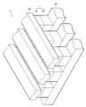
도 8은 도 1에 도시한 스위치 소자를 구비한 메모리 셀 어레이의 사시도.
도 9a는 도 8에 도시한 메모리 셀의 구성의 한 예를 도시하는 단면도.
도 9b는 도 8에 도시한 메모리 셀의 구성의 다른 예를 도시하는 단면도.
도 9c는 도 8에 도시한 메모리 셀의 구성의 다른 예를 도시하는 단면도.
도 10a는 도 8에 도시한 메모리 셀의 구성의 다른 예를 도시하는 단면도.
도 10b는 도 8에 도시한 메모리 셀의 구성의 다른 예를 도시하는 단면도.
도 10c는 도 8에 도시한 메모리 셀의 구성의 다른 예를 도시하는 단면도.
도 11a는 도 8에 도시한 메모리 셀의 기록 및 소거에서의 IV 특성을 도시하는 도면.
도 11b는 도 8에 도시한 메모리 셀(기억 소자)에서의 IV 특성을 도시하는 도면.
도 11c는 도 8에 도시한 메모리 셀에서의 IV 특성을 도시하는 도면.
도 11d는 도 8에 도시한 메모리 셀에서의 IV 특성을 도시하는 도면.
도 12는 본 개시된 실험 1에서의 IV 특성도.
도 13a는 본 개시된 실험 2(샘플 3)에서의 IV 특성도.
도 13b는 마찬가지로 실험 2(샘플 4)에서의 IV 특성도.
도 13c는 마찬가지로 실험 2(샘플 5)에서의 IV 특성도.
도 14는 샘플 3 내지 5의 IV 곡선을 종합한 특성도.
도 15는 본 개시된 실험 3에서의 IV 특성도.
도 16a는 실험 3에서의 최대 전류와 리크 전류와의 관계를 도시하는 특성도.
도 16b는 실험 3에서의 최대 전류와 스위칭 임계치 전압과의 관계를 도시하는 특성도.BRIEF DESCRIPTION OF THE DRAWINGS Fig. 1 is a cross-sectional view showing an example of the configuration of a switch element according to one embodiment of the present disclosure; Fig.
2 is a cross-sectional view of a switch element as a comparative example disclosed herein.
3 is a diagram showing IV characteristics of the switch element shown in Fig.
Fig. 4A is a schematic cross-sectional view of the switch element in each region of the IV curve shown in Fig. 3; Fig.
FIG. 4B is a schematic cross-sectional view of the switch element in each region of the IV curve shown in FIG. 3 similarly. FIG.
FIG. 4C is a schematic cross-sectional view of the switch element in each region of the IV curve shown in FIG. 3 similarly. FIG.
4D is a schematic cross-sectional view of the switch element in each region of the IV curve shown in Fig.
Fig. 4E is a schematic cross-sectional view of the switch element in each region of the IV curve shown in Fig. 3 similarly. Fig.
5 is a diagram showing IV characteristics under the conditions of the respective forming conditions (A) to (D).
6A is a schematic cross-sectional view of a switching element under a forming condition (A).
6B is a schematic cross-sectional view of the switching element under the forming condition (B).
Fig. 6C is a schematic cross-sectional view of the switching element under the forming condition (C). Fig.
Fig. 6D is a schematic cross-sectional view of the switching element in the forming condition (D). Fig.
7A is a cross-sectional view showing another example of the configuration of a switch element according to the presently disclosed embodiment;
Fig. 7B is a cross-sectional view showing another example of the configuration of the switch element according to the presently disclosed embodiment; Fig.
8 is a perspective view of a memory cell array having the switch elements shown in Fig.
FIG. 9A is a cross-sectional view showing an example of the configuration of the memory cell shown in FIG. 8; FIG.
FIG. 9B is a cross-sectional view showing another example of the configuration of the memory cell shown in FIG. 8; FIG.
FIG. 9C is a cross-sectional view showing another example of the configuration of the memory cell shown in FIG. 8; FIG.
10A is a cross-sectional view showing another example of the configuration of the memory cell shown in FIG.
10B is a cross-sectional view showing another example of the configuration of the memory cell shown in FIG.
Fig. 10C is a cross-sectional view showing another example of the configuration of the memory cell shown in Fig. 8;
11A is a diagram showing IV characteristics in the write and erase of the memory cell shown in Fig.
FIG. 11B is a diagram showing IV characteristics in the memory cell (memory element) shown in FIG. 8; FIG.
11C is a diagram showing IV characteristics in the memory cell shown in FIG. 8; FIG.
FIG. 11D is a diagram showing IV characteristics in the memory cell shown in FIG. 8; FIG.
Figure 12 is an IV characteristic diagram in
13A is an IV characteristic diagram in Experiment 2 (Sample 3) of the present disclosure.
13B is an IV characteristic diagram similarly in Experiment 2 (Sample 4).
13C is an IV characteristic diagram similarly in Experiment 2 (Sample 5).
Fig. 14 is a characteristic chart of the IV curves of
15 is an IV characteristic diagram in
16A is a characteristic diagram showing the relationship between the maximum current and the leak current in
16B is a characteristic diagram showing the relationship between the maximum current and the switching threshold voltage in
이하, 본 개시된 실시의 형태에 관해, 이하의 차례로 도면을 참조하면서 설명한다.Hereinafter, the presently disclosed embodiments will be described with reference to the drawings in the following order.
1. 실시의 형태(스위치층을 OTS층과 고저항층과의 적층 구조로 한 예)1. Embodiment (Example in which the switch layer is a laminated structure of an OTS layer and a high-resistance layer)
1-1. 스위치 소자1-1. Switch element
1-2. 기억 장치1-2. store
2. 실시례2. Examples
[1.실시의 형태][Embodiment Mode]
[1-1. 스위치 소자][1-1. Switch element]
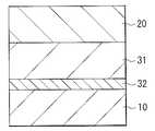
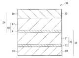
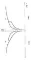
도 1은, 본 개시된 한 실시의 형태에 관한 스위치 소자(1A)의 단면 구성을 도시한 것이다. 이 스위치 소자(1A)는, 예를 들면 도 8에 도시한, 이른바 크로스 포인트 어레이 구조를 갖는 메모리 셀 어레이(2)에서 복수 마련된 중의 임의의 기억 소자(기억 소자(3Y) ; 도 8)를 선택적으로 동작시키기 위한 것이다. 스위치 소자(1A)(스위치 소자(3X) ; 도 8)는, 기억 소자(3Y)(구체적으로는 기억층(40))에 직렬로 접속되어 있고, 하부 전극(10)(제1 전극), 스위치층(30) 및 상부 전극(20)(제2 전극)를 이 순서로 갖는 것이다.Fig. 1 shows a cross-sectional configuration of a
하부 전극(10)는, 반도체 프로세스에 사용되는 배선 재료, 예를 들면, 텅스텐(W), 질화텅스텐(WN), 질화티탄(TiN), 구리(Cu), 알루미늄(Al), 몰리브덴(Mo), 탄탈(Ta), 질화탄탈(TaN) 및 실리사이드 등에 의해 구성되어 있다. 하부 전극(10)이 Cu 등의 전계(電界)에서 이온 전도(傳導)가 생길 가능성이 있는 재료에 의해 구성되어 있는 경우에는 Cu 등으로 이루어지는 하부 전극(10)의 표면을, W, WN, 질화티탄(TiN), TaN 등의 이온 전도나 열(熱)확산하기 어려운 재료로 피복하도록 하여도 좋다.The
스위치층(30)은, 예를 들면 하부 전극(10)측부터 차례로 고저항층(32)(제2층) 및 OTS층(31)(제1층)이 적층된 구성을 갖는다.The
OTS층(31)은, 적어도 주기율표 제16족의 원소, 구체적으로는, 산소(O). 유황(S), 셀렌(Se) 및 텔루르(Te) 등의 칼코겐 원소를 포함하고, 상부 전극(20)에 접하여 마련되어 있다. OTS층(31)은, 상기 칼코겐 원소 외에, 예를 들면 게르마늄(Ge), 안티몬(Sb), 규소(Si), 비소(As) 등을 포함하고 있는 것이 바람직하다. 구체적으로는, 예를 들면 GeTe, GeSbTe, SiAsTe, GeSe, GeSbSe, SiAsSe, GeS, GeSbS 또는 SiAsS 등의 칼코게나이드(chalcogenide)에 의해 구성되고, 또는 이들에 산소(O)나 질소(N)가 첨가되어 있다.The
OTS층(31)은, 상기 원소 이외의 첨가 원소로서, 예를 들면 Al, 마그네슘(Mg), 붕소(B), 이트륨(Y) 및 희토류 원소 등의 금속 원소를 포함하고 있어도 좋다. 또한, OTS층(31)은, 본 개시된 효과를 손상시키지 않는 범위에서 이들 이외의 원소를 포함하고 있어도 상관없다.The
본 실시의 형태에서의 고저항층(32)은, OTS층(31)에 접하여 마련되어 있고, 상세는 후술하지만, 층 내에 전도 패스를 가지며, 이 전도 패스에 의해 스위치 소자(1A)의 동작 면적을 제어하는 것이다. 고저항층(32)은, 예를 들면 금속 원소 또는 비금속 원소의 산화물이나 질화물 또는 이들의 혼합물 등에 의해 구성되어 있다. 고저항층(32)에는, 예를 들면 Al, 갈륨(Ga), Mg, Si, 하프늄(Hf) 및 희토류 원소 등의 산화물이나 질화물 또는 산질화물을 사용할 수 있다. 이에 의해, 초회(初回)의 기록 동작시, 즉 포밍(forming)시에 고저항층(32)의 층 내에 결함이 생성되고, 수㎚ 정도의 크기의 전도 패스(P)(예를 들면, 도 4b 참조)가 형성된다.The
또한, 고저항층(32) 내의 원소는 반드시 전부가 산화물의 상태가 아니라도 좋고, 일부가 산화되어 있는 상태라도 좋다. 또한, 고저항층(32)은 O 대신에 N을 포함하고 있어도 좋다. 고저항층(32) 중의 N은 O와 같은 작용을 한다. 고저항층(32)의 저항치는, OTS층(31)보다도 절연성이 높은 것이 바람직하다. 막두께는 특히 한정되지 않지만, 스위치층(30)의 두께를 작게 하고, 또한, 비선택(오프)시의 리크 전류를 가능한 한 작게 억제하기 위해, 예를 들면 2㎚ 이상 30㎚ 이하인 것이 바람직하다.The elements in the high-
상부 전극(20)은, 하부 전극(10)과 마찬가지로 공지의 반도체 배선 재료를 사용할 수 있지만, 포스트 어닐을 경유하여도 OTS층(31)과 반응하지 않는 안정한 재료가 바람직하다.A known semiconductor wiring material can be used for the
본 실시의 형태의 스위치 소자(1A)는, 스위칭 임계치 전압 이상의 전압의 인가에 의해 저저항화하는데, 인가 전압을 스위칭 임계치 전압보다 내리면 고저항 상태로 되돌아오는 것이다. 즉, 스위치 소자(1A)는, 도시하지 않은 전원 회로(펄스 인가 수단)로부터 하부 전극(10) 및 상부 전극(20)를 통하여 전압 펄스 또는 전류 펄스의 인가에 의해, 스위치층(30)(특히 OTS층(31))의 상(相) 변화(비정질상(어모퍼스상(相))와 결정상 사이의 변화)가 생기지 않는 것이다. 또한, 스위치 소자(1A)는 전압 인가에 의한 이온의 이동에 의해 형성되는 전도 패스가 인가 전압 소거 후에도 유지되는 등의 메모리 동작을 하지 않는 것이다. 이하, 일반적인 스위치 소자(100)(도 2)와 비교하여, 그 동작 방법 및 동작의 구조에 관해 설명한다.The
전술한 바와 같이, 메모리(메모리 셀 어레이)의 대용량화는 도 8에 도시한 바와 같은, 교차하는 배선 사이의 크로스 포인트 부근에 메모리 소자와 스위치 소자가 적층된 메모리 셀이 배치된 크로스 포인트 어레이형을 취함으로써 실현할 수 있다. 이 크로스 포인트형의 메모리 셀 어레이는, 메모리 소자로서 저항 변화형의 메모리 소자(예를 들면, 후술하는 기억 소자(3Y))를 이용할 수 있다. 저항 변화형의 메모리 소자는 여러가지의 재료에 의해 형성되지만, 일반적으로 기록하고 임계치 전압의 큰 메모리 소자일수록 높은 기록 유지 신뢰성을 갖는다. 또한, 메모리 소자의 기록 임계치 전압은 소자 사이에서의 편차를 갖는다. 이 때문에, 대규모 메모리 셀 어레이에서는 기록 임계치 전압에 여분으로 마진을 취할 필요가 있다. 예를 들면, 기록 임계치 전압이 1V의 메모리 소자라도, 스위치 소자의 스위칭 임계치 전압은 그 이상의 크기를 갖는 것이 바람직하고, 예를 들면 메모리 셀 어레이로의 기록 임계치 전압의 편차가 ±0.3V인 경우에는, 1.3V 이상인 것이 바람직하다. 따라서, 기록 임계치 전압이 높게(예를 들면, 1.5V 이상) 유지 신뢰성이 높은 메모리 소자를 기록 동작의 불량 없게 구동시키는 데는, 스위치 소자에는 더욱 높은 스위칭 임계치 전압이 요구된다.As described above, in order to increase the capacity of the memory (memory cell array), a cross-point array type in which memory elements in which memory elements and switch elements are stacked is arranged near a cross point between intersecting wires . In this cross-point type memory cell array, a resistance change type memory element (for example, a
스위치 소자(100)는, 도 2에 도시한 바와 같이 상부 전극(120)과 하부 전극(110)과의 사이에 칼코게나이드로 이루어지는 스위치층(130)이 마련된 일반적인 스위치 소자이다.The
도 8에 도시한 바와 같은 크로스 포인트 어레이형의 메모리 셀 어레이(2)의 기억 소자로서 예를 들면, 저항 변화형의 기억 소자(기억 소자(3Y))를 이용하는 경우에는, 스위치 소자에는, 온 상태에서의 충분한 전류 밀도와, 오프 상태에서의 리크 전류의 발생을 억제할 것이 요구된다. 이에 대해, 스위치 소자(100)에서는, 스위칭 임계치 전압은 그다지 크지 않고, 예를 들면 1 내지 1.5V 정도의 것이 대부분이고, 기억 소자(3Y)와 같은 메모리 소자를 구동시키기 위해서는, 그 스위칭 임계치 전압의 값은 불충분하였다. 이 때문에, 스위치 소자(100)와 기억 소자(3Y)를 조합시킨 경우에는, 스위치 소자가 메모리 소자보다도 우선 스위치하여 버려, 선택(온) 상태 및 반선택(오프) 상태의 선택비(온-오프비)를 충분 확보할 수가 없다는 문제가 있다.When a storage element of the resistance variable memory element (
이것은, 스위치 소자(100)를 구성한 하부 전극(110) 및 상부 전극(120)의 전극면적이 그대로 동작 영역이 되기 때문이고, 비선택(오프) 상태의 리크 전류가 큰 것이 많아 오작동(오기록이나 오소거)를 일으키기 쉬워진다. 또한, 리크 전류가 작다는 점에서 우수한 것도 있지만, 스위칭 임계치 전압이 1V 이하로 작았다. 이 때문에, 이 스위치 소자(100A)가 상기 조건을 충족시키기 위해서는, 스위치층(130)의 막두께를 크게(예를 들면, 180㎚ 정도)할 필요가 있고, 그 경우에는 미세화할 수 없게 된다는 문제가 있다.This is because the electrode areas of the
또한, 리크 전류의 문제는, 메모리 셀 어레이의 대형화와 비례하여 심각해지기 때문에, 보다 큰 온-오프비가 요구된다. 따라서, 기록 임계치 전압의 큰 메모리 소자와 상기 스위치 소자(100)를 조합시킨 메모리 셀에서는, 기록-판독 마진이 작아 대용량 메모리 셀 어레이를 정상적으로 동작시키는 것은 곤란하였다.Further, since the problem of the leakage current becomes serious in proportion to the enlargement of the memory cell array, a larger on-off ratio is required. Therefore, in the memory cell in which the
이에 대해, 본 실시의 형태의 스위치 소자(1A)에서는, 스위치층(30)를 칼코게나이드에 의해 구성되는 OTS층(31)(상기 스위치층(130)에 상당)과 고저항층(32)과의 적층 구조로 한다. 이 스위치 소자(1A)는, 초회의 온 동작시에 고저항층(32) 내에 미세한 전도 패스(P)가 형성된다. 고저항층(32) 내에 형성된 전도 패스(P)는, 그 형성 영역(예를 들면, 평면 방향으로 수㎚ 정도)가 스위치 소자(1A)의 동작 영역이 된다.On the other hand, in the
구체적으로는, 일단 고저항층(32)에 전도 패스(P)가 형성되면, 스위치 소자(1A)에 인가된 전압의 대부분이 OTS층(31)에 인가되게 되고, OTS층(31)에 전계가 인가된다(예를 들면, 도 3 및 도 4 참조). OTS층(31)은, 전계의 강함이 일정치 이상이 되면 칼코겐 원소의 전자 상태에 기인한 전리(電離) 충돌에 의한 전하 담체(캐리어)가 증대하여 급격하게 전류가 증대하여, 저저항화한다. 즉, 스위치 소자(1A)는, 이른바 오보닉 임계치 스위치 현상이 생기고 온 상태가 된다. 또한, 스위치 소자(1A)에의 인가 전압을 정지하면, OTS층(31)은, 전리 충돌에 의해 생긴 캐리어가 재결합하여 소멸하여 재차 고저항 상태로 되돌아온다. 이에 의해, 스위치 소자(1A)는 큰 온-오프비를 얻을 수 있다.Specifically, once the conductive path P is formed in the high-
이상의 것으로부터, 상기 스위치 소자(100A)와 같이 스위치층(130)(여기서는 OTS층(31))를 후막화하는 일 없이, 온 상태에서의 충분한 전류 밀도를 확보할 수 있고, 또한 오프 상태에서의 비선택 소자 및 반선택 소자에의 리크 전류를 억제하는 것이 가능해진다. 즉, 온-오프비를 증대시킬 수 있다.As described above, it is possible to secure a sufficient current density in the ON state without making the switch layer 130 (here, the OTS layer 31) thick, like the switch element 100A, It is possible to suppress the leakage current to the non-selection element and the half-selection element. That is, the on-off ratio can be increased.
또한, 스위치 소자(1A)의 임계치 전압은, 고저항층(32)의 막두께나 재료를 선택함에 의해 조정하는 것이 가능하기 때문에, 기억 소자(3Y)와 같이 높은 인가 전압이 필요한 기억 소자를 구비한 기억 장치로의 동작이 가능해진다.Since the threshold voltage of the
스위치 소자(1A)는 이하의 방법에 의해 조정된다.The
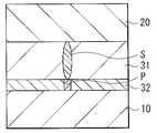
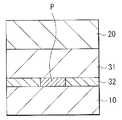
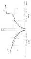
도 3은, 스위치 소자(1A)에서의 인가 전압과 전극에 흐르는 전류치와의 관계(IV 특성)를 도시한 것이다. 도 4a 내지 도 4e는, 도 3에 도시한 IV 곡선의 각 부분(A, A', A", B, B')에서의 스위치층(30) 내를 모식적으로 도시한 것이다. 우선, 포토 리소그래피나 드라이 에칭 등을 이용하여 작성된 스위치 소자(1A)는, 상술한 바와 같이, 초회의 온 동작시에 고저항층(32) 내에 전도 패스(P)가 형성되고, 스위치 소자(1A)의 동작 영역이 결정된다.3 shows the relationship (IV characteristic) between the voltage applied to the
이때의 스위치 소자(1A)의 IV 곡선은 도 3에 도시한 바와 같이 변화한다. 구체적으로는, 스위치 소자(1A)에 흐르는 전류는, 전압의 증가에 비례하여 서서히 증가(A)한 후, 소정의 전압(스위칭 임계치 전압)에서 급격하게 증대(A')하고, 그 후, 상한에 달한다(A"). 스위치 소자(1A)의 내부(특히, 스위치층(30))는, IV 곡선의 각 부분(A, A', A")에서 도 4a 내지 도 4c와 같이 변화한다고 생각된다. 예를 들면, 스위치 소자(1A)는, 도 4a에 도시한 바와 같이 인가 전압이 스위칭 임계치 전압까지는 스위치층(30)(OTS층(31) 및 고저항층(32)) 내에 변화는 보여지지 않지만, 도 4b에 도시한 바와 같이, 스위칭 임계치 전압에 달함으로써 고저항층(32)에 전도 패스(P)가 형성됨과 함께, OTS층(31) 내에 전리 충돌 영역(S)이 발생하여 저저항화한다. 이에 의해, 전류가 급격하게 증대한다. 이 후, 스위치 소자(1A)는 설정된 상한의 전류 밀도가 얻어질 때까지 전압이 인가되는데, 이때 전도 패스(P) 및 전리 충돌 영역(S)의 크기는 도 4c에 도시한 바와 같이 커져 간다고 생각된다. 이와 같이 하여, 스위치 소자(1A)는 포밍된다.The IV curve of the
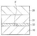
이 후, 인가 전압을 감소시키면 스위치 소자(1A)의 IV 특성은 도 3에 도시한 B-B'의 경로를 통과하여 변화한다. 즉, 스위치 소자(1A)의 스위치층(30)은, 상한 전류에 달한 때에 형성된 전도 패스(P)(도 4c)를 유지한 채로, 도 4d에 도시한 바와 같이 OTS층(31) 내에 생긴 전리 충돌 영역(S)가 서서히 축소된다. 이에 수반하여, 스위치 소자(1A)에 흐르는 전류는 저하되어 가고(B), 어느 임계치 전압에 달한 곳에서 캐리어의 재결합이 일어나 도 4e에 도시한 바와 같이 전리 충돌 영역(S)이 소멸하여 OTS층(31)의 저항치가 급격하게 증대한다. 이에 의해, 도 3에 도시한 바와 같이 전류가 급격하게 감소하고, 그 후, 인가 전압의 감소와 함께 전류도 서서히 감소한다(B').Thereafter, when the applied voltage is decreased, the IV characteristic of the
또한, 2회째 이후의 온 동작시의 스위치 소자(1A)에서의 IV 특성은, B-B'의 경로에 근사한 변화를 나타내게 된다.Further, the IV characteristic in the
도 5는, 각 포밍 조건(조건 A 내지 D)에서의 2회째 이후의 온 동작시의 IV 특성을 도시한 것이고, 도 6a 내지 도 6d는 각 조건시에 있어서의 스위치 소자(1A)의 단면 구성을 모식적으로 도시한 것이다. 또한, 포밍 조건은, 조건 A부터 조건 D에 걸쳐서 포밍 전류를 서서히 작게 하고 있다. 도 6a 내지 도 6d로부터 알 수 있는 바와 같이, 초회의 온 전류를 보다 크게 하면, 고저항층(32) 내에 형성된 전도 패스(P)의 형성 영역은 커져서, 보다 큰 온 전류를 흘릴 수 있도록 된다. 즉, 초회의 온 동작시(포밍시)에서의 전류치 또는 인가 전압의 최대치를 변화시킴에 의해 스위치 소자(1A)의 특성을 제어할 수 있다. 단, 전도 패스가 너무 커지면 오프(OFF)시의 리크 전류가 커질 우려가 있기 때문에 조정이 필요해진다.Fig. 5 shows the IV characteristics at the second ON-time operation in each of the forming conditions (conditions A to D), and Figs. 6A to 6D show the IV characteristic at the time of the ON operation at the second and subsequent times under the respective forming conditions As shown in FIG. In addition, the forming condition gradually reduces the forming current from the condition A to the condition D. As can be seen from Figs. 6A to 6D, when the initial ON current is made larger, the region in which the conductive path P formed in the high-
이와 같이, 상기 동작을 행함에 의해, 소망하는 특성, 즉, 선택 상태(온 상태)에서는 저저항 상태로, 비선택 상태(오프 상태)에서는 고저항 상태로 변화하는 스위치 소자(1A)를 얻을 수 있다. 동시에, 초회 기록에 의한 포밍 동작에 의해 2회째 이후의 동작 특성을 제어할 수 있다.As described above, by performing the above operation, the
이상과 같이, 본 실시의 형태에서는, 스위치층(30)를 구성하는 OTS층(31)에 고저항층(32)을 적층하도록 하였기 때문에, 스위치층(30)의 동작 영역이 제한되고, 비선택 또는 반선택시(오프 상태)에서의 리크 전류의 발생을 저감하는 것이 가능해진다. 또한, 스위칭 임계치 전압 및 온-오프비가 커진다. 따라서, 고밀도면서 대용량차의 기억 장치를 제공하는 것이 가능해진다.As described above, in the present embodiment, since the
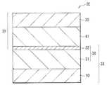
또한, 본 실시의 형태의 스위치 소자(1A)는 OTS층(31)과 고저항층(32)이 접하여 있으면 좋고, 도 1에 도시한 적층 구조로 한정되지 않는다. 예를 들면 도 7a에 도시한 바와 같이, 상부 전극(20)측에 고저항층(32)을 형성하여도 상관없다. 또한, 도 7b에 도시한 바와 같이, OTS층(31)를 끼우도록, 즉, 상부 전극(20)측 및 하부 전극(10)측의 양쪽에 고저항층(32A, 32B)를 형성하여도 상관없다. 또한, OTS층(31) 및 고저항층(32)을 복수조 적층한 다층 구조로 하여도 좋다.The
[1-2. 기억 장치][1-2. store]
기억 장치(메모리)는, 후술하는 기억 소자(3Y)를 다수, 예를 들면 열형상(列狀)이나 매트릭스형상으로 배열함에 의해 구성할 수 있다. 이때, 본 개시된 스위치 소자(1A)는, 스위치 소자(3X)로서, 기억 소자(3Y)와 직렬로 접속되어 있고, 이에 의해 메모리 셀(3)을 구성하고 있다. 메모리 셀(3)은, 배선을 통하여 센스 앰프, 어드레스 디코더 및 기록·소거·판독 회로 등에 접속된다.The storage device (memory) can be configured by arranging a plurality of
도 8은, 교차하는 배선 사이의 교점(크로스 포인트)에 메모리 셀(3)을 배치한, 이른바 크로스 포인트 어레이형의 기억 장치(메모리 셀 어레이(2))의 한 예를 도시한 것이다. 이 메모리 셀 어레이(2)에서는, 각 메모리 셀(3)에 대해, 그 하부 전극(10)측에 접속된 배선(예를 들면 비트선 ; BL(행 라인))과, 그 상부 전극(20)측에 접속된 배선(예를 들면 워드선 ; WL(세로 라인))을 교차하도록 마련하고, 예를 들면 이들 배선의 교차점 부근에 각 메모리 셀(3)이 배치되어 있다. 이와 같이, 크로스 포인트 어레이 구조를 이용함에 의해, 단위셀당의 플로어 면적을 작게 하는 것이 가능하고, 대용량화를 실현하는 것이 가능해진다.Fig. 8 shows an example of a so-called cross-point array type storage device (memory cell array 2) in which the
메모리 셀(3)를 구성하는 기억 소자(3Y)는, 예를 들면, 하부 전극, 기억층(40) 및 상부 전극을 이 순서로 갖는 것이다. 기억층(40)은, 예를 들면 하부 전극측부터 저항 변화층(42) 및 이온원층(源層)(41)이 적층된 적층 구조 또는 저항 변화층(42)의 단층 구조에 의해 구성되어 있다. 또한, 여기서는 스위치층(30)과 기억층(40)과의 사이에는 중간 전극(50)이 마련되어 있고, 이 중간 전극(50)이 스위치 소자(3X)의 상부 전극과, 기억 소자(3Y)의 하부 전극을 겸하고 있다. 구체적으로는, 메모리 셀(3)은, 예를 들면 도 9a에 도시한 바와 같이, 하부 전극(10)과 상부 전극(20)과의 사이에, 스위치층(30), 중간 전극(50), 저항 변화층(42) 및 이온원층(41)이 이 순서로 적층된 구성을 갖는다.The
기억층(40)은, 상기한 바와 같이, 예를 들면 이온원층(41)과 저항 변화층(42)과의 적층 구조와 같은 구성을 갖는, 이른바 저항 변화형 기억 소자(메모리 소자)라면 좋다. 예를 들면 천이금속 산화물에서 이루어지는 저항 변화 메모리, PCM(Phase Change Memory ; 상 변화형 메모리) 또는 MRAM(Magnetoresistive Random Access Memory ; 자기 저항 변화형 메모리)를 이용하여도 상관없다.The
이온원층(41)은, 전계의 인가에 의해 저항 변화층(42) 내에 전도 패스를 형성하는 가동 원소를 포함하고 있다. 이 가동 원소는, 예를 들면 천이금속 원소(주기율표 제4족 내지 제6족) 및 칼코겐 원소이고, 이온원층(41)은 이들을 각각 1종 또는 2종 이상 포함하여 구성되어 있다. 또한, 이온원층(41)은, 산소(O)나 질소(N)나, 상기 원소 이외의 원소, 예를 들면 Al, Cu, 망간(Mn), 코발트(Co), 철(Fe), 니켈(Ni) 및 백금(Pt), Si 등을 포함하고 있어도 상관없다.The
저항 변화층(42)은, 예를 들면 금속 원소 또는 비금속 원소의 산화물 또는 질화물에 의해 구성되어 있고, 하부 전극(10)과 상부 전극(20)과의 사이에 소정의 전압을 인가한 경우에 그 저항치가 변화하는 것이다. 구체적으로는, 하부 전극(10)과 상부 전극(20)과의 사이에 전압이 인가되면, 이온원층(41)에 포함되는 천이금속 원소가 저항 변화층(42) 내로 이동하여 전도 패스가 형성되고, 저항 변화층(42)은 저저항화한다. 또는, 저항 변화층(42) 내에서 산소 결함이나 질소 결함 등의 구조 결함이 생겨서 전도 패스가 형성되고, 저항 변화층(42)은 저저항화한다. 또한, 역방향의 전압을 인가함에 의해 전도 패스는 절단, 또는 도전성이 변화한다. 이에 의해, 저항 변화층(42)은 고저항화한다.The
또한, 저항 변화층(42)에 포함되는 금속 원소 및 비금속 원소는 반드시 전부가 산화물의 상태가 아니라도 좋고, 일부가 산화되어 있는 상태라도 좋다. 또한, 저항 변화층(42)의 초기 저항치는, 예를 들면 수MΩ부터 수백GΩ 정도의 소자 저항이 실현되면 좋고, 소자의 크기나 이온원층(41)의 저항치에 의해서도 그 최적치가 변화하지만, 그 막두께는 예를 들면 1㎚ 내지 10㎚ 정도가 바람직하다.The metal element and the non-metal element contained in the resistance-
중간 전극(50)은, 예를 들면 전계의 인가에 의해 칼코게나이드를 포함하는 OTS층(31) 및 이온원층(41) 내에 이온의 용해·석출 등의 산화환원 반응 및 이온의 이동이 생기기 어려운 불활성한 재료라면 특히 묻지 않는다.The
기억 소자(3Y)는, 도시하지 않은 전원 회로(펄스 인가 수단)로부터 하부 전극(10) 및 상부 전극(20)를 통하여 전압 펄스 또는 전류 펄스를 인가하면, 기억층(40)의 전기적 특성(저항치)가 변화하는 저항 변화형의 기억 소자이고, 이에 의해 정보의 기록, 소거, 또한 판독이 행하여진다.When the voltage pulse or the current pulse is applied from the power supply circuit (pulse applying means) not shown through the
구체적으로는, 기억 소자(3Y)에서는, 초기 상태(고저항 상태)의 소자에 대해 "정방향"(예를 들면 제1 전극측을 부전위, 제2 전극측을 정전위)의 전압 또는 전류 펄스가 인가되면, 이온원층에 포함되는 금속 원소(예를 들면, 천이금속 원소)가 이온화하여 기억층 중(예를 들면, 저항 변화층 중)에 확산, 또는 산소 이온이 이동함에 의해 저항 변화층 중에 산소 결함이 생성한다. 이에 의해 기억층 내에 산화 상태가 낮은 저저항부(전도 패스)가 형성되고, 저항 변화층의 저항이 낮아진다(기록 상태). 이 저저항한 상태의 소자에 대해 "부방향"(예를 들면 제1 전극측을 정전위, 제2 전극측을 부전위)에 전압 펄스가 인가되면, 저항 변화층 중의 금속 이온이 이온원층 중으로 이동, 또는 이온원층으로부터 산소 이온이 이동하여 전도 패스 부분의 산소 결함이 감소한다. 이에 의해 금속 원소를 포함하는 전도 패스가 소멸하고, 저항 변화층의 저항이 높은 상태가 된다(초기 상태 또는 소거 상태). 또한, 기억층(40)을 저항 변화층(42)의 단층으로 구성하는 경우에는, 정방향의 전압(또는 전류 펄스)가 인가된 경우와, 저항 변화층(42)에 인가된 전계 따라서 결함이 생성되고, 부방향으로 전압 펄스가 인가되면, 결함은 저항 변화층 내의 산소 이온이나 질소 이온의 이동에 의해 수복된다.Specifically, in the
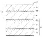
또한, 메모리 셀(3)의 스위치 소자(3X) 및 기억 소자(3Y)의 적층 구조는, 도 9a에 도시한 메모리 셀(3A)의 적층순으로 한정되는 것이 아니다. 예를 들면, 도 9b에 도시한 메모리 셀(3B)과 같이, 중간 전극(50)을 사이로 스위치층(30)을 상부 전극(20)측에, 기억층(40)를 하부 전극(10)측에 마련하도록 하여도 좋다. 또는, 도 9c에 도시한 메모리 셀(3C)와 같이, 중간 전극(50)을 사이로 OTS층(31) 및 이온원층(41)을 대향 배치시켜, 고저항층(32) 및 저항 변화층(42)을 각각 하부 전극(10)측 또는 상부 전극(20)측에 배치하도록 하여도 좋다.The stacking structure of the
또한, 메모리 셀(3)은 중간 전극(50)을 생략한 구성으로 하여도 좋다. 이 경우에는, 도 10a에 도시한 메모리 셀(3D)과 같이, 하부 전극(10)측부터 고저항층(32), OTS층(31)의 순서로 마련된 스위치층(30)과, 하부 전극(10)측부터 저항 변화층(42), 이온원층(41)의 순서로 마련된 기억층(40)을 단순하게 적층시킨 구성으로 하여도 좋다. 또한, 스위치층(30)과 이온원층(40)과의 적층 순서는 교체하여 형성하여도 상관없다. 또한, 상술한 고저항층(32)에서의 전도 패스의 생성 및 소멸은, 기억 소자(3Y)에서의 저항 변화층(42)과 마찬가지 동작이기 때문에, 고저항층(32) 및 저항 변화층(42)을 서로 공유할 수 있다. 이 때문에, 예를 들면 도 10b에 도시한 메모리 셀(3E)과 같이, 스위치층(30)의 고저항층(32)이 기억층(40)의 1저항 변화층(42)을 겸하도록, 고저항층(32)을 사이로 OTS층(31) 및 이온원층(41)이 배치된 구성으로 하여도 좋다. 또한, 예를 들면 도 10c에 도시한 메모리 셀(3F)과 같이, 저항 변화층(42)을 2층 마련하고(저항 변화층(42A, 42B)), 이온원층(41)의 하부 전극측(10) 및 상부 전극측(30)의 양쪽에 마련하여, 스위치층(30)과 적층하여 구성하여도 좋다.The
또한, 본 실시의 형태에서의 기억 장치는, 기억층(40)에, 이른바 PCM 및 MRAM의 구성을 적용한 경우도 마찬가지이다.The storage device according to the present embodiment is also applicable to the case where the configuration of so-called PCM and MRAM is applied to the
도 11a 내지 도 11d는, 본 실시의 형태의 스위치 소자(1A)(1B, 1C 또는 3X), 기억 소자(3Y) 및 이들을 조합시킨 메모리 셀(3)의 기록시(예를 들면, 순바이어스) 및 소거시(예를 들면, 역바이어스)에서의 인가 전압과 전극에 흐르는 전류치와의 관계를 도시한 것이다. 실선은 전압 인가시에 있어서의 IV 특성을, 점선은 인가 전압을 감소 방향에 소인한 때의 IV 특성을 도시하고 있다.11A to 11D are diagrams for explaining a case in which the
도 11a는, 스위치 소자(3X)의 IV 특성을 도시한 것이다. 순바이어스(여기서는, 기록 전압)을 인가하면, 스위치 소자(3X)는 상술한 바와 같이 인가 전압의 증가에 수반하여 전류가 상승하지만, 어느 임계치 전압(스위칭 임계치 전압)을 초과하면 오보닉 임계치 스위치에 의해 급격하게 전류가 증대, 또는 저항이 낮아져서 온 상태가 된다. 이 후, 인가 전압을 감소시켜 가면, 스위치 소자(3X)의 전극에 흐르는 전류치는 서서히 감소하고, 2회째 이후의 동작에서는, 인가 전압의 증가시 및 감소시 함께 근사한 저항 변화, 구체적으로는, 증가시와 동등한 전압에서 급격하게 저항이 상승하여 오프 상태가 된다(B1). 즉, 스위치 소자(3X)의 저항치는 기록 전압의 인가에 의해 저저항 상태가 되지만, 인가 전압을 임계치 이하로 내리면 고저항 상태로 되돌아오고, 전압 인가시의 저항치는 유지되지 않는다.11A shows IV characteristics of the
도 11b는, 기억 소자(3Y)의 IV 특성을 도시한 것이다. 도 11b로부터 알 수 있는 바와 같이, 기억 소자(3Y)에서는, 인가 전압의 증가에 수반하여 전류치가 상승하지만, 어느 임계치 전압에 있어서 기억층(40)의 저항 변화층(42)에서의 전도 패스 형성에 의한 기록 동작이 행해지고, 저저항 상태로 변화한다. 즉, 기억 소자(3Y)의 저항치는 기록 전압의 인가에 의해 저저항 상태가 되고, 인가 전압 정지 후도 그 저항 상태는 유지된다(B1).Fig. 11B shows IV characteristics of the
도 11c는, 메모리 셀(3)의 IV 특성을 도시한 것이다. 상기 기억 소자(3Y)와 스위치 소자(3X)를 조합시킨 메모리 셀(3)의 기록 전압의 인가 시작 및 정지에서의 전류치의 스위칭 거동은, 기억 소자(3Y)(A1) 및 스위치 소자(3X)(B1)를 합친 것으로 된다(C1). 예를 들면, V/2 바이어스 방식의 크로스 포인트 어레이의 경우에는, 메모리 셀(3)의 C1의 IV 곡선형상으로 급격하게 저항 변화한 임계치보다도 큰 전압을 판독 전압(Vread)을 설정하고, Vread/2는 저항 변화의 임계치보다도 작은 전압이 되도록 설정한다. 이에 의해, 바이어스(온)와 Vread/2 바이어스(오프)의 전류비로 정의되는 선택비를 크게 취하는 것이 가능해진다. 또한, 상기한 바와 같이, 메모리 셀(3)의 IV 곡선(C1)은 스위치 소자(3X)의 IV 곡선(B1)과 기억 소자(3Y)의 IV 곡선의 합성이기 때문에, 스위치 소자(3X)의 오보닉 임계치 스위치의 임계치 전후의 저항 변화(또는 전류 변화)가 클수록 선택비를 크게 취할 수 있다. 이에 의해, 본 실시의 형태에서의 스위치 소자(3X)에서는 큰 온-오프비를 얻는 것이 선택비의 증대가 되어 바람직하다고 말할 수 있다. 또한, 선택비가 크면 클수록 판독 마진이 커지기 때문에, 오판독하는 일 없이 크로스 포인트 어레이 사이즈를 크게 하는 것이 가능해지고, 메모리 셀 어레이의 더한층의 대용량화가 가능하게 된다.Fig. 11C shows the IV characteristics of the
이것은, 판독 동작뿐만 아니라, 기록 동작에 대해서도 마찬가지이다. 도 11d는, 도 11c와 마찬가지로 메모리 셀(3)의 IV 특성을 도시한 것이다. 상술한 바와 같이, 크로스 포인트 어레이에서는, 대상의 메모리 셀과 같은 비트선(BL) 또는 워드선(WL)에 다수의 비트가 접속되어 있다. 이 때문에, 도 11d에 도시한 바와 같이, Vwrite/2와 IV 곡선(C1)의 점선의 Set 상태의 IV 루프의 교점에서 나타난다, Vwrite/2로 바이어스된 비선택시의 리크 전류가 크면 비선택의 메모리 셀에서 오기록이 생길 우려가 있다. 따라서, 기록 동작에서는, 기억 소자(3Y)를 기록할 때에 필요한 전류를 얻을 수 있는 전압으로 기록 전압(Vwrite)을 설정한 다음, Vwrite/2로 바이어스된 비선택의 메모리 셀이 오기록이 생기지 않을 정도의 리크 전류로 억제할 필요가 있다. Vwrite/2로 바이어스된 비선택시의 리크 전류가 작으면 작을수록 대규모 크로스 포인트 어레이를 오기록 없이 동작시킬 수 있다. 따라서, 기록 동작시도 스위치 소자(3X)의 선택비를 크게 하는 것이, 메모리 셀 어레이의 대용량화에 연결된다.This applies not only to the read operation but also to the write operation. 11D shows IV characteristics of the
한편, 반대 바이어스(여기서는 소거 전압)를 인가하면, 스위치 소자(3X)의 소거 전압 인가시에 있어서의 전류치의 변화는, 기록 전압을 인가한 때와 같은 거동을 나타낸다(B2). 이에 대해, 기억 소자(3Y)의 소거 전압 인가시에 있어서의 전류치의 변화는, 소거 임계치 전압 이상의 전압 인가에 의해, 저저항 상태로부터 고저항 상태로 변화한다(A2). 도 11에 도시한 바와 같이, A2 및 B2의 IV 특성을 합성하면 소거 바이어스로의 메모리 셀의 IV 특성(C2)를 얻을 수 있다. V/2 바이어스 방식의 크로스 포인트 어레이에서는, 통상의 판독 바이어스를 기록측에 설정하기 때문에, Vreset/2 바이어스에서의 디스터브 전류(disturb current)가 문제가 되지만, 이에 대해서도, 정바이어스의 경우와 마찬가지로, 스위치 소자(3X)의 온-오프비, 즉 선택비가 크고, 오프(OFF)시의 리크 전류가 작을수록 크로스 포인트 어레이의 대규모화에 유리하게 된다.On the other hand, when the opposite bias (here, erase voltage) is applied, the change in the current value when the erase voltage is applied to the
본 실시의 형태의 기억 장치에서는, 저항 변화형의 기억 소자(3Y)를 이용한 메모리 장치 이외에 각종의 메모리 장치에 적용할 수 있다. 예를 들면, 한번만 기록이 가능한 PROM, 전기적으로 소거가 가능한 EEPROM, 또는, 고속으로 기록·소거·재생이 가능한, 이른바 RAM 등, 어느 메모리 형태라도 적용하는 것이 가능하다.The memory device of the present embodiment can be applied to various memory devices other than the memory device using the resistance change
또한, 본 실시의 형태의 기억 장치에서는, 메모리 셀(3)을 평면(2차원)으로 복수 배치한 구성으로 하였지만, 예를 들면 메모리 셀(3)를 다수 적층하여 3차원화하여도 좋다. 이에 의해, 보다 고밀도면서 대용량의 기억 장치(메모리)를 제공할 수 있다.Further, in the memory device of the present embodiment, a plurality of
[2. 실시례][2. Examples]
이하, 본 개시된 구체적인 실시례에 관해 설명한다.Hereinafter, a specific embodiment of the present invention will be described.
[실험 1][Experiment 1]
우선, TiN으로 이루어지는 하부 전극(10)을 역스퍼터에 의해 클리닝한 후, TiN상에 SiO2막을 2㎚의 막두께로 형성하여 고저항층(32)으로 한다. 다음에, OTS층(31)으로서 GeTe막을 40㎚의 막두께로 형성한 후, W를 30㎚의 막두께로 형성하여 상부 전극(20)으로 하였다. 계속해서, 포토 리소그래피나 드라이 에칭 등의 공지의 기술을 이용하여 소자 사이즈가 100㎚φ가 되도록 미세 가공을 행하여, 스위치 소자(1A)(샘플 1)를 제작하였다. 또한, 비교례로서, 고저항층(32)을 형성하지 않은 스위치 소자(100A)(샘플 2)를 제작하였다. 이들 샘플 1 및 샘플 2의 인가 전압과 각 전극에 흐르는 전류치와의 관계를 측정하고, 그 IV 특성을 도 12에 도시하였다.First, the
도 12로부터 알 수 있는 바와 같이, 본 실시의 형태인 샘플 1에서는, 샘플 2와 비교하여 임계치 전압이 증대하였다. 또한, 온-오프비도 샘플 1보다도 커졌다. 즉, 스위치 소자(1A)는 임계치 전압의 증가와 저항 변화비의 증대가 동시에 실현하고 있음을 알 수 있다.As can be seen from Fig. 12, in the
이것은, OTS층(31)에 접하도록 고저항층(32)을 형성함에 의한다고 생각된다. 구체적으로는, 어느 전압 이상의 전압을 인가함에 의해 고저항층(32)은 층 중에 전도 패스가 형성되고, 이에 의해 저저항화함과 함께, 스위치층(30)의 동작 영역이 규제된다. 그 후, 인가 전압이 임계치 전압에 달함에 의해, 스위치 소자(1A)에 큰 전류가 흐른다.It is considered that this is due to the formation of the
[실험 2][Experiment 2]
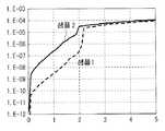
다음에, OTS층(31)으로서 40㎚의 두께의 MgTeBO막을, 고저항층(32)으로서 2㎚의 두께의 SiO2막을 형성하고, 스위치 소자(1A)(샘플 3)를 제작하였다. 마찬가지로, OTS층(31)으로서 40㎚의 두께의 MgTeBO막을, 고저항층(32)으로서 5㎚의 두께의 SiN막을 형성한 스위치 소자(1A)(샘플 4)를 제작하였다. 이 밖에, 비교를 위해 전극 사이에 MgTeBO막으로 이루어지는 OTS층(31)만을 형성(고저항층(32)은 미형성)한 스위치 소자(100)(샘플 5)를 제작하였다. 이들 샘플 3 내지 5의 IV 특성을 도 13a(샘플 3), 도 13b(샘플 4), 도 13c(샘플 5)에 도시하였다.Next, an MgTeBO film having a thickness of 40 nm was formed as the
도 13a 내지 도 13c로부터 알 수 있는 바와 같이, 스위치 소자(1A)(샘플 3, 4) 및 스위치 소자(100)(샘플 5)는, 고저항층(32)의 유무에 의하지 않고, 어느 임계치 전압을 경계로에 급격의 저항이 저하되어 전류가 증대한 오보닉 임계치 스위치가 보여진다. 도 14는, 도 13a 내지 도 13c에 도시한 샘플 3 내지 5의 정 바이어스의 인가 전압 증가 방향의 IV 곡선을 종합한 것이다. 샘플 3, 4를 고저항층(32)을 마련하지 않은 샘플 5와 비교하면, 샘플 3 및 샘플 4는 함께 오프 상태(전압 0)에서의 리크 전류가 저감(거의 0)되고, 또한 임계치 전압이 증대하고 있다. 즉, 본 개시된 스위치 소자(1A)는 기록 임계치 전압이 높은 기억 소자(예를 들면, 기억 소자(3Y))에 대항 가능한 양호한 특성을 가짐을 알 수 있다. 또한, 샘플 3과 샘플 4를 비교한 경우에는, SiO2를 이용한 샘플 3보다도 SiN을 이용한 샘플 4의 쪽이, 임계치 전압이 높고 리크 전류가 작았다. 이것은, SiO2 및 SiN의 막두께나 성막 조건에 의해 적절히 제어할 수 있다.As can be seen from Figs. 13A to 13C, the
이와 같이, 고저항층(32)에 이용하는 재료로서는 산화물이라도 질화물이라도 상관없다. 또한, 본 실시례에서는 나타내고 있지 않지만, 고저항층(32)의 재료는 Si의 산화물 및 질화물 이외에도, Al, Ga, Mg, Hf, 희토류 원소 등의 산화물이나 질화물 또는 산질화물을 사용하여도 같은 효과를 얻을 수 있다.As such, the material used for the
[실험 3][Experiment 3]
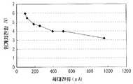
다음에, 샘플 3을 이용하여 최대 인가 전압을 6V 일정하게 하고, 스위치 소자(1A)에 직렬로 접속되어 있는 저항치를 변화(5kΩ, 12.5kΩ, 50kΩ)시킴에 의해 최대 전류치를 변화시켰다. 도 15는 각 저항치에서의 정바이어스의 IV 곡선을 도시한 것이다. 스위치 소자(1A)에 흐르는 최대 전류치가 변화함에 의해, 리크 전류와 임계치 전압이 변화함을 알았다. 다음에, 이들의 측정에서 구한 샘플 3에 흘리는 최대 전류와 리크 전류와의 관계 및 최대 전류와 임계치 전압과의 관계를 도 16a, 도 16b에 도시하였다. 또한, 리크 전류의 정의(定義)는 정바이어스 0.5V의 전류로 하였다.Next, the maximum current value was changed by changing the maximum applied voltage to
도 16a 및 도 16b로부터, 본 실시의 형태의 스위치 소자(1A)에서는, 어느 정도의 최대 전류를 흘리는지에 의해 오프 상태의 리크 전류와 임계치 전압을 제어할 수 있음을 알 수 있었다. 즉, 초회 전압 인가시에 소정의 조건을 이용한 포밍을 행함으로써 스위치 소자의 특성을 제어 가능해진다.16A and 16B, it can be seen that, in the
이상의 것으로부터, 본 실시의 형태의 스위치 소자(1A)는, 칼코게나이드에 의해 구성되는 OTS층(31)에 일정한 전압으로 저항 변화하는 고저항층(32)을 적층함에 의해 저항 변화비를 저하시키는 일 없이, 임계치 전압을 증대시키는 것이 가능함을 알았다.As described above, in the
또한, 상기 실시의 형태 및 실시례에 기재된 효과는 반드시 한정되는 것이 아니고, 본 개시 중에 기재된 어느 하나의 효과라도 좋다.The effects described in the above embodiments and examples are not necessarily limited, and any of the effects described in the present disclosure may be used.
또한, 본 기술은 이하와 같은 구성도 취할 수 있다.The present technology can also take the following configuration.
(1) 제1 전극,(1) a first electrode,
상기 제1 전극에 대향 배치된 제2 전극 및A second electrode disposed opposite to the first electrode,
상기 제1 전극과 상기 제2전극과의 사이에 마련된 스위치층을 포함하고,And a switch layer provided between the first electrode and the second electrode,
상기 스위치층은,Wherein the switch layer comprises:
칼코겐 원소를 포함하는 제1층과,A first layer comprising a chalcogen element,
고저항 재료를 포함하는 제2층을 포함하는 스위치 소자.And a second layer comprising a high-resistance material.
(2) 상기 제2층은 상기 제1층의 적어도 한쪽의 면에 접하여 마련되어 있는 상기 (1)에 기재된 스위치 소자.(2) The switch element according to (1), wherein the second layer is provided in contact with at least one surface of the first layer.
(3) 상기 제1층은 산소(O), 유황(S), 셀렌(Se) 및 텔루르(Te) 중 적어도 하나를 포함하고 있는 상기 (1) 또는 (2)에 기재된 스위치 소자.(3) The switch element according to (1) or (2), wherein the first layer contains at least one of oxygen (O), sulfur (S), selenium (Se) and tellurium (Te).
(4) 상기 제1층은 또한, 게르마늄(Ge), 안티몬(Sb), 규소(Si) 및 비소중(As) 중 적어도 하나를 포함하고 있는 상기 (3)에 기재된 스위치 소자.(4) The switch element according to (3), wherein the first layer further includes at least one of germanium (Ge), antimony (Sb), silicon (Si) and arsenic (As).
(5) 상기 제2층은 금속 원소의 산화물, 금속 원소의 질화물, 비금속 원소의 산화물 및 비금속 원소의 질화물 중 어느 하나를 포함하는 상기 (1) 내지(4) 중의 어느 하나에 기재된 스위치 소자.(5) The switching element according to any one of (1) to (4), wherein the second layer includes any one of an oxide of a metal element, a nitride of a metal element, an oxide of a nonmetal element, and a nitride of a nonmetal element.
(6) 상기 금속 원소는 알루미늄(Al), 갈륨(Ga), 마그네슘(Mg), 규소(Si), 하프늄(Hf) 및 희토류 원소 중 적어도 하나인 상기 (5)에 기재된 스위치 소자.(6) The switch element according to (5), wherein the metal element is at least one of aluminum (Al), gallium (Ga), magnesium (Mg), silicon (Si), hafnium (Hf) and rare earth elements.
(7) 상기 제1층은, 인가 전압을 소정의 임계치 전압 이상으로 함에 의해 저저항 상태로 변화하고, 상기 인가 전압을 상기 임계치 전압 이하로 감소시킴에 의해 고저항 상태로 변화하는 상기 (1) 내지 (6) 중의 어느 하나에 기재된 스위치 소자.(7) The method according to (1) above, wherein the first layer is changed to a low resistance state by setting an applied voltage to a predetermined threshold voltage or higher and is changed to a high resistance state by decreasing the applied voltage to the threshold voltage or lower, To (6).
(8) 상기 제2층은 층 내에 전도 패스를 포함하는 상기 (1) 내지 (7) 중의 어느 하나에 기재된 스위치 소자.(8) The switch element according to any one of (1) to (7), wherein the second layer includes a conduction path in the layer.
(9) 상기 제2층의 저항치는 상기 제1층의 저항치 보다도 높은 상기 (8)에 기재된 스위치 소자.(9) The switch element according to (8), wherein the resistance value of the second layer is higher than the resistance value of the first layer.
(10) 기억 소자 및 상기 기억 소자에 직접 접속된 스위치 소자를 포함하는 메모리 셀을 복수 포함하고,(10) A memory device comprising a plurality of memory cells each including a memory element and a switch element directly connected to the memory element,
상기 스위치 소자는,The switch element includes:
제1 전극,The first electrode,
상기 제1 전극에 대향 배치된 제2 전극 및A second electrode disposed opposite to the first electrode,
상기 제1 전극과 상기 제2 전극과의 사이에 마련된 스위치층을 포함하고,And a switch layer provided between the first electrode and the second electrode,
상기 스위치층은,Wherein the switch layer comprises:
칼코겐 원소를 포함하는 제1층과,A first layer comprising a chalcogen element,
고저항 재료를 포함하는 제2층을 구비하는 기억 장치.And a second layer including a high-resistance material.
(11) 상기 기억 소자는 상기 스위치 소자의 상기 제1 전극 및 상기 제2 전극 사이에 기억층을 갖는 상기 (10)에 기재된 기억 장치.(11) The storage device according to (10), wherein the storage element has a storage layer between the first electrode and the second electrode of the switch element.
(12) 상기 기억층은 텔루르(Te), 유황(S) 및 셀렌(Se)으로부터 선택되는 적어도 하나의 칼코겐 원소를 포함하는 이온원층과, 저항 변화층을 포함하는 상기 (11)에 기재된 기억 장치.(12) The memory according to (11), wherein the storage layer comprises an ion source layer containing at least one chalcogen element selected from tellurium (Te), sulfur (S) and selenium (Se) Device.
(13) 상기 기억층 및 상기 스위치층은 상기 제1 전극과 상기 제2 전극과의 사이에 제3 전극을 통하여 적층되어 있는 상기 (11) 또는 (12)에 기재된 기억 장치.(13) The storage device according to (11) or (12), wherein the storage layer and the switch layer are laminated via a third electrode between the first electrode and the second electrode.
(14) 상기 기억층 및 상기 스위치층은 상기 제2층을 통하여 적층되어 있는 상기 (12) 또는 (13)에 기재된 기억 장치.(14) The storage device according to (12) or (13), wherein the storage layer and the switch layer are laminated via the second layer.
(15) 상기 기억층 및 상기 스위치층은 상기 저항 변화층을 통하여 적층되어 있는 상기 (12) 내지 (14)의 어느 하나에 기재된 기억 장치.(15) The storage device according to any one of (12) to (14), wherein the storage layer and the switch layer are laminated via the resistance variable layer.
(16) 상기 스위치층의 상기 제2층은 상기 기억층의 상기 저항 변화층을 겸하고 있는 상기 (12) 내지 (15)의 어느 하나에 기재된 기억 장치.(16) The storage device according to any one of (12) to (15), wherein the second layer of the switch layer also serves as the resistance-variable layer of the storage layer.
(17) 복수의 행 라인 및(17) a plurality of row lines and
복수의 열 라인을 더 포함하고,Further comprising a plurality of column lines,
상기 복수의 행 라인과 상기 복수의 열 라인과의 각 교차 영역 부근에 상기 메모리 셀이 배치되어 있는 상기 (10) 내지 (16)의 어느 하나에 기재된 기억 장치.The memory device according to any one of (10) to (16), wherein the memory cell is arranged in the vicinity of each intersectional region of the plurality of row lines and the plurality of column lines.
(18) 상기 기억층은, 천이금속 산화물로 이루어지는 저항 변화층, 상 변화형 메모리층 및 자기 저항 변화형 메모리층 중 어느 하나인 상기 (11) 내지 (17)의 어느 하나에 기재된 기억 장치.(18) The storage device according to any one of (11) to (17), wherein the storage layer is any one of a resistance change layer made of a transition metal oxide, a phase change memory layer, and a magnetoresistance changeable memory layer.
(19) 상기 스위치 소자는, 오보닉 임계치 스위치 소자인 상기 (10) 내지 (18)의 어느 하나에 기재된 기억 장치.(19) The storage device according to any one of (10) to (18), wherein the switch element is an ovonic threshold switch element.
(20) 상기 기억 소자는, 기록 임계치 전압이 1.5V 이상인 상기 (10) 내지 (19)의 어느 하나에 기재된 기억 장치.(20) The storage device according to any one of (10) to (19), wherein the storage element has a recording threshold voltage of 1.5 V or more.
당업자에 의하여 첨부된 청구항 및 균등물의 범위 안에서 다양한 수정, 조합, 하위 조합 및 변경이 설계 요구 및 다른 요인에 따라 발생할 수 있음을 이해하여야 한다.It should be understood by those skilled in the art that various modifications, combinations, subcombinations, and alterations may occur within the scope of the appended claims and equivalents, depending on design requirements and other factors.
1, 1A 내지 1C, 3X : 스위치 소자
2 : 메모리 셀 어레이
3 : 메모리 셀
3Y : 기억 소자
10 : 하부 전극
20 : 상부 전극
30 : 스위치층
31 : OTS층
32 : 고저항층
40 : 기억층
41 : 이온원층
42 : 저항 변화층1, 1A to 1C, 3X: Switch element
2: memory cell array
3: Memory cell
3Y: memory element
10: Lower electrode
20: upper electrode
30: switch layer
31: OTS layer
32: high resistance layer
40: storage layer
41: ionic layer
42: resistance variable layer
Claims (20)
Translated fromKorean상기 제1 전극에 대향 배치된 제2 전극 및
상기 제1 전극과 상기 제2 전극과의 사이에 마련된 스위치층을 구비하고,
상기 스위치층은,
칼코겐 원소를 포함하는 제1층과,
고저항 재료를 포함하는 제2층을 포함하는 것을 특징으로 하는 스위치 소자.The first electrode,
A second electrode disposed opposite to the first electrode,
And a switch layer provided between the first electrode and the second electrode,
Wherein the switch layer comprises:
A first layer comprising a chalcogen element,
And a second layer comprising a high-resistance material.
상기 제2층은 상기 제1층의 적어도 한쪽의 면에 접하여 마련되어 있는 것을 특징으로 하는 스위치 소자.The method according to claim 1,
And the second layer is provided in contact with at least one surface of the first layer.
상기 제1층은 산소(O), 유황(S), 셀렌(Se) 및 텔루르(Te) 중 적어도 하나를 포함하고 있는 것을 특징으로 하는 스위치 소자.The method according to claim 1,
Wherein the first layer comprises at least one of oxygen (O), sulfur (S), selenium (Se) and tellurium (Te).
상기 제1층은 또한, 게르마늄(Ge), 안티몬(Sb), 규소(Si) 및 비소(As) 중 적어도 하나를 포함하고 있는 것을 특징으로 하는 스위치 소자.The method of claim 3,
Wherein the first layer further comprises at least one of germanium (Ge), antimony (Sb), silicon (Si) and arsenic (As).
상기 제2층은 금속 원소의 산화물, 금속 원소의 질화물, 비금속 원소의 산화물 및 비금속 원소의 질화물 중 하나를 포함하는 것을 특징으로 하는 스위치 소자.The method according to claim 1,
Wherein the second layer includes one of an oxide of a metal element, a nitride of a metal element, an oxide of a nonmetal element, and a nitride of a nonmetal element.
상기 금속 원소는 알루미늄(Al), 갈륨(Ga), 마그네슘(Mg), 규소(Si), 하프늄(Hf) 및 희토류 원소 중 적어도 하나인 것을 특징으로 하는 스위치 소자.6. The method of claim 5,
Wherein the metal element is at least one of aluminum (Al), gallium (Ga), magnesium (Mg), silicon (Si), hafnium (Hf) and rare earth elements.
상기 제1층은, 인가 전압을 소정의 임계치 전압 이상으로 함에 의해 저저항 상태로 변화하고, 상기 인가 전압을 상기 소정의 임계치 전압 이하로 감소시킴에 의해 고저항 상태로 변화하는 것을 특징으로 하는 스위치 소자.The method according to claim 1,
Wherein the first layer changes to a low resistance state by setting an applied voltage to a predetermined threshold voltage or higher and changes to a high resistance state by reducing the applied voltage to a predetermined threshold voltage or lower. device.
상기 제2층은 층 내에 전도 패스를 포함하는 것을 특징으로 하는 스위치 소자.The method according to claim 1,
Wherein the second layer comprises a conductive path in the layer.
상기 제2층의 저항치는 상기 제1층의 저항치 보다도 높은 것을 특징으로 하는 스위치 소자.The method according to claim 1,
And the resistance value of the second layer is higher than the resistance value of the first layer.
상기 스위치 소자는,
제1 전극,
상기 제1 전극에 대향 배치된 제2 전극 및
상기 제1 전극과 상기 제2 전극과의 사이에 마련된 스위치층을 포함하고,
상기 스위치층은,
칼코겐 원소를 포함하는 제1층과,
고저항 재료를 포함하는 제2층을 포함하는 것을 특징으로 하는 기억 장치.A plurality of memory cells each including a memory element and a switch element connected to the memory element,
The switch element includes:
The first electrode,
A second electrode disposed opposite to the first electrode,
And a switch layer provided between the first electrode and the second electrode,
Wherein the switch layer comprises:
A first layer comprising a chalcogen element,
And a second layer comprising a high-resistance material.
상기 기억 소자는 상기 스위치 소자의 상기 제1 전극 및 상기 제2 전극 사이에 기억층을 갖는 것을 특징으로 하는 기억 장치.11. The method of claim 10,
Wherein the storage element has a storage layer between the first electrode and the second electrode of the switch element.
상기 기억층은 텔루르(Te), 유황(S) 및 셀렌(Se)로부터 선택된 적어도 하나의 칼코겐 원소를 포함하는 이온원층과, 저항 변화층을 포함하는 것을 특징으로 하는 기억 장치.12. The method of claim 11,
Wherein the storage layer comprises an ion source layer containing at least one chalcogen element selected from the group consisting of tellurium (Te), sulfur (S) and selenium (Se), and a resistance variable layer.
상기 기억층 및 상기 스위치층은 상기 제1 전극과 상기 제2 전극과의 사이에 제3 전극을 통하여 적층되어 있는 것을 특징으로 하는 기억 장치.12. The method of claim 11,
Wherein the storage layer and the switch layer are laminated via a third electrode between the first electrode and the second electrode.
상기 기억층 및 상기 스위치층은 상기 제2층을 통하여 적층되어 있는 것을 특징으로 하는 기억 장치.13. The method of claim 12,
Wherein the storage layer and the switch layer are laminated through the second layer.
상기 기억층 및 상기 스위치층은 상기 저항 변화층을 통하여 적층되어 있는 것을 특징으로 하는 기억 장치.13. The method of claim 12,
Wherein the storage layer and the switch layer are laminated via the resistance variable layer.
상기 스위치층의 상기 제2층은, 상기 기억층의 상기 저항 변화층을 겸하고 있는 것을 특징으로 하는 기억 장치.13. The method of claim 12,
And the second layer of the switch layer also serves as the resistance variable layer of the storage layer.
복수의 행 라인 및
복수의 열 라인을 구비하고,
상기 복수의 행 라인과 상기 복수의 열 라인과의 각 교차 영역 부근에 상기 메모리 셀이 배치되어 있는 것을 특징으로 하는 기억 장치.11. The method of claim 10,
A plurality of row lines and /
A plurality of column lines,
Wherein the memory cell is arranged in the vicinity of each intersection region of the plurality of row lines and the plurality of column lines.
상기 기억층은, 천이금속 산화물로 이루어지는 저항 변화층, 상 변화형 메모리층 및 자기 저항 변화형 메모리층 중 어느 하나인 것을 특징으로 하는 기억 장치.12. The method of claim 11,
Wherein the storage layer is any one of a resistance change layer made of a transition metal oxide, a phase change memory layer, and a magnetoresistance changeable memory layer.
상기 스위치 소자는, 오보닉 임계치 스위치 소자인 것을 특징으로 하는 기억 장치.11. The method of claim 10,
Wherein the switch element is an ovonic threshold switch element.
상기 기억 소자는, 기록 임계치 전압이 1.5V 이상인 것을 특징으로 하는 기억 장치.11. The method of claim 10,
Wherein the storage element has a recording threshold voltage of 1.5V or more.
Applications Claiming Priority (2)
| Application Number | Priority Date | Filing Date | Title |
|---|---|---|---|
| JP2014007265AJP6151650B2 (en) | 2014-01-17 | 2014-01-17 | Storage device |
| JPJP-P-2014-007265 | 2014-01-17 |
Publications (2)
| Publication Number | Publication Date |
|---|---|
| KR20150086182Atrue KR20150086182A (en) | 2015-07-27 |
| KR102356740B1 KR102356740B1 (en) | 2022-01-28 |
Family
ID=53545587
Family Applications (1)
| Application Number | Title | Priority Date | Filing Date |
|---|---|---|---|
| KR1020150003278AActiveKR102356740B1 (en) | 2014-01-17 | 2015-01-09 | Switch device and storage unit |
Country Status (4)
| Country | Link |
|---|---|
| US (3) | US9543512B2 (en) |
| JP (1) | JP6151650B2 (en) |
| KR (1) | KR102356740B1 (en) |
| TW (1) | TWI661535B (en) |
Cited By (6)
| Publication number | Priority date | Publication date | Assignee | Title |
|---|---|---|---|---|
| KR20170107163A (en)* | 2016-03-15 | 2017-09-25 | 삼성전자주식회사 | Semiconductor memory device and method of manufacturing the same |
| KR20170108599A (en)* | 2016-03-18 | 2017-09-27 | 삼성전자주식회사 | Non-volatile semiconductor memory device and method of manufacturing the same |
| KR20170111862A (en)* | 2016-03-30 | 2017-10-12 | 삼성전자주식회사 | Variable resistance memory devices and methods of manufacturing the same |
| KR20180013035A (en)* | 2016-07-28 | 2018-02-07 | 삼성전자주식회사 | Variable resistance memory devices and methods of manufacturing the same |
| KR20200048751A (en)* | 2018-10-30 | 2020-05-08 | 연세대학교 산학협력단 | Non-linear switching device, method of fabricating the same, and non-volatile memory device having the same |
| KR20240056754A (en)* | 2021-10-27 | 2024-04-30 | 고쿠리츠켄큐카이하츠호진 상교기쥬츠 소고켄큐쇼 | Amorphous materials and crosspoint memory |
Families Citing this family (37)
| Publication number | Priority date | Publication date | Assignee | Title |
|---|---|---|---|---|
| US8884261B2 (en) | 2010-08-23 | 2014-11-11 | Crossbar, Inc. | Device switching using layered device structure |
| US9685608B2 (en) | 2012-04-13 | 2017-06-20 | Crossbar, Inc. | Reduced diffusion in metal electrode for two-terminal memory |
| US9741765B1 (en) | 2012-08-14 | 2017-08-22 | Crossbar, Inc. | Monolithically integrated resistive memory using integrated-circuit foundry compatible processes |
| JP6151650B2 (en)* | 2014-01-17 | 2017-06-21 | ソニーセミコンダクタソリューションズ株式会社 | Storage device |
| US10290801B2 (en)* | 2014-02-07 | 2019-05-14 | Crossbar, Inc. | Scalable silicon based resistive memory device |
| US9716225B2 (en) | 2014-09-03 | 2017-07-25 | Micron Technology, Inc. | Memory cells including dielectric materials, memory devices including the memory cells, and methods of forming same |
| CN107533862B (en)* | 2015-08-07 | 2021-04-13 | 慧与发展有限责任合伙企业 | Cross array, image processor and computing device |
| CN105514136A (en)* | 2016-01-26 | 2016-04-20 | 上海新储集成电路有限公司 | Method for preparing three-dimensional resistive random access memorizer |
| JP6567441B2 (en)* | 2016-02-09 | 2019-08-28 | 株式会社東芝 | Super lattice memory and cross-point type memory device |
| US9741764B1 (en) | 2016-02-22 | 2017-08-22 | Samsung Electronics Co., Ltd. | Memory device including ovonic threshold switch adjusting threshold voltage thereof |
| KR101854023B1 (en)* | 2016-02-23 | 2018-05-02 | 연세대학교 산학협력단 | Non-linear switching device, method of fabricating the same, and non-volatile memory device having the same |
| KR102453349B1 (en) | 2016-02-25 | 2022-10-07 | 삼성전자주식회사 | Variable resistance memory devices and methods of manufacturing the same |
| KR101889600B1 (en)* | 2016-03-31 | 2018-08-17 | 연세대학교 산학협력단 | Non-volatile memory device and method of manufacturing the same |
| JP2017224688A (en) | 2016-06-14 | 2017-12-21 | ソニー株式会社 | Circuit element, storage device, electronic apparatus, information writing method for circuit element, and information reading method from circuit element |
| KR102584288B1 (en) | 2016-08-03 | 2023-09-27 | 삼성전자주식회사 | Non-volatile memory device |
| WO2018057012A1 (en)* | 2016-09-23 | 2018-03-29 | Intel Corporation | Threshold switching selector based memory |
| CN109716507A (en)* | 2016-10-04 | 2019-05-03 | 索尼半导体解决方案公司 | Switching device, storage equipment and storage system |
| US10658588B2 (en)* | 2017-04-06 | 2020-05-19 | Sony Corporation | Memory cell switch device |
| KR102366798B1 (en) | 2017-06-13 | 2022-02-25 | 삼성전자주식회사 | Semiconductor devices |
| US10861902B2 (en) | 2017-06-13 | 2020-12-08 | Samsung Electronics Co., Ltd. | Semiconductor device having magnetic tunnel junction pattern |
| US10672833B2 (en) | 2017-07-26 | 2020-06-02 | Micron Technology, Inc. | Semiconductor devices including a passive material between memory cells and conductive access lines, and related electronic devices |
| KR102465179B1 (en) | 2018-01-18 | 2022-11-08 | 에스케이하이닉스 주식회사 | Switching device, method of fabricating the same, and non-volatile memory device having the same |
| US11024372B2 (en)* | 2018-08-13 | 2021-06-01 | Micron Technology, Inc. | Segregation-based memory |
| KR102630031B1 (en)* | 2018-10-05 | 2024-01-30 | 삼성전자주식회사 | Variable resistance memory device |
| KR20200041031A (en) | 2018-10-11 | 2020-04-21 | 삼성전자주식회사 | Variable resistance memory devices |
| JP2021103749A (en) | 2019-12-25 | 2021-07-15 | キオクシア株式会社 | Resistance change element |
| US11271155B2 (en)* | 2020-03-10 | 2022-03-08 | International Business Machines Corporation | Suppressing oxidation of silicon germanium selenium arsenide material |
| CN111584710B (en)* | 2020-04-10 | 2023-09-26 | 中国科学院上海微系统与信息技术研究所 | An OTS material, gate unit and preparation method thereof |
| JP2022051104A (en) | 2020-09-18 | 2022-03-31 | キオクシア株式会社 | Switching element |
| US11271040B1 (en)* | 2020-10-21 | 2022-03-08 | Western Digital Technologies, Inc. | Memory device containing selector with current focusing layer and methods of making the same |
| JP2022139933A (en) | 2021-03-12 | 2022-09-26 | キオクシア株式会社 | Magnetic storage device and method for manufacturing magnetic storage device |
| CN114242748A (en)* | 2021-12-20 | 2022-03-25 | 厦门半导体工业技术研发有限公司 | A storage unit group and its manufacturing method |
| CN114420838A (en)* | 2021-12-30 | 2022-04-29 | 长江先进存储产业创新中心有限责任公司 | Phase change memory and manufacturing method thereof |
| JP2023137900A (en)* | 2022-03-18 | 2023-09-29 | キオクシア株式会社 | Switching element and memory device |
| CN115696011B (en)* | 2022-10-27 | 2024-05-14 | 华中科技大学 | Phase change material-based electrically controllable color filter array and artificial vision system |
| WO2024219141A1 (en)* | 2023-04-20 | 2024-10-24 | 国立大学法人東北大学 | Variable-resistance material, switch element material, switch layer, switch element, and storage device |
| WO2024219142A1 (en)* | 2023-04-20 | 2024-10-24 | 国立大学法人東北大学 | Variable resistance material, material for switch element, switch layer, switch element, and storage device |
Citations (6)
| Publication number | Priority date | Publication date | Assignee | Title |
|---|---|---|---|---|
| JP2006086526A (en) | 2004-09-17 | 2006-03-30 | Ovonyx Inc | Phase change memory with ovonic threshold switch |
| JP2009545095A (en)* | 2006-07-27 | 2009-12-17 | エッセティマイクロエレクトロニクス ソシエタ ア レスポンサビリタ リミタータ | Phase change memory device |
| JP2010157316A (en) | 2008-12-30 | 2010-07-15 | Stmicroelectronics Srl | Non-volatile memory with ovonic threshold switch |
| JP2010531062A (en)* | 2007-06-22 | 2010-09-16 | オヴォニクス,インコーポレイテッド | Multilayer chalcogenides and related devices with improved operating characteristics |
| JP2012019042A (en)* | 2010-07-07 | 2012-01-26 | Sony Corp | Memory element and memory device |
| WO2013039496A1 (en)* | 2011-09-14 | 2013-03-21 | Intel Corporation | Electrodes for resistance change memory devices |
Family Cites Families (7)
| Publication number | Priority date | Publication date | Assignee | Title |
|---|---|---|---|---|
| US6806526B2 (en)* | 2001-08-13 | 2004-10-19 | Advanced Micro Devices, Inc. | Memory device |
| US7646630B2 (en)* | 2004-11-08 | 2010-01-12 | Ovonyx, Inc. | Programmable matrix array with chalcogenide material |
| US7414883B2 (en)* | 2006-04-20 | 2008-08-19 | Intel Corporation | Programming a normally single phase chalcogenide material for use as a memory or FPLA |
| US7983065B2 (en)* | 2009-04-08 | 2011-07-19 | Sandisk 3D Llc | Three-dimensional array of re-programmable non-volatile memory elements having vertical bit lines |
| JP5420436B2 (en)* | 2010-01-15 | 2014-02-19 | 株式会社日立製作所 | Nonvolatile memory device and manufacturing method thereof |
| JP6151650B2 (en)* | 2014-01-17 | 2017-06-21 | ソニーセミコンダクタソリューションズ株式会社 | Storage device |
| US9716225B2 (en)* | 2014-09-03 | 2017-07-25 | Micron Technology, Inc. | Memory cells including dielectric materials, memory devices including the memory cells, and methods of forming same |
- 2014
- 2014-01-17JPJP2014007265Apatent/JP6151650B2/ennot_activeExpired - Fee Related
- 2014-12-22TWTW103144866Apatent/TWI661535B/ennot_activeIP Right Cessation
- 2015
- 2015-01-06USUS14/590,014patent/US9543512B2/ennot_activeExpired - Fee Related
- 2015-01-09KRKR1020150003278Apatent/KR102356740B1/enactiveActive
- 2016
- 2016-12-14USUS15/379,209patent/US20170098683A1/ennot_activeAbandoned
- 2016-12-14USUS15/379,390patent/US20170098684A1/ennot_activeAbandoned
Patent Citations (6)
| Publication number | Priority date | Publication date | Assignee | Title |
|---|---|---|---|---|
| JP2006086526A (en) | 2004-09-17 | 2006-03-30 | Ovonyx Inc | Phase change memory with ovonic threshold switch |
| JP2009545095A (en)* | 2006-07-27 | 2009-12-17 | エッセティマイクロエレクトロニクス ソシエタ ア レスポンサビリタ リミタータ | Phase change memory device |
| JP2010531062A (en)* | 2007-06-22 | 2010-09-16 | オヴォニクス,インコーポレイテッド | Multilayer chalcogenides and related devices with improved operating characteristics |
| JP2010157316A (en) | 2008-12-30 | 2010-07-15 | Stmicroelectronics Srl | Non-volatile memory with ovonic threshold switch |
| JP2012019042A (en)* | 2010-07-07 | 2012-01-26 | Sony Corp | Memory element and memory device |
| WO2013039496A1 (en)* | 2011-09-14 | 2013-03-21 | Intel Corporation | Electrodes for resistance change memory devices |
Non-Patent Citations (4)
| Title |
|---|
| Jiun-Jia Huang 등, 2011 IEEE IEDM11-733 내지 736 |
| Myungwoo Son 등, IEEE ELECTRON DEVICE LETTERS, VOL. 32, NO. 11, NOVEMBER 2011 |
| Seonghyun Kim 등, 2012 VLSI p. 155 내지 156 |
| Wootae Lee 등, 2012 IEEE VLSI Technology symposium p. 37 내지 38 |
Cited By (6)
| Publication number | Priority date | Publication date | Assignee | Title |
|---|---|---|---|---|
| KR20170107163A (en)* | 2016-03-15 | 2017-09-25 | 삼성전자주식회사 | Semiconductor memory device and method of manufacturing the same |
| KR20170108599A (en)* | 2016-03-18 | 2017-09-27 | 삼성전자주식회사 | Non-volatile semiconductor memory device and method of manufacturing the same |
| KR20170111862A (en)* | 2016-03-30 | 2017-10-12 | 삼성전자주식회사 | Variable resistance memory devices and methods of manufacturing the same |
| KR20180013035A (en)* | 2016-07-28 | 2018-02-07 | 삼성전자주식회사 | Variable resistance memory devices and methods of manufacturing the same |
| KR20200048751A (en)* | 2018-10-30 | 2020-05-08 | 연세대학교 산학협력단 | Non-linear switching device, method of fabricating the same, and non-volatile memory device having the same |
| KR20240056754A (en)* | 2021-10-27 | 2024-04-30 | 고쿠리츠켄큐카이하츠호진 상교기쥬츠 소고켄큐쇼 | Amorphous materials and crosspoint memory |
Also Published As
| Publication number | Publication date |
|---|---|
| JP6151650B2 (en) | 2017-06-21 |
| TW201535680A (en) | 2015-09-16 |
| US20150207066A1 (en) | 2015-07-23 |
| US9543512B2 (en) | 2017-01-10 |
| JP2015135917A (en) | 2015-07-27 |
| TWI661535B (en) | 2019-06-01 |
| US20170098684A1 (en) | 2017-04-06 |
| US20170098683A1 (en) | 2017-04-06 |
| KR102356740B1 (en) | 2022-01-28 |
Similar Documents
| Publication | Publication Date | Title |
|---|---|---|
| KR102356740B1 (en) | Switch device and storage unit | |
| KR102488896B1 (en) | switch element and memory | |
| US9991315B2 (en) | Memory device including ovonic threshold switch adjusting threshold voltage thereof | |
| US8203873B2 (en) | Rectifying element for a crosspoint based memory array architecture | |
| KR102297252B1 (en) | Switch element and memory device | |
| US9025369B2 (en) | Resistance change nonvolatile semiconductor memory device | |
| US9653617B2 (en) | Multiple junction thin film transistor | |
| US9136468B2 (en) | Nonvolatile semiconductor memory device | |
| KR102507303B1 (en) | Memory device | |
| US8759806B2 (en) | Semiconductor memory device | |
| US8169820B2 (en) | Use of symmetric resistive memory material as a diode to drive symmetric or asymmetric resistive memory | |
| US20140160830A1 (en) | Programmable Resistive Device and Memory Using Diode as Selector | |
| JP2015135917A5 (en) | ||
| KR20170134377A (en) | Switch element and storage device | |
| KR102465179B1 (en) | Switching device, method of fabricating the same, and non-volatile memory device having the same | |
| US20210036221A1 (en) | Switching device and storage unit, and memory system | |
| WO2016129306A1 (en) | Selective element, memory cell and storage device | |
| US11522132B2 (en) | Storage device and storage unit with a chalcogen element | |
| US9653681B2 (en) | Semiconductor memory device | |
| TWI733520B (en) | Memory cell, memory device and method of amplifying data using selector element of memory cell | |
| JP2010278275A (en) | Semiconductor memory device | |
| KR20240115515A (en) | Resistance variable memory device and method for fabricating the same | |
| Tran | Transition metal oxide based resistive RAM for high density non-vilatile memory |
Legal Events
| Date | Code | Title | Description |
|---|---|---|---|
| PA0109 | Patent application | Patent event code:PA01091R01D Comment text:Patent Application Patent event date:20150109 | |
| PG1501 | Laying open of application | ||
| N231 | Notification of change of applicant | ||
| PN2301 | Change of applicant | Patent event date:20160809 Comment text:Notification of Change of Applicant Patent event code:PN23011R01D | |
| PA0201 | Request for examination | Patent event code:PA02012R01D Patent event date:20191227 Comment text:Request for Examination of Application Patent event code:PA02011R01I Patent event date:20150109 Comment text:Patent Application | |
| E902 | Notification of reason for refusal | ||
| PE0902 | Notice of grounds for rejection | Comment text:Notification of reason for refusal Patent event date:20210526 Patent event code:PE09021S01D | |
| E701 | Decision to grant or registration of patent right | ||
| PE0701 | Decision of registration | Patent event code:PE07011S01D Comment text:Decision to Grant Registration Patent event date:20211025 | |
| GRNT | Written decision to grant | ||
| PR0701 | Registration of establishment | Comment text:Registration of Establishment Patent event date:20220125 Patent event code:PR07011E01D | |
| PR1002 | Payment of registration fee | Payment date:20220126 End annual number:3 Start annual number:1 | |
| PG1601 | Publication of registration |