KR20150051772A - Camera module - Google Patents
Camera moduleDownload PDFInfo
- Publication number
- KR20150051772A KR20150051772AKR1020130133690AKR20130133690AKR20150051772AKR 20150051772 AKR20150051772 AKR 20150051772AKR 1020130133690 AKR1020130133690 AKR 1020130133690AKR 20130133690 AKR20130133690 AKR 20130133690AKR 20150051772 AKR20150051772 AKR 20150051772A
- Authority
- KR
- South Korea
- Prior art keywords
- solder
- base
- elastic member
- lower elastic
- terminal
- Prior art date
- Legal status (The legal status is an assumption and is not a legal conclusion. Google has not performed a legal analysis and makes no representation as to the accuracy of the status listed.)
- Granted
Links
Images


Classifications
- G—PHYSICS
- G03—PHOTOGRAPHY; CINEMATOGRAPHY; ANALOGOUS TECHNIQUES USING WAVES OTHER THAN OPTICAL WAVES; ELECTROGRAPHY; HOLOGRAPHY
- G03B—APPARATUS OR ARRANGEMENTS FOR TAKING PHOTOGRAPHS OR FOR PROJECTING OR VIEWING THEM; APPARATUS OR ARRANGEMENTS EMPLOYING ANALOGOUS TECHNIQUES USING WAVES OTHER THAN OPTICAL WAVES; ACCESSORIES THEREFOR
- G03B30/00—Camera modules comprising integrated lens units and imaging units, specially adapted for being embedded in other devices, e.g. mobile phones or vehicles
- G—PHYSICS
- G02—OPTICS
- G02B—OPTICAL ELEMENTS, SYSTEMS OR APPARATUS
- G02B7/00—Mountings, adjusting means, or light-tight connections, for optical elements
- G02B7/02—Mountings, adjusting means, or light-tight connections, for optical elements for lenses
- G02B7/022—Mountings, adjusting means, or light-tight connections, for optical elements for lenses lens and mount having complementary engagement means, e.g. screw/thread
- G—PHYSICS
- G02—OPTICS
- G02B—OPTICAL ELEMENTS, SYSTEMS OR APPARATUS
- G02B7/00—Mountings, adjusting means, or light-tight connections, for optical elements
- G02B7/02—Mountings, adjusting means, or light-tight connections, for optical elements for lenses
- G02B7/026—Mountings, adjusting means, or light-tight connections, for optical elements for lenses using retaining rings or springs
- G—PHYSICS
- G02—OPTICS
- G02B—OPTICAL ELEMENTS, SYSTEMS OR APPARATUS
- G02B7/00—Mountings, adjusting means, or light-tight connections, for optical elements
- G02B7/02—Mountings, adjusting means, or light-tight connections, for optical elements for lenses
- G02B7/04—Mountings, adjusting means, or light-tight connections, for optical elements for lenses with mechanism for focusing or varying magnification
- G02B7/08—Mountings, adjusting means, or light-tight connections, for optical elements for lenses with mechanism for focusing or varying magnification adapted to co-operate with a remote control mechanism
- G—PHYSICS
- G03—PHOTOGRAPHY; CINEMATOGRAPHY; ANALOGOUS TECHNIQUES USING WAVES OTHER THAN OPTICAL WAVES; ELECTROGRAPHY; HOLOGRAPHY
- G03B—APPARATUS OR ARRANGEMENTS FOR TAKING PHOTOGRAPHS OR FOR PROJECTING OR VIEWING THEM; APPARATUS OR ARRANGEMENTS EMPLOYING ANALOGOUS TECHNIQUES USING WAVES OTHER THAN OPTICAL WAVES; ACCESSORIES THEREFOR
- G03B13/00—Viewfinders; Focusing aids for cameras; Means for focusing for cameras; Autofocus systems for cameras
- G03B13/32—Means for focusing
- G03B13/34—Power focusing
- G03B13/36—Autofocus systems
- G—PHYSICS
- G03—PHOTOGRAPHY; CINEMATOGRAPHY; ANALOGOUS TECHNIQUES USING WAVES OTHER THAN OPTICAL WAVES; ELECTROGRAPHY; HOLOGRAPHY
- G03B—APPARATUS OR ARRANGEMENTS FOR TAKING PHOTOGRAPHS OR FOR PROJECTING OR VIEWING THEM; APPARATUS OR ARRANGEMENTS EMPLOYING ANALOGOUS TECHNIQUES USING WAVES OTHER THAN OPTICAL WAVES; ACCESSORIES THEREFOR
- G03B17/00—Details of cameras or camera bodies; Accessories therefor
- G03B17/02—Bodies
- G03B17/12—Bodies with means for supporting objectives, supplementary lenses, filters, masks, or turrets
- G—PHYSICS
- G03—PHOTOGRAPHY; CINEMATOGRAPHY; ANALOGOUS TECHNIQUES USING WAVES OTHER THAN OPTICAL WAVES; ELECTROGRAPHY; HOLOGRAPHY
- G03B—APPARATUS OR ARRANGEMENTS FOR TAKING PHOTOGRAPHS OR FOR PROJECTING OR VIEWING THEM; APPARATUS OR ARRANGEMENTS EMPLOYING ANALOGOUS TECHNIQUES USING WAVES OTHER THAN OPTICAL WAVES; ACCESSORIES THEREFOR
- G03B3/00—Focusing arrangements of general interest for cameras, projectors or printers
- G03B3/10—Power-operated focusing
- H—ELECTRICITY
- H02—GENERATION; CONVERSION OR DISTRIBUTION OF ELECTRIC POWER
- H02K—DYNAMO-ELECTRIC MACHINES
- H02K41/00—Propulsion systems in which a rigid body is moved along a path due to dynamo-electric interaction between the body and a magnetic field travelling along the path
- H02K41/02—Linear motors; Sectional motors
- H02K41/035—DC motors; Unipolar motors
- H02K41/0352—Unipolar motors
- H02K41/0354—Lorentz force motors, e.g. voice coil motors
- H—ELECTRICITY
- H04—ELECTRIC COMMUNICATION TECHNIQUE
- H04N—PICTORIAL COMMUNICATION, e.g. TELEVISION
- H04N23/00—Cameras or camera modules comprising electronic image sensors; Control thereof
- H04N23/50—Constructional details
- H04N23/54—Mounting of pick-up tubes, electronic image sensors, deviation or focusing coils
- H—ELECTRICITY
- H04—ELECTRIC COMMUNICATION TECHNIQUE
- H04N—PICTORIAL COMMUNICATION, e.g. TELEVISION
- H04N23/00—Cameras or camera modules comprising electronic image sensors; Control thereof
- H04N23/57—Mechanical or electrical details of cameras or camera modules specially adapted for being embedded in other devices
Landscapes
- Physics & Mathematics (AREA)
- General Physics & Mathematics (AREA)
- Engineering & Computer Science (AREA)
- Optics & Photonics (AREA)
- Multimedia (AREA)
- Signal Processing (AREA)
- Chemical & Material Sciences (AREA)
- Combustion & Propulsion (AREA)
- Electromagnetism (AREA)
- Power Engineering (AREA)
- Studio Devices (AREA)
- Camera Bodies And Camera Details Or Accessories (AREA)
Abstract
Translated fromKoreanDescription
Translated fromKorean본 실시예는 카메라 모듈에 관한 것이다.
This embodiment relates to a camera module.
카메라 모듈은 이미지 센서가 실장 된 인쇄회로기판의 상측에 복수 매의 렌즈가 설치된 렌즈배럴을 배치하고, 렌즈배럴 또는 적어도 한 장의 렌즈를 이미지 센서에 대하여 움직여 오토 포커싱 기능을 수행할 수 있다. 이와 같은 오토 포커싱 기능은 다양한 액츄에이터를 통해 구현할 수 있는데, 보이스 코일 모터를 이용한 오토 포커싱 방식이 일반적이다.The camera module may include a lens barrel having a plurality of lenses on an upper surface of a printed circuit board on which an image sensor is mounted, and may perform an auto focusing function by moving a lens barrel or at least one lens with respect to the image sensor. Such an auto focusing function can be realized by various actuators. Auto focusing method using a voice coil motor is generally used.
보이스 코일 모터는 인쇄회로기판의 상측에 고정 설치되는 홀더부재에 마그네트를 설치하고, 상기 마그네트와 대응되는 위치에 외주면에 코일이 권선된 보빈을 상하 왕복 이동 가능하게 설치한다. 그리고, 상기 보빈의 내측에 복수 매의 렌즈가 설치된 렌즈배럴을 설치한다. 상기 코일은 인쇄회로기판과 전기적으로 연결되는데, 이를 위해 통전성 재질의 터미널이 상기 보빈을 탄력 지지하는 금속 재질의 탄성부재와 솔더링 된다.In the voice coil motor, a magnet is provided on a holder member fixedly mounted on a printed circuit board, and a bobbin on which a coil is wound on an outer circumferential surface at a position corresponding to the magnet is installed so as to be reciprocally movable up and down. Further, a lens barrel provided with a plurality of lenses on the inside of the bobbin is provided. The coil is electrically connected to the printed circuit board. To this end, a terminal of an electrically conductive material is soldered to an elastic member made of a metal to elastically support the bobbin.
이와 같이 터미널과 하측 탄성부재를 솔더링하는 경우는 터미널과 하측 스프링이 서로 다른 부재로 형성되는 구조에 적용되는데, 솔더링 위치는 하측 스프링의 상부면과, 상기 하측 스프링과 접촉하도록 구성되는 터미널의 단자돌기의 접촉면에 형성된다.In the case of soldering the terminal and the lower elastic member, the terminal and the lower spring are applied to a structure in which the terminal and the lower spring are formed of different members. The soldering position is determined by the upper surface of the lower spring, As shown in Fig.
단자돌기와 하측 스프링의 접촉면은 최대한 전기적 연결이 수월하도록 형성된다. 그러나 솔더링 공정은 수작업으로 이루어지기 때문에, 작업자의 숙련도에 따라 솔더 넘침이 발생되는 경우가 많다. 특히, 모바일 기기의 소형화로 인하여, 카메라 모듈의 크기가 작아짐에 따라, 이러한 솔더링 공정 불량은 빈번하게 발생되어, 조립불량 또는 오작동의 원인이 될 수 있다.The contact surfaces of the terminal protrusions and the lower spring are formed so as to facilitate the electrical connection as much as possible. However, because the soldering process is performed manually, the solder overflow often occurs depending on the skill of the operator. Particularly, due to the miniaturization of the mobile device, as the size of the camera module becomes smaller, such a soldering process failure frequently occurs, which may cause a poor assembly or malfunction.
또한, 하측 탄성부재의 두께만큼 빈 공간이 발생하기 때문에, 이 빈 공간을 통해 외부 이물이 카메라 모듈의 내부로 유입될 수 있다.
Further, since the empty space is generated by the thickness of the lower elastic member, external foreign matter can be introduced into the camera module through the empty space.
본 실시예는 솔더링 불량을 줄일 수 있는 카메라 모듈을 제공한다.
The present embodiment provides a camera module capable of reducing soldering defects.
본 실시예에 따른 카메라 모듈은 이미지 센서가 설치된 인쇄회로기판; 상기 인쇄회로기판 상측에 설치되는 베이스; 상기 베이스 상측에 왕복 이동 가능하게 설치되는 보빈; 상기 베이스에 고정되어, 상기 보빈을 지지하는 하측 탄성부재; 상기 베이스에 설치되어, 일단은 상기 인쇄회로기판과 통전 가능하게 연결되고, 타단은 상기 하측 탄성부재와 솔더부에서 통전 가능하게 연결되는 터미널; 및 상기 베이스에 설치되고, 상기 솔더부에서 흘러 넘친 땜납의 유동을 차단하는 솔더 차단부;를 포함하는 것을 특징으로 한다.The camera module according to the present embodiment includes a printed circuit board on which an image sensor is installed; A base provided on the printed circuit board; A bobbin installed to be reciprocatable above the base; A lower elastic member fixed to the base and supporting the bobbin; A terminal provided on the base, one end electrically connected to the printed circuit board, and the other end electrically connected to the lower elastic member and the solder portion; And a solder blocking portion provided on the base and blocking the flow of the solder flowing from the solder portion.
상기 솔더 차단부는 상기 베이스의 상측으로 돌출 형성되는 솔더 차단벽으로 마련될 수 있다.The solder blocking portion may be provided as a solder blocking wall protruding upward from the base.
상기 솔더 차단벽은 동일 높이를 가지면, 상기 단자부를 감싸 오목홈부를 형성하는 제 1 및 제 2 차단벽과, 서로 다른 높이를 가지는 1차 및 2차 차단벽 중 어느 하나일 수 있다.The solder barrier walls may be any one of first and second barrier walls that cover the terminal portions to form concave depressed portions and first and second barrier walls having different heights if the same.
다른 실시예에 따르면, 상기 솔더 차단부는 일정 깊이의 솔더 차단 트랩으로 마련될 수 있다.According to another embodiment, the solder barrier portion may be provided with a solder barrier trap having a predetermined depth.
상기 솔더 차단 트랩은 적어도 하나 이상의 트랩이 연결된 다중 솔더 차단 트랩 및 베이스의 외부면과 일정 거리 이격 된 부분 솔더 차단 트랩 중 어느 하나일 수 있다.
The solder barrier trap may be any one of a multiple solder barrier trap having at least one trap connected thereto and a partial solder barrier trap spaced a certain distance from the outer surface of the base.
솔더부와 가까운 위치에 솔더의 흘러 넘침을 방지하는 솔더 차단부가 설치되므로, 솔더부 주변에 솔더가 흘러 넘쳐, 하측 탄성부재의 표면을 오염시키는 것을 방지할 수 있다.
Since the solder blocking portion is provided at a position close to the solder portion to prevent the overflow of the solder, it is possible to prevent the solder from overflowing around the solder portion and contaminate the surface of the lower elastic member.
도 1은 본 실시예에 따른 카메라 모듈의 개략적인 단면도,
도 2는 도 1의 하측 탄성부재와 터미널의 연결 관계를 도시한 평면도,
도 3은 제 1 실시예에 따른 솔더 차단부가 형성된 하측 탄성부재와 터미널의 연결 관계를 도시한 사시도,
도 4는 제 2 실시예에 따른 솔더 차단부가 형성된 하측 탄성부재와 터미널의 연결 관계를 도시한 사시도,
도 5는 제 3 실시예에 따른 솔더 차단부가 형성된 하측 탄성부재와 터미널의 연결 관계를 도시한 사시도,
도 6은 제 4 실시예에 따른 솔더 차단부가 형성된 하측 탄성부재와 터미널의 연결 관계를 도시한 사시도,
도 7은 제 5 실시예에 따른 솔더 차단부가 형성된 하측 탄성부재와 터미널의 연결 관계를 도시한 사시도, 그리고,
도 8은 제 6 실시예에 따른 솔더 차단부가 형성된 하측 탄성부재와 터미널의 연결 관계를 도시한 사시도 이다.1 is a schematic cross-sectional view of a camera module according to the present embodiment,
Fig. 2 is a plan view showing the connection relationship between the lower elastic member and the terminal of Fig. 1,
3 is a perspective view illustrating a connection relationship between a lower elastic member and a terminal formed with the solder blocking portion according to the first embodiment,
4 is a perspective view illustrating a connection relationship between a lower elastic member and a terminal formed with a solder barrier portion according to the second embodiment;
5 is a perspective view illustrating a connection relationship between a lower elastic member and a terminal formed with the solder blocking portion according to the third embodiment;
6 is a perspective view showing a connection relationship between a lower elastic member and a terminal formed with a solder blocking portion according to a fourth embodiment;
7 is a perspective view illustrating a connection relationship between a lower elastic member and a terminal formed with the solder blocking portion according to the fifth embodiment,
8 is a perspective view showing a connection relationship between a lower elastic member and a terminal formed with a solder blocking portion according to the sixth embodiment.
이하, 첨부된 도면을 참조하여 본 실시예의 실시예를 설명하면 다음과 같다.Hereinafter, an embodiment of the present invention will be described with reference to the accompanying drawings.
도 1은 본 실시예에 따른 카메라 모듈의 개략적인 단면도, 도 2는 도 1의 하측 탄성부재와 터미널의 연결 관계를 도시한 평면도, 도 3은 제 1 실시예에 따른 솔더 차단부가 형성된 하측 탄성부재와 터미널의 연결 관계를 도시한 사시도, 도 4는 제 2 실시예에 따른 솔더 차단부가 형성된 하측 탄성부재와 터미널의 연결 관계를 도시한 사시도, 도 5는 제 3 실시예에 따른 솔더 차단부가 형성된 하측 탄성부재와 터미널의 연결 관계를 도시한 사시도, 도 6은 제 4 실시예에 따른 솔더 차단부가 형성된 하측 탄성부재와 터미널의 연결 관계를 도시한 사시도, 도 7은 제 5 실시예에 따른 솔더 차단부가 형성된 하측 탄성부재와 터미널의 연결 관계를 도시한 사시도, 그리고, 도 8은 제 6 실시예에 따른 솔더 차단부가 형성된 하측 탄성부재와 터미널의 연결 관계를 도시한 사시도 이다.FIG. 1 is a schematic cross-sectional view of a camera module according to an embodiment of the present invention. FIG. 2 is a plan view illustrating a connection relationship between a lower elastic member and a terminal of FIG. 1. FIG. 4 is a perspective view illustrating a connection relationship between a lower elastic member and a terminal formed with a solder blocking portion according to the second embodiment, FIG. 5 is a perspective view showing a connection relationship between the lower elastic member and the terminal, FIG. 6 is a perspective view illustrating a connection relationship between a lower elastic member and a terminal formed with a solder barrier according to the fourth embodiment, FIG. 7 is a perspective view showing a solder barrier according to the fifth embodiment, And FIG. 8 is a perspective view illustrating a connection relationship between a lower elastic member and a terminal formed with the solder blocking portion according to the sixth embodiment. A perspective view.
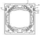
도 1 및 도 2에 도시된 바와 같이, 본 실시예에 의한 카메라 모듈은 인쇄회로기판(10), 베이스(20), 보빈(30), 커버부재(40)를 포함한다.1 and 2, the camera module according to the present embodiment includes a printed
인쇄회로기판(10)의 상측에는 이미지 센서(11)가 실장 되며, 상기 인쇄회로기판(10)의 상측에는 베이스(20)가 설치된다.An
상기 베이스(20)의 상기 이미지 센서(11)와 대면 되는 위치에는 적외선 차단 필터가 설치 되어, 상기 이미지 센서(11)에 적외선 파장 대역의 빛이 전달되는 것을 차단할 수 있다. 상기 베이스(20) 하측에 센서홀더를 추가로 구성하는 것도 가능하다. 본 실시예의 경우, 하측에 센서홀더 없이 하측 탄성부재(35)를 지지하기 위한 센서홀더와 일체로 구성된 베이스(20)를 가지는 구성을 예시로 설명한다.An infrared ray cutoff filter may be installed at a position of the
베이스(20)에는 터미널(21)이 설치되어, 일단은 인쇄회로기판(10)과 통전 가능하게 연결되고, 그 타단은 후술할 하측 탄성부재(35)와 솔더링으로 통전 가능하게 연결될 수 있다.The
터미널(21)은 금속재질로 설계에 따라 다양하게 구성될 수 있는데, 일 예로 하나의 부재가 적어도 2번 이상 절곡 형성되어 베이스(20)에 결합될 수도 있고, 베이스(20)에 인서트 사출될 수도 있다. 본 실시예의 경우에는 터미널(21)을 베이스(20)와 별도 부재로 형성하여 결합하는 것을 예시로 설명한다.The
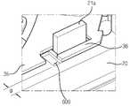
도 2 및 도 3은 제 1 실시예에 따른 터미널(21)과 하측 탄성부재(35)의 연결부를 도시한 도면이다.2 and 3 are views showing connection portions of the
도시된 바와 같이, 터미널(21)의 하측 탄성부재(35) 연결부에는 상기 하측 탄성부재(35)의 상측으로 관통 결합되는 단자부(21a)가 마련된다. 그리고, 상기 연결부의 하측 탄성부재(35)에는 상기 단자부(21a)의 주변을 감싸는 단자 연결부(36)가 형성될 수 있다.As shown in the figure, the connection portion of the lower
단자부(21a)는 터미널(21)과 한 몸을 가지도록 형성되며, 터미널(21)의 일단을 절곡하여 형성할 수 있다. 단자 연결부(36)는 상기 단자부(21a)의 폭과 길이에 대응되도록 하측 탄성부재(35)에 절개부로 형성할 수 있으며, 또는 홀로 형성할 수도 있다.The
상기 단자부(21a)와 단자 연결부(36)는 솔더부(S)에서 땜납에 의해 통전 가능하게 연결되어, 인쇄회로기판(10)을 통해 공급되는 전원을 상기 하측 탄성부재(35)를 통해 후술 할 코일(32)에 전달할 수 있다. 솔더부(S)는 베이스(20)의 상부면에 올려진 하측 탄성부재(35)의 상부면과 단자부(21a)의 접촉위치에 형성될 수 있다. 상기 솔더부(S)에 도포되는 땜납은 솔더부(S)이외의 공간 및 하측 탄성부재(35)의 표면을 오염시키지 않는 것이 좋다. 그러나 카메라 모듈의 소형화에 따라, 수작업으로 이루어지는 솔더링 작업 중에 작업자의 실수 등으로 땜납이 솔더부(S) 이외의 구간에 흘러 넘칠 수도 있다. 본 실시예는 이와 같이 흘러 넘치는 솔더를 최소화하기 위하여 솔더 차단부를 베이스(20)에 형성하는 것에 특징이 있으며, 이는 뒤에 구체적으로 설명한다.The
보빈(30)은 상기 베이스(20)의 상측에 상하 이동 가능하게 설치된다. 상기 보빈(30)의 초기 위치는 상기 베이스(20)의 상측면 또는, 미도시된 상부 프레임의 내측면 및 상기 베이스(20)와 상부 프레임 사이 공간부 중 어느 한 곳에 형성될 수 있다. 상기 보빈(30)의 바닥면에는 적어도 하나 이상의 보스가 돌출 형성될 수 있다. 상기 보스는 상기 베이스(20)와 초기 위치에서 면 접촉할 수 있다. 본 실시예에 따르면, 상기 보스는 상기 보빈(30)의 바닥면에 복수 개가 대칭이 되도록 돌출 형성되는 것이 좋으나, 비대칭 형성도 가능하다.The bobbin (30) is installed on the upper side of the base (20) so as to be movable up and down. The initial position of the
상기 보빈(30)의 외주면에는 코일(32)이 권선 되어, 상기 코일(32)에 전류가 흐를 경우, 상기 커버부재(40)에 설치된 마그네트(41)와의 전자기적 상호작용에 의해 보빈(30)이 도 1의 화살표 A 방향으로 왕복운동을 수행할 수 있다.A
상기 보빈(30)의 내주면에는 나사산이 형성되어 한 장 이상의 렌즈(34)가 설치되는 렌즈배럴(33)이 결합될 수 있다. 이를 한정하는 것은 아니며, 나사산 없이 상기 렌즈배럴(33)이 일체로 구성되거나 나사산 없는 렌즈배럴을 상기 보빈에 결합하는 것도 가능하다.A
커버부재(40)는 도 1에 도시된 바와 같이, 상기 베이스(20)의 상측에 배치되고, 상기 커버부재(40)의 내주면에는 마그네트(41)가 상기 코일(32)이 권선 된 보빈(30)과 대면 되도록 설치된다.1, a
상기 커버부재(40)는 도 1에 도시된 바와 같이, 카메라 모듈의 가장 바깥쪽 면을 형성할 수 있으나 이를 한정하는 것은 아니다. 경우에 따라 상기 커버부재(40)의 바깥쪽을 덮을 수 있도록 별도의 하우징 부재가 더 구비되는 것도 가능하다. 또한, 상기 커버부재는 금속재질로 형성될 수 있으며, 요크 기능을 수행할 수 있다.The
본 실시예에 따른 카메라 모듈은 보빈(30)의 왕복이동을 탄력 지지할 수 있도록 상측 탄성부재(미도시) 및 하측 탄성부재(35)가 설치될 수 있다. 상기 상측 및 하측 탄성부재는 커버부재(40) 또는 베이스에 일단이 결합되고 타단은 보빈(30)의 상단 및 하단에 연결될 수 있다. 하측 탄성부재는 보빈(30)에 권선된 코일(32)에 전원을 공급하는 터미널이 일체로 하측 탄성부재를 절곡하여 구성될 수 있다. 또는, 상기 하측 탄성부재에 별도의 터미널 단자를 통해 상기 인쇄회로기판과 전기적으로 연결될 수도 있다.The camera module according to the present embodiment may be provided with an upper elastic member (not shown) and a lower
상기 커버부재(40)와 하측 탄성부재 사이에는 스페이서가 개재될 수도 있다. 스페이서는 상기 하측 탄성부재를 상기 커버부재(40)에 대하여 절연하기 위해 설치하는 것으로, 스페이서 대신 상기 베이스(20)의 형상을 변경하여 사용하는 것도 가능하다.A spacer may be interposed between the
또한, 카메라 모듈의 외곽을 구성하는 커버부재(40)를 감싸도록 쉴드 캔과 같은 하우징 부재를 더 구비하는 것도 가능하다. 이 경우, 상기 하우징 부재는 상기 보빈(30) 내측에 배치되는 렌즈를 통해 외부 이미지가 상기 이미지 센서로 전달될 수 있도록, 상기 렌즈와 대응되는 크기의 렌즈 홀을 중앙에 구비하여 외부 이미지가 상기 통공을 통해 상기 이미지 센서(11)로 전달되도록 구성할 수 있다.It is also possible to further include a housing member such as a shield can to enclose the
하우징 부재는 금속 재질로 마련되어 전자기파 차폐를 수행할 수 있으나, 이를 한정하는 것은 아니며, 필요에 따라 수지재질로 카메라 모듈의 가장 바깥쪽을 구성하거나, 기타 금속재질로 형성하는 것도 가능하다.The housing member may be made of a metal material to perform electromagnetic wave shielding, but is not limited thereto. The housing member may be made of a resin material as the outermost part of the camera module, or may be formed of other metal material.
또한, 별도의 하우징 부재를 더 구비하지 않고, 하우징부재와 요크를 일체화하는 구성도 가능하다. 즉, 카메라 모듈의 사이즈를 줄이기 위해 요크를 감싸도록 하우징 부재를 구성하지 않고, 요크의 외측면은 노출시키고, 요크의 외측면과 동일면이 되도록 나머지 부분만 하우징부재를 구성하여 일체화할 수도 있다.Further, it is also possible to integrate the housing member and the yoke without providing a separate housing member. That is, the housing member may not be configured to enclose the yoke to reduce the size of the camera module, but the outer surface of the yoke may be exposed, and the housing member may be configured to be integral with the outer surface of the yoke.
한편, 도 1에 도시된 바와 같이, 제 1 실시예에 따른 카메라 모듈은 상기한 터미널(21)의 단자부(21a)와 단자 연결부(36)를 전기적으로 연결하는 솔더부(S)의 땜납이 흘러 넘치는 것을 방지하기 위한 솔더 차단부로 솔더 차단벽(100)이 설치될 수 있다.1, in the camera module according to the first embodiment, solder of a solder portion S electrically connecting the
도 2 및 도 3에 도시된 바와 같이 솔더 차단벽(100)은 단자부(21a)를 감싸도록 하측 탄성부재(35)에 절개되어 형성된 단자 연결부(36)의 개구부에 상측 방향으로 돌출 형성된다.As shown in FIGS. 2 and 3, the
또한, 솔더 차단벽(100)의 돌출 높이는 상기 하측 탄성부재(35)의 두께를 넘지 않도록 형성되거나 높게 형성되어, 상기 솔더 차단벽(100)이 과도하게 돌출되지 않도록 구성될 수 있다.The protrusion height of the
이와 같은 구성에 따르면, 도 2의 솔더부(S)에 투입된 땜납의 양이 설계치 이상으로 많아 흘러 넘치더라도, 상기 솔더 차단벽(100)에 의해 넘친 땜납이 하측 탄성부재(35)의 몸체 부근으로 넘치는 것을 방지할 수 있다. 따라서 땜납 오염에 따른 이물질이 카메라 모듈의 적외선 차단 필터 및/또는 이미지 센서 측을 오염시키지 않는다.According to such a configuration, even if the amount of solder injected into the solder portion S of FIG. 2 exceeds the designed value, the solder overflowed by the
한편, 솔더 차단벽(100)의 형상은 다양하게 구성할 수 있다.On the other hand, the shape of the
즉, 도 4에 도시된 제 2 실시예에 따른 솔더 차단부는 다중 차단벽(200)으로 형성될 수 있다. 다중 차단벽(200)은 하측 탄성부재(35)의 단자 연결부(36)의 개구부와 대응되는 제 1 차단벽(210)와 상기 단자 연결부(36)와 평행하며, 단자 연결부(36) 보다는 짧게 형성된 제 2 차단벽(220)을 포함할 수 있다. 제 1 차단벽(210)는 상기한 제 1 실시예에서의 솔더 차단벽(100)의 기능을 수행하고, 제 2 차단벽(220)은 상기 제 1 차단벽(210)와 함께 오목한 수용부를 구성하여, 흘러 넘치는 땜납이 베이스(20)의 측벽으로 흘러 넘치는 것을 방지할 수 있다. 한편, 제 1 및 제 2 차단부(210)(220)은 한 몸으로 형성될 수 있다.That is, the solder blocking portion according to the second embodiment shown in FIG. 4 may be formed as a
또한, 도 5에 도시된 제 3 실시예에 따른 솔더 차단부는 이중 차단벽(300)으로 형성될 수 있다. 상기 이중 차단벽(300)은 하측 탄성부재(35)의 단자 연결부(36)의 개구부와 대응되는 위치에 배치되며, 상기 솔더부(S)와 인접한 부분에 제 1 높이로 돌출 형성되는 1차 차단벽(310)과, 상기 제 1 높이보다 낮은 제 2 높이로 돌출 형성되는 2차 차단벽(320)을 포함할 수 있다. 이때, 상기 1차 차단벽(310)과 2차 차단벽(320)은 도시된 바와 같이 계단 형상으로 마련될 수 있다.In addition, the solder blocking portion according to the third embodiment shown in FIG. 5 may be formed as a
이때, 상기 제 1 높이는 상기 하측 탄성부재(35)의 두께보다 큰 값을 가지도록 형성될 수 있다. 이는 1차 차단벽(310)이 솔더부(S)와 근접된 위치에 배치되므로, 2차 차단벽(320)에 비해 상대적으로 더 많은 양의 땜납의 흘러 넘침을 차단하기 위함이다. 또한, 2차 차단벽(320)은 하측 탄성부재(35)의 두께와 대응되도록 형성될 수 있다.At this time, the first height may be greater than the thickness of the lower
도 6은 제 4 실시예에 따른 솔더 차단부는 일정 깊이(d)를 가지는 요홈인 솔더 차단 트랩(400)으로 형성될 수 있다. 이때, 요홈의 형상은 상기한 제 1 실시예에 따른 일정 높이로 돌출 형성된 솔더 차단벽(100)과 동일하나, 오목한 요홈 형상으로 형성된 점에서 차이가 있다. 이때, 상기 깊이(d)는 베이스(20)의 두께를 넘지 않도록 형성될 수 있다. 이와 같은 구성에 따르면, 상기 솔더부(S)에서 흘러 넘친 땜납이 상기 솔더 차단 트랩(400)의 오목한 내부 공간부에 수용되므로, 흘러 넘친 땜납이 하측 탄성부재(35) 주변을 오염시키지 않는다.6, the solder barrier portion according to the fourth embodiment may be formed of a
도 7은 제 5 실시예에 따른 솔더 차단부는 다중 솔더 차단 트랩(500)으로 마련될 수 있는데, 도시된 바와 같이 제 4 실시예와 같이 오목한 요홈으로 형성될 수 있다. 이때, 요홈의 형상은 상기한 제 2 실시예에 따른 일정 높이로 돌출 형성된 다중 차단벽(200)과 동일하나, 오목한 요홈 형상으로 형성된 점에서 차이가 있다. 제 4 실시예와 차이가 있는 부분은 흘러 넘친 땜납이 유동할 수 있는 내부 공간을 형성하여, 흘러 넘친 땜납이 솔더 차단 트랩(500)의 상측으로 돌출되는 것을 최대한 억제할 수 있다.7, the solder barrier portion according to the fifth embodiment may be formed as a multiple
즉, 다중 솔더 차단 트랩(500)은 하측 탄성부재(35)의 단자 연결부(36)의 개구부와 대응되는 제 1 트랩(510)과 상기 단자 연결부(36)와 평행하며, 단자 연결부(36) 보다는 짧게 형성된 제 2 트랩(520)을 포함할 수 있다. 제 1 트랩(510)은 상기한 제 4 실시예에서의 솔더 차단 트랩(400)의 기능을 수행하고, 제 2 트랩(520)은 상기 제 1 트랩(510)과 함께 오목한 수용부를 구성하여, 흘러 넘치는 땜납에 유동 공간을 부여할 수 있다.That is, the multiple
도 8은 제 6 실시예에 따른 솔더 차단부는 부분 솔더 차단 트랩(600)을 도시한 것으로, 제 4 실시예와 달리, 솔더 차단 트랩(600)의 위치를 베이스(20)의 외주면으로부터 일정 거리(g) 이격 시켜, 베이스(20)의 외주면 측으로 개구부를 형성하지 않도록 구성한 것에 차이가 있다. 이러한 구성에 따르면, 넘친 땜납이 베이스(20)의 외주면 측으로 흘러 넘치는 것이 차단될 수 있다.8 illustrates a partial
한편, 제 4 내지 제 6 실시예와 같이 오목한 형상으로 솔더 차단부를 형성하면, 이 오목한 부분을 통해 외부 이물이 유입될 우려가 있다. 따라서, 도시하지는 않았으나, 상기한 제 4 내지 제 6 실시예의 경우, 상기 베이스(20)의 상측으로 결합되는 조립 상대물에 상기 솔더 차단부와 대응되는 형상의 돌출 구조를 형성하여 조립할 수 있다.On the other hand, if the solder blocking portion is formed in a concave shape as in the fourth to sixth embodiments, external foreign matter may flow through the concave portion. Accordingly, although not shown, in the fourth to sixth embodiments, the protruding structure corresponding to the solder blocking portion may be formed on the assembly partner coupled to the upper side of the
예컨대, 도 1에 도시된 바와 같이, 베이스(20)의 상측에 조립되는 커버부재(40)의 상기 솔더 차단부와 대응되는 위치에 상기한 솔더 차단 트랩(400), 다중 솔더 차단 트랩(500) 및 부분 솔더 차단 트랩(600)과 대응되는 형상의 돌출 리브를 형성하여, 이물 유입을 차단하는 것이 가능하다.For example, as shown in FIG. 1, the
상기한 바와 같은 제 1 내지 제 6 실시예에 따른 솔더 차단부를 베이스(20)에 구성하면, 솔더부(S)의 땜납이 흘러 넘치는 것을 차단할 수 있어, 흘러 넘친 땜납에 의해 하측 탄성부재(35)가 오염되는 것을 방지할 수 있다.When the solder interrupting portions according to the first to sixth embodiments as described above are formed on the
이상에서 본 실시예에 따른 실시예들이 설명되었으나, 이는 예시적인 것에 불과하고, 당해 분야에서 통상적 지식을 가진 자라면 이로부터 다양한 변형 및 균등한 범위의 실시예가 가능하다는 점을 이해할 것이다. 따라서, 본 실시예의 진정한 기술적 보호 범위는 다음의 특허청구범위에 의해서 정해져야 할 것이다.
While the present invention has been particularly shown and described with reference to exemplary embodiments thereof, it is to be understood that the invention is not limited to the disclosed embodiments, but, on the contrary, is intended to cover various modifications and equivalent arrangements included within the spirit and scope of the appended claims. Therefore, the true scope of protection of the present embodiment should be defined by the following claims.
10; 인쇄회로기판11; 이미지 센서
20; 베이스30; 보빈
32; 코일35; 하측 탄성부재
36; 단자 결합부40; 홀더부재
100; 솔더 차단벽200; 다중 차단벽
300; 이중 차단벽400; 솔더 차단 트랩
500; 다중 솔더 차단 트랩600; 부분 솔더 차단 트랩10; A printed
20;
32;
36;
100; A
300; Double blocking
500; Multiple
Claims (5)
Translated fromKorean상기 인쇄회로기판 상측에 설치되는 베이스;
상기 베이스 상측에 왕복 이동 가능하게 설치되는 보빈;
상기 베이스에 고정되어, 상기 보빈을 지지하는 하측 탄성부재;
상기 베이스에 설치되어, 일단은 상기 인쇄회로기판과 통전 가능하게 연결되고, 타단은 상기 하측 탄성부재와 솔더부에서 통전 가능하게 연결되는 터미널; 및
상기 베이스에 설치되고, 상기 솔더부에서 흘러 넘친 땜납의 유동을 차단하는 솔더 차단부;를 포함하는 카메라 모듈.
A printed circuit board on which an image sensor is installed;
A base provided on the printed circuit board;
A bobbin installed to be reciprocatable above the base;
A lower elastic member fixed to the base and supporting the bobbin;
A terminal provided on the base, one end electrically connected to the printed circuit board, and the other end electrically connected to the lower elastic member and the solder portion; And
And a solder blocking portion provided on the base and blocking the flow of the solder flowing from the solder portion.
상기 베이스의 상측으로 돌출 형성되는 솔더 차단벽인 카메라 모듈.
The semiconductor device according to claim 1,
And a solder barrier wall protruding upward from the base.
동일 높이를 가지면, 상기 단자부를 감싸 오목홈부를 형성하는 제 1 및 제 2 차단벽과, 서로 다른 높이를 가지는 1차 및 2차 차단벽 중 어느 하나인 카메라 모듈.
The method according to claim 2,
The first and second blocking walls forming a concave groove portion around the terminal portion and having a same height, and first and second blocking walls having different heights.
일정 깊이의 솔더 차단 트랩인 카메라 모듈.
The semiconductor device according to claim 1,
A camera module that is a solder barrier trap with a certain depth.
적어도 하나 이상의 트랩이 연결된 다중 솔더 차단 트랩 및 베이스의 외부면과 일정 거리 이격 된 부분 솔더 차단 트랩 중 어느 하나인 카메라 모듈.
The method of claim 4, wherein the solder-
A plurality of solder barrier traps to which at least one trap is connected and a partial solder barrier trap that is spaced apart from the outer surface of the base by a distance.
Priority Applications (10)
| Application Number | Priority Date | Filing Date | Title |
|---|---|---|---|
| KR1020130133690AKR102136839B1 (en) | 2013-11-05 | 2013-11-05 | Camera module |
| US14/531,178US9380193B2 (en) | 2013-11-05 | 2014-11-03 | Camera module |
| CN201910717743.3ACN110365888B (en) | 2013-11-05 | 2014-11-05 | Camera module |
| CN201410617382.2ACN104618629B (en) | 2013-11-05 | 2014-11-05 | Camera module |
| US15/175,703US9591196B2 (en) | 2013-11-05 | 2016-06-07 | Camera module |
| US15/413,610US10212323B2 (en) | 2013-11-05 | 2017-01-24 | Camera module |
| US16/241,297US10721383B2 (en) | 2013-11-05 | 2019-01-07 | Camera module |
| US16/899,922US11165943B2 (en) | 2013-11-05 | 2020-06-12 | Camera module |
| KR1020200088328AKR102287985B1 (en) | 2013-11-05 | 2020-07-16 | Camera module |
| US17/490,594US11616897B2 (en) | 2013-11-05 | 2021-09-30 | Camera module |
Applications Claiming Priority (1)
| Application Number | Priority Date | Filing Date | Title |
|---|---|---|---|
| KR1020130133690AKR102136839B1 (en) | 2013-11-05 | 2013-11-05 | Camera module |
Related Child Applications (1)
| Application Number | Title | Priority Date | Filing Date |
|---|---|---|---|
| KR1020200088328ADivisionKR102287985B1 (en) | 2013-11-05 | 2020-07-16 | Camera module |
Publications (2)
| Publication Number | Publication Date |
|---|---|
| KR20150051772Atrue KR20150051772A (en) | 2015-05-13 |
| KR102136839B1 KR102136839B1 (en) | 2020-07-23 |
Family
ID=53389167
Family Applications (1)
| Application Number | Title | Priority Date | Filing Date |
|---|---|---|---|
| KR1020130133690AActiveKR102136839B1 (en) | 2013-11-05 | 2013-11-05 | Camera module |
Country Status (1)
| Country | Link |
|---|---|
| KR (1) | KR102136839B1 (en) |
Cited By (4)
| Publication number | Priority date | Publication date | Assignee | Title |
|---|---|---|---|---|
| KR20180098076A (en)* | 2017-02-24 | 2018-09-03 | 엘지이노텍 주식회사 | Lens driving device, camera module and optical apparatus |
| CN112631042A (en)* | 2021-01-20 | 2021-04-09 | 维沃移动通信有限公司 | Electronic device and method of assembling electronic device |
| US12282203B2 (en) | 2017-02-24 | 2025-04-22 | Lg Innotek Co., Ltd. | Lens driving device, camera module, and optical instrument |
| KR102832440B1 (en)* | 2024-01-09 | 2025-07-11 | (주)캠시스 | Base for voice coil motor and camera module |
Citations (5)
| Publication number | Priority date | Publication date | Assignee | Title |
|---|---|---|---|---|
| JP2004297282A (en)* | 2003-03-26 | 2004-10-21 | Mitsubishi Electric Corp | The camera module |
| KR20080111674A (en)* | 2007-06-19 | 2008-12-24 | 삼성전기주식회사 | Board for camera module and camera module using same |
| US20090278978A1 (en)* | 2008-05-09 | 2009-11-12 | Mitsumi Electric Co. Ltd. | Camera module comprising three members |
| US20100284081A1 (en)* | 2009-05-08 | 2010-11-11 | Gutierrez Roman C | Integrated lens barrel |
| US20120008221A1 (en)* | 2010-07-12 | 2012-01-12 | Lg Innotek Co., Ltd. | Voice coil motor |
- 2013
- 2013-11-05KRKR1020130133690Apatent/KR102136839B1/enactiveActive
Patent Citations (6)
| Publication number | Priority date | Publication date | Assignee | Title |
|---|---|---|---|---|
| JP2004297282A (en)* | 2003-03-26 | 2004-10-21 | Mitsubishi Electric Corp | The camera module |
| KR20080111674A (en)* | 2007-06-19 | 2008-12-24 | 삼성전기주식회사 | Board for camera module and camera module using same |
| US20090278978A1 (en)* | 2008-05-09 | 2009-11-12 | Mitsumi Electric Co. Ltd. | Camera module comprising three members |
| KR101012720B1 (en)* | 2008-05-09 | 2011-02-09 | 미쓰미덴기가부시기가이샤 | Camera module |
| US20100284081A1 (en)* | 2009-05-08 | 2010-11-11 | Gutierrez Roman C | Integrated lens barrel |
| US20120008221A1 (en)* | 2010-07-12 | 2012-01-12 | Lg Innotek Co., Ltd. | Voice coil motor |
Cited By (5)
| Publication number | Priority date | Publication date | Assignee | Title |
|---|---|---|---|---|
| KR20180098076A (en)* | 2017-02-24 | 2018-09-03 | 엘지이노텍 주식회사 | Lens driving device, camera module and optical apparatus |
| US12282203B2 (en) | 2017-02-24 | 2025-04-22 | Lg Innotek Co., Ltd. | Lens driving device, camera module, and optical instrument |
| CN112631042A (en)* | 2021-01-20 | 2021-04-09 | 维沃移动通信有限公司 | Electronic device and method of assembling electronic device |
| CN112631042B (en)* | 2021-01-20 | 2021-09-24 | 维沃移动通信有限公司 | Electronic equipment and method of assembly of electronic equipment |
| KR102832440B1 (en)* | 2024-01-09 | 2025-07-11 | (주)캠시스 | Base for voice coil motor and camera module |
Also Published As
| Publication number | Publication date |
|---|---|
| KR102136839B1 (en) | 2020-07-23 |
Similar Documents
| Publication | Publication Date | Title |
|---|---|---|
| US11165943B2 (en) | Camera module | |
| US20250035950A1 (en) | Camera module | |
| US11616897B2 (en) | Camera module | |
| KR102214331B1 (en) | Camera module | |
| US20150260948A1 (en) | Lens driving device, camera device, and electronic apparatus | |
| KR20150051772A (en) | Camera module | |
| KR20120053838A (en) | Voice coil motor | |
| KR102704763B1 (en) | Lens moving unit and camera module having the same | |
| KR102287985B1 (en) | Camera module | |
| KR20170062437A (en) | Voice coil motor | |
| KR102519158B1 (en) | Camera module | |
| KR101959541B1 (en) | Voice coil motor | |
| KR101813277B1 (en) | Voice coil motor | |
| KR20140076819A (en) | Camera Module | |
| KR101794357B1 (en) | Camera Module | |
| KR102063980B1 (en) | Voice coil motor | |
| KR20160080263A (en) | Lens driving unit and camera module including the same | |
| KR20200004902A (en) | Voice coil motor | |
| KR20190031218A (en) | Voice coil motor | |
| KR20150064966A (en) | Camera module |
Legal Events
| Date | Code | Title | Description |
|---|---|---|---|
| PA0109 | Patent application | Patent event code:PA01091R01D Comment text:Patent Application Patent event date:20131105 | |
| PG1501 | Laying open of application | ||
| A201 | Request for examination | ||
| PA0201 | Request for examination | Patent event code:PA02012R01D Patent event date:20181030 Comment text:Request for Examination of Application Patent event code:PA02011R01I Patent event date:20131105 Comment text:Patent Application | |
| E902 | Notification of reason for refusal | ||
| PE0902 | Notice of grounds for rejection | Comment text:Notification of reason for refusal Patent event date:20191018 Patent event code:PE09021S01D | |
| E701 | Decision to grant or registration of patent right | ||
| PE0701 | Decision of registration | Patent event code:PE07011S01D Comment text:Decision to Grant Registration Patent event date:20200417 | |
| PA0107 | Divisional application | Comment text:Divisional Application of Patent Patent event date:20200716 Patent event code:PA01071R01D | |
| PR0701 | Registration of establishment | Comment text:Registration of Establishment Patent event date:20200716 Patent event code:PR07011E01D | |
| PR1002 | Payment of registration fee | Payment date:20200717 End annual number:3 Start annual number:1 | |
| PG1601 | Publication of registration | ||
| PR1001 | Payment of annual fee | Payment date:20230612 Start annual number:4 End annual number:4 | |
| PR1001 | Payment of annual fee | Payment date:20240617 Start annual number:5 End annual number:5 | |
| PR1001 | Payment of annual fee | Payment date:20250616 Start annual number:6 End annual number:6 |