KR20150038513A - Multiple sets of attribute fields within a single page table entry - Google Patents
Multiple sets of attribute fields within a single page table entryDownload PDFInfo
- Publication number
- KR20150038513A KR20150038513AKR20157005315AKR20157005315AKR20150038513AKR 20150038513 AKR20150038513 AKR 20150038513AKR 20157005315 AKR20157005315 AKR 20157005315AKR 20157005315 AKR20157005315 AKR 20157005315AKR 20150038513 AKR20150038513 AKR 20150038513A
- Authority
- KR
- South Korea
- Prior art keywords
- processing unit
- memory
- access
- chunk
- page table
- Prior art date
- Legal status (The legal status is an assumption and is not a legal conclusion. Google has not performed a legal analysis and makes no representation as to the accuracy of the status listed.)
- Granted
Links
Images
Classifications
- G—PHYSICS
- G06—COMPUTING OR CALCULATING; COUNTING
- G06F—ELECTRIC DIGITAL DATA PROCESSING
- G06F12/00—Accessing, addressing or allocating within memory systems or architectures
- G06F12/02—Addressing or allocation; Relocation
- G06F12/08—Addressing or allocation; Relocation in hierarchically structured memory systems, e.g. virtual memory systems
- G06F12/10—Address translation
- G06F12/1009—Address translation using page tables, e.g. page table structures
- G—PHYSICS
- G06—COMPUTING OR CALCULATING; COUNTING
- G06F—ELECTRIC DIGITAL DATA PROCESSING
- G06F12/00—Accessing, addressing or allocating within memory systems or architectures
- G06F12/14—Protection against unauthorised use of memory or access to memory
- G06F12/1416—Protection against unauthorised use of memory or access to memory by checking the object accessibility, e.g. type of access defined by the memory independently of subject rights
- G06F12/145—Protection against unauthorised use of memory or access to memory by checking the object accessibility, e.g. type of access defined by the memory independently of subject rights the protection being virtual, e.g. for virtual blocks or segments before a translation mechanism
- G—PHYSICS
- G06—COMPUTING OR CALCULATING; COUNTING
- G06F—ELECTRIC DIGITAL DATA PROCESSING
- G06F2212/00—Indexing scheme relating to accessing, addressing or allocation within memory systems or architectures
- G06F2212/65—Details of virtual memory and virtual address translation
- G06F2212/656—Address space sharing
- Y—GENERAL TAGGING OF NEW TECHNOLOGICAL DEVELOPMENTS; GENERAL TAGGING OF CROSS-SECTIONAL TECHNOLOGIES SPANNING OVER SEVERAL SECTIONS OF THE IPC; TECHNICAL SUBJECTS COVERED BY FORMER USPC CROSS-REFERENCE ART COLLECTIONS [XRACs] AND DIGESTS
- Y02—TECHNOLOGIES OR APPLICATIONS FOR MITIGATION OR ADAPTATION AGAINST CLIMATE CHANGE
- Y02D—CLIMATE CHANGE MITIGATION TECHNOLOGIES IN INFORMATION AND COMMUNICATION TECHNOLOGIES [ICT], I.E. INFORMATION AND COMMUNICATION TECHNOLOGIES AIMING AT THE REDUCTION OF THEIR OWN ENERGY USE
- Y02D10/00—Energy efficient computing, e.g. low power processors, power management or thermal management
Landscapes
- Engineering & Computer Science (AREA)
- Theoretical Computer Science (AREA)
- Physics & Mathematics (AREA)
- General Engineering & Computer Science (AREA)
- General Physics & Mathematics (AREA)
- Computer Security & Cryptography (AREA)
- Memory System Of A Hierarchy Structure (AREA)
- Memory System (AREA)
Abstract
Translated fromKoreanDescription
Translated fromKorean본 개시물은 일반적으로 컴퓨팅에 관한 것이고, 보다 상세하게는 가상 메모리 어드레스 공간을 물리 메모리 어드레스 공간으로 맵핑하기 위한 기법들에 관한 것이다.[0002] This disclosure relates generally to computing, and more particularly to techniques for mapping a virtual memory address space to a physical memory address space.
통상의 컴퓨팅 시스템들은, 물리 메모리로부터 판독하고 물리 메모리에 기록하는, 중앙 프로세싱 유닛들 (CPUs) 및 그래픽스 프로세싱 유닛들 (GPUs) 과 같은 다중 프로세싱 유닛들을 포함한다. 디바이스의 다양한 프로세싱 유닛들은, 클라이언트들에 의해 실행되는 어플리케이션들이 인접 물리 메모리 공간 한쪽으로 설정되어야 하지 않으면서 인접 가상 어드레스 공간에 할당될 수 있도록 가상 어드레싱 스킴들을 구현할 수도 있다. 각각의 프로세싱 유닛은 통상적으로 가상 메모리 어드레스를 물리 메모리에서의 물리 어드레스로 변환하기 위해 메모리 관리 유닛 (MMU) 를 갖는다. 필요한 물리 어드레스로의 가상 어드레스 맵핑을 수행하기 위해, 각각의 MMU 는 시스템 메모리에 별도의 페이지 테이블을 유지하며, 이러한 별도의 페이지 테이블의 각각은 사이즈가 수 메가바이트일 수 있다.Common computing systems include multiple processing units, such as central processing units (CPUs) and graphics processing units (GPUs), that read from and write to physical memory. The various processing units of the device may implement virtual addressing schemes so that applications executed by clients may be allocated to the adjacent virtual address space without having to be set to one side of the adjacent physical memory space. Each processing unit typically has a memory management unit (MMU) for converting a virtual memory address into a physical address in physical memory. To perform a virtual address mapping to the required physical address, each MMU maintains a separate page table in the system memory, and each of these separate page tables may be several megabytes in size.
일반적으로, 본 개시물에 기재된 기법들은 물리 어드레스로의 가상 어드레스 맵핑을 구현하는 컴퓨팅 디바이스들에 관련된다. 본 개시물의 기법들에 의하면, 2 이상의 프로세싱 유닛들은 가상 어드레스들을 물리 어드레스들로 맵핑하기 위한 공통 페이지 테이블을 공유할 수도 있다. 공통 페이지 테이블의 페이지 테이블 엔트리들은 제 1 프로세싱 유닛에 대한 속성 세트, 제 2 프로세싱 유닛에 대한 속성 세트와 같은 속성 필드들의 다중 세트들 뿐만 아니라 다른 속성 세트들을 포함할 수도 있다. 속성 필드들의 다중 세트들을 사용하여, 2 이상의 프로세싱 유닛들에 대한 속성들이 개별적으로 관리될 수도 있다. 예를 들어, 본 개시물에 기재된 기법들은 제 1 및 제 2 프로세싱 유닛들의 판독/기록 액세스의 개별적인 관리를 허용할 수도 있어서, 일 프로세싱 유닛으로의 판독/기록 액세스가 제 2 프로세싱 유닛으로의 판독/기록 액세스와 상이하다.In general, the techniques described in this disclosure relate to computing devices that implement virtual address mapping to physical addresses. According to the teachings of the present disclosure, two or more processing units may share a common page table for mapping virtual addresses to physical addresses. The page table entries of the common page table may include different sets of attributes as well as multiple sets of attribute fields, such as an attribute set for the first processing unit, an attribute set for the second processing unit. Using multiple sets of attribute fields, attributes for two or more processing units may be managed separately. For example, the techniques described in this disclosure may allow for separate management of read / write accesses of the first and second processing units, so that read / write access to one processing unit may be performed by a read / write access to the second processing unit, And is different from the write access.
일 예에 따라, 장치는 제 1 프로세싱 유닛, 제 2 프로세싱 유닛, 및 메모리를 포함한다. 메모리는 제 1 프로세싱 유닛 및 제 2 프로세싱 유닛에 공통이고, 작업 (job) 에 의해 액세스된 메모리 청크들에 대한 물리 메모리 어드레스들로의 가상 메모리 어드레스들 맵핑을 저장하는 공통 페이지 테이블을 저장한다. 메모리는 또한 제 1 프로세싱 유닛 및 제 2 프로세싱 유닛이 메모리 청크들의 메모리 청크에 액세스하는데 사용하는, 공통 페이지 테이블 내의 페이지 엔트리를 저장하며, 페이지 엔트리는 제 1 프로세싱 유닛에 의한 메모리 청크의 액세스가능성을 정의하는 속성 비트들의 제 1 세트, 제 2 프로세싱 유닛에 의한 동일한 메모리 청크의 액세스가능성을 정의하는 속성 비트들의 제 2 세트, 및 메모리 청크의 물리 어드레스를 정의하는 물리 어드레스 비트들을 포함한다.According to one example, an apparatus includes a first processing unit, a second processing unit, and a memory. The memory is common to the first processing unit and the second processing unit and stores a common page table storing virtual memory address mappings to physical memory addresses for the memory chunks accessed by the job. The memory also stores a page entry in the common page table that the first processing unit and the second processing unit use to access the memory chunks of memory chunks, and the page entry defines the accessibility of the memory chunk by the first processing unit A second set of attribute bits defining accessibility of the same memory chunk by the second processing unit, and physical address bits defining a physical address of the memory chunk.
또 다른 예에 따라, 방법은 제 1 프로세싱 유닛에 의해, 메모리에 저장된 공통 페이지 테이블을 사용하여 가상 메모리 어드레스를 물리 메모리 어드레스로 변환하는 단계; 제 1 프로세싱 유닛에 의해, 물리 메모리 어드레스에 의해 식별된 메모리 청크에 액세스하는 단계; 제 2 프로세싱 유닛에 의해, 가상 메모리 어드레스를 메모리에 저장된 공통 페이지 테이블을 사용하여 물리 메모리 어드레스로 변환하는 단계; 및 제 2 프로세싱 유닛에 의해, 물리 메모리 어드레스에 의해 식별된 메모리 청크에 액세스하는 단계를 포함한다. 공통 페이지 테이블은 제 1 프로세싱 유닛 및 제 2 프로세싱 유닛에 공통이고, 작업에 의해 액세스된 메모리 청크들에 대한 물리 메모리 어드레스들로의 가상 메모리 어드레스들 맵핑을 저장한다. 공통 페이지 테이블은 제 1 프로세싱 유닛 및 제 2 프로세싱 유닛이 메모리 청크에 액세스하는데 사용하는 페이지 엔트리를 포함하며, 페이지 엔트리는 제 1 프로세싱 유닛에 의한 메모리 청크의 액세스가능성을 정의하는 속성 비트들의 제 1 세트, 제 2 프로세싱 유닛에 의한 동일한 메모리 청크의 액세스가능성을 정의하는 속성 비트들의 제 2 세트, 및 메모리 청크의 물리 어드레스를 정의하는 물리 어드레스 비트들을 포함한다.According to yet another example, the method comprises: converting, by a first processing unit, a virtual memory address to a physical memory address using a common page table stored in the memory; Accessing, by the first processing unit, the memory chunk identified by the physical memory address; Converting, by the second processing unit, the virtual memory address into a physical memory address using a common page table stored in the memory; And accessing, by the second processing unit, the memory chunk identified by the physical memory address. The common page table is common to the first processing unit and the second processing unit and stores virtual memory addresses mappings to physical memory addresses for memory chunks accessed by the task. Wherein the common page table comprises a page entry used by the first processing unit and the second processing unit to access the memory chunk and the page entry comprises a first set of attribute bits defining accessibility of the memory chunk by the first processing unit, A second set of attribute bits defining accessibility of the same memory chunk by the second processing unit, and physical address bits defining a physical address of the memory chunk.
또 다른 예에 따라, 장치는 제 1 프로세싱 수단, 제 2 프로세싱 수단, 및 메모리를 포함한다. 제 1 프로세싱 수단은, 메모리에 저장된 공통 테이블을 사용하여 가상 메모리 어드레스를 물리 메모리 어드레스로 변환하기 위한 수단, 및 물리 메모리 어드레스에 의해 식별된 메모리 청크에 액세스하기 위한 수단을 포함하고, 제 2 프로세싱 수단은, 메모리에 저장된 공통 페이지 테이블을 사용하여 가상 메모리 어드레스를 물리 메모리 어드레스로 변환하기 위한 수단, 및 물리 메모리 어드레스에 의해 식별된 메모리 청크에 액세스하기 위한 수단을 포함한다. 공통 페이지 테이블은 제 1 프로세싱 수단 및 제 2 프로세싱 수단에 공통이고, 작업에 의해 액세스된 메모리 청크들에 대한 물리 메모리 어드레스들로의 가상 메모리 어드레스들 맵핑을 저장한다. 공통 페이지 테이블은 제 1 프로세싱 수단 및 제 2 프로세싱 수단이 메모리 청크에 액세스하는데 사용하는 페이지 엔트리를 포함하며, 페이지 엔트리는 제 1 프로세싱 수단에 의한 메모리 청크의 액세스가능성을 정의하는 속성 비트들의 제 1 세트, 제 2 프로세싱 수단에 의한 동일한 메모리 청크의 액세스가능성을 정의하는 속성 비트들의 제 2 세트, 및 메모리 청크의 물리 어드레스를 정의하는 물리 어드레스 비트들을 포함한다.According to yet another example, an apparatus includes a first processing means, a second processing means, and a memory. The first processing means comprises means for converting the virtual memory address to a physical memory address using a common table stored in the memory and means for accessing the memory chunk identified by the physical memory address, Comprises means for converting a virtual memory address to a physical memory address using a common page table stored in the memory and means for accessing the memory chunk identified by the physical memory address. The common page table is common to the first processing means and the second processing means and stores virtual memory address mapping to physical memory addresses for memory chunks accessed by the task. Wherein the common page table comprises a page entry used by the first processing means and the second processing means to access the memory chunk and the page entry comprises a first set of attribute bits defining accessibility of the memory chunk by the first processing means A second set of attribute bits defining accessibility of the same memory chunk by the second processing means, and physical address bits defining the physical address of the memory chunk.
또 다른 예에 따라, 컴퓨터 판독가능 저장 매체는, 실행될 때, 제 1 프로세싱 유닛 및 제 2 프로세싱 유닛으로 하여금, 제 1 프로세싱 유닛에 의해, 메모리에 저장된 공통 페이지 테이블을 사용하여 가상 메모리 어드레스를 물리 메모리 어드레스로 변환하게 하고; 제 1 프로세싱 유닛에 의해, 물리 메모리 어드레스에 의해 식별된 메모리 청크에 액세스하게 하고; 제 2 프로세싱 유닛에 의해, 메모리에 저장된 공통 페이지 테이블을 사용하여 가상 메모리 어드레스를 물리 메모리 어드레스로 변환하게 하고; 제 2 프로세싱 유닛에 의해, 물리 메모리 어드레스에 의해 식별된 메모리 청크에 액세스하게 하는 명령들을 저장한다. 공통 페이지 테이블은 제 1 프로세싱 유닛 및 제 2 프로세싱 유닛에 공통이고, 작업에 의해 액세스된 메모리 청크들에 대한 물리 메모리 어드레스들로의 가상 메모리 어드레스들 맵핑을 저장한다. 공통 페이지 테이블은 제 1 프로세싱 유닛 및 제 2 프로세싱 유닛이 메모리 청크에 액세스하는데 사용하는 페이지 엔트리를 포함한다. 페이지 엔트리는 제 1 프로세싱 유닛에 의한 메모리 청크의 액세스가능성을 정의하는 속성 비트들의 제 1 세트, 제 2 프로세싱 유닛에 의한 동일한 메모리 청크의 액세스가능성을 정의하는 속성 비트들의 제 2 세트, 및 메모리 청크의 물리 어드레스를 정의하는 물리 어드레스 비트들을 포함한다.According to another example, a computer-readable storage medium, when executed, causes a first processing unit and a second processing unit to perform the steps of, by a first processing unit, Address; Access, by the first processing unit, the memory chunk identified by the physical memory address; Cause the second processing unit to use the common page table stored in the memory to convert the virtual memory address to a physical memory address; By the second processing unit, instructions to access the memory chunk identified by the physical memory address. The common page table is common to the first processing unit and the second processing unit and stores virtual memory addresses mappings to physical memory addresses for memory chunks accessed by the task. The common page table includes page entries that the first processing unit and the second processing unit use to access memory chunks. The page entry includes a first set of attribute bits defining accessibility of the memory chunk by the first processing unit, a second set of attribute bits defining accessibility of the same memory chunk by the second processing unit, And physical address bits that define a physical address.
도 1 은 본 개시물에 기재된 물리 메모리 어드레스로의 가상 메모리 어드레스 맵핑 기법들을 구현하도록 구성된 컴퓨팅 디바이스의 일 예를 나타낸다.
도 2 는 본 개시물에 기재된 물리 메모리 어드레스로의 가상 메모리 어드레스 맵핑 기법들을 구현하도록 구성된 컴퓨팅 디바이스의 또 다른 예를 나타낸다.
도 3 은 본 개시물에 기재된 기법들에 따라 단일 페이지 테이블 엔트리 내에 속성 필드들의 다중 세트들을 갖는 공통 페이지 테이블의 개념적 다이어그램을 나타낸다.
도 4 는 본 개시물에 기재된 물리 메모리 어드레스로의 가상 메모리 어드레스 맵핑 기법들을 도시하는 플로우 다이어그램을 나타낸다.1 illustrates an example of a computing device configured to implement virtual memory address mapping techniques to physical memory addresses described in this disclosure.
Figure 2 illustrates another example of a computing device configured to implement virtual memory address mapping techniques to physical memory addresses described in this disclosure.
Figure 3 shows a conceptual diagram of a common page table with multiple sets of attribute fields in a single page table entry according to the techniques described in this disclosure.
Figure 4 shows a flow diagram illustrating virtual memory address mapping techniques to physical memory addresses described in this disclosure.
일반적으로, 본 개시물에 기재된 기법들은, 본 개시물에서 가상-투-물리 맵핑으로서 또한 지칭되는, 물리 어드레스로의 가상 어드레스 맵핑을 구현하는 컴퓨팅 디바이스들에 관련된다. 특히, 본 개시물에 기재된 기법들은 2 이상의 프로세싱 유닛들에 의해 공유될 수 있는 공통 페이지 테이블로 지향된다. 공통 페이지 테이블의 페이지 테이블 엔트리들은 제 1 프로세싱 유닛에 대한 속성 세트, 제 2 프로세싱 유닛에 대한 속성 세트와 같은 속성 필드들의 다중 세트들 뿐만 아니라 다른 속성 세트들을 포함할 수도 있다. 속성 필드들의 다중 세트들을 사용하여, 2 이상의 프로세싱 유닛들에 대한 속성들이 개별적으로 관리될 수도 있다. 예를 들어, 일 프로세싱 유닛에 대한 판독/기록 액세스가 제 2 프로세싱 유닛에 대한 판독/기록 액세스와 상이할 수도 있다.Generally, the techniques described in this disclosure relate to computing devices that implement virtual address mapping to physical addresses, also referred to as virtual-to-physical mapping in this disclosure. In particular, the techniques described in this disclosure are directed to a common page table that can be shared by two or more processing units. The page table entries of the common page table may include different sets of attributes as well as multiple sets of attribute fields, such as an attribute set for the first processing unit, an attribute set for the second processing unit. Using multiple sets of attribute fields, attributes for two or more processing units may be managed separately. For example, the read / write access to one processing unit may be different from the read / write access to the second processing unit.
중앙 프로세싱 유닛들 (CPUs) 및 그래픽스 프로세싱 유닛들 (GPUs) 은 물리 메모리에 액세싱하는 것 (물리 메모리로부터 데이터를 판독하고 물리 메모리에 데이터를 저장하는 것) 을 필요로 한다. 데이터를 판독 또는 기록하기 위해, 프로세싱 유닛은 물리 메모리 내의 위치에 액세스 하며, 여기서 데이터는 그 메모리 내의 위치에 대한 물리 어드레스로 판독되거나 기록된다. 하지만, 프로세싱 유닛이 메모리 청크들 (즉, 데이터가 기록되거나 판독될 수 있는 물리 메모리의 위치들) 모두에 대해 물리 어드레스들을 관리하는 것은 어렵다. 이러한 어려움을 극복하기 위해, 프로세싱 유닛은 가상 어드레싱을 사용할 수도 있다. 가상 어드레싱에 있어서, 프로세싱 유닛 상에서 실행하는 어플리케이션들 (즉, 클라이언트들) 은 인접 가상 메모리 어드레스들에 할당된다. 어플리케이션은 상이한 프로세싱 유닛들 상에서 실행하는 상이한 작업들을 갖는 다중 작업들을 포함할 수도 있다. 프로세싱 유닛들의 각각은 각각의 메모리 관리 유닛들 (MMUs) 을 포함한다. 프로세싱 유닛들의 각각의 MMU 는 물리 메모리 어드레스들로서 또한 지칭되는 실제 메모리 어드레스들을 가상 메모리 어드레스들로부터 결정하는 것으로 태스킹된다.Central Processing Units (CPUs) and Graphics Processing Units (GPUs) require accessing physical memory (reading data from physical memory and storing data in physical memory). To read or write data, the processing unit accesses a location in physical memory, where the data is read or written to a physical address for the location in that memory. However, it is difficult for the processing unit to manage physical addresses for all of the memory chunks (i. E., The locations of physical memory where data can be written to or read from). To overcome this difficulty, the processing unit may use virtual addressing. In virtual addressing, applications executing on the processing unit (i. E., Clients) are assigned to adjacent virtual memory addresses. An application may include multiple tasks with different tasks executing on different processing units. Each of the processing units includes respective memory management units (MMUs). Each MMU of the processing units is tasked with determining from the virtual memory addresses actual memory addresses, also referred to as physical memory addresses.
예를 들어, MMU 는 변환 색인 버퍼 (TLB) 로서 지칭되는 캐시를 포함한다. TLB 는 선택된 메모리 청크들, 예컨대 최근에 액세스된 메모리 청크들 또는 빈번하게 액세스된 메모리 청크들에 대한 가상-투-물리 맵핑을 저장한다. 메모리 청크에 액세스하기 위해, 프로세싱 유닛은 그 메모리 청크에 대한 가상 메모리 어드레스를 MMU 에 공급한다. 이어서, MMU 는 TLB 에 액세스하여 그 메모리 청크에 대한 물리 메모리 어드레스를 식별한다. TLB 에서 맵핑이 이용가능할 때 (TLB 히트로서 지칭됨), MMU 는 그 후 물리 메모리 액세스를 사용하여 메모리에 액세스한다. 대안으로, MMU 는 그 후 물리 메모리 어드레스를 사용하여 메모리 청크에 액세스하는 프로세싱 유닛의 상이한 유닛 또는 모듈에 물리 메모리를 공급한다.For example, the MMU includes a cache referred to as a translation index buffer (TLB). The TLB stores virtual-to-physical mappings for selected memory chunks, such as recently accessed memory chunks or frequently accessed memory chunks. To access the memory chunk, the processing unit supplies a virtual memory address for that memory chunk to the MMU. The MMU then accesses the TLB and identifies the physical memory address for that memory chunk. When a mapping is available in the TLB (referred to as a TLB hit), the MMU then accesses the memory using physical memory access. Alternatively, the MMU then uses the physical memory address to provide physical memory to a different unit or module of the processing unit that accesses the memory chunk.
일부 경우들에서, TLB 는 가상 메모리 어드레스를 위한 맵핑을 포함하지 않을 수도 있다 (TLB 미스로서 지칭됨). 예를 들어, 프로세싱 유닛은 물리 어드레스가 TLB 에 의해 저장된 페이지 엔트리들에 포함되지 않는 메모리 청크에 액세할 필요가 있을 수도 있는데, 이는 메모리 청크가 최근에 액세스되거나 빈번하게 액세스된 메모리 청크가 아니기 때문이다. 이것이 발생할 때, 프로세싱 유닛은 시스템 메모리에 저장된 페이지 테이블에 액세스한다.In some cases, the TLB may not include a mapping for a virtual memory address (referred to as a TLB miss). For example, the processing unit may need to access a memory chunk whose physical address is not included in page entries stored by the TLB, because the memory chunk is not recently accessed or accessed frequently . When this occurs, the processing unit accesses the page table stored in the system memory.
페이지 테이블은 양자가 가상 메모리 어드레스들을 물리 메모리 어드레스들에 맵핑하는 페이지 엔트리들을 저장한다는 점에서 TLB 와 유사하다. 페이지 테이블에서 또는 TLB 에서, 하나의 페이지 테이블 엔트리는 하나의 가상 메모리 어드레스를 하나의 물리 메모리 어드레스에 맵핑한다. 하지만, 페이지 테이블은 프로세싱 유닛의 MMU 내에 국부적으로 저장되는 TLB 와 대조적으로 시스템 메모리에 저장된다. 또한, 페이지 테이블은 TLB 처럼 페이지 엔트리들의 제한된 수 대신 프로세싱 유닛에 대한 전체 가상-투-물리 어드레스 맵핑을 저장하기 때문에, 페이지 테이블의 사이즈가 일반적으로 TLB 의 사이즈보다 훨씬 크다. 가령, 페이지 테이블의 사이즈는 메가바이트 범위일 수도 있다.The page table is similar to a TLB in that both store page entries that map virtual memory addresses to physical memory addresses. In a page table or in a TLB, one page table entry maps one virtual memory address to one physical memory address. However, the page table is stored in the system memory as opposed to the TLB stored locally in the MMU of the processing unit. Also, because the page table stores the entire virtual-to-physical address mapping for the processing unit instead of a limited number of page entries, such as a TLB, the page table size is typically much larger than the size of the TLB. For example, the size of the page table may be in the megabyte range.
일부 기법들에서, 시스템 메모리는 프로세싱 유닛들의 각각에 대한 대응 페이지 테이블들을 저장한다. 예를 들어, 시스템 메모리는 CPU 에 대한 페이지 테이블을 저장하고, 또 다른, GPU 에 대한 별도의 페이지 테이블을 저장한다. 하지만, 일부 경우들에서, 이러한 상이한 페이지 테이블들은 동일한 페이지 테이블 엔트리들을 포함한다. 따라서, CPU 페이지 테이블에서의 다중 페이지 테이블 엔트리들은 GPU 페이지 테이블에서의 페이지 테이블 엔트리들과 동일한 것이 가능할 수도 있다. 예를 들어, CPU 페이지 테이블에서의 페이지 테이블 엔트리는 하나의 가상 메모리 어드레스를 물리 메모리 어드레스로 맵핑할 수도 있고, GPU 페이지 테이블에서의 페이지 테이블 엔트리는 동일한 가상 메모리 어드레스를 동일한 물리 메모리 어드레스로 맵핑할 수도 있다.In some techniques, the system memory stores corresponding page tables for each of the processing units. For example, system memory stores the page table for the CPU and another page table for the GPU. However, in some cases, these different page tables include the same page table entries. Thus, the multipage table entries in the CPU page table may be the same as the page table entries in the GPU page table. For example, a page table entry in the CPU page table may map one virtual memory address to a physical memory address, and a page table entry in the GPU page table may map the same virtual memory address to the same physical memory address have.
일 예로서, CPU 상에서 실행하는 오퍼레이팅 시스템은 인접 가상 메모리 어드레스를 어플리케이션에 할당하는 것으로 태스킹될 수도 있다. 어플리케이션은 CPU 상에서 실행하는 일부 작업들 및 GPU 상에서 실행하는 일부 작업들을 갖는, 복수의 작업들 또는 태스크들을 포함할 수도 있다. 오퍼레이팅 시스템은 또한 가상 메모리 어드레스와 물리 메모리 어드레스 사이의 맵핑을 페이지 테이블에 저장할 수도 있다. 오퍼레이팅 시스템은 가상 메모리 어드레스들을 할당하는 것 및 CPU 및 GPU 의 양자에 대해 이러한 가상 메모리 어드레스들의 물리 어드레스들로의 맵핑으로 태스킹되기 때문에, 오퍼레이팅 시스템은 CPU 및 GPU 의 양자에 대한 가상-투-물리 맵핑을 저장하는 공통 페이지 테이블을 생성할 수도 있다.As an example, an operating system running on a CPU may be tasked with assigning an adjacent virtual memory address to an application. An application may include multiple tasks or tasks, with some tasks running on the CPU and some tasks running on the GPU. The operating system may also store the mapping between the virtual memory address and the physical memory address in a page table. Because the operating system is tasked with both assigning virtual memory addresses and mapping these virtual memory addresses to physical addresses for both the CPU and the GPU, the operating system can use virtual-to-physical mapping for both the CPU and the GPU May be generated.
그러한 공통 페이지 테이블을 공유하는 CPU 및 GPU 에서는 이점들이 있을 수도 있다. 예를 들어, 시스템 메모리가 중복 페이지 테이블 엔트리들을 저장하는 대신, 시스템 메모리가 CPU 페이지 테이블 및 GPU 페이지 테이블에서 동일한 페이지 테이블 엔트리들에 대한 단일 페이지 엔트리를 저장할 수도 있으며, 이는 메모리 절약을 야기한다. 게다가, 이러한 동일한 페이지 테이블 엔트리들에 대한 하나의 페이지 엔트리가 있기 때문에, 2 개의 동일한 페이지 테이블 엔트리들 대신 단일 페이지 테이블 엔트리를 업데이트하는 것이 계산적으로 더 효율적일 수도 있다.CPUs and GPUs sharing such a common page table may have advantages. For example, instead of system memory storing redundant page table entries, system memory may store a single page entry for the same page table entries in the CPU page table and the GPU page table, which results in memory savings. In addition, since there is one page entry for these same page table entries, updating a single page table entry instead of two identical page table entries may be computationally more efficient.
일부 종래 기법들은 페이지 테이블 공유를 달성하도록 개발되고 있다. 이러한 기법들에서, CPU MMU 및 GPU MMU 는 각각 시스템 메모리에서의 공통 페이지 테이블의 위치를 가리키는 포인터들을 저장한다. CPU 및 GPU 가 메모리 청크에 액세스할 때, 그 각각의 MMU 는 공유된 페이지 테이블로부터 물리 메모리 어드레스를 취출하기 위해 그 포인터들을 사용한다. 하지만, 이러한 페이지 테이블을 공유하기 위한 기법들은 때때로 메모리 청크들에 대한 상이한 프로세싱 유닛들의 상이한 액세싱 능력들을 식별하지 못하는 어려움을 겪을 수도 있다.Some conventional techniques are being developed to achieve page table sharing. In these schemes, the CPU MMU and the GPU MMU store pointers indicating the location of the common page table in the system memory, respectively. When the CPU and the GPU access the memory chunk, each MMU uses the pointers to fetch the physical memory address from the shared page table. However, techniques for sharing such page tables may sometimes suffer from not being able to identify the different accessing capabilities of different processing units for memory chunks.
상이한 액세싱 능력들은 상이한 프로세싱 유닛들과 연관될 수도 있다. 가령, 페이지 엔트리가 종래에는 32 비트이다. 첫번째 12 비트는 속성 비트로서 리저브되고, 나머지 20 비트는 물리 메모리 어드레스를 식별한다. 이러한 속성 비트들은 프로세싱 유닛의 액세싱 능력들을 식별한다. 일 예로서, 메모리 청크들의 일부는 판독가능하고 기록가능한 것으로서 지정될 수도 있고, 다른 메모리 청크들은 단지 판독가능한 것으로서만 지정될 수도 있다. 속성 비트들 중 하나 이상의 비트들은 이러한 액세스가능성 제한을 강제한다. 판독가능하고 기록가능한 것으로서 또는 단지 판독가능한 것으로서만 메모리 청크를 지정하는 비트들에 부가하여 속성 비트들에서의 비트들의 다른 예들이 있다. 예를 들어, 속성 비트들의 하나 이상의 다른 비트들은, 소정의 메모리 청크들 내의 데이터가 또한 프로세싱 유닛의 L2 캐시와 같은 캐시에 저장되어야 하는 것을 표시할 수도 있다. 이러한 방식으로, 페이지 엔트리의 속성 비트들은 페이지 엔트리에서의 어드레스 비트들에 의해 어드레싱되는 메모리 청크를 기술할 수도 있다.Different accessing capabilities may be associated with different processing units. For example, the page entry is conventionally 32 bits. The first 12 bits are reserved as attribute bits, and the remaining 20 bits identify physical memory addresses. These attribute bits identify the accessing capabilities of the processing unit. As an example, some of the memory chunks may be designated as readable and writable, and other memory chunks may be designated only as readable. One or more of the attribute bits enforce such accessibility constraints. There are other examples of bits in attribute bits in addition to bits that specify memory chunks only as being readable and writable or merely readable. For example, one or more other bits of the attribute bits may indicate that the data in a given memory chunk should also be stored in a cache such as the L2 cache of the processing unit. In this manner, the attribute bits of the page entry may describe a memory chunk addressed by the address bits in the page entry.
일부 경우들에서, 하나의 프로세싱 유닛에 대한 속성 비트들은 또 다른 프로세싱 유닛에 대한 속성 비트들과 상이할 필요가 있을 수도 있다. 예를 들어, CPU 상에서 실행하는 오퍼레이팅 시스템은 CPU 에 의해 기록가능하고 판독가능한 것으로서 일부 청크들을 지정할 수도 있고, 단지 GPU 에 의해 판독가능한 것으로서만 이러한 동일한 청크들을 지정할 수도 있다. 가령, CPU 및 GPU 가 그 자신의 각각의 페이지 테이블들을 포함하는 상술한 예에서, 물리 어드레스로의 가상 어드레스 맵핑은 페이지 테이블들의 각각에서 동일할 수도 있지만, 그 속성 비트들을 동일하지 않을 수도 있다. CPU 및 GPU 가 공통 페이지 테이블을 공유하는 상술한 다른 예에서, 속성 비트들은 CPU 및 GPU 의 양자에 의해 공유될 수도 있다. 이것은 오퍼레이팅 시스템이 CPU 또는 GPU 의 양자가 아닌 어느 하나에 대해 속성 비트들을 정의하는 것을 강제한다.In some cases, the attribute bits for one processing unit may need to differ from the attribute bits for another processing unit. For example, an operating system running on a CPU may specify some chunks as writable and readable by the CPU, or may only designate these same chunks as being readable by the GPU. For example, in the above example where the CPU and GPU include their own page tables, the virtual address mapping to the physical address may be the same in each of the page tables, but the attribute bits may not be the same. In another example described above in which the CPU and the GPU share a common page table, attribute bits may be shared by both the CPU and the GPU. This forces the operating system to define attribute bits for either the CPU or not both of the GPUs.
가령, 상기 예에서, 속성 비트들은, CPU 의 액세스가능성을 정의하지만 GPU 의 액세스가능성을 반드시 정의하는 것은 아닌 속성 비트들이다. 이것은 청크의 잘못된 관리를 잠재적으로 유도할 수도 있다. 예를 들어, 단지 GPU 에 대해서만 판독가능하도록 메모리 청크의 액세스가능성을 제한하는 것이 바람직할 수도 있다. 하지만, 이러한 청크가 CPU 에 의해 기록가능하고 판독가능하며, 속성 비트들이 CPU 와 GPU 사이에서 상이하지 않기 때문에, 포인터들이 공통 페이지 테이블에 사용되는 예들에서, GPU 는 메모리 청크에 우연히 기록할 수도 있다.For example, in the above example, the attribute bits are property bits that define the accessibility of the CPU but do not necessarily define the accessibility of the GPU. This can potentially lead to mismanagement of chunks. For example, it may be desirable to limit the accessibility of the memory chunk so that it is only readable to the GPU. However, in instances where such chunks are writable and readable by the CPU and attribute bits are not different between the CPU and the GPU, in the examples where the pointers are used in the common page table, the GPU may accidentally record in the memory chunks.
본 개시물의 기법들은 상이한 프로세싱 유닛들에 대해 특별하게 속성 비트들을 지정하는 것으로 지향된다. 예를 들어, GPU 속성 비트들은 GPU 에 대한 액세스가능성을 정의하고 CPU 속성 비트들은 CPU 에 대한 액세스가능성을 정의한다. 이러한 식으로, 상이한 프로세싱 유닛들은 공통 페이지 테이블을 공유할 수 있고, GPU 에 대한 속성 비트들은 GPU 에 대한 메모리 청크의 액세스가능성을 기술하며, CPU 에 대한 속성 비트들은 CPU 에 대한 메모리 청크의 액세스가능성을 기술한다. 속성 비트들은 CPU 및 GPU 에 대해 특별히 지정되기 때문에, 메모리 청크에 부정확하게 기록하는 GPU 의 확률이 감소되며, CPU 및 GPU 에 대한 상이한 페이지 테이블들을 요구하지 않음으로써 메모리 절약들이 달성될 수도 있다.The techniques of this disclosure are directed to specifically specifying attribute bits for different processing units. For example, the GPU attribute bits define accessibility to the GPU, and the CPU attribute bits define accessibility to the CPU. In this way, different processing units may share a common page table, attribute bits for the GPU describe the accessibility of the memory chunks to the GPU, and attribute bits for the CPU may indicate the accessibility of the memory chunk to the CPU . Because the attribute bits are specially specified for the CPU and GPU, the probability of a GPU writing incorrectly into the memory chunk is reduced, and memory savings may be achieved by not requiring different page tables for the CPU and the GPU.
상이한 프로세싱 유닛들을 위해 속성 비트들을 지정하는 다양한 기법들이 있을 수도 있다. 가령, 상술한 바와 같이, 통상 페이지 엔트리에서 32 비트 중 12 비트가 속성 비트들을 위해 예비된다. 이러한 12 비트 중 많은 것에 대한 값이 GPU 및 CPU 의 양자에 대해 동일할 수도 있다. 오퍼레이팅 시스템은, 그 값들이 CPU 및 GPU 에 대해 상이할 수도 있는 나머지 비트들 중, 어느 비트들이 CPU 에 대한 것이고 어느 비트들이 GPU 에 대한 것인지를 특별히 지정할 수도 있다. 예를 들어, 12 속성 비트 중 첫번째 2 비트는, 메모리 청크가 CPU 에 의해 기록가능한지, 판독가능한지, 또는 기록가능하고 판독가능한지 여부를 표시하도록 예비될 수도 있고, 12 속성 비트 중 다음 2 비트는 GPU 에 의해 기록가능한지, 판독가능한지, 또는 기록가능하고 판독가능한지 여부를 표시하도록 예비될 수도 있으며, 나머지 8 비트는 GPU 및 CPU 양자에 공통일 수도 있다.There may be various techniques for specifying attribute bits for different processing units. For example, as described above, in the normal page entry, 12 of the 32 bits are reserved for the attribute bits. The value for many of these 12 bits may be the same for both the GPU and the CPU. The operating system may specifically specify which of the remaining bits, whose values may differ for the CPU and the GPU, are for the CPU and which bits are for the GPU. For example, the first two bits of the 12 attribute bits may be reserved to indicate whether the memory chunk is recordable, readable, or writable and readable by the CPU, and the next two bits of the 12 attribute bits are stored in the GPU Readable, or recordable and readable, and the remaining eight bits may be common to both the GPU and the CPU.
또 다른 예로서, 페이지 엔트리는 32 비트 초과 (예를 들어, 40 비트) 를 포함할 수도 있다. 본 예에서, 마지막 20 비트는 어드레스 맵핑을 위해 예비될 수도 있고, 첫번째 20 비트는 속성 비트들로서 예비될 수도 있다. 이러한 20 비트 중 첫번째 10 비트는 CPU 를 위해 예비될 수도 있고, 이러한 20 비트 중 마지막 10 비트는 GPU 를 위해 예비될 수도 있다. 대안으로, 첫번째 6 비트는 CPU 를 위해 예비될 수도 있다. 다음 6 비트는 GPU 를 위해 예비될 수도 있고, 다음 8 비트는 CPU 및 GPU 에 의해 공유될 수도 있다. 비트들의 이러한 할당은 예들인 것으로 의도된다. 본 개시물의 기법들은 위의 예들에 한정되는 것으로 고려되지 않아야 한다. 설명을 위해, 본 개시물의 기법들의 일부가 CPU 및 GPU 를 참조하여 기재되지만, 본 개시물의 기법들은 또한 프로세싱 유닛들의 다른 유형들로 구현될 수도 있음을 이해해야 한다.As another example, a page entry may include more than 32 bits (e.g., 40 bits). In this example, the last 20 bits may be reserved for address mapping, and the first 20 bits may be reserved as attribute bits. The first 10 bits of these 20 bits may be reserved for the CPU, and the last 10 bits of these 20 bits may be reserved for the GPU. Alternatively, the first six bits may be reserved for the CPU. The next six bits may be reserved for the GPU, and the next eight bits may be shared by the CPU and the GPU. This assignment of bits is intended to be exemplary. The teachings of the present disclosure should not be construed as limited to the above examples. For purposes of explanation, although some of the techniques of the present disclosure are described with reference to a CPU and a GPU, it should be understood that the techniques of the present disclosure may also be implemented with other types of processing units.
도 1 은 본 개시물의 기법들을 구현할 수도 있는, 컴퓨팅 디바이스 (100) 인, 컴퓨팅 디바이스의 일 예를 나타낸다. 컴퓨팅 디바이스 (100) 의 예들은, 모바일 무선 전화기들, 개인용 디지털 보조기들 (PDAs), 비디오 게이밍 콘솔들, 핸드헬드 게이밍 유닛들, 모바일 화상 회의 유닛들, 랩탑 컴퓨터들, 데스크탑 컴퓨터들, 텔레비젼 셋톱 박스들, 디지털 미디어 플레이어들, 스마트폰들, 테블릿 컴퓨터들, 카메라들 등을 포함하지만, 이에 한정되지 않는다. 단지 리소스 제한형 디바이스들로만 한정되지 않지만, 본 개시물의 기법들은 배터리 전력공급형 디바이스들을 포함하는 리소스 제한형 디바이스들에 특히 이로울 수도 있다. 본 개시물의 기법들은, 예를 들어, 제한된 디바이스 메모리를 보다 효율적으로 사용하는 것에 의해 전반적인 디바이스 성능을 개선할 수도 있고, 보다 적은 페이지 테이블들을 유지하는 것에 의해 계산 복잡도를 감소시킬 수도 있으며, 이는 결국 전력 소모를 감소시킬 뿐만 아니라 디바이스의 응답성을 개선할 수도 있다.1 illustrates an example of a computing device, which is computing
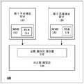
컴퓨팅 디바이스 (100) 는 제 1 프로세싱 유닛 (110), 제 2 프로세싱 유닛 (120) 및 시스템 메모리 (130) 를 포함한다. 제 1 프로세싱 유닛 (110) 은 MMU (112) 를 포함하고, 제 2 프로세싱 유닛 (120) 은 MMU (122) 를 포함한다. MMU (110) 는 TLB (114) 를 포함할 수도 있고, MMU (122) 는 TLB (124) 를 포함할 수도 있다. 제 1 프로세싱 유닛 (110) 은, 예를 들어, 디바이스 (100) 의 CPU 일 수도 있다. 제 2 프로세싱 유닛 (120) 은, 예를 들어, 디스플레이 상의 프리젠테이션을 위한 그랙픽스 데이터를 출력하도록 동작가능한 GPU 일 수도 있다. 제 1 프로세싱 유닛 (110) 및 제 2 프로세싱 유닛 (120) 은 부가적으로 디스플레이 제어기들, 네트워킹 디바이스들을 포함하는 다양한 주변 디바이스들을 위한 프로세싱 유닛들과 같은 프로세싱 유닛들의 다른 유형들, 또는 CPU 또는 GPU 와 같은 프로세서로부터 신호 프로세싱을 오프로드하는 디지털 신호 프로세싱 (DSP) 코어의 임의의 유형을 나타낼 수도 있다. 제 1 프로세싱 유닛 (110) 및 제 2 프로세싱 유닛 (120) 의 예들은, 디지털 신호 프로세서 (DSP), 범용 마이크로프로세서, 주문형 집적 회로 (ASIC), 필드 프로그램가능 로직 어레이 (FPGA), 또는 다른 등가의 집적 또는 이산 로직 회로를 포함할 수도 있지만, 이에 한정되지 않는다. 본 개시물의 기법들이 일반적으로 2 개의 프로세싱 유닛들을 참조하여 기재될 것이지만, 그 기법들은 2 개 초과의 프로세싱 유닛들로 구현될 수도 있다.The
시스템 메모리 (130) 는 컴퓨터 판독가능 저장 매체의 일 예일 수도 있다. 시스템 메모리는, 예를 들어 랜덤 액세스 메모리 (RAM) 의 일 유형, 예컨대 동적 RAM, 정적 RAM, 싸이리스터 RAM, 제로-캐패시터 RAM, 트윈 트랜지스터 RAM, 또는 휘발성 메모리의 일부 다른 유형일 수도 있다. 시스템 메모리 (130) 는 또한 비휘발성 메모리, 예컨대 플래시 메모리 또는 비휘발성 RAM 의 다른 유형일 수도 있다. 시스템 메모리 (130) 는 프로세싱 유닛 (110) 및 프로세싱 유닛 (120) 으로 하여금 본 개시물에서 각각에 대해 주어진 기능들을 수행하게 하는 명령들을 저장할 수도 있다. 이러한 식으로, 시스템 메모리 (130) 는 하나 이상의 프로세서들, 예를 들어 프로세싱 유닛 (110) 및 프로세싱 유닛 (120) 으로 하여금 다양한 기능들을 수행하게 하는 명령들을 포함하는 컴퓨터 판독가능 저장 매체로서 고려될 수도 있다. 하지만, 일부 예들에서, 그러한 명령들은 시스템 메모리 (130) 이외의 메모리 (도 1 에 도시되지 않음) 에 저장될 수도 있다.The
제 1 프로세싱 유닛 (110) 및 제 2 프로세싱 유닛 (120) 은 시스템 메모리 (130) 로부터 데이터를 판독하고 시스템 메모리 (130) 에 데이터를 기록하도록 구성된다. 데이터를 기록 또는 판독하기 위해, 제 1 프로세싱 유닛 (110) 및 제 2 프로세싱 유닛 (120) 은 시스템 메모리 (130) 에서의 특정 물리 위치들에 액세스하도록 구성된다. 이러한 특정 위치들은, 예를 들어, 4KB 의 청크들일 수도 있으며, 각각의 청크는 그 자신의 고유 물리 어드레스를 가질 수도 있다. 하지만, 위에서 도입된 바와 같이, 제 1 프로세싱 유닛 (110) 및 제 2 프로세싱 유닛 (120) 은 가상 어드레싱을 구현할 수도 있어서, 제 1 프로세싱 유닛 (110) 또는 제 2 프로세싱 유닛 (120) 상에서 실행하는 어플리케이션들이 인접 가상 메모리 어드레스들에 할당되도록 한다. 하지만, 이러한 인접 가상 메모리 어드레스들에 대응하는 물리 메모리 어드레스들은 단편화되며 비인접일 수도 있다. 따라서, 프로세싱 유닛 (110) 및 프로세싱 유닛 (120) 은 대응 비인접 물리 메모리 어드레스들 보다 오히려 이러한 인접 가상 메모리 어드레스들을 사용하여 데이터를 프로세싱할 수도 있다. 하지만, 프로세싱 유닛 (110) 및 프로세싱 유닛 (120) 이 시스템 메모리 (130) 에 액세스 (시스템 메모리 (130) 로부터 판독하거나 시스템 메모리 (130) 에 기록) 할 필요가 있을 때, 이러한 가상 메모리 어드레스들이 물리 메모리 어드레스들로 변환되어야 한다.The first processing unit 110 and the
MMU (112) 는 제 1 프로세싱 유닛 (110) 에 대해 가상 메모리 어드레스들을 물리 메모리 어드레스들로 맵핑하도록 구성되고, MMU (122) 는 제 2 프로세싱 유닛 (120) 에 대해 가상 메모리 어드레스들을 물리 메모리 어드레스들로 맵핑하도록 구성된다. 페이지 엔트리들의 전체 세트를 갖는 완전한 페이지 테이블이 공통 페이지 테이블 (132) 에 저장된다. TLB (114) 및 TLB (124) 의 각각은 공통 페이지 테이블 (132) 에 저장된 페이지 엔트리들의 서브세트를 저장한다. 서브세트는, 예를 들어, 최근에 액세스된 페이지 엔트리들, 빈번하게 액세스된 페이지 엔트리들, 또는 일부 다른 기준에 기초하여 선택된 페이지 엔트리들일 수도 있다. TLB (114) 에 저장된 페이지 엔트리들의 서브세트는 TLB (124) 에 저장된 페이지 엔트리들의 서브세트와 상이할 수도 있다. 예를 들어, MMU (112) 를 통해 제 1 프로세싱 유닛 (110) 에 의해 최근에 액세스된 또는 빈번하게 액세스된 페이지 테이블 엔트리들은 MMU (122) 를 통해 제 2 프로세싱 유닛 (120) 에 의해 최근에 또는 빈번하게 액세스된 페이지 테이블 엔트리들과 상이할 수도 있다. 따라서, TLB (114) 는 TLB (124) 와 상이한 페이지 테이블 엔트리들의 서브세트를 저장할 수도 있다.
예를 들어, 제 1 프로세싱 유닛 (110) 이 가상 메모리 어드레스를 물리 메모리 어드레스로 변환할 필요가 있으면, TLB (114) 가 그 가상 메모리 어드레스에 대한 페이지 엔트리를 저장할 때, MMU (112) 는 특정 가상 메모리 어드레스에 대응하는 물리 메모리 어드레스를 결정하기 위해 TLB (114) 를 사용할 수도 있다. 결정된 물리 메모리 어드레스를 사용하여, 프로세싱 유닛 (110) 은 시스템 메모리 (130) 의 특정 물리 위치로부터 판독하거나 그 특정 물리 위치에 기록할 수도 있다. 유사하게, 제 2 프로세싱 유닛 (120) 이 가상 메모리 어드레스를 물리 메모리 어드레스로 변환할 필요가 있으면, TLB (124) 가 그 가상 메모리 어드레스에 대한 페이지 엔트리를 저장할 때, MMU (122) 는 특정 가상 메모리 어드레스에 대응하는 물리 메모리 어드레스를 결정하기 위해 TLB (124) 를 사용할 수도 있다. 결정된 물리 메모리 어드레스를 사용하여, 프로세싱 유닛 (120) 은 시스템 메모리 (130) 로부터 판독하거나 시스템 메모리 (130) 에 기록할 수도 있다.For example, when the first processing unit 110 needs to convert a virtual memory address to a physical memory address, when the
위에서 도입된 바와 같이, TLB (114) 및 TLB (124) 는 단지 가상 메모리 어드레스들의 서브세트에 대해서만 가상-투-물리 맵핑들을 저장하는 캐시들일 수도 있다. 따라서, TLB (114) 는 프로세싱 유닛 (110) 에 대한 가상-투-물리 맵핑 전체를 저장하지 않을 수도 있으며, 유사하게 TLB (124) 는 프로세싱 유닛 (120) 에 대한 가상-투-물리 맵핑 전체를 저장하지 않을 수도 있다. 일부 경우들에서, MMU (112) 는 TLB (114) 에 저장된 맵핑을 갖지 않는 가상 메모리 어드레스들에 대한 대응 물리 메모리 어드레스들을 결정할 필요가 있을 수도 있다. TLB (114) 에 포함되지 않는 가상 메모리 어드레스에 대한 맵핑을 결정하기 위해, 제 1 프로세싱 유닛 (110) 은 시스템 메모리 (130) 에 저장된 공통 페이지 테이블 (132) 에 액세스할 수도 있다. 공통 페이지 테이블 (132) 은 프로세싱 유닛 (110) 에 대한 가상-투-물리 맵핑 전체를 포함하며, 이에 따라 TLB (114) 및 TLB (124) 보다 훨씬 클 수도 있다.As introduced above,
MMU (112) 와 마찬가지로, 일부 경우들에서, MMU (122) 는 TLB (124) 에 저장된 맵핑을 갖지 않는 가상 메모리 어드레스에 대한 대응 물리 메모리 어드레스를 결정할 필요가 있을 수도 있다. TLB (124) 에 포함되지 않은 가상 메모리 어드레스에 대한 맵핑을 결정하기 위해, 제 2 프로세싱 유닛 (120) 은 시스템 메모리 (130) 에 저장된 공통 페이지 테이블 (132) 에 액세스한다. 이러한 방식으로, MMU (122) 는 MMU (112) 와 실질적으로 유사한 방식으로 기능할 수도 있다. 공통 페이지 테이블 (132) 은 프로세싱 유닛 (110) 뿐만 아니라 프로세싱 유닛 (120) 에 대한 가상-투-물리 맵핑 전체를 포함한다. 이러한 방식으로, 제 1 프로세싱 유닛 (110) 및 제 2 프로세싱 유닛 (120) 은 동일한 페이지 테이블 (즉, 도 1 의 예에서 공통 페이지 테이블 (132)) 을 공유한다. 프로세싱 유닛 (110) 및 프로세싱 유닛 (120) 에 의해 공유된 공통 페이지 테이블은, MMU (112) 및 MMU (122) 가 프로세싱 유닛 (110) 및 프로세싱 유닛 (120) 에 대한 별도의 페이지 테이블들을 유지하고 있었다면, 2 개의 페이지 테이블들의 결합된 사이즈보다 작을 수도 있다. 공통 페이지 테이블 (132) 은 2 개의 별도의 페이지 테이블들의 결합된 사이즈보다 작을 수도 있는데, 이는 공통 페이지 테이블 (132) 의 페이지 테이블 엔트리들의 일부가 MMU (112) 및 MMU (122) 의 양자에 의해 공유되기 때문이다.As with the
공통 페이지 테이블 (132) 은 가상 메모리 어드레스를 메모리 청크의 물리 메모리 어드레스로 맵핑하는 복수의 페이지 엔트리들을 포함할 수도 있다. 메모리 청크는 그 물리 메모리 어드레스를 통해 개별적으로 액세스가능한 시스템 메모리 (130) 의 부분일 수도 있다. 각각의 페이지 엔트리는 속성 비트들의 제 1 세트 및 속성 비트들의 제 2 세트를 포함할 수도 있다. 속성 비트들의 제 1 세트는, 제 1 프로세싱 유닛 (110) 에 대한, 승인 및 액세스 권한과 같은 제어들을 설정할 수도 있고, 속성 비트들의 제 2 세트는 제 2 프로세싱 유닛 (120) 에 대한 제어들을 설정한다. 각각의 페이지 엔트리는 옵션으로 속성 비트들의 하나 이상의 부가 세트들, 예컨대 제 1 프로세싱 유닛 (110) 및 제 2 프로세싱 유닛 (120) 의 양자에 대한 공통 제어들을 설정하는 속성 비트들의 세트를 포함할 수도 있다.The common page table 132 may include a plurality of page entries that map the virtual memory address to the physical memory address of the memory chunk. The memory chunk may be part of the
공통 페이지 테이블 (132) 의 페이지 엔트리들에 대한 속성 비트들의 제 1 세트 및 속성 비트들의 제 2 세트는 제 1 프로세싱 유닛 (110) 및 제 2 프로세싱 유닛 (120) 이 공통 페이지 테이블을 공유하면서 상이한 승인 및 액세스 권한을 갖는 것을 가능하게 한다. 일 예로서, 속성 비트들의 제 1 세트는, 제 1 프로세싱 유닛 (110) 이 시스템 메모리 (130) 의 특정 메모리 청크에 대한 판독 및 기록 액세스 모두를 갖고, 제 2 프로세싱 유닛 (120) 이 단지 동일한 특정 메모리 청크로의 판독 액세스만을 가질 수 있도록 설정될 수도 있다. 물론, 제 2 프로세싱 유닛 (120) 이 판독 및 기록 액세스 모두를 갖고, 제 1 프로세싱 유닛 (110) 은 단지 판독 액세스만을 갖거나, 제 1 프로세싱 유닛 (110) 및 제 2 프로세싱 유닛 (120) 중 하나는 판독 및 기록 액세스 모두를 갖고, 다른 하나는 판독 액세스 뿐만 아니라 기록 액세스도 갖지 않는, 다른 구성들이 또한 가능하다.The first set of attribute bits and the second set of attribute bits for the page entries in the common page table 132 are used to indicate that the first processing unit 110 and the
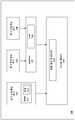
도 2 는 본 개시물의 기법들을 구현할 수도 있는, 다른 예의 컴퓨팅 디바이스인, 컴퓨팅 디바이스 (200) 를 나타낸다. 컴퓨팅 디바이스 (200) 의 예들은, 모바일 무선 전화기들, 개인용 디지털 보조기들 (PDAs), 비디오 게이밍 콘솔들, 핸드헬드 게이밍 유닛들, 모바일 화상 회의 유닛들, 랩탑 컴퓨터들, 데스크탑 컴퓨터들, 텔레비젼 셋톱 박스들, 디지털 미디어 플레이어들, 스마트폰들, 테블릿 컴퓨터들 등을 포함하지만 이에 한정되지 않는다. 컴퓨팅 디바이스 (200) 는 제 1 프로세싱 유닛 (210), 제 2 프로세싱 유닛 (220), 제 3 프로세싱 유닛 (240), 입력/출력 메모리 관리 유닛 (IOMMU)(222), 및 시스템 메모리 (230) 를 포함한다. 제 1 프로세싱 유닛 (210) 은 MMU (212) 를 포함한다. 제 2 프로세싱 유닛 (220) 및 제 3 프로세싱 유닛 (240) 은 각각 전용 MMU 를 갖지 않지만 대신 공통 MMU (즉, 도 2 에서의 IOMMU (222)) 를 갖는다. 제 1 프로세싱 유닛 (210) 은, 예를 들어 디바이스 (200) 의 CPU 일 수도 있다. 제 2 프로세싱 유닛 (120) 은, 예를 들어 디스플레이 상의 프리젠테이션을 위한 그래픽스 데이터를 출력하도록 동작가능한 GPU 일 수도 있다. 제 3 프로세싱 유닛 (240) 은, 예를 들어 주변 디바이스를 위한 프로세싱 유닛과 같은 프로세싱 유닛의 제 3 유형일 수도 있다. 제 1 프로세싱 유닛 (210), 제 2 프로세싱 유닛 (220) 및 제 3 프로세싱 유닛 (240) 의 예들은, 디지털 신호 프로세서 (DSP), 범용 마이크로프로세서, 주문형 집적 회로 (ASIC), 필드 프로그램가능 로직 어레이 (FPGA), 또는 다른 등가의 집적 또는 이산 로직 회로를 포함하지만, 이에 한정되지 않는다.FIG. 2 illustrates a
시스템 메모리 (230) 는 컴퓨터 판독가능 저장 매체의 일 예일 수도 있다. 시스템 메모리 (230) 는, 예를 들어, 랜덤 액세스 메모리 (RAM) 의 일 유형, 예컨대 동적 RAM, 정적 RAM, 싸이리스터 RAM, 제로-캐패시터 RAM, 트윈 트랜지스터 RAM, 또는 휘발성 메모리의 일부 다른 유형일 수도 있다. 시스템 메모리 (230) 는 또한 비휘발성 메모리, 예컨대 플래시 메모리 또는 비휘발성 RAM 의 다른 유형일 수도 있다. 시스템 메모리 (230) 는 프로세싱 유닛 (210) 및 프로세싱 유닛 (220) 으로 하여금 본 개시물에서 각각에 대해 주어진 기능들을 수행하게 하는 명령들을 저장할 수도 있다. 이러한 식으로, 시스템 메모리 (230) 는 하나 이상의 프로세서들, 예를 들어 프로세싱 유닛 (210), 프로세싱 유닛 (220), 및/또는 프로세싱 유닛 (240) 으로 하여금 다양한 기능들을 수행하게 하는 명령들을 포함하는 컴퓨터 판독가능 저장 매체로서 고려될 수도 있다. 하지만, 일부 예들에서, 그러한 명령들은 시스템 메모리 (230) 이외의 메모리 (도 2 에 도시되지 않음) 에 저장될 수도 있다.The
제 1 프로세싱 유닛 (210), 제 2 프로세싱 유닛 (220), 및 제 3 프로세싱 유닛 (240) 은 시스템 메모리 (230) 로부터 데이터를 판독하고 시스템 메모리 (230) 에 데이터를 기록하도록 구성된다. 데이터를 기록 또는 판독하기 위해, 제 1 프로세싱 유닛 (210), 제 2 프로세싱 유닛 (220) 및 제 3 프로세싱 유닛 (240) 은 시스템 메모리 (230) 에서의 특정 물리 위치들에 액세스하도록 구성된다. 이러한 특정 위치들은, 예를 들어, 4KB 의 청크들일 수도 있으며, 각각의 청크는 그 자신의 고유 물리 어드레스를 가질 수도 있다. 하지만, 위에서 도입된 바와 같이, 제 1 프로세싱 유닛 (210), 제 2 프로세싱 유닛 (220) 및 제 3 프로세싱 유닛 (240) 은 가상 어드레싱을 구현할 수도 있어서, 제 1 프로세싱 유닛 (210), 제 2 프로세싱 유닛 (220), 및/또는 제 3 프로세싱 유닛 (240) 상에서 실행하는 어플리케이션들의 작업들이 인접 가상 메모리 어드레스들에 할당되도록 한다. 하지만, 이러한 인접 가상 메모리 어드레스들에 대응하는 물리 메모리 어드레스들은 해체되며 비인접일 수도 있다. 따라서, 프로세싱 유닛 (210), 프로세싱 유닛 (220) 및 제 3 프로세싱 유닛 (240) 은 대응 비인접 물리 메모리 어드레스들 보다 오히려 이러한 인접 가상 메모리 어드레스들을 사용하여 데이터를 프로세싱할 수도 있다. 하지만, 프로세싱 유닛 (210), 프로세싱 유닛 (220) 및 프로세싱 유닛 (240) 이 시스템 메모리 (230) 에 액세스 (즉, 시스템 메모리 (230) 로부터 판독하거나 시스템 메모리 (230) 에 기록) 할 필요가 있을 때, 이러한 가상 메모리 어드레스들이 물리 메모리 어드레스들로 변환되어야 한다.The
MMU (212) 는 제 1 프로세싱 유닛 (210) 에 대해 가상 메모리 어드레스들을 물리 메모리 어드레스들로 맵핑하도록 구성된다. IOMMU (222) 는 제 2 프로세싱 유닛 (220) 및 제 3 프로세싱 유닛 (230) 양자에 대해 가상 메모리 어드레스들을 물리 메모리 어드레스들로 맵핑하도록 구성된다. 페이지 엔트리들의 전체 세트를 갖는 완전한 페이지 테이블이 공통 페이지 테이블 (232) 에 저장된다. TLB (214) 및 TLB (224) 의 각각은 공통 페이지 테이블 (232) 에 저장된 페이지 엔트리들의 서브세트를 저장한다. 서브세트는, 예를 들어, 최근에 액세스된 페이지 엔트리들, 빈번하게 액세스된 페이지 엔트리들, 또는 일부 다른 기준에 기초하여 선택된 페이지 엔트리들일 수도 있다.The
예를 들어, 제 1 프로세싱 유닛 (210) 이 가상 메모리 어드레스를 물리 메모리 어드레스로 변환할 필요가 있으면, TLB (214) 가 그 가상 메모리 어드레스에 대한 페이지 엔트리를 저장할 때, MMU (212) 는 특정 가상 메모리 어드레스에 대응하는 물리 메모리 어드레스를 결정하기 위해 TLB (214) 를 사용할 수도 있다. 결정된 물리 메모리 어드레스를 사용하여, 프로세싱 유닛 (210) 은 시스템 메모리 (230) 로부터 판독하거나 시스템 메모리 (230) 에 기록할 수도 있다. 유사하게, 제 2 프로세싱 유닛 (220) 또는 제 3 프로세싱 유닛 (240) 이 가상 메모리 어드레스를 물리 메모리 어드레스로 변환할 필요가 있으면, TLB (224) 가 그 가상 메모리 어드레스에 대한 페이지 엔트리를 저장할 때, MMU (222) 는 특정 가상 메모리 어드레스에 대응하는 물리 메모리 어드레스를 결정하기 위해 TLB (224) 를 사용할 수도 있다. 결정된 물리 메모리 어드레스를 사용하여, 제 2 프로세싱 유닛 (220) 및 제 3 프로세싱 유닛 (240) 은 시스템 메모리 (230) 로부터 판독하거나 시스템 메모리 (230) 에 기록할 수도 있다.For example, when the
위에서 도입된 바와 같이, TLB (214) 및 TLB (224) 는 단지 가상 메모리 어드레스들의 서브세트에 대해서만 가상-투-물리 맵핑들을 저장하는 캐시들일 수도 있다. 따라서, TLB (214) 는 제 1 프로세싱 유닛 (210) 에 대한 가상-투-물리 맵핑 전체를 저장하지 않을 수도 있으며, 유사하게 TLB (224) 는 제 2 프로세싱 유닛 (220) 및 제 3 프로세싱 유닛 (240) 에 대한 가상-투-물리 맵핑 전체를 저장하지 않을 수도 있다. 일부 경우들에서, MMU (212) 가 TLB (214) 에 저장된 맵핑을 갖지 않는 가상 메모리 어드레스들에 대한 대응 물리 메모리 어드레스를 결정할 필요가 있을 수도 있다. TLB (214) 에 포함되지 않는 가상 메모리 어드레스에 대한 맵핑을 결정하기 위해, MMU (212) 는 시스템 메모리 (230) 에 저장된 공통 페이지 테이블 (232) 에 액세스할 수도 있다. 공통 페이지 테이블 (232) 은 프로세싱 유닛 (210) 에 대한 가상-투-물리 맵핑 전체를 포함하며, 이에 따라 TLB (214) 보다 훨씬 클 수도 있다.As introduced above,
제 1 프로세싱 유닛 (210) 과 마찬가지로, 일부 경우들에서, 제 2 프로세싱 유닛 (220) 은 TLB (224) 에 저장된 맵핑을 갖지 않는 가상 메모리 어드레스에 대한 대응 물리 메모리 어드레스를 결정할 필요가 있을 수도 있다. TLB (224) 에 포함되지 않은 가상 메모리 어드레스에 대한 맵핑을 결정하기 위해, MMU (222) 는 시스템 메모리 (230) 에 저장된 공통 페이지 테이블 (232) 에 액세스한다. 공통 페이지 테이블 (232) 은 제 1 프로세싱 유닛 (210) 뿐만 아니라 제 2 프로세싱 유닛 (220) 및 제 3 프로세싱 유닛 (240) 에 대한 가상-투-물리 맵핑 전체를 포함한다. 이러한 방식으로, 제 1 프로세싱 유닛 (210), 제 2 프로세싱 유닛 (220) 및 제 3 프로세싱 유닛 (240) 은 동일한 페이지 테이블 (즉, 도 2 의 예에서 공통 페이지 테이블 (232)) 을 공유한다.As in the
공통 페이지 테이블 (232) 은 가상 메모리 어드레스를 메모리 청크의 물리 메모리 어드레스로 맵핑하는 복수의 페이지 엔트리들을 포함할 수도 있다. 각각의 페이지 엔트리는 속성 비트들의 제 1 세트 및 속성 비트들의 제 2 세트를 포함할 수도 있다. 속성 비트들의 제 1 세트는, 제 1 프로세싱 유닛 (210) 에 대한, 승인 및 액세스 권한과 같은 제어들을 설정할 수도 있고, 속성 비트들의 제 2 세트는 제 2 프로세싱 유닛 (220) 및 제 3 프로세싱 유닛 (240) 에 대한 제어들을 설정한다. 각각의 페이지 엔트리는 옵션으로 속성 비트들의 하나 이상의 부가 세트들, 예컨대 제 1 프로세싱 유닛 (210), 제 2 프로세싱 유닛 (220) 및 제 3 프로세싱 유닛 (240) 모두에 대한 공통 제어들을 설정하는 속성 비트들의 세트를 포함할 수도 있다.The common page table 232 may include a plurality of page entries that map the virtual memory address to the physical memory address of the memory chunk. Each page entry may comprise a first set of attribute bits and a second set of attribute bits. The first set of attribute bits may set controls such as grant and access rights for the
일부 예들에서, 속성 비트들의 제 2 세트는 IOMMU (222) 를 공유하는 모든 프로세싱 유닛들에 대한 제어들을 설정할 수도 있다. 따라서, 그러한 예에서, 속성 비트들의 제 2 세트는 제 2 프로세싱 유닛 (220) 및 제 3 프로세싱 유닛 (240) 양자에 대한 제어들을 정의한다. 하지만, 다른 예들에서, 제 2 프로세싱 유닛 (220) 및 제 3 프로세싱 유닛 (240) 은 각각 속성 비트들의 전용 세트를 가질 수도 있다. 그러한 예에서, 속성 비트들의 제 2 세트는 제 2 프로세싱 유닛 (220) 에 대한 제어들을 설정할 수도 있고, 속성 비트들의 제 3 세트는 제 3 프로세싱 유닛 (240) 에 대한 제어들을 설정할 수도 있다.In some instances, a second set of attribute bits may set controls for all processing units sharing the
공통 페이지 테이블 (232) 의 페이지 엔트리들에 대한 속성 비트들의 제 1 세트 및 속성 비트들의 제 2 세트는, 제 1 프로세싱 유닛 (210) 이 제 2 프로세싱 유닛 (220) 및 제 3 프로세싱 유닛 (240) 과 공통 페이지 테이블을 공유하면서 제 2 프로세싱 유닛 (220) 및 제 3 프로세싱 유닛 (240) 과 상이한 승인 및 액세스 권한을 갖는 것을 가능하게 한다. 일 예로서, 속성 비트들의 제 1 세트는, 제 1 프로세싱 유닛 (210) 이 시스템 메모리 (230) 의 특정 메모리 청크로의 판독 및 기록 액세스 모두를 갖고, 제 2 프로세싱 유닛 (220) 및 제 3 프로세싱 유닛 (240) 이 단지 동일한 특정 메모리 청크로의 판독 액세스만을 가질 수 있도록 설정될 수도 있다. 물론, 제 2 프로세싱 유닛 (220) 및 제 3 프로세싱 유닛 (240) 은 판독 및 기록 액세스 모두를 갖고, 제 1 프로세싱 유닛 (210) 이 단지 판독 액세스만을 갖거나, 제 2 프로세싱 유닛 (220) 및 제 3 프로세싱 유닛 (240) 은 판독 및 기록 액세스 모두를 갖고, 제 1 프로세싱 유닛 (210) 이 판독 액세스 뿐만 아니라 기록 액세스도 갖지 않는, 다른 구성들이 또한 가능하다.The first set of attribute bits and the second set of attribute bits for the page entries in the common page table 232 are set such that the
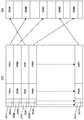
도 3 은 공통 페이지 테이블 (332) 의 양태들을 도시하는 개념적 다이어그램이다. 공통 페이지 테이블은 도 1 의 공통 페이지 테이블 (132) 또는 도 2 의 공통 페이지 테이블 (232) 중 어느 하나를 나타낼 수도 있다. 도 3 은 설명의 목적으로 개념적인 것으로 의도된 것이며, 실제 데이터 구조를 나타내는 것으로서 해석되지 않아야 한다. 공통 페이지 테이블 (332) 은 복수의 페이지 엔트리들을 포함한다. 각각의 페이지 엔트리는 속성 비트들의 제 1 세트 (352A-N), 속성 비트들의 제 2 세트 (354A-N), 속성 비트들의 제 3 세트 (356A-N), 및 물리 메모리 어드레스 비트들 (358A-N) 을 포함한다. 속성 비트들의 제 1 세트 (352A), 속성 비트들의 제 2 세트 (354A), 속성 비트들의 제 3 세트 (356A), 및 물리 메모리 어드레스 비트들 (358A) 은 페이지 엔트리 (A) 를 집합적으로 구성한다. 속성 비트들의 제 1 세트 (352B), 속성 비트들의 제 2 세트 (354B), 속성 비트들의 제 3 세트 (356B), 및 물리 메모리 어드레스 비트들 (358B) 은 페이지 엔트리 (B) 등을 집합적으로 구성한다. 위에서 논의된 바와 같이, 페이지 엔트리들 (356A-N) 의 각각은 32 비트, 40 비트 또는 일부 다른 사이즈일 수도 있다. 물리 메모리 어드레스 비트 (358A-N) 는 각각 20 비트 또는 일부 다른 사이즈일 수도 있으며, 다양한 사이즈들이 속성 비트들의 제 1 세트 (352A-N), 속성 비트들의 제 2 세트 (354A-N), 및 속성 비트들의 제 3 세트 (356A-N) 의 각각에 대해 사용될 수도 있다.FIG. 3 is a conceptual diagram illustrating aspects of the common page table 332. FIG. The common page table may represent either the common page table 132 of FIG. 1 or the common page table 232 of FIG. FIG. 3 is intended to be conceptual for the purposes of illustration and should not be construed as representing an actual data structure. The common page table 332 includes a plurality of page entries. Each page entry includes a first set of
도 3 에서 시스템 메모리 (334) 는 메모리 청크들 (134A-N) 을 갖는 물리 메모리를 나타낸다. 시스템 메모리 (334) 는 예를 들어 도 1 의 시스템 메모리 (130) 또는 도 2 의 시스템 메모리 (230) 에 대응할 수도 있다. 메모리 청크들 (134A-N) 은 메모리 (334) 의 비인접 청크들을 나타내기 위해 의도된 것이어서, 메모리 청크들 (334A-N) 의 물리 메모리 어드레스들이 비인접일 수도 있음을 의미한다. 페이지 엔트리들 (A-N) 의 각각은 물리 메모리 어드레스 비트들 (358A-N) 에서 메모리 청크들 (334A-N) 의 하나의 물리 어드레스를 포함한다.In FIG. 3,
페이지 엔트리들 (A-N) 의 각각은 가상 메모리 어드레스에 대응한다. 도 1 의 제 1 프로세싱 유닛 (110) 또는 제 2 프로세싱 유닛 (120) 과 같은 프로세싱 유닛이 시스템 메모리에 액세스할 필요가 있을 때, 가상 메모리 어드레스에 대한 대응 물리 메모리 어드레스를 찾기 위해 페이지 테이블 (332) 을 사용할 수 있다. 예를 들어, 제 1 프로세싱 유닛 (110) 이 특정 가상 메모리 어드레스를 물리 메모리 어드레스로 변환할 필요가 있으면, 제 1 프로세싱 유닛 (110) 은 그 특정 가상 메모리 어드레스에 대응하는 페이지 엔트리를 판독한다.Each of the page entries A-N corresponds to a virtual memory address. When a processing unit, such as the first processing unit 110 or the
본 예에서, 페이지 엔트리 (A) 가 특정 가상 메모리 어드레스에 대응한다고 가정한다. 따라서, 제 1 프로세싱 유닛 (110) 은 페이지 엔트리 (A) 를 판독하여 대응 물리 메모리 어드레스를 결정할 수도 있으며, 이는 물리 메모리 어드레스 비트들 (358A) 에 저장된다. 도 3 의 예에서, 엔트리 (A) 는 물리 메모리 청크 (334B) 가 저장되는 물리 메모리 어드레스로 맵핑한다. 따라서, 물리 메모리 어드레스 비트들 (358A) 은 메모리 청크 (334B) 가 위치되는 물리 어드레스를 시스템 메모리 (334) 내에 저장한다. 제 1 속성 비트들 (352A) 은 물리 메모리 청크 (334B) 에 액세스할 때 제 1 프로세싱 유닛 (110) 에 대한 승인들을 설정한다. 예를 들어, 제 1 비트는 제 1 프로세싱 유닛 (110) 이 메모리 청크 (334B) 에 대한 판독 특권들을 갖는지를 결정하였을 수도 있다. 제 2 비트는 제 1 프로세싱 유닛 (110) 이 메모리 청크 (334B) 에 대한 기록 특권들을 갖는지를 결정하였을 수도 있다.In this example, it is assumed that the page entry A corresponds to a specific virtual memory address. Thus, the first processing unit 110 may read page entry A to determine the corresponding physical memory address, which is stored in physical
일부 경우들에서, 제 2 프로세싱 유닛 (120) 은 제 1 프로세싱 유닛 (110) 에 의해 변환된 동일한 특정 가상 메모리 어드레스를 변환할 필요가 있을 수도 있다. 그렇게 하기 위해, 제 2 프로세싱 유닛 (120) 은 특정 가상 메모리 어드레스를 변환할 때 제 1 프로세싱 유닛 (110) 이 판독하는 그 특정 가상 메모리 어드레스에 대응하는 동일한 페이지 엔트리를 판독할 수도 있다.In some cases, the
본 예에서, 다시 페이지 엔트리 (A) 가 특정 가상 메모리 어드레스에 대응한다고 가정한다. 따라서, 제 2 프로세싱 유닛 (120) 은 페이지 엔트리 (A) 를 판독하여 대응 물리 메모리 어드레스를 결정할 수도 있으며, 이는 물리 메모리 비트들 (358A) 에 저장된다. 도 3 의 예에서, 엔트리 (A) 는 물리 메모리 청크 (334B) 로 맵핑한다. 이에 따라, 물리 메모리 어드레스 비트들 (358A) 은 메모리 청크 (334B) 의 물리 어드레스를 저장한다. 제 2 속성 비트들 (354A) 은 물리 메모리 청크 (334B) 에 액세스할 때 제 2 프로세싱 유닛 (120) 의 승인들을 정의한다. 예를 들어, 제 2 속성 비트들 (356A) 의 제 1 비트는 제 2 프로세싱 유닛 (120) 이 메모리 청크 (334B) 에 대한 판독 특권들을 갖는지를 결정하였을 수도 있다. 제 2 속성 비트들 (356A) 의 제 2 비트는 제 2 프로세싱 유닛 (120) 이 메모리 청크 (334B) 에 대한 기록 특권들을 갖는지를 결정하였을 수도 있다. 이러한 방식으로, 제 1 프로세싱 유닛 (110) 및 제 2 프로세싱 유닛 (120) 이 가상 메모리 어드레스를 물리 메모리 어드레스로 변환하기 위해 동일한 페이지 테이블에서의 동일한 페이지 엔트리에 액세싱하고 있더라도, 제 1 프로세싱 유닛 (110) 및 제 2 프로세싱 유닛 (120) 은 동일한 메모리 청크에 대한, 상이한 판독 및 기록 액세스와 같은 상이한 특권들을 가질 수도 있다.In this example, it is again assumed that the page entry A corresponds to a specific virtual memory address. Thus, the
다른 예에서, 도 2 의 제 1 프로세싱 유닛 (210), 또는 제 2 프로세싱 유닛 (220) 이나 제 3 프로세싱 유닛 (240) 중 하나와 같은 프로세싱 유닛은, 시스템 메모리에 액세스할 필요가 있을 때, 가상 메모리 어드레스에 대한 대응 물리 메모리 어드레스를 찾기 위해 페이지 테이블 (1332) 을 사용할 수 있다. 그러한 예에서, 제 1 속성 비트들 (352A-N) 은 제 1 프로세싱 유닛 (210) 에 대한 승인들을 정의할 수도 있고, 제 2 속성 비트들 (354A-N) 은 제 2 프로세싱 유닛 (220) 및 제 3 프로세싱 유닛 (240) 의 양자에 대한 승인들을 정의할 수도 있다. 이에 따라, 제 2 프로세싱 유닛 (220) 이 메모리 (334) 의 물리 메모리 청크에 액세스할 필요가 있을 때, 제 2 속성 비트들 (354A-N) 은 제 2 프로세싱 유닛 (220) 에 대한 승인들을 정의한다. 유사하게, 제 3 프로세싱 유닛 (240) 이 메모리 (334) 의 물리 메모리 청크에 액세스할 필요가 있을 때, 제 2 속성 비트들 (354A-N) 은 또한 제 3 프로세싱 유닛 (240) 에 대한 승인들을 정의한다.In another example, a processing unit, such as the
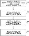
도 4 는 본 개시물에 기재하는 가상-투-물리 맵핑 기법들을 도시하는 플로우 다이어그램을 나타낸다. 도 4 의 기법들은 도 1 의 컴퓨팅 디바이스 (100) 또는 도 2 의 컴퓨팅 디바이스 (200) 와 같은, 2 이상의 프로세싱 유닛들을 갖는 컴퓨팅 디바이스에 의해 수행될 수 있다. 도 4 의 기법들은 컴퓨팅 디바이스 (100) 를 참조하여 기재될 것이지만, 도 4 의 기법들이 다수의 컴퓨팅 디바이스들에 적용가능하며 컴퓨팅 디바이스 (100) 로서 구성된 디바이스들에만 한정되는 것은 아니라는 것을 이해해야 한다.Figure 4 shows a flow diagram illustrating virtual-to-physical mapping techniques described in this disclosure. The techniques of FIG. 4 may be performed by a computing device having two or more processing units, such as
제 1 프로세싱 유닛 (110) 은 MMU (112) 를 통해 메모리에 저장된 공통 페이지 테이블을 사용하여 가상 메모리 어드레스를 물리 메모리 어드레스로 변환한다 (410). 공통 페이지 테이블은 제 1 프로세싱 유닛 (110) 및 제 2 프로세싱 유닛 (120) 에 공통이며, 어플리케이션에 의해 액세스된 메모리 청크들에 대한 물리 메모리 어드레스들로의 가상 메모리 어드레스들의 맵핑을 저장한다. 어플리케이션은 제 1 프로세싱 유닛 (110) 및 제 2 프로세싱 유닛 (120) 의 양자 상에서 실행될 수도 있다. 공통 페이지 테이블은 제 1 프로세싱 유닛 (110) 및 제 2 프로세싱 유닛 (120) 이 메모리 청크에 액세스하는데 사용하는 페이지 엔트리를 포함한다. 페이지 엔트리는 또한 메모리 청크의 물리 어드레스를 정의하는 물리 어드레스 비트들을 포함한다.The first processing unit 110 translates the virtual memory address to a physical memory address using the common page table stored in memory via the MMU 112 (410). The common page table is common to the first processing unit 110 and the
제 1 프로세싱 유닛 (120) 은 물리 메모리 어드레스에 의해 식별된 메모리 청크에 액세스한다 (420). 페이지 엔트리는 제 1 프로세싱 유닛에 의한 메모리 청크의 액세스가능성을 정의하는 속성 비트들의 제 1 세트를 포함한다. 제 2 프로세싱 유닛 (120) 은 메모리에 저장된 공통 페이지 테이블을 사용하여 가상 메모리 어드레스를 물리 메모리 어드레스로 변환한다 (430). 이러한 방식으로, 제 1 프로세싱 유닛 (110) 및 제 2 프로세싱 유닛 (120) 은, 가상 메모리 어드레스를 물리 메모리 어드레스로 변환할 때, 동일한 공통 페이지 테이블에 액세스한다. 제 2 프로세싱 유닛 (120) 은 물리 메모리 어드레스에 의해 식별된 메모리 청크에 액세스한다 (440). 페이지 엔트리는 제 2 프로세싱 유닛에 의한 동일한 메모리 청크의 액세스가능성을 정의하는 속성 비트들의 제 2 세트를 포함한다. 본 예에서, 제 1 프로세싱 유닛 (110) 및 제 2 프로세싱 유닛 (120) 은, 특정 가상 메모리 어드레스를 물리 메모리 어드레스로 변환할 때, 동일한 페이지 엔트리에 액세스하지만, 페이지 엔트리는 제 1 프로세싱 유닛 (110) 및 제 2 프로세싱 유닛 (120) 에 대한 별도의 속성 비트들을 가질 수 있다. 페이지 엔트리는 또한 제 1 프로세싱 유닛 (110) 및 제 2 프로세싱 유닛 (120) 의 양자에 공통인 속성들을 정의하는 속성 비트들의 제 3 세트를 포함할 수도 있다.The
도 4 의 예에서, 제 1 프로세싱 유닛 (110) 은 CPU 일 수도 있고, 제 2 프로세싱 유닛 (120) 은 GPU 일 수도 있다. 속성 비트들의 제 1 세트는 제 1 프로세싱 유닛 (110) 이 메모리 청크로의 기록 액세스를 갖는지를 정의할 수도 있고, 제 1 프로세싱 유닛 (110) 이 메모리 청크로의 판독 액세스를 갖는지를 정의할 수도 있다. 속성 비트들의 제 2 세트는 제 2 프로세싱 유닛 (120) 이 메모리 청크로의 기록 액세스를 갖는지를 정의할 수도 있고, 제 2 프로세싱 유닛 (120) 이 메모리 청크로의 판독 액세스를 갖는지를 정의할 수도 있다. 제 1 프로세싱 유닛 (110) 에 의한 메모리 청크의 액세스가능성은 제 2 프로세싱 유닛 (120) 에 의한 메모리 청크의 액세스가능성과 상이할 수도 있다. 예를 들어, 속성들의 제 1 세트에 기초하여, 제 1 프로세싱 유닛 (110) 은 메모리 청크로의 판독 액세스 및 기록 액세스를 가질 수도 있고, 속성들의 제 2 세트에 기초하여 제 2 프로세싱 유닛 (120) 은 메모리 청크로의 판독 액세스만을 갖는다.In the example of FIG. 4, the first processing unit 110 may be a CPU, and the
제 1 프로세싱 유닛 (110) 은 제 1 MMU (예를 들어, MMU (112)) 를 포함할 수도 있고, 제 2 프로세싱 유닛 (120) 은 제 2 MMU (예를 들어, MMU (122)) 를 포함할 수도 있다. 제 1 MMU 는 공통 페이지 테이블에 액세스하도록 구성될 수도 있고, 제 2 MMU 는 또한 동일한 공통 페이지 테이블에 액세스하도록 구성될 수도 있다.The first processing unit 110 may include a first MMU (e.g., MMU 112) and the
시스템 메모리 (26) 의 예들은, 랜덤 액세스 메모리 (RAM), 판독 전용 메모리 (ROM), 전기적 소거가능 프로그램가능 판독 전용 메모리 (EEPROM), CD-ROM, 또는 다른 광학 디스크 스토리지, 자기 디스크 스토리지, 또는 다른 자기 저장 디바이스, 플래시 메모리, 또는 컴퓨터 또는 프로세서에 의해 액세스될 수 있는 데이터 구조들 또는 명령들의 형태로 원하는 프로그램 코드를 반송 또는 저장하기 위해 사용될 수 있는 임의의 다른 매체를 포함하지만, 이에 한정되지 않는다. 시스템 메모리 (26) 는 일부 예들에서, 비일시적 저장 매체로서 고려될 수도 있다. 용어 "비일시적" 은 저장 매체가 반송파 또는 전파된 신호에서 구현되지 않는 것을 나타낼 수도 있다. 하지만, 용어 "비일시적" 은 시스템 메모리 (26) 가 비가동성인 것을 의미하도록 해석되지 않아야 한다. 일 예로서, 시스템 메모리 (26) 는 디바이스 (10) 로 부터 제거되고, 또 다른 디바이스로 이동될 수도 있다. 또 다른 예로서, 실질적으로 시스템 메모리 (26) 와 유사한 저장 디바이스가 디바이스 (10) 내에 삽입될 수도 있다. 소정의 예들에서, 비일시적 저장 매체는, 시간에 걸쳐 변화할 수 있는 데이터를 (예를 들어, RAM 에) 저장할 수도 있다.Examples of system memory 26 include random access memory (RAM), read only memory (ROM), electrically erasable programmable read only memory (EEPROM), CD-ROM or other optical disk storage, But is not limited to, any other magnetic storage device, flash memory, or any other medium that can be used to carry or store desired program code in the form of data structures or instructions that can be accessed by a computer or processor . The system memory 26 may, in some instances, be considered as a non-volatile storage medium. The term "non-transient" may indicate that the storage medium is not implemented in a carrier wave or propagated signal. However, the term "non-transient" should not be construed to mean that system memory 26 is inactive. As an example, the system memory 26 may be removed from the device 10 and moved to another device. As another example, a storage device substantially similar to the system memory 26 may be inserted into the device 10. In certain instances, the non-volatile storage medium may store data (e.g., in RAM) that may vary over time.
하나 이상의 예들에서, 기재된 기능들은 하드웨어, 소프트웨어, 펌웨어, 또는 이들의 임의의 조합으로 구현될 수도 있다. 소프트웨어로 구현되는 경우, 그 기능들은 컴퓨터 판독가능 매체 상에 하나 이상의 명령들 또는 코드로서 저장되거나 또는 그 매체 상으로 송신될 수도 있고, 하드웨어 기반 프로세싱 유닛에 의해 실행될 수도 있다. 컴퓨터 판독가능 매체는 예를 들어 통신 프로토콜에 따라, 하나의 장소로부터 다른 장소로의 컴퓨터 프로그램의 전송을 용이하게 하는 임의의 매체를 포함하는 유형의 매체, 예컨대 데이터 저장 매체, 또는 통신 매체에 대응하는, 컴퓨터 판독가능 저장 매체를 포함할 수도 있다. 이러한 방식으로, 컴퓨터 판독가능 매체는 일반적으로 (1) 비일시적인, 유형의 컴퓨터 판독가능 저장 매체, 또는 (2) 신호 또는 반송파와 같은, 통신 매체에 대응할 수도 있다. 데이터 저장 매체는 본 개시물에 기재된 기법들의 구현을 위한 명령들, 코드 및/또는 데이터 구조들을 취출하기 위해 하나 이상의 컴퓨터들 또는 하나 이상의 프로세서들에 의해 액세스될 수 있는 임의의 가용 매체들일 수도 있다. 컴퓨터 프로그램 제품은 컴퓨터 판독가능 매체를 포함할 수도 있다.In one or more examples, the functions described may be implemented in hardware, software, firmware, or any combination thereof. When implemented in software, the functions may be stored on or transmitted over as one or more instructions or code on a computer-readable medium, or may be executed by a hardware-based processing unit. The computer-readable medium may be any type of medium, such as a data storage medium, or a communication medium, including any medium that facilitates the transfer of a computer program from one place to another, for example, in accordance with a communication protocol , Computer-readable storage media. In this manner, the computer readable medium may generally correspond to (1) a non-transitory, type of computer readable storage medium, or (2) a communication medium, such as a signal or a carrier wave. The data storage medium may be one or more computers or any available media that can be accessed by one or more processors to retrieve instructions, code, and / or data structures for implementation of the techniques described in this disclosure. The computer program product may comprise a computer readable medium.
한정이 아닌 일 예로서, 그러한 컴퓨터 판독가능 매체들은 RAM, ROM, EEPROM, CD-ROM 또는 다른 광 디스크 저장, 자기 디스크 저장, 또는 다른 자기 저장 디바이스들, 플래시 메모리, 또는 원하는 프로그램 코드를 명령들 또는 데이터 구조들의 형태로 전달하거나 또는 저장하는데 이용될 수 있고 컴퓨터에 의해 액세스될 수 있는 임의의 다른 매체를 포함할 수 있다. 또한, 임의의 접속이 컴퓨터 판독가능 매체로 적절히 지칭된다. 예를 들어, 명령들은 동축 케이블, 광섬유 케이블, 트위스티드 페어, 디지털 가입자 회선 (DSL), 또는 적외선, 라디오, 및 마이크로파와 같은 무선 기술들을 이용하여 웹사이트, 서버, 또는 다른 원격 소스로부터 송신된다면, 동축 케이블, 광섬유 케이블, 트위스티드 페어, DSL, 또는 적외선, 라디오, 및 마이크로파와 같은 무선 기술들이 매체의 정의에 포함된다. 하지만, 컴퓨터 판독가능 저장 매체 및 데이터 저장 매체가 접속들, 반송파들, 신호들 또는 다른 일시적인 매체를 포함하는 것이 아니라 대신 비일시적인, 유형의 저장 매체로 지향된다는 것을 이해해야 한다. 디스크 (disk) 및 디스크 (disc) 는, 본 명세서에서 사용한 바와 같이, 컴팩트 디스크 (CD), 레이저 디스크, 광학 디스크, 디지털 다기능 디스크 (DVD), 플로피 디스크 및 블루-레이 디스크를 포함하며, 여기서 디스크 (disk) 들은 보통 데이터를 자기적으로 재생시키는 한편 디스크 (disc) 들은 레이저를 이용하여 데이터를 광학적으로 재생시킨다. 위의 조합들이 또한 컴퓨터 판독가능 매체들의 범위 내에 포함되어야 한다.By way of example, and not limitation, such computer-readable media may comprise RAM, ROM, EEPROM, CD-ROM or other optical disk storage, magnetic disk storage, or other magnetic storage devices, flash memory, Or any other medium that can be used to transfer or store data in the form of data structures and which can be accessed by a computer. Also, any connection is properly referred to as a computer-readable medium. For example, the instructions may be transmitted from a web site, server, or other remote source using wireless technologies such as coaxial cable, fiber optic cable, twisted pair, digital subscriber line (DSL), or infrared, radio, Wireless technologies such as cable, fiber optic cable, twisted pair, DSL, or infrared, radio, and microwave are included in the definition of media. However, it should be understood that the computer-readable storage medium and the data storage medium do not include connections, carriers, signals or other temporary media, but are instead directed to non-transitory, type of storage medium. A disk and a disc, as used herein, include a compact disc (CD), a laser disc, an optical disc, a digital versatile disc (DVD), a floppy disc and a Blu-ray disc, (discs) usually reproduce data magnetically, while discs use a laser to optically reproduce data. Combinations of the above should also be included within the scope of computer readable media.
명령들은 하나 이상의 프로세서들, 예컨대 하나 이상의 디지털 신호 프로세서들 (DSPs), 범용 마이크로프로세서들, 주문형 집적회로들 (ASICs), 필드 프로그램가능 로직 어레이들 (FPGAs), 또는 다른 등가의 집적 또는 이산 로직 회로와 같은, 하나 이상의 프로세서들에 의해 실행될 수도 있다. 따라서, 용어 “프로세서" 는, 본 명세서에서 사용한 바와 같이, 전술한 구조 또는 본 명세서에 기재된 기법들의 구현에 적합한 임의의 다른 구조 중 어느 것을 지칭할 수도 있다. 게다가, 일부 양태들에서, 본 명세서에 기재된 기능성은 인코딩 및 디코딩을 위해 구성되는 전용 하드웨어 및/또는 소프트웨어 모듈들 내에 제공되거나, 또는 결합된 코덱에 통합될 수도 있다. 또한, 이 기법들은 하나 이상의 회로들 또는 로직 엘리먼트들에서 전부 구현될 수 있다.The instructions may be executed by one or more processors, such as one or more digital signal processors (DSPs), general purpose microprocessors, application specific integrated circuits (ASICs), field programmable logic arrays (FPGAs), or other equivalent integrated or discrete logic circuits , ≪ / RTI > Thus, the term " processor ", as used herein, may refer to any of the structures described above or any other structure suitable for implementation of the techniques described herein. In addition, in some aspects, The described functionality may be provided in dedicated hardware and / or software modules that are configured for encoding and decoding, or may be incorporated into a combined codec. These techniques may also be implemented entirely in one or more circuits or logic elements have.
본 개시물의 기법들은 무선 핸드셋, 집적 회로 (IC) 또는 IC들의 세트 (예컨대, 칩 세트) 를 포함한, 매우 다양한 디바이스들 또는 장치들로 구현될 수도 있다. 여러 컴포넌트들, 모듈들, 또는 유닛들이 개시된 기법들을 수행하도록 구성된 디바이스들의 기능적 양태들을 강조하기 위해서 본 개시물에 기재되지만, 상이한 하드웨어 유닛들에 의한 실현을 반드시 필요로 하지는 않는다. 더 정확히 말하면, 위에서 기재된 바와 같이, 여러 유닛들이 코덱 하드웨어 유닛에 결합되거나 또는 적합한 소프트웨어 및/또는 펌웨어와 함께 위에서 설명한 바와 같은 하나 이상의 프로세서들을 포함한, 상호작용하는 하드웨어 유닛들의 컬렉션에 의해 제공될 수도 있다.The techniques of the present disclosure may be implemented in a wide variety of devices or devices, including a wireless handset, an integrated circuit (IC) or a set of ICs (e.g., a chip set). Although several components, modules, or units are described in this disclosure to emphasize functional aspects of devices configured to perform the disclosed techniques, implementation by different hardware units is not necessarily required. More precisely, as described above, several units may be coupled to a codec hardware unit or provided by a collection of interacting hardware units, including one or more processors as described above with appropriate software and / or firmware .
여러 예들이 기술되었다. 이들 및 다른 예들은 다음 청구항들의 범위 내에 있다.Several examples have been described. These and other examples are within the scope of the following claims.
Claims (36)
Translated fromKorean제 2 프로세싱 유닛; 및
메모리를 포함하고,
상기 메모리는,
상기 제 1 프로세싱 유닛 및 상기 제 2 프로세싱 유닛에 공통이고, 어플리케이션의 작업 (job) 에 의해 액세스된, 상기 메모리 내의 메모리 청크 (chunk) 들에 대한 물리 메모리 어드레스들로의 가상 메모리 어드레스들 맵핑을 저장하는 공통 페이지 테이블, 및
상기 제 1 프로세싱 유닛 및 상기 제 2 프로세싱 유닛이 상기 메모리 청크들의 메모리 청크에 액세스하는데 사용하는, 상기 공통 페이지 테이블 내의 페이지 엔트리를 저장하며,
상기 페이지 엔트리는 상기 제 1 프로세싱 유닛에 의한 상기 메모리 청크의 액세스가능성을 정의하는 속성 비트들의 제 1 세트, 상기 제 2 프로세싱 유닛에 의한 동일한 메모리 청크의 액세스가능성을 정의하는 속성 비트들의 제 2 세트, 및 상기 메모리 내의 상기 메모리 청크의 물리 어드레스를 정의하는 물리 어드레스 비트들을 포함하는, 장치.A first processing unit;
A second processing unit; And
Memory,
The memory comprising:
Store virtual memory address mappings to physical memory addresses for memory chunks in the memory common to the first processing unit and the second processing unit and accessed by a job of the application A common page table, and
Store a page entry in the common page table that the first processing unit and the second processing unit use to access memory chunks of the memory chunks,
The page entry comprising a first set of attribute bits defining accessibility of the memory chunk by the first processing unit, a second set of attribute bits defining accessibility of the same memory chunk by the second processing unit, And physical address bits defining a physical address of the memory chunk in the memory.
상기 페이지 엔트리는 상기 제 1 프로세싱 유닛 및 상기 제 2 프로세싱 유닛 양자에 공통인 속성들을 정의하는 속성 비트들의 제 3 세트를 포함하는, 장치.The method according to claim 1,
Wherein the page entry comprises a third set of attribute bits defining attributes common to both the first processing unit and the second processing unit.
상기 제 1 프로세싱 유닛은 중앙 프로세싱 유닛 (CPU) 를 포함하고, 상기 제 2 프로세싱 유닛은 그래픽스 프로세싱 유닛 (GPU) 을 포함하는, 장치.The method according to claim 1,
Wherein the first processing unit comprises a central processing unit (CPU) and the second processing unit comprises a graphics processing unit (GPU).
상기 속성 비트들의 제 1 세트는, 상기 제 1 프로세싱 유닛이 상기 메모리 청크로의 기록 액세스를 갖는지를 정의하고, 그리고 상기 제 1 프로세싱 유닛이 상기 메모리 청크로의 판독 액세스를 갖는지를 정의하며,
상기 속성 비트들의 제 2 세트는, 상기 제 2 프로세싱 유닛이 상기 메모리 청크로의 기록 액세스를 갖는지를 정의하고, 그리고 상기 제 2 프로세싱 유닛이 상기 메모리 청크로의 판독 액세스를 갖는지를 정의하는, 장치.The method according to claim 1,
Wherein the first set of attribute bits defines whether the first processing unit has write access to the memory chunk and defines whether the first processing unit has read access to the memory chunk,
Wherein the second set of attribute bits define whether the second processing unit has write access to the memory chunk and that the second processing unit has read access to the memory chunk.
상기 제 1 프로세싱 유닛에 의한 상기 메모리 청크의 액세스가능성은 상기 제 2 프로세싱 유닛에 의한 상기 메모리 청크의 액세스가능성과 상이한, 장치.The method according to claim 1,
Wherein the accessibility of the memory chunk by the first processing unit is different from the accessibility of the memory chunk by the second processing unit.
상기 속성 비트들의 제 1 세트는, 상기 제 1 프로세싱 유닛이 상기 메모리 청크로의 판독 액세스 및 기록 액세스를 갖는 것을 정의하고,
상기 속성 비트들의 제 2 세트는, 상기 제 2 프로세싱 유닛이 상기 메모리 청크로의 판독 전용 액세스를 갖는 것을 정의하는, 장치.The method according to claim 1,
The first set of attribute bits defining that the first processing unit has read access and write access to the memory chunk,
Wherein the second set of attribute bits define that the second processing unit has read-only access to the memory chunk.
상기 제 1 프로세싱 유닛은 제 1 메모리 관리 유닛 (MMU) 을 포함하고, 상기 제 2 프로세싱 유닛은 제 2 MMU 를 포함하며,
상기 제 1 MMU 는 상기 공통 페이지 테이블에 액세스하도록 구성되고, 상기 제 2 MMU 는 상기 공통 페이지 테이블에 액세스하도록 구성되는, 장치.The method according to claim 1,
Wherein the first processing unit comprises a first memory management unit (MMU), the second processing unit comprises a second MMU,
Wherein the first MMU is configured to access the common page table and the second MMU is configured to access the common page table.
제 1 메모리 관리 유닛 (MMU) 으로서, 상기 제 1 프로세싱 유닛이 상기 제 1 MMU 를 포함하는, 상기 제 1 MMU;
제 3 프로세싱 유닛;
입력/출력 MMU (IOMMU) 로서, 상기 제 2 프로세싱 유닛 및 상기 제 3 프로세싱 유닛에 의해 공유되는, 상기 IOMMU 를 더 포함하고,
상기 제 1 MMU 는 상기 공통 페이지 테이블에 액세스하도록 구성되고, 상기 IOMMU 는 상기 공통 페이지 테이블에 액세스하도록 구성되는, 장치.The method according to claim 1,
A first memory management unit (MMU), wherein the first processing unit comprises the first MMU;
A third processing unit;
Further comprising an I / O MMU (IOMMU), the IOMMU being shared by the second processing unit and the third processing unit,
Wherein the first MMU is configured to access the common page table and the IOMMU is configured to access the common page table.
상기 어플리케이션은 상기 제 1 프로세싱 유닛 및 상기 제 2 프로세싱 유닛의 양자 상에서 실행하는, 장치.The method according to claim 1,
The application executing on both the first processing unit and the second processing unit.
상기 제 1 프로세싱 유닛에 의해, 상기 물리 메모리 어드레스에 의해 식별된 메모리 청크에 액세스하는 단계;
제 2 프로세싱 유닛에 의해, 상기 메모리에 저장된 상기 공통 페이지 테이블을 사용하여 상기 가상 메모리 어드레스를 상기 물리 메모리 어드레스로 변환하는 단계; 및
상기 제 2 프로세싱 유닛에 의해, 상기 물리 메모리 어드레스에 의해 식별된 상기 메모리 청크에 액세스하는 단계를 포함하고,
상기 공통 페이지 테이블은 상기 제 1 프로세싱 유닛 및 상기 제 2 프로세싱 유닛에 공통이고, 어플리케이션의 작업에 의해 액세스된 메모리 청크들에 대한 물리 메모리 어드레스들로의 가상 메모리 어드레스들 맵핑을 저장하고,
상기 공통 페이지 테이블은 상기 제 1 프로세싱 유닛 및 상기 제 2 프로세싱 유닛이 상기 메모리 청크에 액세스하는데 사용하는 페이지 엔트리를 포함하며,
상기 페이지 엔트리는 상기 제 1 프로세싱 유닛에 의한 상기 메모리 청크의 액세스가능성을 정의하는 속성 비트들의 제 1 세트, 상기 제 2 프로세싱 유닛에 의한 동일한 메모리 청크의 액세스가능성을 정의하는 속성 비트들의 제 2 세트, 및 상기 메모리 청크의 물리 어드레스를 정의하는 물리 어드레스 비트들을 포함하는, 방법.Converting, by the first processing unit, a virtual memory address into a physical memory address using a common page table stored in the memory;
Accessing, by the first processing unit, a memory chunk identified by the physical memory address;
Converting, by the second processing unit, the virtual memory address into the physical memory address using the common page table stored in the memory; And
Accessing the memory chunk identified by the physical memory address by the second processing unit,
Wherein the common page table stores virtual memory address mappings to physical memory addresses for memory chunks common to the first processing unit and the second processing unit and accessed by operation of an application,
Wherein the common page table includes a page entry that the first processing unit and the second processing unit use to access the memory chunk,
The page entry comprising a first set of attribute bits defining accessibility of the memory chunk by the first processing unit, a second set of attribute bits defining accessibility of the same memory chunk by the second processing unit, And physical address bits defining a physical address of the memory chunk.
상기 페이지 엔트리는 상기 제 1 프로세싱 유닛 및 상기 제 2 프로세싱 유닛 양자에 공통인 속성들을 정의하는 속성 비트들의 제 3 세트를 포함하는, 방법.11. The method of claim 10,
Wherein the page entry comprises a third set of attribute bits defining attributes common to both the first processing unit and the second processing unit.
상기 제 1 프로세싱 유닛은 중앙 프로세싱 유닛 (CPU) 를 포함하고, 상기 제 2 프로세싱 유닛은 그래픽스 프로세싱 유닛 (GPU) 을 포함하는, 방법.11. The method of claim 10,
Wherein the first processing unit comprises a central processing unit (CPU) and the second processing unit comprises a graphics processing unit (GPU).
상기 속성 비트들의 제 1 세트는, 상기 제 1 프로세싱 유닛이 상기 메모리 청크로의 기록 액세스를 갖는지를 정의하고, 그리고 상기 제 1 프로세싱 유닛이 상기 메모리 청크로의 판독 액세스를 갖는지를 정의하며,
상기 속성 비트들의 제 2 세트는, 상기 제 2 프로세싱 유닛이 상기 메모리 청크로의 기록 액세스를 갖는지를 정의하고, 그리고 상기 제 2 프로세싱 유닛이 상기 메모리 청크로의 판독 액세스를 갖는지를 정의하는, 방법.11. The method of claim 10,
Wherein the first set of attribute bits defines whether the first processing unit has write access to the memory chunk and defines whether the first processing unit has read access to the memory chunk,
Wherein the second set of attribute bits define whether the second processing unit has write access to the memory chunk and that the second processing unit has read access to the memory chunk.
상기 제 1 프로세싱 유닛에 의한 상기 메모리 청크의 액세스가능성은 상기 제 2 프로세싱 유닛에 의한 상기 메모리 청크의 액세스가능성과 상이한, 방법.11. The method of claim 10,
Wherein the accessibility of the memory chunk by the first processing unit is different from the accessibility of the memory chunk by the second processing unit.
상기 속성 비트들의 제 1 세트에 기초하여, 상기 제 1 프로세싱 유닛이 상기 메모리 청크로의 판독 액세스 및 기록 액세스를 갖고,
상기 속성 비트들의 제 2 세트에 기초하여, 상기 제 2 프로세싱 유닛이 상기 메모리 청크로의 판독 전용 액세스를 갖는, 방법.11. The method of claim 10,
Wherein the first processing unit has read access and write access to the memory chunk based on the first set of attribute bits,
Wherein the second processing unit has a read-only access to the memory chunk based on the second set of attribute bits.
상기 제 1 프로세싱 유닛은 제 1 메모리 관리 유닛 (MMU) 을 포함하고, 상기 제 2 프로세싱 유닛은 제 2 MMU 를 포함하며,
상기 제 1 MMU 는 상기 공통 페이지 테이블에 액세스하도록 구성되고, 상기 제 2 MMU 는 상기 공통 페이지 테이블에 액세스하도록 구성되는, 방법.11. The method of claim 10,
Wherein the first processing unit comprises a first memory management unit (MMU), the second processing unit comprises a second MMU,
Wherein the first MMU is configured to access the common page table and the second MMU is configured to access the common page table.
제 3 프로세싱 유닛에 의해, 상기 메모리에 저장된 상기 공통 페이지 테이블을 사용하여 제 2 가상 메모리 어드레스를 제 2 물리 메모리 어드레스로 변환하는 단계; 및
상기 제 3 프로세싱 유닛에 의해, 상기 제 2 물리 메모리 어드레스에 의해 식별된 메모리 청크에 액세스하는 단계를 더 포함하고,
상기 제 2 프로세싱 유닛 및 상기 제 3 프로세싱 유닛은 입력/출력 MMU (IOMMU) 를 공유하고, 상기 IOMMU 는 상기 공통 페이지 테이블에 액세스하도록 구성되는, 방법.11. The method of claim 10,
Converting, by the third processing unit, the second virtual memory address into a second physical memory address using the common page table stored in the memory; And
Further comprising: by the third processing unit, accessing a memory chunk identified by the second physical memory address,
The second processing unit and the third processing unit share an input / output MMU (IOMMU), and the IOMMU is configured to access the common page table.
상기 어플리케이션은 상기 제 1 프로세싱 유닛 및 상기 제 2 프로세싱 유닛의 양자 상에서 실행하는, 방법.11. The method of claim 10,
The application executing on both the first processing unit and the second processing unit.
제 2 프로세싱 수단; 및
메모리를 포함하고,
상기 제 1 프로세싱 수단은,
상기 메모리에 저장된 공통 페이지 테이블을 사용하여 가상 메모리 어드레스를 물리 메모리 어드레스로 변환하기 위한 제 1 수단; 및
상기 물리 메모리 어드레스에 의해 식별된 메모리 청크에 액세스하기 위한 제 1 수단을 포함하고,
상기 제 2 프로세싱 수단은,
상기 메모리에 저장된 상기 공통 페이지 테이블을 사용하여 상기 가상 메모리 어드레스를 상기 물리 메모리 어드레스로 변환하기 위한 제 2 수단; 및
상기 물리 메모리 어드레스에 의해 식별된 상기 메모리 청크에 액세스하기 위한 제 2 수단을 포함하고,
상기 공통 페이지 테이블은 상기 제 1 프로세싱 수단 및 상기 제 2 프로세싱 수단에 공통이고, 어플리케이션의 작업에 의해 액세스된 메모리 청크들에 대한 물리 메모리 어드레스들로의 가상 메모리 어드레스들 맵핑을 저장하고,
상기 공통 페이지 테이블은 상기 제 1 프로세싱 수단 및 상기 제 2 프로세싱 수단이 상기 메모리 청크에 액세스하는데 사용하는 페이지 엔트리를 포함하며,
상기 페이지 엔트리는 상기 제 1 프로세싱 수단에 의한 상기 메모리 청크의 액세스가능성을 정의하는 속성 비트들의 제 1 세트, 상기 제 2 프로세싱 수단에 의한 동일한 메모리 청크의 액세스가능성을 정의하는 속성 비트들의 제 2 세트, 및 상기 메모리 청크의 물리 어드레스를 정의하는 물리 어드레스 비트들을 포함하는, 장치.First processing means;
Second processing means; And
Memory,
Wherein the first processing means comprises:
First means for converting a virtual memory address to a physical memory address using a common page table stored in the memory; And
And first means for accessing the memory chunk identified by the physical memory address,
Wherein the second processing means comprises:
Second means for converting the virtual memory address into the physical memory address using the common page table stored in the memory; And
And second means for accessing the memory chunk identified by the physical memory address,
Wherein the common page table stores virtual memory address mappings to physical memory addresses for memory chunks common to the first processing means and the second processing means and accessed by an operation of an application,
Wherein the common page table comprises a page entry that the first processing means and the second processing means use to access the memory chunk,
The page entry comprising a first set of attribute bits defining accessibility of the memory chunk by the first processing means, a second set of attribute bits defining accessibility of the same memory chunk by the second processing means, And physical address bits defining a physical address of the memory chunk.
상기 페이지 엔트리는 상기 제 1 프로세싱 수단 및 상기 제 2 프로세싱 수단 양자에 공통인 속성들을 정의하는 속성 비트들의 제 3 세트를 포함하는, 장치.20. The method of claim 19,
Wherein the page entry comprises a third set of attribute bits defining attributes common to both the first processing means and the second processing means.
상기 제 1 프로세싱 수단은 중앙 프로세싱 유닛 (CPU) 를 포함하고, 상기 제 2 프로세싱 수단은 그래픽스 프로세싱 유닛 (GPU) 을 포함하는, 장치.20. The method of claim 19,
Wherein the first processing means comprises a central processing unit (CPU) and the second processing means comprises a graphics processing unit (GPU).
상기 속성 비트들의 제 1 세트는, 상기 제 1 프로세싱 수단이 상기 메모리 청크로의 기록 액세스를 갖는지를 정의하고, 그리고 상기 제 1 프로세싱 수단이 상기 메모리 청크로의 판독 액세스를 갖는지를 정의하며,
상기 속성 비트들의 제 2 세트는, 상기 제 2 프로세싱 수단이 상기 메모리 청크로의 기록 액세스를 갖는지를 정의하고, 그리고 상기 제 2 프로세싱 수단이 상기 메모리 청크로의 판독 액세스를 갖는지를 정의하는, 장치.20. The method of claim 19,
Wherein the first set of attribute bits defines whether the first processing means has write access to the memory chunk and defines whether the first processing means has read access to the memory chunk,
Wherein the second set of attribute bits define whether the second processing means has write access to the memory chunk and that the second processing means has read access to the memory chunk.
상기 제 1 프로세싱 수단에 의한 상기 메모리 청크의 액세스가능성은 상기 제 2 프로세싱 수단에 의한 상기 메모리 청크의 액세스가능성과 상이한, 장치.20. The method of claim 19,
The accessibility of the memory chunk by the first processing means being different from the accessibility of the memory chunk by the second processing means.
상기 속성 비트들의 제 1 세트에 기초하여, 상기 제 1 프로세싱 수단이 상기 메모리 청크로의 판독 액세스 및 기록 액세스를 갖고,
상기 속성 비트들의 제 2 세트에 기초하여, 상기 제 2 프로세싱 수단이 상기 메모리 청크로의 판독 전용 액세스를 갖는, 장치.20. The method of claim 19,
Based on the first set of attribute bits, the first processing means having read access and write access to the memory chunk,
And wherein the second processing means has a read-only access to the memory chunk based on the second set of attribute bits.
상기 제 1 프로세싱 수단은 제 1 메모리 관리 유닛 (MMU) 을 포함하고, 상기 제 2 프로세싱 수단은 제 2 MMU 를 포함하며,
상기 제 1 MMU 는 상기 공통 페이지 테이블에 액세스하도록 구성되고, 상기 제 2 MMU 는 상기 공통 페이지 테이블에 액세스하도록 구성되는, 장치.20. The method of claim 19,
Wherein the first processing means comprises a first memory management unit (MMU) and the second processing means comprises a second MMU,
Wherein the first MMU is configured to access the common page table and the second MMU is configured to access the common page table.
제 3 프로세싱 수단을 더 포함하고,
상기 제 3 프로세싱 수단은,
상기 메모리에 저장된 상기 공통 페이지 테이블을 사용하여 제 2 가상 메모리 어드레스를 제 2 물리 메모리 어드레스로 변환하기 위한 제 2 수단; 및
상기 제 2 물리 메모리 어드레스에 의해 식별된 상기 메모리 청크에 액세스하기 위한 상기 제 2 수단을 포함하는, 장치.20. The method of claim 19,
Further comprising a third processing means,
Wherein the third processing means comprises:
Second means for converting a second virtual memory address to a second physical memory address using the common page table stored in the memory; And
And said second means for accessing said memory chunk identified by said second physical memory address.
상기 어플리케이션은 상기 제 1 프로세싱 수단 및 상기 제 2 프로세싱 수단의 양자 상에서 실행하는, 장치.20. The method of claim 19,
The application executing on both the first processing means and the second processing means.
상기 제 1 프로세싱 유닛에 의해, 메모리에 저장된 공통 페이지 테이블을 사용하여 가상 메모리 어드레스를 물리 메모리 어드레스로 변환하게 하고;
상기 제 1 프로세싱 유닛에 의해, 상기 물리 메모리 어드레스에 의해 식별된 메모리 청크에 액세스하게 하고;
상기 제 2 프로세싱 유닛에 의해, 상기 메모리에 저장된 상기 공통 페이지 테이블을 사용하여 상기 가상 메모리 어드레스를 상기 물리 메모리 어드레스로 변환하게 하고;
상기 제 2 프로세싱 유닛에 의해, 상기 물리 메모리 어드레스에 의해 식별된 상기 메모리 청크에 액세스하게 하는 명령들을 저장하며,
상기 공통 페이지 테이블은 상기 제 1 프로세싱 유닛 및 상기 제 2 프로세싱 유닛에 공통이고, 어플리케이션의 작업에 의해 액세스된 메모리 청크들에 대한 물리 메모리 어드레스들로의 가상 메모리 어드레스들 맵핑을 저장하고,
상기 공통 페이지 테이블은 상기 제 1 프로세싱 유닛 및 상기 제 2 프로세싱 유닛이 상기 메모리 청크에 액세스하는데 사용하는 페이지 엔트리를 포함하며,
상기 페이지 엔트리는 상기 제 1 프로세싱 유닛에 의한 상기 메모리 청크의 액세스가능성을 정의하는 속성 비트들의 제 1 세트, 상기 제 2 프로세싱 유닛에 의한 동일한 메모리 청크의 액세스가능성을 정의하는 속성 비트들의 제 2 세트, 및 상기 메모리 청크의 물리 어드레스를 정의하는 물리 어드레스 비트들을 포함하는, 컴퓨터 판독가능 저장 매체.When executed, the first processing unit and the second processing unit,
Cause the first processing unit to use the common page table stored in the memory to convert the virtual memory address to a physical memory address;
Access, by the first processing unit, the memory chunk identified by the physical memory address;
Cause the second processing unit to use the common page table stored in the memory to convert the virtual memory address into the physical memory address;
Store instructions for causing the second processing unit to access the memory chunk identified by the physical memory address,
Wherein the common page table stores virtual memory address mappings to physical memory addresses for memory chunks common to the first processing unit and the second processing unit and accessed by operation of an application,
Wherein the common page table includes a page entry that the first processing unit and the second processing unit use to access the memory chunk,
The page entry comprising a first set of attribute bits defining accessibility of the memory chunk by the first processing unit, a second set of attribute bits defining accessibility of the same memory chunk by the second processing unit, And physical address bits defining a physical address of the memory chunk.
상기 페이지 엔트리는 상기 제 1 프로세싱 유닛 및 상기 제 2 프로세싱 유닛 양자에 공통인 속성들을 정의하는 속성 비트들의 제 3 세트를 포함하는, 컴퓨터 판독가능 저장 매체.29. The method of claim 28,
Wherein the page entry comprises a third set of attribute bits defining attributes common to both the first processing unit and the second processing unit.
상기 제 1 프로세싱 유닛은 중앙 프로세싱 유닛 (CPU) 를 포함하고, 상기 제 2 프로세싱 유닛은 그래픽스 프로세싱 유닛 (GPU) 을 포함하는, 컴퓨터 판독가능 저장 매체.29. The method of claim 28,
Wherein the first processing unit comprises a central processing unit (CPU), and the second processing unit comprises a graphics processing unit (GPU).
상기 속성 비트들의 제 1 세트는, 상기 제 1 프로세싱 유닛이 상기 메모리 청크로의 기록 액세스를 갖는지를 정의하고, 그리고 상기 제 1 프로세싱 유닛이 상기 메모리 청크로의 판독 액세스를 갖는지를 정의하며,
상기 속성 비트들의 제 2 세트는, 상기 제 2 프로세싱 유닛이 상기 메모리 청크로의 기록 액세스를 갖는지를 정의하고, 그리고 상기 제 2 프로세싱 유닛이 상기 메모리 청크로의 판독 액세스를 갖는지를 정의하는, 컴퓨터 판독가능 저장 매체.29. The method of claim 28,
Wherein the first set of attribute bits defines whether the first processing unit has write access to the memory chunk and defines whether the first processing unit has read access to the memory chunk,
Wherein the second set of attribute bits defines whether the second processing unit has write access to the memory chunk and defines whether the second processing unit has read access to the memory chunk, Possible storage medium.
상기 제 1 프로세싱 유닛에 의한 상기 메모리 청크의 액세스가능성은 상기 제 2 프로세싱 유닛에 의한 상기 메모리 청크의 액세스가능성과 상이한, 컴퓨터 판독가능 저장 매체.29. The method of claim 28,
Wherein the accessibility of the memory chunk by the first processing unit is different from the accessibility of the memory chunk by the second processing unit.
상기 속성 비트들의 제 1 세트에 기초하여, 상기 제 1 프로세싱 유닛이 상기 메모리 청크로의 판독 액세스 및 기록 액세스를 갖고,
상기 속성 비트들의 제 2 세트에 기초하여, 상기 제 2 프로세싱 유닛이 상기 메모리 청크로의 판독 전용 액세스를 갖는, 컴퓨터 판독가능 저장 매체.29. The method of claim 28,
Wherein the first processing unit has read access and write access to the memory chunk based on the first set of attribute bits,
And wherein the second processing unit has a read-only access to the memory chunk based on the second set of attribute bits.
상기 제 1 프로세싱 유닛은 제 1 메모리 관리 유닛 (MMU) 을 포함하고, 상기 제 2 프로세싱 유닛은 제 2 MMU 를 포함하며,
상기 제 1 MMU 는 상기 공통 페이지 테이블에 액세스하도록 구성되고, 상기 제 2 MMU 는 상기 공통 페이지 테이블에 액세스하도록 구성되는, 컴퓨터 판독가능 저장 매체.29. The method of claim 28,
Wherein the first processing unit comprises a first memory management unit (MMU), the second processing unit comprises a second MMU,
Wherein the first MMU is configured to access the common page table and the second MMU is configured to access the common page table.
실행될 때, 제 3 프로세싱 유닛으로 하여금,
상기 제 3 프로세싱 유닛에 의해, 상기 메모리에 저장된 상기 공통 페이지 테이블을 사용하여 제 2 가상 메모리 어드레스를 제 2 물리 메모리 어드레스로 변환하게 하고,
상기 제 3 프로세싱 유닛에 의해, 상기 제 2 물리 메모리 어드레스에 의해 식별된 메모리 청크에 액세스하게 하는,
부가 명령들을 저장하며,
상기 제 2 프로세싱 유닛 및 상기 제 3 프로세싱 유닛은 입력/출력 MMU (IOMMU) 를 공유하고, 상기 IOMMU 는 상기 공통 페이지 테이블에 액세스하도록 구성되는, 컴퓨터 판독가능 저장 매체.29. The method of claim 28,
When executed, the third processing unit,
Cause the third processing unit to convert the second virtual memory address to a second physical memory address using the common page table stored in the memory,
And to cause the third processing unit to access the memory chunk identified by the second physical memory address,
Additional instructions,
Wherein the second processing unit and the third processing unit share an input / output MMU (IOMMU), and the IOMMU is configured to access the common page table.
상기 어플리케이션은 상기 제 1 프로세싱 유닛 및 상기 제 2 프로세싱 유닛의 양자 상에서 실행하는, 컴퓨터 판독가능 저장 매체.29. The method of claim 28,
The application executing on both the first processing unit and the second processing unit.
Applications Claiming Priority (3)
| Application Number | Priority Date | Filing Date | Title |
|---|---|---|---|
| US13/565,434 | 2012-08-02 | ||
| US13/565,434US8938602B2 (en) | 2012-08-02 | 2012-08-02 | Multiple sets of attribute fields within a single page table entry |
| PCT/US2013/051069WO2014022110A1 (en) | 2012-08-02 | 2013-07-18 | Multiple sets of attribute fields within a single page table entry |
Publications (2)
| Publication Number | Publication Date |
|---|---|
| KR20150038513Atrue KR20150038513A (en) | 2015-04-08 |
| KR102051698B1 KR102051698B1 (en) | 2019-12-03 |
Family
ID=48916200
Family Applications (1)
| Application Number | Title | Priority Date | Filing Date |
|---|---|---|---|
| KR1020157005315AActiveKR102051698B1 (en) | 2012-08-02 | 2013-07-18 | Multiple sets of attribute fields within a single page table entry |
Country Status (8)
| Country | Link |
|---|---|
| US (1) | US8938602B2 (en) |
| EP (1) | EP2880540B1 (en) |
| JP (3) | JP2015527661A (en) |
| KR (1) | KR102051698B1 (en) |
| BR (1) | BR112015001988B1 (en) |
| ES (1) | ES2763545T3 (en) |
| HU (1) | HUE047108T2 (en) |
| WO (1) | WO2014022110A1 (en) |
Cited By (1)
| Publication number | Priority date | Publication date | Assignee | Title |
|---|---|---|---|---|
| KR101942663B1 (en)* | 2017-09-28 | 2019-01-25 | 한국과학기술원 | Method and system to improve tlb coverage by using chunks of contiguous memory |
Families Citing this family (14)
| Publication number | Priority date | Publication date | Assignee | Title |
|---|---|---|---|---|
| US9141559B2 (en) | 2012-01-04 | 2015-09-22 | Intel Corporation | Increasing virtual-memory efficiencies |
| US9373182B2 (en) | 2012-08-17 | 2016-06-21 | Intel Corporation | Memory sharing via a unified memory architecture |
| US9378572B2 (en) | 2012-08-17 | 2016-06-28 | Intel Corporation | Shared virtual memory |
| US9436616B2 (en) | 2013-05-06 | 2016-09-06 | Qualcomm Incorporated | Multi-core page table sets of attribute fields |
| US20140331019A1 (en)* | 2013-05-06 | 2014-11-06 | Microsoft Corporation | Instruction set specific execution isolation |
| US9530000B2 (en)* | 2013-06-14 | 2016-12-27 | Microsoft Technology Licensing, Llc | Secure privilege level execution and access protection |
| US9563571B2 (en) | 2014-04-25 | 2017-02-07 | Apple Inc. | Intelligent GPU memory pre-fetching and GPU translation lookaside buffer management |
| US9507726B2 (en)* | 2014-04-25 | 2016-11-29 | Apple Inc. | GPU shared virtual memory working set management |
| US9921897B2 (en) | 2016-01-06 | 2018-03-20 | International Business Machines Corporation | Testing a non-core MMU |
| GB2547242B (en)* | 2016-02-11 | 2018-05-23 | Advanced Risc Mach Ltd | Graphics processing |
| US10019377B2 (en)* | 2016-05-23 | 2018-07-10 | Advanced Micro Devices, Inc. | Managing cache coherence using information in a page table |
| US10747679B1 (en)* | 2017-12-11 | 2020-08-18 | Amazon Technologies, Inc. | Indexing a memory region |
| CN110198331B (en)* | 2018-03-28 | 2022-11-25 | 腾讯科技(上海)有限公司 | A method and system for synchronizing data |
| CN112115521B (en)* | 2019-06-19 | 2023-02-07 | 华为技术有限公司 | Data access method and device |
Citations (1)
| Publication number | Priority date | Publication date | Assignee | Title |
|---|---|---|---|---|
| US20070168644A1 (en)* | 2006-01-17 | 2007-07-19 | Hummel Mark D | Using an IOMMU to Create Memory Archetypes |
Family Cites Families (15)
| Publication number | Priority date | Publication date | Assignee | Title |
|---|---|---|---|---|
| JP3454854B2 (en)* | 1992-01-16 | 2003-10-06 | 株式会社東芝 | Memory management device and method |
| US6446034B1 (en) | 1998-12-16 | 2002-09-03 | Bull Hn Information Systems Inc. | Processor emulation virtual memory address translation |
| US6286092B1 (en) | 1999-05-12 | 2001-09-04 | Ati International Srl | Paged based memory address translation table update method and apparatus |
| US7444636B2 (en) | 2002-07-15 | 2008-10-28 | Hewlett-Packard Development Company, L.P. | Method and system of determining attributes of a functional unit in a multiple processor computer system |
| US7111145B1 (en) | 2003-03-25 | 2006-09-19 | Vmware, Inc. | TLB miss fault handler and method for accessing multiple page tables |
| US7539842B2 (en) | 2006-08-15 | 2009-05-26 | International Business Machines Corporation | Computer memory system for selecting memory buses according to physical memory organization information stored in virtual address translation tables |
| US7865675B2 (en) | 2007-12-06 | 2011-01-04 | Arm Limited | Controlling cleaning of data values within a hardware accelerator |
| US8015361B2 (en) | 2007-12-14 | 2011-09-06 | International Business Machines Corporation | Memory-centric page table walker |
| US8099541B2 (en)* | 2008-01-22 | 2012-01-17 | Globalfoundries Inc. | Minivisor entry point in virtual machine monitor address space |
| US8397049B2 (en)* | 2009-07-13 | 2013-03-12 | Apple Inc. | TLB prefetching |
| US20110016290A1 (en) | 2009-07-14 | 2011-01-20 | Arie Chobotaro | Method and Apparatus for Supporting Address Translation in a Multiprocessor Virtual Machine Environment |
| US8386745B2 (en)* | 2009-07-24 | 2013-02-26 | Advanced Micro Devices, Inc. | I/O memory management unit including multilevel address translation for I/O and computation offload |
| US20110161620A1 (en) | 2009-12-29 | 2011-06-30 | Advanced Micro Devices, Inc. | Systems and methods implementing shared page tables for sharing memory resources managed by a main operating system with accelerator devices |
| US8669990B2 (en)* | 2009-12-31 | 2014-03-11 | Intel Corporation | Sharing resources between a CPU and GPU |
| US20120233439A1 (en) | 2011-03-11 | 2012-09-13 | Boris Ginzburg | Implementing TLB Synchronization for Systems with Shared Virtual Memory Between Processing Devices |
- 2012
- 2012-08-02USUS13/565,434patent/US8938602B2/enactiveActive
- 2013
- 2013-07-18BRBR112015001988-9Apatent/BR112015001988B1/enactiveIP Right Grant
- 2013-07-18JPJP2015525447Apatent/JP2015527661A/ennot_activeWithdrawn
- 2013-07-18EPEP13745243.9Apatent/EP2880540B1/enactiveActive
- 2013-07-18KRKR1020157005315Apatent/KR102051698B1/enactiveActive
- 2013-07-18WOPCT/US2013/051069patent/WO2014022110A1/enactiveApplication Filing
- 2013-07-18HUHUE13745243Apatent/HUE047108T2/enunknown
- 2013-07-18ESES13745243Tpatent/ES2763545T3/enactiveActive
- 2017
- 2017-10-19JPJP2017202603Apatent/JP2018041485A/ennot_activeWithdrawn
- 2019
- 2019-02-01JPJP2019016836Apatent/JP6728419B2/enactiveActive
Patent Citations (1)
| Publication number | Priority date | Publication date | Assignee | Title |
|---|---|---|---|---|
| US20070168644A1 (en)* | 2006-01-17 | 2007-07-19 | Hummel Mark D | Using an IOMMU to Create Memory Archetypes |
Cited By (1)
| Publication number | Priority date | Publication date | Assignee | Title |
|---|---|---|---|---|
| KR101942663B1 (en)* | 2017-09-28 | 2019-01-25 | 한국과학기술원 | Method and system to improve tlb coverage by using chunks of contiguous memory |
Also Published As
| Publication number | Publication date |
|---|---|
| BR112015001988A2 (en) | 2017-07-04 |
| BR112015001988B1 (en) | 2022-03-15 |
| KR102051698B1 (en) | 2019-12-03 |
| EP2880540A1 (en) | 2015-06-10 |
| JP2019109906A (en) | 2019-07-04 |
| JP2015527661A (en) | 2015-09-17 |
| US20140040593A1 (en) | 2014-02-06 |
| JP6728419B2 (en) | 2020-07-22 |
| EP2880540B1 (en) | 2019-09-25 |
| CN104508641A (en) | 2015-04-08 |
| ES2763545T3 (en) | 2020-05-29 |
| WO2014022110A1 (en) | 2014-02-06 |
| US8938602B2 (en) | 2015-01-20 |
| HUE047108T2 (en) | 2020-04-28 |
| JP2018041485A (en) | 2018-03-15 |
Similar Documents
| Publication | Publication Date | Title |
|---|---|---|
| KR102051698B1 (en) | Multiple sets of attribute fields within a single page table entry | |
| KR101708142B1 (en) | Multi-core page table sets of attribute fields | |
| JP4941148B2 (en) | Dedicated mechanism for page mapping in GPU | |
| US20170177497A1 (en) | Compressed caching of a logical-to-physical address table for nand-type flash memory | |
| US20140331019A1 (en) | Instruction set specific execution isolation | |
| US9146879B1 (en) | Virtual memory management for real-time embedded devices | |
| US20140310484A1 (en) | System and method for globally addressable gpu memory | |
| US20160188251A1 (en) | Techniques for Creating a Notion of Privileged Data Access in a Unified Virtual Memory System | |
| US8898429B2 (en) | Application processor and a computing system having the same | |
| US9367478B2 (en) | Controlling direct memory access page mappings | |
| CA3142618A1 (en) | Hardware-based memory compression | |
| US8347064B1 (en) | Memory access techniques in an aperture mapped memory space | |
| US8028118B2 (en) | Using an index value located on a page table to index page attributes | |
| US9916255B2 (en) | Data storage based on memory persistency | |
| US20160103766A1 (en) | Lookup of a data structure containing a mapping between a virtual address space and a physical address space | |
| US12380034B2 (en) | Extended attributes for shared page tables | |
| CN114461391A (en) | A remappable GPU main memory access management method and system |
Legal Events
| Date | Code | Title | Description |
|---|---|---|---|
| PA0105 | International application | Patent event date:20150227 Patent event code:PA01051R01D Comment text:International Patent Application | |
| PG1501 | Laying open of application | ||
| A201 | Request for examination | ||
| PA0201 | Request for examination | Patent event code:PA02012R01D Patent event date:20180702 Comment text:Request for Examination of Application | |
| E902 | Notification of reason for refusal | ||
| PE0902 | Notice of grounds for rejection | Comment text:Notification of reason for refusal Patent event date:20190719 Patent event code:PE09021S01D | |
| E701 | Decision to grant or registration of patent right | ||
| PE0701 | Decision of registration | Patent event code:PE07011S01D Comment text:Decision to Grant Registration Patent event date:20191030 | |
| GRNT | Written decision to grant | ||
| PR0701 | Registration of establishment | Comment text:Registration of Establishment Patent event date:20191127 Patent event code:PR07011E01D | |
| PR1002 | Payment of registration fee | Payment date:20191127 End annual number:3 Start annual number:1 | |
| PG1601 | Publication of registration | ||
| PR1001 | Payment of annual fee | Payment date:20220921 Start annual number:4 End annual number:4 | |
| PR1001 | Payment of annual fee | Payment date:20230921 Start annual number:5 End annual number:5 | |
| PR1001 | Payment of annual fee |