KR20150032427A - Thin film structure and method of fabricating the same - Google Patents
Thin film structure and method of fabricating the sameDownload PDFInfo
- Publication number
- KR20150032427A KR20150032427AKR20130111909AKR20130111909AKR20150032427AKR 20150032427 AKR20150032427 AKR 20150032427AKR 20130111909 AKR20130111909 AKR 20130111909AKR 20130111909 AKR20130111909 AKR 20130111909AKR 20150032427 AKR20150032427 AKR 20150032427A
- Authority
- KR
- South Korea
- Prior art keywords
- layer
- silicon
- sapphire
- gallium nitride
- support substrate
- Prior art date
- Legal status (The legal status is an assumption and is not a legal conclusion. Google has not performed a legal analysis and makes no representation as to the accuracy of the status listed.)
- Granted
Links
Images


Classifications
- H—ELECTRICITY
- H01—ELECTRIC ELEMENTS
- H01L—SEMICONDUCTOR DEVICES NOT COVERED BY CLASS H10
- H01L21/00—Processes or apparatus adapted for the manufacture or treatment of semiconductor or solid state devices or of parts thereof
- H01L21/02—Manufacture or treatment of semiconductor devices or of parts thereof
- H01L21/02104—Forming layers
- H01L21/02365—Forming inorganic semiconducting materials on a substrate
- H01L21/02436—Intermediate layers between substrates and deposited layers
- H01L21/02439—Materials
- C—CHEMISTRY; METALLURGY
- C30—CRYSTAL GROWTH
- C30B—SINGLE-CRYSTAL GROWTH; UNIDIRECTIONAL SOLIDIFICATION OF EUTECTIC MATERIAL OR UNIDIRECTIONAL DEMIXING OF EUTECTOID MATERIAL; REFINING BY ZONE-MELTING OF MATERIAL; PRODUCTION OF A HOMOGENEOUS POLYCRYSTALLINE MATERIAL WITH DEFINED STRUCTURE; SINGLE CRYSTALS OR HOMOGENEOUS POLYCRYSTALLINE MATERIAL WITH DEFINED STRUCTURE; AFTER-TREATMENT OF SINGLE CRYSTALS OR A HOMOGENEOUS POLYCRYSTALLINE MATERIAL WITH DEFINED STRUCTURE; APPARATUS THEREFOR
- C30B29/00—Single crystals or homogeneous polycrystalline material with defined structure characterised by the material or by their shape
- C30B29/10—Inorganic compounds or compositions
- C30B29/38—Nitrides
- C—CHEMISTRY; METALLURGY
- C23—COATING METALLIC MATERIAL; COATING MATERIAL WITH METALLIC MATERIAL; CHEMICAL SURFACE TREATMENT; DIFFUSION TREATMENT OF METALLIC MATERIAL; COATING BY VACUUM EVAPORATION, BY SPUTTERING, BY ION IMPLANTATION OR BY CHEMICAL VAPOUR DEPOSITION, IN GENERAL; INHIBITING CORROSION OF METALLIC MATERIAL OR INCRUSTATION IN GENERAL
- C23C—COATING METALLIC MATERIAL; COATING MATERIAL WITH METALLIC MATERIAL; SURFACE TREATMENT OF METALLIC MATERIAL BY DIFFUSION INTO THE SURFACE, BY CHEMICAL CONVERSION OR SUBSTITUTION; COATING BY VACUUM EVAPORATION, BY SPUTTERING, BY ION IMPLANTATION OR BY CHEMICAL VAPOUR DEPOSITION, IN GENERAL
- C23C14/00—Coating by vacuum evaporation, by sputtering or by ion implantation of the coating forming material
- C23C14/22—Coating by vacuum evaporation, by sputtering or by ion implantation of the coating forming material characterised by the process of coating
- C23C14/48—Ion implantation
- C—CHEMISTRY; METALLURGY
- C23—COATING METALLIC MATERIAL; COATING MATERIAL WITH METALLIC MATERIAL; CHEMICAL SURFACE TREATMENT; DIFFUSION TREATMENT OF METALLIC MATERIAL; COATING BY VACUUM EVAPORATION, BY SPUTTERING, BY ION IMPLANTATION OR BY CHEMICAL VAPOUR DEPOSITION, IN GENERAL; INHIBITING CORROSION OF METALLIC MATERIAL OR INCRUSTATION IN GENERAL
- C23C—COATING METALLIC MATERIAL; COATING MATERIAL WITH METALLIC MATERIAL; SURFACE TREATMENT OF METALLIC MATERIAL BY DIFFUSION INTO THE SURFACE, BY CHEMICAL CONVERSION OR SUBSTITUTION; COATING BY VACUUM EVAPORATION, BY SPUTTERING, BY ION IMPLANTATION OR BY CHEMICAL VAPOUR DEPOSITION, IN GENERAL
- C23C16/00—Chemical coating by decomposition of gaseous compounds, without leaving reaction products of surface material in the coating, i.e. chemical vapour deposition [CVD] processes
- C23C16/22—Chemical coating by decomposition of gaseous compounds, without leaving reaction products of surface material in the coating, i.e. chemical vapour deposition [CVD] processes characterised by the deposition of inorganic material, other than metallic material
- C23C16/30—Deposition of compounds, mixtures or solid solutions, e.g. borides, carbides, nitrides
- C23C16/34—Nitrides
- C—CHEMISTRY; METALLURGY
- C30—CRYSTAL GROWTH
- C30B—SINGLE-CRYSTAL GROWTH; UNIDIRECTIONAL SOLIDIFICATION OF EUTECTIC MATERIAL OR UNIDIRECTIONAL DEMIXING OF EUTECTOID MATERIAL; REFINING BY ZONE-MELTING OF MATERIAL; PRODUCTION OF A HOMOGENEOUS POLYCRYSTALLINE MATERIAL WITH DEFINED STRUCTURE; SINGLE CRYSTALS OR HOMOGENEOUS POLYCRYSTALLINE MATERIAL WITH DEFINED STRUCTURE; AFTER-TREATMENT OF SINGLE CRYSTALS OR A HOMOGENEOUS POLYCRYSTALLINE MATERIAL WITH DEFINED STRUCTURE; APPARATUS THEREFOR
- C30B25/00—Single-crystal growth by chemical reaction of reactive gases, e.g. chemical vapour-deposition growth
- C30B25/02—Epitaxial-layer growth
- C30B25/18—Epitaxial-layer growth characterised by the substrate
- C—CHEMISTRY; METALLURGY
- C30—CRYSTAL GROWTH
- C30B—SINGLE-CRYSTAL GROWTH; UNIDIRECTIONAL SOLIDIFICATION OF EUTECTIC MATERIAL OR UNIDIRECTIONAL DEMIXING OF EUTECTOID MATERIAL; REFINING BY ZONE-MELTING OF MATERIAL; PRODUCTION OF A HOMOGENEOUS POLYCRYSTALLINE MATERIAL WITH DEFINED STRUCTURE; SINGLE CRYSTALS OR HOMOGENEOUS POLYCRYSTALLINE MATERIAL WITH DEFINED STRUCTURE; AFTER-TREATMENT OF SINGLE CRYSTALS OR A HOMOGENEOUS POLYCRYSTALLINE MATERIAL WITH DEFINED STRUCTURE; APPARATUS THEREFOR
- C30B29/00—Single crystals or homogeneous polycrystalline material with defined structure characterised by the material or by their shape
- C30B29/10—Inorganic compounds or compositions
- C30B29/40—AIIIBV compounds wherein A is B, Al, Ga, In or Tl and B is N, P, As, Sb or Bi
- C30B29/403—AIII-nitrides
- C30B29/406—Gallium nitride
- H—ELECTRICITY
- H01—ELECTRIC ELEMENTS
- H01L—SEMICONDUCTOR DEVICES NOT COVERED BY CLASS H10
- H01L21/00—Processes or apparatus adapted for the manufacture or treatment of semiconductor or solid state devices or of parts thereof
- H01L21/02—Manufacture or treatment of semiconductor devices or of parts thereof
- H01L21/02104—Forming layers
- H01L21/02107—Forming insulating materials on a substrate
- H01L21/02109—Forming insulating materials on a substrate characterised by the type of layer, e.g. type of material, porous/non-porous, pre-cursors, mixtures or laminates
- H01L21/02112—Forming insulating materials on a substrate characterised by the type of layer, e.g. type of material, porous/non-porous, pre-cursors, mixtures or laminates characterised by the material of the layer
- H01L21/02123—Forming insulating materials on a substrate characterised by the type of layer, e.g. type of material, porous/non-porous, pre-cursors, mixtures or laminates characterised by the material of the layer the material containing silicon
- H01L21/02164—Forming insulating materials on a substrate characterised by the type of layer, e.g. type of material, porous/non-porous, pre-cursors, mixtures or laminates characterised by the material of the layer the material containing silicon the material being a silicon oxide, e.g. SiO2
- H—ELECTRICITY
- H01—ELECTRIC ELEMENTS
- H01L—SEMICONDUCTOR DEVICES NOT COVERED BY CLASS H10
- H01L21/00—Processes or apparatus adapted for the manufacture or treatment of semiconductor or solid state devices or of parts thereof
- H01L21/02—Manufacture or treatment of semiconductor devices or of parts thereof
- H01L21/02104—Forming layers
- H01L21/02365—Forming inorganic semiconducting materials on a substrate
- H01L21/02367—Substrates
- H01L21/0237—Materials
- H01L21/0242—Crystalline insulating materials
- H—ELECTRICITY
- H01—ELECTRIC ELEMENTS
- H01L—SEMICONDUCTOR DEVICES NOT COVERED BY CLASS H10
- H01L21/00—Processes or apparatus adapted for the manufacture or treatment of semiconductor or solid state devices or of parts thereof
- H01L21/02—Manufacture or treatment of semiconductor devices or of parts thereof
- H01L21/02104—Forming layers
- H01L21/02365—Forming inorganic semiconducting materials on a substrate
- H01L21/02436—Intermediate layers between substrates and deposited layers
- H01L21/02439—Materials
- H01L21/02441—Group 14 semiconducting materials
- H01L21/0245—Silicon, silicon germanium, germanium
- H—ELECTRICITY
- H01—ELECTRIC ELEMENTS
- H01L—SEMICONDUCTOR DEVICES NOT COVERED BY CLASS H10
- H01L21/00—Processes or apparatus adapted for the manufacture or treatment of semiconductor or solid state devices or of parts thereof
- H01L21/02—Manufacture or treatment of semiconductor devices or of parts thereof
- H01L21/02104—Forming layers
- H01L21/02365—Forming inorganic semiconducting materials on a substrate
- H01L21/02436—Intermediate layers between substrates and deposited layers
- H01L21/02439—Materials
- H01L21/02488—Insulating materials
- H—ELECTRICITY
- H01—ELECTRIC ELEMENTS
- H01L—SEMICONDUCTOR DEVICES NOT COVERED BY CLASS H10
- H01L21/00—Processes or apparatus adapted for the manufacture or treatment of semiconductor or solid state devices or of parts thereof
- H01L21/02—Manufacture or treatment of semiconductor devices or of parts thereof
- H01L21/02104—Forming layers
- H01L21/02365—Forming inorganic semiconducting materials on a substrate
- H01L21/02518—Deposited layers
- H01L21/02521—Materials
- H01L21/02538—Group 13/15 materials
- H01L21/0254—Nitrides
- H—ELECTRICITY
- H01—ELECTRIC ELEMENTS
- H01L—SEMICONDUCTOR DEVICES NOT COVERED BY CLASS H10
- H01L21/00—Processes or apparatus adapted for the manufacture or treatment of semiconductor or solid state devices or of parts thereof
- H01L21/02—Manufacture or treatment of semiconductor devices or of parts thereof
- H01L21/02104—Forming layers
- H01L21/02365—Forming inorganic semiconducting materials on a substrate
- H01L21/02656—Special treatments
- H01L21/02658—Pretreatments
- H—ELECTRICITY
- H10—SEMICONDUCTOR DEVICES; ELECTRIC SOLID-STATE DEVICES NOT OTHERWISE PROVIDED FOR
- H10D—INORGANIC ELECTRIC SEMICONDUCTOR DEVICES
- H10D62/00—Semiconductor bodies, or regions thereof, of devices having potential barriers
- H10D62/40—Crystalline structures
- H—ELECTRICITY
- H10—SEMICONDUCTOR DEVICES; ELECTRIC SOLID-STATE DEVICES NOT OTHERWISE PROVIDED FOR
- H10D—INORGANIC ELECTRIC SEMICONDUCTOR DEVICES
- H10D62/00—Semiconductor bodies, or regions thereof, of devices having potential barriers
- H10D62/80—Semiconductor bodies, or regions thereof, of devices having potential barriers characterised by the materials
- H10D62/85—Semiconductor bodies, or regions thereof, of devices having potential barriers characterised by the materials being Group III-V materials, e.g. GaAs
- H10D62/8503—Nitride Group III-V materials, e.g. AlN or GaN
Landscapes
- Engineering & Computer Science (AREA)
- Chemical & Material Sciences (AREA)
- Manufacturing & Machinery (AREA)
- Physics & Mathematics (AREA)
- Computer Hardware Design (AREA)
- Microelectronics & Electronic Packaging (AREA)
- Power Engineering (AREA)
- Condensed Matter Physics & Semiconductors (AREA)
- General Physics & Mathematics (AREA)
- Materials Engineering (AREA)
- Metallurgy (AREA)
- Organic Chemistry (AREA)
- Crystallography & Structural Chemistry (AREA)
- Inorganic Chemistry (AREA)
- Chemical Kinetics & Catalysis (AREA)
- General Chemical & Material Sciences (AREA)
- Mechanical Engineering (AREA)
- Recrystallisation Techniques (AREA)
Abstract
Translated fromKoreanDescription
Translated fromKorean본 발명은 박막 구조체 및 그 제조방법으로서, 보다 구체적으로는, 질화갈륨으로 구성된 에피층을 포함하는 박막 구조체 및 그 제조방법에 관한 것이다.The present invention relates to a thin film structure and a manufacturing method thereof, and more particularly to a thin film structure including an epitaxial layer composed of gallium nitride and a manufacturing method thereof.
고품질의 단결정 질화갈륨(GaN)의 성장은 고출력의 광전 소자 어플리케이션에 필수적이다. 벌크 갈륨에 대한 질소의 낮은 고용도 등에 기인하여 질화갈륨 기판은 질화갈륨의 호모에피택시 공정에서 상업적으로 유용하지 않다. 따라서, 질화갈륨계 소자 기판은, 사파이어 또는 탄화규소 등을 포함하는 다양한 이종 기판 상에 헤테로에피텍시에 의하여 성장된다. 상기 제안된 기판들 중에서 사파이어가 육방정계 대칭성과 질화갈륨 성장 공정에서 고온 안정성 등에 기인하여 가장 널리 사용되고 있다. 하지만, 사파이어와 질화갈륨 사이의 격자 부정합에 기인하여 발생된 관통 전위(threading dislocation)들과 적층결함들은 질화갈륨 에피층에 높은 결함 밀도를 유발한다. 이러한 결함 밀도를 감소시키기 위하여 과성장 래터럴 에피택시(ELOG)와 같은 래터럴 에피택시 공정이 제안되고 있으며, 이에 의하여 관통 전위의 밀도를 106cm-2이하로 감소시킬 수 있다. 그러나, 이러한 밀도값은 GaAs 호모에피택시에 대한 밀도값(102내지 104cm-2)보다 여전이 더 높은 실정이다.The growth of high quality single crystal gallium nitride (GaN) is essential for high power optoelectronic applications. Gallium nitride substrates are not commercially useful in the homoepitaxy process of gallium nitride due to the low solubility of nitrogen to bulk gallium and the like. Accordingly, the gallium nitride based substrate is grown by heteroepitaxy on various kinds of substrates including sapphire or silicon carbide. Among the above-mentioned substrates, sapphire is most widely used due to hexagonal symmetry and high-temperature stability in a gallium nitride growth process. However, threading dislocations and stacking faults caused by lattice mismatch between sapphire and gallium nitride cause high defect density in the gallium nitride epitaxial layer. These and this in order to reduce the defect density and lateral epitaxial growth process, such as lateral epitaxy (ELOG) is proposed, whereby the density of the
본 발명은 상기와 같은 문제점을 포함하여 여러 문제점들을 해결하기 위한 것으로서, 질화갈륨의 결함 밀도를 현저하게 감소시킬 수 있는 박막 구조체 및 그 제조방법을 제공하는 것을 목적으로 한다. 그러나 이러한 과제는 예시적인 것으로, 이에 의해 본 발명의 범위가 한정되는 것은 아니다.The present invention has been made to solve the above problems and it is an object of the present invention to provide a thin film structure capable of remarkably reducing the defect density of gallium nitride and a method of manufacturing the thin film structure. However, these problems are exemplary and do not limit the scope of the present invention.
본 발명의 일 관점에 의한 박막 구조체가 제공된다. 상기 박막 구조체는 제1물질을 포함하여 구성된 지지기판, 상기 지지기판 상에 배치되며 상기 제1물질과 제2물질을 포함하여 구성된 중간층 및 상기 중간층 상에 배치되며 제3물질을 포함하여 구성된 에피층을 구비한다. 상기 제2물질의 체적탄성계수(bulk modulus)는 상기 제1물질의 체적탄성계수 및 상기 제3물질의 체적탄성계수보다 더 작다. 상기 중간층의 전단탄성계수는 상기 지지기판의 전단탄성계수 및 상기 에피층의 전단탄성계수보다 더 작다.A thin film structure according to one aspect of the present invention is provided. Wherein the thin film structure comprises a support substrate comprising a first material, an intermediate layer disposed on the support substrate and comprising the first and second materials, and an epi layer disposed on the intermediate layer and comprising a third material Respectively. The bulk modulus of the second material is smaller than the bulk modulus of the first material and the bulk modulus of the third material. Wherein the shear modulus of the intermediate layer is smaller than the shear modulus of the support substrate and the shear modulus of the epi layer.
상기 박막 구조체에서, 상기 중간층은 상기 제1물질과 상기 제3물질 사이의 격자 부정합에 기인하여 생성된 전위를 수용할 수 있도록, 상기 중간층은 상기 에피층보다 탄성적으로 더 연성일 수 있다.In the thin film structure, the intermediate layer may be more elastically more flexible than the epi layer so that the intermediate layer can accommodate a potential created due to lattice mismatch between the first material and the third material.
상기 박막 구조체에서, 상기 제1물질은 사파이어를 포함하고, 상기 제2물질은 규소를 포함하고, 상기 제3물질은 질화갈륨을 포함할 수 있다. 상기 중간층은 사파이어에 규소가 확산된 층 또는 사파이어에 규소가 이온주입된 층을 포함할 수 있다.In the thin film structure, the first material may include sapphire, the second material may include silicon, and the third material may include gallium nitride. The intermediate layer may include a layer in which silicon is diffused in sapphire or a layer in which silicon is ion-implanted in sapphire.
본 발명의 다른 관점에 의한 박막 구조체가 제공된다. 상기 박막 구조체는 제1물질을 포함하여 구성된 지지기판, 상기 지지기판 상에 배치되며 상기 제1물질과 제2물질을 포함하여 구성된 컴플라이언트층 및 상기 컴플라이언트층 상에 배치되며 제3물질을 포함하여 구성된 에피층을 구비한다. 상기 컴플라이언트층의 강성(elastic stiffness)은 상기 에피층의 강성보다 더 낮다.A thin film structure according to another aspect of the present invention is provided. Wherein the thin film structure comprises a support substrate comprising a first material, a compliant layer disposed on the support substrate and comprising the first and second materials, and a third layer disposed on the compliant layer, And an epitaxial layer formed by epitaxial growth. The elastic stiffness of the compliant layer is lower than the stiffness of the epilayer.
상기 박막 구조체에서, 상기 컴플라이언트층의 강성은 상기 지지기판의 강성보다 더 낮을 수 있다.In the thin film structure, the rigidity of the compliant layer may be lower than the rigidity of the supporting substrate.
상기 박막 구조체에서, 상기 제1물질은 사파이어를 포함하고, 상기 제2물질은 규소를 포함하고, 상기 제3물질은 질화갈륨을 포함할 수 있다. 상기 컴플라이언트층은 사파이어에 규소가 확산된 층 또는 사파이어에 규소가 이온주입된 층을 포함할 수 있다.In the thin film structure, the first material may include sapphire, the second material may include silicon, and the third material may include gallium nitride. The compliant layer may include a layer in which silicon is diffused in sapphire or a layer in which silicon is ion implanted in sapphire.
본 발명의 또 다른 관점에 의한 박막 구조체가 제공된다. 상기 박막 구조체는 사파이어를 포함하는 지지기판 및 상기 지지기판 상에 배치되며 질화갈륨을 포함하는 에피층을 포함한다. 상기 에피층에 대향되는 상기 지지기판의 상부는 규소가 상기 지지기판의 상부면을 통하여 확산되거나 이온주입된 층으로 이루어진다.A thin film structure according to another aspect of the present invention is provided. The thin film structure includes a support substrate including sapphire and an epi layer disposed on the support substrate and including gallium nitride. The upper portion of the support substrate facing the epi layer is composed of a layer in which silicon is diffused or ion implanted through the upper surface of the support substrate.
상기 박막 구조체에서, 상기 규소는 상기 사파이어 내에서 중간상을 형성하지 않고 불순물로서 고용될 수 있다.In the thin film structure, the silicon may be employed as an impurity without forming an intermediate phase in the sapphire.
본 발명의 또 다른 관점에 의한 전자기 소자가 제공된다. 상기 전자기 소자는 상술한 상기 박막 구조체를 이용할 수 있으며, 박막 소자, 나노 소자, 반도체 소자, 메모리 소자, 분자 소자, 광소자, 광전 소자, 디스플레이 소자, 및 디지털 소자 중에서 선택된 적어도 어느 하나를 포함할 수 있다. An electromagnetic device according to another aspect of the present invention is provided. The electromagnetic device may use the thin film structure described above and may include at least one selected from a thin film device, a nano device, a semiconductor device, a memory device, a molecular device, an optical device, a photoelectric device, a display device, have.
본 발명의 또 다른 관점에 의한 박막 구조체의 제조방법이 제공된다. 상기 박막 구조체의 제조방법은 제1물질을 포함하여 구성된 지지기판을 제공하는 단계, 상기 지지기판 상에 제2물질을 포함하여 구성된 임시층을 형성하는 단계 및 상기 임시층 상에 제3물질을 포함하여 구성된 에피층을 형성하는 단계를 구비한다. 상기 임시층 상에 제3물질을 포함하는 에피층을 형성하는 단계에서, 상기 임시층에서 기인하는 상기 제2물질이 상기 지지기판의 상부면을 통하여 확산됨으로써 상기 지지기판의 상부에 상기 제2물질을 포함하여 구성된 중간층이 형성된다. 상기 제2물질의 체적탄성계수는 상기 제1물질의 체적탄성계수및 상기 제3물질의 체적탄성계수보다 더 작다. 상기 중간층의 전단탄성계수는 상기 지지기판의 전단탄성계수 및 상기 에피층의 전단탄성계수보다 더 작다.A method for manufacturing a thin film structure according to another aspect of the present invention is provided. The method of manufacturing the thin film structure includes the steps of: providing a supporting substrate comprising a first material; forming a temporary layer comprising a second material on the supporting substrate; and forming a second material on the temporary layer And forming an epitaxial layer formed by the epitaxial layer. Forming a second material on the upper surface of the support substrate by diffusing the second material caused by the temporary layer on the upper surface of the support substrate in the step of forming the epi layer including the third material on the temporary layer, Is formed. The volume elastic modulus of the second material is smaller than the volume elastic modulus of the first material and the volume elastic modulus of the third material. Wherein the shear modulus of the intermediate layer is smaller than the shear modulus of the support substrate and the shear modulus of the epi layer.
상기 박막 구조체의 제조방법에서, 상기 제1물질은 사파이어(sapphire)를 포함하고, 상기 제2물질은 규소(Si)를 포함하고, 상기 제3물질은 질화갈륨(GaN)을 포함할 수 있다.In the method of manufacturing the thin film structure, the first material may include sapphire, the second material may include silicon (Si), and the third material may include gallium nitride (GaN).
본 발명의 또 다른 관점에 의한 박막 구조체의 제조방법이 제공된다. 상기 박막 구조체의 제조방법은 제1물질을 포함하여 구성된 지지기판을 제공하는 단계, 상기 지지기판의 상부면을 통하여 제2물질을 이온주입함으로써 상기 지지기판의 상부에 상기 제1물질과 상기 제2물질을 포함하여 구성된 중간층을 형성하는 단계 및 상기 중간층 상에 제3물질을 포함하여 구성된 에피층을 형성하는 단계를 구비한다. 상기 제2물질의 체적탄성계수는 상기 제1물질의 체적탄성계수및 상기 제3물질의 체적탄성계수보다 더 작다. 상기 중간층의 전단탄성계수는 상기 지지기판의 전단탄성계수 및 상기 에피층의 전단탄성계수보다 더 작다.A method for manufacturing a thin film structure according to another aspect of the present invention is provided. The method of fabricating the thin film structure may include providing a supporting substrate comprising a first material, implanting a second material through the top surface of the supporting substrate, Forming an intermediate layer comprising a material, and forming an epi layer comprising a third material on the intermediate layer. The volume elastic modulus of the second material is smaller than the volume elastic modulus of the first material and the volume elastic modulus of the third material. Wherein the shear modulus of the intermediate layer is smaller than the shear modulus of the support substrate and the shear modulus of the epi layer.
상기 박막 구조체의 제조방법에서, 상기 제1물질은 사파이어(sapphire)를 포함하고, 상기 제2물질은 규소(Si)를 포함하고, 상기 제3물질은 질화갈륨(GaN)을 포함할 수 있다.In the method of manufacturing the thin film structure, the first material may include sapphire, the second material may include silicon (Si), and the third material may include gallium nitride (GaN).
본 발명의 또 다른 관점에 의한 박막 구조체의 제조방법이 제공된다. 상기 박막 구조체의 제조방법은 사파이어를 포함하여 구성된 지지기판을 제공하는 단계, 상기 지지기판 상에 규소를 포함하여 구성된 임시층을 형성하는 단계 및 상기 규소를 포함하여 구성된 임시층 상에 질화갈륨을 포함하여 구성된 에피층을 형성하는 단계를 포함한다. 상기 에피층을 형성하는 단계 동안, 상기 규소를 포함하여 구성된 임시층에서 기인하는 규소가 상기 지지기판의 상부면을 통하여 확산됨으로써 상기 지지기판의 상부에 규소가 확산된 층이 형성된다. A method for manufacturing a thin film structure according to another aspect of the present invention is provided. The method of manufacturing the thin film structure includes the steps of: providing a supporting substrate comprising sapphire; forming a temporary layer comprising silicon on the supporting substrate; and forming a temporary layer composed of silicon on the supporting substrate And forming an epitaxial layer formed by the epitaxial layer. During the step of forming the epi layer, silicon originating from a temporary layer composed of silicon is diffused through the upper surface of the supporting substrate to form a silicon-diffused layer on the supporting substrate.
상기 박막 구조체의 제조방법에서, 상기 규소를 포함하여 구성된 임시층은 산화규소(SiO2)층 또는 규소층일 수 있다.In the method of manufacturing the thin film structure, the temporary layer comprising the silicon may be a silicon oxide (SiO2 ) layer or a silicon layer.
상기 박막 구조체의 제조방법에서, 상기 질화갈륨은 우르차이트(wurtzite) 결정 구조를 가지는 질화갈륨을 포함할 수 있다.In the method of manufacturing the thin film structure, the gallium nitride may include gallium nitride having a wurtzite crystal structure.
본 발명의 또 다른 관점에 의한 박막 구조체의 제조방법이 제공된다. 상기 박막 구조체의 제조방법은 사파이어를 포함하여 구성된 지지기판을 제공하는 단계, 상기 지지기판의 상부면을 통하여 규소를 이온주입함으로써, 상기 지지기판의 상부에 규소가 이온주입된 층을 형성하는 단계 및 상기 규소가 이온주입된 층 상에 질화갈륨을 포함하여 구성된 에피층을 형성하는 단계를 포함한다.A method for manufacturing a thin film structure according to another aspect of the present invention is provided. The method for fabricating the thin film structure includes the steps of providing a supporting substrate comprising sapphire, forming a layer in which silicon is ion-implanted on the supporting substrate by ion-implanting silicon through the upper surface of the supporting substrate, And forming an epi layer composed of gallium nitride on the layer to which the silicon is ion-implanted.
상기한 바와 같이 이루어진 본 발명의 실시예들에 따르면, 질화갈륨의 결함 밀도를 현저하게 감소시킬 수 있는 박막 구조체 및 그 제조방법을 제공할 수 있다. 물론 이러한 효과에 의해 본 발명의 범위가 한정되는 것은 아니다.According to the embodiments of the present invention as described above, it is possible to provide a thin film structure capable of remarkably reducing the defect density of gallium nitride and a method of manufacturing the thin film structure. Of course, the scope of the present invention is not limited by these effects.
도 1은 본 발명의 일 실시예에 따른 박막 구조체의 구성을 개념적으로 도해하는 도면이다.
도 2a 및 도 2b는 본 발명의 일 실시예에 따른 박막 구조체의 제조방법을 도해하는 도면들이다.
도 3a는 본 발명의 일 실시예에 따른 박막 구조체의 제조방법에서 사파이어 기판 상에 산화규소층이 형성된 구조체를 촬영한 사진이다.
도 3b는 본 발명의 일 실시예에 따른 박막 구조체의 제조방법에서 산화규소층/사파이어 기판 구조체 상에 형성된 질화갈륨을 촬영한 사진이다.
도 3c는 본 발명의 일 실시예에 따른 박막 구조체의 제조방법에서 질화갈륨이 형성된 이후에 사파이어 내에 규소의 농도를 측정한 결과를 나타낸 그래프이다.
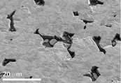
도 4a 내지 도 4e는 본 발명의 일 실시예에 따른 박막 구조체에서 질화갈륨의 기둥을 촬영한 사진들이다.
도 5a 내지 도 5b는 본 발명의 일 실시예에 따른 박막 구조체에서 질화갈륨에 대한 이미지들이다.
도 6a 내지 도 6g는 본 발명의 비교예에 따른 박막 구조체의 제조방법에서 사파이어 기판 상에 질화갈륨을 바로 형성한 구조체를 촬영한 이미지들이다.
도 7의 (a)는 본 발명의 비교예에 따른 박막 구조체의 제조방법에서 질화갈륨/사파이어 구조체의 TEM 이미지와 이에 대응되는 변형률 맵을 나타내는 도면이고, 도 7의 (b)는 본 발명의 일 실시예에 따른 박막 구조체의 제조방법에서 산화규소/사파이어 구조체의 TEM 이미지와 이에 대응되는 변형률 맵을 나타내는 도면이다.BRIEF DESCRIPTION OF DRAWINGS FIG. 1 is a conceptual illustration of the structure of a thin film structure according to an embodiment of the present invention; FIG.
FIGS. 2A and 2B are diagrams illustrating a method of manufacturing a thin film structure according to an embodiment of the present invention.
3A is a photograph of a structure in which a silicon oxide layer is formed on a sapphire substrate in a method of manufacturing a thin film structure according to an embodiment of the present invention.
FIG. 3B is a photograph of gallium nitride formed on a silicon oxide layer / sapphire substrate structure in the method of manufacturing a thin film structure according to an embodiment of the present invention.
FIG. 3C is a graph showing a result of measuring the concentration of silicon in sapphire after gallium nitride is formed in the method of manufacturing a thin film structure according to an embodiment of the present invention. FIG.
4A to 4E are photographs of pillars of gallium nitride in the thin film structure according to an embodiment of the present invention.
5A and 5B are images of gallium nitride in the thin film structure according to an embodiment of the present invention.
6A to 6G are images of a structure formed by directly forming gallium nitride on a sapphire substrate in a method of manufacturing a thin film structure according to a comparative example of the present invention.
7 (a) is a view showing a TEM image of a gallium nitride / sapphire structure and a corresponding strain map in the method of manufacturing a thin film structure according to a comparative example of the present invention, and Fig. 7 (b) FIG. 3 is a TEM image of a silicon oxide / sapphire structure and a strain map corresponding thereto in the method of manufacturing a thin film structure according to an embodiment.
이하, 첨부된 도면을 참조하여 본 발명의 바람직한 여러 실시예들을 상세히 설명하기로 한다.Hereinafter, preferred embodiments of the present invention will be described in detail with reference to the accompanying drawings.
본 발명의 일부 실시예들은 당해 기술 분야에서 통상의 지식을 가진 자에게 본 발명을 더욱 완전하게 설명하기 위하여 제공되는 것이며, 하기 실시예는 여러 가지 다른 형태로 변형될 수 있으며, 본 발명의 범위가 하기 실시예에 한정되는 것은 아니다. 오히려 이들 실시예들은 본 개시를 더욱 충실하고 완전하게 하고, 당업자에게 본 발명의 사상을 완전하게 전달하기 위하여 제공되는 것이다. 또한, 도면에서 각 층의 두께나 크기는 설명의 편의 및 명확성을 위하여 과장된 것이다.Some embodiments of the present invention are provided to more fully describe the present invention to those skilled in the art, and the following embodiments may be modified in various other forms, The present invention is not limited to the following examples. Rather, these embodiments are provided so that this disclosure will be more thorough and complete, and will fully convey the concept of the invention to those skilled in the art. In the drawings, the thickness and size of each layer are exaggerated for convenience and clarity of explanation.
명세서 전체에 걸쳐서, 막, 영역 또는 기판과 같은 하나의 구성요소가 다른 구성요소 "상에", "연결되어", "적층되어" 또는 "커플링되어" 위치한다고 언급할 때는, 상기 하나의 구성요소가 직접적으로 다른 구성요소 "상에", "연결되어", "적층되어" 또는 "커플링되어" 접합하거나, 그 사이에 개재되는 또 다른 구성요소들이 존재할 수 있다고 해석될 수 있다. 반면에, 하나의 구성요소가 다른 구성요소 "직접적으로 상에", "직접 연결되어", 또는 "직접 커플링되어" 위치한다고 언급할 때는, 그 사이에 개재되는 다른 구성요소들이 존재하지 않는다고 해석된다. 동일한 부호는 동일한 요소를 지칭한다. 본 명세서에서 사용된 바와 같이, 용어 "및/또는"은 해당 열거된 항목 중 어느 하나 및 하나 이상의 모든 조합을 포함한다.It is to be understood that throughout the specification, when an element such as a film, region or substrate is referred to as being "on", "connected to", "laminated" or "coupled to" another element, It is to be understood that elements may be directly "on", "connected", "laminated" or "coupled" to another element, or there may be other elements intervening therebetween. On the other hand, when one element is referred to as being "directly on", "directly connected", or "directly coupled" to another element, it is interpreted that there are no other components intervening therebetween do. Like numbers refer to like elements. As used herein, the term "and / or" includes any and all combinations of one or more of the listed items.
본 명세서에서 제 1, 제 2 등의 용어가 다양한 부재, 부품, 영역, 층들 및/또는 부분들을 설명하기 위하여 사용되지만, 이들 부재, 부품, 영역, 층들 및/또는 부분들은 이들 용어에 의해 한정되지 않음은 자명하다. 이들 용어는 하나의 부재, 부품, 영역, 층 또는 부분을 다른 영역, 층 또는 부분과 구별하기 위하여만 사용된다. 따라서, 이하 상술할 제 1 부재, 부품, 영역, 층 또는 부분은 본 발명의 가르침으로부터 벗어나지 않고서도 제 2 부재, 부품, 영역, 층 또는 부분을 지칭할 수 있다.Although the terms first, second, etc. are used herein to describe various elements, parts, regions, layers and / or sections, these elements, parts, regions, layers and / It is self-evident. These terms are only used to distinguish one member, component, region, layer or section from another region, layer or section. Thus, a first member, component, region, layer or section described below may refer to a second member, component, region, layer or section without departing from the teachings of the present invention.
또한, "상의" 또는 "위의" 및 "하의" 또는 "아래의"와 같은 상대적인 용어들은 도면들에서 도해되는 것처럼 다른 요소들에 대한 어떤 요소들의 관계를 기술하기 위해 여기에서 사용될 수 있다. 상대적 용어들은 도면들에서 묘사되는 방향에 추가하여 소자의 다른 방향들을 포함하는 것을 의도한다고 이해될 수 있다. 예를 들어, 도면들에서 소자가 뒤집어 진다면(turned over), 다른 요소들의 상부의 면 상에 존재하는 것으로 묘사되는 요소들은 상기 다른 요소들의 하부의 면 상에 방향을 가지게 된다. 그러므로, 예로써 든 "상의"라는 용어는, 도면의 특정한 방향에 의존하여 "하의" 및 "상의" 방향 모두를 포함할 수 있다. 소자가 다른 방향으로 향한다면(다른 방향에 대하여 90도 회전), 본 명세서에 사용되는 상대적인 설명들은 이에 따라 해석될 수 있다.Also, relative terms such as "top" or "above" and "under" or "below" can be used herein to describe the relationship of certain elements to other elements as illustrated in the Figures. Relative terms are intended to include different orientations of the device in addition to those depicted in the Figures. For example, in the figures the elements are turned over so that the elements depicted as being on the top surface of the other elements are oriented on the bottom surface of the other elements. Thus, the example "top" may include both "under" and "top" directions depending on the particular orientation of the figure. If the elements are oriented in different directions (rotated 90 degrees with respect to the other direction), the relative descriptions used herein can be interpreted accordingly.
본 명세서에서 사용된 용어는 특정 실시예를 설명하기 위하여 사용되며, 본 발명을 제한하기 위한 것이 아니다. 본 명세서에서 사용된 바와 같이, 단수 형태는 문맥상 다른 경우를 분명히 지적하는 것이 아니라면, 복수의 형태를 포함할 수 있다. 또한, 본 명세서에서 사용되는 경우 "포함한다(comprise)" 및/또는 "포함하는(comprising)"은 언급한 형상들, 숫자, 단계, 동작, 부재, 요소 및/또는 이들 그룹의 존재를 특정하는 것이며, 하나 이상의 다른 형상, 숫자, 동작, 부재, 요소 및/또는 그룹들의 존재 또는 부가를 배제하는 것이 아니다.The terminology used herein is for the purpose of describing particular embodiments only and is not intended to be limiting of the invention. As used herein, the singular forms "a," "an," and "the" include singular forms unless the context clearly dictates otherwise. Also, " comprise "and / or" comprising "when used herein should be interpreted as specifying the presence of stated shapes, numbers, steps, operations, elements, elements, and / And does not preclude the presence or addition of one or more other features, integers, operations, elements, elements, and / or groups.
이하, 본 발명의 일부 실시예들은 본 발명의 이상적인 실시예들을 개략적으로 도시하는 도면들을 참조하여 설명한다. 도면들에 있어서, 예를 들면, 제조 기술 및/또는 공차(tolerance)에 따라, 도시된 형상의 변형들이 예상될 수 있다. 따라서, 본 발명 사상의 실시예는 본 명세서에 도시된 영역의 특정 형상에 제한된 것으로 해석되어서는 아니 되며, 예를 들면 제조상 초래되는 형상의 변화를 포함하여야 한다.Hereinafter, some embodiments of the present invention will be described with reference to the drawings schematically illustrating ideal embodiments of the present invention. In the figures, for example, variations in the shape shown may be expected, depending on manufacturing techniques and / or tolerances. Accordingly, the embodiments of the present invention should not be construed as limited to the particular shapes of the regions shown herein, but should include, for example, changes in shape resulting from manufacturing.
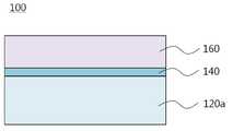
도 1은 본 발명의 일 실시예에 따른 박막 구조체의 구성을 개념적으로 도해하는 도면이다.BRIEF DESCRIPTION OF DRAWINGS FIG. 1 is a conceptual illustration of the structure of a thin film structure according to an embodiment of the present invention; FIG.
도 1을 참조하면, 본 발명의 일 관점에 따른 박막 구조체(100)는 지지기판(120a), 지지기판(120a) 상에 배치되는 중간층(140) 및 중간층(140) 상에 배치되는 에피층(160)을 구비한다. 지지기판(120a)은 제1물질을 포함하여 구성되며, 중간층(140)은 제2물질을 포함하여 구성되며, 에피층(160)은 제3물질을 포함하여 구성될 수 있다. 이 경우, 상기 제2물질의 체적탄성계수(bulk modulus)는 상기 제1물질의 체적탄성계수 및/또는 상기 제3물질의 체적탄성계수보다 더 작을 수 있다. 한편, 중간층(140)의 전단탄성계수는 지지기판(120a)의 전단탄성계수 및/또는 에피층(160)의 전단탄성계수보다 더 작을 수 있다.1, a
한편, 중간층(140)의 강성(elastic stiffness)은 에피층(160)의 강성보다 더 낮을 수 있으며, 나아가, 중간층(140)의 강성은 지지기판(120a) 및 에피층(160)의 강성보다 더 낮을 수 있다.The elastic stiffness of the
본 발명의 일 관점에 따른 박막 구조체(100)에서, 상기 제1물질을 포함하여 구성된 지지기판(120a)과 상기 제3물질을 포함하여 구성된 에피층(160) 사이의 격자 부정합(mismatch)에 기인하여 생성된 전위(dislocation)를 중간층(140)에서 수용할 수 있도록, 중간층(140)은 에피층(160)보다 탄성적으로 더 연성(elastically softer)일 수 있다. 따라서, 본 발명의 일 관점에 따른 박막 구조체(100)에서는 지지기판(120a)과 에피층(160) 사이의 격자 부정합에 기인하여 발생되는 결함의 적어도 일부가 에피층(160)이 아니라 중간층(140)에 수용되도록 구성하여 에피층(160) 내의 결함 밀도를 감소시킬 수 있다.In the
격자 부정합 구조체에서 변형(strain)을 제어하고 에피층(160)에서의 결함 밀도를 감소시키며 중간층(140)으로 격자 결함을 수용할 수 있다는 측면에서, 본 발명의 일 관점에 따른 박막 구조체(100)에서 중간층(140)은 컴플라이언트층(compliant layer) 또는 컴플라이언트 기판(compliant substrate)으로 이해될 수 있다.The
본 발명의 일 관점에 따른 박막 구조체(100)에서, 상기 제1물질은 화학성분이 Al2O3인 사파이어를 포함하고, 상기 제2물질은 규소(Si)를 포함하고, 상기 제3물질은 질화갈륨(GaN)을 포함할 수 있다. 이 경우, 중간층(140)은 사파이어에 규소가 확산된 층이거나 사파이어에 규소가 이온주입된 층일 수 있다. 중간층(140)에서 규소는 사파이어 내에 별도의 중간상이나 제2상을 형성하지 않고 불순물(impurity)로 존재할 수 있다. 예를 들어, 중간층(140)에서 규소는 사파이어 내에 매우 낮은 농도로 고용된 형태로 존재할 수 있다.In the
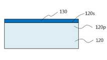
도 1을 참조하면, 본 발명의 다른 관점에 따른 박막 구조체(100)는 제1물질을 포함하여 구성되는 지지기판(120a), 및 지지기판(120a) 상에 배치되며 제3물질을 포함하여 구성되는 에피층(160)을 구비한다. 지지기판(120a)과 에피층(160) 사이에 개재되며, 제2물질을 포함하여 구성되는 중간층(140)은 지지기판(도 2의 120)의 상부(120p)에 형성될 수 있다. 즉, 중간층(140)은 상기 제2물질이 지지기판(120)의 상부면(120s)을 통하여 상부(120p)로 확산되거나 이온주입되어 형성될 수 있다. 중간층(140)의 역할이나 제1물질 내지 제3물질의 종류나 특성 등은 앞에서 이미 설명하였으므로 여기에서는 생략한다.Referring to FIG. 1, a
도 2a 및 도 2b는 본 발명의 일 실시예에 따른 박막 구조체의 제조방법을 도해하는 도면들이다.FIGS. 2A and 2B are diagrams illustrating a method of manufacturing a thin film structure according to an embodiment of the present invention.
도 1 및 도 2a를 참조하면, 본 발명의 일 실시예에 따른 박막 구조체(100)의 제조방법은 제1물질을 포함하여 구성된 지지기판(120)을 제공하는 단계; 지지기판(120) 상에 제2물질을 포함하여 구성된 임시층(temporary layer, 130)을 형성하는 단계; 및 임시층(130) 상에 제3물질을 포함하여 구성된 에피층(160)을 형성하는 단계;를 구비한다.Referring to FIGS. 1 and 2A, a method of manufacturing a
이 경우, 상기 제2물질의 체적탄성계수(bulk modulus)는 상기 제1물질의 체적탄성계수 및/또는 상기 제3물질의 체적탄성계수보다 더 작을 수 있다. 한편, 중간층(140)의 전단탄성계수는 지지기판(120a)의 전단탄성계수 및/또는 에피층(160)의 전단탄성계수보다 더 작을 수 있다.In this case, the bulk modulus of the second material may be smaller than the bulk modulus of the first material and / or the bulk modulus of elasticity of the third material. On the other hand, the shear modulus of elasticity of the
임시층(130) 상에 제3물질을 포함하는 에피층(160)을 형성하는 단계를, 섭씨 수 백 내지 수 천의 온도에서, 수행하는 동안, 임시층(130)에서 기인하는 상기 제2물질이 지지기판(120)의 상부면(120s)을 통하여 확산됨으로써 지지기판(120)의 상부(120p)에 상기 제2물질을 포함하여 구성된 중간층(140)이 형성될 수 있다. 이 과정에서 임시층(130)의 적어도 일부는 중간층(140)으로 전환되거나 소멸될 수 있다. 즉, 임시층(130)은 박막 구조체(100)를 형성하기 위한 제조방법의 중간단계에서만 존재하고 박막 구조체의 최종 구조에서는 존재하지 않을 수 있다.The step of forming an
상기 제1물질은 화학성분이 Al2O3인 사파이어를 포함하고, 상기 제2물질은 규소(Si)를 포함하고, 상기 제3물질은 질화갈륨(GaN)을 포함할 수 있다. 이 경우, 임시층(130)은 산화규소(SiO2)층을 포함할 수 있다. 예를 들어, 유기금속 화학기상증착법(MOCVD)에 의하여 질화갈륨을 형성하는 공정의 적어도 일부는 고온에서 수행될 수 있는데, 이 과정에서 임시층(130)을 구성하는 산화규소(SiO2) 중에서 규소가 지지기판(120)의 상부면(120s)을 통하여 지지기판(120)의 상부(120p)에 확산됨으로써 규소를 포함하여 구성된 중간층(140)이 지지기판(120)의 상부(120p)에 형성될 수 있다.The first material may include sapphire whose chemical composition is Al2 O3 , the second material may include silicon (Si), and the third material may include gallium nitride (GaN). In this case, the
한편, 본 발명의 변형된 실시예에 따르면, 임시층(130)으로 규소(Si)층을 전착이나 증착에 의하여 형성할 수 있다. 계속하여, 유기금속 화학기상증착법(MOCVD)에 의하여 질화갈륨을 형성하는 공정의 적어도 일부는 고온에서 수행될 수 있는데, 이 과정에서 임시층(130)을 구성하는 상기 규소층 중에서 규소가 지지기판(120)의 상부면(120s)을 통하여 지지기판(120)의 상부(120p)에 확산됨으로써 규소를 포함하여 구성된 중간층(140)이 지지기판(120)의 상부(120p)에 형성될 수 있다.Meanwhile, according to the modified embodiment of the present invention, a silicon (Si) layer can be formed by electrodeposition or vapor deposition as the
도 1 및 도 2b를 참조하면, 본 발명의 일 실시예에 따른 박막 구조체(100)의 다른 제조방법은 제1물질을 포함하여 구성된 지지기판(120)을 제공하는 단계; 지지기판(120)의 상부면(120s)을 통하여 제2물질을 이온주입(ion-implant, 135)함으로써 지지기판(120)의 상부(120p)에 상기 제2물질을 포함하여 구성된 중간층(140)을 형성하는 단계; 및 중간층(140) 상에 제3물질을 포함하여 구성된 에피층(160)을 형성하는 단계;를 포함할 수 있다. 본 실시예에서는 중간층(140)을 형성하기 위하여 임시층(130)을 별도로 도입하지 않고 지지기판(120)의 상부(120p)에 제2물질을 직접 이온주입(135)하여 중간층(140)을 구현하므로, 도 2a와 달리, 에피층(160)을 형성하기 이전에 중간층(140)이 이미 형성될 수 있다. 이온주입 공정의 조건을 변경함으로써 중간층(140) 내에서 상기 제2물질의 농도 프로파일을 적절하게 제어할 수 있다. 중간층(140)의 역할이나 제1물질 내지 제3물질의 종류나 특성 등은 앞에서 이미 설명하였으므로 여기에서는 생략한다.Referring to FIGS. 1 and 2B, another method of manufacturing a
한편, 상술한 박막 구조체(100)는 다양한 형태의 전자기 소자에 적용될 수 있다. 상기 전자기 소자는, 예를 들어, 박막 소자, 나노 소자, 반도체 소자, 메모리 소자, 분자 소자, 광소자, 광전 소자, 디스플레이 소자, 및 디지털 소자 중에서 선택된 적어도 어느 하나를 포함할 수 있다.
On the other hand, the
이하, 본 발명의 이해를 돕기 위해서 실시예를 제공한다. 다만, 하기의 실시예들은 본 발명의 이해를 돕기 위한 것일 뿐, 본 발명이 아래의 실시예들에 의해서 한정되는 것은 아니다.Hereinafter, embodiments are provided to facilitate understanding of the present invention. It should be understood, however, that the following examples are for the purpose of promoting understanding of the present invention, but the present invention is not limited by the following examples.
도 3a는 본 발명의 일 실시예에 따른 박막 구조체의 제조방법에서 사파이어 기판 상에 원자층증착(ALD) 공정으로 산화규소층이 형성된 구조체를 촬영한 고각도 산란 암시야 주사투과전자현미경(High angle annular dark field(HAADF)-STEM) 이미지이며, 도 3b는 본 발명의 일 실시예에 따른 박막 구조체의 제조방법에서 산화규소층/사파이어 기판 구조체 상에 형성된 질화갈륨을 촬영한 주사전자현미경(SEM) 이미지이며, 도 3c는 본 발명의 일 실시예에 따른 박막 구조체의 제조방법에서 유기금속 기상화학증착(MOCVD)에 의하여 질화갈륨이 형성된 이후에 사파이어 내에 규소의 농도를 측정한 이차 이온 질량분석(SIMS) 프로파일을 나타낸 그래프이다.FIG. 3A is a schematic view showing a high angle scattering dark field scanning electron microscope (SEM) image of a structure in which a silicon oxide layer is formed by an atomic layer deposition (ALD) process on a sapphire substrate in a method of manufacturing a thin film structure according to an embodiment of the present invention. FIG. 3B is a scanning electron microscope (SEM) image of gallium nitride formed on a silicon oxide layer / sapphire substrate structure in the method of manufacturing a thin film structure according to an embodiment of the present invention. FIG. 3c is a graph showing the results of a secondary ion mass spectrometry (SIMS) analysis in which gallium nitride is formed by metal organic chemical vapor deposition (MOCVD) in a method of manufacturing a thin film structure according to an embodiment of the present invention, ) Profile.
도 3a를 참조하면, 유기금속 기상화학증착(MOCVD)에 의하여 질화갈륨을 형성하기 이전에, 사파이어 기판 상에 원자층증착(ALD) 공정으로 공칭두께(nominal thickness) 0.5 nm의 산화규소층을 형성한다. 상기 산화규소층은 도 2a에 도시된 임시층(130)에 대응된다. 한편, 도 3a의 이미지는 산화규소층의 두께가 0.53 ± 0.1nm인 부분을 나타내지만 두께가 균일하지 않음을 보여준다.Referring to FIG. 3A, a silicon oxide layer having a nominal thickness of 0.5 nm is formed by an atomic layer deposition (ALD) process on a sapphire substrate prior to the formation of gallium nitride by metal organic chemical vapor deposition (MOCVD) do. The silicon oxide layer corresponds to the
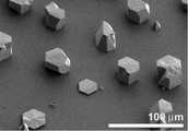
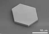
도 3b를 참조하면, 유기금속 기상화학증착(MOCVD)에 의하여 형성된 질화갈륨의 일부는 육방정계 피라미드(hexagonal pyramid)의 형태를 가질 뿐만 아니라, 200nm 내지 10㎛ 범위를 가지는 다양한 높이의 육방정계 기둥(hexagonal column)으로 구성됨을 확인할 수 있다.Referring to FIG. 3B, a part of the gallium nitride formed by metal organic chemical vapor deposition (MOCVD) has a hexagonal pyramid shape, as well as hexagonal pyramids having various heights ranging from 200 nm to 10 μm hexagonal column).
흥미롭게도, 유기금속 기상화학증착(MOCVD)에 의하여 질화갈륨을 형성한 이후에는 도 3a와 같은 산화규소층이 관찰되지 않았다. 대신에, 도 3c와 같이, 이차 이온 질량분석(SIMS)에 의하여 사파이어 기판의 상부에 소량의 규소를 포함하는 박막층이 형성된 것을 확인하였다. 이차 이온 질량분석(SIMS)은 질화갈륨 기둥에 의하여 덮이지 않은 영역에서 수행되었다. 그래프의 우측 세로축은 알루미늄과 산소의 프로파일에 대한 단위를 나타내며, 좌측 세로축은 규소의 프로파일에 대한 단위를 나타낸다. 도 3c를 참조하면, 표면에서의 규소 농도는 약 1020cm-3 이며, 2.9 nm의 깊이에서 규소의 최대 농도인 1.68 x 1020cm-3 가 나타난다. 사파이어의 밀도가 약 1.17 x 1023cm-3인 점을 감안하면, 표면에서의 규소 농도는 0.085 at% 에 해당한다.Interestingly, after the formation of gallium nitride by metal organic chemical vapor deposition (MOCVD), the silicon oxide layer as shown in FIG. 3A was not observed. Instead, as shown in FIG. 3C, it was confirmed by the secondary ion mass spectrometry (SIMS) that a thin film layer containing a small amount of silicon was formed on the sapphire substrate. Secondary ion mass spectrometry (SIMS) was performed in areas not covered by gallium nitride pillars. The vertical axis on the right side of the graph represents the unit for the profile of aluminum and oxygen, and the vertical axis on the left represents the unit for the profile of silicon. Referring to FIG. 3C, the silicon concentration at the surface is about 1020 cm-3 , and at a depth of 2.9 nm, the maximum concentration of silicon is 1.68 x 1020 cm-3 . Considering that the density of sapphire is about 1.17 x 10 <23 > cm <-3 & gt ;, the silicon concentration at the surface corresponds to 0.085 at%.
도 4a 내지 도 4e는 본 발명의 일 실시예에 따른 박막 구조체에서 질화갈륨의 기둥을 촬영한 사진들로서, 도 4a는 도 3a에 나타난 동일 영역으로부터 획득한 팬크로매틱 음극선 발광(panchromatic cathodoluminescence(CL)) 이미지이며, 도 4b는 도 4a에서 백색 화살표가 표시하는 낮은 기둥의 틸트뷰 상태로 확대한 주사전자현미경 이미지이며, 도 4c는 이에 대응하는 음극선 발광 이미지이며, 도 4d는 다른 기둥의 틸트뷰 상태의 주사전자현미경 이미지이며, 도 4e는 도 4d에 대응하는 음극선 발광 이미지이다. 질화갈륨 기둥들은 대략 (0001) 상면과 {1-100} 면들로 이루어진 육각기둥의 형태를 띤다.FIGS. 4A to 4E are photographs of pillar of gallium nitride in the thin film structure according to an embodiment of the present invention. FIG. 4A is a graph showing the panchromatic cathodoluminescence (CL) image obtained from the same region shown in FIG. FIG. 4B is a scanning electron microscope image enlarged to a tilt view state of a low column indicated by a white arrow in FIG. 4A, FIG. 4C is a corresponding cathode ray emission image, FIG. Electron microscope image, and FIG. 4E is a cathode ray emission image corresponding to FIG. 4D. The gallium nitride pillars are in the form of hexagonal columns consisting of approximately (0001) upper surface and {1-100} planes.
도 4b를 참조하면, 질화갈륨의 다소 낮은 육방정계 기둥들은 400nm 내지 1.2㎛ 높이를 가지며 5㎛ 내지 30㎛의 길이를 가진다. 도 4c에 나타난 다크 스팟 콘트라스트들(dark spot contrasts)은 관통 전위나 다른 형태의 선결함들에 대응될 수 있다. 도 4c에 나타난 회색 화살표가 가리키는 것처럼, 질화갈륨 내에 결함들은 거의 관찰되지 않거나, 또는 도 4e와 같이 결함이 전혀 나타나지 않았다. 이는 질화갈륨 내에 전위가 거의 없다는 것을 의미할 수 있다. 이러한 놀라운 결과는 투과전자현미경(TEM)에 의해서도 확인할 수 있다.Referring to FIG. 4B, the somewhat lower hexagonal columns of gallium nitride have a height of 400 nm to 1.2 탆 and a length of 5 탆 to 30 탆. The dark spot contrasts shown in Figure 4c may correspond to threading dislocations or other types of line defects. As indicated by the gray arrows in Fig. 4C, few defects were observed in gallium nitride, or no defects were seen as in Fig. 4e. This may mean that there is little potential in the gallium nitride. This surprising result can also be confirmed by transmission electron microscopy (TEM).
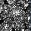
도 5a 내지 도 5d는 본 발명의 일 실시예에 따른 박막 구조체에서 질화갈륨에 대한 이미지들로서, 도 5a 및 도 5b는 각각 g=0-110 조건 및 g=0002 조건에서 [-2110] 영역축 근처에서 획득한 질화갈륨 기둥의 (g-3g) 약빔 암시야상(Weak-beam dark-field image)이며, 도 5c는 [-2110] 영역축 근처에서 획득한 동일한 질화갈륨 기둥의 단면 투과전자현미경(TEM) 이미지이다.5A and 5D are images for gallium nitride in the thin film structure according to an embodiment of the present invention, FIGS. 5A and 5B are graphs showing the relationship between [-2110] domain axes near g = 0-110 and g = 5c is a cross-sectional transmission electron microscope (TEM) of the same gallium nitride column obtained near the [-2110] domain axis, and FIG. 5C is a cross- ) Image.
도 5a 및 도 5b를 참조하면, g=0-110 조건 및 g=0002 조건에서 질화갈륨의 [-2110] 영역축 근처에서 획득한 g-3g 약빔 암시야상(Weak-beam dark-field image) 단면 투과전자현미경 이미지에 의하여 결함들과 결함 밀도들이 관찰, 측정될 수 있다. 그러나 모든 기둥들에서 결함들은 검출되지 않았다.5a and 5b, a g-3g weak-field dark-field image obtained near the [-2110] domain axis of gallium nitride under g = 0-110 condition and g = 0002 condition Defects and defect densities can be observed and measured by transmission electron microscopy images. However, no defects were detected in all the columns.
질화갈륨/사파이어 계면 근처에서의 국부적인 변형률(strain) 성분들을 측정하기 위하여, GPA(Geometric Phase Analysis) 및 TEM 변형률 매핑을 이용할 수 있다. 본 발명의 일 실시예에 따른 산화규소층/사파이어 기판의 경우와 비교하기 위하여, 본 발명의 비교예에서는 베어(bare) 사파이어 기판 상에 질화갈륨을 바로 형성하였다.Geometric phase analysis (GPA) and TEM strain mapping can be used to measure local strain components near the gallium nitride / sapphire interface. In comparison with the silicon oxide / sapphire substrate according to an embodiment of the present invention, gallium nitride was directly formed on a bare sapphire substrate in the comparative example of the present invention.
도 6a 내지 도 6g는 본 발명의 비교예에 따른 박막 구조체의 제조방법에서 사파이어 기판 상에 질화갈륨을 바로 형성한 구조체를 촬영한 이미지들이다. 도 6a를 참조하면, 사파이어 기판 상에 직접 형성된 질화갈륨은 필름의 형태를 띠며, 도 6b 및 도 6c를 참조하면, 사파이어 기판 상에 직접 형성된 질화갈륨은 높은 밀도의 결함들을 가지고 있음을 확인할 수 있다.6A to 6G are images of a structure formed by directly forming gallium nitride on a sapphire substrate in a method of manufacturing a thin film structure according to a comparative example of the present invention. Referring to FIG. 6A, the gallium nitride formed directly on the sapphire substrate is in the form of a film. Referring to FIGS. 6B and 6C, gallium nitride formed directly on the sapphire substrate has high density defects .
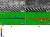
도 7의 (a)는 본 발명의 비교예에 따른 박막 구조체의 제조방법에서 질화갈륨/사파이어 구조체의 TEM 이미지와 이에 대응되는 변형률 맵을 나타내는 도면으로서, 상측에 배치된 도면은 베어 사파이어 기판 상에 질화갈륨이 직접 형성된 질화갈륨/사파이어 계면의 고해상 투과전자현미경(TEM) 이미지이고, 하측에 배치된 도면은 이에 대응하여 GPA에 의하여 획득한 εxx 변형률 맵(strain map)이다. 도 7의 (b)는 본 발명의 일 실시예에 따른 박막 구조체의 제조방법에서 산화규소/사파이어 구조체의 TEM 이미지와 이에 대응되는 변형률 맵을 나타내는 도면으로서, 상측에 배치된 도면은 산화규소층/사파이어 기판 상에 질화갈륨이 형성된 계면의 고해상 투과전자현미경(TEM) 이미지이고, 하측에 배치된 도면은 이에 대응하여 획득한 εxx 변형률 맵(strain map)이다. x 방향은 상기 계면에 평행하며, y 방향은 상기 계면에 수직이다. 컬러바는 -0.4에서 0.6까지의 범위를 가지는 전체 변형률을 가리킨다.FIG. 7A is a diagram showing a TEM image of a gallium nitride / sapphire structure and a strain map corresponding thereto in the method of manufacturing a thin film structure according to a comparative example of the present invention, (TEM) image of a gallium nitride / sapphire interface where gallium nitride is directly formed, and the diagram arranged on the lower side corresponds to an εxx strain map obtained by GPA. FIG. 7 (b) is a view showing a TEM image of a silicon oxide / sapphire structure and a strain map corresponding to the silicon oxide / sapphire structure in the method of manufacturing a thin film structure according to an embodiment of the present invention, High-resolution transmission electron microscope (TEM) image of the interface at which gallium nitride is formed on the sapphire substrate, and the lower diagram is the corresponding εxx strain map obtained. The x direction is parallel to the interface and the y direction is perpendicular to the interface. The color bar indicates the total strain in the range of -0.4 to 0.6.
도 7의 (a)를 참조하면, 베어 사파이어 기판에 대해서는, 미스핏 전위(MD, misfit dislocation)가 질화갈륨/사파이어 계면에서 질화갈륨 방향으로 떨어져 나타나며, 이에 반하여, 도 7의 (b)를 참조하면, 규소가 확산된 사파이어 기판에 대해서는, 미스핏 전위가 사파이어 방향으로 후퇴된다. 도 7을 참조하면, εxx 변형률 맵은 전위들의 코어 위치를 정확하게 표시한다.Referring to FIG. 7A, a misfit dislocation (MD) appears at a gallium nitride / sapphire interface in the direction of gallium nitride in a bare sapphire substrate. On the other hand, referring to FIG. 7B, Then, for the sapphire substrate on which silicon is diffused, the misfit potential is retracted in the sapphire direction. Referring to Fig. 7, the?Xx strain map accurately represents the core position of the potentials.
도 7의 (a)를 참조하면, 질화갈륨 내의 전위들 사이의 이격거리는 1.01±0.13 nm이며, 계면에서 전위까지의 거리는 약 0.21±0.1 nm인 것으로 나타났으며, 도 7의 (b)를 참조하면, 질화갈륨 내의 전위들 사이의 이격거리는 1.21±0.18 nm이며, 계면에서 전위까지의 거리는 약 0.45±0.18 nm인 것으로 나타난다.Referring to Figure 7 (a), the distance between the dislocations in the gallium nitride is 1.01 ± 0.13 nm, and the distance from the interface to the dislocation is about 0.21 ± 0.1 nm, see FIG. 7 (b) , The distance between the dislocations in the gallium nitride is 1.21 ± 0.18 nm and the distance from the interface to the dislocation is about 0.45 ± 0.18 nm.
지금까지 살펴본 것처럼, 산화규소/사파이어 기판 상에 형성된 질화갈륨이 섬 구조(island structure)를 나타내는 현상(예를 들어, 도 3b 참조)과 베어 사파이어 기판 상에 형성된 질화갈륨이 필름의 형태를 나타내는 현상(예를 들어, 도 6a 참조)을 고려할 때, 규소의 확산에 의하여 표면에너지에 대한 계면에너지의 비율이 감소되고 이는 질화갈륨의 핵생성을 지연시킨다는 것을 유추할 수 있다. 따라서, 질화갈륨은 규소가 풍부한 영역에서보다 규소가 부족한 영역에서 더 빨리 핵생성이 일어나는 경향을 가지며, 이는, 도 3b와 같이, 질화갈륨의 기둥들이 불균일한 높이를 가지게 한다. 발명자는 높은 기둥의 질화갈륨은 결함 밀도가 높으며 규소가 부족한 영역에서 핵생성이 일어나며, 낮은 기둥의 질화갈륨은 전위가 거의 또는 전혀 없으며 상대적으로 규소가 풍부한 영역에서 생성됨을 확인하였다.As has been described so far, a phenomenon in which gallium nitride formed on a silicon oxide / sapphire substrate exhibits an island structure (for example, see FIG. 3b) and a phenomenon in which gallium nitride formed on a bear sapphire substrate exhibits a shape of a film (See, for example, FIG. 6A), it can be deduced that the diffusion of silicon reduces the ratio of interfacial energy to surface energy, which delays the nucleation of gallium nitride. Thus, gallium nitride tends to nucleate faster in regions where silicon is less than in regions rich in silicon, which causes the columns of gallium nitride to have non-uniform heights, as shown in FIG. 3B. The inventor has found that gallium nitride in the high column is nucleated in regions where the defect density is high and the silicon is insufficient, and gallium nitride in the low column is generated in a region where there is little or no dislocation and relatively silicon-rich region.
두 결정질 상들 사이의 계면에서의 부정합은 계면에서 미스핏 전위들에 의하여 수용될 수 있다. 그러나, 두 결정질의 전단탄성계수(shear modulus)가 서로 다른 경우에는, 전위 에너지가 더욱 현저한 컴플라이언트 영역 내에서 더 낮아지므로, 미스핏 전위들은 계면에서 이격거리를 가지고 더 낮은 전단탄성계수를 가지는 영역으로 이동된다.Mismatches at the interface between the two crystalline phases can be accommodated by misfit dislocations at the interface. However, when the shear moduli of the two crystals are different, the potential energy becomes lower in the more pronounced compliant region, so that the misfit dislocations have regions with spacing at the interface and a lower shear modulus .
c-면의 사파이어 상의 에피택셜 c-GaN의 경우에서, c-면들에 대하여 각각의 전단탄성계수들들을 비교할 수 있다. 우선, 두 물질들의 컴플라이언스(elastic compliance)를 비교하면, 사파이어(α-Al2O3)에 대하여, 298K의 온도에서, S11=0.002351, S33=0.002173, S44=0.006941, S12=-0.0006992, S13=-0.0003857, S14=0.0004745의 값(단위:GPa-1)을 가지며, 우르차이트(wurtzite) 결정 구조를 가지는 질화갈륨에 대하여, S11=0.003196, S33=0.002764,S44=0.010684,S12=-0.001115, S13=-0.0004323의 값(단위:GPa-1)을 가진다. 기준면 상의 전단 방향에 독립적인 값을 가지는 기준면 상의 전단탄성계수(=1/S44)는 사파이어가 144 GPa의 값을 가지며, 질화갈륨이 94 GPa의 값을 가진다. 이에 따르면 질화갈륨이 사파이어보다 더 컴플라이언트함을 알 수 있다. 앞에서 살펴본 바와 같이, 베어 사파이어의 경우에서 상기 계면에서 질화갈륨 방향으로 미스핏 전위들이 이동하는 것은 우르차이트(wurtzite) 결정 구조를 가지는 질화갈륨이 기준면 상에서 사파이어보다 더 낮은 전단탄성계수를 가지기 때문이다.In the case of epitaxial c-GaN on the c-plane sapphire, we can compare the respective shear moduli for the c-planes. First, when comparing the compliance (elastic compliance) of the two materials, with respect to the sapphire(α-Al 2 O 3) , at a temperature of298K, S 11 = 0.002351, S 33 = 0.002173, S 44 = 0.006941, S 12 = -0.0006992, S 13 = -0.0003857, S 14 = 0.0004745 values of: having the (in GPa-1), with respect to the gallium nitride has a bit difference Ur (wurtzite) crystalstructure, S 11 = 0.003196, S 33 = 0.002764, S44 = 0.010684, S12 = -0.001115, and S13 = -0.0004323 (unit: GPa-1 ). The shear modulus (= 1 / S44 ) on the reference plane having a value independent of the shear direction on the reference plane has a value of 144 GPa for sapphire and a value of 94 GPa for gallium nitride. It can be seen that gallium nitride is more compliant than sapphire. As described above, the migration of misfit dislocations in the direction of the gallium nitride from the interface in the case of bare sapphire is because the gallium nitride having a wurtzite crystal structure has a lower shear modulus than the sapphire on the reference plane .
이와 비교하여, 규소가 소량첨가된 사파이어는 순수한 사파이어보다 전단탄성계수가 더 낮다. 또한, 규소가 소량첨가된 사파이어는 규소가 소량첨가된 사파이어 상의 질화갈륨보다 전단탄성계수가 더 낮다. 이에 의하여, 미스핏 전위가 질화갈륨에서 규소가 소량첨가된(예를 들어, 규소가 확산되거나 이온주입된) 사파이어 방향으로 내려온다.In comparison, sapphire with a small amount of silicon added has a lower shear modulus than pure sapphire. In addition, the sapphire having a small amount of silicon added has a lower shear modulus than the sapphire-type gallium nitride to which a small amount of silicon is added. As a result, the misfit dislocation comes down to the sapphire direction in which a small amount of silicon is added (for example, silicon is diffused or ion implanted) in gallium nitride.
규소의 대칭성(cubic symmetry)이 사파이어의 대칭성(trigonal symmetry)와 다르지만, 규소의 컴플라이언스(compliance)가 사파이어의 컴플라이언스보다 더 높다. 즉, 규소는 298K의 온도에서, S11=0.007685, S44=0.012563, S12=-0.002139의 값(단위:GPa-1)을 가지므로, 규소의 체적탄성계수(bulk modulus)는 [3(S11+2S12)]-1으로 계산되어 98 GPa의 값을 가지며, 사파이어의 체적탄성계수는 [2(S11+S12+2S13)+S33]-1으로 계산되어 254 GPa의 값을 가진다. 이것은 규소가 사파이어보다 더 컴플라언트함을 의미하며, 다르게 표현하면, 규소가 사파이어보다 더 탄성적으로 연하다(elastically soft)는 것을 의미한다. 여기에서, 행렬 Sij는 탄성 컴플라이언스(elastic compliance)를 나타내는 행렬로서, 이를 역변환(inverse matrix)하면 강성(elastic stiffness)을 나타내는 행렬 Cij를 구할 수 있다.Although the cubic symmetry of silicon differs from the symmetry of sapphire, the compliance of silicon is higher than the compliance of sapphire. That is, since silicon has a value (units: GPa-1 ) of S11 = 0.007685, S44 = 0.012563 and S12 = -0.002139 at a temperature of 298K, the bulk modulus of silicon is [ 2S11 + S12)] is calculated as-1 has a value of 98 GPa, a bulk modulus sapphire[2 (S 11 + S 12 + 2S 13) + S 33] is calculated and a value of-1 of 254 GPa . This means that silicon is more compressible than sapphire and, in other words, it means that silicon is more elastically soft than sapphire. Here, the matrix Sij is a matrix representing elastic compliance, and a matrix Cij representing an elastic stiffness can be obtained by inverse matrixing the matrix Sij .
한편, 우르차이트(wurtzite) 결정 구조를 가지는 질화갈륨의 대칭성(hexagonal symmetry)을 고려하면, 질화갈륨은 298K의 온도에서, S11=0.003196, S33=0.002764, S44=0.010684, S12=-0.001115, S13=-0.0004323의 값(단위:GPa-1)을 가지므로, 질화갈륨의 체적탄성계수(bulk modulus)는 [2(S11+S12+2S13)+S33]-1 으로 계산되어, 192.43 GPa의 값을 가진다. 이것은 규소가 질화갈륨보다 더 컴플라언트함을 의미하며, 다르게 표현하면, 규소가 질화갈륨보다 더 탄성적으로 연하다는 것을 의미한다.On the other hand, considering the hexagonal symmetry of gallium nitride having a wurtzite crystal structure, the gallium nitride has a composition of S11 = 0.003196, S33 = 0.002764, S44 = 0.010684, S12 = -0.001115 and S13 = -0.0004323 (unit: GPa-1 ), the bulk modulus of the gallium nitride is [2 (S11 + S12 + 2S13 ) + S33 ]-1 And has a value of 192.43 GPa. This means that silicon is more companion than gallium nitride, which, in other words, means that the silicon is more resilient than gallium nitride.
규소, 사파이어, 질화갈륨의 컴플라이언스는, 예를 들어, S11를 비교하여 보면, 각각, 0.007685, 0.002351, 0.003196이므로, 규소가 가장 연하고, 질화갈륨이 그 다음으로 연하다고 파악할 수 있다.Compliance of silicon, sapphire, gallium nitride, for example, Compared to S11, respectively, because the 0.007685, 0.002351, 0.003196, and the silicon is the lead, and gallium can determine that year to the next.
이러한 결과들을 종합하면, 규소가 별도의 중간상이나 제2상을 형성하지 않고 매우 소량으로 불순물로 사파이어에 부가되면, 사파이어가 더 컴플라이언트해짐을 유추할 수 있다. 따라서, 규소가 확산되거나 이온주입된 사파이어 표면층은 전위를 생성함으로써 사파이어와 질화갈륨 사이의 큰 부정합을 수용할 수 있다(도 7의 (b) 참조).Taken together, these results suggest that sapphire can be more compliant if silicon is added to the sapphire as an impurity in very small quantities without forming a separate intermediate or second phase. Therefore, the sapphire surface layer in which silicon is diffused or ion-implanted can accommodate a large mismatch between sapphire and gallium nitride by generating dislocations (see Fig. 7 (b)).
베어 사파이어 기판의 경우에서, 질화갈륨층은 필름의 형태를 가지지만 최대 5㎛ 직경의 작은 그레인으로 구성되며 많은 결함들을 가진다(도 6a 내지 도 6c 참조). 이에 비하여, 규소가 확산되거나 이온주입된 사파이어 기판의 경우에서 질화갈륨은, 전위의 생성 없이, 부정합이나 열적 응력에 내성을 가질 수 있다.In the case of a bare sapphire substrate, the gallium nitride layer is in the form of a film, but is composed of small grains of a maximum diameter of 5 mu m and has many defects (see Figs. 6A to 6C). On the other hand, in the case of a sapphire substrate in which silicon is diffused or implanted, gallium nitride may have resistance to mismatch or thermal stress without generating dislocations.
GPA를 이용하여 분석한 결과, 사파이어는 소량의 규소를 첨가함으로써 질화갈륨보다 탄성적으로 더 연성이 되며, 이를 통해 전위가 없는 질화갈륨을 형성할 수 있음을 확인할 수 있었다.As a result of analysis using GPA, it was confirmed that sapphire is elastically more ductile than gallium nitride by addition of a small amount of silicon, thereby forming gallium nitride having no dislocation.
앞서 설명한 바와 같이, 베어 사파이어 기판의 경우에서는, 형성된 질화갈륨이 사파이어 지지기판보다 더 컴플라언트하기 때문에 미스핏 전위들이 질화갈륨 방향으로 이동하거나 질화갈륨에서 생성된다. 발명자는 전위의 생성 및/또는 이동의 적어도 일부가 전단탄성계수(shear modulus)와 관련이 있으며, 사파이어 기판층의 전단탄성계수(shear modulus)가 질화갈륨 에피층의 전단탄성계수보다 더 크고, 나아가, 규소의 체적탄성계수(bulk modulus)가 사파이어의 체적탄성계수보다 작고, 규소의 체적탄성계수가 질화갈륨의 체적탄성계수보다 작다는 점에 착안하여, 규소가 소량첨가된(예를 들어, 확산되거나 이온주입되어 소량첨가된) 사파이어로 이루어진 컴플라이언트 기판을 사파이어 지지기판과 질화갈륨 사이에 도입하였으며, 상기 컴플라이언트 기판이 질화갈륨보다 더 컴플라이언트하기 때문에 미스핏 전위들이 상기 컴플라이언트 기판 방향으로 이동하거나 상기 컴플라이언트 기판에서 생성됨을 확인하였다. 전위가 질화갈륨 쪽이 아니라 규소가 소량첨가된 사파이어 기판 쪽으로 이동한다는 것은 컴플라이언트 기판의 전단탄성계수가 지지기판의 전단탄성계수 및 질화갈륨 에피층의 전단탄성계수보다 낮다는 것을 의미한다.As described above, in the case of a bare sapphire substrate, misfit dislocations move in the direction of gallium nitride or are generated in gallium nitride because gallium nitride formed is more conformant than the sapphire supporting substrate. The inventors have found that at least some of the generation and / or movement of the dislocations is related to shear modulus and that the shear modulus of the sapphire substrate layer is greater than the shear modulus of the gallium nitride epitaxial layer, , The bulk modulus of silicon is smaller than the bulk elastic modulus of sapphire and the bulk elastic modulus of silicon is smaller than the bulk modulus of gallium nitride. In view of the fact that a small amount of silicon is added (for example, diffusion Or a small amount of sapphire) is introduced between the sapphire substrate and the gallium nitride, and since the compliant substrate is more compliant than gallium nitride, the misfit dislocations move toward the compliant substrate Or produced on the compliant substrate. The fact that the dislocations are shifted toward the sapphire substrate to which silicon is added rather than to the gallium nitride means that the shear modulus of the compliant substrate is lower than the shear modulus of the supporting substrate and the shear modulus of the gallium nitride epitaxial layer.
본 발명은 도면에 도시된 실시예를 참고로 설명되었으나 이는 예시적인 것에 불과하며, 당해 기술분야에서 통상의 지식을 가진 자라면 이로부터 다양한 변형 및 균등한 다른 실시예가 가능하다는 점을 이해할 것이다. 따라서 본 발명의 진정한 기술적 보호 범위는 첨부된 특허청구범위의 기술적 사상에 의하여 정해져야 할 것이다.While the present invention has been described with reference to exemplary embodiments, it is to be understood that the invention is not limited to the disclosed exemplary embodiments, but, on the contrary, is intended to cover various modifications and equivalent arrangements included within the spirit and scope of the invention. Accordingly, the true scope of the present invention should be determined by the technical idea of the appended claims.
120, 120a : 지지기판
130 : 임시층
140 : 중간층
160 : 에피층120, 120a:
130: temporary layer
140: middle layer
160: Epi layer
Claims (19)
Translated fromKorean상기 지지기판 상에 배치되며 상기 제1물질과 제2물질을 포함하여 구성된 중간층(intermediate layer); 및
상기 중간층 상에 배치되며 제3물질을 포함하여 구성된 에피층(epilayer);을 구비하고,
상기 제2물질의 체적탄성계수는 상기 제1물질의 체적탄성계수 및 상기 제3물질의 체적탄성계수보다 더 작고, 상기 중간층의 전단탄성계수는 상기 지지기판의 전단탄성계수 및 상기 에피층의 전단탄성계수보다 더 작은, 박막 구조체.A supporting substrate comprising a first material;
An intermediate layer disposed on the support substrate and comprising the first material and the second material; And
And an epilayer disposed on the intermediate layer and configured to include a third material,
Wherein the bulk modulus of the second material is smaller than the bulk modulus of elasticity of the first material and the volume modulus of elasticity of the third material and the modulus of shear modulus of the intermediate layer is greater than the modulus of shear modulus of the support substrate and the shear modulus of the sheath Lt; RTI ID = 0.0 > elastic modulus. ≪ / RTI >
상기 중간층은 상기 제1물질과 상기 제3물질 사이의 격자 부정합(mismatch)에 기인하여 생성된 전위를 수용할 수 있도록,
상기 중간층은 상기 에피층보다 탄성적으로 더 연성(elastically softer)인, 박막 구조체.The method according to claim 1,
Wherein the intermediate layer is configured to accept a potential generated due to lattice mismatch between the first material and the third material,
Wherein the intermediate layer is elastically softer than the epi layer.
상기 제1물질은 사파이어(sapphire)를 포함하고, 상기 제2물질은 규소(Si)를 포함하고, 상기 제3물질은 질화갈륨(GaN)을 포함하는, 박막 구조체.The method according to claim 1,
Wherein the first material comprises sapphire, the second material comprises silicon (Si), and the third material comprises gallium nitride (GaN).
상기 중간층은 사파이어에 규소가 확산된 층 또는 사파이어에 규소가 이온주입된 층을 포함하는, 박막 구조체.The method of claim 3,
Wherein the intermediate layer comprises a layer in which silicon is diffused into sapphire or a layer in which silicon is ion-implanted in sapphire.
상기 지지기판 상에 배치되며, 상기 제1물질과 제2물질을 포함하여 구성된 컴플라이언트층(compliant layer); 및
상기 컴플라이언트층 상에 배치되며, 제3물질을 포함하여 구성된 에피층;을 구비하고,
상기 컴플라이언트층의 강성(elastic stiffness)은 상기 에피층의 강성보다 더 낮은 것을 특징으로 하는, 박막 구조체.A support substrate comprising a first material;
A compliant layer disposed on the support substrate, the compliant layer comprising the first material and the second material; And
And an epi layer disposed on the compliant layer and configured to include a third material,
Wherein the compliant layer has an elastic stiffness that is lower than the stiffness of the epilayer.
상기 컴플라이언트층의 강성은 상기 지지기판의 강성보다 더 낮은 것을 특징으로 하는, 박막 구조체.6. The method of claim 5,
Wherein the rigidity of the compliant layer is lower than the rigidity of the support substrate.
상기 제1물질은 사파이어(sapphire)를 포함하고, 상기 제2물질은 규소(Si)를 포함하고, 상기 제3물질은 질화갈륨(GaN)을 포함하는, 박막 구조체.6. The method of claim 5,
Wherein the first material comprises sapphire, the second material comprises silicon (Si), and the third material comprises gallium nitride (GaN).
상기 컴플라이언트층은 사파이어에 규소가 확산된 층 또는 사파이어에 규소가 이온주입된 층을 포함하는, 박막 구조체.8. The method of claim 7,
Wherein the compliant layer comprises a layer in which silicon is diffused in sapphire or a layer in which silicon is implanted in sapphire.
상기 지지기판 상에 배치되며, 질화갈륨을 포함하는 에피층;을 포함하고,
상기 에피층에 대향되는 상기 지지기판의 상부는 규소(Si)가 상기 지지기판의 상부면을 통하여 상기 사파이어 내로 확산되거나 이온주입된 층으로 이루어진, 박막 구조체.A support substrate comprising sapphire; And
And an epi layer disposed on the supporting substrate and including gallium nitride,
And an upper portion of the supporting substrate facing the epi layer is made of a layer in which silicon (Si) diffuses or is implanted into the sapphire through the upper surface of the supporting substrate.
상기 규소는 상기 사파이어 내에서 중간상을 형성하지 않고 불순물로서 고용된, 박막 구조체.10. The method of claim 9,
Wherein the silicon is solidified as an impurity without forming an intermediate phase in the sapphire.
상기 전자기 소자는 박막 소자, 나노 소자, 반도체 소자, 메모리 소자, 분자 소자, 광소자, 광전 소자, 디스플레이 소자, 및 디지털 소자 중에서 선택된 적어도 어느 하나를 포함하는, 전자기 소자.12. The method of claim 11,
Wherein the electromagnetic element includes at least one selected from a thin film element, a nano element, a semiconductor element, a memory element, a molecular element, an optical element, a photoelectric element, a display element, and a digital element.
상기 지지기판 상에 제2물질을 포함하여 구성된 임시층을 형성하는 단계; 및
상기 임시층 상에 제3물질을 포함하여 구성된 에피층을 형성하는 단계;를 구비하고,
상기 임시층 상에 제3물질을 포함하는 에피층을 형성하는 단계에서, 상기 임시층에서 기인하는 상기 제2물질이 상기 지지기판의 상부면을 통하여 확산됨으로써 상기 지지기판의 상부에 상기 제1물질과 상기 제2물질을 포함하여 구성된 중간층이 형성되며,
상기 제2물질의 체적탄성계수(bulk modulus)는 상기 제1물질의 체적탄성계수및 상기 제3물질의 체적탄성계수보다 더 작으며, 상기 중간층의 전단탄성계수는 상기 지지기판의 전단탄성계수 및 상기 에피층의 전단탄성계수보다 더 작은, 박막 구조체의 제조방법.Providing a support substrate comprising a first material;
Forming a temporary layer comprising the second material on the supporting substrate; And
And forming an epi layer comprising a third material on the temporary layer,
Wherein forming the epi layer including the third material on the temporary layer diffuses the second material caused by the temporary layer through the upper surface of the supporting substrate, And an intermediate layer comprising the second material,
Wherein the bulk modulus of the second material is smaller than the bulk modulus of elasticity of the first material and the bulk modulus of the third material, Is smaller than the shear modulus of the epi layer.
상기 지지기판의 상부면을 통하여 제2물질을 이온주입함으로써 상기 지지기판의 상부에 상기 제1물질과 상기 제2물질을 포함하여 구성된 중간층을 형성하는 단계; 및
상기 중간층 상에 제3물질을 포함하여 구성된 에피층을 형성하는 단계;를 구비하고,
상기 제2물질의 체적탄성계수(bulk modulus)는 상기 제1물질의 체적탄성계수및 상기 제3물질의 체적탄성계수보다 더 작으며, 상기 중간층의 전단탄성계수는 상기 지지기판의 전단탄성계수 및 상기 에피층의 전단탄성계수보다 더 작은, 박막 구조체의 제조방법.Providing a support substrate comprising a first material;
Forming an intermediate layer comprising the first material and the second material on the support substrate by ion implanting a second material through the upper surface of the support substrate; And
And forming an epi layer comprising the third material on the intermediate layer,
Wherein the bulk modulus of the second material is smaller than the bulk modulus of elasticity of the first material and the bulk modulus of the third material, Is smaller than the shear modulus of the epi layer.
상기 제1물질은 사파이어(sapphire)를 포함하고, 상기 제2물질은 규소(Si)를 포함하고, 상기 제3물질은 질화갈륨(GaN)을 포함하는, 박막 구조체의 제조방법.The method according to claim 13 or 14,
Wherein the first material comprises sapphire, the second material comprises silicon (Si), and the third material comprises gallium nitride (GaN).
상기 지지기판 상에 규소를 포함하여 구성된 임시층을 형성하는 단계; 및
상기 규소를 포함하여 구성된 임시층 상에 질화갈륨을 포함하여 구성된 에피층을 형성하는 단계;를 포함하고,
상기 에피층을 형성하는 단계 동안, 상기 규소를 포함하여 구성된 임시층에서 기인하는 규소가 상기 지지기판의 상부면을 통하여 확산됨으로써 상기 지지기판의 상부에 규소가 확산된 층이 형성된, 박막 구조체의 제조방법.Providing a support substrate configured to include sapphire;
Forming a temporary layer comprising silicon on the supporting substrate; And
And forming an epi layer including gallium nitride on the temporary layer including the silicon,
Wherein during the step of forming the epi layer, silicon originating from a temporary layer composed of silicon is diffused through the upper surface of the supporting substrate to form a silicon-diffused layer on the supporting substrate, Way.
상기 규소를 포함하여 구성된 임시층은 산화규소(SiO2)층 또는 규소층인, 박막 구조체의 제조방법.17. The method of claim 16,
Wherein the temporary layer comprising the silicon is a silicon oxide (SiO2 ) layer or a silicon layer.
상기 질화갈륨은 우르차이트(wurtzite) 결정 구조를 가지는 질화갈륨을 포함하는, 박막 구조체의 제조방법.17. The method of claim 16,
Wherein the gallium nitride comprises gallium nitride having a wurtzite crystal structure.
상기 지지기판의 상부면을 통하여 규소를 이온주입함으로써, 상기 지지기판의 상부에 규소가 이온주입된 층을 형성하는 단계; 및
상기 규소가 이온주입된 층 상에 질화갈륨을 포함하여 구성된 에피층을 형성하는 단계;를 포함하는, 박막 구조체의 제조방법.
Providing a support substrate configured to include sapphire;
Implanting silicon through an upper surface of the supporting substrate to form a layer on which silicon is ion-implanted on the supporting substrate; And
And forming an epitaxial layer formed on the layer to which the silicon is ion-implanted, the epitaxial layer including gallium nitride.
Priority Applications (3)
| Application Number | Priority Date | Filing Date | Title |
|---|---|---|---|
| KR1020130111909AKR101547546B1 (en) | 2013-09-17 | 2013-09-17 | Thin film structure and method of fabricating the same |
| PCT/KR2014/001290WO2015041390A1 (en) | 2013-09-17 | 2014-02-18 | Thin film structure and production method for same |
| US14/402,202US9337021B2 (en) | 2013-09-17 | 2014-02-18 | Thin film structure and method of fabricating the same |
Applications Claiming Priority (1)
| Application Number | Priority Date | Filing Date | Title |
|---|---|---|---|
| KR1020130111909AKR101547546B1 (en) | 2013-09-17 | 2013-09-17 | Thin film structure and method of fabricating the same |
Publications (2)
| Publication Number | Publication Date |
|---|---|
| KR20150032427Atrue KR20150032427A (en) | 2015-03-26 |
| KR101547546B1 KR101547546B1 (en) | 2015-08-28 |
Family
ID=52689030
Family Applications (1)
| Application Number | Title | Priority Date | Filing Date |
|---|---|---|---|
| KR1020130111909AActiveKR101547546B1 (en) | 2013-09-17 | 2013-09-17 | Thin film structure and method of fabricating the same |
Country Status (3)
| Country | Link |
|---|---|
| US (1) | US9337021B2 (en) |
| KR (1) | KR101547546B1 (en) |
| WO (1) | WO2015041390A1 (en) |
Families Citing this family (1)
| Publication number | Priority date | Publication date | Assignee | Title |
|---|---|---|---|---|
| CN113097124B (en)* | 2021-04-02 | 2023-12-05 | 中国科学院上海微系统与信息技术研究所 | Preparation method of heterogeneous integrated GaN film and GaN device |
Family Cites Families (6)
| Publication number | Priority date | Publication date | Assignee | Title |
|---|---|---|---|---|
| JP3396356B2 (en)* | 1995-12-11 | 2003-04-14 | 三菱電機株式会社 | Semiconductor device and method of manufacturing the same |
| JPH11135889A (en) | 1997-10-30 | 1999-05-21 | Kyocera Corp | Crystal growth substrate and light emitting device using the same |
| JP3598075B2 (en) | 2001-05-11 | 2004-12-08 | 松下電器産業株式会社 | Method for manufacturing nitride semiconductor substrate |
| JP3997827B2 (en) | 2002-04-30 | 2007-10-24 | 住友電気工業株式会社 | Gallium nitride growth substrate, gallium nitride growth substrate manufacturing method, and gallium nitride substrate manufacturing method |
| KR20100008123A (en) | 2008-07-15 | 2010-01-25 | 고려대학교 산학협력단 | Vertical light emitting devices with the support composed of double heat-sinking layer |
| KR101235239B1 (en) | 2011-05-20 | 2013-02-21 | 서울대학교산학협력단 | Semiconductor thin film structure and method of forming the same |
- 2013
- 2013-09-17KRKR1020130111909Apatent/KR101547546B1/enactiveActive
- 2014
- 2014-02-18WOPCT/KR2014/001290patent/WO2015041390A1/enactiveApplication Filing
- 2014-02-18USUS14/402,202patent/US9337021B2/enactiveActive
Also Published As
| Publication number | Publication date |
|---|---|
| KR101547546B1 (en) | 2015-08-28 |
| WO2015041390A1 (en) | 2015-03-26 |
| US20150325658A1 (en) | 2015-11-12 |
| US9337021B2 (en) | 2016-05-10 |
Similar Documents
| Publication | Publication Date | Title |
|---|---|---|
| US8785943B2 (en) | Nitride semiconductor device, nitride semiconductor wafer, and method for manufacturing nitride semiconductor layer | |
| KR102016046B1 (en) | Method for manufacturing a thick epitaxial layer of gallium nitride on a silicon or similar substrate and layer obtained using said method | |
| US8475588B2 (en) | Wafer structure and epitaxial growth method for growing the same | |
| US6232138B1 (en) | Relaxed InxGa(1-x)as buffers | |
| US7438762B2 (en) | Manufacture method for ZnO based compound semiconductor crystal and ZnO based compound semiconductor substrate | |
| KR101186032B1 (en) | Method for manufacturing a layer of gallium nitride or gallium and aluminum nitride | |
| US20060145186A1 (en) | Buffer structure for modifying a silicon substrate | |
| EP2553716B1 (en) | Iii-v semiconductor structures and methods for forming the same | |
| KR20180014729A (en) | Stress Control for Heteroepitaxy | |
| IL196477A (en) | Method of fabricating semiconductor devices on a group iv substrate with controlled interface properties and diffusion tails | |
| KR20090018106A (en) | In-situ defect reduction technology for non-polar and quasi-polar (AL, BA, IN) N | |
| KR20050035565A (en) | Nitride semiconductors on silicon substrate and manufacturing method thereof | |
| US8969178B2 (en) | Method of manufacturing large area gallium nitride substrate | |
| EP2554719A1 (en) | Epitaxial substrate and method for manufacturing epitaxial substrate | |
| US10014437B2 (en) | Optical semiconductor device and method for making the device | |
| US6594293B1 (en) | Relaxed InxGa1-xAs layers integrated with Si | |
| US20190371604A1 (en) | Method for manufacturing gallium nitride substrate using the multi ion implantation | |
| KR101547546B1 (en) | Thin film structure and method of fabricating the same | |
| Gkanatsiou et al. | Influence of 4H-SiC substrate miscut on the epitaxy and microstructure of AlGaN/GaN heterostructures | |
| JP5662184B2 (en) | Epitaxial substrate for semiconductor device and method for manufacturing epitaxial substrate for semiconductor device | |
| US6589335B2 (en) | Relaxed InxGa1-xAs layers integrated with Si | |
| US7642179B2 (en) | Semiconductor substrate and manufacturing method for the same | |
| Dimitrakopulos et al. | Morphology and strain of self-assembled semipolar GaN quantum dots in (112¯ 2) AlN | |
| Yousif et al. | Direct assessment of relaxation and defect propagation in different as-grown and in situ post-growth annealed thin Ge/Si and step-graded Si1− xGex/Si buffer layers | |
| Abe et al. | Defect Propagation from 3C-SiC Intermediate Layers to III–Nitride Epilayers |
Legal Events
| Date | Code | Title | Description |
|---|---|---|---|
| A201 | Request for examination | ||
| PA0109 | Patent application | St.27 status event code:A-0-1-A10-A12-nap-PA0109 | |
| PA0201 | Request for examination | St.27 status event code:A-1-2-D10-D11-exm-PA0201 | |
| E902 | Notification of reason for refusal | ||
| PE0902 | Notice of grounds for rejection | St.27 status event code:A-1-2-D10-D21-exm-PE0902 | |
| E13-X000 | Pre-grant limitation requested | St.27 status event code:A-2-3-E10-E13-lim-X000 | |
| P11-X000 | Amendment of application requested | St.27 status event code:A-2-2-P10-P11-nap-X000 | |
| P13-X000 | Application amended | St.27 status event code:A-2-2-P10-P13-nap-X000 | |
| E90F | Notification of reason for final refusal | ||
| PE0902 | Notice of grounds for rejection | St.27 status event code:A-1-2-D10-D21-exm-PE0902 | |
| P11-X000 | Amendment of application requested | St.27 status event code:A-2-2-P10-P11-nap-X000 | |
| P13-X000 | Application amended | St.27 status event code:A-2-2-P10-P13-nap-X000 | |
| PN2301 | Change of applicant | St.27 status event code:A-3-3-R10-R13-asn-PN2301 St.27 status event code:A-3-3-R10-R11-asn-PN2301 | |
| PG1501 | Laying open of application | St.27 status event code:A-1-1-Q10-Q12-nap-PG1501 | |
| PN2301 | Change of applicant | St.27 status event code:A-3-3-R10-R13-asn-PN2301 St.27 status event code:A-3-3-R10-R11-asn-PN2301 | |
| E701 | Decision to grant or registration of patent right | ||
| PE0701 | Decision of registration | St.27 status event code:A-1-2-D10-D22-exm-PE0701 | |
| GRNT | Written decision to grant | ||
| PR0701 | Registration of establishment | St.27 status event code:A-2-4-F10-F11-exm-PR0701 | |
| PR1002 | Payment of registration fee | St.27 status event code:A-2-2-U10-U11-oth-PR1002 Fee payment year number:1 | |
| PG1601 | Publication of registration | St.27 status event code:A-4-4-Q10-Q13-nap-PG1601 | |
| P14-X000 | Amendment of ip right document requested | St.27 status event code:A-5-5-P10-P14-nap-X000 | |
| PR1001 | Payment of annual fee | St.27 status event code:A-4-4-U10-U11-oth-PR1001 Fee payment year number:4 | |
| R18-X000 | Changes to party contact information recorded | St.27 status event code:A-5-5-R10-R18-oth-X000 | |
| R18-X000 | Changes to party contact information recorded | St.27 status event code:A-5-5-R10-R18-oth-X000 | |
| PN2301 | Change of applicant | St.27 status event code:A-5-5-R10-R13-asn-PN2301 St.27 status event code:A-5-5-R10-R11-asn-PN2301 | |
| PR1001 | Payment of annual fee | St.27 status event code:A-4-4-U10-U11-oth-PR1001 Fee payment year number:5 | |
| PR1001 | Payment of annual fee | St.27 status event code:A-4-4-U10-U11-oth-PR1001 Fee payment year number:6 | |
| PN2301 | Change of applicant | St.27 status event code:A-5-5-R10-R13-asn-PN2301 St.27 status event code:A-5-5-R10-R11-asn-PN2301 | |
| R18-X000 | Changes to party contact information recorded | St.27 status event code:A-5-5-R10-R18-oth-X000 | |
| PR1001 | Payment of annual fee | St.27 status event code:A-4-4-U10-U11-oth-PR1001 Fee payment year number:7 | |
| R18-X000 | Changes to party contact information recorded | St.27 status event code:A-5-5-R10-R18-oth-X000 | |
| PR1001 | Payment of annual fee | St.27 status event code:A-4-4-U10-U11-oth-PR1001 Fee payment year number:8 | |
| R18-X000 | Changes to party contact information recorded | St.27 status event code:A-5-5-R10-R18-oth-X000 | |
| R18-X000 | Changes to party contact information recorded | St.27 status event code:A-5-5-R10-R18-oth-X000 | |
| PR1001 | Payment of annual fee | St.27 status event code:A-4-4-U10-U11-oth-PR1001 Fee payment year number:9 | |
| PR1001 | Payment of annual fee | St.27 status event code:A-4-4-U10-U11-oth-PR1001 Fee payment year number:10 | |
| R18-X000 | Changes to party contact information recorded | St.27 status event code:A-5-5-R10-R18-oth-X000 | |
| R18-X000 | Changes to party contact information recorded | St.27 status event code:A-5-5-R10-R18-oth-X000 | |
| PR1001 | Payment of annual fee | St.27 status event code:A-4-4-U10-U11-oth-PR1001 Fee payment year number:11 |