KR20150029507A - Touch screen sensor, Touch screen panel of electrostatic capacitive type and image display device - Google Patents
Touch screen sensor, Touch screen panel of electrostatic capacitive type and image display deviceDownload PDFInfo
- Publication number
- KR20150029507A KR20150029507AKR20140009112AKR20140009112AKR20150029507AKR 20150029507 AKR20150029507 AKR 20150029507AKR 20140009112 AKR20140009112 AKR 20140009112AKR 20140009112 AKR20140009112 AKR 20140009112AKR 20150029507 AKR20150029507 AKR 20150029507A
- Authority
- KR
- South Korea
- Prior art keywords
- pattern
- sensing
- regions
- connection
- sensor
- Prior art date
- Legal status (The legal status is an assumption and is not a legal conclusion. Google has not performed a legal analysis and makes no representation as to the accuracy of the status listed.)
- Pending
Links
Images


Classifications
- G—PHYSICS
- G06—COMPUTING OR CALCULATING; COUNTING
- G06F—ELECTRIC DIGITAL DATA PROCESSING
- G06F3/00—Input arrangements for transferring data to be processed into a form capable of being handled by the computer; Output arrangements for transferring data from processing unit to output unit, e.g. interface arrangements
- G06F3/01—Input arrangements or combined input and output arrangements for interaction between user and computer
- G06F3/03—Arrangements for converting the position or the displacement of a member into a coded form
- G06F3/041—Digitisers, e.g. for touch screens or touch pads, characterised by the transducing means
- G06F3/044—Digitisers, e.g. for touch screens or touch pads, characterised by the transducing means by capacitive means
- G06F3/0445—Digitisers, e.g. for touch screens or touch pads, characterised by the transducing means by capacitive means using two or more layers of sensing electrodes, e.g. using two layers of electrodes separated by a dielectric layer
- G—PHYSICS
- G06—COMPUTING OR CALCULATING; COUNTING
- G06F—ELECTRIC DIGITAL DATA PROCESSING
- G06F3/00—Input arrangements for transferring data to be processed into a form capable of being handled by the computer; Output arrangements for transferring data from processing unit to output unit, e.g. interface arrangements
- G06F3/01—Input arrangements or combined input and output arrangements for interaction between user and computer
- G06F3/03—Arrangements for converting the position or the displacement of a member into a coded form
- G06F3/041—Digitisers, e.g. for touch screens or touch pads, characterised by the transducing means
- G06F3/044—Digitisers, e.g. for touch screens or touch pads, characterised by the transducing means by capacitive means
- G06F3/0446—Digitisers, e.g. for touch screens or touch pads, characterised by the transducing means by capacitive means using a grid-like structure of electrodes in at least two directions, e.g. using row and column electrodes
- G—PHYSICS
- G06—COMPUTING OR CALCULATING; COUNTING
- G06F—ELECTRIC DIGITAL DATA PROCESSING
- G06F3/00—Input arrangements for transferring data to be processed into a form capable of being handled by the computer; Output arrangements for transferring data from processing unit to output unit, e.g. interface arrangements
- G06F3/01—Input arrangements or combined input and output arrangements for interaction between user and computer
- G06F3/03—Arrangements for converting the position or the displacement of a member into a coded form
- G06F3/041—Digitisers, e.g. for touch screens or touch pads, characterised by the transducing means
- G06F3/044—Digitisers, e.g. for touch screens or touch pads, characterised by the transducing means by capacitive means
- G06F3/0448—Details of the electrode shape, e.g. for enhancing the detection of touches, for generating specific electric field shapes, for enhancing display quality
- G—PHYSICS
- G02—OPTICS
- G02F—OPTICAL DEVICES OR ARRANGEMENTS FOR THE CONTROL OF LIGHT BY MODIFICATION OF THE OPTICAL PROPERTIES OF THE MEDIA OF THE ELEMENTS INVOLVED THEREIN; NON-LINEAR OPTICS; FREQUENCY-CHANGING OF LIGHT; OPTICAL LOGIC ELEMENTS; OPTICAL ANALOGUE/DIGITAL CONVERTERS
- G02F1/00—Devices or arrangements for the control of the intensity, colour, phase, polarisation or direction of light arriving from an independent light source, e.g. switching, gating or modulating; Non-linear optics
- G02F1/01—Devices or arrangements for the control of the intensity, colour, phase, polarisation or direction of light arriving from an independent light source, e.g. switching, gating or modulating; Non-linear optics for the control of the intensity, phase, polarisation or colour
- G02F1/13—Devices or arrangements for the control of the intensity, colour, phase, polarisation or direction of light arriving from an independent light source, e.g. switching, gating or modulating; Non-linear optics for the control of the intensity, phase, polarisation or colour based on liquid crystals, e.g. single liquid crystal display cells
- G02F1/133—Constructional arrangements; Operation of liquid crystal cells; Circuit arrangements
- G02F1/1333—Constructional arrangements; Manufacturing methods
- G02F1/13338—Input devices, e.g. touch panels
- G—PHYSICS
- G06—COMPUTING OR CALCULATING; COUNTING
- G06F—ELECTRIC DIGITAL DATA PROCESSING
- G06F2203/00—Indexing scheme relating to G06F3/00 - G06F3/048
- G06F2203/041—Indexing scheme relating to G06F3/041 - G06F3/045
- G06F2203/04111—Cross over in capacitive digitiser, i.e. details of structures for connecting electrodes of the sensing pattern where the connections cross each other, e.g. bridge structures comprising an insulating layer, or vias through substrate
- G—PHYSICS
- G06—COMPUTING OR CALCULATING; COUNTING
- G06F—ELECTRIC DIGITAL DATA PROCESSING
- G06F2203/00—Indexing scheme relating to G06F3/00 - G06F3/048
- G06F2203/041—Indexing scheme relating to G06F3/041 - G06F3/045
- G06F2203/04112—Electrode mesh in capacitive digitiser: electrode for touch sensing is formed of a mesh of very fine, normally metallic, interconnected lines that are almost invisible to see. This provides a quite large but transparent electrode surface, without need for ITO or similar transparent conductive material
Landscapes
- Engineering & Computer Science (AREA)
- General Engineering & Computer Science (AREA)
- Theoretical Computer Science (AREA)
- Human Computer Interaction (AREA)
- Physics & Mathematics (AREA)
- General Physics & Mathematics (AREA)
- Quality & Reliability (AREA)
- Position Input By Displaying (AREA)
Abstract
Translated fromKoreanDescription
Translated fromKorean본 발명은 터치 스크린 패널에 관한 것으로, 보다 상세하게는 전도성 재료로 전극 패턴을 형성한 정전용량 방식의 터치 스크린 센서, 터치 스크린 패널 및 상기 터치 스크린 패널을 포함하는 영상표시장치에 관한 것이다.BACKGROUND OF THE
터치 입력 장치는 디스플레이 화면상에서 사용자의 접촉 위치를 감지하고 감지된 접촉 위치에 관한 정보를 받아들여 디스플레이 화면 제어를 포함한 전자기기의 전반적인 제어를 수행하기 위한 입출력 수단으로서, 손가락이나 터치펜 등의 물체가 스크린에 접촉될 때 이를 입력신호로 인식하는 장치이다. 터치 입력 장치는 근래 휴대폰(mobile phone), PDA(Personal Digital Assistants), PMP(Portable Multimedia Player) 등과 같은 모바일 기기에 많이 장착되고 있으며, 그밖에도 네비게이션, 넷북, 노트북, DID(Digital Information Device), 터치입력 지원 운영체제를 사용하는 테스크탑 컴퓨터, IPTV(Internet Protocol TV), 최첨단 전투기, 탱크, 장갑차 등 전 산업분야에 걸쳐 이용되고 있다.The touch input apparatus is an input / output means for sensing the user's touch position on the display screen and receiving information about the sensed touch position to perform overall control of the electronic apparatus including the display screen control. The touch input apparatus includes an object such as a finger or a touch pen And recognizes it as an input signal when it comes into contact with the screen. Recently, touch input devices have been widely used in mobile devices such as a mobile phone, a PDA (Personal Digital Assistants), a PMP (Portable Multimedia Player), and the like. Input-supported desktop computers, Internet Protocol TV (IPTV), state-of-the-art fighters, tanks, and armored vehicles.
이와 같은 터치 입력 장치는 터치를 감지하는 방법에 따라 저항막 방식(Resistive type), 정전용량 방식(Capacitive type), 전자기 유도 방식(Electro-Magnetic type) 등으로 구분된다. 이 중에서 대표적인 두 가지 방법은 저항막 방식과 정전용량 방식이다.Such a touch input device is classified into a resistive type, a capacitive type, and an electro-magnetic type according to a method of sensing a touch. Two typical methods are resistive and capacitive.
저항막 방식은 투명전극이 코팅된 두 장의 기판으로 구성되며, 손가락이나 펜을 통해 압력을 주면 그 부위의 기판이 서로 달라붙으며 위치를 인지하는 방식이다.The resistive method consists of two substrates coated with a transparent electrode. When a pressure is applied through a finger or a pen, the substrate in the area sticks to each other and the position is recognized.
정전용량 방식은 인체에서 발생하는 정전기를 감지하는 원리를 이용하는 방식으로서, 내구성이 강하고 투과성이 좋으며 반응시간이 빠른 것이 특징이다. 다만 가격이 비싸고 장갑을 낀 채로는 조작할 수 없는 단점이 있다. 전형적으로, 종래 방식에 따른 정전용량 방식의 터치 스크린 패널은 ITO(Indium Tin Oxide) 투명 전극을 패터닝하여 감지 및 동작 센서를 형성하는데, 가격이 비싸고 ITO 물질의 높은 비저항성으로 인해 터치 감도가 좋지 않고 대면적화에 어려움이 있다.The electrostatic capacity type is a method using the principle of detecting the static electricity generated in the human body, and is characterized by high durability, good permeability and quick reaction time. However, there is a disadvantage that the price is expensive and the gloves can not be manipulated. Typically, a conventional capacitive touch screen panel forms a sensing and motion sensor by patterning a transparent electrode of ITO (Indium Tin Oxide). Because of its high price and high non-resistance of the ITO material, touch sensitivity is poor There is difficulty in large-scale.
이를 해결하고자 최근에 ITO 대비 낮은 저항의 전도성 재료로 전극 패턴을 형성하여 터치 감도 향상 및 대면적화에 유리한 정전 용량 방식의 터치 스크린 패널이 제안된 바 있다. 그런데 이러한 방식에서는 전극 패턴과 화소 패턴 간의, 또는 적층된 전극 패턴 간의 광학적 간섭에 의한 모아레 현상이 발생하며, 전극 패턴의 불투명성으로 인하여 터치 스크린의 휘도가 낮아지는 문제점이 있다.To solve this problem, recently, a capacitive touch screen panel has been proposed, which is advantageous in improving the touch sensitivity and large-sized by forming an electrode pattern with a conductive material having a lower resistance than ITO. However, in this method, a moire phenomenon occurs due to optical interference between the electrode pattern and the pixel pattern or between the stacked electrode patterns, and the brightness of the touch screen is lowered due to opacity of the electrode pattern.
본 발명이 이루고자 하는 기술적 과제는 전도성 재료로 전극 패턴을 형성한 정전용량 방식의 터치 스크린 패널에 있어서 투과율이 향상되고 모아레 현상이 저감되며 패턴 시인성이 극소화된 터치 스크린 센서, 터치 스크린 패널 및 이를 포함하는 영상표시장치를 제공하는 데 있다.SUMMARY OF THE INVENTION The present invention is directed to a touch screen sensor, a touch screen panel, and a touch screen panel, which have improved transmittance, reduced moire phenomenon and minimized pattern visibility in a capacitive touch screen panel in which an electrode pattern is formed of a conductive material And a video display device.
상기 기술적 과제를 해결하기 위한 본 발명의 일 태양에 따른 터치 스크린 패널은, 터치 입력의 한 축 상의 위치를 감지하기 위한 복수의 제1 센서전극들을 포함하는 제1 센서층; 및 상기 제1 센서층의 상부 또는 하부에 적층되며, 상기 터치 입력의 다른 축 상의 위치를 감지하기 위한 복수의 제2 센서전극들을 포함하는 제2 센서층을 포함하며, 상기 제1 센서전극들 각각은 제1 방향을 따라 지그재그로 배열되는 제1 감지 영역들 및 제1 감지 영역들 간을 연결하는 제1 연결 영역들로 이루어지고, 상기 제2 센서전극들 각각은 제2 방향을 따라 지그재그로 배열되는 제2 감지 영역들 및 제2 감지 영역들 간을 연결하는 제2 연결 영역들로 이루어지는 것을 특징으로 한다.According to an aspect of the present invention, there is provided a touch screen panel including: a first sensor layer including a plurality of first sensor electrodes for sensing a position on an axis of a touch input; And a second sensor layer stacked on top or bottom of the first sensor layer and including a plurality of second sensor electrodes for sensing a position on the other axis of the touch input, Wherein the first sensor electrodes are arranged in a zigzag manner along a second direction and the first sensor electrodes are arranged in a zigzag manner along a second direction, And second connection areas connecting the second sensing areas and the second sensing areas.
상기 제1 또는 제2 감지 영역들의 전극 패턴과 상기 제1 또는 제2 연결 영역들의 전극 패턴은 상이한 형태의 패턴일 수 있다.The electrode patterns of the first or second sensing regions and the electrode patterns of the first or second connection regions may be patterns of different types.
상기 제1 감지 영역들과 상기 제2 감지 영역들은 중첩되지 않을 수 있다.The first sensing areas and the second sensing areas may not overlap.
상기 제1 연결 영역들과 상기 제2 연결 영역들은 적어도 일부 중첩될 수 있다.The first connection regions and the second connection regions may be at least partially overlapped.
상기 제1 감지 영역들의 전극 패턴과 상기 제2 감지 영역들의 전극 패턴은 동일한 형태의 패턴일 수 있다.The electrode patterns of the first sensing regions and the electrode patterns of the second sensing regions may have the same pattern.
상기 제1 감지 영역들의 전극 패턴과 상기 제2 감지 영역들의 전극 패턴은 동일한 형태의 패턴이고, 상기 제1 및 제2 연결 영역들의 전극 패턴은 상기 제1 및 제2 감지 영역들의 전극 패턴과 상이한 형태의 패턴이며, 상기 제1 연결 영역들과 상기 제2 연결 영역들은 적어도 일부 중첩되고, 상기 제1 연결 영역들과 상기 제2 연결 영역들이 중첩된 영역의 패턴은 상기 제1 및 제2 감지 영역들의 전극 패턴과 동일한 형태의 패턴일 수 있다.The electrode patterns of the first and second sensing regions are the same pattern and the electrode patterns of the first and second connection regions are different from the electrode patterns of the first and second sensing regions, Wherein the first connection regions and the second connection regions are overlapped at least partially and the pattern of the region in which the first connection regions and the second connection regions are overlapped is a pattern of the first and second sensing regions It may be a pattern having the same shape as the electrode pattern.
상기 제1 및 제2 감지 영역들의 전극 패턴은 격자 패턴으로 이루어지고, 상기 제1 및 제2 연결 영역들의 전극 패턴은 직선 패턴으로 이루어질 수 있다.The electrode patterns of the first and second sensing regions may have a lattice pattern, and the electrode patterns of the first and second connection regions may have a linear pattern.
상기 직선 패턴을 이루는 직선의 방향은 상기 격자 패턴을 이루는 직선의 일 방향과 일치할 수 있다.The direction of the straight line forming the straight line pattern may coincide with one direction of the straight line forming the lattice pattern.
상기 제1 감지 영역들의 격자 패턴과 상기 제2 감지 영역들의 격자 패턴은 중첩되지 않을 수 있다.The grid pattern of the first sensing regions and the grid pattern of the second sensing regions may not overlap.
상기 제1 및 제2 감지 영역들의 전극 패턴의 격자 패턴을 이루는 적어도 하나의 직선 패턴과 상기 제1 또는 제2 연결 영역들의 전극 패턴의 직선 패턴은 서로 평행하거나, 상기 제1 및 제2 감지 영역들의 전극 패턴의 격자 패턴을 이루는 적어도 하나의 직선 패턴이 연장되어 상기 제1 또는 제2 연결 영역의 전극 패턴의 직선 패턴으로 형성될 수 있다.The at least one linear pattern forming the grid pattern of the electrode patterns of the first and second sensing regions and the linear pattern of the electrode patterns of the first or second connection regions may be parallel to each other, At least one linear pattern forming a grid pattern of the electrode pattern may be extended and formed into a linear pattern of the electrode patterns of the first or second connection region.
상기 제1 연결 영역들의 직선 패턴과 상기 제2 연결 영역들의 직선 패턴은 적어도 일부 중첩될 수 있다.The linear pattern of the first connection regions and the linear pattern of the second connection regions may be overlapped at least partially.
서로 중첩되는 상기 제1 연결 영역들의 직선 패턴과 상기 제2 연결 영역들의 직선 패턴은 서로 다른 방향의 직선으로 이루어질 수 있다.The straight line pattern of the first connection regions and the straight line pattern of the second connection regions overlapping each other may be straight lines of different directions.
상기 제1 연결 영역들의 직선 패턴과 상기 제2 연결 영역들의 직선 패턴이 중첩됨으로 인하여 격자 패턴이 형성될 수 있다.A grid pattern may be formed by overlapping the linear patterns of the first connection regions and the second connection regions.
상기 형성되는 격자 패턴은 상기 제1 및 제2 감지 영역들의 격자 패턴과 동일한 형태의 격자 패턴일 수 있다.The formed lattice pattern may be a lattice pattern having the same shape as the lattice pattern of the first and second sensing regions.
상기 직선 패턴은 복수로 구비될 수 있다.The straight line pattern may be provided in plural.
상기 직선 패턴을 이루는 직선들의 수는 3 내지 5개일 수 있다.The number of lines forming the straight line pattern may be 3 to 5.
상기 기술적 과제를 해결하기 위한 본 발명의 일 태양에 따른 영상표시장치는, 패턴화된 복수의 화소들을 이용하여 영상을 표시하는 디스플레이 패널; 및 상기 디스플레이 패널 상에 배치되고, 터치 입력의 한 축 상의 위치를 감지하기 위한 복수의 제1 센서전극들을 포함하는 제1 센서층 및 상기 제1 센서층의 상부 또는 하부에 적층되며 상기 터치 입력의 다른 축 상의 위치를 감지하기 위한 복수의 제2 센서전극들을 포함하는 제2 센서층으로 이루어지는 터치 스크린 패널을 포함하고, 상기 제1 센서전극들 각각은 제1 방향을 따라 지그재그로 배열되는 제1 감지 영역들 및 제1 감지 영역들 간을 연결하는 제1 연결 영역들로 이루어지고, 상기 제2 센서전극들 각각은 제2 방향을 따라 지그재그로 배열되는 제2 감지 영역들 및 제2 감지 영역들 간을 연결하는 제2 연결 영역들로 이루어지며, 상기 제1 및 제2 감지 영역들의 전극 패턴은 직선들로 이루어진 격자 패턴으로 이루어지고, 상기 제1 및 제2 연결 영역들의 전극 패턴은 직선들로 이루어진 직선 패턴으로 이루어지며, 상기 격자 패턴을 이루는 직선들의 방향 또는 상기 직선 패턴을 이루는 직선들의 방향은 상기 화소들의 패턴의 방향에 대하여 소정 각도 기울어져 있는 것을 특징으로 한다.According to an aspect of the present invention, there is provided an image display apparatus including a display panel for displaying an image using a plurality of pixels that are patterned; A first sensor layer disposed on the display panel and including a plurality of first sensor electrodes for sensing a position on one axis of the touch input; and a second sensor layer disposed on the first sensor layer, And a second sensor layer including a plurality of second sensor electrodes for sensing positions on different axes, wherein each of the first sensor electrodes comprises a first sensing electrode arranged in a zigzag manner along a first direction, And the first sensor electrodes are connected in series between the second sensing areas and the second sensing areas arranged in a zigzag manner along the second direction, Wherein the electrode patterns of the first and second sensing regions are formed in a lattice pattern of straight lines, and the first and second connection regions An electrode pattern is formed of a straight line pattern composed of straight lines, the direction of a straight line forming a direction of a straight line or the linear patterns forming the grid pattern is characterized in that the predetermined angle becomes inclined with respect to the direction of the pattern of the pixels.
상기 제1 연결 영역들과 상기 제2 연결 영역들은 적어도 일부 중첩되고, 상기 제1 연결 영역들과 상기 제2 연결 영역들이 중첩된 영역의 패턴은 상기 제1 및 제2 감지 영역들의 전극 패턴과 동일한 형태의 패턴일 수 있다.The first connection regions and the second connection regions are at least partially overlapped and the pattern of the region where the first connection regions and the second connection regions overlap is the same as the electrode patterns of the first and second sensing regions Shaped pattern.
상기 격자 패턴을 이루는 직선들의 일 방향과 상기 직선 패턴을 이루는 직선들의 방향은 서로 평행할 수 있다.One direction of the straight lines forming the grid pattern and the direction of the straight lines forming the straight line pattern may be parallel to each other.
상기 소정 각도는 30° 내지 60°일 수 있다.The predetermined angle may be 30 [deg.] To 60 [deg.].
상기 화소들의 패턴의 방향은 가로 및 세로 방향일 수 있다.The direction of the pattern of the pixels may be the horizontal and vertical directions.
상기 격자 패턴에서 서로 교차하는 두 직선이 이루는 각은 60° 내지 120°일 수 있다.The angle formed by the two straight lines intersecting each other in the grid pattern may be 60 [deg.] To 120 [deg.].
상기 기술적 과제를 해결하기 위한 본 발명의 일 태양에 따른 터치 스크린 센서는, 터치 입력의 한 축 상의 위치를 감지하기 위한 복수의 센서전극들을 구비하는 센서층을 포함하고, 상기 센서전극들 각각은 일 방향을 따라 지그재그로 배열되는 감지 영역들 및 감지 영역들 간을 연결하는 연결 영역들로 이루어지는 것을 특징으로 한다.According to an aspect of the present invention, there is provided a touch screen sensor including a sensor layer having a plurality of sensor electrodes for sensing a position on an axis of a touch input, Sensing regions arranged in a zigzag manner along connection directions and connection regions connecting the sensing regions.
상기 감지 영역들의 전극 패턴과 상기 연결 영역들의 전극 패턴은 상이한 형태의 패턴일 수 있다.The electrode patterns of the sensing regions and the electrode patterns of the connection regions may be patterns of different types.
상기 감지 영역들의 전극 패턴은 격자 패턴으로 이루어지고, 상기 연결 영역들의 전극 패턴은 직선 패턴으로 이루어질 수 있다.The electrode patterns of the sensing regions may have a lattice pattern, and the electrode patterns of the connection regions may have a linear pattern.
상기 직선 패턴을 이루는 직선의 방향은 상기 격자 패턴을 이루는 직선의 일 방향과 일치할 수 있다.The direction of the straight line forming the straight line pattern may coincide with one direction of the straight line forming the lattice pattern.
상기 격자 패턴을 이루는 적어도 하나의 직선 패턴과 상기 연결 영역들의 전극 패턴의 직선 패턴은 서로 평행하거나, 상기 격자 패턴을 이루는 적어도 하나의 직선 패턴이 연장되어 상기 연결 영역들의 전극 패턴의 직선 패턴으로 형성될 수 있다.At least one straight line pattern forming the grid pattern and a linear pattern of the electrode patterns of the connection regions are parallel to each other or at least one linear pattern forming the grid pattern extends to form a linear pattern of the electrode patterns of the connection regions .
상기 직선 패턴은 복수로 구비될 수 있다.The straight line pattern may be provided in plural.
상기 직선 패턴을 이루는 직선들의 수는 3 내지 5개일 수 있다.The number of lines forming the straight line pattern may be 3 to 5.
상기 센서전극들 중 서로 이웃하는 두 센서전극들은 서로 대칭을 이룰 수 있다.The two sensor electrodes adjacent to each other among the sensor electrodes may be symmetrical to each other.
서로 대칭을 이루는 상기 두 센서전극들에서, 한 센서전극의 어느 하나의 감지 영역과 다른 센서전극의 어느 하나의 감지 영역은 상호 근접하게 배치되어 한 쌍을 이룰 수 있다.In the two sensor electrodes symmetrical to each other, one of the sensing areas of one sensor electrode and one of the sensing electrodes of the other sensor electrode are arranged close to each other to form a pair.
상기 한 쌍을 이루는 두 감지영역들은 8각형의 모양으로 형성될 수 있다.The pair of sensing areas may be formed in an octagonal shape.
상기 한 쌍을 이루는 두 감지영역들은 서로 절연되어 있을 수 있다.The pair of sensing regions may be insulated from each other.
상기된 본 발명에 의하면, 전도성 재료로 전극 패턴을 형성한 정전용량 방식의 터치 스크린 센서, 터치 스크린 패널 또는 이를 포함하는 영상표시장치에 있어서 투과율이 향상되고 모아레 현상이 제거되며, 패턴 시인성이 극소화된 효과가 있다.According to the present invention, it is possible to provide an electrostatic capacitive touch screen sensor, a touch screen panel or an image display device including the electrostatic capacitive touch screen panel in which an electrode pattern is formed of a conductive material, the transmittance is improved, moire phenomenon is minimized, It is effective.
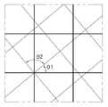
도 1a 내지 1c는 본 발명의 이해를 돕기 위한, 전도성 재료로 전극 패턴을 형성한 정전용량 방식 터치 스크린 패널의 기존 구성의 일 예를 나타낸다.
도 2a 내지 2c는 본 발명의 일 실시예에 따른, 전도성 재료로 전극 패턴을 형성한 정전용량 방식의 터치 스크린 패널의 구성을 나타낸다.
도 3a 내지 3c는 본 발명의 보다 구체적인 일 실시예에 따른 정전용량 방식의 터치 스크린 패널의 구성을 나타낸다.
도 4a는 도 1a에 도시된 연결 영역(R2)을 확대한 확대도이고, 도 4b는 도 2a에 도시된 연결 영역(R4)를 확대한 확대도이며, 도 4c는 연결 영역(R2)과 연결 영역(R4)가 중첩된 부분의 확대도이다.
도 5a는 도 3a에 도시된 연결 영역(B1')을 확대한 확대도이고, 도 5b는 도 3b에 도시된 연결 영역(B2')을 확대한 확대도이며, 도 5c는 도 3c에서 연결 영역(B1')과 연결 영역(B2')가 중첩된 부분의 확대도이다.
도 6은 본 발명의 일 실시예에 따른 격자 패턴과 화소 패턴을 나타내는 도면이다.
도 7은 도 1c의 터치 스크린 패널에서 일부 영역을 확대한 확대도이다.
도 8은 도 3c의 터치 스크린 패널에서 일부 영역을 확대한 확대도이다.
도 9는 본 발명의 실시예들에서 감지 영역에 적용될 수 있는 패턴의 예들을 나타낸다.FIGS. 1A to 1C illustrate an example of an existing configuration of a capacitive touch screen panel in which an electrode pattern is formed of a conductive material, for better understanding of the present invention.
2A to 2C show a structure of a capacitance type touch screen panel in which an electrode pattern is formed of a conductive material according to an embodiment of the present invention.
3A to 3C illustrate a configuration of a capacitive touch screen panel according to a more specific embodiment of the present invention.
FIG. 4A is an enlarged view of the connection region R2 shown in FIG. 1A; FIG. 4B is an enlarged view of the connection region R4 shown in FIG. 2A; And an enlarged view of a portion where the region R4 is superimposed.
FIG. 5A is an enlarged view of the connection area B1 'shown in FIG. 3A, FIG. 5B is an enlarged view of the connection area B2' shown in FIG. 3B, Is an enlarged view of a portion where the connection area B1 'and the connection area B2' overlap.
6 is a view showing a lattice pattern and a pixel pattern according to an embodiment of the present invention.
FIG. 7 is an enlarged view of a portion of the touch screen panel of FIG. 1C.
8 is an enlarged view of a portion of the touch screen panel of FIG. 3C.
Figure 9 shows examples of patterns that can be applied to the sensing area in embodiments of the present invention.
이하에서는 도면을 참조하여 본 발명의 바람직한 실시예들을 상세히 설명한다. 이하 설명 및 첨부된 도면들에서 실질적으로 동일한 구성요소들은 각각 동일한 부호들로 나타냄으로써 중복 설명을 생략하기로 한다. 또한 본 발명을 설명함에 있어 관련된 공지기능 혹은 구성에 대한 구체적인 설명이 본 발명의 요지를 불필요하게 흐릴 수 있다고 판단되는 경우 그에 대한 상세한 설명은 생략하기로 한다.Hereinafter, preferred embodiments of the present invention will be described in detail with reference to the drawings. In the following description and the accompanying drawings, substantially the same components are denoted by the same reference numerals, and redundant description will be omitted. In the following description of the present invention, a detailed description of known functions and configurations incorporated herein will be omitted when it may make the subject matter of the present invention rather unclear.
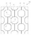
도 1a 내지 1c는 본 발명의 이해를 돕기 위한, 전도성 재료로 전극 패턴을 형성한 정전용량 방식 터치 스크린 패널의 기존 구성의 일 예를 나타낸다. 도 1a는 터치 입력의 가로축 상의 위치를 감지하기 위한 제1 센서층(10a)을, 도 1b는 터치 입력의 세로축 상의 위치를 감지하기 위한 제2 센서층(10b)을, 도 1c는 제1 센서층(10a)의 상부 또는 하부에 제2 센서층(10b)이 적층된 모습을 나타낸다.FIGS. 1A to 1C illustrate an example of an existing configuration of a capacitive touch screen panel in which an electrode pattern is formed of a conductive material, for better understanding of the present invention. 1A shows a
도 1a를 참조하면, 제1 센서층(10a)은 터치 입력의 가로축 상의 위치를 감지하기 위하여 세로 방향으로 형성되는 복수의 센서전극들(11)을 포함한다. 그리고 센서전극들(11) 각각은, 터치 스크린 패널의 표면에서의 물체(또는 사람)의 접촉을 감지하는 감지 영역들(R1)과, 감지 영역들(R1) 간을 연결하는 연결 영역들(R2)로 이루어진다.Referring to FIG. 1A, a
센서전극들(11)은 감지 영역들(R1)과 연결 영역들(R2)에 걸쳐서 일정한 두 방향의 선들이 상호 교차되는 격자 패턴으로 이루어진다. 상기 격자 패턴은 전도성 재료로 이루어지며, 예컨대 제1 센서층(10a)에 패턴이 음각으로 형성되어, 형성된 패턴에 전도성 재료가 충진되어진 형태일 수 있다.The
나아가, 제1 센서층(10a)은, 센서전극들(11)의 영역과 그 이외 영역 간의 명암 차이로 인한 시인성 열화를 방지하기 위하여, 센서전극들(11)과 전기적으로 절연되어 있으며 센서전극들(11)과 동일 또는 유사한 패턴으로 형성되지만 감지 역할을 하지 않는 더미전극들(12)을 더 포함한다. 센서전극들(11)의 패턴과 더미전극들(12)의 패턴은 연속성이 있는 것처럼 보이나, 실제로는 그 경계에서 패턴이 끊어져 있으므로 센서전극들(11)과 더미전극들(12)은 전기적으로 절연된다.The
도 1b를 참조하면, 제2 센서층(10b)은 터치 입력의 세로축 상의 위치를 감지하기 위하여 가로 방향으로 형성되는 복수의 센서전극들(13)을 포함한다. 그리고 센서전극들(13) 각각은, 터치 스크린 패널의 표면에서의 물체의 접촉을 감지하는 감지 영역들(R3)과, 감지 영역들(R3) 간을 연결하는 연결 영역들(R4)로 이루어진다.Referring to FIG. 1B, the
센서전극들(13) 역시 센서전극들(11)과 마찬가지로 감지 영역들(R3)과 연결 영역들(R4)에 걸쳐서 일정한 두 방향의 선들이 상호 교차되는 격자 패턴으로 이루어진다. 상기 격자 패턴은 전도성 재료로 이루어지며, 예컨대 제2 센서층(10b)에 패턴들이 음각으로 형성되어, 형성된 패턴에 전도성 재료가 충진되어진 형태일 수 있다.Like the
나아가, 제2 센서층(10b)은, 센서전극들(13)과 전기적으로 절연되어 있으며 센서전극들(13)과 동일 또는 유사한 패턴으로 형성되지만, 감지 역할을 하지 않는 더미전극들(14)을 더 포함한다. 센서전극들(13)의 패턴과 더미전극들(14)의 패턴은 연속성이 있는 것처럼 보이나, 실제로는 그 경계에서 패턴이 끊어져 있으므로 센서전극들(13)과 더미전극들(14)은 전기적으로 절연된다.Further, the
다만 제1 센서층(10a)의 격자 패턴과 제2 센서층(10b)의 격자 패턴은, 모아레 현상을 저감하기 위하여, 그 각도가 틀어져 있다. 즉, 제1 센서층(10a)의 격자 패턴을 형성하는 선들의 방향과 제2 센서층(10b)의 격자 패턴을 형성하는 선들의 방향은 일치하지 않는다. 모아레 현상이란, 독립된 두 개의 주기적인 패턴들이 적층될 경우에 형성되는 자연적인 간섭 현상(interference phenomenon)을 의미한다. 모아레 현상은 물결 형태의 곡선(wave), 잔물결(ripple), 작은 다발(wisp) 등의 형태로 나타난다. 제1 센서층(10a)의 격자 패턴과 제2 센서층(10b)의 격자 패턴의 각도를 틂으로써, 두 격자 패턴의 각도가 일치하는 경우보다는 모아레 현상을 어느 정도 저감시킬 수 있다.However, the grating pattern of the
도 1c는 제1 센서층(10a)과 제2 센서층(10b)이 적층된 모습을 나타낸다. 도 1c를 참조하면, 제1 센서층(10a)과 제2 센서층(10b)이 적층되는 경우 두 격자 패턴의 각도가 틀어짐으로써 모아레 현상이 어느 정도 저감되지만, 유사한 격자 패턴이 적층된 형태인 이상 모아레 현상의 극복에는 한계가 있다.FIG. 1C shows a laminated structure of the
게다가, 영상표시장치에서 터치 스크린 패널은 통상 패턴화된 화소들을 이용하여 영상을 표시하는 디스플레이 패널 위에 적층되는데, 제1 센서층(10a)의 격자 패턴과 화소 패턴의 간섭으로 인한 모아레 현상과 제2 센서층(10b)의 격자 패턴과 화소 패턴의 간섭으로 인한 모아레 현상 등 화소 패턴과의 간섭으로 인한 모아레 현상이 유발된다.In addition, in a video display device, a touch screen panel is usually stacked on a display panel that displays an image using patterned pixels. The moire phenomenon due to the interference of the lattice pattern of the
또한, 제1 센서층(10a)의 더미전극들(12)과 제2 센서층(10b)의 더미전극들(14)로 인하여 도시된 바와 같이 터치 스크린 패널의 전 영역에 걸쳐서 제1 센서층(10a)의 격자 패턴과 제2 센서층(10b)의 격자 패턴이 중첩되기 때문에 투과율이 떨어지게 된다.In addition, since the
도 2a 내지 2c는 본 발명의 일 실시예에 따른, 전도성 재료로 전극 패턴을 형성한 정전용량 방식의 터치 스크린 패널의 구성을 나타낸다. 도 2a는 터치 입력의 가로축 상의 위치를 감지하기 위한 제1 센서층(20a)을, 도 2b는 터치 입력의 세로축 상의 위치를 감지하기 위한 제2 센서층(20b)을, 도 2c는 제1 센서층(20a)의 상부 또는 하부에 제2 센서층(20b)이 적층된 모습을 나타낸다.2A to 2C show a structure of a capacitive touch screen panel in which an electrode pattern is formed of a conductive material according to an embodiment of the present invention. 2A shows a
도 2a를 참조하면, 제1 센서층(20a)은 터치 입력의 가로축 상의 위치를 감지하기 위하여 세로 방향으로 형성되는 복수의 센서전극들(21, 22, 23, 24)을 포함한다. 하나의 센서전극(22)은, 터치 스크린 패널의 표면에서 물체(또는 사람)의 접촉을 감지하는 감지 영역들(S1)과, 감지 영역들(S1) 간을 연결하는 연결 영역들(B1)로 이루어진다.Referring to FIG. 2A, the
본 실시예에서 감지 영역들(S1)은 세로 방향을 따라 지그재그로 배열되며, 연결 영역들(B1)은 이와 같이 지그재그로 배열된 감지 영역들(S1)을 연결한다. 따라서 연결 영역들(B1)이 형성하는 연결 방향 역시 지그재그로 교번하며 반복된다.In the present embodiment, the sensing areas S1 are arranged in a zigzag manner along the vertical direction, and the connection areas B1 connect the sensing areas S1 arranged in zigzags. Therefore, the connection directions formed by the connection regions B1 are alternately repeated in a staggered manner.
또한, 인접한 두 센서전극 사이에 가상의 선(세로)이 있다고 가정할 때 두 센서전극이 이 가상의 선을 중심으로 대칭을 이룬다. 예컨대, 센서전극(21)과 센서전극(22)이 대칭을 이루고, 센서전극(22)와 센서전극(23)이 대칭을 이룬다.Assuming that there is an imaginary line (vertical) between two adjacent sensor electrodes, the two sensor electrodes are symmetric about the imaginary line. For example, the
나아가, 서로 대칭을 이루는 두 센서전극들에서, 한 센서전극의 어느 하나의 감지 영역과 다른 센서전극의 어느 하나의 감지 영역은 상호 근접하게 배치되어 한 쌍을 이루고, 이렇게 한 쌍을 이루는 두 개의 감지영역은 8각형의 모양으로 형성된다. 예를 들어 도 2a를 참조하면, 센서전극(22)와 센서전극(23)에서, 센서전극(22)의 한 감지 영역(위쪽의 S1)과 그 오른편에 근접한 센서전극(23)의 감지 영역이 한 쌍을 이루고, 이 쌍을 이루는 두 개의 감지 영역은 도시된 바와 같이 8각형의 모양으로 형성된다. 다만 이렇게 한 쌍을 이루는 두 개의 감지영역은 서로 다른 센서전극 상에 있으므로 서로 절연되어 있다. 또한, 센서전극(21)과 센서전극(22)에서, 센서전극(22)의 한 감지 영역(아래쪽의 S1)과 그 왼편에 근접한 센서전극(21)의 감지 영역이 한 쌍을 이루고, 이 쌍을 이루는 두 개의 감지 영역 역시 도시된 바와 같이 8각형의 모양으로 형성된다.Further, in two sensor electrodes symmetrical to each other, one of the sensing areas of one sensor electrode and one of the sensing electrodes of the other sensor electrode are arranged close to each other to form a pair, The region is formed in an octagonal shape. 2A, a sensing region of the sensor electrode 22 (upper portion S1) and a sensing region of the
감지 영역들(S1)과 연결 영역들(B1)은, 도시되지는 않았으나 소정의 전극 패턴으로 이루어진다. 소정의 전극 패턴은 전도성 재료로 이루어지며, 예컨대 제1 센서층(20a)에 소정 패턴이 음각으로 형성되어, 형성된 패턴에 전도성 재료가 충진되어진 형태일 수 있다.The sensing areas S1 and the connection areas B1 are made of a predetermined electrode pattern though not shown. The predetermined electrode pattern is made of a conductive material, for example, a predetermined pattern may be formed in the
도 2a에서는 편의상 센서전극들(21, 22, 23, 24) 각각의 외곽선이 도시되어 있는데, 외곽선은 패턴의 일부로서 또는 패턴과 별도로 존재할 수도 있으나, 도시된 외곽선은 실제로 존재하지 않고 패턴이 형성된 영역과 패턴이 형성되지 않은 영역의 경계일 수 있다.In FIG. 2A, for the sake of convenience, the outline of each of the
또한, 도 2a를 참조하면, 센서전극들(21, 22, 23, 24)의 영역 이외의 영역에 예컨대 도 1a의 더미전극들(12)과 같은 전극 패턴은 존재하지 않는다.2A, there is no electrode pattern such as the
도 2b를 참조하면, 제2 센서층(20b)은 터치 입력의 세로축 상의 위치를 감지하기 위하여 가로 방향으로 형성되는 복수의 센서전극들(25, 26, 27, 28)을 포함한다. 하나의 센서전극(26)은, 터치 스크린 패널의 표면에서 물체의 접촉을 감지하는 감지 영역들(S2)과, 감지 영역들(S2) 간을 연결하는 연결 영역들(B2)로 이루어진다.Referring to FIG. 2B, the
본 실시예에서 감지 영역들(S2)은 가로 방향을 따라 지그재그로 배열되며, 연결 영역들(B2)은 이와 같이 지그재그로 배열된 감지 영역들(S2) 간을 연결한다. 따라서 연결 영역들(B2)이 형성하는 연결 방향 역시 지그재그로 교번하며 반복된다.In this embodiment, the sensing areas S2 are arranged in a zigzag manner along the horizontal direction, and the connection areas B2 connect the sensing areas S2 arranged in zigzags. Therefore, the connection directions formed by the connection regions B2 are repeated alternately in a staggered manner.
또한, 인접한 두 센서전극 사이에 가상의 선(가로)이 있다고 가정할 때, 두 센서전극이 이 가상의 선을 중심으로 대칭을 이룬다. 예컨대, 센서전극(25)와 센서전극(26)이 대칭을 이루고, 센서전극(26)과 센서전극(27)이 대칭을 이룬다.Assuming that there is an imaginary line (horizontal) between two adjacent sensor electrodes, the two sensor electrodes are symmetric about the imaginary line. For example, the
나아가, 서로 대칭을 이루는 두 센서전극들에서, 한 센서전극의 어느 하나의 감지 영역과 다른 센서전극의 어느 하나의 감지 영역은 상호 근접하게 배치되어 한 쌍을 이루고, 이렇게 한 쌍을 이루는 두 개의 감지영역은 8각형의 모양으로 형성된다. 예를 들어 도 2b를 참조하면, 센서전극(25)와 센서전극(26)에서, 센서전극(26)의 한 감지 영역(왼쪽의 S2)과 그 위편에 근접한 센서전극(25)의 감지 영역이 한 쌍을 이루고, 이 쌍을 이루는 두 개의 감지 영역은 도시된 바와 같이 8각형의 모양으로 형성된다. 다만 이렇게 한 쌍을 이루는 두 개의 감지영역은 서로 다른 센서전극 상에 있으므로 서로 절연되어 있다. 또한, 센서전극(26)과 센서전극(27)에서, 센서전극(26)의 한 감지 영역(오른쪽의 S2)과 그 아래편에 근접한 센서전극(27)의 감지 영역이 한 쌍을 이루고, 이 쌍을 이루는 두 개의 감지 영역 역시 도시된 바와 같이 8각형의 모양으로 형성된다.Further, in two sensor electrodes symmetrical to each other, one of the sensing areas of one sensor electrode and one of the sensing electrodes of the other sensor electrode are arranged close to each other to form a pair, The region is formed in an octagonal shape. For example, referring to FIG. 2B, in the
감지 영역들(S2)과 연결 영역들(B2)은, 도시되지는 않았으나 소정의 전극 패턴으로 이루어진다. 도 2b에서는 편의상 센서전극들(25, 26, 27, 28) 각각의 외곽선이 도시되어 있는데, 외곽선은 패턴의 일부로서 또는 패턴과 별도로 존재할 수도 있으나, 도시된 외곽선은 실제로 존재하지 않고 패턴이 형성된 영역과 패턴이 형성되지 않은 영역의 경계일 수 있다.The sensing areas S2 and connection areas B2 are formed of a predetermined electrode pattern though not shown. In FIG. 2B, the outline of each of the
또한, 도 2b를 참조하면, 센서전극들(25, 26, 27, 28)의 영역 이외의 영역에 예컨대 도 1b의 더미전극들(14)과 같은 전극 패턴은 존재하지 않는다.2B, there is no electrode pattern such as the
도 2c는 제1 센서층(20a)과 제2 센서층(20b)이 적층된 모습을 나타낸다. 도 2c를 참조하면, 터치 스크린 패널을 적층 방향에서 볼 때, 즉 터치 스크린 패널을 상방 또는 하방에서 볼 때 제1 센서층(20a)의 감지 영역(S1)과 제2 센서층(20b)의 감지 영역(S2)는 중첩되지 않는다. 즉, 터치 스크린 패널을 적층 방향에서 볼 때, 제1 센서층(20a)의 감지 영역(S1)은 제2 센서층(20b)의 센서전극 영역 이외의 영역에 놓이며, 제2 센서층(20b)의 감지 영역(S2)은 제1 센서층(20a)의 센서전극 영역 이외의 영역에 놓인다.FIG. 2C shows a laminated structure of the
그러나, 터치 스크린 패널을 적층 방향에서 볼 때 제1 센서층(20a)의 연결 영역(B1)과 제2 센서층(20b)의 대응하는 연결 영역(B2)은 서로 중첩된다.However, when the touch screen panel is viewed in the laminating direction, the connection area B1 of the
모아레 현상을 최소화하고 투과율을 높이기 위해서는, 터치 스크린 패널을 적층 방향에서 볼 때, 3차원적으로는 전극 패턴의 일부와 다른 일부가 별개의 층에 형성되더라도, 2차원적으로 전극 패턴이 하나의 층으로 보이는 것이 바람직하다.In order to minimize the moiré phenomenon and increase the transmittance, it is necessary that the electrode pattern is formed in one layer two-dimensionally even if a part of the electrode pattern and another part of the electrode pattern are formed in different layers when viewed from the lamination direction of the touch screen panel. .
따라서 위와 같이 제1 센서층(20a)의 감지 영역(S1)과 제2 센서층(20b)의 감지 영역(S2)이 중첩되지 않고 제1 센서층(20a)의 연결 영역(B1)과 제2 센서층(20b)의 대응하는 연결 영역(B2)이 서로 중첩될 때, 감지 영역(S1)과 감지 영역(S2)은 동일 또는 유사한 패턴으로 형성하고, 연결 영역(B1)과 연결 영역(B2)은 감지 영역(S1, S2)과는 다른 패턴으로서 서로 중첩될 경우 감지 영역(S1, S2)과 동일 또는 유사한 패턴을 띠도록 패턴을 형성하면, 2차원적으로 전극 패턴이 하나의 층으로 보이도록 할 수 있다.The sensing area S1 of the
예컨대, 감지 영역(S1, S2)의 전극 패턴이 특정 패턴인 경우, 그 특정 패턴의 일부를 연결 영역(B1)의 패턴으로 결정하고, 그 특정 패턴의 나머지 일부를 연결 영역(B2)의 패턴으로 결정한다면, 연결 영역(B1)과 연결 영역(B2)이 서로 중첩될 경우 감지 영역(S1, S2)과 동일 또는 유사한 패턴을 띠도록 할 수 있다.For example, when the electrode pattern of the sensing area S1 or S2 is a specific pattern, a part of the specific pattern is determined as a pattern of the connection area B1, and the remaining part of the specific pattern is patterned as a pattern of the connection area B2 If the connection area B1 and the connection area B2 are overlapped with each other, they may have the same or similar pattern as the sensing areas S1 and S2.
구체적으로 본 발명의 일 실시예에서, 감지 영역(S1, S2)의 전극 패턴을 격자 패턴으로 형성하고, 그 격자 패턴을 이루는 일 방향의 직선 패턴을 연결 영역(B1)의 패턴으로 형성하고, 그 격자 패턴을 이루는 다른 방향의 직선 패턴을 연결 영역(B2)의 패턴으로 형성할 수 있다.Specifically, in one embodiment of the present invention, the electrode patterns of the sensing areas S1 and S2 are formed in a lattice pattern, a linear pattern in one direction forming the lattice pattern is formed in the pattern of the connection area B1, It is possible to form the linear pattern of the other direction forming the lattice pattern in the pattern of the connection region B2.
도 3a 내지 3c는 이러한 본 발명의 보다 구체적인 일 실시예에 따른 정전용량 방식의 터치 스크린 패널의 구성을 나타낸다. 도 3a는 터치 입력의 가로축 상의 위치를 감지하기 위한 제1 센서층(20a')을, 도 3b는 터치 입력의 세로축 상의 위치를 감지하기 위한 제2 센서층(20b')을, 도 3c는 제1 센서층(20a')의 상부 또는 하부에 제2 센서층(20b')이 적층된 모습을 나타낸다. 본 실시예에 따른 정전용량 방식의 터치 스크린 패널은 도 2a 내지 도 2c를 통하여 설명한 실시예의 특징들을 모두 포함하므로, 중복되는 설명은 생략하고 추가적인 특징들만 설명한다.3A to 3C illustrate a configuration of a capacitive touch screen panel according to a more specific embodiment of the present invention. FIG. 3A shows a
도 3a를 참조하면, 센서전극(22')에서, 감지 영역들(S1')의 전극 패턴은 격자 패턴으로 이루어지고, 감지 영역들(S1') 간을 연결하는 연결 영역들(B1')의 전극 패턴은 서로 평행한 복수의 직선들을 포함하는 직선 패턴으로 이루어진다.Referring to FIG. 3A, in the sensor electrode 22 ', the electrode patterns of the sensing areas S1' are formed in a lattice pattern, and the connection areas B1 'connecting the sensing areas S1' The electrode pattern is made of a linear pattern including a plurality of straight lines which are parallel to each other.
격자 패턴은 일정한 두 방향의 선들이 상호 교차되는 형태의 패턴인 바, 연결 영역들(B1')의 직선 패턴을 이루는 직선들의 방향은 격자 패턴을 이루는 직선의 일 방향과 일치하며, 또한 연결되는 두 감지 영역의 연결 방향과 일치한다. 따라서 도시된 바와 같이 연결 영역들(B1')의 직선 패턴을 이루는 직선들의 방향은 지그재그로 교번하며 반복된다.The grid pattern is a pattern in which lines of two directions are mutually intersected. The direction of the straight lines forming the linear pattern of the connection areas B1 'coincides with one direction of the straight line forming the grid pattern, And coincides with the connection direction of the sensing area. Therefore, as shown in the figure, the directions of the straight lines forming the linear pattern of the connection areas B1 'are repeated alternately in a zigzag manner.
도 3b를 참조하면, 센서전극(26')에서, 감지 영역들(S2')의 전극 패턴은 감지 영역들(S1')과 동일 또는 유사한 격자 패턴으로 이루어지고, 감지 영역들(S2') 간을 연결하는 연결 영역들(B2')의 전극 패턴은 서로 평행한 복수의 직선들을 포함하는 직선 패턴으로 이루어진다.Referring to FIG. 3B, in the sensor electrode 26 ', the electrode patterns of the sensing areas S2' are formed in the same or similar lattice pattern as the sensing areas S1 ' The electrode patterns of the connection regions B2 'connecting the first and second electrode layers are formed in a linear pattern including a plurality of straight lines parallel to each other.
도 3a와 마찬가지로, 연결 영역들(B2')의 직선 패턴을 이루는 직선들의 방향은 격자 패턴을 이루는 직선의 일 방향과 일치하며, 또한 연결되는 두 감지 영역의 연결 방향과 일치한다. 따라서 도시된 바와 같이 연결 영역들(B2')의 직선 패턴을 이루는 직선들의 방향은 지그재그로 교번하며 반복된다.3A, the directions of the straight lines forming the linear patterns of the connection regions B2 'coincide with one direction of the straight line forming the lattice pattern, and coincide with the connection directions of the two sensing regions to be connected. Therefore, as shown in the figure, the directions of the straight lines forming the linear pattern of the connection regions B2 'are alternately repeated in a zigzag manner.
도 3c는 제1 센서층(20a')과 제2 센서층(20b')이 적층된 모습을 나타낸다. 도 3c를 참조하면, 터치 스크린 패널을 적층 방향에서 볼 때 제1 센서층(20a')의 감지 영역들(S1')의 격자 패턴과 제2 센서층(20b')의 감지 영역들(S2')의 격자 패턴은 중첩되지 않는다. 그러나 터치 스크린 패널을 적층 방향에서 볼 때 제1 센서층(20a')의 연결 영역(B1')과 제2 센서층(20b')의 대응하는 연결 영역(B2')은 서로 중첩되고, 중첩된 연결 영역(B1')과 연결 영역(B2')은 감지 영역들(S1', S2')과 동일 또는 유사한 형태의 격자 패턴을 형성한다. 즉, 연결 영역(B1')의 직선 패턴과 연결 영역(B2')의 직선 패턴은 서로 다른 방향의 직선들로 이루어지므로, 두 직선 패턴이 중첩되면 격자 패턴을 형성하게 된다.FIG. 3C shows a laminated structure of the
본 발명의 실시예에 따르면, 터치 스크린 패널을 적층 방향에서 볼 때 제1 센서층(20a')의 감지 영역들(S1')과 제2 센서층(20b')의 감지 영역들(S2') 중 어떤 부분에서도 오직 한 층의 격자 패턴이 형성된다. 또한, 제1 센서층(20a')의 연결 영역(B1')과 제2 센서층(20b')의 연결 영역(B2')이 중첩된 부분은 감지 영역들(S1') 또는 감지 영역들(S2')의 격자 패턴과 연속성을 띠게 된다. 결국 터치 스크린 패널을 적층 방향에서 볼 때 전체적으로 단일하고 연속적인 격자 패턴이 형성된 것으로 보여지고, 감지 영역들(S1', S2')과 연결 영역들(B1', B2')의 명암 차이가 발생하지 않으므로 투과율과 시인성이 향상된다. 또한 제1 센서층(20a')의 패턴과 제2 센서층(20b')의 패턴 간의 간섭이 거의 없기 때문에 모아레 현상이 최소화될 수 있다.According to an embodiment of the present invention, the sensing areas S1 'of the
나아가, 본 발명의 실시예에 의하면, 제1 센서층(20a')의 전극 패턴과 제2 센서층(20b')의 전극 패턴을 동일하게 할 수 있다. 예컨대 도 3a와 도 3b를 비교하여 보면, 도 3a의 패턴을 90도 회전하면 도 3b의 패턴과 일치한다. 따라서 합치 공차가 줄어들고 전극 패턴을 형성하기 위한 몰드를 하나로 사용하여 패턴 제작이 가능한 등 제작 공정상의 이점 또한 존재한다.Furthermore, according to the embodiment of the present invention, the electrode pattern of the
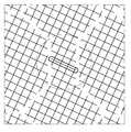
도 4a는 도 1a에 도시된 연결 영역(R2)을 확대한 확대도이고, 도 4b는 도 2a에 도시된 연결 영역(R4)를 확대한 확대도이며, 도 4c는 연결 영역(R2)과 연결 영역(R4)가 중첩된 부분의 확대도이다.FIG. 4A is an enlarged view of the connection region R2 shown in FIG. 1A; FIG. 4B is an enlarged view of the connection region R4 shown in FIG. 2A; And an enlarged view of a portion where the region R4 is superimposed.
도 4a 또는 도 4b를 참조하면, 연결 영역(R2, R4)을 이루는 패턴 중 일부분이 탈락되거나 단선되면 감지 영역 간의 전기적 연결이 끊어지는 문제가 발생할 수 있다. 예컨대, 도 4a 또는 도 4b에 표시된 라인에 탈락 또는 단선이 발생하는 경우 감지 영역 간의 전기적 연결은 끊어지게 된다. 혹은, 도 4a 또는 도 4b에 표시된 라인 중 각각 한 라인에 탈락 또는 단선이 발생하는 경우, 감지 영역들 간이 병렬이 아닌 직렬로 연결되어 전체 저항이 증가하게 된다.Referring to FIG. 4A or FIG. 4B, when a part of the patterns forming the connection regions R2 and R4 are disconnected or disconnected, the electrical connection between the sensing regions may be interrupted. For example, when the line shown in FIG. 4A or 4B is dropped or broken, the electrical connection between the sensing areas is cut off. 4A or 4B, the sensing regions are connected in series rather than in parallel, so that the total resistance is increased.
또한, 도 4a 및 도 4b를 참조하면, 감지 영역과 연결 영역의 패턴 모양이 동일하게 형성된다. 이때, 연결 영역의 길이 방향과 연결 영역을 이루는 라인의 방향이 동일하지 않기 때문에, 연결 영역에서 실질적으로 신호를 전달하는 라인이 부분적으로 3개의 라인에서 2개의 라인으로 감소하게 되는데, 이와 같은 라인 개수가 감소하는 구간에서 탈선 또는 단선이 발생하면 위와 같이 신호 전달이 안 되거나 전체 저항이 증가하는 문제가 발생하게 된다.4A and 4B, the pattern shapes of the sensing area and the connection area are formed to be the same. At this time, since the longitudinal direction of the connection area and the direction of the line constituting the connection area are not the same, a line substantially conveying a signal in the connection area is partially reduced from three lines to two lines, If a derailment or disconnection occurs in a section where the voltage is reduced, signal transmission may not be performed or the total resistance may increase.
또한, 도 4c를 참조하면, 연결 영역(R2)의 격자 패턴과 연결 영역(R4)의 격자 패턴이 중첩됨으로 인하여, 연결 영역 부분에서의 패턴의 간섭으로 인한 모아레 현상의 발생과 투과율의 저하가 불가피하다.Referring to FIG. 4C, since the grid pattern of the connection region R2 overlaps with the grid pattern of the connection region R4, it is inevitable that the occurrence of the moire phenomenon and the decrease of the transmittance due to the interference of the pattern in the connection region portion are inevitable Do.
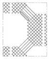
도 5a는 도 3a에 도시된 연결 영역(B1')을 확대한 확대도이고, 도 5b는 도 3b에 도시된 연결 영역(B2')을 확대한 확대도이며, 도 5c는 도 3c에서 연결 영역(B1')과 연결 영역(B2')가 중첩된 부분의 확대도이다.FIG. 5A is an enlarged view of the connection area B1 'shown in FIG. 3A, FIG. 5B is an enlarged view of the connection area B2' shown in FIG. 3B, Is an enlarged view of a portion where the connection area B1 'and the connection area B2' overlap.
도 5a 또는 도 5b를 참조하면, 연결 영역(B1', B2')을 이루는 직선 패턴의 방향과 연결 영역(B1', B2')의 길이 방향이 동일하기 때문에 안정적으로 적어도 3개의 직선 패턴(라인)이 형성되는 것을 확인할 수 있다. 본 발명의 실시예에 의하면, 센서층 내에서 연결 영역(B1', B2')이 차지하는 영역은 제한적(연결 영역이 차지하는 영역은 감지 능력을 위해 감지 영역이 차지하는 최소 면적에 의해 결정됨)인데, 이 제한적인 영역 내에서 신호의 간섭, 저항, 신호의 전달 안정성 등을 고려한 결과 3~5개의 직선 패턴이 보다 효과적이다. 만약, 연결 영역(B1', B2')을 이루는 직선 패턴 중 하나가 탈락되거나 단선되더라도, 모든 직선이 탈락되거나 단선되지 않는 한 감지 영역 간의 전기적 연결은 끊어지지 않는다. 예컨대, 도 5a에 표시된 라인에 탈락 또는 단선이 발생하더라도 감지 영역 간의 전기적 연결은 끊어지지 않는다. 즉, 감지 영역 간을 연결하는 연결 영역(B1', B2')이 적어도 3개의 직선들로 이루어지는 직선 패턴으로 형성되므로, 일부 직선에서 탈락 또는 단선이 발생하더라도 감지 영역 간의 전기적 연결은 끊어지지 않는다.5A or 5B, since the direction of the linear pattern constituting the connection regions B1 'and B2' is the same as the longitudinal direction of the connection regions B1 'and B2', at least three linear patterns ) Is formed. According to the embodiment of the present invention, the area occupied by the connection areas B1 ', B2' in the sensor layer is limited (the area occupied by the connection area is determined by the minimum area occupied by the sensing area for sensing capability) Considering signal interference, resistance and signal transmission stability within the limited area, 3 to 5 linear patterns are more effective. Even if one of the linear patterns constituting the connection areas B1 'and B2' is disconnected or disconnected, the electrical connection between the sensing areas is not interrupted unless all the straight lines are disconnected or disconnected. For example, even if a line shown in FIG. 5A is dropped or broken, the electrical connection between the sensing areas is not cut off. That is, since the connection regions B1 'and B2' connecting the sensing regions are formed in a linear pattern composed of at least three straight lines, the electrical connection between the sensing regions is not cut off even if some straight lines are disconnected or broken.
또한, 도 5c를 참조하면, 연결 영역(B1')의 직선 패턴과 연결 영역(B2')의 직선 패턴이 중첩되어 단일한 격자 패턴을 형성하므로, 모아레 현상이 저감되고 투과율 또한 향상됨을 알 수 있다.5C, it can be seen that the linear pattern of the connection area B1 'and the linear pattern of the connection area B2' are overlapped to form a single lattice pattern, so that the moire phenomenon is reduced and the transmittance is also improved .
또한, 전술한 바와 같이 터치 스크린 패널은 통상 패턴화된 화소들을 이용하여 영상을 표시하는 디스플레이 패널 위에 적층되고, 화소 패턴은 가로 및 세로 방향으로 형성된다. 그리고 이러한 화소 패턴의 방향과 터치 스크린 패널의 패턴의 방향이 유사할수록 화소 패턴과의 간섭으로 인한 모아레 현상이 더욱 심각해질 수 있다.Also, as described above, the touch screen panel is usually stacked on a display panel that displays an image using patterned pixels, and pixel patterns are formed in the horizontal and vertical directions. As the direction of the pixel pattern and the direction of the pattern of the touch screen panel are similar to each other, the moire phenomenon due to interference with the pixel pattern may become more serious.
그런데 본 발명의 실시예에 의하면, 터치 스크린 패널의 격자 패턴(제1 센서층의 패턴과 제2 센서층의 패턴이 적층되어 형성되는 격자 패턴)을 이루는 직선의 방향은 화소 패턴, 즉 화소 매트릭스와 일정 각만큼 틀어져(tilting) 있기 때문에 모아레 현상이 감소한다. 도 6은 본 발명의 일 실시예에 따른 격자 패턴과 가로 및 세로 방향의 화소 패턴을 나타내는 도면이다. 도 6을 참조하면, 격자 패턴(도시된 격자 패턴은, 제1 센서층 내 감지 영역의 격자 패턴이거나, 혹은 제2 센서층 내 감지 영역의 격자 패턴이거나, 혹은 제1 센서층의 연결 영역과 제2 센서층의 연결 영역이 중첩됨으로써 형성된 격자 패턴일 수 있음)의 일 직선의 방향(혹은, 직선 패턴을 이루는 직선의 방향)은 화소 매트릭스의 일 방향과 θ1만큼 틀어져 있고, 격자 패턴의 내각(격자 패턴에서 서로 교차하는 두 직선이 이루는 각)은 θ2이다. 여기서 θ1은 예컨대 30°~60°일 수 있고, θ2는 예컨대 60°~120°일 수 있다. 보다 바람직하게는, θ1은 35°~55°, θ2는 82°~98°일 수 있다. θ1과 θ2의 이러한 범위 내에서 모아레 현상은 더욱 방지될 수 있다.However, according to the embodiment of the present invention, the direction of the straight line forming the grid pattern of the touch screen panel (the grid pattern in which the pattern of the first sensor layer and the pattern of the second sensor layer are laminated) The Moiré phenomenon is reduced because it is tilted by a certain angle. 6 is a view showing a lattice pattern and pixel patterns in the horizontal and vertical directions according to an embodiment of the present invention. Referring to FIG. 6, the grid pattern (the grid pattern shown is a grid pattern of the sensing area in the first sensor layer, a grid pattern of the sensing area in the second sensor layer, (Or the direction of a straight line forming a linear pattern) of the grid pattern may be a grid pattern formed by superimposing the connection regions of the two sensor layers) is angled with respect to one direction of the pixel matrix by?1 , The angle formed by two straight lines intersecting each other in the lattice pattern) is?2 . Here,?1 may be, for example, 30 to 60, and?2 may be 60 to 120, for example. More preferably, &thetas;1 may be 35 DEG to 55 DEG, and &thetas;2 may be 82 DEG to 98 DEG. Within this range of?1 and?2 , the moire phenomenon can be further prevented.
도 7은 도 1c의 터치 스크린 패널에서 일부 영역을 확대한 확대도이다. 도시된 바와 같이, 감지 영역(R1, R3)의 격자 패턴과 더미 전극(14, 12)의 격자 패턴이 중첩되거나, 연결 영역(R2)과 연결 영역(R4)의 격자 패턴이 중첩됨으로 인하여, 투과율과 시인성이 저하된다.FIG. 7 is an enlarged view of a portion of the touch screen panel of FIG. 1C. As shown in the figure, since the grid pattern of the sensing regions R1 and R3 overlaps with the grid pattern of the
도 8은 도 3c의 터치 스크린 패널에서 일부 영역을 확대한 확대도이다. 도시된 바와 같이, 더미 전극 없이 감지 영역(S1') 또는 감지 영역(S2') 중 어느 하나의 격자 패턴만이 존재하거나, 연결 영역(B1')과 연결 영역(B2')이 중첩되더라도 2차원적으로는 하나의 격자 패턴만이 존재하므로, 투과율과 시인성이 향상된다.8 is an enlarged view of a portion of the touch screen panel of FIG. 3C. As shown in the figure, even if there is only one grid pattern of the sensing area S1 'or the sensing area S2' without a dummy electrode, or even if the connection area B1 'and the connection area B2' overlap each other, Since there is only one grid pattern, transmittance and visibility are improved.
투과율 또는 시인성의 지표가 되는 개구율은 일정 기준 면적에서 선면적이 차지하지 않는 투과면적의 비율과 선면적의 비율로 정의되는데, 도 8의 개구율은 도 7의 개구율보다 큰 값을 가진다. 예컨대, 도 7의 경우 개구율은 92%로 나타나고, 도 8의 경우 개구율은 98.3%로 나타난다.The aperture ratio, which is an index of transmittance or visibility, is defined as the ratio of the area of the transmissive area and the area of the linear area that does not occupy the line area at a certain reference area. The aperture ratio in FIG. 8 is larger than the aperture ratio in FIG. For example, in FIG. 7, the aperture ratio is 92%, and in FIG. 8, the aperture ratio is 98.3%.
본 발명의 실시예들에서, 감지 영역 또는 연결 영역을 이루는 패턴의 선폭은 예컨대 1~9μm 일 수 있고, 선들 간의 간격으로 정의되는 피치(pitch)는 예컨대 300~700μm 일 수 있다. 또한, 연결 영역의 길이(즉, 하나의 센서전극에서 인접한 감지 영역 간의 이격 거리)는 예컨대 1.5~2mm 일 수 있고, 동일선상에서 감지 영역 간의 이격 거리는 예컨대 3~9mm 일 수 있다. 또한 연결 영역의 직선 패턴을 이루는 직선의 개수는, 신호 전달 효율과 공정 결함을 고려하여 적절하게 결정될 수 있는데, 예컨대 3 내지 5개일 수 있다.In embodiments of the present invention, the line width of the pattern constituting the sensing area or the connecting area may be, for example, 1 to 9 μm, and the pitch defined by the interval between the lines may be, for example, 300 to 700 μm. In addition, the length of the connection area (i.e., the distance between adjacent sensing areas in one sensor electrode) may be, for example, 1.5 to 2 mm, and the distance between sensing areas on the same line may be, for example, 3 to 9 mm. Also, the number of straight lines constituting the linear pattern of the connection area can be appropriately determined in consideration of signal transmission efficiency and process defects, for example, from 3 to 5.
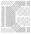
도 9는 본 발명의 실시예들에서 감지 영역에 적용될 수 있는 패턴의 예들을 나타낸다. 감지 영역에 적용될 수 있는 패턴은 도시된 바와 같이, 정사각 격자 패턴, 마름모 격자 패턴, 파도형 격자 패턴, 십자형 패턴, 테트리스 패턴(테트리스 도형들이 결합된 형태의 패턴) 중 하나일 수 있다. 감지 영역을 위한 패턴이 특정 패턴으로 결정되면, 연결 영역을 위한 패턴은 그 특정 패턴의 일부로 결정될 수 있다. 즉, 특정 패턴에 포함된 일부 패턴이 한 센서층의 연결 영역을 위한 패턴이 되고, 특정 패턴에 포함된 나머지 일부 패턴이 다른 센서층의 연결 영역을 위한 패턴이 되어, 두 패턴이 중첩되면 특정 패턴을 형성하도록 연결 영역을 위한 패턴이 결정될 수 있다. 예컨대 전술한 실시예들에서처럼, 감지 영역을 위한 패턴이 격자 패턴인 경우, 중첩될 연결 영역들을 위한 패턴은 서로 다른 방향의 직선 패턴들로 결정될 수 있다.Figure 9 shows examples of patterns that can be applied to the sensing area in embodiments of the present invention. The pattern that can be applied to the sensing region may be one of a square-shaped grid pattern, a rhombic grid pattern, a wave-like grid pattern, a cross pattern, a Tetris pattern (a pattern in which Tetris patterns are combined) as shown. If the pattern for the sensing area is determined as a specific pattern, the pattern for the connecting area can be determined as a part of the specific pattern. That is, some patterns included in a specific pattern become patterns for a connection region of one sensor layer, and some remaining patterns included in the specific pattern become patterns for connection regions of different sensor layers. When two patterns are overlapped, The pattern for the connection area can be determined. For example, as in the above-described embodiments, when the pattern for the sensing area is a lattice pattern, the pattern for the connecting areas to be overlapped can be determined as linear patterns in different directions.
이제까지 본 발명에 대하여 그 바람직한 실시예들을 중심으로 살펴보았다. 본 발명이 속하는 기술 분야에서 통상의 지식을 가진 자는 본 발명이 본 발명의 본질적인 특성에서 벗어나지 않는 범위에서 변형된 형태로 구현될 수 있음을 이해할 수 있을 것이다. 그러므로 개시된 실시예들은 한정적인 관점이 아니라 설명적인 관점에서 고려되어야 한다. 예컨대, 본 발명의 실시예들에서 센서전극들의 패턴은 센서층에 음각으로 형성되어, 형성된 패턴에 전도성 재료가 충진되어진 형태로 설명하였으나, 센서전극들의 패턴은 센서층에 양각으로 형성될 수도 있다.The present invention has been described with reference to the preferred embodiments. It will be understood by those skilled in the art that various changes in form and details may be made therein without departing from the spirit and scope of the invention as defined by the appended claims. Therefore, the disclosed embodiments should be considered in an illustrative rather than a restrictive sense. For example, in the embodiments of the present invention, the pattern of the sensor electrodes is formed in the sensor layer at a negative angle, and the pattern formed is filled with the conductive material. However, the pattern of the sensor electrodes may be formed in the sensor layer in a boss.
본 발명의 범위는 전술한 설명이 아니라 특허청구범위에 나타나 있으며, 그와 동등한 범위 내에 있는 모든 차이점은 본 발명에 포함된 것으로 해석되어야 할 것이다.The scope of the present invention is defined by the appended claims rather than by the foregoing description, and all differences within the scope of equivalents thereof should be construed as being included in the present invention.
Claims (33)
Translated fromKorean상기 제1 센서층의 상부 또는 하부에 적층되며, 상기 터치 입력의 다른 축 상의 위치를 감지하기 위한 복수의 제2 센서전극들을 포함하는 제2 센서층을 포함하며,
상기 제1 센서전극들 각각은 제1 방향을 따라 지그재그로 배열되는 제1 감지 영역들 및 제1 감지 영역들 간을 연결하는 제1 연결 영역들로 이루어지고,
상기 제2 센서전극들 각각은 제2 방향을 따라 지그재그로 배열되는 제2 감지 영역들 및 제2 감지 영역들 간을 연결하는 제2 연결 영역들로 이루어지는 것을 특징으로 하는 터치 스크린 패널.A first sensor layer including a plurality of first sensor electrodes for sensing a position on an axis of the touch input; And
And a second sensor layer stacked on or under the first sensor layer and including a plurality of second sensor electrodes for sensing a position on the other axis of the touch input,
Each of the first sensor electrodes includes first sensing regions arranged in a zigzag manner along a first direction and first connection regions connecting the first sensing regions,
Wherein each of the second sensor electrodes comprises second sensing regions arranged in a zigzag manner along a second direction, and second connection regions connecting the second sensing regions.
상기 제1 또는 제2 감지 영역들의 전극 패턴과 상기 제1 또는 제2 연결 영역들의 전극 패턴은 상이한 형태의 패턴인 것을 특징으로 하는 터치 스크린 패널.The method according to claim 1,
Wherein the electrode patterns of the first or second sensing regions and the electrode patterns of the first or second connection regions are patterns of different types.
상기 제1 감지 영역들과 상기 제2 감지 영역들은 중첩되지 않는 것을 특징으로 하는 터치 스크린 패널.The method according to claim 1,
Wherein the first sensing areas and the second sensing areas do not overlap.
상기 제1 연결 영역들과 상기 제2 연결 영역들은 적어도 일부 중첩되는 것을 특징으로 하는 터치 스크린 패널.The method according to claim 1,
Wherein the first connection regions and the second connection regions overlap at least partially.
상기 제1 감지 영역들의 전극 패턴과 상기 제2 감지 영역들의 전극 패턴은 동일한 형태의 패턴인 것을 특징으로 하는 정전용량 방식의 터치 스크린 패널.The method according to claim 1,
Wherein the electrode pattern of the first sensing regions and the electrode pattern of the second sensing regions are the same pattern.
상기 제1 감지 영역들의 전극 패턴과 상기 제2 감지 영역들의 전극 패턴은 동일한 형태의 패턴이고,
상기 제1 및 제2 연결 영역들의 전극 패턴은 상기 제1 및 제2 감지 영역들의 전극 패턴과 상이한 형태의 패턴이며,
상기 제1 연결 영역들과 상기 제2 연결 영역들은 적어도 일부 중첩되고,
상기 제1 연결 영역들과 상기 제2 연결 영역들이 중첩된 영역의 패턴은 상기 제1 및 제2 감지 영역들의 전극 패턴과 동일한 형태의 패턴인 것을 특징으로 하는 터치 스크린 패널.The method according to claim 1,
The electrode patterns of the first sensing regions and the electrode patterns of the second sensing regions have the same pattern,
The electrode patterns of the first and second connection regions are patterns different from the electrode patterns of the first and second sensing regions,
Wherein the first connection regions and the second connection regions are at least partially overlapped,
Wherein the pattern of the region in which the first connection regions and the second connection regions are overlapped is the same pattern as the electrode patterns of the first and second sensing regions.
상기 제1 및 제2 감지 영역들의 전극 패턴은 격자 패턴으로 이루어지고, 상기 제1 및 제2 연결 영역들의 전극 패턴은 직선 패턴으로 이루어지는 것을 특징으로 하는 터치 스크린 패널.The method according to claim 1,
Wherein the electrode patterns of the first and second sensing regions are in a lattice pattern, and the electrode patterns of the first and second connection regions are in a linear pattern.
상기 직선 패턴을 이루는 직선의 방향은 상기 격자 패턴을 이루는 직선의 일 방향과 일치하는 것을 특징으로 하는 터치 스크린 패널.8. The method of claim 7,
Wherein the direction of the straight line forming the straight line pattern coincides with one direction of the straight line forming the grid pattern.
상기 제1 감지 영역들의 격자 패턴과 상기 제2 감지 영역들의 격자 패턴은 중첩되지 않는 것을 특징으로 하는 터치 스크린 패널.8. The method of claim 7,
Wherein the grid pattern of the first sensing regions and the grid pattern of the second sensing regions do not overlap.
상기 제1 및 제2 감지 영역들의 전극 패턴의 격자 패턴을 이루는 적어도 하나의 직선 패턴과 상기 제1 또는 제2 연결 영역들의 전극 패턴의 직선 패턴은 서로 평행하거나,
상기 제1 및 제2 감지 영역들의 전극 패턴의 격자 패턴을 이루는 적어도 하나의 직선 패턴이 연장되어 상기 제1 또는 제2 연결 영역의 전극 패턴의 직선 패턴으로 형성되는 것을 특징으로 하는 터치 스크린 패널.8. The method of claim 7,
The at least one linear pattern constituting the grid pattern of the electrode patterns of the first and second sensing regions and the linear pattern of the electrode patterns of the first or second connection regions may be parallel to each other,
Wherein at least one straight line pattern forming a grid pattern of the electrode patterns of the first and second sensing regions extends to form a linear pattern of the electrode patterns of the first or second connection region.
상기 제1 연결 영역들의 직선 패턴과 상기 제2 연결 영역들의 직선 패턴은 적어도 일부 중첩되는 것을 특징으로 하는 터치 스크린 패널.8. The method of claim 7,
Wherein a linear pattern of the first connection regions and a linear pattern of the second connection regions overlap at least partially.
서로 중첩되는 상기 제1 연결 영역들의 직선 패턴과 상기 제2 연결 영역들의 직선 패턴은 서로 다른 방향의 직선으로 이루어지는 것을 특징으로 하는 터치 스크린 패널.12. The method of claim 11,
Wherein a straight line pattern of the first connection areas and a straight line pattern of the second connection areas overlap each other, the straight line pattern being formed of straight lines in different directions.
상기 제1 연결 영역들의 직선 패턴과 상기 제2 연결 영역들의 직선 패턴이 중첩됨으로 인하여 격자 패턴이 형성되는 것을 특징으로 하는 터치 스크린 패널.12. The method of claim 11,
Wherein a grid pattern is formed by overlapping a linear pattern of the first connection regions and a linear pattern of the second connection regions.
상기 형성되는 격자 패턴은 상기 제1 및 제2 감지 영역들의 격자 패턴과 동일한 형태의 격자 패턴인 것을 특징으로 하는 터치 스크린 패널.14. The method of claim 13,
Wherein the grid pattern is a grid pattern having the same shape as the grid pattern of the first and second sensing regions.
상기 직선 패턴은 복수로 구비되는 것을 특징으로 하는 터치 스크린 패널.8. The method of claim 7,
Wherein the plurality of linear patterns are provided.
상기 직선 패턴을 이루는 직선들의 수는 3 내지 5개인 것을 특징으로 하는 터치 스크린 패널.16. The method of claim 15,
Wherein the number of straight lines forming the straight line pattern is 3 to 5.
상기 디스플레이 패널 상에 배치되고, 터치 입력의 한 축 상의 위치를 감지하기 위한 복수의 제1 센서전극들을 포함하는 제1 센서층 및 상기 제1 센서층의 상부 또는 하부에 적층되며 상기 터치 입력의 다른 축 상의 위치를 감지하기 위한 복수의 제2 센서전극들을 포함하는 제2 센서층으로 이루어지는 터치 스크린 패널을 포함하고,
상기 제1 센서전극들 각각은 제1 방향을 따라 지그재그로 배열되는 제1 감지 영역들 및 제1 감지 영역들 간을 연결하는 제1 연결 영역들로 이루어지고, 상기 제2 센서전극들 각각은 제2 방향을 따라 지그재그로 배열되는 제2 감지 영역들 및 제2 감지 영역들 간을 연결하는 제2 연결 영역들로 이루어지며,
상기 제1 및 제2 감지 영역들의 전극 패턴은 직선들로 이루어진 격자 패턴으로 이루어지고, 상기 제1 및 제2 연결 영역들의 전극 패턴은 직선들로 이루어진 직선 패턴으로 이루어지며,
상기 격자 패턴을 이루는 직선들의 방향 또는 상기 직선 패턴을 이루는 직선들의 방향은 상기 화소들의 패턴의 방향에 대하여 소정 각도 기울어져 있는 것을 특징으로 하는 영상표시장치.A display panel for displaying an image using a plurality of patterned pixels; And
A first sensor layer disposed on the display panel and including a plurality of first sensor electrodes for sensing a position on one axis of a touch input and a second sensor layer disposed over or under the first sensor layer, And a second sensor layer including a plurality of second sensor electrodes for sensing a position on an axis,
Wherein each of the first sensor electrodes comprises first sensing areas arranged in a zigzag manner along a first direction and first connection areas connecting the first sensing areas, Second sensing areas arranged in zigzag along two directions and second connection areas connecting between the second sensing areas,
Wherein the electrode patterns of the first and second sensing regions are formed in a lattice pattern composed of straight lines, and the electrode patterns of the first and second connection regions are formed in a linear pattern of straight lines,
Wherein the direction of the straight lines forming the grid pattern or the direction of the straight lines forming the straight line pattern is inclined at a predetermined angle with respect to the direction of the pattern of the pixels.
상기 제1 연결 영역들과 상기 제2 연결 영역들은 적어도 일부 중첩되고,
상기 제1 연결 영역들과 상기 제2 연결 영역들이 중첩된 영역의 패턴은 상기 제1 및 제2 감지 영역들의 전극 패턴과 동일한 형태의 패턴인 것을 특징으로 하는 영상표시장치.18. The method of claim 17,
Wherein the first connection regions and the second connection regions are at least partially overlapped,
Wherein the pattern of the region in which the first connection regions and the second connection regions are overlapped is the same pattern as the electrode patterns of the first and second sensing regions.
상기 격자 패턴을 이루는 직선들의 일 방향과 상기 직선 패턴을 이루는 직선들의 방향은 서로 평행한 것을 특징으로 하는 영상표시장치.18. The method of claim 17,
Wherein the one direction of the lines forming the grid pattern and the direction of the straight lines forming the line pattern are parallel to each other.
상기 소정 각도는 30° 내지 60°인 것을 특징으로 하는 영상표시장치.18. The method of claim 17,
Wherein the predetermined angle is 30 ° to 60 °.
상기 화소들의 패턴의 방향은 가로 및 세로 방향인 것을 특징으로 하는 영상표시장치.18. The method of claim 17,
Wherein a direction of a pattern of the pixels is a horizontal direction and a vertical direction.
상기 격자 패턴에서 서로 교차하는 두 직선이 이루는 각은 60° 내지 120°인 것을 특징으로 하는 영상표시장치.18. The method of claim 17,
Wherein an angle formed by two straight lines intersecting each other in the grid pattern is 60 ° to 120 °.
상기 센서전극들 각각은 일 방향을 따라 지그재그로 배열되는 감지 영역들 및 감지 영역들 간을 연결하는 연결 영역들로 이루어지는 것을 특징으로 하는 터치 스크린 센서.And a sensor layer having a plurality of sensor electrodes for sensing a position on one axis of the touch input,
Wherein each of the sensor electrodes comprises sensing areas arranged in a zigzag manner along one direction and connection areas connecting the sensing areas.
상기 감지 영역들의 전극 패턴과 상기 연결 영역들의 전극 패턴은 상이한 형태의 패턴인 것을 특징으로 하는 터치 스크린 센서.24. The method of claim 23,
Wherein the electrode patterns of the sensing regions and the electrode patterns of the connection regions are patterns of different types.
상기 감지 영역들의 전극 패턴은 격자 패턴으로 이루어지고, 상기 연결 영역들의 전극 패턴은 직선 패턴으로 이루어지는 것을 특징으로 하는 터치 스크린 센서.24. The method of claim 23,
Wherein the electrode patterns of the sensing regions are in a lattice pattern, and the electrode patterns of the connection regions are in a linear pattern.
상기 직선 패턴을 이루는 직선의 방향은 상기 격자 패턴을 이루는 직선의 일 방향과 일치하는 것을 특징으로 하는 터치 스크린 센서.26. The method of claim 25,
Wherein the direction of the straight line forming the straight line pattern coincides with one direction of the straight line forming the grid pattern.
상기 격자 패턴을 이루는 적어도 하나의 직선 패턴과 상기 연결 영역들의 전극 패턴의 직선 패턴은 서로 평행하거나,
상기 격자 패턴을 이루는 적어도 하나의 직선 패턴이 연장되어 상기 연결 영역들의 전극 패턴의 직선 패턴으로 형성되는 것을 특징으로 하는 터치 스크린 센서.26. The method of claim 25,
At least one linear pattern forming the grid pattern and a linear pattern of the electrode patterns of the connection regions are parallel to each other,
Wherein at least one straight line pattern forming the grid pattern extends to form a linear pattern of the electrode patterns of the connection regions.
상기 직선 패턴은 복수로 구비되는 것을 특징으로 하는 터치 스크린 센서.26. The method of claim 25,
Wherein the plurality of linear patterns are provided.
상기 직선 패턴을 이루는 직선들의 수는 3 내지 5개인 것을 특징으로 하는 터치 스크린 센서.26. The method of claim 25,
Wherein the number of straight lines forming the straight line pattern is 3 to 5.
상기 센서전극들 중 서로 이웃하는 두 센서전극들은 서로 대칭을 이루는 것을 특징으로 하는 터치 스크린 센서.24. The method of claim 23,
Wherein two adjacent sensor electrodes among the sensor electrodes are symmetrical with respect to each other.
서로 대칭을 이루는 상기 두 센서전극들에서, 한 센서전극의 어느 하나의 감지 영역과 다른 센서전극의 어느 하나의 감지 영역은 상호 근접하게 배치되어 한 쌍을 이루는 것을 특징으로 하는 터치 스크린 센서.31. The method of claim 30,
Wherein one of the sensing areas of one sensor electrode and one of the sensing electrodes of the other sensor electrodes are disposed close to each other to form a pair.
상기 한 쌍을 이루는 두 감지영역들은 8각형의 모양으로 형성되는 것을 특징으로 하는 터치 스크린 센서.32. The method of claim 31,
Wherein the pair of sensing areas are formed in an octagonal shape.
상기 한 쌍을 이루는 두 감지영역들 간 전극 패턴은 동일방향 동일 패턴의 연속선상에서 서로 절연되어 있는 것을 특징으로 하는 터치 스크린 센서.32. The method of claim 31,
Wherein the electrode patterns between the pair of sensing regions are insulated from each other on a continuous line in the same direction and in the same pattern.
Priority Applications (5)
| Application Number | Priority Date | Filing Date | Title |
|---|---|---|---|
| CN201480049751.0ACN105579942B (en) | 2013-09-10 | 2014-09-05 | touch screen panel |
| KR1020140119393AKR102275619B1 (en) | 2013-09-10 | 2014-09-05 | Touch screen sensor, Touch screen panel of electrostatic capacitive type and image display device |
| PCT/KR2014/008435WO2015037898A1 (en) | 2013-09-10 | 2014-09-05 | Capacitive-type touch screen sensor, touch screen panel and image display device |
| JP2016540822AJP6408010B2 (en) | 2013-09-10 | 2014-09-05 | Touch screen panel |
| US15/021,252US9910550B2 (en) | 2013-09-10 | 2014-09-05 | Capacitive-type touch screen sensor, touch screen panel and image display device |
Applications Claiming Priority (2)
| Application Number | Priority Date | Filing Date | Title |
|---|---|---|---|
| KR1020130108712 | 2013-09-10 | ||
| KR20130108712 | 2013-09-10 |
Publications (1)
| Publication Number | Publication Date |
|---|---|
| KR20150029507Atrue KR20150029507A (en) | 2015-03-18 |
Family
ID=53023985
Family Applications (2)
| Application Number | Title | Priority Date | Filing Date |
|---|---|---|---|
| KR20140009112APendingKR20150029507A (en) | 2013-09-10 | 2014-01-24 | Touch screen sensor, Touch screen panel of electrostatic capacitive type and image display device |
| KR1020140119393AActiveKR102275619B1 (en) | 2013-09-10 | 2014-09-05 | Touch screen sensor, Touch screen panel of electrostatic capacitive type and image display device |
Family Applications After (1)
| Application Number | Title | Priority Date | Filing Date |
|---|---|---|---|
| KR1020140119393AActiveKR102275619B1 (en) | 2013-09-10 | 2014-09-05 | Touch screen sensor, Touch screen panel of electrostatic capacitive type and image display device |
Country Status (4)
| Country | Link |
|---|---|
| US (1) | US9910550B2 (en) |
| JP (1) | JP6408010B2 (en) |
| KR (2) | KR20150029507A (en) |
| CN (1) | CN105579942B (en) |
Families Citing this family (15)
| Publication number | Priority date | Publication date | Assignee | Title |
|---|---|---|---|---|
| CN104978072B (en)* | 2015-07-30 | 2019-05-10 | 合肥鑫晟光电科技有限公司 | Display panel, touch display device, and manufacturing method of display panel |
| JP6511127B2 (en)* | 2017-01-05 | 2019-05-15 | 東友ファインケム株式会社Dongwoo Fine−Chem Co., Ltd. | Touch sensing electrode structure and touch sensor including the same |
| KR20180114771A (en)* | 2017-04-11 | 2018-10-19 | 주식회사 아모센스 | Touch screen sensor and touch screen panel having the same |
| KR102324218B1 (en)* | 2017-04-14 | 2021-11-10 | 삼성디스플레이 주식회사 | Touch sensor and display device having the same |
| CN109643199B (en)* | 2017-06-15 | 2022-10-04 | 京东方科技集团股份有限公司 | Touch substrate, touch display panel and method for manufacturing touch substrate |
| CN107463296B (en)* | 2017-09-21 | 2024-03-29 | 京东方科技集团股份有限公司 | A display panel, touch screen and display device |
| JP2019091346A (en)* | 2017-11-16 | 2019-06-13 | 株式会社ジャパンディスプレイ | Display device |
| KR20190067621A (en)* | 2017-12-07 | 2019-06-17 | 주식회사 하이딥 | Touch sensor panel |
| CN109976566B (en)* | 2018-03-23 | 2021-05-18 | 京东方科技集团股份有限公司 | Touch structure, touch substrate and manufacturing method thereof, and display device |
| KR102771912B1 (en)* | 2019-04-29 | 2025-02-26 | 삼성디스플레이 주식회사 | Input sensing circuit and display module having the same |
| CN110489014B (en)* | 2019-08-14 | 2021-11-19 | 合肥鑫晟光电科技有限公司 | Touch substrate, touch display panel and touch display device |
| US12045425B2 (en) | 2020-01-29 | 2024-07-23 | Huawei Technologies Co., Ltd. | Display stack with millimeter-wave antenna functionality |
| KR20220008997A (en)* | 2020-07-14 | 2022-01-24 | 삼성디스플레이 주식회사 | Electronic device |
| CN117321554A (en)* | 2021-05-19 | 2023-12-29 | 松下知识产权经营株式会社 | touch sensor |
| KR20240003384A (en)* | 2022-06-30 | 2024-01-09 | 삼성디스플레이 주식회사 | Display device |
Family Cites Families (25)
| Publication number | Priority date | Publication date | Assignee | Title |
|---|---|---|---|---|
| US20070229470A1 (en)* | 2006-03-31 | 2007-10-04 | Warren Snyder | Capacitive touch sense device having polygonal shaped sensor elements |
| TWI367437B (en)* | 2007-09-29 | 2012-07-01 | Au Optronics Corp | Touch panel and manufacturing method thereof |
| JP4932667B2 (en)* | 2007-10-17 | 2012-05-16 | 株式会社 日立ディスプレイズ | Screen input type image display system |
| US8726497B2 (en)* | 2008-08-01 | 2014-05-20 | 3M Innovative Properties Company | Methods of making composite electrodes |
| US8269744B2 (en)* | 2008-09-05 | 2012-09-18 | Mitsubishi Electric Corporation | Touch screen, touch panel and display device |
| CN102112950B (en)* | 2008-09-12 | 2015-01-28 | 奥博特瑞克斯株式会社 | Capacitive touch panel, display device, and method for manufacturing capacitive touch panel |
| JP5138529B2 (en)* | 2008-10-03 | 2013-02-06 | 株式会社ジャパンディスプレイイースト | Touch panel |
| WO2010075308A2 (en)* | 2008-12-26 | 2010-07-01 | Atmel Corporation | Multiple electrode touch sensitive device |
| KR101022087B1 (en) | 2009-01-16 | 2011-03-17 | 삼성모바일디스플레이주식회사 | Touch screen panel |
| JP2010231533A (en)* | 2009-03-27 | 2010-10-14 | Citizen Electronics Co Ltd | Transparent electrode substrate and touch panel provided therewith |
| KR101578075B1 (en)* | 2009-04-20 | 2015-12-17 | 삼성디스플레이 주식회사 | Touch detection method and touch detection device for performing the same |
| JP5366051B2 (en)* | 2009-04-20 | 2013-12-11 | 株式会社ジャパンディスプレイ | Information input device, display device |
| CN101943975B (en)* | 2009-07-09 | 2015-12-16 | 敦泰科技有限公司 | Ultra-thin mutual capacitance touch screen and combined ultra-thin touch screen |
| TWI407340B (en)* | 2009-12-22 | 2013-09-01 | Au Optronics Corp | Touch display panel |
| KR101474897B1 (en)* | 2009-12-28 | 2014-12-19 | 쿄세라 코포레이션 | Input device and display device provided with same |
| JP2011175412A (en)* | 2010-02-24 | 2011-09-08 | Shin Etsu Polymer Co Ltd | Electrostatic capacitance type touch panel switch |
| CN103003781B (en)* | 2010-07-14 | 2016-08-17 | Lg伊诺特有限公司 | Touch panel and manufacture method thereof |
| JP2012079169A (en)* | 2010-10-04 | 2012-04-19 | Shin Etsu Polymer Co Ltd | Detection substrate and manufacturing method for the same |
| JP5615856B2 (en)* | 2011-02-18 | 2014-10-29 | 富士フイルム株式会社 | Conductive sheet and touch panel |
| KR101978666B1 (en) | 2011-06-10 | 2019-05-15 | 미래나노텍(주) | Substrate for Touch Screen Sensor, Touch Screen Sensor and Touch Screen Panel |
| KR101850951B1 (en)* | 2011-12-22 | 2018-04-23 | 삼성디스플레이 주식회사 | display device integrated touch screen panel |
| KR101902006B1 (en) | 2012-01-26 | 2018-10-01 | 삼성디스플레이 주식회사 | display device integrated touch screen panel |
| KR101340026B1 (en) | 2012-02-08 | 2013-12-10 | (주)이엔에이치 | Electrostatic capacity type touch screen panel and method for fabricating the same |
| KR101380479B1 (en)* | 2012-03-30 | 2014-04-01 | 엘지디스플레이 주식회사 | Touch screen integrated display device and method of fabricating the same |
| CN103513818B (en)* | 2012-06-15 | 2016-08-10 | 宸鸿科技(厦门)有限公司 | Contactor control device and electrostatic screen method thereof |
- 2014
- 2014-01-24KRKR20140009112Apatent/KR20150029507A/enactivePending
- 2014-09-05KRKR1020140119393Apatent/KR102275619B1/enactiveActive
- 2014-09-05USUS15/021,252patent/US9910550B2/enactiveActive
- 2014-09-05JPJP2016540822Apatent/JP6408010B2/enactiveActive
- 2014-09-05CNCN201480049751.0Apatent/CN105579942B/enactiveActive
Also Published As
| Publication number | Publication date |
|---|---|
| CN105579942B (en) | 2019-07-26 |
| US9910550B2 (en) | 2018-03-06 |
| US20160224181A1 (en) | 2016-08-04 |
| JP6408010B2 (en) | 2018-10-17 |
| CN105579942A (en) | 2016-05-11 |
| KR20150029591A (en) | 2015-03-18 |
| KR102275619B1 (en) | 2021-07-09 |
| JP2016530649A (en) | 2016-09-29 |
Similar Documents
| Publication | Publication Date | Title |
|---|---|---|
| KR20150029507A (en) | Touch screen sensor, Touch screen panel of electrostatic capacitive type and image display device | |
| CN104885042B (en) | Touch panel and display device | |
| JP5237243B2 (en) | Touch screen panel and manufacturing method thereof | |
| US8558805B2 (en) | Touch screen panel | |
| TWI550480B (en) | Position detecting sensor and position detector | |
| TWI629630B (en) | Electrode for touch sensor, touch panel and display device | |
| US10496232B2 (en) | Capacitive touch panel | |
| US9891764B2 (en) | Touch screen panel | |
| US20120242585A1 (en) | Position sensing panel | |
| US12242698B2 (en) | Touchscreen | |
| KR20190015876A (en) | Display apparatus for reducing Moire and driving method of the display apparatus | |
| US20200033997A1 (en) | Flexible touch substrate and touch device | |
| CN104520789A (en) | Touch panel substrate and display device | |
| KR20190032056A (en) | Pattern structure for preventing visibility of Moire and display apparatus using the pattern structure | |
| KR102254179B1 (en) | Touch display apparatus | |
| KR102281616B1 (en) | Touch screen panel and method of manufacturing the same | |
| CN110678831B (en) | Touch panel, touch substrate and touch display device | |
| JP5236099B2 (en) | Touch panel | |
| KR102420762B1 (en) | Touch display apparatus | |
| KR20150107271A (en) | Touch display apparatus | |
| WO2021019823A1 (en) | Transparent electrode member, electrostatic capacitance-type sensor, and input/output device |
Legal Events
| Date | Code | Title | Description |
|---|---|---|---|
| PA0109 | Patent application | St.27 status event code:A-0-1-A10-A12-nap-PA0109 | |
| P11-X000 | Amendment of application requested | St.27 status event code:A-2-2-P10-P11-nap-X000 | |
| P13-X000 | Application amended | St.27 status event code:A-2-2-P10-P13-nap-X000 | |
| PG1501 | Laying open of application | St.27 status event code:A-1-1-Q10-Q12-nap-PG1501 | |
| PC1204 | Withdrawal of earlier application forming a basis of a priority claim | St.27 status event code:N-1-6-B10-B12-nap-PC1204 | |
| R18-X000 | Changes to party contact information recorded | St.27 status event code:A-3-3-R10-R18-oth-X000 | |
| P22-X000 | Classification modified | St.27 status event code:A-2-2-P10-P22-nap-X000 | |
| R18-X000 | Changes to party contact information recorded | St.27 status event code:A-3-3-R10-R18-oth-X000 | |
| PN2301 | Change of applicant | St.27 status event code:A-3-3-R10-R13-asn-PN2301 St.27 status event code:A-3-3-R10-R11-asn-PN2301 | |
| R18-X000 | Changes to party contact information recorded | St.27 status event code:A-3-3-R10-R18-oth-X000 |