KR20150002001A - Semiconductor memory device - Google Patents
Semiconductor memory deviceDownload PDFInfo
- Publication number
- KR20150002001A KR20150002001AKR1020130075220AKR20130075220AKR20150002001AKR 20150002001 AKR20150002001 AKR 20150002001AKR 1020130075220 AKR1020130075220 AKR 1020130075220AKR 20130075220 AKR20130075220 AKR 20130075220AKR 20150002001 AKR20150002001 AKR 20150002001A
- Authority
- KR
- South Korea
- Prior art keywords
- memory
- lines
- bit lines
- memory blocks
- memory block
- Prior art date
- Legal status (The legal status is an assumption and is not a legal conclusion. Google has not performed a legal analysis and makes no representation as to the accuracy of the status listed.)
- Withdrawn
Links
- 239000004065semiconductorSubstances0.000titleclaimsabstractdescription19
- 238000000034methodMethods0.000claimsdescription24
- 239000000758substrateSubstances0.000claimsdescription15
- 238000003491arrayMethods0.000claimsdescription3
- 239000010410layerSubstances0.000description90
- 238000010586diagramMethods0.000description15
- 230000004888barrier functionEffects0.000description11
- 229910052751metalInorganic materials0.000description9
- 239000002184metalSubstances0.000description9
- 230000000903blocking effectEffects0.000description6
- 230000004927fusionEffects0.000description6
- 230000006870functionEffects0.000description5
- 239000000463materialSubstances0.000description5
- 230000004044responseEffects0.000description5
- 239000011229interlayerSubstances0.000description4
- 101100422768Saccharomyces cerevisiae (strain ATCC 204508 / S288c) SUL2 geneProteins0.000description3
- 230000006866deteriorationEffects0.000description3
- 238000009792diffusion processMethods0.000description3
- 229910021420polycrystalline siliconInorganic materials0.000description3
- 229920005591polysiliconPolymers0.000description3
- 239000007787solidSubstances0.000description3
- 101100191136Arabidopsis thaliana PCMP-A2 geneProteins0.000description2
- 101100048260Saccharomyces cerevisiae (strain ATCC 204508 / S288c) UBX2 geneProteins0.000description2
- 230000005641tunnelingEffects0.000description2
- 101000739175Trichosanthes anguina Seed lectinProteins0.000description1
- 230000015556catabolic processEffects0.000description1
- 238000006243chemical reactionMethods0.000description1
- 238000013500data storageMethods0.000description1
- 238000006731degradation reactionMethods0.000description1
- 230000005764inhibitory processEffects0.000description1
- 238000002955isolationMethods0.000description1
- 230000014759maintenance of locationEffects0.000description1
- 239000011159matrix materialSubstances0.000description1
- 230000000149penetrating effectEffects0.000description1
- 230000002265preventionEffects0.000description1
- 229910052710siliconInorganic materials0.000description1
- 239000010703siliconSubstances0.000description1
- WFKWXMTUELFFGS-UHFFFAOYSA-NtungstenChemical compound[W]WFKWXMTUELFFGS-UHFFFAOYSA-N0.000description1
- 229910052721tungstenInorganic materials0.000description1
- 239000010937tungstenSubstances0.000description1
Images


Classifications
- G—PHYSICS
- G11—INFORMATION STORAGE
- G11C—STATIC STORES
- G11C5/00—Details of stores covered by group G11C11/00
- G11C5/06—Arrangements for interconnecting storage elements electrically, e.g. by wiring
- G—PHYSICS
- G11—INFORMATION STORAGE
- G11C—STATIC STORES
- G11C16/00—Erasable programmable read-only memories
- G11C16/02—Erasable programmable read-only memories electrically programmable
- G11C16/06—Auxiliary circuits, e.g. for writing into memory
- G11C16/34—Determination of programming status, e.g. threshold voltage, overprogramming or underprogramming, retention
- G11C16/3404—Convergence or correction of memory cell threshold voltages; Repair or recovery of overerased or overprogrammed cells
- G—PHYSICS
- G11—INFORMATION STORAGE
- G11C—STATIC STORES
- G11C16/00—Erasable programmable read-only memories
- G11C16/02—Erasable programmable read-only memories electrically programmable
- G—PHYSICS
- G11—INFORMATION STORAGE
- G11C—STATIC STORES
- G11C16/00—Erasable programmable read-only memories
- G11C16/02—Erasable programmable read-only memories electrically programmable
- G11C16/04—Erasable programmable read-only memories electrically programmable using variable threshold transistors, e.g. FAMOS
- G11C16/0483—Erasable programmable read-only memories electrically programmable using variable threshold transistors, e.g. FAMOS comprising cells having several storage transistors connected in series
- G—PHYSICS
- G11—INFORMATION STORAGE
- G11C—STATIC STORES
- G11C16/00—Erasable programmable read-only memories
- G11C16/02—Erasable programmable read-only memories electrically programmable
- G11C16/06—Auxiliary circuits, e.g. for writing into memory
- G11C16/10—Programming or data input circuits
- G—PHYSICS
- G11—INFORMATION STORAGE
- G11C—STATIC STORES
- G11C5/00—Details of stores covered by group G11C11/00
- G11C5/02—Disposition of storage elements, e.g. in the form of a matrix array
Landscapes
- Engineering & Computer Science (AREA)
- Microelectronics & Electronic Packaging (AREA)
- Semiconductor Memories (AREA)
- Non-Volatile Memory (AREA)
- Read Only Memory (AREA)
Abstract
Description
Translated fromKorean본 발명은 반도체 메모리 장치에 관한 것으로, 특히 기판에 수직으로 적층되는 메모리 셀들을 포함하는 반도체 메모리 장치에 관한 것이다.
The present invention relates to semiconductor memory devices, and more particularly, to semiconductor memory devices including memory cells stacked vertically on a substrate.
데이터 저장 용량을 늘이기 위해서는 정해진 면적에 더 많은 수의 메모리 셀들을 형성해야 한다. 이를 위해 메모리 셀 사이즈를 줄이고 있으나 메모리 셀의 사이즈를 줄이는 데에는 한계가 있다. 다른 방안으로써 반도체 기판으로부터 메모리 셀들을 수직으로 적층하는 3차원 구조의 메모리 블록(또는 메모리 스트링)이 제시되고 있다. 이러한 3차원 구조의 메모리 스트링은 실리콘으로 이루어진 수직 채널을 포함하며 수직 채널은 비트라인과 공통 소스 라인 사이에 형성된다.In order to increase the data storage capacity, a larger number of memory cells must be formed in a predetermined area. For this purpose, the memory cell size is reduced, but there is a limit in reducing the size of the memory cell. Alternatively, a memory block (or memory string) of a three-dimensional structure that vertically stacks memory cells from a semiconductor substrate is presented. The memory string of such a three-dimensional structure includes a vertical channel made of silicon and a vertical channel formed between the bit line and the common source line.
최근에는 정해진 면적에 더 많은 3차원 구조의 메모리 블록들을 형성하는 방안이 요구되고 있으며, 이에 따른 전기적 특성 저하를 방지할 수 있는 방안도 함께 요구되고 있다.In recent years, there has been a demand for a method of forming memory blocks having a more three-dimensional structure in a predetermined area, and a method for preventing the deterioration of electrical characteristics is also required.
본 발명의 실시예는 정해진 면적에 보다 더 많은 메모리 셀들을 형성함과 동시에 전기적 특성 저하를 방지할 수 있는 반도체 메모리 장치를 제공한다.
Embodiments of the present invention provide a semiconductor memory device capable of forming more memory cells in a predetermined area and preventing deterioration of electrical characteristics.
본 발명의 실시에에 따른 반도체 메모리 장치는 기판 상에 여러 층으로 적층된 메모리 블록들을 포함하는 메모리 어레이와, 메모리 블록들과 연결되고 서로 다른 층들에 배열된 비트라인들을 연결하기 위한 제1 수직 배선들, 및 수직으로 배열된 메모리 블록들의 워드라인들을 연결하기 위한 제2 수직 배선들을 포함한다.
A semiconductor memory device according to an embodiment of the present invention includes a memory array including memory blocks stacked on a substrate, a first vertical wiring for connecting the bit lines connected to the memory blocks and arranged in different layers, And second vertical wirings for connecting the word lines of the vertically arranged memory blocks.
본 발명의 다른 실시예에 따른 반도체 메모리 장치는 기판 상에 여러 층으로 적층된 메모리 블록들을 각각 포함하는 제1 및 제2 메모리 어레이들과, 제1 메모리 어레이의 메모리 블록들 중 상부에 적층된 메모리 블록들과 연결되는 제1 상부 비트라인들과, 제1 메모리 어레이의 메모리 블록들 중 하부에 적층된 메모리 블록들과 연결되는 제1 하부 비트라인들과, 제2 메모리 어레이의 메모리 블록들 중 상부에 적층된 메모리 블록들과 연결되는 제2 상부 비트라인들, 및 제2 메모리 어레이의 메모리 블록들 중 하부에 적층된 메모리 블록들과 연결되는 제2 하부 비트라인들을 포함한다.
A semiconductor memory device according to another embodiment of the present invention includes first and second memory arrays each including a plurality of memory blocks stacked on a substrate, a plurality of memory blocks stacked on top of the memory blocks of the first memory array, First lower bit lines connected to the memory blocks stacked below one of the memory blocks of the first memory array, first upper bit lines connected to the upper one of the memory blocks of the second memory array, Second upper bit lines connected to the memory blocks stacked in the second memory array, and second lower bit lines connected to the memory blocks stacked below the memory blocks of the second memory array.
본 발명의 실시예는 정해진 면적에 보다 더 많은 메모리 셀들을 형성할 수 있고, 그에 따른 전기적 특성 저하를 방지할 수 있다.
The embodiment of the present invention can form more memory cells in a predetermined area, and can prevent the deterioration of electrical characteristics.
도 1은 본 발명의 실시예에 따른 반도체 메모리 장치를 설명하기 위한 블록도이다.
도 2는 도 1의 메모리 어레이에 포함된 메모리 스트링을 설명하기 위한 입체도이다.
도 3은 도 1의 메모리 어레이에 포함된 메모리 스트링을 설명하기 위한 회로도이다.
도 4a 내지 도 4c는 도 2의 메모리 스트링에서 메모리 셀의 구조를 설명하기 위한 입체도이다.
도 5는 도 1의 메모리 어레이에 포함된 메모리 블록층을 설명하기 위한 회로도이다.
도 6은 도 1의 메모리 어레이를 설명하기 위한 블록도이다.
도 7은 도 1의 메모리 어레이를 설명하기 위한 회로도이다.
도 8 내지 도 10, 도 11a 및 도 11b는 본 발명의 실시예들에 따른 반도체 메모리 장치의 연결 구조 및 동작을 설명하기 위한 도면들이다.
도 12는 본 발명의 실시예에 따른 메모리 시스템을 간략히 보여주는 블록도이다.
도 13은 앞서 설명된 다양한 실시예들에 따라 프로그램 동작을 수행하는 퓨전 메모리 장치 또는 퓨전 메모리 시스템을 간략히 보여주는 블록도이다.
도 14는 본 발명의 실시예에 따른 플래시 메모리 장치를 포함한 컴퓨팅 시스템을 간략히 보여주는 블록도이다.1 is a block diagram illustrating a semiconductor memory device according to an embodiment of the present invention.
FIG. 2 is a perspective view for explaining a memory string included in the memory array of FIG. 1; FIG.
3 is a circuit diagram for explaining a memory string included in the memory array of FIG.
4A to 4C are perspective views for explaining the structure of a memory cell in the memory string of FIG.
5 is a circuit diagram illustrating a memory block layer included in the memory array of FIG.
6 is a block diagram illustrating the memory array of FIG.
7 is a circuit diagram for explaining the memory array of FIG.
FIGS. 8 to 10, FIGS. 11A and 11B are views for explaining the connection structure and operation of the semiconductor memory device according to the embodiments of the present invention.
12 is a block diagram briefly showing a memory system according to an embodiment of the present invention.
13 is a simplified block diagram illustrating a fusion memory device or a fusion memory system that performs program operation in accordance with various embodiments described above.
14 is a block diagram illustrating a computing system including a flash memory device according to an embodiment of the present invention.
이하, 첨부된 도면을 참조하여 본 발명의 바람직한 실시예를 설명하기로 한다. 그러나, 본 발명은 이하에서 개시되는 실시예에 한정되는 것이 아니라 서로 다른 다양한 형태로 구현될 수 있으며, 본 발명의 범위가 다음에 상술하는 실시예에 한정되는 것은 아니다. 단지 본 실시예는 본 발명의 개시가 완전하도록 하며 통상의 지식을 가진 자에게 발명의 범주를 완전하게 알려주기 위해 제공되는 것이며, 본 발명의 범위는 본원의 특허 청구 범위에 의해서 이해되어야 한다.
Hereinafter, preferred embodiments of the present invention will be described with reference to the accompanying drawings. However, the present invention is not limited to the embodiments described below, but may be implemented in various forms, and the scope of the present invention is not limited to the embodiments described below. It is to be understood that both the foregoing general description and the following detailed description are exemplary and explanatory and are intended to provide further explanation of the invention as claimed.
도 1은 본 발명의 실시예에 따른 반도체 메모리 장치를 설명하기 위한 블록도이다.1 is a block diagram illustrating a semiconductor memory device according to an embodiment of the present invention.
도 1을 참조하면, 반도체 메모리 장치는 메모리 어레이(110) 및 동작 회로(120, 130)를 포함한다. 동작 회로는 전압 공급 회로(120) 및 읽기/쓰기 회로(130)를 포함한다.Referring to FIG. 1, a semiconductor memory device includes a
메모리 어레이(110)는 기판 상에 적층된 다수의 메모리 블록층들(110BL0~110BL3)을 포함한다. 각각의 메모리 블록층은 수평으로 배열된 메모리 블록들을 포함하며, 메모리 블록들은 일방향(예, 비트라인 방향)으로 배열될 수 있다. 각각의 메모리 블록은 비트라인들과 공통 소스 라인들 사이에 연결된 메모리 스트링들을 포함한다. 비트라인들과 공통 소스 라인들은 서로 교차하는 방향으로 배열될 수 있다. 메모리 스트링의 구조를 구체적으로 설명하면 다음과 같다.
The
도 2는 도 1의 메모리 어레이에 포함된 메모리 스트링을 설명하기 위한 입체도이다. 도 3은 도 1의 메모리 어레이에 포함된 메모리 스트링을 설명하기 위한 회로도이다.FIG. 2 is a perspective view for explaining a memory string included in the memory array of FIG. 1; FIG. 3 is a circuit diagram for explaining a memory string included in the memory array of FIG.
도 2 및 도 3을 참조하면, P웰(PW)이 형성된 반도체 기판 상에 공통 소스 라인(SL)이 형성된다. 공통 소스 라인(SL) 상에는 수직 채널층(SP)이 형성된다. 수직 채널층(SP)의 상부는 비트라인(BL)과 연결된다. 수직 채널층(SP)은 폴리실리콘으로 형성될 수 있다. 수직 채널층(SP)의 서로 다른 높이에서 수직 채널층(SP)을 감싸도록 다수의 도전막들(SGS, WL0~WLn, SGD)이 형성된다. 수직 채널층(SP)의 표면에는 전하 저장막을 포함하는 다층막(미도시)이 형성되며, 다층막은 수직 채널층(SP)과 도전막들(SGSL, WL0~WLn, SGD) 사이에도 위치한다.2 and 3, a common source line SL is formed on a semiconductor substrate on which P well PW is formed. A vertical channel layer SP is formed on the common source line SL. The upper part of the vertical channel layer SP is connected to the bit line BL. The vertical channel layer SP may be formed of polysilicon. A plurality of conductive films SGS, WL0 to WLn, and SGD are formed to surround the vertical channel layer SP at different heights of the vertical channel layer SP. A multilayer film (not shown) including a charge storage film is formed on the surface of the vertical channel layer SP and the multilayer film is also located between the vertical channel layer SP and the conductive films SGSL, WL0 to WLn and SGD.
최하부 도전막은 소스 선택 라인(또는 제1 선택 라인)(SGS)이 되고, 최상부 도전막은 드레인 선택 라인(또는 제2 선택 라인)(SGD)이 된다. 선택 라인들(SGS, SGD) 사이의 도전막들은 워드라인들(WL0~WLn)이 된다. 다시 말해, 반도체 기판 상에는 도전막들(SGS, WL0~WLn, SGD)이 다층으로 형성되고, 도전막들(SGS, WL0~WLn, SGD)을 관통하는 수직 채널층(SP)이 비트라인(BL)과 반도체 기판에 형성된 소스 라인(SL) 사이에 수직으로 연결된다.The lowermost conductive film becomes a source selection line (or first selection line) SGS, and the uppermost conductive film becomes a drain selection line (or second selection line) SGD. The conductive films between the selection lines SGS and SGD become the word lines WL0 to WLn. In other words, the conductive films SGS, WL0 to WLn and SGD are formed in multiple layers on the semiconductor substrate and the vertical channel layer SP penetrating the conductive films SGS, WL0 to WLn and SGD is connected to the bit lines BL ) And the source line SL formed on the semiconductor substrate.
최상부 도전막(SGD)이 수직 채널층(SP)을 감싸는 부분에서 드레인 선택 트랜지스터(또는 제2 선택 트랜지스터)(SDT)가 형성되고, 최하부 도전막(SGS)이 수직 채널층(SP)을 감싸는 부분에서 소스 선택 트랜지스터(또는 제1 선택 트랜지스터)(SST)가 형성된다. 중간 도전막들(WL0~WLn)이 수직 채널층(SP)을 감싸는 부분들에서 메모리 셀들(C0~Cn)이 형성된다.A drain select transistor SDT is formed at a portion where the top conductive film SGD surrounds the vertical channel layer SP and a portion at which the lowermost conductive film SGS surrounds the vertical channel layer SP A source selection transistor (or first selection transistor) SST is formed. The memory cells C0 to Cn are formed in portions where the intermediate conductive layers WL0 to WLn surround the vertical channel layer SP.
상기의 구조에 의해, 메모리 스트링은 공통 소스 라인(SL)과 비트라인(BL) 사이에 기판과 수직으로 연결되는 소스 선택 트랜지스터(SST), 메모리 셀들(C0~Cn) 및 드레인 선택 트랜지스터(SDT)를 포함한다. 소스 선택 트랜지스터(SST)는 제1 선택 라인(SGS)으로 인가되는 제1 선택 신호에 따라 메모리 셀들(C0~Cn)을 공통 소스 라인(SL)과 전기적으로 연결시킨다. 드레인 선택 트랜지스터(SDT)는 제2 선택 라인(SGD)으로 인가되는 제2 선택 신호에 따라 메모리 셀들(C0~Cn)을 비트라인(BL)과 전기적으로 연결시킨다.
With this structure, the memory string includes a source select transistor SST, memory cells C0 to Cn, and a drain select transistor SDT, which are vertically connected to the substrate between the common source line SL and the bit line BL. . The source select transistor SST electrically connects the memory cells C0 to Cn to the common source line SL in accordance with the first select signal applied to the first select line SGS. The drain select transistor SDT electrically connects the memory cells C0 to Cn to the bit line BL in accordance with a second select signal applied to the second select line SGD.
도 4a 내지 도 4c는 도 2의 메모리 스트링에서 메모리 셀의 구조를 설명하기 위한 입체도이다.4A to 4C are perspective views for explaining the structure of a memory cell in the memory string of FIG.
도 4a 내지 도 4c를 참조하면, 본 발명의 실시 예들에 따른 3차원 불휘발성 메모리 소자는 도면에 도시되지 않은 기판 상부로 돌출되며 다수행 및 다수열을 포함하는 매트릭스를 구성하는 수직 채널층들(SP)을 포함한다. 수직 채널층(SP) 각각은 중심부가 절연막(419)으로 채워진 관(tube) 형태로 형성되거나, 표면과 중심부가 반도체 물질막으로 형성된 기둥 형태로 형성될 수 있다.Referring to FIGS. 4A to 4C, a three-dimensional nonvolatile memory device according to embodiments of the present invention includes vertical channel layers (not shown) protruding above a substrate and constituting a matrix including multiple rows and multiple columns SP). Each of the vertical channel layers SP may be formed in the form of a tube filled with an
수직 채널층(SP)은 교대로 적층된 다층의 층간 절연막(411A~411D) 및 다층의 도전막들(431A~431C)에 의해 둘러싸인다. 다층의 층간 절연막(411A~411D) 및 다층의 도전막들(431A~431C)은 인접한 수직 채널층(SP)의 열 사이에 형성되며, 다층의 층간 절연막(411A~411D)을 관통하여 열 방향을 따라 확장된 절연막(441)에 의해 분리된다.The vertical channel layer SP is surrounded by alternately stacked multilayer interlayer
도전막들(431A~431C)은 서로 인접한 층의 층간 절연막들(411A~411D) 사이에 트렌치(T) 내에 형성되며, 트렌치(T) 별로 분리된다. 트렌치(T)는 워드 라인(WL)이 형성될 영역을 정의하는 공간일 수 있다.The
도전막들(431A~431C) 각각은 베리어 메탈 패턴(427a)으로 둘러싸인다. 베리어 메탈 패턴(427a)은 트렌치(T) 내에 형성되며, 트렌치(T)별로 분리된다.Each of the
수직 채널층(SP)과 베리어 메탈 패턴들(427a) 사이에는 전하 차단막(423)이 개재되며, 베리어 메탈 패턴들(427a)과 전하 차단막(423) 사이에는 확산 방지막(425)이 개재된다. 또한, 전하 차단막(423)과 수직 채널층(SP) 사이에는 전하 저장막(417)이 개재되며, 전하 저장막(417)과 수직 채널층(SP) 사이에는 터널 절연막(418)이 개재된다.A
전하 저장막(417) 및 터널 절연막(418)은 수직 채널층(SP) 외벽을 감싸도록 형성될 수 있다.The
전하 차단막(423)은 도 4a에 도시된 바와 같이 트렌치(T) 표면을 따라 형성되어 베리어 메탈 패턴(427a)을 감싸도록 형성되거나, 도 4b 및 도 4c에 도시된 바와 같이 수직 채널층(SP) 외벽을 감싸도록 형성될 수 있다.The
확산 방지막(425)은 도 4a 및 도 4b에 도시된 바와 같이 트렌치(T) 표면을 따라 형성되어 베리어 메탈 패턴(427a)을 감싸도록 형성될 수 있다. 또는 확산 방지막(425)이 절연막인 경우, 도 4c에 도시된 바와 같이 수직 채널층(SP)의 외벽을 감싸도록 형성될 수 있다.The
상기에서 트렌치(T) 내부의 도전막들(431A~431C) 각각과 이를 감싸는 베리어 메탈 패턴(427a)은 워드 라인(WL)으로 이용될 수 있다. 워드 라인(WL)과 수직 채널층(SP)의 교차부에 메모리 셀 트랜지스터가 정의된다. 상술한 구조에 따라 본 발명의 일 실시 예에 따른 메모리 셀 트랜지스터는 수직 채널층(SP)을 따라 적층되어 3차원적으로 배열된다.Each of the
도전막(431A~431D)은 폴리 실리콘막 또는 폴리 실리콘막에 비해 저항이 낮으며, 일함수가 큰 물질막으로 형성될 수 있다. 예를 들어, 도전막(431A~431D)은 텅스텐(W)으로 형성될 수 있다. 도전막(431A~431D)을 일함수가 큰 물질막으로 형성한 경우, 전하 차단막(423)을 통해 전하 저장막 쪽으로 전하가 백터널링하는 현상을 줄일 수 있다. 백터널링 현상이 줄어들면, 메모리 셀의 리텐션 특성이 증가된다.The
베리어 메탈 패턴(427a)은 높은 일함수의 도전막(431A~431D)과 전하 차단막(423) 사이의 반응을 저지하는 물질로 형성될 수 있다. 또한 베리어 메탈 패턴(427a)은 백터널링 현상을 줄이기 위해, 일함수가 높은 물질막으로 형성될 수 있다.
The
도 5는 도 1의 메모리 어레이에 포함된 메모리 블록층을 설명하기 위한 회로도이다.5 is a circuit diagram illustrating a memory block layer included in the memory array of FIG.
도 5를 참조하면, 메모리 블록층(110BL0)은 기판 상에 수평으로 배열된 다수의 메모리 블록들(MB; 편의상 5개만 도시됨)을 포함한다. 각각의 메모리 블록(MB)은 비트라인들(BLA0~BLAk; 편의상 3개만 도시됨)과 공통 소스 라인(SL) 사이에 연결된 메모리 스트링들을 포함한다. 메모리 블록층(110BL0) 내에서, 메모리 블록들(MB)은 비트라인들(BLA0~BLAk)을 공유하고, 메모리 블록들(MB)의 공통 소스 라인들(SL)은 분리될 수 있다. 비트라인들(BLA0~BLAk)은 메모리 블록들(MB)이 수평으로 배열된 방향과 평행한 방향으로 연장된다.Referring to FIG. 5, the memory block layer 110BL0 includes a plurality of memory blocks MB (only five shown for convenience) arranged horizontally on a substrate. Each memory block MB includes memory strings connected between bit lines BLA0 to BLAk (only three are shown for convenience) and a common source line SL. In the memory block layer 110BL0, the memory blocks MB share the bit lines BLA0 through BLAk and the common source lines SL of the memory blocks MB can be separated. The bit lines BLA0 to BLAk extend in a direction parallel to the direction in which the memory blocks MB are arranged horizontally.
각각의 메모리 블록(MB) 내에서 비트라인(BLA0~BLAk)마다 다수개의 메모리 스트링들이 연결되고, 공통 소스 라인(SL)마다 다수개의 메모리 스트링들이 연결될 수 있다. 각각의 메모리 스트링들은 공통 소스 라인(SL)과 연결되는 제1 선택 트랜지스터(또는 소스 선택 트랜지스터)(SST), 비트라인(BLA0)과 연결되는 제2 선택 트랜지스터(또는 드레인 선택 트랜지스터)(SDT), 제1 및 제2 선택 트랜지스터들(SST, SDT) 사이에 수직으로 직렬 연결되는 메모리 셀들(C0~Cn)을 포함한다.A plurality of memory strings may be connected to each bit line BLA0 to BLAk in each memory block MB and a plurality of memory strings may be connected to each common source line SL. Each memory string includes a first selection transistor (or a source selection transistor) SST connected to a common source line SL, a second selection transistor (or a drain selection transistor) SDT connected to the bit line BLA0, And memory cells C0 to Cn connected in series in series between the first and second selection transistors SST and SDT.
메모리 블록(MB) 내에서 메모리 스트링들에 각각 포함된 메모리 셀들(C0~Cn)은 워드라인들(WLA0~WLAn)을 공유한다. 즉, 메모리 스트링들에 각각 포함된 메모리 셀들(C0~Cn)의 워드라인들(WLA0~WLAn)이 서로 연결된다. 다시 말해, 메모리 블록(MB) 내에서, 동일층에 형성되어 수평으로 인접한 메모리 셀들의 워드라인들은 서로 연결된다.The memory cells C0 to Cn included in the memory strings in the memory block MB share the word lines WLA0 to WLAn. That is, the word lines WLA0 to WLAn of the memory cells C0 to Cn included in the memory strings are connected to each other. In other words, in the memory block MB, the word lines of the memory cells formed horizontally on the same layer are connected to each other.
메모리 블록(MB) 내에서 서로 다른 비트라인들(BLA0~BLAk)에 각각 연결된 메모리 스트링의 드레인 선택 트랜지스터들(SDT)은 드레인 선택 라인(예, SGD0_0)을 공유한다. 즉, 서로 다른 비트라인들(BLA0~BLAk)에 각각 연결된 메모리 스트링의 드레인 선택 트랜지스터들(SDT)의 드레인 선택 라인들(예, SGD0_0)이 서로 연결된다. 한편, 메모리 블록(MB) 내에서 동일한 비트라인(예, BLA0)에 각각 연결된 메모리 스트링의 드레인 선택 트랜지스터들(SDT)은 서로 다른 드레인 선택 라인들(SGD0_0~SGD0_i)을 가질 수 있다. 즉, 동일한 비트라인들(BLA0)에 각각 연결된 메모리 스트링의 드레인 선택 트랜지스터들(SDT)의 드레인 선택 라인들(SGD0_0~SGD0_i)은 서로 분리될 수 있다. 이에 따라, 동일한 비트라인(BLA0)에 연결된 드레인 선택 트랜지스터들(SDT)은 서로 다른 동작 전압들에 의해 독립적으로 동작할 수 있다. 이러한 드레인 선택 라인들(SGD0_0~SGD0_i)은 비트라인들(BLA0~BLAk)과 교차하는 방향으로 연장될 수 있다.The drain select transistors SDT of the memory strings respectively connected to the different bit lines BLA0 to BLAk in the memory block MB share a drain select line (e.g., SGD0_0). That is, the drain select lines (e.g., SGD0_0) of the drain select transistors SDT of the memory strings connected to the different bit lines BLA0 to BLAk are connected to each other. On the other hand, the drain select transistors SDT of the memory strings respectively connected to the same bit line (e.g., BLA0) in the memory block MB may have different drain select lines SGD0_0 to SGD0_i. That is, the drain select lines SGD0_0 to SGD0_i of the drain select transistors SDT of the memory strings respectively connected to the same bit lines BLA0 can be separated from each other. Accordingly, the drain select transistors SDT connected to the same bit line BLA0 can operate independently by different operating voltages. These drain select lines SGD0_0 to SGD0_i may extend in a direction crossing the bit lines BLA0 to BLAk.
메모리 블록(MB) 내에서 서로 다른 비트라인들(BLA0~BLAk)에 각각 연결된 메모리 스트링의 소스 선택 트랜지스터들(SST)은 소스 선택 라인(예, SGS0_0)을 공유한다. 즉, 서로 다른 비트라인들(BLA0~BLAk)에 각각 연결된 메모리 스트링의 소스 선택 트랜지스터들(SST)의 소스 선택 라인들(예, SGS0_0)이 서로 연결된다. 다만, 메모리 블록(MB) 내에서 동일한 비트라인(예, BLA0)에 각각 연결된 메모리 스트링의 소스 선택 트랜지스터들(SST)은 서로 다른 소스 선택 라인들(SGS0_0~SGS0_i)을 가질 수 있다. 즉, 동일한 비트라인들(BLA0)에 각각 연결된 메모리 스트링의 소스 선택 트랜지스터들(SST)의 소스 선택 라인들(SGS0_0~SGS0_i)은 서로 분리될 수 있다. 이에 따라, 동일한 비트라인(BLA0)에 연결된 소스 선택 트랜지스터들(SST)은 서로 다른 동작 전압들에 의해 독립적으로 동작할 수 있다. 이러한 소스 선택 라인들(SGS0_0~SGS0_i)은 비트라인들(BLA0~BLAk)과 교차하는 방향으로 연장될 수 있다.반면, 설계 변경에 따라 메모리 블록(MB) 내에서 모든 소스 선택 라인들(SGS0_0~SGS0_i)이 서로 연결될 수도 있다. 그리고, 메모리 블록(MB) 내에서 소스 선택 라인들(SGS0_0~SGS0_i)의 연결 상태 및 공통 소스 라인들(SL)의 분리 상태에 따라 리드 동작, 프로그램 동작 및 소거 동작 시 메모리 블록들로 인가되는 동작 전압들이 달라질 수 있다.The source select transistors SST of the memory strings respectively connected to the different bit lines BLA0 to BLAk in the memory block MB share a source select line (e.g., SGS0_0). That is, the source select lines (e.g., SGS0_0) of the source select transistors SST of the memory string connected to the different bit lines BLA0 to BLAk are connected to each other. However, the source selection transistors SST of the memory strings respectively connected to the same bit line (e.g., BLA0) in the memory block MB may have different source selection lines SGS0_0 to SGS0_i. That is, the source select lines SGS0_0 to SGS0_i of the source select transistors SST of the memory strings respectively connected to the same bit lines BLA0 can be separated from each other. Thus, the source select transistors SST connected to the same bit line BLA0 can operate independently by different operating voltages. The source selection lines SGS0_0 to SGS0_i may extend in a direction crossing the bit lines BLA0 to BLAk. On the other hand, all the source selection lines SGS0_0 to SGS0_0 in the memory block MB, SGS0_i may be connected to each other. Program operation and erase operation according to the connection state of the source select lines SGS0_0 to SGS0_i and the isolation state of the common source lines SL in the memory block MB Voltages can vary.
한편, 메모리 블록층(110BL0)에서 메모리 블록(MB)의 소스 선택 라인들(SGS0_0~SGS0_i), 워드라인들(WLA0~WLAn), 드레인 선택 라인들(SGD0_0~SGD0_i) 및 공통 소스 라인들(SL)은 다른 메모리 블록(MB')의 소스 선택 라인들(미도시), 워드라인들(미도시), 드레인 선택 라인들(미도시) 및 공통 소스 라인들(미도시)과 분리된다. 즉, 메모리 블록층(110BL0)에서 메모리 블록들(MB)의 소스 선택 라인들(SGS0_0~SGS0_i), 워드라인들(WLA0~WLAn), 드레인 선택 라인들(SGD0_0~SGD0_i) 및 공통 소스 라인들(SL)은 서로 분리된다.
On the other hand, in the memory block layer 110BL0, the source select lines SGS0_0 to SGS0_i, the word lines WLA0 to WLAn, the drain select lines SGD0_0 to SGD0_i, and the common source lines SL Are separated from source select lines (not shown), word lines (not shown), drain select lines (not shown), and common source lines (not shown) of the other memory block MB '. That is, in the memory block layer 110BL0, the source select lines SGS0_0 to SGS0_i, the word lines WLA0 to WLAn, the drain select lines SGD0_0 to SGD0_i, and the common source lines SL are separated from each other.
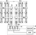
도 6은 도 1의 메모리 어레이를 설명하기 위한 블록도이다. 도 7은 도 1의 메모리 어레이를 설명하기 위한 회로도이다.6 is a block diagram illustrating the memory array of FIG. 7 is a circuit diagram for explaining the memory array of FIG.
도 6 및 도 7을 참조하면, 도 5에서 설명한 메모리 블록층들이 적어도 2층 이상 적층되며, 바람직한 실시예에서는 메모리 블록층들(110BL0~110BL3)이 4층으로 적층된다. 홀수 메모리 블록층(110BL0 또는 110BL2)에 포함된 메모리 블록들(또는 메모리 스트링들)과 짝수 메모리 블록층(110BL1 또는 110BL3)에 포함된 메모리 블록들(또는 메모리 스트링들)은 비트라인들(BLA0~BLAk 또는 BLB0~BLBk)을 공유하거나 공통 소스 라인들(SLB_0~SLB_m)을 공유할 수 있다. 즉, 최하부 메모리 블록층(110BL0)과 최하부 메모리 블록층(110BL0)의 상부에 위치하는 메모리 블록층(110BL1)이 제1 하부 비트라인들(BLA0~BLAk)을 공유하고, 최상부 메모리 블록층(110BL3)과 최상부 메모리 블록층(110BL3)의 하부에 위치하는 메모리 블록층(110BL2)이 제1 상부 비트라인들(BLB0~BLBk)을 공유할 수 있다.Referring to FIGS. 6 and 7, at least two or more memory block layers shown in FIG. 5 are stacked, and in a preferred embodiment, the memory block layers 110BL0 to 110BL3 are stacked in four layers. The memory blocks (or memory strings) included in the odd memory block layer 110BL0 or 110BL2 and the memory blocks (or memory strings) included in the even memory block layer 110BL1 or 110BL3 are connected to the bit lines BLA0- BLAk or BLB0 to BLBk, or may share common source lines SLB_0 to SLB_m. That is, the memory block layer 110BL1 located above the lowermost memory block layer 110BL0 and the lowest memory block layer 110BL0 share the first lower bit lines BLA0 to BLAk and the uppermost memory block layer 110BL3 And the memory block layer 110BL2 located under the uppermost memory block layer 110BL3 may share the first upper bit lines BLB0 to BLBk.
구체적으로 예를 들면, 홀수 메모리 블록층(예, 110BL2)은 상부에 적층된 짝수 메모리 블록층(110BL3)과 비트라인들(BLB0~BLBk)을 공유하고, 하부에 적층된 짝수 메모리 블록층(110BL1)과 공통 소스 라인들(SL)을 공유할 수 있다. 또한, 짝수 메모리 블록층(예, 110BL1)이 상부에 적층된 홀수 메모리 블록층(110BL2)과 공통 소스 라인들(SL)을 공유하고, 하부에 적층된 홀수 메모리 블록층(110BL0)과 비트 라인들(BLA0~BLAk)을 공유할 수도 있다. 이를 위해, 비트라인들(BLA0~BLAk)과 비트라인들(BLB0~BLBk)이 서로 다른층에 각각 형성되고, 공통 소스 라인들(SL)이 각각 서로 다른 층에 형성될 수 있다.More specifically, for example, the odd memory block layer (e.g., 110BL2) shares the bit line BLB0 to BLBk with the even memory block layer 110BL3 stacked on the top, and the even memory block layer 110BL1 ) And the common source lines (SL). The odd memory block layer 110BL1 shared with the even memory block layer 110BL1 and the common source lines SL shared with the odd memory block layer 110BL0 and the bit lines 110BL0, (BLA0 to BLAk). To this end, the bit lines BLA0 to BLAk and the bit lines BLB0 to BLBk may be formed in different layers, respectively, and the common source lines SL may be formed in different layers.
상기와 같이 메모리 블록층들(110BL0~110BL3)이 비트라인들(BLA0~BLAk, BLB0~BLBk) 및 공통 소스 라인들(SL)을 공유하기 위해서는, 홀수 메모리 블록층(110BL0, 110BL2)에 포함된 메모리 블록과 짝수 메모리 블록층(110BL1, 110BL3)에 포함된 메모리 블록이 수직으로 대칭이 되도록 메모리 블록층들이 적층되는 것이 바람직하다.In order for the memory block layers 110BL0 to 110BL3 to share the bit lines BLA0 to BLAk and BLB0 to BLBk and the common source lines SL as described above, It is preferable that the memory block layers are stacked such that the memory blocks included in the memory block and the even memory block layers 110BL1 and 110BL3 are vertically symmetrical.
특히, 하부 비트라인들(BLA0~BLAk)과 상부 비트라인들(BLB0~BLBk)은 수직 배선에 의해 서로 연결된다. 하부 비트라인들(BLA0~BLAk)과 상부 비트라인들(BLB0~BLBk)은 메모리 어레이의 외곽에서 연결되거나 메모리 어레이의 중앙에서 연결될 수 있다. 구체적은 연결 방식은 후술하기로 한다.In particular, the lower bit lines BLA0 to BLAk and the upper bit lines BLB0 to BLBk are connected to each other by vertical wiring. The lower bit lines BLA0 to BLAk and the upper bit lines BLB0 to BLBk may be connected at the periphery of the memory array or at the center of the memory array. Specifically, the connection method will be described later.
메모리 블록층들(110BL0~110BL3)은 워드라인들(WLA0~WLAn)을 서로 공유한다. 즉, 메모리 블록층들(110BL0~110BL4)의 워드라인들(WLA0~WLAn)이 수직으로 서로 연결된다. 좀 더 구체적으로, 메모리 블록층들(110BL0~110BL4)에 각각 포함된 첫 번째 메모리 블록들의 워드라인들(WLA0~WLAn)이 서로 수직으로 연결된다. 그리고, 메모리 블록층들(110BL0~110BL4)에 각각 포함된 마지막 번째 메모리 블록들의 워드라인들이 서로 수직으로 연결된다. 즉, 서로 다른 메모리 블록들의 워드라인들이 수직으로 연결되지만 수평으로 연결되지는 않는다.The memory block layers 110BL0 to 110BL3 share the word lines WLA0 to WLAn. That is, the word lines WLA0 to WLAn of the memory block layers 110BL0 to 110BL4 are vertically connected to each other. More specifically, the word lines WLA0 to WLAn of the first memory blocks included in the memory block layers 110BL0 to 110BL4 are vertically connected to each other. The word lines of the last memory blocks included in the memory block layers 110BL0 to 110BL4 are vertically connected to each other. That is, the word lines of different memory blocks are connected vertically but not horizontally.
메모리 블록층들(110BL0~110BL3)은 공통 소스 라인들(SL)을 서로 공유한다. 즉, 메모리 블록층들(110BL0~110BL4)의 공통 소스 라인들(SL)이 수직으로 서로 연결된다. 워드라인들(WLA0~WLAn)과 마찬가지로, 서로 다른 메모리 블록들의 공통 소스 라인들이 수직으로 연결되지만 수평으로 연결되지는 않는다.The memory block layers 110BL0 to 110BL3 share the common source lines SL with each other. That is, the common source lines SL of the memory block layers 110BL0 to 110BL4 are vertically connected to each other. As with the word lines WLA0 to WLAn, the common source lines of the different memory blocks are connected vertically but not horizontally.
메모리 블록층들(110BL0~110BL3)의 소스 선택 라인들(SGS0_0~SGS0_j, SGS1_0~SGS1_j, SGS2_0~SGS2_j, SGS3_0~SGS3_j)은 서로 분리된다. 보다 구체적으로, 수평이나 수직으로 인접한 다른 메모리 블록들의 소스 선택 라인들은 서로 연결되지는 않는다. 메모리 블록층들(110BL0~110BL3)의 드레인 선택 라인들(SGD0_0~SGD0_i, SGD1_0~SGD1_i, SGD2_0~SGD2_i, SGD3_0~SGD3_i)은 서로 분리된다. 보다 구체적으로, 수평이나 수직으로 인접한 다른 메모리 블록들의 드레인 선택 라인들은 서로 연결되지는 않는다. 이렇듯, 워드라인들, 비트라인들 및 공통 소스 라인들은 각각 수직으로 연결되지만, 선택 라인들은 수직으로 분리된다.The source selection lines SGS0_0 to SGS0_j, SGS1_0 to SGS1_j, SGS2_0 to SGS2_j, and SGS3_0 to SGS3_j of the memory block layers 110BL0 to 110BL3 are separated from each other. More specifically, the source select lines of the other memory blocks adjacent horizontally or vertically are not connected to each other. The drain select lines SGD0_0 to SGD0_i, SGD1_0 to SGD1_i, SGD2_0 to SGD2_i, and SGD3_0 to SGD3_i of the memory block layers 110BL0 to 110BL3 are separated from each other. More specifically, the drain select lines of the other memory blocks adjacent horizontally or vertically are not connected to each other. As such, the word lines, bit lines, and common source lines are each connected vertically, but the select lines are vertically separated.
다시 도 1을 참조하면, 전압 공급 회로(120)는 리드 동작, 프로그램 동작 또는 소거 동작과 같이 메모리 블록들 중 선택된 메모리 블록의 데이터 입출력 동작을 위하여 메모리 블록들로 동작 전압들을 인가하도록 구성된다. 기본적으로, 전압 공급 회로(120)는 리드 동작 시 선택된 메모리 셀들의 워드라인(선택된 워드라인)에 리드 전압을 인가하고 비선택 메모리 셀들의 워드라인들(비선택 워드라인들)에 리드 패스 전압을 인가할 수 있다. 또한, 전압 공급 회로(120)는 프로그램 동작 시 선택된 메모리 셀들의 워드라인(선택된 워드라인)에 프로그램 전압을 인가하고 비선택 메모리 셀들의 워드라인들(비선택 워드라인들)에 프로그램 패스 전압을 인가할 수 있다. 또한, 전압 공급 회로(120)는 소거 동작 시 메모리 셀들의 워드라인들(WL0~WLn)에 음전압(예, -10V)을 인가할 수 있다.Referring again to FIG. 1, the voltage supply circuit 120 is configured to apply operating voltages to memory blocks for data input / output operations of selected memory blocks among the memory blocks, such as a read operation, a program operation, or an erase operation. Basically, the voltage supply circuit 120 applies a read voltage to a word line (selected word line) of selected memory cells during a read operation and applies a read pass voltage to word lines (unselected word lines) of unselected memory cells . In addition, the voltage supply circuit 120 applies a program voltage to a word line (selected word line) of selected memory cells during a program operation and applies a program pass voltage to word lines (unselected word lines) of unselected memory cells can do. In addition, the voltage supply circuit 120 may apply a negative voltage (e.g., -10 V) to the word lines WL0 to WLn of the memory cells during the erase operation.
한편, 워드라인들(WL0~WLn), 공통 소스라인(SL) 및 비트라인들(BL0~BLk)을 통해 선택된 메모리 블록으로 인가되는 동작 전압들이 상부 또는 하부에 위치하는 비선택 메모리 블록들에도 인가된다. 따라서, 선택된 메모리 블록에서만 리드 동작, 프로그램 동작 또는 소거 동작이 실시되고 비선택 메모리 블록에서는 간섭 현상이나 디스터브 현상이 최소화될 수 있도록, 전압 공급 회로(120)는 각 층별로 드레인 선택 라인들(SGD0_0~SGD0_i, SGD1_0~SGD1_i, SGD2_0~SGD2_i, SGD3_0~SGD3_i)에 인가되는 동작 전압들을 독립적으로 제어하고, 소스 선택 라인들(SGS0_0~SGS_i, SGS1_0~SGS1_i, SGS2_0~SGS2_i, SGS3_0~SGS3_i)에 인가되는 동작 전압들을 독립적으로 제어하는 것이 바람직하다.On the other hand, operating voltages applied to the selected memory block through the word lines WL0 to WLn, the common source line SL and the bit lines BL0 to BLk are also applied to the unselected memory blocks located at the upper portion or the lower portion do. Therefore, in order to minimize the interference phenomenon and the disturb phenomenon in the unselected memory block, the voltage supply circuit 120 supplies the drain selection lines SGD0_0 to SGD0_0 to the respective layers in order to perform the read operation, the program operation or the erase operation only in the selected memory block, (SGS0_0 to SGS_i, SGS1_0 to SGS1_i, SGS2_0 to SGS2_i, SGS3_0 to SGS3_i) independently of the operation voltages applied to the source selection lines (SGD0_i, SGD1_0 to SGD1_i, SGD2_0 to SGD2_i, and SGD3_0 to SGD3_i) It is desirable to control the voltages independently.
이를 위해, 전압 공급 회로(120)는 드레인 선택 라인 드라이버들, 워드라인 드라이버들, 소스 선택 라인 드라이버들 및 공통 소스 라인 드라이버를 포함할 수 있다. 제1 드레인 선택 라인 드라이버, 제1 워드라인 드라이버 및 제1 소스 선택 라인 드라이버가 하나의 드라이버 그룹이 되고, 하나의 드라이버 그룹은 메모리 블록층들(110BL0~110BL3)에 각각 포함된 메모리 블록들이 공유하는 워드라인들(WL0~WLn) 및 선택 라인들(SGD0_0~SGD0_i, SGD1_0~SGD1_i, SGD2_0~SGD2_i, SGD3_0~SGD3_i, SGS0_0~SGS_i, SGS1_0~SGS1_i, SGS2_0~SGS2_i, SGS3_0~SGS3_i)에 인가되는 동작 전압들을 각각 제어한다. 즉, 드라이버 그룹은 각각의 메모리 블록층에 포함된 메모리 블록들의 수만큼 구비될 수 있다.To this end, the voltage supply circuit 120 may include drain select line drivers, word line drivers, source select line drivers, and a common source line driver. The first drain select line driver, the first word line driver, and the first source select line driver become one driver group, and one driver group is formed by the memory block layers 110BL0 through 110BL3, The operation voltage applied to the word lines WL0 to WLn and the selection lines SGD0_0 to SGD0_i, SGD1_0 to SGD1_i, SGD2_0 to SGD2_i, SGD3_0 to SGD3_i, SGS0_0 to SGS_i, SGS1_0 to SGS1_i, SGS2_0 to SGS2_i, SGS3_0 to SGS3_i, Respectively. That is, the driver group may be provided for the number of memory blocks included in each memory block layer.
읽기/쓰기 회로(130)는 비트라인들(BL0~BLk)을 통해 메모리 블록층들(110BL0~110B4)에 포함된 메모리 블록들과 연결된다. 또한, 읽기/쓰기 회로(150)는 프로그램 동작 시 메모리 셀들에 저장되는 데이터에 따라 선택된 비트라인들(BL0~BLk)을 선택적으로 프리차지하거나 디스차지하고, 리드 동작 시 선택된 비트라인들(BL0~BLk)의 전압 변화(또는 전류 변화)를 센싱하여 메모리 셀들에 저장된 데이터를 래치한다. 이러한 읽기/쓰기 회로(130)는 페이지 버퍼를 포함할 수 있다.
The read /
이하, 상부 비트라인들과 하부 비트라인들의 연결 방식과 메모리 블록들로 인가되는 동작 전압들의 구체적인 실시예들을 설명하기로 한다.Hereinafter, a detailed description will be given of a connection method of the upper bit lines and the lower bit lines and specific embodiments of the operating voltages applied to the memory blocks.
도 8 내지 도 10, 도 11a 및 도 11b는 본 발명의 실시예들에 따른 반도체 메모리 장치의 연결 구조 및 동작을 설명하기 위한 도면들이다.FIGS. 8 to 10, FIGS. 11A and 11B are views for explaining the connection structure and operation of the semiconductor memory device according to the embodiments of the present invention.
도 8을 참조하면, 제1 및 제2 메모리 블록층들(110BL0, 110BL1)이 공유하는 하부 비트라인(BLA)과 제3 및 제4 메모리 블록층들(110BL2, 110BL3)이 공유하는 상부 비트라인(BLB)이 수직 배선(VL)에 의해 연결될 수 있다. 여기서, 수직 배선(VL)은 콘택 플러그(CT)와 콘택 패드(PAD)를 포함할 수 있다. 콘택 플러그(CT)는 메모리 스트링(ST)과 동일층에 형성되고, 콘택 패드(PAD)는 공통 소스 라인(SL)과 동일층에 형성될 수 있다. 콘택 플러그(CT)와 콘택 패드(PAD)의 일부는 상부 비트라인(BLB)과 하부 비트라인(BLA) 사이에 형성되어 상부 비트라인(BLB)과 하부 비트라인(BLA)을 연결한다. 콘택 플러그(CT)와 콘택 패드(PAD)의 나머지는 하부 비트라인(BLA)과 기판 사이에 형성되고, 하부 비트라인(BLA)과 읽기/쓰기 회로(130)를 전기적으로 연결하기 위한 역할을 할 수 있다. 수직 배선(VL)에 의해 상부 비트라인(BLB)과 하부 비트라인(BLA)이 모두 동일한 읽기/쓰기 회로(130)에 연결된다.Referring to FIG. 8, the lower bit line BLA shared by the first and second memory block layers 110BL0 and 110BL1 and the upper bit line BLA shared by the third and fourth memory block layers 110BL2 and 110BL3, (BLB) can be connected by the vertical wiring VL. Here, the vertical wiring VL may include a contact plug CT and a contact pad PAD. The contact plug CT may be formed on the same layer as the memory string ST and the contact pad PAD may be formed on the same layer as the common source line SL. A part of the contact plug CT and the contact pad PAD is formed between the upper bit line BLB and the lower bit line BLA to connect the upper bit line BLB and the lower bit line BLA. The remainder of the contact plug CT and the contact pad PAD is formed between the lower bit line BLA and the substrate and functions to electrically connect the lower bit line BLA and the read / . The upper bit line BLB and the lower bit line BLA are both connected to the same read /
수직 배선(VL)은 메모리 어레이(MA)의 가장자리에 정의된 콘택 영역(CA)에 형성될 수 있다. 특히, 상부 비트라인(BLB)과 하부 비트라인(BLA)을 연결하기 위한 배선과 하부 비트라인(BLA)을 기판과 연결하기 위한 배선이 수직으로 동일한 영역에 형성되므로, 수직 배선(VL)이 형성되는 콘택 영역(CA)을 줄일 수 있다. 그 결과, 칩 사이즈를 줄일 수 있다.The vertical wiring VL may be formed in the contact area CA defined at the edge of the memory array MA. In particular, since the wiring for connecting the upper bit line BLB and the lower bit line BLA and the wiring for connecting the lower bit line BLA to the substrate are formed in the same vertical region, the vertical wiring VL is formed The contact area CA can be reduced. As a result, the chip size can be reduced.
한편, 읽기/쓰기 회로(130)는 비트라인 스위칭 회로(131), 래치 회로(132) 및 BL 전압 공급 회로(133)를 포함한다. 비트라인 스위칭 회로(131)는 비트라인 선택 신호(SEL)에 응답하여 동작하는 트랜지스터(N1)와 비트라인 선택 반전 신호(/SEL)에 응답하여 동작하는 트랜지스터(N2)를 포함한다. 비트라인 스위칭 회로(131)는 신호들(SEL, /SEL)에 응답하여 비트라인(BL)이 선택되면 비트라인(BL)을 래치 회로(132)와 연결시키고, 비트라인(BL)이 비선택되면 비트라인(BL)을 BL 전압 공급 회로(133)와 연결시킨다. 비트라인(BL)이 래치회로(132)에 연결되면 정상적으로 프로그램 동작이나 리드 동작이 진행되고, 비트라인(BL)이 BL 전압 공급 회로(133)에 연결되면, BL 전압 공급 회로(133)에 의해 프로그램 동작 시 비트라인(BL)에는 프로그램 금지 전압(예, 전원 전압)이 인가되고 리드 동작 시 접지 전압(예, 0V) 또는 프리자치 전압이 인가될 수 있다.On the other hand, the read /
상기의 구조로 비트라인들(BLA, BLB)이 연결된 경우 전압 공급 회로(도 1의 120)와 읽기/쓰기 회로(130)는 리드 동작, 프로그램 동작 및 소거 동작 시 다음 표 1에서와 같이 동작 전압들을 인가할 수 있다.
When the bit lines BLA and BLB are connected in the above structure, the voltage supply circuit 120 (FIG. 1) and the read /
[표 1][Table 1]

도 7과 표 1을 참조하면, 선택된 메모리 스트링(ST2_0)과 비선택 메모리 스트링들(ST0, ST1, ST3)은 워드라인들(WL0~WLn), 비트라인들(BL0~BLk) 및 공통 소스 라인(SL)을 공유하기 때문에, 메모리 스트링들(ST0, ST1, ST2_0, ST3)로 동일한 동작 전압들(예, 리드 전압, 프로그램 전압, 패스 전압 등등)이 인가된다. 비선택 메모리 스트링들(ST0, ST1, ST3)의 리드 동작, 프로그램 동작 또는 소거 동작을 차단하기 위하여 선택 라인들에 서로 다른 동작 전압들이 인가된다.7 and Table 1, the selected memory string ST2_0 and the unselected memory strings ST0, ST1 and ST3 are connected to the word lines WL0 to WLn, the bit lines BL0 to BLk, The same operating voltages (e.g., read voltage, program voltage, pass voltage, etc.) are applied to the memory strings ST0, ST1, ST2_0, and ST3. Different operating voltages are applied to the select lines to block the read operation, the program operation, or the erase operation of the unselected memory strings ST0, ST1, and ST3.
예를 들어, 비선택 메모리 스트링들(ST0, ST1, ST3)의 리드 동작을 차단하기 위하여, 비선택 메모리 스트링들(ST0, ST1, ST3)의 소스 선택 라인(SGS0_0, SGS1_0, SGS3_0)에 접지 전압을 인가한다. 접지 전압에 의해 비선택 메모리 스트링들(ST0, ST1, ST3)의 소스 선택 트랜지스터가 턴오프되고 비선택 메모리 스트링들(ST0, ST1, ST3)은 공통 소스 라인(SL)과 분리된다. 그 결과, 비선택 메모리 스트링들(ST0, ST1, ST3)은 선택된 메모리 스트링(ST2_0)의 리드 동작에 영향을 주지 않는다.The source selection lines SGS0_0, SGS1_0 and SGS3_0 of the unselected memory strings ST0, ST1 and ST3 are connected to the ground voltage VSS to prevent the read operation of the unselected memory strings ST0, ST1 and ST3, for example. . The source selection transistors of the unselected memory strings ST0, ST1 and ST3 are turned off by the ground voltage and the unselected memory strings ST0, ST1 and ST3 are separated from the common source line SL. As a result, the unselected memory strings ST0, ST1, and ST3 do not affect the read operation of the selected memory string ST2_0.
비선택 메모리 스트링들(ST0, ST1, ST3)의 프로그램 동작을 차단하기 위하여, 비선택 메모리 스트링들(ST0, ST1, ST3)의 드레인 선택 라인(SGD0_0, SGD1_0, SGD3_0)에 채널의 프리차지를 위한 양전압(예, 5V)을 인가한 후 접지 전압(예, 0V) 또는 음전압(예, -2V)을 인가한다. 패스 전압(Vpass_pgm)이 인가되면 드레인 선택 트랜지스터가 턴오프되고 비선택 메모리 스트링들(ST0, ST1, ST3)은 비트 라인(BL0)과 분리된다. 그 결과, 비선택 메모리 스트링들(ST0, ST1, ST3)에 포함된 메모리 셀들의 프로그램이 금지된다.To block the program operation of the unselected memory strings ST0, ST1 and ST3, the drain select lines SGD0_0, SGD1_0 and SGD3_0 of the unselected memory strings ST0, ST1 and ST3 are precharged After applying a positive voltage (for example, 5V), apply a ground voltage (for example, 0V) or a negative voltage (for example, -2V). When the pass voltage Vpass_pgm is applied, the drain select transistor is turned off and the unselected memory strings ST0, ST1, and ST3 are separated from the bit line BL0. As a result, programming of the memory cells included in the unselected memory strings ST0, ST1, and ST3 is prohibited.
비선택 메모리 스트링들(ST0, ST1, ST3)의 소거 동작을 차단하기 위하여, 비선택 메모리 스트링들(ST0, ST1, ST3)의 소스 선택 라인(SGS0_0, SGS1_0, SGS3_0)에 접지 전압(예, 0V) 또는 음전압(예, -2V)을 인가한다. 그 결과, 비선택 메모리 스트링들(ST0, ST1, ST3)의 채널 전압이 부스팅 현상에 의해 높아지고, 비선택 메모리 스트링들(ST0, ST1, ST3)에 포함된 메모리 셀들의 소거가 금지된다.The source selection lines SGS0_0, SGS1_0 and SGS3_0 of the unselected memory strings ST0, ST1 and ST3 are grounded (for example, 0V) to the erasing operation of the unselected memory strings ST0, ST1 and ST3 ) Or a negative voltage (for example, -2 V). As a result, the channel voltage of the unselected memory strings ST0, ST1, and ST3 is increased by the boosting phenomenon, and the erasing of the memory cells included in the unselected memory strings ST0, ST1, and ST3 is inhibited.
도 9를 참조하면, 제1 및 제2 메모리 블록층들(110BL0, 110BL1)이 공유하는 하부 비트라인(BLA)과 제3 및 제4 메모리 블록층들(110BL2, 110BL3)이 공유하는 상부 비트라인(BLB)을 연결하는 수직 배선(VL)이 메모리 어레이의 중앙에 위치할 수 있다. 즉, 메모리 블록층들(110BL0, 110BL1, 110BL2, 110BL3)의 메모리 블록들을 2개의 메모리 블록 그룹들(MA_L, MA_R)로 각각 나누고, 메모리 블록 그룹들(MA_L, MA_R) 사이에 비트라인들(BLA, BLB)을 수직으로 연결하기 위한 수직 배선(VL)을 형성할 수 있다.Referring to FIG. 9, the lower bit line BLA shared by the first and second memory block layers 110BL0 and 110BL1 and the upper bit line BLA shared by the third and fourth memory block layers 110BL2 and 110BL3 (VL) connecting the bit lines BLB may be located at the center of the memory array. That is, the memory blocks of the memory block layers 110BL0, 110BL1, 110BL2 and 110BL3 are divided into two memory block groups MA_L and MA_R and the bit lines BLA , BLB can be formed vertically.
상기의 구조로 비트라인들(BLA, BLB)이 연결된 경우 전압 공급 회로(도 1의 120)와 읽기/쓰기 회로(130)는 리드 동작, 프로그램 동작 및 소거 동작 시 다음 표 2에서와 같이 동작 전압들을 인가할 수 있다. 비선택 메모리 스트링들(ST0, ST1, ST3)의 리드 동작, 프로그램 동작 또는 소거 동작을 차단하기 위하여 선택 라인들에 서로 다른 동작 전압들이 표 1에 설명한 바와 같이 인가될 수 있다.When the bit lines BLA and BLB are connected in the above structure, the voltage supply circuit 120 (FIG. 1) and the read /
[표 2][Table 2]

도 10을 참조하면, 메모리 블록층들(110BL0, 110BL1, 110BL2, 110BL3)의 메모리 블록들을 2개의 메모리 블록 그룹들(MA_L, MA_R)로 각각 나누고, 제1 메모리 블록 그룹(MA_L)의 비트라인들(BLA_L, BLB_L)을 제2 메모리 블록 그룹(MA_R)의 비트라인들(BLA_R, BLB_R)과 분리할 수 있다. 그리고, 메모리 블록 그룹들(MA_L, MA_R) 사이에, 제1 메모리 블록 그룹(MA_L)의 하부 비트라인(BLA_L) 및 상부 비트라인(BLB_L)을 연결하기 위한 제1 수직 배선(VL1)과 제2 메모리 블록 그룹(MA_R)의 하부 비트라인(BLA_R) 및 상부 비트라인(BLB_R)을 연결하기 위한 제2 수직 배선(VL2)이 형성될 수 있다.10, the memory blocks of the memory block layers 110BL0, 110BL1, 110BL2 and 110BL3 are divided into two memory block groups MA_L and MA_R, and the bit lines of the first memory block group MA_L (BLA_L, BLB_L) from the bit lines (BLA_R, BLB_R) of the second memory block group (MA_R). A first vertical wiring line VL1 for connecting the lower bit line BLA_L and the upper bit line BLB_L of the first memory block group MA_L and a second vertical wiring line VL2 for connecting the lower bit line BLA_L and the upper bit line BLB_L are provided between the memory block groups MA_L and MA_R. A second vertical wiring VL2 for connecting the lower bit line BLA_R and the upper bit line BLB_R of the memory block group MA_R may be formed.
제1 메모리 블록 그룹(MA_L)에서 선택된 메모리 스트링(ST2_0)의 리드 동작, 프로그램 동작 및 소거 동작 시, 전압 공급 회로(도 1의 120)와 읽기/쓰기 회로(130)는 다음 표 3에서와 같이 동작 전압들을 인가할 수 있다. 동일한 동작 전압들이 인가되는 비선택 메모리 스트링들(ST0, ST1, ST3)의 리드 동작, 프로그램 동작 또는 소거 동작을 차단하기 위하여, 선택 라인들에 서로 다른 동작 전압들이 표 1에 설명한 바와 같이 인가될 수 있다.In the read operation, program operation and erase operation of the selected memory string ST2_0 in the first memory block group MA_L, the voltage supply circuit 120 (FIG. 1) and the read /
[표 3][Table 3]

읽기/쓰기 회로(130)의 비트라인 스위칭 회로(131)는 제1 메모리 블록 그룹(MA_L)을 선택하는 제1 선택 신호(SEL1), 제2 메모리 블록 그룹(MA_R)을 선택하는 제2 선택 신호(SEL2) 및 이들의 반전 신호들(/SEL1, /SEL2)에 응답하여, 선택된 메모리 블록 그룹의 비트라인(예, BL_L)을 래치 회로(132)에 연결하고 비선택된 메모리 블록 그룹의 비트라인(예, BL_R)을 BL 전압 공급 회로(133)로 연결할 수 있다.The bit
상기의 실시예는 비트라인들의 길이가 반으로 줄어들기 때문에 비트라인들을 프리차지하는 시간을 줄일 수 있으며 비트라인들 간의 간섭 현상에 의한 특정 저하를 감소시킬 수 있다.Since the length of the bit lines is reduced by half, the time for precharging the bit lines can be shortened and the specific degradation due to the interference phenomenon between the bit lines can be reduced.
도 11a 및 도 11b를 참조하면, 메모리 블록층들(110BL0, 110BL1, 110BL2, 110BL3)의 메모리 블록들을 2개의 메모리 블록 그룹들(MA_L, MA_R)로 각각 나누고, 제1 메모리 블록 그룹(MA_L)의 비트라인들(BLA_B, BLB_A)을 제2 메모리 블록 그룹(MA_R)의 비트라인들(BLA_A, BLB_B)과 분리할 수 있다. 그리고, 메모리 블록 그룹들(MA_L, MA_R) 사이에, 제1 메모리 블록 그룹(MA_L)의 하부 비트라인(BLA_B) 및 제2 메모리 블록 그룹(MA_R)의 상부 비트라인(BLB_B)을 연결하고, 제1 메모리 블록 그룹(MA_L)의 상부 비트라인(BLA_A) 및 제2 메모리 블록 그룹(MA_R)의 하부 비트라인(BLA_A)을 연결하기 위한 수직 배선(VL)이 형성될 수 있다.11A and 11B, the memory blocks of the memory block layers 110BL0, 110BL1, 110BL2 and 110BL3 are divided into two memory block groups MA_L and MA_R, and the memory blocks of the first memory block group MA_L The bit lines BLA_B and BLB_A can be separated from the bit lines BLA_A and BLB_B of the second memory block group MA_R. The lower bit line BLA_B of the first memory block group MA_L and the upper bit line BLB_B of the second memory block group MA_R are connected between the memory block groups MA_L and MA_R, A vertical wiring VL for connecting the upper bit line BLA_A of one memory block group MA_L and the lower bit line BLA_A of the second memory block group MA_R may be formed.
제1 메모리 블록 그룹(MA_L)에서 선택된 메모리 스트링(ST2_0)의 리드 동작, 프로그램 동작 및 소거 동작 시, 전압 공급 회로(도 1의 120)와 읽기/쓰기 회로(130)는 다음 표 4에서와 같이 동작 전압들을 인가할 수 있다.In the read operation, the program operation and the erase operation of the selected memory string ST2_0 in the first memory block group MA_L, the voltage supply circuit 120 (FIG. 1) and the read /
[표 4][Table 4]

워드라인들(WL0~WLn)로 동일한 동작 전압들이 인가되는 비선택 메모리 스트링들(ST0, ST1, ST3)의 리드 동작, 프로그램 동작 또는 소거 동작을 차단하기 위하여, 선택 라인들에 서로 다른 동작 전압들이 표 1에 설명한 바와 같이 인가될 수 있다. 또한, 워드라인들(WL0~WLn)로 동일한 동작 전압들이 인가되는 스트링들 중 하부 메모리 스트링들(ST0, ST1)이 공유하는 비트라인(BLA_B)과 상부 메모리 스트링들(ST2_0, ST3)이 공유하는 비트라인(BLB_A)이 분리된다. 따라서, 선택된 메모리 스트링(ST2_0)의 리드 동작이나 프로그램 동작 시 비선택 하부 메모리 스트링들(ST0, ST1)이 공유하는 하부 비트라인(BLA_B)에 프리차지 전압(예, Vcc)이나 프로글매 금지 전압(예, Vcc)을 인가함으로써, 비선택 하부 메모리 스트링들(ST0, ST1)에 포함된 메모리 셀들의 리드 디스터브(read disturb) 특성과 프로그램 디스터브(program disturb) 특성을 개선할 수 있다.
In order to block the read operation, the program operation or the erase operation of the unselected memory strings ST0, ST1 and ST3 to which the same operation voltages are applied to the word lines WL0 to WLn, Lt; RTI ID = 0.0 > 1 < / RTI > The bit lines BLA_B and the upper memory strings ST2_0 and ST3 shared by the lower memory strings ST0 and ST1 among the strings to which the same operating voltages are applied to the word lines WL0 to WLn are shared The bit line BLB_A is disconnected. Therefore, a precharge voltage (e.g., Vcc) or a programming inhibition voltage (e.g., Vcc) is applied to the lower bit line BLA_B shared by the unselected lower memory strings ST0 and ST1 during a read operation or a program operation of the selected memory string ST2_0 The read disturb characteristic and the program disturb characteristic of the memory cells included in the unselected lower memory strings ST0 and ST1 can be improved by applying the threshold voltage Vcc (for example, Vcc).
도 12는 본 발명의 실시예에 따른 메모리 시스템을 간략히 보여주는 블록도이다.12 is a block diagram briefly showing a memory system according to an embodiment of the present invention.
도 12를 참조하면, 본 발명의 실시예에 따른 메모리 시스템(1200)은 불휘발성 메모리 장치(1220)와 메모리 컨트롤러(1210)를 포함한다.Referring to FIG. 12, a
불휘발성 메모리 장치(1220)는 앞서 설명한 반도체 메모리 장치로 구성될 수 있다. 메모리 컨트롤러(1210)는 프로그램 루프, 리드 동작이나 소거 루프와 같은 일반 동작 모드에서 불휘발성 메모리 장치(1220)를 제어하도록 구성된다.The
불휘발성 메모리 장치(1220)와 메모리 컨트롤러(1210)의 결합에 의해 메모리 카드 또는 반도체 디스크 장치(Solid State Disk: SSD)로 제공될 수 있을 것이다. SRAM(1211)은 프로세싱 유닛(1212)의 동작 메모리로써 사용된다. 호스트 인터페이스(1213)는 메모리 시스템(1200)과 접속되는 호스트의 데이터 교환 프로토콜을 구비한다. 에러 정정 블록(1214)은 불휘발성 메모리 장치(1220)로부터 독출된 데이터에 포함되는 에러를 검출 및 정정한다. 메모리 인터페이스(1214)는 본 발명의 불휘발성 메모리 장치(1220)와 인터페이싱 한다. 프로세싱 유닛(1212)은 메모리 컨트롤러(1210)의 데이터 교환을 위한 제반 제어 동작을 수행한다.May be provided as a memory card or a solid state disk (SSD) by the combination of the
비록 도면에는 도시되지 않았지만, 본 발명에 따른 메모리 시스템(1200)은 호스트(Host)와의 인터페이싱을 위한 코드 데이터를 저장하는 ROM(미도시됨) 등이 더 제공될 수 있음은 이 분야의 통상적인 지식을 습득한 자들에게 자명하다. 불휘발성 메모리 장치(1220)는 복수의 플래시 메모리 칩들로 구성되는 멀티-칩 패키지로 제공될 수도 있다. 이상의 본 발명의 메모리 시스템(1200)은 에러의 발생 확률이 낮은 고신뢰성의 저장 매체로 제공될 수 있다. 특히, 최근 활발히 연구되고 있는 반도체 디스크 장치(Solid State Disk: 이하 SSD)와 같은 메모리 시스템에서 본 발명의 플래시 메모리 장치가 구비될 수 있다. 이 경우, 메모리 컨트롤러(1210)는 USB, MMC, PCI-E, SATA, PATA, SCSI, ESDI, 그리고 IDE 등과 같은 다양한 인터페이스 프로토콜들 중 하나를 통해 외부(예를 들면, 호스트)와 통신하도록 구성될 것이다.Although it is not shown in the drawing, the
도 13은 앞서 설명된 다양한 실시예들에 따라 프로그램 동작을 수행하는 퓨전 메모리 장치 또는 퓨전 메모리 시스템을 간략히 보여주는 블록도이다. 예를 들면, 퓨전 메모리 장치로서 원낸드 플래시 메모리 장치(1300)에 앞서 설명한 본 발명의 기술적 특징이 적용될 수 있다.13 is a simplified block diagram illustrating a fusion memory device or a fusion memory system that performs program operation in accordance with various embodiments described above. For example, the technical features of the present invention described above can be applied to the one-nAND
원낸드 플래시 메모리 장치(1300)는 서로 다른 프로토콜을 사용하는 장치와의 각종 정보 교환을 위한 호스트 인터페이스(1310)와, 메모리 장치를 구동하기 위한 코드를 내장하거나 데이터를 일시적으로 저장하는 버퍼 램(1320)과, 외부에서 주어지는 제어 신호와 명령어에 응답하여 읽기와 프로그램 및 모든 상태를 제어하는 제어부(1330)와, 명령어와 어드레스, 메모리 장치 내부의 시스템 동작 환경을 정의하는 설정(Configuration) 등의 데이터가 저장되는 레지스터(1340) 및 불휘발성 메모리 셀과 페이지 버퍼를 포함하는 동작 회로로 구성된 낸드 플래시 셀 어레이(1350)를 포함한다. 낸드 플래시 셀 어레이(1350)의 메모리 어레이는 도 2에 도시된 메모리 어레이가 적용될 수 있다.The OneNAND
도 14에는 본 발명에 따른 플래시 메모리 장치(1412)를 포함한 컴퓨팅 시스템이 개략적으로 도시되어 있다.14, a computing system including a
본 발명에 따른 컴퓨팅 시스템(1400)은 시스템 버스(1460)에 전기적으로 연결된 마이크로프로세서(1420), 램(1430), 사용자 인터페이스(1440), 베이스밴드 칩셋(Baseband chipset)과 같은 모뎀(1450) 및 메모리 시스템(1410)을 포함한다. 본 발명에 따른 컴퓨팅 시스템(1400)이 모바일 장치인 경우, 컴퓨팅 시스템(1400)의 동작 전압을 공급하기 위한 배터리(미도시됨)가 추가적으로 제공될 것이다. 비록 도면에는 도시되지 않았지만, 본 발명에 따른 컴퓨팅 시스템(1400)에는 응용 칩셋(Application chipset), 카메라 이미지 프로세서(Camera Image Processor: CIS), 모바일 디램, 등이 더 제공될 수 있음은 이 분야의 통상적인 지식을 습득한 자들에게 자명하다. 메모리 시스템(1410)은, 예를 들면, 데이터를 저장하는 데 불휘발성 메모리를 사용하는 SSD(Solid State Drive/Disk)를 구성할 수 있다. 또는, 메모리 시스템(1410)은, 퓨전 플래시 메모리(예를 들면, 원낸드 플래시 메모리)로 제공될 수 있다.
A
110 : 메모리 어레이110BL0~110BL3 : 메모리 블록층
MB : 메모리 블록120 : 전압 공급 회로
130 : 읽기/쓰기 회로131 : 비트라인 스위칭 회로
132 : 래치 회로133 : BL 전압 공급 회로110: memory array 110BL0 to 110BL3: memory block layer
MB: memory block 120: voltage supply circuit
130: read / write circuit 131: bit line switching circuit
132: latch circuit 133: BL voltage supply circuit
Claims (22)
Translated fromKorean상기 메모리 블록들과 연결되고 서로 다른 층들에 배열된 비트라인들을 연결하기 위한 제1 수직 배선들; 및
수직으로 배열된 상기 메모리 블록들의 워드라인들을 연결하기 위한 제2 수직 배선들을 포함하며,
수직으로 배열된 상기 메모리 블록들의 선택 라인들은 서로 분리되는 반도체 메모리 장치.
A memory array comprising memory blocks stacked in layers on a substrate;
First vertical interconnections connected to the memory blocks and for connecting bit lines arranged in different layers; And
Second vertical interconnections for connecting the word lines of the vertically arranged memory blocks,
And the selection lines of the memory blocks arranged vertically are separated from each other.
동일한 층에 배열된 상기 메모리 블록들의 워드라인들은 분리되는 반도체 메모리 장치.
The method according to claim 1,
And the word lines of the memory blocks arranged in the same layer are separated.
홀수 층에 배열된 상기 메모리 블록은 상부 짝수 층에 배열된 상기 메모리 블록과 상기 비트라인들을 공유하고, 하부 짝수 층에 배열된 상기 메모리 블록과 공통 소스 라인을 공유하는 반도체 메모리 장치.
The method according to claim 1,
Wherein the memory blocks arranged in the odd-numbered layers share the bit lines with the memory blocks arranged in the upper even-numbered layers, and share common source lines with the memory blocks arranged in the lower even-numbered layers.
상기 비트라인들과 상기 공통 소스 라인들은 서로 교차하는 방향으로 배열되는 반도체 메모리 장치.
The method of claim 3,
Wherein the bit lines and the common source lines are arranged in a direction crossing each other.
상기 짝수 층에 배열된 상기 메모리 블록과 상기 홀수 층에 배열된 상기 메모리 블록이 수직 대칭 구조로 적층되는 반도체 메모리 장치.
The method of claim 3,
Wherein the memory blocks arranged in the even-numbered layers and the memory blocks arranged in the odd-numbered layers are stacked in a vertically symmetric structure.
서로 다른 층에 배열된 상기 메모리 블록들의 상기 공통 소스 라인들이 서로 연결되고, 동일한 층에 배열된 상기 메모리 블록들의 상기 공통 소스 라인들이 서로 분리되는 반도체 메모리 장치.
The method of claim 3,
The common source lines of the memory blocks arranged in different layers are connected to each other and the common source lines of the memory blocks arranged in the same layer are separated from each other.
각각의 상기 메모리 블록은 상기 비트라인들과 공통 소스 라인 사이에 연결되는 메모리 스트링들을 포함하고,
각각의 상기 메모리 스트링에 포함된 메모리 셀들은 제1 선택 라인으로 인가되는 제1 선택 신호에 따라 공통 소스 라인과 전기적으로 연결되고 제2 선택 라인으로 인가되는 제2 선택 신호에 따라 상기 비트라인과 전기적으로 연결되는 반도체 메모리 장치.
The method according to claim 1,
Each said memory block including memory strings coupled between said bit lines and a common source line,
The memory cells included in each of the memory strings are electrically coupled to the common source line in accordance with a first select signal applied to the first select line and electrically connected to the bit line in accordance with a second select signal applied to the second select line. To the semiconductor memory device.
상기 공통 소스 라인과 연결되고 상기 제1 선택 신호에 따라 동작하는 제1 선택 트랜지스터와,
상기 비트라인과 연결되고 상기 제2 선택 신호에 따라 동작하는 제2 선택 트랜지스터와,
상기 제1 및 제2 선택 트랜지스터들 사이에 수직으로 직렬 연결되는 상기 메모리 셀들을 포함하는 반도체 메모리 장치.
8. The method of claim 7, wherein each said memory string comprises:
A first selection transistor connected to the common source line and operating in accordance with the first selection signal;
A second selection transistor connected to the bit line and operating in accordance with the second selection signal;
And the memory cells connected in series between the first and second selection transistors in series.
각각의 상기 메모리 블록 내에서 같은 비트라인에 연결되는 상기 메모리 스트링들의 상기 제1 선택 라인들이 서로 분리되고,
각각의 상기 메모리 블록 내에서 같은 비트라인에 연결되는 상기 메모리 스트링들의 상기 제2 선택 라인들이 서로 분리되는 반도체 메모리 장치.
8. The method of claim 7,
The first selection lines of the memory strings connected to the same bit line in each of the memory blocks are separated from each other,
The second select lines of the memory strings connected to the same bit line in each of the memory blocks are separated from each other.
서로 다른 층들에 수직으로 배열된 상기 메모리 블록들의 상기 제1 선택 라인들이 서로 분리되고,
서로 다른 층들에 수직으로 배열된 상기 메모리 블록들의 상기 제2 선택 라인들이 서로 분리되는 반도체 메모리 장치.
8. The method of claim 7,
The first selection lines of the memory blocks vertically arranged in different layers are separated from each other,
And the second selection lines of the memory blocks arranged vertically in different layers are separated from each other.
상기 제1 수직 배선들이 상기 메모리 어레이의 중앙에 위치하는 반도체 메모라 장치.
The method according to claim 1,
And the first vertical interconnections are located at the center of the memory array.
상기 비트라인들에 각각 연결되는 읽기/쓰기 회로들을 더 포함하는 반도체 메모리 장치.
The method according to claim 1,
Further comprising read / write circuits coupled to the bit lines, respectively.
상기 제1 메모리 어레이의 메모리 블록들 중 상부에 적층된 상기 메모리 블록들과 연결되는 제1 상부 비트라인들;
상기 제1 메모리 어레이의 메모리 블록들 중 하부에 적층된 상기 메모리 블록들과 연결되는 제1 하부 비트라인들;
상기 제2 메모리 어레이의 메모리 블록들 중 상부에 적층된 상기 메모리 블록들과 연결되는 제2 상부 비트라인들; 및
상기 제2 메모리 어레이의 메모리 블록들 중 하부에 적층된 상기 메모리 블록들과 연결되는 제2 하부 비트라인들을 포함하는 반도체 메모리 장치.
First and second memory arrays each comprising memory blocks stacked on a substrate;
First upper bit lines connected to the memory blocks stacked on top of the memory blocks of the first memory array;
First lower bit lines connected to the memory blocks stacked below the memory blocks of the first memory array;
Second upper bit lines connected to the memory blocks stacked on top of the memory blocks of the second memory array; And
And second lower bit lines connected to the memory blocks stacked below the memory blocks of the second memory array.
수직으로 배열된 상기 메모리 블록들의 워드라인들을 연결하기 위한 제3 배선들을 더 포함하는 반도체 메모리 장치.
14. The method of claim 13,
And third wires for connecting the word lines of the memory blocks arranged vertically.
상기 제1 및 제2 메모리 어레이들의 짝수 층에 배열된 상기 메모리 블록과 상기 홀수 층에 배열된 상기 메모리 블록이 수직 대칭 구조로 적층되는 반도체 메모리 장치.
14. The method of claim 13,
Wherein the memory blocks arranged in even layers of the first and second memory arrays and the memory blocks arranged in the odd numbered layers are stacked in a vertically symmetric structure.
상기 제1 메모리 어레이의 최하부 메모리 블록과 상기 최하부 메모리 블록의 상부에 위치하는 메모리 블록이 상기 제1 하부 비트라인들을 공유하고, 최상부 메모리 블록과 상기 최상부 메모리 블록의 하부에 위치하는 메모리 블록이 상기 제1 상부 비트라인들을 공유하고,
상기 제2 메모리 어레이의 최하부 메모리 블록과 상기 최하부 메모리 블록의 상부에 위치하는 메모리 블록이 상기 제2 하부 비트라인들을 공유하고, 최상부 메모리 블록과 상기 최상부 메모리 블록의 하부에 위치하는 메모리 블록이 상기 제2 상부 비트라인들을 공유하는 반도체 메모리 장치.
14. The method of claim 13,
Wherein a memory block located at a lower portion of the first memory array and a memory block located at an upper portion of the lowest memory block share the first lower bit lines and a memory block located below the uppermost memory block, 1 upper bit lines,
A memory block located at a lower portion of the second memory array and a memory block located at an upper portion of the lowest memory block share the second lower bit lines and a memory block located under the uppermost memory block, Lt; RTI ID = 0.0 > 2 < / RTI >
상기 제1 메모리 어레이의 메모리 블록들과 상기 제2 메모리 어레이의 메모리 블록들이 공통 소스 라인을 공유하는 반도체 메모리 장치.
14. The method of claim 13,
Wherein the memory blocks of the first memory array and the memory blocks of the second memory array share a common source line.
상기 제1 상부 비트라인들과 상기 제1 하부 비트라인들과 연결하기 위한 제1 배선들; 및
상기 제2 상부 비트라인들을 상기 제2 하부 비트라인들과 연결하기 위한 제2 배선들을 더 포함하는 반도체 메모리 장치.
14. The method of claim 13,
First wirings for connecting the first upper bit lines and the first lower bit lines; And
And second wirings for connecting the second upper bit lines to the second lower bit lines.
상기 제1 배선들 및 상기 제2 배선들이 상기 제1 메모리 어레이와 상기 제2 메모리 어레이의 사이에 위치하는 반도체 메모리 장치.
19. The method of claim 18,
And the first wirings and the second wirings are located between the first memory array and the second memory array.
상기 제1 상부 비트라인들과 상기 제2 하부 비트라인들을 연결하기 위한 제1 배선들; 및
상기 제2 상부 비트라인들과 상기 제1 하부 비트라인들을 연결하기 위한 제2 배선들을 더 포함하는 반도체 메모리 장치.
14. The method of claim 13,
First wirings for connecting the first upper bit lines and the second lower bit lines; And
And second wirings for connecting the second upper bit lines and the first lower bit lines.
상기 제1 배선들 및 상기 제2 배선들이 상기 제1 메모리 어레이와 상기 제2 메모리 어레이의 사이에 위치하는 반도체 메모리 장치.
21. The method of claim 20,
And the first wirings and the second wirings are located between the first memory array and the second memory array.
상기 제1 및 제2 상부 비트라인들과 상기 제1 및 제2 하부 비트라인들을 통해 상기 제1 메모리 어레이와 상기 제2 메모리 어레이에 공통으로 연결되는 읽기/쓰기 회로를 더 포함하는 반도체 메모리 장치.21. The method of claim 20,
And a read / write circuit coupled in common to the first memory array and the second memory array through the first and second upper bit lines and the first and second lower bit lines.
Priority Applications (2)
| Application Number | Priority Date | Filing Date | Title |
|---|---|---|---|
| KR1020130075220AKR20150002001A (en) | 2013-06-28 | 2013-06-28 | Semiconductor memory device |
| US14/094,300US8964472B2 (en) | 2013-06-28 | 2013-12-02 | Semiconductor memory device |
Applications Claiming Priority (1)
| Application Number | Priority Date | Filing Date | Title |
|---|---|---|---|
| KR1020130075220AKR20150002001A (en) | 2013-06-28 | 2013-06-28 | Semiconductor memory device |
Publications (1)
| Publication Number | Publication Date |
|---|---|
| KR20150002001Atrue KR20150002001A (en) | 2015-01-07 |
Family
ID=52115462
Family Applications (1)
| Application Number | Title | Priority Date | Filing Date |
|---|---|---|---|
| KR1020130075220AWithdrawnKR20150002001A (en) | 2013-06-28 | 2013-06-28 | Semiconductor memory device |
Country Status (2)
| Country | Link |
|---|---|
| US (1) | US8964472B2 (en) |
| KR (1) | KR20150002001A (en) |
Cited By (2)
| Publication number | Priority date | Publication date | Assignee | Title |
|---|---|---|---|---|
| KR20170037080A (en)* | 2015-09-25 | 2017-04-04 | 에스케이하이닉스 주식회사 | Memory device and operating method thereof |
| US11217312B2 (en) | 2020-03-19 | 2022-01-04 | SK Hynix Inc. | Semiconductor device |
Families Citing this family (21)
| Publication number | Priority date | Publication date | Assignee | Title |
|---|---|---|---|---|
| US8860117B2 (en) | 2011-04-28 | 2014-10-14 | Micron Technology, Inc. | Semiconductor apparatus with multiple tiers of memory cells with peripheral transistors, and methods |
| US8964474B2 (en) | 2012-06-15 | 2015-02-24 | Micron Technology, Inc. | Architecture for 3-D NAND memory |
| JP6139370B2 (en)* | 2013-10-17 | 2017-05-31 | 株式会社東芝 | Nonvolatile semiconductor memory device |
| KR20150113265A (en)* | 2014-03-27 | 2015-10-08 | 에스케이하이닉스 주식회사 | Semiconductor device and manufacturing method of the same |
| JP2015204126A (en) | 2014-04-16 | 2015-11-16 | 株式会社東芝 | Semiconductor storage device |
| US9502471B1 (en)* | 2015-08-25 | 2016-11-22 | Sandisk Technologies Llc | Multi tier three-dimensional memory devices including vertically shared bit lines |
| US9673215B1 (en) | 2016-01-15 | 2017-06-06 | Kabushiki Kaisha Toshiba | Semiconductor device and method for manufacturing semiconductor device |
| US9679650B1 (en) | 2016-05-06 | 2017-06-13 | Micron Technology, Inc. | 3D NAND memory Z-decoder |
| US10074430B2 (en) | 2016-08-08 | 2018-09-11 | Micron Technology, Inc. | Multi-deck memory device with access line and data line segregation between decks and method of operation thereof |
| JP6863864B2 (en)* | 2017-09-08 | 2021-04-21 | キオクシア株式会社 | Storage device |
| US10854618B2 (en)* | 2017-09-28 | 2020-12-01 | Taiwan Semiconductor Manufacturing Company Ltd. | Memory device and method of forming the same |
| US10283493B1 (en) | 2018-01-17 | 2019-05-07 | Sandisk Technologies Llc | Three-dimensional memory device containing bonded memory die and peripheral logic die and method of making thereof |
| US10510738B2 (en) | 2018-01-17 | 2019-12-17 | Sandisk Technologies Llc | Three-dimensional memory device having support-die-assisted source power distribution and method of making thereof |
| US10381322B1 (en) | 2018-04-23 | 2019-08-13 | Sandisk Technologies Llc | Three-dimensional memory device containing self-aligned interlocking bonded structure and method of making the same |
| US10566059B2 (en)* | 2018-04-30 | 2020-02-18 | Sandisk Technologies Llc | Three dimensional NAND memory device with drain select gate electrode shared between multiple strings |
| EP3811405B1 (en) | 2018-09-14 | 2025-02-12 | Yangtze Memory Technologies Co., Ltd. | Three-dimensional memory devices and methods for forming the same |
| KR102480631B1 (en)* | 2018-10-01 | 2022-12-26 | 삼성전자주식회사 | Semiconductor devices and manufacturing methods of the same |
| US10879260B2 (en) | 2019-02-28 | 2020-12-29 | Sandisk Technologies Llc | Bonded assembly of a support die and plural memory dies containing laterally shifted vertical interconnections and methods for making the same |
| US11450381B2 (en) | 2019-08-21 | 2022-09-20 | Micron Technology, Inc. | Multi-deck memory device including buffer circuitry under array |
| KR102746177B1 (en) | 2020-03-16 | 2024-12-26 | 에스케이하이닉스 주식회사 | Semiconductor device |
| US12400692B2 (en)* | 2022-08-26 | 2025-08-26 | Taiwan Semiconductor Manufacturing Company, Ltd. | Memory device and manufacturing method and test method of the same |
Family Cites Families (7)
| Publication number | Priority date | Publication date | Assignee | Title |
|---|---|---|---|---|
| KR100850283B1 (en)* | 2007-01-25 | 2008-08-04 | 삼성전자주식회사 | Resistive semiconductor memory device having three dimension stack structure and method for word line decoding the same |
| KR20100052597A (en) | 2008-11-11 | 2010-05-20 | 삼성전자주식회사 | Vertical type semiconductor device |
| JP5568370B2 (en)* | 2010-05-10 | 2014-08-06 | 株式会社日立製作所 | Semiconductor device |
| KR101686590B1 (en)* | 2010-09-20 | 2016-12-14 | 삼성전자주식회사 | Flash memory system and wl interleaving method thereof |
| KR20120136535A (en)* | 2011-06-09 | 2012-12-20 | 에스케이하이닉스 주식회사 | Semiconductor memory device |
| KR101989850B1 (en)* | 2012-04-03 | 2019-06-18 | 삼성전자주식회사 | Non-volatile memory device, memory system, and program method of the same |
| KR20140088385A (en)* | 2013-01-02 | 2014-07-10 | 에스케이하이닉스 주식회사 | Semiconductor memory device |
- 2013
- 2013-06-28KRKR1020130075220Apatent/KR20150002001A/ennot_activeWithdrawn
- 2013-12-02USUS14/094,300patent/US8964472B2/enactiveActive
Cited By (2)
| Publication number | Priority date | Publication date | Assignee | Title |
|---|---|---|---|---|
| KR20170037080A (en)* | 2015-09-25 | 2017-04-04 | 에스케이하이닉스 주식회사 | Memory device and operating method thereof |
| US11217312B2 (en) | 2020-03-19 | 2022-01-04 | SK Hynix Inc. | Semiconductor device |
Also Published As
| Publication number | Publication date |
|---|---|
| US20150003158A1 (en) | 2015-01-01 |
| US8964472B2 (en) | 2015-02-24 |
Similar Documents
| Publication | Publication Date | Title |
|---|---|---|
| KR20150002001A (en) | Semiconductor memory device | |
| US9484099B2 (en) | Three dimensional semiconductor memory device with line sharing scheme | |
| US10147731B2 (en) | Semiconductor device | |
| US8891306B2 (en) | Semiconductor memory device | |
| US9122568B2 (en) | Semiconductor memory device | |
| US12300302B2 (en) | Nonvolatile memory devices | |
| CN110473879B (en) | Vertical storage device | |
| US20160141043A1 (en) | Semiconductor device | |
| US11087844B2 (en) | Non-volatile memory device | |
| US11238934B2 (en) | Nonvolatile memory device | |
| KR20200046576A (en) | Nonvolatile memory device, vertical NAND flash memory device and SSD device including the same | |
| US12260923B2 (en) | Nonvolatile memory device and method of operating nonvolatile memory | |
| US11942154B2 (en) | Non-volatile memory device and method of operating nonvolatile memory device | |
| US11164637B2 (en) | Methods of erasing data in nonvolatile memory devices and nonvolatile memory devices performing the same | |
| US12230330B2 (en) | Nonvolatile memory device for increasing reliability of data detected through page buffer | |
| US11205485B2 (en) | Three-dimensional NAND flash memory device having improved data reliability by varying program intervals, and method of operating the same | |
| US20250311213A1 (en) | Memory device including dummy memory block | |
| CN112185975B (en) | Semiconductor memory device having a pass transistor |
Legal Events
| Date | Code | Title | Description |
|---|---|---|---|
| PA0109 | Patent application | Patent event code:PA01091R01D Comment text:Patent Application Patent event date:20130628 | |
| PG1501 | Laying open of application | ||
| PC1203 | Withdrawal of no request for examination | ||
| WITN | Application deemed withdrawn, e.g. because no request for examination was filed or no examination fee was paid |