KR20140146331A - Data strobe control device - Google Patents
Data strobe control deviceDownload PDFInfo
- Publication number
- KR20140146331A KR20140146331AKR1020130068829AKR20130068829AKR20140146331AKR 20140146331 AKR20140146331 AKR 20140146331AKR 1020130068829 AKR1020130068829 AKR 1020130068829AKR 20130068829 AKR20130068829 AKR 20130068829AKR 20140146331 AKR20140146331 AKR 20140146331A
- Authority
- KR
- South Korea
- Prior art keywords
- signal
- control
- mode
- fly
- address
- Prior art date
- Legal status (The legal status is an assumption and is not a legal conclusion. Google has not performed a legal analysis and makes no representation as to the accuracy of the status listed.)
- Withdrawn
Links
- 230000001360synchronised effectEffects0.000claimsabstractdescription15
- 230000004913activationEffects0.000claimsdescription2
- 239000004065semiconductorSubstances0.000abstractdescription7
- 238000000034methodMethods0.000abstractdescription3
- 238000010586diagramMethods0.000description14
- 230000000630rising effectEffects0.000description4
- HCUOEKSZWPGJIM-YBRHCDHNSA-N(e,2e)-2-hydroxyimino-6-methoxy-4-methyl-5-nitrohex-3-enamideChemical compoundCOCC([N+]([O-])=O)\C(C)=C\C(=N/O)\C(N)=OHCUOEKSZWPGJIM-YBRHCDHNSA-N0.000description3
- 101001109689Homo sapiens Nuclear receptor subfamily 4 group A member 3Proteins0.000description3
- 101000598778Homo sapiens Protein OSCP1Proteins0.000description3
- 101001067395Mus musculus Phospholipid scramblase 1Proteins0.000description3
- 102100022673Nuclear receptor subfamily 4 group A member 3Human genes0.000description3
- 230000001934delayEffects0.000description2
- 230000003111delayed effectEffects0.000description2
- 230000002093peripheral effectEffects0.000description2
- 230000005540biological transmissionEffects0.000description1
- 230000003139buffering effectEffects0.000description1
- 230000007547defectEffects0.000description1
- 230000000694effectsEffects0.000description1
- 230000010354integrationEffects0.000description1
Images


Classifications
- G—PHYSICS
- G11—INFORMATION STORAGE
- G11C—STATIC STORES
- G11C8/00—Arrangements for selecting an address in a digital store
- G11C8/18—Address timing or clocking circuits; Address control signal generation or management, e.g. for row address strobe [RAS] or column address strobe [CAS] signals
- G—PHYSICS
- G11—INFORMATION STORAGE
- G11C—STATIC STORES
- G11C7/00—Arrangements for writing information into, or reading information out from, a digital store
- G11C7/10—Input/output [I/O] data interface arrangements, e.g. I/O data control circuits, I/O data buffers
- G—PHYSICS
- G11—INFORMATION STORAGE
- G11C—STATIC STORES
- G11C7/00—Arrangements for writing information into, or reading information out from, a digital store
- G11C7/10—Input/output [I/O] data interface arrangements, e.g. I/O data control circuits, I/O data buffers
- G11C7/1078—Data input circuits, e.g. write amplifiers, data input buffers, data input registers, data input level conversion circuits
- G11C7/1093—Input synchronization
- G—PHYSICS
- G11—INFORMATION STORAGE
- G11C—STATIC STORES
- G11C7/00—Arrangements for writing information into, or reading information out from, a digital store
- G11C7/22—Read-write [R-W] timing or clocking circuits; Read-write [R-W] control signal generators or management
- G—PHYSICS
- G11—INFORMATION STORAGE
- G11C—STATIC STORES
- G11C8/00—Arrangements for selecting an address in a digital store
Landscapes
- Engineering & Computer Science (AREA)
- Microelectronics & Electronic Packaging (AREA)
- Dram (AREA)
Abstract
Translated fromKoreanDescription
Translated fromKorean본 발명은 데이터 스트로브 제어 장치에 관한 것으로, 특히 반도체 메모리 장치의 데이터 라이트 경로를 제어하기 위한 기술이다.The present invention relates to a data strobe control apparatus, and more particularly, to a technique for controlling a data write path of a semiconductor memory device.
반도체 메모리장치는 집적도의 증가와 더불어 그 동작 속도의 향상을 위하여 계속적으로 개선되어 왔다. 동작 속도를 향상시키기 위하여 메모리칩 외부에서 주어지는 클록과 동기되어 동작할 수 있는 소위 동기식(Synchronous) 메모리 장치가 등장하였다.BACKGROUND ART Semiconductor memory devices have been continuously improved in order to increase their integration speed and their operation speed. In order to improve the operation speed, a so-called synchronous memory device capable of operating in synchronization with a clock given outside the memory chip has appeared.
처음 제안된 것은 메모리 장치의 외부로부터의 클록의 상승 에지(rising edge)에 동기되어 하나의 데이터 핀에서 클록의 한 주기에 걸쳐 하나의 데이터를 입출력하는 이른바 SDR(single data rate) 동기식 메모리 장치이다.The first proposed is a so-called single data rate (SDR) synchronous memory device that synchronizes with the rising edge of the clock from the outside of the memory device and inputs and outputs one data from one data pin over one period of the clock.
그러나, SDR 동기식 메모리 장치 역시 고속 동작을 요구하는 시스템의 속도를 만족하기에는 불충분하다. 이에 따라 하나의 클록 주기에 두 개의 데이터를 처리하는 방식인 DDR(Double Data Rate) 동기식 메모리 장치가 제안되었다.However, SDR synchronous memory devices are also insufficient to satisfy the speed of a system requiring high-speed operation. Accordingly, a double data rate (DDR) synchronous memory device, which is a method of processing two data in one clock cycle, has been proposed.
DDR 동기식 메모리 장치의 각 데이터 입출핀에서는 외부에서 입력되는 클록의 상승 에지(rising edge)와 하강 에지(falling edge)에 동기되어 연속적으로 두 개의 데이터가 입출력된다. 따라서, 클록의 주파수를 증가시키지 않더라도 종래의 SDR 동기식 메모리 장치에 비하여 최소한 두 배 이상의 대역폭(band width)을 구현할 수 있어 그만큼 고속동작이 구현 가능하다.In each data input pin of the DDR synchronous memory device, two data are continuously input and output in synchronization with the rising edge and the falling edge of the clock inputted from the outside. Therefore, even if the frequency of the clock is not increased, a band width of at least twice as much as that of the conventional SDR synchronous memory device can be realized, so that high-speed operation can be realized.
DDR 동기식 메모리 장치는 내부적으로 멀티-비트(multi-bit)를 한꺼번에 처리하는 멀티비트 프리패치 방식을 사용한다. 멀티비트 프리패치 방식은 순차적으로 입력되는 데이터를 데이터 스트로브 신호에 동기시켜 병렬로 정렬시킨다. 이후에, 외부 클럭신호에 동기되어 입력되는 라이트명령에 의해 정렬된 멀티비트의 데이터를 한꺼번에 메모리 셀 어레이에 저장하는 방식을 말한다.DDR synchronous memory devices use a multi-bit prefetch scheme that internally handles multi-bit at a time. In the multi-bit prefetch scheme, sequential input data is aligned in parallel with data strobe signals. Hereinafter, the multi-bit data aligned by the write command input in synchronism with the external clock signal is stored in the memory cell array at a time.
한편, 각기 다른 뱅크 그룹간에 2 클록 베이스 동작을 지원하는 모드를 플러스(Plus) 모드라 한다. DDR 동기식 메모리 장치가 플러스 모드에 진입하게 되면, DDR3를 기준으로 할 때 노말(Normal) 4 클록 라이트/리드 동작을 하다가 2 클록 라이트/리드 동작을 수행하게 된다.On the other hand, a mode that supports two clock base operations among different bank groups is referred to as a plus mode. When the DDR synchronous memory device enters the positive mode, it performs a normal 4 clock write / read operation based on the DDR3, and then performs a 2 clock write / read operation.
특히, 온 더 플라이(On The Fly) 모드에서도 플러스 모드가 적용된다. 온 더 플라이 모드는 어드레스에 의해 버스트 랭스(Bust Length) BL4 또는 버스트 랭스 BL8을 수행하는 모드이다. JEDEC 스펙에 명시되어 있듯이 버스트 랭스 BL4 또는 온더 플라이 모드 동작에서 메모리 뱅크 내의 모든 셀을 활용하기 위해 뱅크를 크게 2개로 나누어 왼쪽 또는 오른쪽에 데이터를 라이트 할 것인지를 선택하는 동작이 이루어진다.In particular, the positive mode is applied even in On The Fly mode. The on-the-fly mode is a mode in which a burst length BL4 or a burst length BL8 is performed by an address. As stated in the JEDEC specification, in burst-level BL4 or on-the-fly mode operation, an operation is performed to divide the bank into two and to write data to the left or right, in order to utilize all the cells in the memory bank.
여기서, 노말 온 더 플라이 모드의 경우 4 클록 베이스 동작이 이루어지게 되므로 어드레스 변화도 4 클록으로 동작한다. 하지만, 플러스 온 더 플라이 모드의 경우 클록 베이스 동작을 요하게 되므로 온 더 플라이 관련 어드레스 토글에 의해 정상적인 동작을 수행해야 한다. 하지만, 낮은 전원전압 하에서 동작하는 제품의 경우, 어드레스와 동작 커맨드 간의 마진 불량이 자주 발생하게 된다.Here, in the normal-on-the-fly mode, four clock base operations are performed, so that the address change also operates with four clocks. However, in the case of the positive on the fly mode, the clock base operation is required, so that the on-the-fly related address toggle must perform the normal operation. However, in the case of a product operating under a low power supply voltage, a margin defect between the address and the operation command frequently occurs.
본 발명은 저 전원전압 환경에서 플러스 모드 동작의 오류를 방지할 수 있도록 하는 특징을 갖는다.The present invention is characterized in that it can prevent errors in the plus mode operation in a low power supply voltage environment.
본 발명의 실시예에 따른 데이터 스트로브 제어 장치는, 플러스 모드 신호와 온더플라이 신호를 입력받아 플러스 온 더 플라이 모드를 제어하기 위한 제 1제어신호와 플러스 온더플라이 신호를 출력하는 플러스 모드 제어부; 온더플라이신호와 동작신호에 따라 온더 플라이 모드를 제어하기 위한 제 2제어신호를 출력하는 온더플라이 제어부; 온더 플라이 모드시 상기 제 2제어신호에 따라 어드레스를 래치하고, 플러스 온 더 플라이 모드시 제 1제어신호에 따라 어드레스를 래치하여 어드레스 래치신호를 출력하는 경로 제어부; 및 어드레스 래치신호와 버스트 랭스 신호에 대응하여 제어클록에 동기된 스트로브 제어신호를 출력하는 스트로브 펄스 발생부를 포함하는 것을 특징으로 한다.The data strobe control apparatus according to an embodiment of the present invention includes a plus mode control unit for receiving a plus mode signal and an onder fly signal and outputting a first control signal and a positive on-fly signal for controlling the plus on the fly mode; An on-the-fly control unit for outputting a second control signal for controlling the on-the-fly mode according to the on-the-fly signal and the operation signal; A path control unit latching an address in the on-the-fly mode according to the second control signal, latching an address in accordance with a first control signal in a positive on-fly mode, and outputting an address latch signal; And a strobe pulse generator for outputting a strobe control signal synchronized with the control clock in correspondence with the address latch signal and the burst length signal.
본 발명은 저 전원전압 환경에서 플러스 모드 동작의 오류를 방지할 수 있도록 하는 효과를 제공한다.The present invention provides the effect of preventing errors of the plus mode operation in a low power supply voltage environment.
아울러 본 발명의 실시예는 예시를 위한 것으로, 당업자라면 첨부된 특허청구범위의 기술적 사상과 범위를 통해 다양한 수정, 변경, 대체 및 부가가 가능할 것이며, 이러한 수정 변경 등은 이하의 특허청구범위에 속하는 것으로 보아야 할 것이다.It will be understood by those of ordinary skill in the art that various changes in form and details may be made therein without departing from the spirit and scope of the invention as defined by the appended claims. .
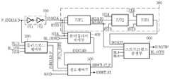
도 1은 본 발명의 실시예에 따른 데이터 스트로브 제어 장치의 구성도.
도 2는 도 1의 플러스 모드 제어부에 관한 상세 회로도.
도 3은 도 1의 저장부에 관한 상세 회로도.
도 4는 도 1의 온더플라이 제어부에 관한 상세 회로도.
도 5는 도 1의 경로 제어부에 관한 상세 회로도.
도 6은 도 1의 스트로브 펄스 발생부에 관한 상세 회로도.
도 7은 도 6의 스트로브 제어신호가 입력되는 장치의 주변 구성도.1 is a configuration diagram of a data strobe control apparatus according to an embodiment of the present invention;
2 is a detailed circuit diagram of the positive mode control unit of FIG.
3 is a detailed circuit diagram of the storage unit of FIG.
4 is a detailed circuit diagram of the on-the-fly control unit of FIG.
5 is a detailed circuit diagram of the path control unit of FIG.
6 is a detailed circuit diagram of the strobe pulse generator of FIG.
Fig. 7 is a peripheral configuration diagram of a device to which the strobe control signal of Fig. 6 is input. Fig.
이하, 첨부한 도면을 참조하여 본 발명의 실시예에 대해 상세히 설명하고자 한다.Hereinafter, embodiments of the present invention will be described in detail with reference to the accompanying drawings.
도 1은 본 발명의 일 실시예에 따른 데이터 스트로브 제어 장치의 구성도이다.1 is a configuration diagram of a data strobe control apparatus according to an embodiment of the present invention.
본 발명의 일 실시예에 따른 데이터 스트로브 제어 장치는 지연부(100), 플러스 모드 제어부(200), 저장부(300), 온더플라이 제어부(400), 경로 제어부(500) 및 스트로브 펄스 발생부(600)를 포함한다.A data strobe control apparatus according to an embodiment of the present invention includes a
먼저, 지연부(100)는 프리 클록 P_ENDCLK을 일정시간 지연하여 동작신호 ENDCLK을 출력한다. 이러한 지연부(100)는 프리 클록 P_ENDCLK을 비반전 구동하는 복수의 인버터 IV1, IV2를 포함한다. 본 발명의 실시예에서 지연부(100)의 인버터 IV1, IV2 개수를 2개로 설명하였지만, 본 발명은 이에 한정되는 것이 아니라 인버터의 개수를 다르게 설계할 수도 있다.First, the
플러스 모드 제어부(200)는 프리 클록 P_ENDCLK, 플러스 모드 신호 PLUS, 온더플라이 신호 BL_OTF 및 내부 클록 ICLK에 따라 플러스 온 더 플라이 모드인 경우에만 라이트 명령에 해당하는 프리 클록 P_ENDCLK를 입력받아 제어신호 ENDCLKD_P와 플러스 온더플라이 신호 PLUS_OTFB를 출력한다.The positive
저장부(300)는 동작신호 ENDCLK을 내부클록 ICLK에 동기시켜 저장한다. 이러한 저장부(300)는 복수의 플립플롭 F/F1~F/F3을 포함한다. 복수의 플립플롭 F/F1~F/F3은 리셋신호 RSTB에 따라 그 동작이 리셋된다.The
여기서, 플립플롭 F/F1은 동작신호 ENDCLK를 내부클록 ICLK에 동기시켜 저장하고 제어클록 DCLK05, DCLK10을 출력한다. 그리고, 플립플롭 F/F2은 제어클록 DCLK10을 내부클록 ICLK에 동기시켜 저장한다. 또한, 플립플롭 F/F3은 플립플롭 F/F2의 출력 클록을 내부클록 ICLK에 동기시켜 저장하고 제어클록 DCLK25을 출력한다.Here, the flip-flop F / F1 stores the operation signal ENDCLK in synchronization with the internal clock ICLK and outputs the control clocks DCLK05 and DCLK10. The flip-flop F / F2 stores the control clock DCLK10 in synchronization with the internal clock ICLK. The flip-flop F / F3 stores the output clock of the flip-flop F / F2 in synchronization with the internal clock ICLK and outputs the control clock DCLK25.
온더플라이 제어부(400)는 온더플라이 신호 BL_OTFB, 내부클록 ICLK 및 동작신호 ENDCLK에 따라 온더플라이 동작을 제어하여 제어신호 ENDCLKD을 출력한다. 온더플라이 신호 BL_OTFB는 온더플라이 신호 BL_OTF의 반전 신호이다.The on-the-
경로 제어부(500)는 제어신호 ENDCLKD, 플러스 온더플라이 신호 PLUS_OTFB, 제어신호 ENDCLKD_P 및 어드레스 ADD에 따라 노말 온 더 플라이 경로 또는 플러스 온 더 플라이 경로를 선택하기 위한 어드레스 래치신호 ADDWTLAT 또는 어드레스 래치신호 ADDWTLAT_P를 출력한다.The
스트로브 펄스 발생부(600)는 제어클록 DCLK25, 제어클록 DCLK05, 어드레스 래치신호 ADDWTLAT_P, 버스트 랭스 신호 BL4 및 버스트 랭스 신호 BL8에 따라 스트로브 펄스를 제어하여 온더플라이 신호 BL_OTFB 및 스트로브 제어신호 DINSTBP를 출력한다.The
본 발명의 실시예에서는 데이터 라이트 동작을 위해 미리 결정된 제 1버스트 길이의 데이터와 제 1버스트 길이의 데이터의 절반인 제 2버스트 길이의 데이터를 입력받는 것을 그 일 예로 설명한다. 여기서, 제 1버스트 길이의 데이터는 버스트 랭스 신호 BL8에 의해 입력되는 데이터를 의미하며, 제 2버스트 길이의 데이터는 버스트 랭스 신호 BL4에 의해 입력되는 데이터를 의미한다.In the embodiment of the present invention, data of a first burst length determined in advance for a data write operation and data of a second burst length, which is a half of data of the first burst length, are inputted. Here, the data of the first burst length means data input by the burst length signal BL8, and the data of the second burst length means data input by the burst length signal BL4.
도 2는 도 1의 플러스 모드 제어부(200)에 관한 상세 회로도이다.2 is a detailed circuit diagram of the positive
플러스 모드 제어부(200)는 복수의 낸드게이트 ND1~ND3와 복수의 인버터 IV3~IV5를 포함한다.The positive
여기서, 낸드게이트 ND1는 온더플라이 신호 BL_OTF와 플러스 모드 신호 PLUS를 낸드연산하여 플러스 온더플라이 신호 PLUS_OTFB를 출력한다. 그리고, 낸드게이트 ND2는 프리 클록 P_ENDCLK과 인버터 IV3에 의해 반전된 플러스 온더플라이 신호 PLUS_OTFB를 낸드연산한다. 또한, 낸드게이트 ND3는 내부클록 ICLK과 인버터 IV4에 의해 반전된 낸드게이트 ND2의 출력신호를 낸드연산한다. 인버터 IV5는 낸드게이트 ND3의 출력을 반전하여 제어신호 ENDCLKD_P를 출력한다.Here, the NAND gate ND1 performs the NAND operation of the on-the-fly signal BL_OTF and the positive mode signal PLUS to output the positive on-fly signal PLUS_OTFB. Then, the NAND gate ND2 performs a NAND operation on the positive clock pulse PLUS_OTFB inverted by the pre-clock P_ENDCLK and the inverter IV3. The NAND gate ND3 performs NAND operation on the output signal of the NAND gate ND2 inverted by the internal clock ICLK and the inverter IV4. The inverter IV5 inverts the output of the NAND gate ND3 and outputs the control signal ENDCLKD_P.
도 3은 도 1의 저장부(300)에 관한 상세 회로도이다.3 is a detailed circuit diagram of the
저장부(300)는 복수의 전송게이트 T1, T2와, 낸드게이트 ND4, 복수의 인버터 IV6~IV9 및 PMOS 트랜지스터 P1를 포함한다.The
여기서, 전송게이트 T1는 내부클록 ICLK와 인버터 IV6에 의해 반전된 내부클록 ICLK에 따라 동작신호 ENDCLK을 선택적으로 출력한다. 이러한 전송게이트 T1는 PMOS 게이트를 통해 내부클록 ICLK가 인가되고, NMOS 게이트를 통해 인버터 IV6에 의해 반전된 내부클록 ICLK가 인가된다.Here, the transfer gate T1 selectively outputs the operation signal ENDCLK according to the internal clock ICLK and the internal clock ICLK inverted by the inverter IV6. This transfer gate T1 is supplied with the internal clock ICLK through the PMOS gate and the internal clock ICLK inverted by the inverter IV6 through the NMOS gate.
그리고, 낸드게이트 ND4는 리셋신호 RSTB와 전송게이트 T1의 출력을 낸드연산하여 제어클록 DCLK05을 출력한다. 인버터 IV7는 3 상태 인버터에 해당하며 인버터 IV6의 출력에 따라 제어클록 DCLK05을 선택적으로 래치한다.The NAND gate ND4 performs a NAND operation on the reset signal RSTB and the output of the transfer gate T1 to output the control clock DCLK05. Inverter IV7 corresponds to a tri-state inverter and selectively latches control clock DCLK05 according to the output of inverter IV6.
또한, 전송게이트 T2는 내부클록 ICLK와 인버터 IV6에 의해 반전된 내부클록 ICLK에 따라 제어클록 DCLK05을 선택적으로 출력한다. 이러한 전송게이트 T2는 NMOS 게이트를 통해 내부클록 ICLK이 인가되고, PMOS 게이트를 통해 인버터 IV6에 의해 반전된 내부클록 ICLK 인가된다.In addition, the transfer gate T2 selectively outputs the control clock DCLK05 in accordance with the internal clock ICLK and the internal clock ICLK inverted by the inverter IV6. This transfer gate T2 is supplied with the internal clock ICLK through the NMOS gate and the internal clock ICLK inverted by the inverter IV6 through the PMOS gate.
그리고, 인버터 IV8, IV9는 전송게이트 T2의 출력을 래치하여 제어클록 DCLK10을 선택적으로 출력한다. 여기서, 인버터 IV9는 3 상태 인버터에 해당하며 내부클록 ICLK에 따라 전송게이트 T2의 출력을 선택적으로 래치한다.The inverters IV8 and IV9 latch the output of the transfer gate T2 and selectively output the control clock DCLK10. Here, the inverter IV9 corresponds to a tri-state inverter and selectively latches the output of the transmission gate T2 according to the internal clock ICLK.
도 4는 도 1의 온더플라이 제어부(400)에 관한 상세 회로도이다.4 is a detailed circuit diagram of the on-the-
온더플라이 제어부(400)는 복수의 낸드게이트 ND5, ND6 및 복수의 인버터 IV10~IV12를 포함한다.The on-die
여기서, 낸드게이트 ND5는 동작신호 ENDCLK, 내부클록 ICLK을 낸드연산한다. 그리고, 낸드게이트 ND6는 인버터 IV10에 의해 반전된 낸드게이트 ND5의 출력과 인버터 IV11에 의해 반전된 온더플라이 신호 BL_OTFB를 낸드연산한다. 또한, 인버터 IV12는 낸드게이트 ND6의 출력을 반전 구동하여 제어신호 ENDCLKD를 출력한다.Here, the NAND gate ND5 performs the NAND operation of the operation signal ENDCLK and the internal clock ICLK. The NAND gate ND6 performs the NAND operation on the output of the NAND gate ND5 inverted by the inverter IV10 and the on-the-fly signal BL_OTFB inverted by the inverter IV11. The inverter IV12 inverts the output of the NAND gate ND6 and outputs the control signal ENDCLKD.
도 5는 도 1의 경로 제어부(500)에 관한 상세 회로도이다.5 is a detailed circuit diagram of the
경로 제어부(500)는 어드레스 지연부(510), 선택부(520), 래치 L1, L2 및 초기화부(540)를 포함한다. 여기서, 어드레스 지연부(510)는 복수의 인버터 IV13~IV16을 포함하고, 선택부(520)는 전송게이트 T3, T4와, 인버터 IV17, IV18를 포함한다. 그리고, 래치 L1는 래치 구조의 인버터 IV19, IV20를 포함하고, 래치 L2는 래치 구조의 인버터 IV21, IV22를 포함한다. 또한, 초기화부(540)는 NMOS 트랜지스터 N1를 포함한다.The path control
복수의 인버터 IV13~IV15는 어드레스 ADD를 반전 지연한다. 그리고, 인버터 IV16는 인버터 VI14의 출력을 반전 지연한다.The plurality of inverters IV13 to IV15 reverse the address ADD. The inverter IV16 inverts and delays the output of the inverter VI14.
전송게이트 T3는 인버터 IV17에 의해 반전된 제어신호 ENDCLKD와 제어신호 ENDCLKD에 따라 인버터 IV15의 출력을 선택적으로 출력한다. 여기서, 전송게이트 T3는 PMOS 게이트를 통해 인버터 IV17에 의해 반전된 제어신호 ENDCLKD가 인가되고, NMOS 게이트를 통해 제어신호 ENDCLKD가 인가된다.The transfer gate T3 selectively outputs the output of the inverter IV15 according to the control signal ENDCLKD inverted by the inverter IV17 and the control signal ENDCLKD. Here, the control signal ENDCLKD inverted by the inverter IV17 is applied to the transfer gate T3 through the PMOS gate, and the control signal ENDCLKD is applied through the NMOS gate.
그리고, 전송게이트 T4는 인버터 IV18에 의해 반전된 제어신호 ENDCLKD_P와 제어신호 ENDCLKD_P에 따라 인버터 IV16의 출력을 선택적으로 출력한다. 여기서, 전송게이트 T4는 PMOS 게이트를 통해 인버터 IV18에 의해 반전된 제어신호 ENDCLKD_P가 인가되고, NMOS 게이트를 통해 제어신호 ENDCLKD_P가 인가된다.The transfer gate T4 selectively outputs the output of the inverter IV16 according to the control signal ENDCLKD_P inverted by the inverter IV18 and the control signal ENDCLKD_P. Here, the control signal ENDCLKD_P inverted by the inverter IV18 is applied to the transfer gate T4 through the PMOS gate, and the control signal ENDCLKD_P is applied through the NMOS gate.
래치 L1는 출력단과 입력단이 서로 연결된 인버터 IV19, IV20을 포함한다. 이러한 래치 L1는 전송게이트 T3의 출력을 일정시간 래치하여 어드레스 래치신호 ADDWTLAT를 출력한다.The latch L1 includes inverters IV19 and IV20 whose output and input are connected to each other. The latch L1 latches the output of the transfer gate T3 for a predetermined time and outputs the address latch signal ADDWTLAT.
여기서, 어드레스 래치신호 ADDWTLAT는 제어신호 ENDCLKD의 상태에 따라 버스트 랭스 신호 BL4 또는 버스트 랭스 신호 BL8 중 어느 하나를 선택하는 어드레스 ADD 제어신호이다.The address latch signal ADDWTLAT is an address ADD control signal for selecting either the burst length signal BL4 or the burst length signal BL8 according to the state of the control signal ENDCLKD.
그리고, 래치 L2는 출력단과 입력단이 서로 연결된 인버터 IV21, IV22을 포함한다. 이러한 래치 L2는 전송게이트 T4의 출력을 일정시간 래치하여 어드레스 래치신호 ADDWTLAT_P를 출력한다.The latch L2 includes inverters IV21 and IV22 whose output and input are connected to each other. The latch L2 latches the output of the transfer gate T4 for a predetermined time and outputs the address latch signal ADDWTLAT_P.
NMOS 트랜지스터 N1는 전송게이트 T4의 출력단과 접지전압단 사이에 연결된다. NMOS 트랜지스터 N1는 게이트 단자를 통해 플러스 온더플라이 신호 PLUS_OTFB가 인가된다.The NMOS transistor N1 is connected between the output terminal of the transfer gate T4 and the ground voltage terminal. The NMOS transistor N1 is supplied with the positive on-fly signal PLUS_OTFB through the gate terminal.
본 발명의 실시예에서는 초기화부(540)를 NMOS 트랜지스터 타입으로 설명하였지만, 본 발명의 실시예는 이에 한정되는 것이 아니며 PMOS 트랜지스터 타입으로 구현하여 플러스 온더플라이 신호 PLUS_OTFB의 반대 위상으로 제어할 수도 있다.In the embodiment of the present invention, the
도 6은 도 1의 스트로브 펄스 발생부(600)에 관한 상세 회로도이다.6 is a detailed circuit diagram of the
스트로브 펄스 발생부(600)는 노아게이트 NOR1, 복수의 낸드게이트 ND7~ND10 및 복수의 인버터 IV23~25를 포함한다.The
여기서, 노아게이트 NOR1는 버스트 랭스 신호 BL4와 버스트 랭스 신호 BL8를 노아연산한다. 그리고, 인버터 IV23는 노아게이트 NOR1의 출력을 반전 구동하여 온더플라이 신호 BL_OTFB를 출력한다.Here, the NOR gate NOR1 performs the NOR operation on the burst length signal BL4 and the burst length signal BL8. The inverter IV23 inverts the output of the NOR gate NOR1 to output an on-fly signal BL_OTFB.
그리고, 낸드게이트 ND7는 어드레스 래치신호 ADDWTLAT_P와 인버터 IV24에 의해 반전된 버스트 랭스 신호 BL4를 낸드연산하여 지연신호 DELAY_AD를 출력한다. 또한, 낸드게이트 ND8는 제어클록 DCLK05과 지연신호 DELAY_AD를 낸드연산한다. 그리고, 낸드게이트 ND9는 제어클록 DCLK25과 인버터 IV25에 의해 반전된 지연신호 DELAY_AD를 낸드연산한다. 낸드게이트 ND10는 낸드게이트 ND8, ND9를 낸드연산하여 스트로브 제어신호 DINSTBP를 출력한다.The NAND gate ND7 performs NAND operation on the address latch signal ADDWTLAT_P and the burst length signal BL4 inverted by the inverter IV24, and outputs the delay signal DELAY_AD. The NAND gate ND8 performs a NAND operation on the control clock DCLK05 and the delay signal DELAY_AD. The NAND gate ND9 performs a NAND operation on the delay signal DELAY_AD inverted by the control clock DCLK25 and the inverter IV25. The NAND gate ND10 performs NAND operation on the NAND gates ND8 and ND9 and outputs the strobe control signal DINSTBP.
이러한 구성을 갖는 본 발명의 실시예에 따른 데이터 스트로브 제어 장치의 동작 과정을 설명하면 다음과 같다.The operation of the data strobe control apparatus according to the embodiment of the present invention having such a configuration will be described below.
먼저, 지연부(100)는 프리 클록 P_ENDCLK을 일정시간 비반전 지연하여 동작신호 ENDCLK를 출력한다. 그리고, 플립플롭 F/F1은 이 동작신호 ENDCLK를 내부클록 ICLK에 동기시켜 제어클록 DCLK05을 스트로브 펄스 발생부(600)에 출력한다. 그리고, 플립플롭 F/F2은 플립플롭 F/F1으로부터 인가되는 제어클록 DCLK10을 내부클록 ICLK에 동기시켜 출력한다. 또한, 플립플롭 F/F3은 플립플롭 F/F2으로부터 인가되는 신호를 내부클록 ICLK에 동기시켜 제어클록 DCLK25을 스트로브 펄스 발생부(600)에 출력한다.First, the
여기서, 동작신호 ENDCLK는 라이트 동작 명령 신호에 해당할 수 있다. 하지만, 본 발명의 실시예는 이에 한정되는 것이 아니며 리드 동작 명령 신호에 따라 동작할 수도 있다. 이에 따라, 저장부(300)는 각각의 클록별로 지연된 라이트 동작 명령 신호를 생성하여 스트로브 펄스 발생부(600)에 출력한다. 즉, 저장부(300)는 버스트 랭스 별로 데이터 크기에 맞는 제어클록 DCLK05, DCLK25을 생성한다.Here, the operation signal ENDCLK may correspond to the write operation command signal. However, the embodiment of the present invention is not limited thereto and may operate according to the read operation command signal. Accordingly, the
또한, 온더플라이 제어부(400)는 동작신호 ENDCLK를 내부클록 ICLK에 동기시킨다. 그리고, 온더플라이 제어부(400)는 온 더 플라이 모드시 로우 레벨로 활성화되는 온더플라이 신호 BL_OTFB에 따라 제어신호 ENDCLKD를 출력한다. 즉, 온 더 플라이 모드시 온더플라이 신호 BL_OTFB가 로우 레벨이 되고 동작신호 ENDCLK가 하이 레벨이 되면 제어신호 ENDCLKD가 하이 레벨로 활성화 상태가 된다.Further, the on-die
경로 제어부(500)는 제어신호 ENDCLKD가 하이 레벨 상태로 활성화되면 어드레스 ADD를 입력받아 노말 온 더 플라이 경로를 선택하여 어드레스 래치신호 ADDWTLAT를 출력한다.When the control signal ENDCLKD is activated to the high level state, the
한편, 플러스 모드 제어부(200)는 플러스 모드 신호 PLUS와 온더플라이 신호 BL_OTF가 모두 활성화 상태가 되는 경우 플러스 온 더 플라이 모드로 판단하여 플러스 온더플라이 신호 PLUS_OTFB를 로우 레벨로 출력한다. 그리고, 플러스 모드 제어부(200)는 플러스 온더플라이 신호 PLUS_OTFB의 반전신호를 프리 클록 P_ENDCLK에 동기시켜 출력하고, 내부클록 ICLK의 활성화시 제어신호 ENDCLKD_P를 하이 레벨로 활성화시켜 출력한다. 즉, 플러스 온 더 플라이 모드인 경우에만 라이트 명령을 나타내는 프리 클록 P_ENDCLK를 입력받아 내부클록 ICLK에 동기된 제어신호 ENDCLKD_P를 출력한다.On the other hand, when both the plus mode signal PLUS and the on-the-fly signal BL_OTF are activated, the positive
이후에, 경로 제어부(500)는 플러스 온 더 플라이 모드에서 플러스 온더플라이 신호 PLUS_OTFB가 로우 레벨인 상태에서는 NMOS 트랜지스터 N1가 턴 오프 상태가 된다. 또한, 제어신호 ENDCLKD_P가 하이 레벨인 상태에서는 전송게이트 T4가 턴 온 되어 래치된 어드레스 래치신호 ADDWTLAT_P를 출력한다.Thereafter, when the positive on-fly signal PLUS_OTFB is at the low level in the positive on-fly mode, the
반면에, 경로 제어부(500)는 노말 온 더 플라이 모드시 제어신호 ENDCLKD가 하이 레벨인 상태에서는 전송게이트 T3 가 턴 온 되어 래치된 어드레스 래치신호 ADDWTLAT를 출력한다.On the other hand, when the control signal ENDCLKD is at the high level in the normal-on-the-fly mode, the
만약, 플러스 모드 신호 PLUS와 온더플라이 신호 BL_OTF 중 적어도 어느 하나의 신호가 로우 레벨로 인가되는 경우 플러스 온더플라이 신호 PLUS_OTFB가 하이 레벨 상태가 된다. 그러면, NMOS 트랜지스터 N1가 턴 온 되어, 래치 L2의 입력신호가 로우 레벨로 풀다운 구동된다. 이에 따라, 어드레스 래치신호 ADDWTLAT_P는 래치된 상태를 유지하게 된다.If at least one of the positive mode signal PLUS and the on-the-fly signal BL_OTF is applied at a low level, the positive on-fly signal PLUS_OTFB becomes a high level state. Then, the NMOS transistor N1 is turned on, and the input signal of the latch L2 is pulled down to the low level. As a result, the address latch signal ADDWTLAT_P maintains the latched state.
즉, 스트로브 펄스 발생부(600)는 노말 온 더 플라이 동작 모드시 버스트 랭스 신호 BL4, 버스트 랭스 신호 BL8 중 적어도 어느 하나의 신호가 하이 레벨로 활성화되는 경우 온더플라이 신호 BL_OTFB를 하이 레벨로 출력한다. 그러면, 온더플라이 제어부(400)는 노말 온 더 플라이 동작 모드로 판단하여 제어신호 ENDCLKD를 로우 레벨로 출력한다.That is, the
이에 따라, 경로 제어부(500)는 전송게이트 T3가 턴 오프 상태가 되고 어드레스 래치신호 ADDWTLAT가 래치 상태를 유지하게 된다. 그리고, 경로 제어부(500)는 NMOS 트랜지스터 N1가 턴 온 되어 어드레스 래치신호 ADDWTLAT_P가 하이 레벨로 래치된 상태를 유지한다.Accordingly, the
즉, NMOS 트랜지스터 N1가 풀다운 구동되는 경우 어드레스 래치신호 ADDWTLAT_P의 신호라인을 초기화시킨다. 초기 동작시 모드 레지스터 세트(MRS)에 의해 온 더 플라이 모드로 진입하기 이전까지 온 더 플라이 모드는 디폴트 상태인 로우 레벨이 되어 버스트 랭스 신호 BL8로 리셋된다.That is, when the NMOS transistor N1 is pulled down, the signal line of the address latch signal ADDWTLAT_P is initialized. The on-the-fly mode is set to the low level, which is the default state, and is reset to the burst length signal BL8 before the mode register set MRS enters the on-the-fly mode.
종래기술에서는 플러스 온 더 플라이 모드시 게이트의 단수 차이로 인해 버스트 랭스 신호 BL4, 버스트 랭스 신호 BL8를 결정하는 지연된 어드레스 래치신호 ADDTLAT와 제어클록 DCLK05 사이의 마진이 줄어들게 되었다. 특히, 반도체 메모리 장치가 저전압, 고 주파수화가 될수록 마진이 더욱 줄어든다.The margin between the delayed address latch signal ADDTLAT for determining the burst length signal BL4 and the burst length signal BL8 and the control clock DCLK05 is reduced due to the difference in the number of gates in the positive on-fly mode. In particular, as the semiconductor memory device is lowered in voltage and frequency, the margin is further reduced.
이에 따라, 본 발명의 실시예에서는 게이트 단수를 줄이고 경로 제어부(500)와 같이 노멀 온 더 플라이 모드와 플러스 온 더 플라이 모드의 경로를 분리하여 저전압, 고주파수 상태에서 발생할 수 있는 마진 포인트를 개선하도록 한다.Accordingly, in the embodiment of the present invention, the number of gates is reduced and the path of the normal-on-the-fly mode and the path of the positive on-fly mode is separated as in the
그리고, 스트로브 펄스 발생부(600)는 어드레스 래치신호 ADDWTLAT_P가 하이 레벨인 상태에서는 버스트 랭스 신호 BL4의 상태에 따라 지연신호 DELAY_AD의 레벨이 달라지게 된다. 즉, 버스트 랭스 신호 BL4가 로우 레벨이면, 제어클록 DCLK05이 하이 레벨인 상태에서 스트로브 제어신호 DINSTBP를 하이 레벨로 출력한다. 그리고, 버스트 랭스 신호 BL4가 하이 레벨이면, 제어클록 DCLK25이 하이 레벨인 상태에서 스트로브 제어신호 DINSTBP를 하이 레벨로 출력한다.When the address latch signal ADDWTLAT_P is at the high level, the
여기서, 스트로브 제어신호 DINSTBP는 내부클록 ICLK에 동기되어 버스트 랭스 신호 BL4에 해당하는 경우 2 클록에 해당하는 라이트 스트로브 펄스를 생성한다. 이에 따라, 버스트 랭스에 맞게 라이트 데이터를 셀에 액세스하게 된다. 만약, 스트로브 제어신호 DINSTBP가 버스트 랭스 신호 BL8에 해당하는 경우 4 클록에 해당하는 라이트 스트로브 펄스를 생성하여 라이트 데이터를 액세스한다.Here, the strobe control signal DINSTBP is synchronized with the internal clock ICLK to generate a write strobe pulse corresponding to two clocks when it corresponds to the burst length signal BL4. Thus, the write data is accessed to the cell in accordance with the burst length. If the strobe control signal DINSTBP corresponds to the burst length signal BL8, a write strobe pulse corresponding to four clocks is generated to access the write data.
즉, 플러스 온 더 플라이 모드시 프리 클록 P_ENDCLK과 내부클록 ICLK에 의해 동기된 어드레스 래치신호 ADDWTLAT_P가 생성된다. 그리고, 경로 제어부(500)는 이 어드레스 래치신호 ADDWTLAT_P에 의해 스트로브 제어신호 DINSTBP를 생성하게 된다. 스트로브 펄스 발생부(600)는 어드레스 래치신호 ADDWTLAT_P에 의해 어드레스 ADD를 빠르게 입력받아 제어클록 DCLK05와 지연신호 DELAY_AD와의 마진을 개선하여 저전압 또는 고속 모드에서 라이트 동작 속도를 향상시킬 수 있도록 한다.That is, in the positive on the fly mode, the pre-clock P_ENDCLK and the address latch signal ADDWTLAT_P synchronized by the internal clock ICLK are generated. The path control
도 7은 도 6의 스트로브 제어신호 DINSTBP가 입력되는 장치의 주변 구성도이다.FIG. 7 is a peripheral configuration diagram of a device to which the strobe control signal DINSTBP of FIG. 6 is input.
반도체 메모리 장치는 데이터를 처리하는 코어 영역과 외부의 다른 반도체 장치와 데이터를 주고 받는 입출력 영역으로 나눌 수 있다. 데이터 입출력 영역에는 외부에서 전달되는 데이터를 버퍼링하여 코어 영역으로 전달하기 위한 데이터 블록이 구비된다. The semiconductor memory device can be divided into a core region for processing data and an input / output region for exchanging data with another semiconductor device outside the semiconductor memory device. The data input / output area is provided with a data block for buffering data transmitted from the outside and transmitting the buffered data to the core area.
도 7의 실시예에서 데이터 입출력 영역은 데이터 입력부(700), 데이터 정렬부(710) 및 글로벌 입출력 전달부(720)를 포함한다. 데이터 입력부(700)는 라이트 동작을 라이트 데이터 DQ를 입력받는다. 여기서, 라이트 데이터 DQ는 미리 결정된 제 1 버스트 길이의 데이터이거나 제 1 버스트 길이의 절반인 제 2 버스트 길이의 데이터일 수 있다.7, the data input / output area includes a
예컨데, DDR3 SDRAM의 경우 모드 레지스터 세트(MRS)에서 라이트 동작의 버스트 길이(BL)를 설정할 때 BL4(Burst 4 mode), BL8(Burst 8 mode), OTF(On-the fly)의 세 가지인 경우로 나누어질 수 있다. BL8 동작인 경우 라이트를 위해 입력되는 데이터의 버스트 길이는 8 비트이다. 그리고, BL4 동작인 경우와 OTF 모드인 경우 라이트를 위해 입력되는 데이터의 버스트 길이는 4 비트이다.For example, in the case of DDR3 SDRAM, when setting the burst length (BL) of the write operation in the mode register set (MRS), three cases of BL4 (Burst 4 mode), BL8 (Burst 8 mode) and OTF . ≪ / RTI > In the case of the BL8 operation, the burst length of data input for writing is 8 bits. In the case of the BL4 operation and the OTF mode, the burst length of the data input for writing is 4 bits.
즉, OTF 모드로 설정된 경우 버스트 길이(BL)가 4 또는 8로 결정되지 않고, 리드 또는 라이트 명령이 입력된 당시의 어드레스 값이 0이냐 또는 1이냐에 의해 버스트 길이가 결정된다.That is, when the OTF mode is set, the burst length BL is not determined to be 4 or 8, and the burst length is determined by whether the address value at the time of inputting the read or write command is 0 or 1.
그리고, 데이터 정렬부(710)는 데이터 입력부(700)에 입력된 데이터를 정렬하여 제 1 버스트 길이의 데이터를 출력한다. 예컨데, DDR3 SDRAM인 경우 데이터 정렬부(710)는 데이터 입력부(700)로부터 라이징(Rising) 데이터 및 폴링(Falling) 데이터를 입력받아 스트로브 제어신호 DINSTBP의 폴링 에지 및 외부 클록신호의 라이징 에지에 정렬시켜 출력한다.The
본 발명의 실시예에 따른 데이터 스트로브 제어 장치는 스트로브 제어신호 DINSTBP가 글로벌 입출력 전달부(720)에 입력된다. 글로벌 입출력 전달부(720)는 데이터 정렬부(710)에 의해 정렬된 제 1 버스트 길이의 데이터를 입력받고, 제 1 버스트 길이의 데이터 또는 제 2 버스트 길이의 데이터를 글로벌 버스 GIO에 선택적으로 로딩한다. 즉, 스트로브 제어신호 DINSTBP의 활성화 시점에 동기하여 데이터를 글로벌 버스 GIO에 전달한다. 여기서, 글로벌 입출력 전달부(720)는 멀티플렉서, 입출력 센스앰프 등을 포함할 수 있다.The strobe control signal DINSTBP is input to the global input /
그리고, 글로벌 입출력 전달부(720)는 글로벌 버스 GIO를 통해 메모리 뱅크(730)에 연결된다. 메모리 뱅크(730)는 글로벌 버스상에 로딩된 해당 버스트 길이의 데이터를 셀에 라이트 한다.The global input /
Claims (13)
Translated fromKorean상기 온더플라이신호와 동작신호에 따라 제 2모드를 제어하기 위한 제 2제어신호를 출력하는 온더플라이 제어부;
상기 제 2모드시 상기 제 2제어신호에 따라 어드레스를 래치하고, 상기 제 1모드시 상기 제 1제어신호에 따라 상기 어드레스를 래치하여 어드레스 래치신호를 출력하는 경로 제어부; 및
상기 어드레스 래치신호와 버스트 랭스 신호에 대응하여 제어클록에 동기된 스트로브 제어신호를 출력하는 스트로브 펄스 발생부를 포함하는 것을 특징으로 하는 데이터 스트로브 제어 장치.A positive mode control unit for receiving a positive mode signal and an on-the-fly signal and outputting a first control signal and a positive on-fly signal for controlling the first mode;
An on-the-fly control unit for outputting a second control signal for controlling the second mode according to the on-the-fly signal and the operation signal;
A path control unit latching an address in accordance with the second control signal in the second mode, latching the address in accordance with the first control signal in the first mode, and outputting an address latch signal; And
And a strobe pulse generator for outputting a strobe control signal synchronized with a control clock corresponding to the address latch signal and the burst length signal.
라이트 명령을 나타내는 프리 클록, 상기 플러스 모드 신호, 상기 온더플라이 신호 및 상기 내부 클록의 조합에 따라 상기 제 1모드인 경우에만 상기 제 1제어신호와 상기 플러스 온더플라이 신호를 활성화시켜 출력하는 것을 특징으로 하는 데이터 스트로브 제어 장치.The apparatus of claim 1, wherein the positive mode control unit
And activates the first control signal and the positive on-fly signal only in the first mode in accordance with a combination of the pre-clock signal indicating the write command, the plus mode signal, the on-the-fly signal and the internal clock, And the data strobe control unit.
상기 온더플라이 신호, 내부클록 및 상기 동작신호에 따라 상기 제 2모드시 상기 제 2제어신호를 활성화시켜 출력하는 것을 특징으로 하는 데이터 스트로브 제어 장치.The apparatus according to claim 1, wherein the on-the-
And activates the second control signal in the second mode according to the on-the-fly signal, the internal clock, and the operation signal.
상기 어드레스를 일정시간 지연하는 어드레스 지연부;
상기 제 1제어신호와 상기 제 2어드레스의 활성화 상태에 따라 상기 어드레스를 선택적으로 출력하는 선택부;
상기 선택부의 출력을 래치하여 상기 어드레스 래치신호를 출력하는 래치를 포함하는 것을 특징으로 하는 데이터 스트로브 제어 장치.2. The apparatus of claim 1, wherein the path control unit
An address delay unit delaying the address by a predetermined time;
A selector for selectively outputting the address according to an activation state of the first control signal and the second address;
And a latch for latching an output of the selection unit and outputting the address latch signal.
상기 제 1제어신호의 활성화시 상기 어드레스를 출력하는 제 1선택부; 및
상기 제 2제어신호의 활성화시 상기 어드레스를 출력하는 제 2선택부를 포함하는 것을 특징으로 하는 데이터 스트로브 제어 장치.7. The apparatus of claim 6, wherein the selector
A first selector for outputting the address when the first control signal is activated; And
And a second selector for outputting the address when the second control signal is activated.
상기 제 1선택부의 출력을 래치하는 제 1래치; 및
상기 제 2선택부의 출력을 래치하는 제 2래치를 포함하는 것을 특징으로 하는 데이터 스트로브 제어 장치.8. The apparatus of claim 7, wherein the latch
A first latch for latching the output of the first selector; And
And a second latch for latching an output of the second selection unit.
상기 플러스 온더플라이 신호에 따라 상기 제 1선택부의 출력라인을 초기화시키는 초기화부를 포함하는 것을 특징으로 하는 데이터 스트로브 제어 장치.8. The apparatus of claim 7, wherein the path control unit
And an initialization unit for initializing an output line of the first selection unit according to the positive on-fly signal.
상기 어드레스 래치신호와, 제 1버스트 랭스 신호와, 제 2버스트 랭스 신호를 조합하여 제 1제어클록 또는 제 2제어클록에 동기된 상기 스트로브 제어신호를 출력하는 것을 특징으로 하는 데이터 스트로브 제어 장치.The apparatus of claim 1, wherein the strobe pulse generator
And outputs the strobe control signal synchronized with the first control clock or the second control clock by combining the address latch signal, the first burst length signal, and the second burst length signal.
Priority Applications (2)
| Application Number | Priority Date | Filing Date | Title |
|---|---|---|---|
| KR1020130068829AKR20140146331A (en) | 2013-06-17 | 2013-06-17 | Data strobe control device |
| US14/085,930US8929173B1 (en) | 2013-06-17 | 2013-11-21 | Data strobe control device |
Applications Claiming Priority (1)
| Application Number | Priority Date | Filing Date | Title |
|---|---|---|---|
| KR1020130068829AKR20140146331A (en) | 2013-06-17 | 2013-06-17 | Data strobe control device |
Publications (1)
| Publication Number | Publication Date |
|---|---|
| KR20140146331Atrue KR20140146331A (en) | 2014-12-26 |
Family
ID=52019114
Family Applications (1)
| Application Number | Title | Priority Date | Filing Date |
|---|---|---|---|
| KR1020130068829AWithdrawnKR20140146331A (en) | 2013-06-17 | 2013-06-17 | Data strobe control device |
Country Status (2)
| Country | Link |
|---|---|
| US (1) | US8929173B1 (en) |
| KR (1) | KR20140146331A (en) |
Families Citing this family (2)
| Publication number | Priority date | Publication date | Assignee | Title |
|---|---|---|---|---|
| KR102412609B1 (en)* | 2017-11-03 | 2022-06-23 | 삼성전자주식회사 | A memory device for storing and outputting an address accroding to an internal command and operating method thereof |
| US20220036238A1 (en)* | 2020-07-30 | 2022-02-03 | Tektronix, Inc. | Mono channel burst classification using machine learning |
Family Cites Families (4)
| Publication number | Priority date | Publication date | Assignee | Title |
|---|---|---|---|---|
| KR100257865B1 (en) | 1997-09-04 | 2000-06-01 | 윤종용 | Synchronous memory device with data input / output control circuit |
| US6850458B2 (en)* | 2002-11-14 | 2005-02-01 | Wen Li | Controlling data strobe output |
| JP4284527B2 (en) | 2004-03-26 | 2009-06-24 | 日本電気株式会社 | Memory interface control circuit |
| KR100805004B1 (en)* | 2006-06-15 | 2008-02-20 | 주식회사 하이닉스반도체 | A data strobe signal generator for generating a data strobe signal based on an adjustable preamble value and a semiconductor memory device including the same |
- 2013
- 2013-06-17KRKR1020130068829Apatent/KR20140146331A/ennot_activeWithdrawn
- 2013-11-21USUS14/085,930patent/US8929173B1/enactiveActive
Also Published As
| Publication number | Publication date |
|---|---|
| US20140369153A1 (en) | 2014-12-18 |
| US8929173B1 (en) | 2015-01-06 |
Similar Documents
| Publication | Publication Date | Title |
|---|---|---|
| US12019570B2 (en) | Apparatuses and methods including memory commands for semiconductor memories | |
| JP7229124B2 (en) | memory device | |
| US6259647B1 (en) | Synchronous semiconductor memory device allowing easy and fast test | |
| KR102164019B1 (en) | Burst Length control device and semiconductor device including the same | |
| US9281035B2 (en) | Semiconductor integrated circuit capable of controlling read command | |
| US7633833B2 (en) | Semiconductor memory device | |
| KR100719377B1 (en) | Semiconductor memory device that reads data patterns | |
| US8031553B2 (en) | Data strobe signal generating device and a semiconductor memory apparatus using the same | |
| US8050118B2 (en) | Semiconductor memory device | |
| KR20190112838A (en) | Apparatus and method for determining phase relationship between input clock signal and multiphase clock signal | |
| US11056171B1 (en) | Apparatuses and methods for wide clock frequency range command paths | |
| US9651983B2 (en) | Clock generation device and semiconductor device including the same | |
| US9368175B2 (en) | Semiconductor memory device receiving multiple commands simultaneously and memory system including the same | |
| US7706196B2 (en) | Semiconductor memory device | |
| KR20160035442A (en) | Semiconductor device | |
| US7995406B2 (en) | Data writing apparatus and method for semiconductor integrated circuit | |
| US10699768B2 (en) | Apparatuses and methods for command signal delay | |
| KR20140146331A (en) | Data strobe control device | |
| KR20200038833A (en) | Memory devices | |
| US8248863B2 (en) | Data buffer control circuit and semiconductor memory apparatus including the same | |
| KR100924017B1 (en) | Auto precharge circuit and auto precharge method | |
| KR20120087569A (en) | Test circuit | |
| JP2015032324A (en) | Semiconductor device |
Legal Events
| Date | Code | Title | Description |
|---|---|---|---|
| PA0109 | Patent application | Patent event code:PA01091R01D Comment text:Patent Application Patent event date:20130617 | |
| PG1501 | Laying open of application | ||
| PC1203 | Withdrawal of no request for examination | ||
| WITN | Application deemed withdrawn, e.g. because no request for examination was filed or no examination fee was paid |